OKI MSM7512B Technical data

E2A0014-16-X0
SUNSTAR电子元器件 http://www.sunstare.com/ TEL: 0755-83376282 FAX:0755-83376182 E-MAIL:szss20@163.com
SUNSTAR电子元器件 http://www.sunstare.com/ TEL: 0755-83778810 FAX:0755-83376182 E-MAIL:szss20@163.com
Semiconductor MSM7512B
¡ Semiconductor
This version: Jan. 1998
Previous version: Nov. 1996
MSM7512B
1200 bps Half Duplex FSK Modem – ITU-T V.23
GENERAL DESCRIPTION
The MSM7512B is useful for the ITU-T V.23 modem, for examples, low cost built-in modems,
telecontrol systems, home security systems, etc.
The family version, MSM7510 for ITU-T V.21, will be available following this device.
Oki has been mass-producing and delivering the MSM6926 and 6927 for a long time, but these
devices need two power supplies, +5 V for digital and +12 V for analog.
New generation devices, MSM7510/7512B, work with single rail +3 V to +5 V and low power
consumption.
FEATURES
• Conforms to ITU-T V.23, 1200 bps Half Duplex
• Conforms to ITU-T V.23, 75 bps transmitter
• Single Power Supply: +3 V to +5 V
• Low Power Consumption
Operating Mode: 25 mW Typ.
Power Down Mode: 0.1 mW Max.
• Line Hybrid Circuit on Chip
• Line Direct Drive Capability of Analog Output
• 3.579545 MHz Crystal Oscillator
• Digital Interface: TTL
• Package options:
16-pin plastic DIP (DIP16-P-300–2.54) (Product name: MSM7512BRS)
24-pin plastic SOP (SOP24-P-430-1.27–K) (Product name: MSM7512BGS-K)
1/12

SUNSTAR电子元器件 http://www.sunstare.com/ TEL: 0755-83376282 FAX:0755-83376182 E-MAIL:szss20@163.com
SUNSTAR电子元器件 http://www.sunstare.com/ TEL: 0755-83778810 FAX:0755-83376182 E-MAIL:szss20@163.com
Semiconductor MSM7512B
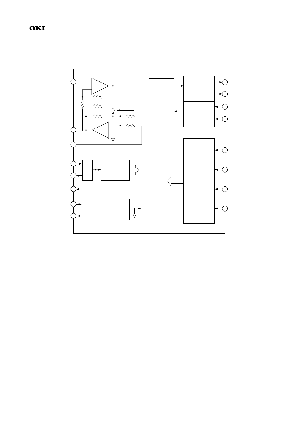
BLOCK DIAGRAM
AI
(2)
AO
(3)
EAI
(4)
X1
(6)
X2
(7)
CLK
(8)
V
DD
(1)
GND
(5)
*R1
OSC
+
–
*R1
*R2
*R2
–
+
CLK GEN.
SG GEN.
AOG
*R3
*R2
* R1 to R3 ≥ 50 kW
FSK & ANS
Bandpass
Filter
Demodulator
Modulator
CONT.
RD
(9)
CD
(10)
XD
(11)
RS
(12)
TEST
(13)
MOD1
(14)
MOD2
(15)
AOG
(16)
( ) : for MSM7512BRS
2/12

SUNSTAR电子元器件 http://www.sunstare.com/ TEL: 0755-83376282 FAX:0755-83376182 E-MAIL:szss20@163.com
SUNSTAR电子元器件 http://www.sunstare.com/ TEL: 0755-83778810 FAX:0755-83376182 E-MAIL:szss20@163.com
Semiconductor MSM7512B
PIN CONFIGURATION (TOP VIEW)
1
DD
2
AI
3
AO
4
EAI
5
GND
6
X1
7
X2
8 9
CLK
16-Pin Plastic DIP
16V
15
14
13
12
11
10
AOG
MOD2
MOD1
TEST
RS
XD
CD
RD
1
DD
2
NC
3
AI
4
NC
5
AO
6
EAI
7
GND
8
X1
9
NC
10
X2
11
NC
12 13
CLK
24-Pin Plastic SOP
NC : No connect pin
24V
23
22
21
20
19
18
17
16
15
14
AOG
NC
MOD2
NC
MOD1
TEST
RS
XD
NC
CD
NC
RD
3/12

SUNSTAR电子元器件 http://www.sunstare.com/ TEL: 0755-83376282 FAX:0755-83376182 E-MAIL:szss20@163.com
SUNSTAR电子元器件 http://www.sunstare.com/ TEL: 0755-83778810 FAX:0755-83376182 E-MAIL:szss20@163.com
Semiconductor MSM7512B
PIN DESCRIPTION
No.
RS GS-VK
11 VDD— +3 V to +5 V Power Supply
2 3 AI I Analog receive signal input.
3 5 AO O Analog transmit signal output.
External analog signal input.
4 6 EAI I
5 7 GND — Ground, 0 V.
6 8 X1 I
710 X2 O
8 12 CLK O 3.579545 MHz clock signal output.
913 RD O
10 15 CD O
11 17 XD I*
12 18 RS I*
13 19 TEST I*
14 20 MOD1 I* Operation mode select.
15 22 MOD2 I*
16 24 AOG I*
The signal applied to this pin is transmitted from AO via transmit output
amplifier. When not using this pin, it should be left open.
3.579545 MHz crystal resonator should be connected to X1 and X2.
When applying external clock 3.579545 MHz to the device, it should be
applied to X2 (not X1) via an AC-coupling capacitor of 100 pF and X1
has to be opened.
Modem receive serial data output.
Digital "1" and "0" correspond to "Mark" and "Space", respectively. When
CD (Carrier Detect) is off, RD is held at "Mark" state.
FSK Receive signal and answer tone detect.
Digital "0" and "1" represent "Detect" and "Non-detect", respectively.
Modem transmit serial data input.
Digital "1" and "0" correspond to "Mark" and "Space", respectively.
FSK signal and answer tone transmit enable.
When digital "0" is applied to RS, transmitting becomes enable.
Chip test input.
TEST should be open or digital "1".
Refer to Table 1.
Analog transmit signal amplitude select.
Digital "1" Æ –10 dBm Typ. at AO
Digital "0" Æ –4 dBm Typ. at AO
DescriptionName I/O
Note : I* : Internally pulled-up input pin.
4/12
 Loading...