

Datasheet MSM5412222A-25JS, MSM5412222A-25TS-K, MSM5412222A-30JS, MSM5412222A-30TS-K Datasheet (OKI)

The OKI MSM5412222A is a high performance 3-Mbit, 256K X 12-bit, Field Memory. It is
especially designed for high-speed serial access applications such as HDTVs, conventional
NTSC TVs, VTRs, digital movies and Multi-media systems. MSM5412222A is a FRAM for wide
or low end use in general commodity TVs and VTRs exclusively. MSM5412222A is not
designed for high end use in medical system s, professional graphics system s which require
long term picture stor ag e, da ta s t or age systems and others . T wo or more MSM5412222As can
be cascaded directly without any delay devices between them. (Cascading provides larger
storage depth or a longer delay).
Each of the 12-bit planes has separ ate seri al write and read ports. Thes e emplo y independ ent
control clocks to support asynchronous read and write operations. Different clock rates are also
supported, which allow alternate data rates between write and read data streams.
The MSM5412222A provides high speed FIFO, First-In First-Out, operation without external
refreshing: MSM541 2222A refreshes its DRAM s torage cells autom atically, so that it appears
fully static to the users.
Moreover, fully static t ype m emor y cells a nd dec oder s for s eria l acces s ena ble the ref resh f ree
serial access operation, so that s erial read a nd/or write contro l clock can be halted h igh or low
for any duration as long as t he power is on. Interna l conf licts of mem or y access and ref reshi ng
operations are prevented by special arbitration logic.
The MSM5412222A ’s function is s imple, and s imilar to a d igital delay device whos e delay-bitlength is easily set by reset timing. The delay length, and the number of read delay clocks
between write and read, is determined by externally controlled write and read reset timings.
Additional SRAM serial registers, or line buffers for the initial access of 256 X 12-bit enable high
speed first-bit-access with no clock delay just after the write or read reset timings.
Additionally, the MSM54122 22A has a write mask function or input enable function (IE) , and
read-data skipping function or output enable function (OE). The differences between write
enable (WE) and input enable (IE), and between read en able (RE) and out put ena ble ( OE) are
that WE and RE can stop serial wr ite/read addr ess incr em ents, but IE and OE cannot stop the
increment, when write/read clocking is continuously applied to MSM5412222A. The input
enable (IE) function a llows the user to wr ite into s elec ted loc atio ns of the mem or y only, leaving
the rest of the memory contents unchanged. This facilitates data processing to display a
“picture in picture” on a TV screen.
The MSM5412222A is similar in operation and functionality to OKI 1-Mbit Field Memor
y
MSM514222C and 2-Mbit Field Memory MSM518222A. Three MSM514222Cs or one
MSM514222C plus one MSM518222A can be replaced simply by one MSM5412222A.
OKI
Semiconductor
MSM5412222A
262,214-Word x 12-Bit Field Memory
DESCRIPTION
REVISION-3 1999.6.10
OKI Semiconductor MSM5412222A
2
Single power supply : 5 V ±10%
512 Rows X 512 Columns X 12 bits
Fast FIFO (First-In First-Out) operation
High speed asynchronous serial access
Read/write cycle time 25 ns/30 ns
Access time 23 ns/25 ns
Direct cascading capab il ity
Write mask function (Input enable control)
Data skipping function (Output enable control)
Self refresh (No refresh control is required)
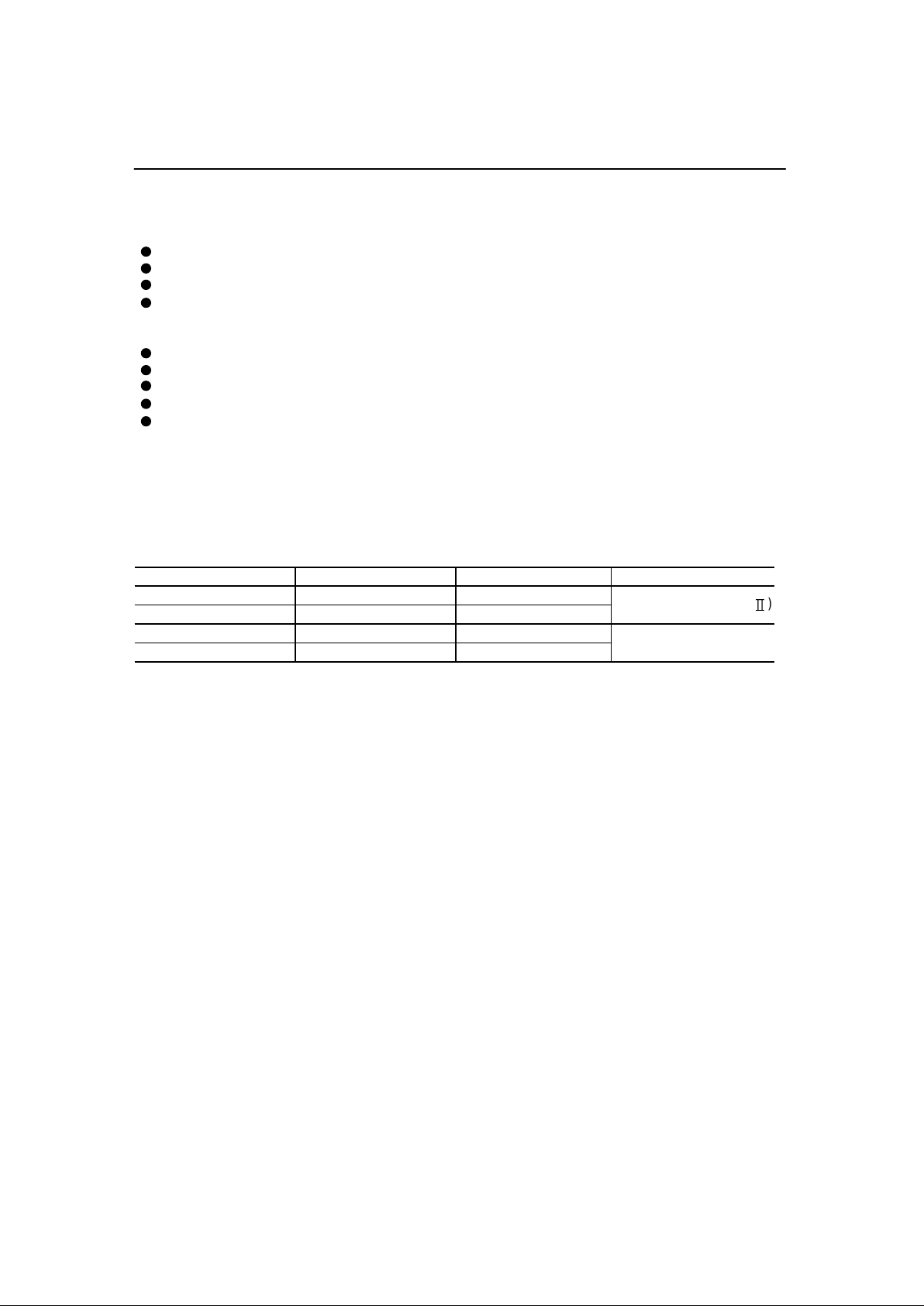
Package options:
44-pin 400 mil plastic TSOP (Type II) (TSOPII44-P-400-0.80-K) (Product : MSM5412222A-xxTS-K)
40-pin 400 mil plastic SOJ (SOJ40-P-400-1.27) (Product : MSM5412222A-xxJS)
xx indicates speed rank.
FEATURES
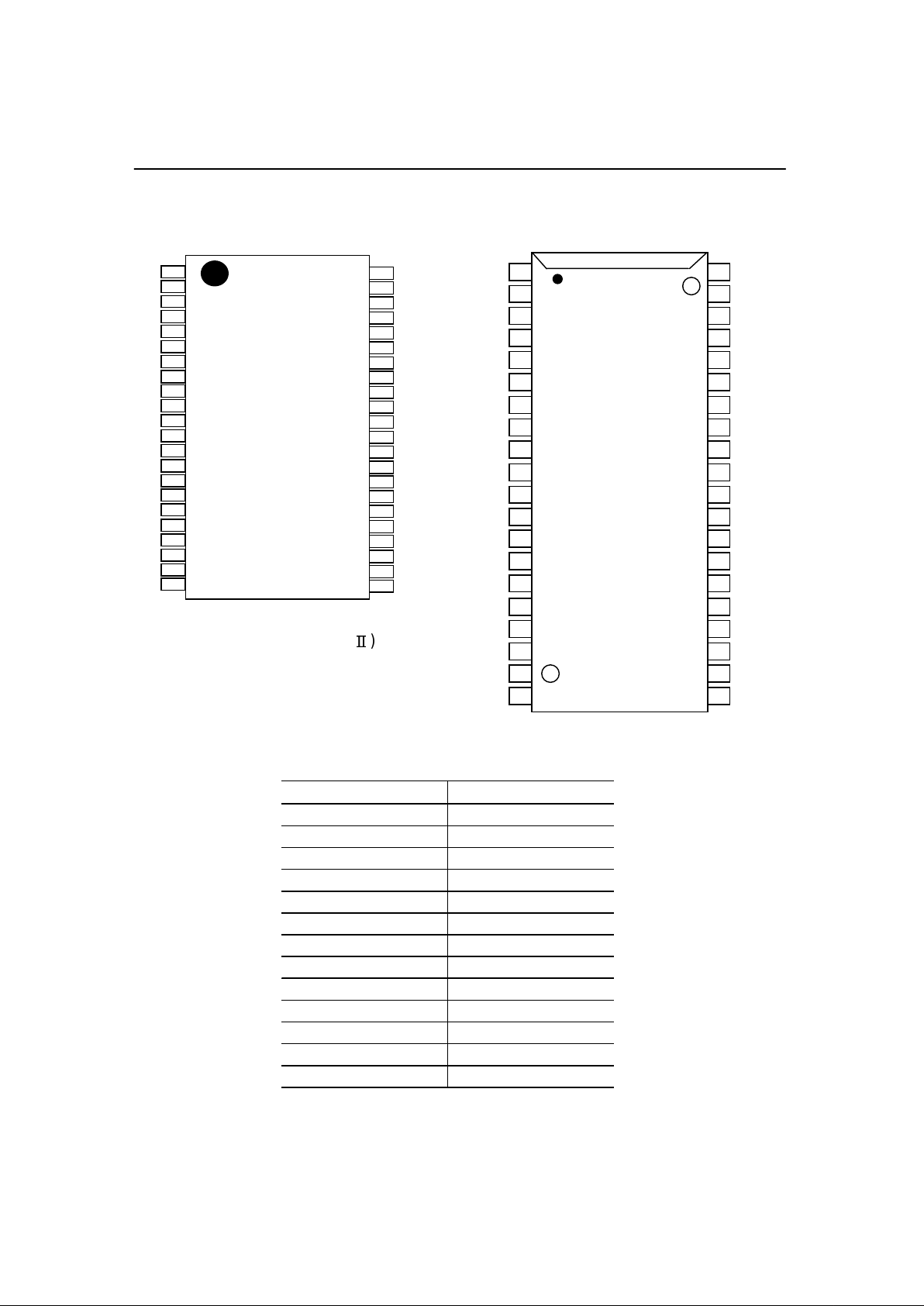
Package
400 mil 44-Pi n TSOP (þ)
400 mil 40-pin S OJ
Cycle Ti me(M in . )
25ns
30ns
25ns
30nsMS M5412222A -30JS
Acce ss Tim e(M ax.)
23ns
25ns
23ns
Family
MS M5412222A -25TS-K
MS M5412222A -30TS-K
MS M5412222A -25JS
25ns
PRODUCT FAMILY
OKI Semiconductor MSM5412222A
3
PIN CONFIGURATION(TOP VIEW)
Pin Name Function
SWCK
SRCK
Serial Write Clock
Serial Read Clock
Write EnableWE
RE Rea d Enabl e
IE In p ut Enable
OE Output Enable
RSTW Write Reset Clock
RSTR Rea d Reset Clo ck
D
IN
0-11
Data Input
D
OUT
0-11
Data Output
Vcc
Vss
NC
Power Suppl
y(5V)
Ground(0V
)
No Connection
1
2
3
4
5
6
7
8
9
10
11
12
13
14
15
16
17
18
19
20
40
39
38
37
36
35
33
34
32
31
30
29
28
27
26
25
24
23
22
21
Vss
NC
D
IN
11
D
IN
10
D
IN
9
D
IN
8
D
IN
7
D
IN
6
D
IN
5
D
IN
4
D
IN
3
D
IN
2
D
IN
1
D
IN
0
SWCK
RSTW
WE
IE
NC
Vcc
Vss
NC
D
OUT
11
D
OUT
10
D
OUT
9
D
OUT
8
D
OUT
7
D
OUT
6
D
OUT
5
D
OUT
4
D
OUT
3
D
OUT
2
D
OUT
1
D
OUT
0
SRCK
RSTR
RE
OE
Vss
Vcc
Vss
D
OUT
11
D
OUT
10
NC
D
OUT
9
D
OUT
8
D
OUT
7
D
OUT
6
NC
D
OUT
5
D
OUT
4
D
OUT
3
D
OUT
2
Vss
D
OUT
1
D
OUT
0
SRCK
RSTR
NC
RE
OE
Vcc
1
2
3
4
5
6
7
8
9
10
11
12
13
14
15
16
17
18
19
20
21
22
44
43
42
41
40
39
38
37
36
35
34
33
32
31
30
29
28
27
26
25
24
23
Vss
D
IN
11
D
IN
10
NC
D
IN
9
D
IN
8
D
IN
7
D
IN
6
NC
D
IN
5
D
IN
4
D
IN
3
D
IN
2
NC
D
IN
1
D
IN
0
SWCK
RSTW
NC
WE
IE
Vcc
40-PIN Pla stic SOJ
44-PIN Plastic TSOP()
(K Type)
NOTE:The same power supply voltage must be provided to every Vccpin, and the same GND
voltage level must be provided to every Vss pin.
OKI Semiconductor MSM5412222A
4
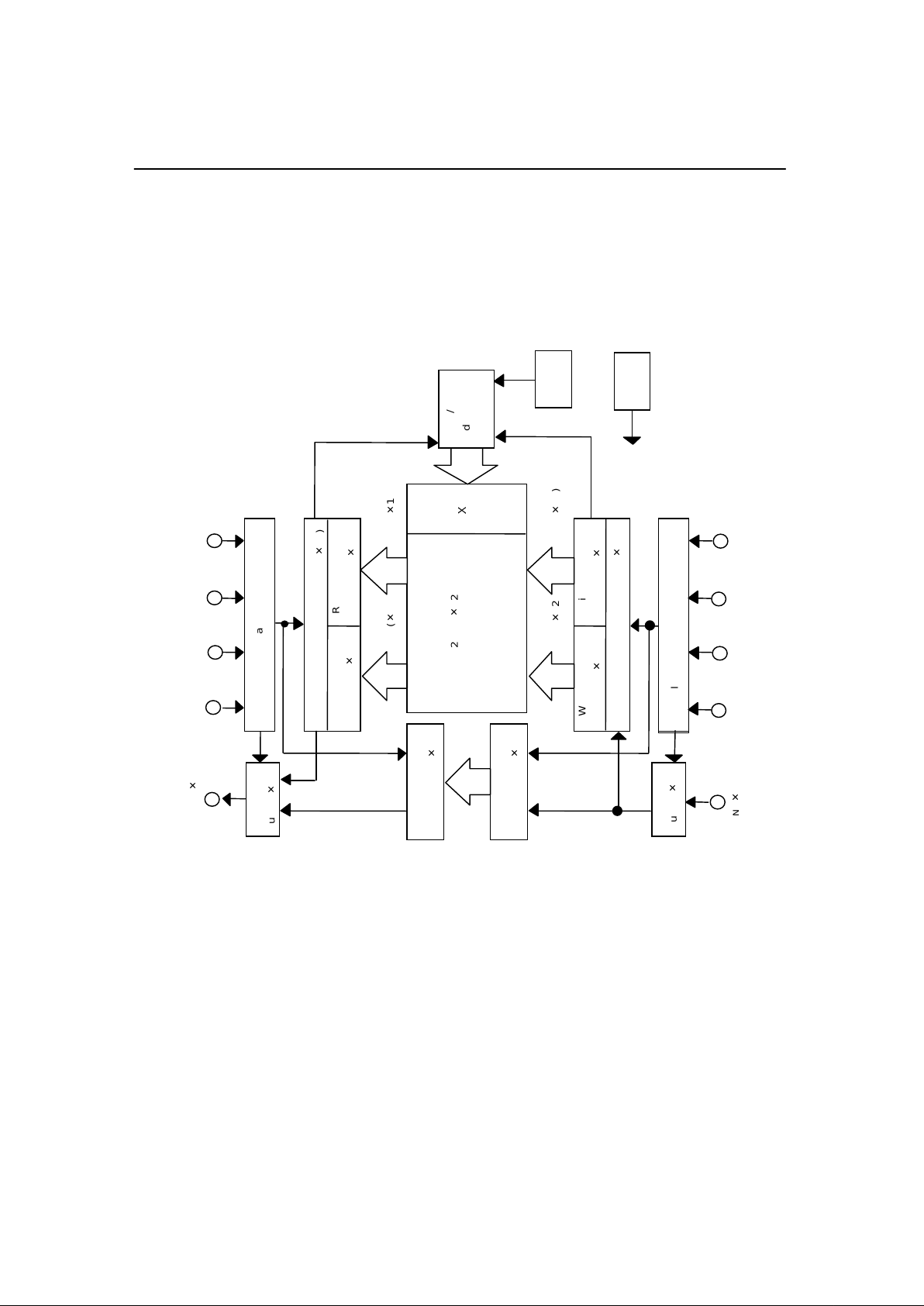
BLOCK DIAGRAM
Clock
Oscillator
VBB
Generator
-
256k (
q
12)
Memory
Array
512 Word Serial Read Register (
q
12)
Read Line Buffer
Low-Half (
q
12)
Read Line Buffer
High-Half (
q
12)
Write Line Buffer
Low-Half (
q
12)
Write Line Buffer
High-Half (
q
12)
512 Word Serial Write Register (
q
12)
256 (
q
12) 256 (
q
12)
256 (
q
12) 256 (
q
12)
Serial
Read
Controller
RE
RSTR
SRCK
WE RSTW
SWCK
71 Word
Sub-Register (
q
12)
Data-In
Buffer (
q
12)
Data-Out
Buffer (
q
12)
D
OUT
(
q
12)
D
IN
(
q
12)
Read/Write
and Refresh
Controller
IE
71 Word
Sub-Register (
q
12)
Decoder
OE
Serial
Write
Controller

OKI Semiconductor MSM5412222A
5
Write Operation
The write operation is co ntrolled by three clocks , SWC K, RSTW, and W E. Write operation is
accomplished by c ycling SWCK, and holding WE high after the write address point er reset
operation or RSTW.
Each write operation, which begins after RSTW, must contain at least 80 active write cycles,
i.e. SWCK cycles while WE is high. To transfer the last data to t he DRAM array, which at that
time is stored in the serial data registers attached to the DRAM arra y, an RSTW operation is
required after the last SWCK cy cle.
Note that every write timing of MSM5412222A is delayed by one clock compared with read
timings for easy c ascading without any interface delay devices.
Write Reset : RSTW
The first positive transition of SWCK after RSTW becomes high resets the write address
counters to zero. RSTW setup and hold times are referenced to the rising edge of SWCK.
Because the write reset function is solely controlled by the SWCK rising edge after the high
lev el of RSTW, the states of WE and IE are ignored in the write reset cycle.
Before RSTW may be brought high again for a further reset operation, it must be low for at
least two SWCK cycles.
Data Inputs : D
IN
0 - 11
Write Clock : SWCK
The SWCK latches the inp ut dat a on chi p when WE is high, and a lso increm ents the internal
write address pointer. Data-in setup time t
DS
, and hold time t
DH
are referenced to the rising
edge of SWCK.
Write Enable : WE
WE is used for data write enable/disable control. WE high level enables the input, and WE
low level disables the input and holds the internal write address pointer. There are no WE
disable time (low) and WE enable time (high) restrictions, because the MSM5412222A is in
fully static operation as long as the power is on. Note that WE setup and hold times are
referenced to t he rising edge of SWCK.
Input Enable : IE
IE is used to enab le/ disable writing into memory. IE high level en ables writing. The internal
write address pointer is always incremented by cycling SWCK regardless of the IE level.
Note that IE setup and hold ti mes are referenced to the rising edge of SWCK.
OPERATION

OKI Semiconductor MSM5412222A
6
Read Operation
The read operati on is contro lled by t hree clocks, SR CK, R STR, and RE. Read operation is
accomplished by cycling SRCK, and holding RE high after the read address pointer reset
operation or RSTR.
Each read operation, which begins after RSTR, must contain at least 80 active read cycles,
i.e. SRCK cycl es while RE is high.
Read Reset : RSTR
The first positive transition of SRCK after RSTR becomes high resets the read address
counters to zero. RSTR setup and hold times are referenced to the rising edge of SRCK.
Because the read reset function is solely controlled by the SRCK rising edge after the high
level of RSTR, the states of RE and OE are ignored in the read reset cycle.
Before RSTR may be brought high again for a further reset operation, it must be low for at
least *two SRCK cycles.
Data Out : D
OUT
0 - 11
Read Clock : SRCK
Data is shifted out of the data registers. It is triggered by the rising edge of SRCK when RE
is high during a read operation. The SRCK input increments the internal read address
pointer when RE is high.
The three-state output buffer provides direct TTL compatibility ( no pullup resistor required).
Data out is the same polarity as data in. The output becomes valid after the access time
interval t
AC
that begins with the rising edge of SRCK. *There are no output valid time
restriction on MSM5412222A.
Read Enable : RE
The function of RE is to gate of the SRCK clock for incrementing the read pointer. When RE
is high before t he rising edge of S RCK, the rea d pointer is i ncrement ed. When R E is l o w, the
read pointer is not incremented. RE setup times (t
RENS
and t
RDSS
) and RE hold times (t
RENH
and t
RDSH
) are referenced t o the rising edge of t he SRCK clock.
Output Enabl e : OE
OE is used to enable/disable the outputs. OE high level enables the outputs. The internal
read address pointer is always incremented by cycling SRCK regardless of the OE level.
Note that OE setup and hold t imes are referenced to the rising edge of SR CK.

OKI Semiconductor MSM5412222A
7
Power-up and Initialization
On power-up , t he de vic e is des igned to beg in proper oper ation af ter at least 100 us aft er V
CC
has stabilized to a value within the range of recommended operating conditions. After this
100 us stabilization interval, the following initialization sequence must be performed.
Because the read and write address counters are not valid after power-up, a minimum of 80
dummy write operations (SWCK cycles) and read operations (SRCK cycles) must be
performed, f ollowed by an RSTW o per at ion a nd an RST R oper ati on, to properly in itia liz e the
write and the read address pointer. Dummy write cycles/RSTW and dummy read
cycles/RSTR ma y occur simultaneously.
If these dummy read and write operations start while V
CC
and/or the substrate voltage has
not stabilized, it is necessary to perform an RSTR operation plus a minimum of 80 SRCK
cycles plus another RSTR operation, and an RSTW operation plus a minimum of 80 SRCK
cycles plus another RSTW op eration to properly initializ e read a nd write address pointers.
Old/New Data Access
There must be a minimum delay of 600 SWCK cycles between writing into memory and
reading out from memory. If reading from the first field starts with an RSTR operat ion, before
the start of writing the second field (before the next RSTW operation), then the data just
written will be read out.
The start of reading out the first field of data may be delayed past the beginning of writing in
the second field of data for as many as 70 SWCK cycles. If the RSTR operation for the first
field read-out occurs less than 70 SWCK cycles after the RSTW operation for the second
field write-in, then the inter nal buffering of the device assures that the first fiel d will still be
read out. The first field of data that is read out while the second field of data is written is
called “old data”.
In order to read out “new data”, i. e., the second field written in, the delay between an RSTW
operation and an RSTR operation must be at least 600 SRCK cycles. If the delay between
RSTW and RSTR operations is more than 71 but less than 600 cycles, then the data read
out will be undetermined. It may be “old d ata” or “ne w” data, or a combinat ion of o ld and new
data. Such a timing should be a voided.
Cascade Operation
The MSM5412222A is designed to allow easy cascading of multiple memory devices. This
provides higher storage depth, or a longer delay than can be achieved with only one
memory device.

OKI Semiconductor MSM5412222A
8
Symbol Unit
V
T
V
I
OS
mA
P
D
W
T
OPR
u
T
STG
u
Rating
50
Condition
at Ta=25u,Vss
Ta=25
u
-
-1.0 to 7.0
Operating Temperature
Storage Temperature
Ta=25
u
1
0 to 70
-55 to 150-
Parameter
Input Output Voltage
Output Current
Power Dissipation
Sym b ol Unit
Vcc V
Vss V
V
IH
V
V
IL
V
0
Max.
5.5
0
Vcc+1
0.8
Typ.
5.0
0
Vcc
Input Low Voltage
Min.
4.5
0
2.4
-1.0
Parameter
Power Supply Voltage
Power Supply Voltage
Input H igh Voltage
Symbol Min. Max. Unit
I
LI
-10 10 uA
I
LD
-10 10 uA
V
OH
2.4 - V
V
OL
-0.4V
I
CC1
-90mA
I
CC2
-5mA
Operating Current Minim um Cy c l e Time, Out put Open
St andby Current
In pu t Pin=VIH/V
IL
IOL=2mA
Condition
0<VI<Vcc+ 1,Other Pins Tested at V= 0V
0<Vo<Vcc
I
OH
=-1mA
Output "L" Level Volt age
Parameter
Input Leakage Current
Output Leakge Current
Output "H" Level Voltage
ELECTRICAL CHARACTERISTICS
Absolute Maximum Ratings
Recommended Operating Conditions
DC Characteristics
Capacitance
Symbol Max. Unit.
C
I
7pF
C
O
10 pF
Input Capac i t ance(DIN,SWCK,SRCK,RSTW,RSTR,WE,RE,IE,OE)
Output Capacitance(D
OUT
)
Parameter
(Ta=25
u
㺮ÊÅ÷¦

OKI Semiconductor MSM5412222A
9
Min. Max. Min. Max.
t
AC
- 23 - 25 ns
t
DDCK
6-6-ns
t
DECK
623625ns
t
WSWH
9-12-ns
t
WSWL
10 - 12 - ns
t
DS
2-2-ns
t
DH
4-4-ns
t
WENS
0-0-ns
t
WENH
3-3-ns
t
WDSS
0-0-ns
t
WDSH
3-3-ns
t
IENS
0-0-ns
tIENH
3-3-ns
t
IDSS
0-0-ns
t
IDSH
3-3-ns
t
WWEH
5-10-ns
t
WWEL
5-10-ns
t
WIEH
5-10-ns
t
WIEL
5-10-ns
t
RSTWS
0-0-ns
t
RSTWH
3-3-ns
t
WSRH
9-12-ns
t
WSRL
10 - 12 - ns
t
RENS
0-0-ns
t
RENH
3-3-ns
t
RDSS
0-0-ns
t
RDSH
3-3-ns
t
OENS
0-0-ns
t
OENH
3-3-ns
t
ODSS
0-0-ns
t
ODSH
3-3-ns
t
OEZ
917917ns
t
WREH
5-10-ns
t
WREL
5-10-ns
t
WOEH
5-10-ns
t
WOEL
5-10-ns
t
RSTRS
0-0-ns
t
RSTRH
3-3-ns
t
SWC
25 - 30 - ns
t
SRC
25 - 30 - ns
t
T
330330ns
RE Disable Hold Time
SRCK "L" Pulse Width
RE Enable Setup Time
RE Enable Hold Time
RE Disable Setup Time
IE "L" Pulse Width
RSTW Setup Time
RSTW Hold Time
SRCK "H" Pulse Width
I E Disable Hold Time
WE "H" Pulse Width
WE "L" Pulse Width
IE "H" Pulse Width
WE Disable Hold Time
IE Enable Setup Time
IE Enable Hold Time
IE Disable Setup Time
I nput Data Hold Time
WE Enable Setup Time
WE Enable Hold Time
WE Disable Setup Time
D
OUT
Enable Time from SRCK
SWCK "H " Pulse Width
SWCK "L" Pulse Width
Input Data Setup Time
Paramete r Symbol
Access T ime from SRCK
D
OUT
Hold Time from SRCK
RE "H" Pu l se Width
RE "L" Pul se Width
OE "H" Pulse Width
OE Enable Setup Time
OE Enable Hold Time
OE Disable Setup Time
OE Disable Hold Time
Unit
SRCK Cycle Time
Transition Time(Rise and Fall)
MSM5412222A-25 MSM5412222A-30
OE "L" Pulse Width
RSTR Setup Time
RSTR Hold Time
SWCK Cycle Time
Output Buffer Turn-off Delay Time fr om O E
AC Characteristics
(Vcc=5Vp10%, Ta=0u to 70u)

OKI Semiconductor MSM5412222A
10
1. I nput signal reference levels for the parameter measurement are V
IH
= 3.0 V and VIL= 0 V.
The transition time t
T
is defined to be a transition time that signal transf ers betw een V
IH
=
3.0 V and V
IL
= 0 V.
2. AC measurements assume t
T
= 3 ns.
3. Read address mus t have more than a 600 address delay than write address in ev ery cycle
when asynchronous read/write is performed.
4. Read must have more than a 600 address delay t han write in order to read the data
written in a current series of write cycles which has been started at last write reset cycle:
this is called "new data read".
When read has less than a 70 address delay than write, the read data are the data written
in a previous series of write cycles which had been written before at last write reset cycle:
this is called "old data read".
5. When the read ad dress delay is between more than 71 and less than 599, read data will
be undetermined. Howev er, normal write is achieved in this address condition.
6. Out puts are measured with a load equivalent to 1 TTL load and 30 pF. Output reference
levels are V
OH
= 2.0 V and V
OL
= 0.8 V.
Notes:

OKI Semiconductor MSM5412222A
11
TIMING WAVEFORM
Write Cycle Timing(Write Reset)
Write Cycle Timing(Write Enable)
DIN
n cycle
0 cycle 1 cycle 2 cycle
tDS
tDH
tRSTWS
tRSTWH
tWSWH
tWSWL
tSWC
n-1 n 0 1 2
SWCK
RSTW
WE
IE
V
IH
V
IL
V
IH
V
IL
V
IH
V
IL
V
IH
V
IL
V
IH
V
IL
tT
n cycle
Disable cycle n+1 cycle
tWENH
tWWEL
tWENS
Disable cycle
tWDSH
tWWEH
tWDSS
n-1 n
n+1
D
IN
SWCK
WE
IE
RSTW
V
IH
V
IL
V
IH
V
IL
V
IH
V
IL
V
IH
V
IL
V
IH
V
IL

OKI Semiconductor MSM5412222A
12
Read Cycle Timing(Read Reset)
Write Cycle Timing(Input Enable)
D
IN
WE
RSTW
tWIEH
n-1 n
n+3
V
IH
V
IL
V
IH
V
IL
V
IH
V
IL
V
IH
V
IL
V
IH
V
IL
n cycle
n+1 cycle n+3 cycle
tIENH
tIENS
n+2 cycle
tIDSH
tIDSS
SWCK
IE
tWIEL
D
OUT
RSTR
RE
OE
tAC
V
IH
V
IL
V
IH
V
IL
V
OH
V
OL
V
IH
V
IL
V
IH
V
IL
n-1 n 0 1 2
tDDCK
n cycle
0 cycle 1 cycle 2 cycle
tRSTRS
tRSTRH
tWSRH
tWSRL
tSRC
tT
SRCK

OKI Semiconductor MSM5412222A
13
Read Cycle Timing(Read Enable)
Read Cycle Timing(Output Enable)
SRCK
RE
D
OUT
OE
RSTR
V
IH
V
IL
V
IH
V
IL
V
OH
V
OL
V
IH
V
IL
V
IH
V
IL
tWREH
n-1
n
n+1
n cycle
Disable cycle n+1 cycle
tRENH
tRENS
Disable cycle
tRDSH
tRDSS
tWREL
SRCK
OE
D
OUT
RE
RSTR
V
IH
V
IL
V
IH
V
IL
V
OH
V
OL
V
IH
V
IL
V
IH
V
IL
tWOEH
n-1 n
n+3
Hi-Z
tDECK
n cycle
n+3 cycle
tOENH
tOENS
tODSH
tODSS
n+1 cycle n+2 cycle
tWOEN
tOEZ
 Loading...