

OKI MSC23V26457TA60BS8, MSC23V26457TA70BS8, MSC23V26457SA60BS8, MSC23V26457SA70BS8 Datasheet

Preliminary
MSC23V26457TA-xxBS8/MSC23V26457SA-xxBS8¡ Semiconductor
¡ Semiconductor
MSC23V26457TA-xxBS8/
MSC23V26457SA-xxBS8
2,097,152-Word ¥ 64-Bit DRAM MODULE : FAST PAGE MODE TYPE WITH EDO
DESCRIPTION
The Oki MSC23V26457TA-xxBS8/MSC23V26457SA-xxBS8 is a fully decoded 2,097,152-word ¥
64-bit CMOS dynamic random access memory composed of eight 16-Mb DRAMs (2M ¥ 8) in
TSOP or SOJ packages mounted with decoupling capacitors on an 168-pin glass epoxy DIMM
Package supports any application where high density and large capacity of storage memory are
required.
FEATURES
• 2,097,152-word ¥ 64-bit (8 Byte) organization
• 168-pin DIMM
MSC23V26457TA-xxBS8 : TSOP type
MSC23V26457SA-xxBS8 : SOJ type
• Single 3.3 V supply ±0.3 V tolerance
• Input : LVTTL compatible
• Output : LVTTL compatible, 3-state, nonlatch
• Refresh : 2048 cycles/32 ms
• CAS before RAS refresh, CAS before RAS hidden refresh, RAS-only refresh capability
• Multi-bit test mode capability
• Fast Page Mode with EDO capability
• Serial Presence Detect
PRODUCT FAMILY
Family
MSC23V26457TA-60BS8
MSC23V26457SA-60BS8
MSC23V26457TA-70BS8
MSC23V26457SA-70BS8
Access Time (Max.)
RACtAAtCAC
60 ns
30 ns
15 ns
70 ns
35 ns
20 ns
t
OEA
15 ns
20 ns
Cycle Time
(Min.)
110 ns
130 ns
Operating (Max.)
Power Dissipation
Standby (Max.)t
4320 mW
28.8 mW
3744 mW
8
631

MSC23V26457TA-xxBS8/MSC23V26457SA-xxBS8 ¡ Semiconductor
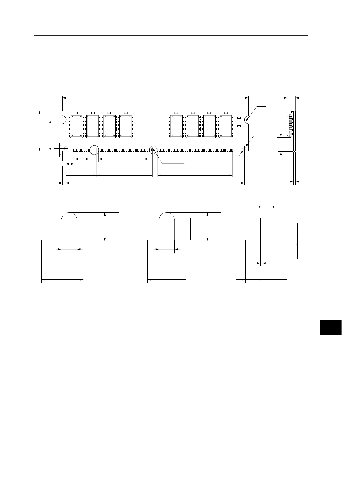
PIN CONFIGURATION
MSC23V26457TA-xxBS8
(Unit : mm)
*1
25.4 ±0.13
17.78 ±0.13
5.89 ±0.13
3.0 ±0.13
11.43 ±0.1
21.495 ±0.13
133.35 ±0.2
36.83 ±0.1
45.18 ±0.13 54.61 ±0.1
127.35 Typ.3.0 ±0.13
2 – R1 ±0.1
2 – R2 ±0.1
2 – φ3 ±0.1
84BA
6.0 Min.
2.67 Max.
1.27 ±0.1
8
CL
3.00 ±0.13
2.0 ±0.1
6.35 ±0.1
3.00 ±0.13
2.0 ±0.1
6.35 ±0.1
DETAIL BDETAIL A
*1 The common size difference of the board width 19.78 mm of its height is
specified as ±0.2. The value above 19.78 mm is specified as ±0.5.
1.0 ±0.1
0.25 Max.
0.23 Min.
1.27 ±0.1
632
MSC23V26457SA-xxBS8
25.4 ±0.13
3.0 ±0.13
17.78 ±0.13
5.89 ±0.13
11.43 ±0.1
21.495 ±0.13
MSC23V26457TA-xxBS8/MSC23V26457SA-xxBS8¡ Semiconductor
*1
133.35 ±0.2
36.83 ±0.1
45.18 ±0.13 54.61 ±0.1
127.35 Typ.3.0 ±0.13
2 – R1 ±0.1
(Unit : mm)
5.28 Max.
2 – R2 ±0.1
2 – φ3 ±0.1
84BA
6.0 Min.
1.27 ±0.1
CL
3.00 ±0.13
2.0 ±0.1
6.35 ±0.1
3.00 ±0.13
2.0 ±0.1
6.35 ±0.1
DETAIL BDETAIL A
*1 The common size difference of the board width 19.78 mm of its height is
specified as ±0.2. The value above 19.78 mm is specified as ±0.5.
1.0 ±0.1
0.25 Max.
0.23 Min.
1.27 ±0.1
8
633
MSC23V26457TA-xxBS8/MSC23V26457SA-xxBS8 ¡ Semiconductor
Front Side
Pin No.
Pin Name
11835
2 193653
3 203754
4 213855
5 223956
6 234057
7 244158
8 254259
9 264360
10 27 44 61
11 28 45 62
12 29 46 63
13 30 47 64
14 31 48 65
15 32 49 66
16 33 50 67
17 34 51 68
V
SS
DQ0 DQ14 A6 NC
DQ1 DQ15 A8 V
DQ2 NC A10R DQ16
DQ3 NC NC DQ17
V
CC
DQ4 NC V
DQ5 NC NC V
DQ6 V
DQ7 WE0 OE2 NC
DQ8 CAS0 RAS2 NC
V
SS
DQ9 RAS0 CAS3 V
DQ10 OE0 WE2 DQ21
DQ11 V
DQ12 A0 NC DQ23
DQ13 A2 NC V
Pin No.
Pin Name
V
CC
V
SS
CC
Pin No.
Pin Name
Pin No.
A4 NC
V
CC
CC
V
SS
CAS1 CAS2 NC
SS
V
CC
Pin Name52Pin No.
SS
DQ18
DQ19
CC
DQ20
SS
DQ22
SS
69
70
71
72
73
74
75
76
77
78
79
80
81
82
83
84
Pin Name
DQ24
DQ25
DQ26
DQ27
V
CC
DQ28
DQ29
DQ30
DQ31
V
SS
NC
NC
NC
SDA
SCL
V
CC
8
Back Side
Pin No.
100 117 134 151
101 118 135 152
Pin Name
85 102 119
86 103 120 137
87 104 121 138
88 105 122 139
89 106 123 140
90 107 124 141
91 108 125 142
92 109 126 143
93 110 127 144
94 111 128 145
95 112 129 146
96 113 130 147
97 114 131 148
98 115 132 149
99 116 133 150
V
SS
DQ32 DQ46 A7 NC
DQ33 DQ47 A9 V
DQ34 NC NC DQ48
DQ35 NC NC DQ49
V
CC
DQ36 NC NC DQ51
DQ37 NC NC V
DQ38 V
DQ39 NC NC NC
DQ40 CAS4 NC NC
V
SS
DQ41 NC CAS7 V
DQ42 NC NC DQ53
DQ43 V
DQ44 A1 NC DQ55
DQ45 A3 NC V
Pin No.
Pin Name
V
CC
V
SS
CC
Pin No.
Pin Name
A5 NC
V
CC
V
SS
CAS5 CAS6 NC
SS
V
CC
Pin No.
136
Pin Name
SS
DQ50
CC
DQ52
SS
DQ54
SS
Pin No.
153
154
155
156
157
158
159
160
161
162
163
164
165
166
167
168
Pin Name
DQ56
DQ57
DQ58
DQ59
V
CC
DQ60
DQ61
DQ62
DQ63
V
SS
NC
NC
SA0
SA1
SA2
V
CC
634

Serial PD Matrix
MSC23V26457TA-xxBS8/MSC23V26457SA-xxBS8¡ Semiconductor
Byte Number
0
1
2
3
4
5
6
7
8
9 (-60)
9 (-70)
10 (-60)
10 (-70)
Bit 7 Bit 6 Bit 5 Bit 4 Bit 3 Bit 2 Bit 1 Bit 0 Remark
00001101
00001000
00000010
00001011
00001010
00000001
01000000
00000000
00000010
00111100
01000110
00001111
00010100
0000000011 Non parity
0000000012 Normal Refresh
Number of Bytes used (13 Bytes)
Total SPD Memory size (256 Bytes)
Memory type (EDO)
Number of Rows (11)
Number of Columns (10)
Number of Banks (1)
Module Data Width (64)
Module Data Width Continued (0)
Supply Voltage (3.3 V, LVTTL)
RAS Access Time (60 ns)
RAS Access Time (70 ns)
CAS Access Time (15 ns)
CAS Access Time (20 ns)
635
8
MSC23V26457TA-xxBS8/MSC23V26457SA-xxBS8 ¡ Semiconductor
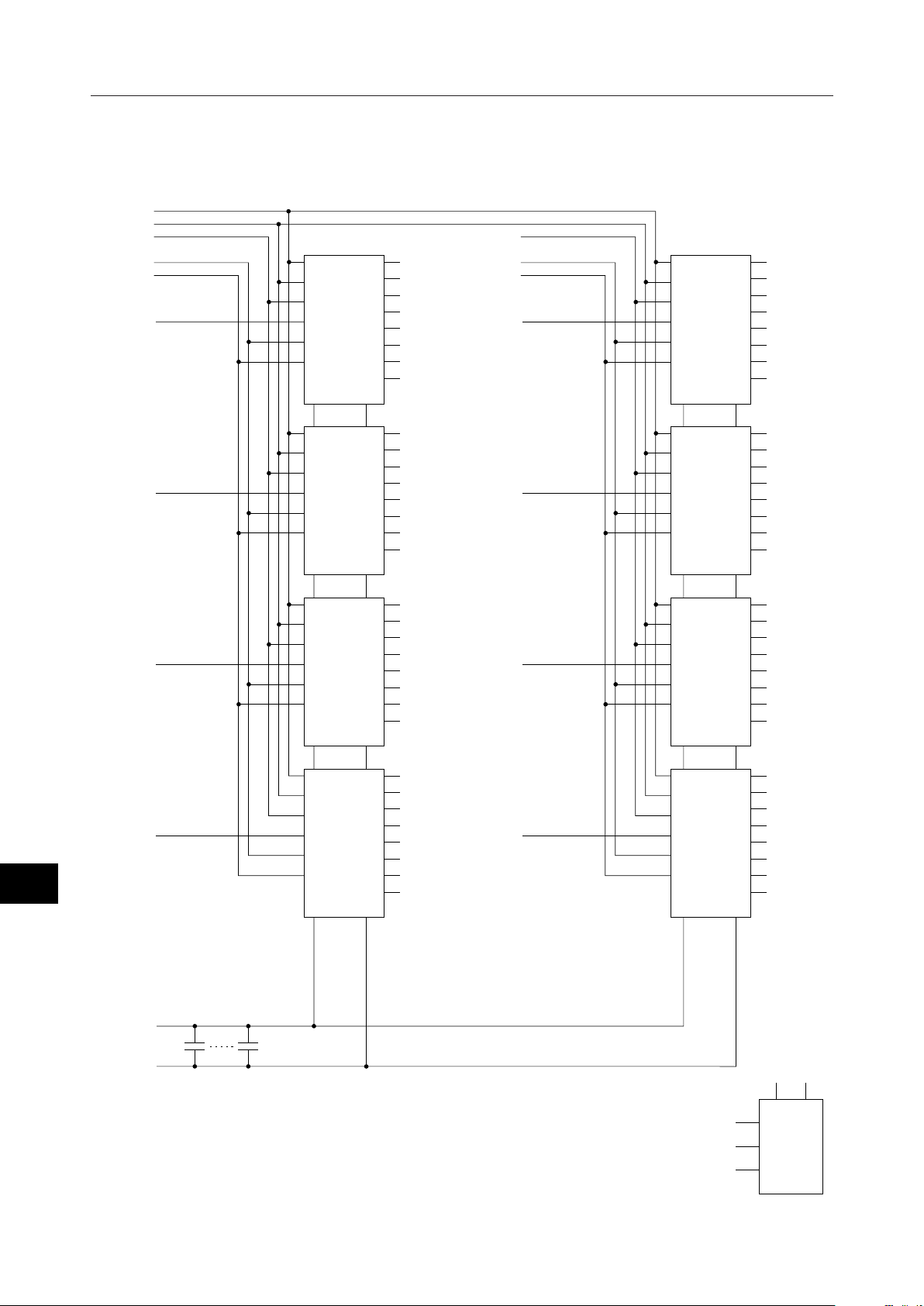
BLOCK DIAGRAM
A0 - A9
A10R
RAS0
WE0
OE0
CAS0
A0 - A9 DQ0
A10R
RAS
CAS
WE
OE
V
CC
DQ
DQ
DQ
DQ
DQ
DQ
DQ DQ6
DQ
V
SS
DQ1
DQ2
DQ3
DQ4
DQ5
DQ7
RAS2
WE2
OE2
CAS4
A0 - A9 DQ32
A10R
RAS
CAS
WE
OE
V
CC
DQ
DQ33
DQ
DQ
DQ34
DQ
DQ35
DQ
DQ36
DQ
DQ37
DQ DQ38
DQ
DQ39
V
SS
8
CAS1
CAS2
CAS3
A0 - A9 DQ8
A10R
RAS
CAS
WE
OE
V
CC
A0 - A9 DQ16
A10R
RAS
CAS
WE
OE
V
CC
A0 - A9 DQ24
A10R
RAS
CAS
WE
OE
V
CC
DQ
DQ9
DQ
DQ
DQ10
DQ
DQ11
DQ
DQ12
DQ
DQ13
DQ DQ14
DQ15
DQ
V
SS
DQ
DQ17
DQ
DQ
DQ18
DQ
DQ19
DQ
DQ20
DQ
DQ21
DQ DQ22
DQ
DQ23
V
SS
DQ
DQ25
DQ
DQ
DQ26
DQ
DQ27
DQ
DQ28
DQ
DQ29
DQ30
DQ
DQ
DQ31
V
SS
CAS5
CAS6
CAS7
A0 - A9 DQ40
A10R
RAS
CAS
WE
OE
V
CC
A0 - A9 DQ48
A10R
RAS
CAS
WE
OE
V
CC
A0 - A9 DQ56
A10R
RAS
CAS
WE
OE
V
CC
DQ
DQ41
DQ
DQ
DQ42
DQ
DQ43
DQ
DQ44
DQ
DQ45
DQ DQ46
DQ47
DQ
V
SS
DQ
DQ49
DQ
DQ
DQ50
DQ
DQ51
DQ
DQ52
DQ
DQ53
DQ DQ54
DQ
DQ55
V
SS
DQ
DQ57
DQ
DQ
DQ58
DQ
DQ59
DQ
DQ60
DQ
DQ61
DQ62
DQ
DQ
DQ63
V
SS
636
V
CC
C1 C8
V
SS
SA0
SA1
SA2
SCL SDA
SCL SDA
A0
A1
A2
Serial PD

ELECTRICAL CHARACTERISTICS
Absolute Maximum Ratings
MSC23V26457TA-xxBS8/MSC23V26457SA-xxBS8¡ Semiconductor
Parameter
Voltage on Any Pin Relative to V
Voltage VCC Supply Relative to V
SS
SS
Symbol
V
IN
V
Short Circuit Output Current I
Power Dissipation P
Operating Temperature T
Storage Temperature T
, V
OS
opr
OUT
CC
D
stg
Rating Unit
–0.5 to 4.6 V
–0.5 to 4.6 V
50 mA
8W
0 to 70 °C
–40 to 125 °C
Note: Permanent device damage may occur if ABSOLUTE MAXIMUM RATINGS are
exceeded. Functional operation should be restricted to the conditions as detailed in the
operational sections of this data sheet. Exposure to absolute maximum rating conditions
for extended periods may affect device reliability.
Recommended Operating Conditions
(Ta = 0°C to 70°C)
Parameter
Power Supply Voltage
Input High Voltage
Input Low Voltage
Symbol
V
CC
V
SS
V
IH
V
IL
Min.
Typ.
3.0 3.3 3.6 V
000V
2.0 — VCC + 0.3 V
–0.3 — 0.8 V
Max.
Unit
Capacitance
Parameter
Input Capacitance
(RAS0, RAS2,
WE0, WE2, OE0, OE2)
Input Capacitance (CAS0 - CAS7)
Symbol
C
IN1
C
IN2
C
IN3
C
DQ
Typ.
Note : Capacitance measured with Boonton Meter.
(Ta = 25°C, f = 1 MHz)
Max.
—49
—35
—13
Unit
pFInput Capacitance (A0 - A9, A10R)
pF
pF
pFI/O Capacitance (DQ0 - DQ63) — 13
8
637

MSC23V26457TA-xxBS8/MSC23V26457SA-xxBS8 ¡ Semiconductor
DC Characteristics
(VCC = 3.3 V ±0.3 V, Ta = 0°C to 70°C)
Parameter
Input Leakage Current
Output Leakage Current
Output High Voltage
Output Low Voltage
Average Power
Supply Current
(Operating)
Power Supply
Current (Standby)
Average Power
Supply Current
(RAS-only Refresh)
Average Power
Supply Current
(CAS before RAS Refresh)
Average Power
Supply Current
(Fast Page Mode)
Symbol
I
LI
I
LO
V
OH
V
OL
I
CC1
I
CC2
I
CC3
I
CC6
I
CC7
Condition
0 V £ VI £ VCC + 0.3 V;
All other pins not
under test = 0 V
disable
D
OUT
0 V £ V
I
OH
I
OL
£ 3.6 V
O
= –2.0 mA
= 2.0 mA
RAS, CAS cycling,
= Min.
t
RC
RAS, CAS = V
IH
RAS, CAS
≥ V
–0.2 V
CC
RAS cycling,
= Min.
,
IH
CAS = V
t
RC
RAS cycling,
CAS before RAS,
= Min.
t
RC
RAS = V
,
IL
CAS cycling,
= Min.
t
HPC
-60 -70
Min.
–80
Max.
80
CC
Min.
–80
2.4 V
Max.
80
CC
Unit
µA
µA–10 10 –10 10
V2.4 V
V0 0.4 0 0.4
mA— 1200 — 1040
mA—16—16
mA—8—8
mA— 1200 — 1040
mA— 1200 — 1040
mA— 1200 — 1040
Note
1, 2
1
1
1, 2
1, 2
1, 3
8
Notes: 1. ICC Max. is specified as ICC for output open condition.
2. Address can be changed once or less while RAS=VIL.
3. Address can be changed once or less while CAS=VIH.
638

AC Characteristics (1/2)
MSC23V26457TA-xxBS8/MSC23V26457SA-xxBS8¡ Semiconductor
(V
= 3.3 V ±0.3 V, Ta = 0°C to 70°C) Note 1,2,3,12,13
CC
Parameter
Symbol
Random Read or Write Cycle Time
Read Modify Write Cycle Time t
Fast Page Mode Cycle Time t
Fast Page Mode Read Modify Write Cycle Time
t
PRWC
Access Time from RAS t
Access Time from CAS t
Access Time from Column Address t
Access Time from CAS Precharge t
Access Time from OE t
Output Low Impedance Time from CAS t
Output Hold Time from CAS Low t
CAS to Data Output Buffer Turn-off Delay Time
RAS to Data Output Buffer Turn-off Delay Time
OE to Data Output Buffer Turn-off Delay Time
WE to Data Output Buffer Turn-off Delay Time
t
Transition Time t
Refresh Period t
RAS Precharge Time t
RAS Pulse Width t
RAS Pulse Width (Fast Page Mode) t
RAS Hold Time t
RAS Hold Time referenced to OE t
CAS Precharge Time t
CAS Pulse Width t
RAS Low to CAS High Delay Time t
CAS High to RAS Low Delay Time t
RAS Hold Time from CAS Precharge t
CAS, OE Hold Time (Output Disable) t
RAS to CAS Delay Time t
RAS to Column Address Delay Time t
RAS to Second CAS Delay Time t
Row Address Set-up Time t
Row Address Hold Time t
Column Address Set-up Time t
Column Address Hold Time t
Column Address Hold Time from RAS t
Column Address to RAS Lead Time t
t
RC
RWC
HPC
RAC
CAC
AA
CPA
OEA
CLZ
DOH
t
CEZ
t
REZ
t
OEZ
WEZ
T
REF
RP
RAS
RASP
RSH
ROH
CP
CAS
CSH
CRP
RHCP
CHO
RCD
RAD
RSCD
ASR
RAH
ASC
CAH
AR
RAL
Min.
110
150
25
80
—
—
—
—
0
0
3
—
40
60
60
15
10
15
40
5
35
20
15
0
10
0
15
40
30
-60
Max.
—
—
—
—
60
15
30
35
—
15
50
32
—
10k
100k
—
—
10k
—
—
—
45
30
—
—
—
—
—
—
Min.
130
180
30
95
—
—
—
—
0
0
3
—
50
70
70
20
10
20
45
5
40
20
15
0
10
0
15
45
35
-70
Max.
—
—
—
—
70
20
35
40
—
15
50
32
—
10k
100k
—
—
10k
—
—
—
50
35
—
—
—
—
—
—
Unit
ns
ns
ns
ns
ns
ns
ns
ns
ns 4—20—15
ns
ns5—5—
ns
ns 7, 8015015
ns 7015015
ns 7015015
ns
ms
ns
ns
ns
ns
ns20 —15 —
ns
ns
ns
ns
ns
ns10 —5—
ns
ns
ns70 —60 —
ns
ns
ns
ns
ns
ns
Note
4, 5, 6
4, 5
4, 6
4
4
7, 8
3
8
5
6
639

MSC23V26457TA-xxBS8/MSC23V26457SA-xxBS8 ¡ Semiconductor
AC Characteristics (2/2)
(VCC = 3.3 V ±0.3 V, Ta = 0°C to 70°C) Note 1,2,3,12,13
8
Parameter
Read Command Set-up Time
Read Command Hold Time
Read Command Hold Time referenced to RAS
Write Command Set-up Time
Write Command Hold Time
Write Command Hold Time from RAS
Write Command Pulse Width
Write Command Pulse Width (Output Disable)
WE Low to OE Low Delay Time
OE Precharge Time
OE Low to CAS High Delay Time
Write Command to RAS Lead Time
Write Command to CAS Lead Time
Data-in Set-up Time
Data-in Hold Time
Data-in Hold Time from RAS
OE
to Data-in Delay Time ns
CAS
to WE Delay Time ns
Column Address to WE Delay Time ns
RAS to WE Delay Time ns
CAS
Precharge to WE Delay Time ns
CAS Active Delay Time from RAS Precharge
RAS to CAS Set-up Time (CAS before RAS)
RAS to CAS Hold Time (CAS before RAS)ns
WE to RAS Precharge Time (CAS before RAS)
WE Hold Time from RAS (CAS before RAS)
RAS to WE Set-up Time (Test Mode)
RAS to WE Hold Time (Test Mode)
Symbol
RCS
t
RCH
t
RRH
t
WCS
t
WCH
t
WCR
t
WP
t
WPE
t
OEH
t
OEP
t
OCH
t
RWL
t
CWL
t
DS
t
DH
t
DHR
t
OED
t
CWD
t
AWD
t
RWD
t
CPWD
t
RPC
t
CSR
t
CHR
t
WRP
t
WRH
t
WTS
t
WTH
Min.
0
0
0
0
10
40
10
15
15
0
15
40
5
5
10
Max.
—
—
—
—
—
—
—
—
—
—
—
—
—
—
—
-60
-70
Min.
0
0
0
0
15
45
15
Max.
—t
—
—
—
—
—
—
Unit
ns
ns
ns
ns
ns
ns
ns
ns10 —5—
ns20 —15 —
ns10 —10 —
ns10 —10 —
20
20
15
45
—
—
0
—
—
—
ns
ns
ns
ns
ns
15 —15 —
45 —35 —
60 —50 —
95 —80 —
65 —55 — 10
ns
ns
15
5
5
—
—
—
ns10 —10 —
ns10 —10 —
ns10 —10 —
ns10 —10 —
Note
9
9
10
11
11
10
10
10
640

MSC23V26457TA-xxBS8/MSC23V26457SA-xxBS8¡ Semiconductor
Notes: 1. A start-up delay of 200 µs is required after power-up, followed by a minimum of eight
initialization cycles (RAS-only refresh or CAS before RAS refresh) before proper device
operation is achieved.
2. The AC characteristics assume tT = 5 ns.
3. VIH (Min.) and VIL (Max.) are reference levels for measuring input timing signals.
Transition times (tT) are measured between VIH and VIL.
4. This parameter is measured with a load circuit equivalent to 2 TTL loads and 100 pF.
5. Operation within the t
t
(Max.) is specified as a reference point only. If t
RCD
t
(Max.) limit, access time is controlled by t
RCD
6. Operation within the t
t
(Max.) is specified as a reference point only. If t
RAD
t
(Max.) limit, access time is controlled by tAA.
RAD
7. t
(Max.), t
CEZ
REZ
(Max.), t
(Max.) limit ensures that t
RCD
(Max.) limit ensures that t
RAD
(Max.) and t
WEZ
(Max.) can be met.
RAC
is greater than the specified
RCD
.
CAC
(Max.) can be met.
RAC
is greater than the specified
RAD
(Max.) define the time at which the
OEZ
output achieves the open circuit condition and are not referenced to output voltage
levels.
8. t
9. t
10. t
CEZ
RCH
WCS
and t
or t
, t
CWD
must be satisfied for open circuit condition.
REZ
must be satisfied for a read cycle.
RRH
, t
RWD
, t
AWD
and t
are not restrictive operating parameters. They
CPWD
are included in the data sheet as electrical characteristics only. If t
WCS
≥ t
WCS
(Min.)
the cycle is an early write cycle and the data output pin will remain in a high
impedance state throughout the entire cycle. If t
(Min.), t
AWD
≥ t
(Min.) and t
AWD
CPWD
≥ t
CPWD
CWD
≥ t
CWD
(Min.), t
RWD
≥ t
RWD
(Min.), the cycle is a read modify
write cycle and the data output pin will contain data read from the selected cell. If
neither conditions is satisfied, the data output logic state (at access time) is
undefined.
11. These parameters are referenced to CAS leading edge in an early write cycle and to
WE leading edge in an OE control write cycle or a read modify write cycle.
8
12. The test mode is initiated by performing a WE and CAS before RAS refresh cycle.
This mode is latched and remains in effect until the exit cycle is generated.
In the test mode CA9 is not used and each DQ pin now accesses 2 bit locations. In
a read cycle, if the 2 data bits are equal, the DQ pin will indicate a high level. If the
2 data bits are not equal, the DQ pin will indicate a low level.
The test mode is cleared and the memory device returned to its normal operating
state by performing a RAS-only refresh cycle or a CAS before RAS refresh cycle.
13. In a test mode read cycle, the access time parameters are delayed by 5 ns. The test
mode parameters are obtained by adding 5 ns to the normal read cycle values.
See ADDENDUM K for AC Timing Waveforms
641
 Loading...