

Page 1

PEDL9040A-03
¡ Semiconductor
PEDL9040A-03
This version: Oct. 2000
Previous version: Sep. 2000
ML9040A-Axx/-Bxx¡ Semiconductor
Preliminary
ML9040A-Axx/-Bxx
DOT MATRIX LCD CONTROLLER WITH 16-DOT COMMON DRIVER AND 40-DOT
SEGMENT DRIVER
GENERAL DESCRIPTION
The ML9040A-Axx/-Bxx is a dot matrix LCD controller which is fabricated in low power CMOS
silicon gate technology. Character display on the dot matrix character type LCD can be
controlled in combination with a 4-bit or 8-bit microcontroller. This LSI consists of 16-dot
COMMON driver, 40-dot SEGMENT driver, display data RAM, character generator RAM,
character generator ROM and control circuit.
The ML9040A-Axx/-Bxx has the character generator ROM that can be programmed by custom
mask. The ML9040A-A01/-B01 is a standard version having 160 characters with lowercase (5
x 7 dots), and 32 characters with uppercase (5 x 10 dots) in this ROM.
FEATURES
• Easy interface with an 8-bit or 4-bit microcontroller.
• Dot matrix LCD controller/driver for lowercase (5 x 7 dots) or uppercase (5 x 10 dots).
• Automatic power ON reset.
• COMMON signal drivers (16) and SEGMENT signal drivers (40).
• Can control up to 80 characters when used in combination with MSM5259.
• Character generator ROM for 160 characters with lowercase (5 x 7 dots) and 32 characters with
uppercase (5 x 10 dots).
• Character patterns are programmable by character generator RAM. (Lowercase: 5 x 8 dots,
8 patterns, uppercase: 5 x 11 dots, 4 patterns).
• Built-in oscillation circuit to connect with external resistor or ceralock.
• 1/8 duty (1 line; 5 x 7 dots + cursor), 1/11 duty (1 line; 5 x 10 dots + cursor), or 1/16 duty (2
lines; 5 x 7 dots + cursor), selectable.
• Clear display even at 1/5 bias, 3.0V LCD driving voltage.
• LCD driving waveform
ML9040A-Axx: A mode
ML9040A-Bxx: B mode
• Package options:
80-pin plastic QFP(QFP80-P-1420-0.80-BK)(Product name: ML9040A-Axx/-BxxGA)
Al pad chip (Product name: ML9040A-Axx/-BxxWA)
xx indicates code number.
01 indicates standard code number.
1/49
Page 2
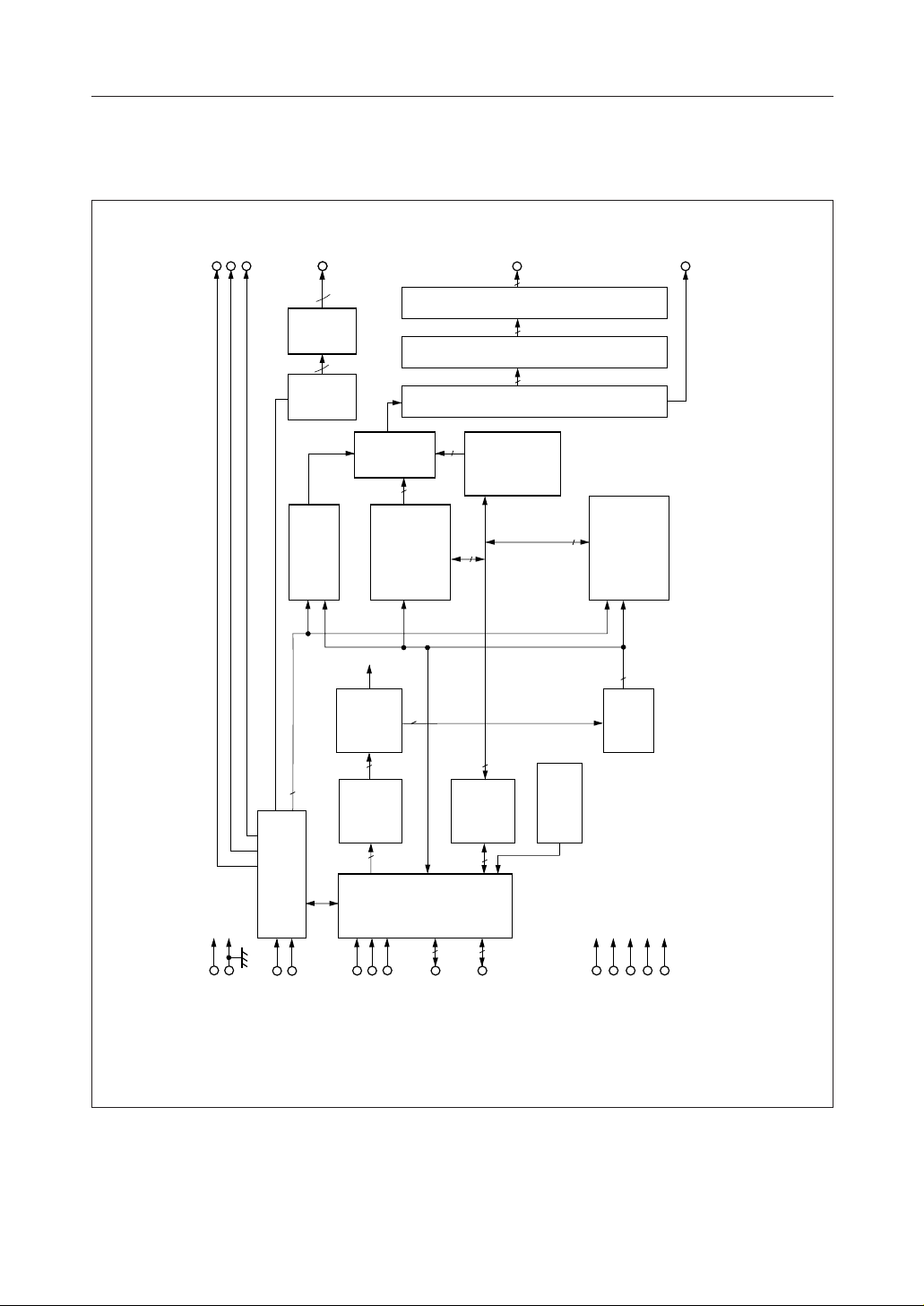
BLOCK DIAGRAM
PEDL9040A-03
ML9040A-Axx/-Bxx¡ Semiconductor
L
CP
DF
1~16
COM
16
Common
signal
driver
16
16-bit
shift
register
Cursor blink
control
7
Parallel/
Instruction
decoder
(ID)
8
serial
conver-
sion
55
Character
generator
RAM
5
8
(CG RAM)
7
8
40
Seg-
4040
40-bit
40-bit
Character
generator
ROM
SEG
ment
signal
latch
shift
register
(CG RAM)
1~40
driver
DO
8
Display data
RAM
(DD RAM)
77
Address
counter
(ADC)
Data
register
3
- DB
0
DB
8
4
(DR)
7
- DB
4
DB
Busy flag
(BF)
1
V
V2V3V4V
5
Instruction
register
(IR)
8
Timing
generation
circuit
Input/
output
buffer
4
1
2
DD
V
GND
OSC
OSC
ERSR/W
2/49
Page 3
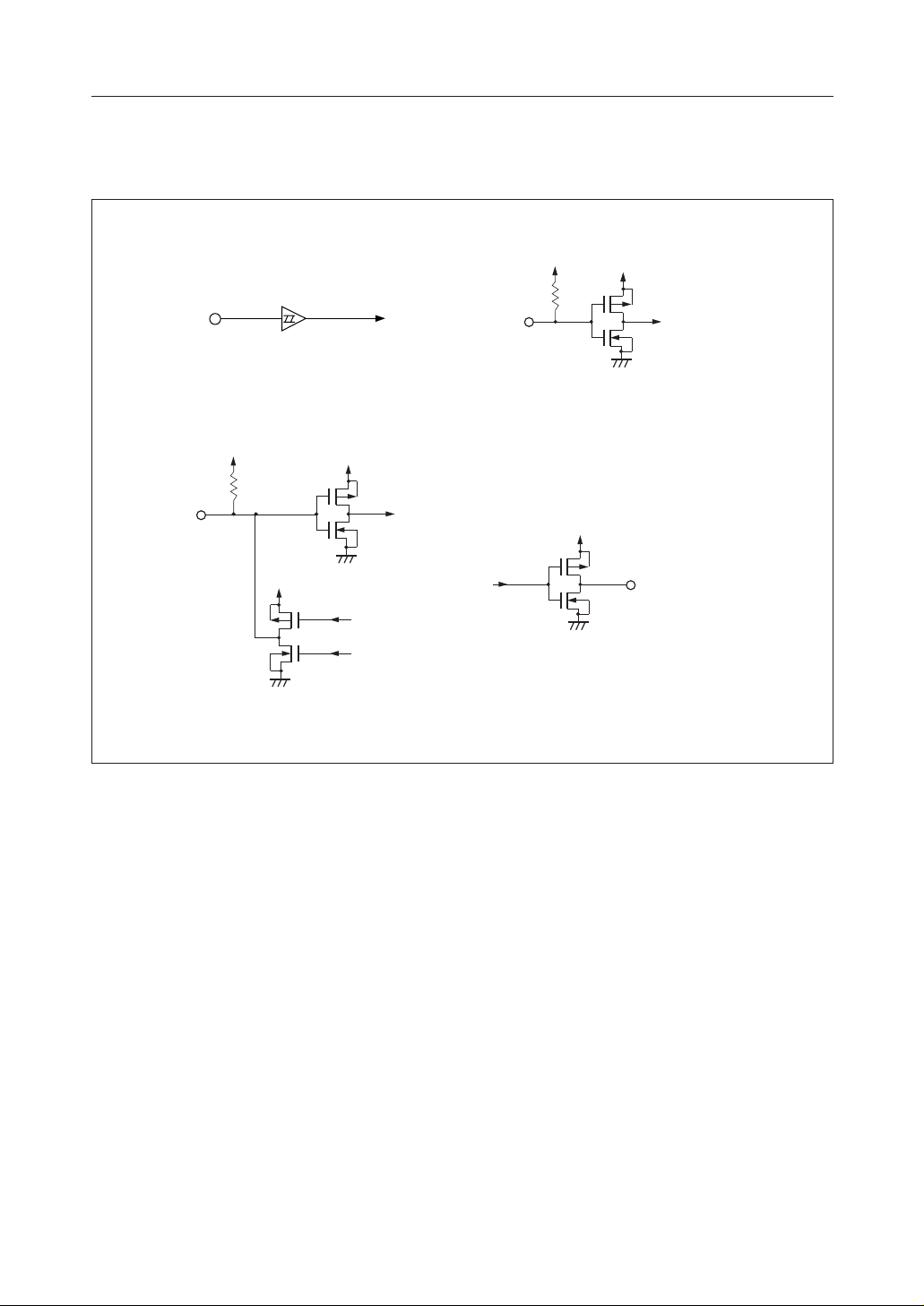
INPUT AND OUTPUT CONFIGURATION
PEDL9040A-03
ML9040A-Axx/-Bxx¡ Semiconductor
V
DD
V
DD
P
N
Applicable to pin E.
V
DD
V
DD
P
N
Applicable to pins DB
V
DD
- DB7.
0
Applicable to pins R/W and RS.
P
V
DD
N
P
N
Applicable to pins DO, CP, L, and DF.
3/49
Page 4
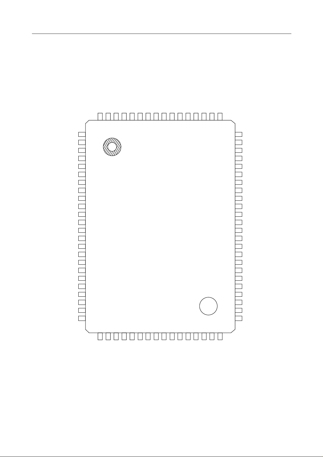
PIN CONFIGURATION (TOP VIEW)
ML9040A-Axx/-Bxx GA
27
26
25
23
24
SEG
SEG
SEG
SEG
SEG
80
79
76
77
78
28
SEG
75
29
SEG
74
30
SEG
73
31
SEG
72
32
SEG
71
33
SEG
70
34
SEG
69
35
SEG
68
36
SEG
67
37
SEG
66
PEDL9040A-03
ML9040A-Axx/-Bxx¡ Semiconductor
38
SEG
65
SEG
SEG
SEG
SEG
SEG
SEG
SEG
SEG
SEG
SEG
SEG
SEG
SEG
SEG
SEG
SEG
SEG
SEG
SEG
SEG
SEG
SEG
GND
OSC
1
22
2
21
3
20
4
19
5
18
6
17
7
16
8
15
9
14
10
13
11
12
12
11
13
10
14
9
15
8
16
7
17
6
18
5
19
4
20
3
21
2
22
1
23
24
1
64
SEG
39
63
SEG
40
62
COM
16
61
COM
15
60
COM
14
59
COM
13
58
COM
12
57
COM
11
56
COM
10
55
COM
9
54
COM
COM
COM
COM
COM
COM
COM
COM
DB
DB
DB
DB
DB
DB
8
7
6
5
4
3
2
1
7
6
5
4
3
2
53
52
51
50
49
48
47
46
45
44
43
42
41
25
2
OSC
32L31
CP
33
DD
V
35DF34
DO
37RS36
R/W
26
2
1
V
V
5
4
3
V
V
V
30
29
28
27
40
39
38
1
0
E
DB
DB
80-Pin Plastic QFP
4/49
Page 5
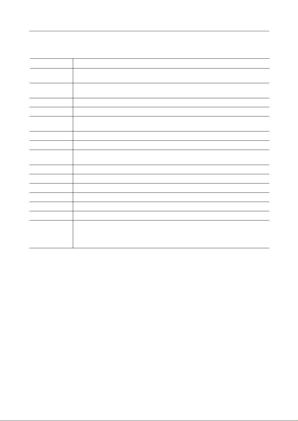
PIN DESCRIPTIONS
PEDL9040A-03
ML9040A-Axx/-Bxx¡ Semiconductor
Symbol
Description
R/W Read/write selection input pin.
"H" : Read, and "L" : Write
RS Register selection input pin.
"H" : Data register, and "L" : Instruction register
E Input pin for data input/output with CPU and for instruction register activation.
DB0 - DB
OSC1, OSC
7
2
Input/output pins for data send/receive with CPU
Clock oscillating pins required for internal operation upon receipt of the LCD drive signal
and CPU instruction.
COM1 - COM
SEG1 - SEG
16
40
LCD COMMON signal output pins.
LCD SEGMENT signal output pins.
DO Output pin to be connected to MSM5259 to expand the number of characters to be
displayed.
CP Clock output pin used when DO pin data output shifts inside of MSM5259.
L Clock output pin for the serially transferred data to be latched to MSM5259.
DF The alternating current signal (Display Frequency) output pin.
V
DD
GND
Power supply pin.
Ground pin.
V1, V2, V3, V4, V5Bias voltage input pins to drive the LCD.
TEST
This is the pin for testing the IC chip.
Leave this pin open during normal use.
*This pin is available only for Al pad chip.
5/49
Page 6
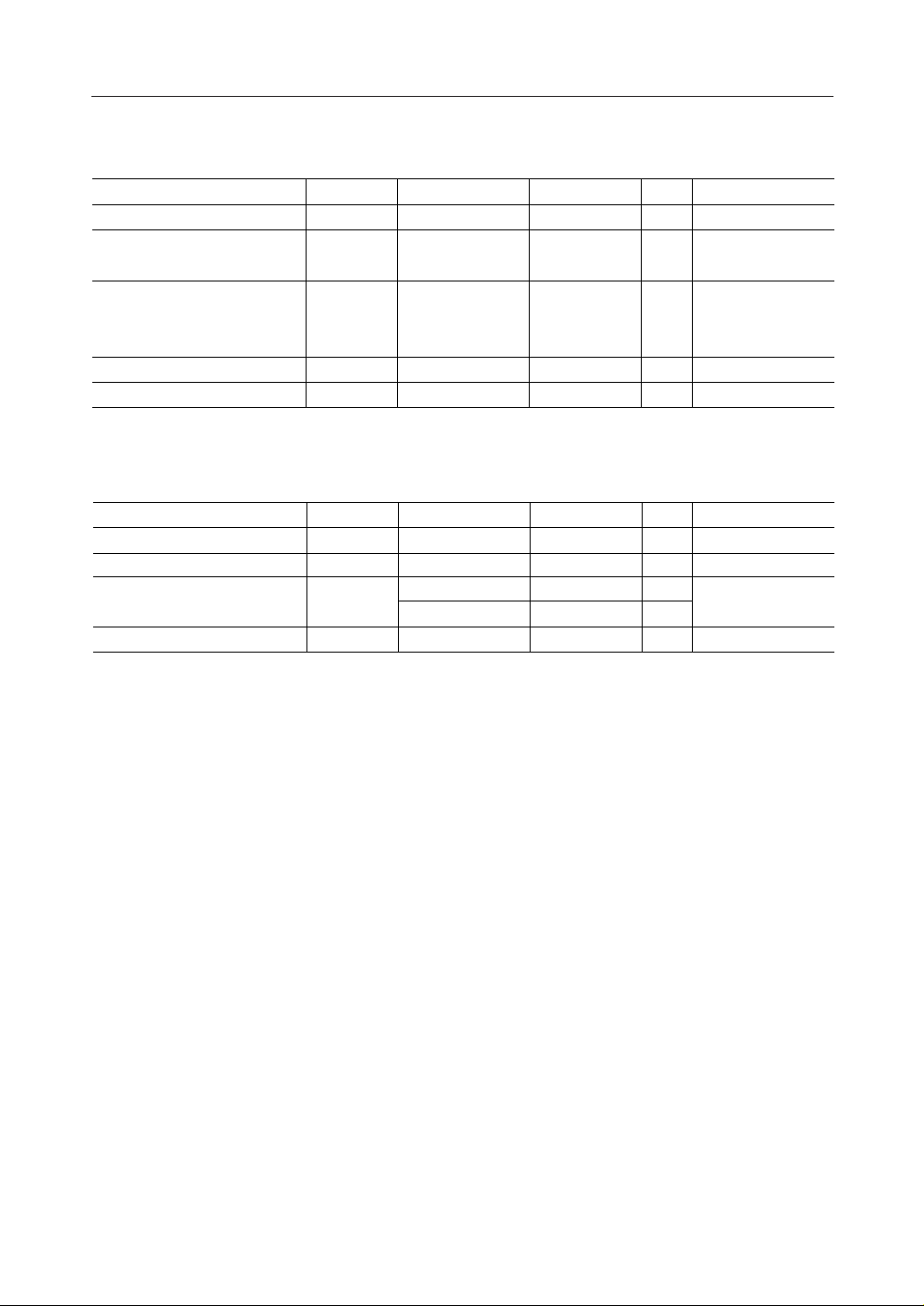
ABSOLUTE MAXIMUM RATINGS
PEDL9040A-03
ML9040A-Axx/-Bxx¡ Semiconductor
Parameter
Supply Voltage
LCD Driving Voltage
Input Voltage V
Power Dissipation P
Storage Temperature T
Symbol Condition Rating Unit Applicable pin
Ta = 25°C –0.3 to + 7.0 V V
V
Ta = 25°C
DD
V
DD
Ta = 25°C –0.3 to V
— 500 mW —
— –55 to + 150 °C—
V
1
V
DD
, V2, V
V4, V
I
D
STG
3
5
RECOMMENDED OPERATING CONDITIONS
Parameter
Supply Voltage
Data Holding Voltage
LCD Driving Voltage
*1
*2
Operating Temperature T
*1 Voltage to assure Rf oscillation and register data retention.
*2 Voltage between VDD and V
*3 Voltages applicable to V1, V2, V3 and V4 are as follows.
V1 = VDD – 1/4 (VDD – V5)
V2 = V3 = VDD – 1/2 (VDD - V5)
V4 = VDD – 3/4 (VDD – V5)
*4 V1 = VDD – 1/5 (VDD – V5)
V2 = VDD – 2/5 (VDD – V5)
V3 = VDD – 3/5 (VDD – V5)
V4 = VDD – 4/5 (VDD – V5)
Symbol Condition Range Unit Applicable pin
— 4.5 to 5.5 V VDD, GND
— 3.0 to 5.5 V VDD, GND
1/4 bias, VDD–V
1/5 bias, VDD–V
*3
3.0 to 6.0 V
5
*4
3.0 to 6.0 V
5
— –20 to + 75 °C—
V
V
HOLD
V
LCD
5.
DD
op
– 8.0 to
+ 0.3
DD
+ 0.3 V
, GND
DD
, V2, V
V
1
V
V4, V
3
5
R/W, RS, E,
DB
- DB
0
7
OSC
1
V
, V
DD
5
6/49
Page 7
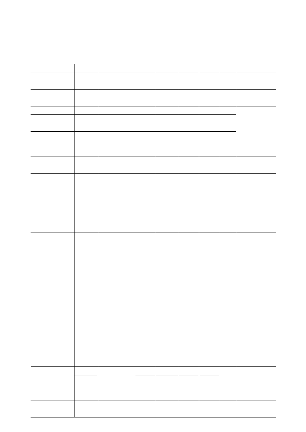
ELECTRICAL CHARACTERISTICS
DC Characteristics
Parameter
"H" Input Voltage
"L" Input Voltage V
"H" Input Voltage V
"L" Input Voltage V
"H" Output Voltage V
"L" Output Voltage V
"H" Output Voltage V
"L" Output Voltage V
Driver ON Resistor
(COM pins)
Driver ON Resistor
(SEG pins)
Input Leakage Current
Input Current I
Supply Current (1) I
Supply Current (2) I
LCD Driving Bias
Input Voltage
Schmitt voltage
width
Built-in reset
detection voltage
Symbol Condition Min. Typ. Max. Unit Applicable pin
V
IH1
IL1
IH2
IL2
OH1
OL1
OH2
OL2
R
R
COM
SEG
I
IO = ±50mA, V
IO = ±50mA, V
IL
— 2.2 — V
— –0.3 — 0.6 V
—V
— –0.3 — 1.0 V
IO = –0.205mA 2.4 — — V
IO = 1.2mA — — 0.4 V
IO = –40mA 0.9V
IO = 40mA — — 0.1V
VI = V
SS
V
= V
I
DD
VDD = 5.0V
= V
V
I
SS
VI = VDD, excluding current
IL2
flowing over pullup resistor
and output drive MOS
= 5.0V,
V
DD
resistor oscillation or
external clock input via
.
OSC
1
= 270kHz.
f
DD1
OSC
E is in "L" level.
Other inputs are open.
Output pins are
all no load. *1
VDD = 5.0V,
ceramic oscillation,
= 250kHz.
f
OSC
E is in "L" level.
DD2
Other pins are open.
Output pins are
all no load. *1
V
V
V
V
LCD1
V
LCD2
SUM
RES
DD–V5
——— 0.6
——— — — 3.0 V V
*6
PEDL9040A-03
ML9040A-Axx/-Bxx¡ Semiconductor
(V
= 4.5 to 5.5V, Ta = –20 to +75°C)
DD
DD
–1.0 — V
DD
— — V DO, CP, L,
DD
= 4V — — 20 kW COM1 - COM
LCD
= 4V — — 30 kW SEG1 - SEG
LCD
DD
——–1mA
——1mA
–50 –125 –250 mA
——2mA
— 0.35 0.6 mA
— 0.55 0.8 mA
1/5 bias — 6.0
1/4 bias — 6.0
3.0
3.0
0.7 0.8 V E
V RS, E, DB0 - DB
DB0 - DB7, RS, E, R/W
V OSC1, R/W
V
DD
V
DB
DF, OSC
R/W, RS
DB
VDD, V1, V2,
V
3
OSC
1
- DB
0
E
- DB
0
V
DD
V
DD
, V4, V
DD
7
7
2
16
40
7
5
7/49
Page 8
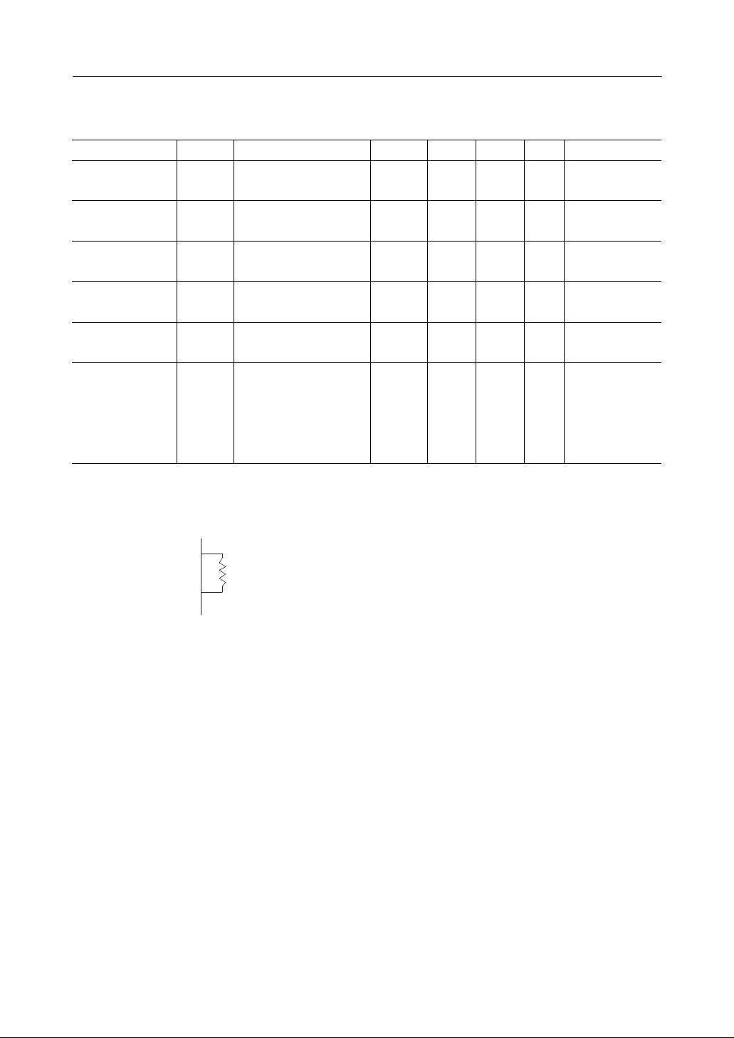
AC Characteristics
Parameter
Clock Oscillation
R
f
Frequency
Clock Input
Frequency
Symbol Condition Min. Typ. Max. Unit Applicable pin
f
OSC1
f
Rf = 91kW ± 2%
*2
OSC2 is open.
IN
Input from OSC
PEDL9040A-03
ML9040A-Axx/-Bxx¡ Semiconductor
= 4.5 to 5.5V, Ta = –20 to +75°C)
(V
DD
OSC
190 270 350 kHz
125 250 350 kHz OSC
1
OSC
1
2
1
Input Clock Duty f
Input Clock Rise
Time
Input Clock Fall
Time
Ceramic Unit
Oscillation
Frequency
DUTY
t
t
f
OSC
r
f
= 510kW,
R
f
= C2 = 200 pF,
C
1
= 30kW, and
R
d
Ceralock CSB250A.
*3
*4
*4
45 50 55 % OSC
— — 0.2 ms OSC
— — 0.2 ms OSC
245 250 255 kHz
*5
*1 Applicable to the current that flows in pin VDD when power is input as follows:
VDD = 5V, GND = 0V, V1 = 3.8V, V2 = 2.6V, V3 = 1.4V, V4 = 0.2V, and V5 = -1V.
*2
OSC
1
R
=91kW±2%
f
Minimum wiring is required between
and Rf and between OSC2 and Rf.
OSC
1
OSC
R
f
2
OSC
OSC
1
1
1
1
2
8/49
Page 9
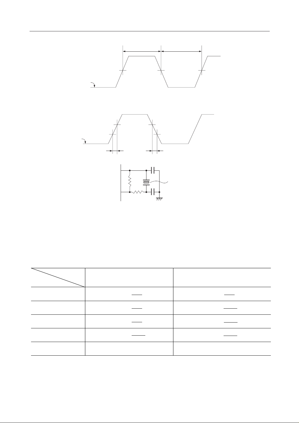
PEDL9040A-03
ML9040A-Axx/-Bxx¡ Semiconductor
*3 Applied to pulse input via OSC
0.5V
f
IN
waveform
*4 Applied to pulse input via OSC
VDD–1.0V
fIN
waveform
*5
OSC
OSC
Ceralock : CSB250A (mfd. by MURATA MFG.Co.)
Please contact us when using this circuit.
.
1
DD
.
1
t
r
1
2
R
: 510kW ±5%
f
: 30kW ±5%
R
d
: 200pF ±10%
C
1
: 200pF ±10%
C
2
t
HW
0.5V
DD
f
= tHW/ (tHW + tLW) x 100(%)
DUTY
–1.0V
V
DD
1.0V1.0V
t
f
C
1
R
f
R
d
C
2
Ceralock
t
LW
0.5V
DD
*6 Input the voltage listed in the table below to V1 - V5:
N (LCD lines)
1-line mode 2-line mode
Pin
V
V
1
V
2
V
3
V
4
V
5
V
is an LCD driving voltage. (For "N" (number of LCD lines),
LCD
V
V
V
V
V
DD
DD
DD
DD
DD
–
–
–
–
– V
V
V
3V
LCD
LCD
4
LCD
2
LCD
2
LCD
4
refer to the initial set of the instruction code.)
V
LCD
–
V
DD
5
2V
LCD
–
V
DD
V
V
DD
V
DD
DD
–
–
– V
3V
4V
LCD
5
LCD
5
LCD
5
9/49
Page 10
Switching Characteristics
PEDL9040A-03
ML9040A-Axx/-Bxx¡ Semiconductor
• Timing for input from the CPU
Parameter
R/W and RS setup time
E "H" pulse width t
R/W and RS hold time t
E rise time t
E fall time t
E "L" pulse width t
E cycle time t
to DB7 input data setup time t
DB
0
to DB7 input data hold time t
DB
0
DB
0
- DB
R/W
RS
E
7
V
IL1
V
IH1
V
IL1
t
B
V
V
t
r
IH1
IL1
V
IH1
V
IL1
= 4.5 to 5.5V, Ta = –20 to +75°C)
(V
DD
Symbol Min. Typ. Max. Unit
t
B
W
A
r
f
L
C
I
H
t
W
t
I
Input data
V
IH1
t
f
140 — — ns
280 — — ns
10—— ns
— — 100 ns
— — 100 ns
280 — — ns
667 — — ns
180 — — ns
10—— ns
V
IL1
V
IH1
V
IL1
t
A
t
L
V
IL1
t
H
V
IH1
V
IL1
V
IL1
t
C
10/49
Page 11

• Timing for output to the CPU
Parameter
R/W and RS setup time
E "H" pulse width t
R/W and RS hold time t
E rise time t
E fall time t
E "L" pulse width t
E cycle time t
to DB7 data output delay time t
DB
0
to DB7 data output hold time t
DB
0
PEDL9040A-03
ML9040A-Axx/-Bxx¡ Semiconductor
(V
= 4.5 to 5.5V, Ta = –20 to +75°C)
DD
Symbol Min. Typ. Max. Unit
t
B
W
A
r
f
L
C
D
O
140 — — ns
280 — — ns
10 — — ns
— — 100 ns
— — 100 ns
280 — — ns
667 — — ns
— — 220 ns
20 — — ns
R/W
DB0-DB
RS
V
IH2
V
IH1
V
IL1
IH1
t
W
t
D
V
OH1
Output data
V
OL1
t
B
V
V
E
7
IL1
t
r
V
IH2
V
IH1
V
IL1
t
A
t
L
V
IH1
V
IL1
t
f
t
O
V
OH1
V
OL1
t
C
V
IL1
11/49
Page 12
• Timing for output to MSM5259
Parameter
CP "H" pulse width
CP "L" pulse width t
DO setup time t
DO holding time t
"L" clock set-up time t
"L" clock hold time t
"L" "H" pulse width t
DF delay time t
PEDL9040A-03
ML9040A-Axx/-Bxx¡ Semiconductor
= 4.5 to 5.5V, Ta = –20 to +75°C)
(V
DD
Symbol Min. Typ. Max. Unit
t
HW1
LW
S
DH
SU
HO
HW2
M
800 — — ns
800 — — ns
300 — — ns
300 — — ns
500 — — ns
100 — — ns
800 — — ns
–1000 — 1000 ns
DO
CP
DF
V
OH2
V
OL2
t
t
HW1
V
OH2VOH2
t
LW
V
OL2
s
V
OH2
V
OL2
V
OH2
L
V
OH2
V
OL2
t
DH
V
V
OL2
t
SU
V
OH2
t
HW2
t
HO
V
OL2
t
M
V
OH2
OH2
12/49
Page 13
PEDL9040A-03
ML9040A-Axx/-Bxx¡ Semiconductor
FUNCTIONAL DESCRIPTION
Instruction Register (IR) and Data Register (DR)
These two registers are selected by the REGISTER SELECTION (RS) pin.
The DR is selected when the "H" level is input to the RS pin and IR is selected when the "L"
level is input.
The IR is used to store the address of the display data RAM (DD RAM) or character
generator RAM (CG RAM) and instruction code.
The IR can be written, but not be read by the microcomputer (CPU).
The DR is used to write and read the data to and from the DD RAM or CG RAM.
The data written to DR by the CPU is automatically written to the DD RAM or CG RAM
as an internal operation.
When an address code is written to IR, the data (of the specified address) is automatically
transferred from the DD RAM or CG RAM to the DR. Next, when the CPU reads the DR,
it is possible to verify DD RAM or CG RAM data from the DR data.
After the writing of DR by the CPU, the next adress in the DD RAM or CG RAM is selected
to be ready for the next CPU writing.
Likewise, after the reading out of DR by the CPU, DD RAM or CG RAM data is read out
by the DR to be ready for the next CPU reading.
Write/read to and from both registers is carried out by the READ/WRITE (R/W) pin.
Table 1 RS and R/W pins functions
R/W
L
H L Read of busy flag (BF) and address counter (ADC)
L H DR write
H H DR read
RS Function
L IR write
Busy Flag (BF)
When the busy flag is at "H", it indicates that the ML9040A-Axx/-Bxx is engaged in internal
operation.
When the busy flag is at "H", any new instruction is ignored.
When R/W = "H" and RS = "L", the busy flag is output from DB7.
New instruction should be input when busy flag is "L" level.
When the busy flag is at "H", the output code of the address counter (ADC) is undefined.
Address Counter (ADC)
The address counter (ADC) allocates the address for the DD RAM and CG RAM write/
read and also for the cursor display.
When the instruction code for a DD RAM address or CG RAM address setting is input to
IR, after deciding whether it is DD RAM or CG RAM, the address code is transferred from
IR to ADC. After writing (reading) the display data to (from) the DD RAM or CG RAM,
the ADC is incremented (decremented) by 1 internally.
The data of the ADC is output to DB0 - DB6 on the conditions that R/W = "H", RS = "L", and
BF = "L".
13/49
Page 14
PEDL9040A-03
ML9040A-Axx/-Bxx¡ Semiconductor
Timing Generator Circuit
This circuit is used to generate timing signals to activate internal operations upon receipt
of CPU instruction and also from such internal circuits as the DD RAM, CG RAM, and CG
ROM.
It is designed so that the internal operation caused by accessing from the CPU will not
interfer e with the internal operation caused by LCD driving. Consequently, when data
is written from the CPU to DD RAM, flickering does not occur in a display area other than
the display area where the data is written.
In addition, this circuit generates the transfer signal to MSM5259 for display character
expansion.
Display Data RAM (DD RAM)
This RAM is used to store display data of 8-bit character codes (see Table 2).
DD RAM address corresponds to the display position of the LCD. The correspondence
between the two is described in the following.
DD RAM address (set to ADC) is expressed in hexadecimal notation as shown below:
ADC
(Example)
When DD RAM
address is 2A
DB
6
Hexadecimal notation Hexadecimal notation
HLHLH
2A
DB
LSBMSB
0
LL
(1) Corresponden ce between address and display position in the 1-line display mode
First
digit
2023034045
01
00
MSB LSB
794F80
4E
Display position
DD RAM address (hex.)
(2)When the ML9040A-Axx/-Bxx alone is used, up to 8 characters can be displayed from
the first to eighth digit.
First
digit
2023034045056067078
00
01
When the display is shifted by instruction, the correspondence between the LCD
display position and the DD RAM address changes as shown below:
First
digit
(Display
shifted
to right)
(Display
shifted
to left)
2013024035046057068
00
4F
First
digit
2033044055066077088
02
01
14/49
Page 15
PEDL9040A-03
ML9040A-Axx/-Bxx¡ Semiconductor
(3)When the ML9040A-Axx/-Bxx is used with one MSM5259, up to 16 characters can be
displayed from the first to sixteenth digit as shown below:
First
digit
2023034045056067078
00
01
100A110B120C130D140E150F169
08 09
MSM5259 displayML9040A-Axx/-Bxx display
When the display is shifted by instruction, the correspondence between the LCD
display and the DD RAM address changes as shown below:
First
digit
(Display shifted to right)
2013024035046057068
4F
00
01
02 03 04 05 06 07 08 09 0A 0B 0C 0D 0E 0F 10(Display shifted to left)
07
1009110A120B130C140D150E169
08
MSM5259 displayML9040A-Axx/-Bxx display
(4)Since the ML9040A-Axx/-Bxx has a DD RAM capacity of up to 80 characters, up to 9
MSM5259 devices can be connected to ML9040A-Axx/-Bxx so that 80 characters can be
displayed.
First
digit
2023034045056067078
01
00
08
100A110B120C130D140E150F169
09
1817
10 11
MSM5259 (1) displayML9040A-Axx/-Bxx display
- (8) display
744A754B764C774D784E794F8073
48 49
MSM5259 (9) displayMSM5259 (2)
15/49
Page 16

PEDL9040A-03
ML9040A-Axx/-Bxx¡ Semiconductor
(5) Correspondence between address and display position in the 2-line display mode
First
digit
First line
Second line
2023034045
01
00
41 42 43 44 66 67
40
392740 Display position
26
DD RAM address (hex.)
(Note) The last address of the first line is not consecutive to the head address of the
second line.
(6)When ML9040A-Axx/-Bxx alone is used, up to 16 characters (8 characters x 2 lines) can
be displayed from the first to eighth digit.
First
digit
First line
Second line
2023034045
00
01
41 42 43 44
40
6067078
05
46 47
45
When the display is shifted by instruction, the correspondence between the LCD
display position and the DD RAM address changes as shown below:
First
digit
(Display shifted to right)
(Display shifted to left)
First line
Second line
First line
Second line
2013024035
27
00
40 41 42 43
67
First
digit
2033044055
02
01
42 43 44 45
41
6057068
04
45 46
44
6077088
06
47 48
46
(7)When the ML9040A-Axx/-Bxx is used with one MSM5259, up to 32 characters (16
characters x 2 lines) can be displayed from the first to the sixteenth digit.
First
First line
Second line
digit
2023034045
00
01
41 42 43 44
40
ML9040A-Axx/-Bxx display
6067078
05
46 47
45
9
100A110B120C13
08 09
49 4A 4B 4C
48
MSM5259 display
140E150F16
0D
4E 4F
4D
16/49
Page 17

PEDL9040A-03
ML9040A-Axx/-Bxx¡ Semiconductor
When the display is shifted by instruction, the correspondence between the LCD
display position and the DD RAM address changes as shown below:
(Display shifted to right)
First
First line
Second line
digit
2023034045
00
40
01
41 42 43 44
6067078
05
45
46 47
9
100A110B120C13
09
08
49 4A 4B 4C
48
140E152716
0D
4D
4E67
(Display shifted to left)
First
digit
First line
Second line
01
41
ML9040A-Axx/-Bxx display
2023034045
05
42 43 44
ML9040A-Axx/-Bxx display
45
6067078
46 47
9
09
08
49 4A 4B 4C
48
MSM5259 display
100A110B120C13
0D
4D
MSM5259 display
140E15 16
4E
(8)Since the ML9040A-Axx/-Bxx has a DD RAM capacity of up to 80 characters, up to 4
MSM5259 devices can be connected to the ML9040A-Axx/-Bxx in the 2-line display
mode.
First
First line
Second line
digit012023034045056067078
00
40
41 42 43 44 45 46 47 48 49 4A 4B 4C 4D 4E 4F 50 51
08 09100A110B120C130D140E150F
MSM5259 (1) displayML9040A-Axx/-Bxx display
169
1817
10 11
(2) - (3) display
20 21342235233624372538263927
60 61 62 63 64 65 66 67
MSM5259 (4) displayMSM5259
Character Generator ROM (CG ROM)
10
0F
4F 50
4033
The CG ROM is used to generate 5 x 7 dots (160 kinds) or 5 x 10 dots (32 kinds) character
patterns from an 8-bit DD RAM character code signal.
The correspondence between 8-bit character codes and character patterns of standard code
01 is shown in Table 2.
When the 8-bit character code of the CG ROM is written to the DD RAM, the character
pattern of the CG ROM corresponding to the code is displayed on the LCD display position
corresponding to the DD RAM address.
17/49
Page 18

Lower
4 bits
0000
LSB
0001
Upper
4 bits
MSB
0000 0010 0011 0100 0101 0110 0111 1010 1011 1100 1101 1110 1111
CG
RAM (1)
(2)
0
!
1
@
A
P
Q
/
a
p
q
a
ä
Table 2 Relationship Between Character Codes and Characters (Character Patterns) of
ML9040A-A01/-B01
R
q
18/49
0010
0011
0100
0101
0110
0111
1000
1001
1010
1011
1100
1101
1110
1111
(3)
(4)
(5)
(6)
(7)
(8)
(1)
(2)
(3)
(4)
(5)
(6)
(7)
(8)
Æ
¨
r
s
t
u
v
w
x
y
z
{
Ù
}
°
2
#
$
%
&
3
4
5
6
7
(
)
*
+
8
9
:
;
<
–
.
/
=
>
?
B
C
D
E
F
G
H
I
J
K
L
M
N
O
R
S
T
U
V
W
X
Y
Z
[
¥
]
^
_
b
c
d
e
f
n
h
i
j
k
l
m
n
o
√
–1
b
e
m
s
r
g
Q
•
W
ü
S
p
X
j
x
¢
£
÷
ML9040A-Axx/-Bxx¡ Semiconductor
PEDL9040A-03
n
ö
Page 19

PEDL9040A-03
ML9040A-Axx/-Bxx¡ Semiconductor
Character Generator RAM (CG RAM)
The CG RAM is used to display user's original character patterns other than character
patterns in the CG ROM.
The CG RAM has a capacity (64 bytes = 512 bits) of writing 8 kinds of characters for 5 x 7
dots and 4 kinds of characters for 5 x 10 dots.
When displaying character patterns stored in the CG RAM, write 8-bit character codes (00
to 07 or 08 to 0F; hex.) on the left side as shown in Table 2. Then it is possible to output the
character pattern to the LCD display position corresponding to the DD RAM address.
The following explains how to write and read character patterns to and from the CG RAM.
(1) When the character pattern is 5 x 7 dots (see Table 3-1).
• A method of writing character pattern to the CG RAM by CPU:
Three bits of CG RAM addresses 0-2 correspond to the line position of the character
pattern.
First, set increment or decrement by the CPU, and then input the CG RAM address.
After this, write character patterns to the CG RAM through DB0 - DB7 line by line.
DB0 to DB7 correspond to CG RAM data 0-7 in Table 3-1.
It is displayed when "H" is set as input data and is not displayed when "L" is set as
input data.
Since the ADC is automatically incremented or decremented by 1 after the writing of
data to the CG RAM, it is not necessary to set the CG RAM address again.
The line, in which the CG RAM addresses 0-2 are all "H" ("7" in hexadecimal
notation), is the cursor position. It is ORed with the cursor at the cursor position and
displayed to LCD.
For this reason, it is necessary to set all input data that become cursor positions to "L".
Although CG RAM data 0-4 bits are output to the LCD as display data, CG RAM data
bits 5-7 are not output. The latter can be written and read to and from the RAM, it
is therefore allowed to be used as data RAM.
• A method of displaying the CG RAM character pattern to the LCD:
The CG RAM is selected when upper 4 bits of the character codes are all "L".
As character code bit 3 is invalid, the display of "0" in Table 3-1, is selected by
character code "00" (hex.) or "08" (hex.).
When the 8-bit character code of the CG RAM is written to the DD RAM, the character
pattern of the CG RAM is displayed on the LCD display position corresponding to
the DD RAM address. (DD RAM data, bits 0-2 correspond to CG RAM address, bits
3-5.)
19/49
Page 20

PEDL9040A-03
ML9040A-Axx/-Bxx¡ Semiconductor
(2) When character pattern is 5 x 10 dots (see Table 3-2).
• A method of writing character pattern into the CG RAM by the CPU:
Four bits of CG RAM address, bits 0-3, correspond to the line position of the character
pattern.
First, set increment or decrement with the CPU, and then input the address of the CG
RAM.
After this, write the character pattern code into the CG RAM, line by line from DB0DB7.
DB0 to DB7 correspond to CG RAM data, bits 0-7, in Table 3-2.
It is displayed when "H" is set as input data, while it is not displayed when "L" is set
as input data.
As the ADC is automatically incremented or decremented by 1 after the writing of
data to the CG RAM, it is not necessary to set the CG RAM address again.
The line, the CGRAM addresses 0-3 of which are "A" in hexadecimal notation, is the
cursor position. The CGRAM data is 0Red with the cursor at the cursor position and
displayed to LCD. For this reason, it is necessary to set all input data that become
cursor positions to "L".
When the CG RAM data, bits 0-4, and CG RAM addresses, bits 0-3, are "0" to "A", they
are displayed on the LCD as the display data. When the CG RAM data, bits of 5-7,
and CG RAM, bit data is 0-4 and CG RAM address data is "B" to "F", it is not output
to the LCD.
But in this case, CG RAM can be used as RAM and it can be written into/read out.
So, it can be used as the data RAM.
• A method of displaying the CG RAM character pattern to the LCD:
The CG RAM is selected when 4-upper order bits of the character code are all "L".
As character code bits 0 and 3 are invalid, the display of "m" is selected by character
codes "00", "01", "08", and "09" (hex.) as in Table 3-2.
When the CG RAM character code is written to the DD RAM, the CG RAM character
pattern is displayed on the LCD display position corresponding to the DD RAM
address.
(DD RAM data bits 1 and 2 correspond to CG RAM address bits 4 and 5.)
20/49
Page 21

PEDL9040A-03
ML9040A-Axx/-Bxx¡ Semiconductor
Table 3-1 Relationship between CG RAM data (character pattern), CG RAM address and
DD RAM data when the character pattern is 5 x 7 dots.
The example below indicates "OKI".
CG RAM address
54321
MSB
LL
HH
X : Don't Care
LL
L
L
L
H
H
H
H
HLL
L
L
L
L
H
H
H
H
HL
L
L
L
H
H
H
H
LSB
L
L
H
H
L
L
H
H
L
L
H
H
L
L
H
H
L
L
H
H
L
L
H
H
0
L
H
L
H
L
H
L
H
L
H
L
H
L
H
L
H
L
H
L
H
L
H
L
H
CG RAM data
(character pattern)
7
54321
6
MSB
XXXL
XXX
XXXL
H
H
H
H
H
L
L
H
H
H
H
H
H
H
L
L
L
L
L
L
L
L
H
L
L
L
L
L
H
L
L
L
L
H
L
L
L
L
H
L
L
L
L
L
H
L
H
L
L
L
L
L
H
L
L
L
H
L
H
L
L
L
H
H
H
H
H
H
H
L
LSB
H
L
L
L
L
L
H
L
L
H
L
L
L
H
L
L
H
L
L
L
L
L
H
L
0
L
H
H
H
H
H
L
L
H
L
L
L
L
L
H
L
L
L
L
L
L
L
L
L
DD RAM data
(character code)
67
54321
MSB
0
LSB
XLLLL LLL
XLLLL LLH
XLLLL HHH
21/49
Page 22

PEDL9040A-03
ML9040A-Axx/-Bxx¡ Semiconductor
Table 3-2 Relationship between CG RAM data (character pattern), CG RAM address and
DD RAM data when the character pattern is 5 x 10 dots. The examples below
indicate m, g and .
W
CG RAM address
54321
MSB
L
L
L
L
L
L
L
L
L
H
H
H
H
H
H
H
H
L
L
L
L
L
L
L
L
H
H
H
H
H
H
H
H
L
L
L
H
H
H
H
L
L
L
L
H
H
H
H
L
L
L
L
H
H
H
H
L
L
L
L
H
H
H
H
L
L
H
H
L
L
H
H
L
L
H
H
L
L
H
H
L
L
H
H
L
L
H
H
L
L
H
H
L
L
H
H
LL
LH
LSB
0
L
H
L
H
L
H
L
H
L
H
L
H
L
H
L
H
L
H
L
H
L
H
L
H
L
H
L
H
L
H
L
H
CG RAM data
(character pattern)
67
54321
MSB
XXXL
XXXL
H
H
H
H
H
H
H
H
L
L
X
L
L
H
H
H
L
L
L
L
L
X
L
L
L
L
L
H
L
L
L
L
L
X
L
L
H
L
L
L
H
L
L
H
L
X
L
L
L
L
L
H
L
L
L
L
L
X
L
L
H
L
L
L
H
L
L
H
L
X
LSB
L
L
L
L
H
L
L
L
L
L
L
X
L
L
H
L
L
L
H
L
L
H
L
X
0
L
H
H
H
H
H
L
L
L
L
L
X
L
L
H
H
H
H
H
H
H
L
L
X
DD RAM data
(character code)
67
54321
MSB
0
LSB
XLLLL LLX
XLLLL LHX
L
L
L
L
L
L
L
H
H
H
H
H
H
H
H
X : Don't Care
L
L
L
L
H
H
H
H
L
L
L
L
H
H
H
H
L
L
H
H
L
L
H
H
L
L
H
H
L
L
H
H
L
H
L
H
L
H
L
H
L
H
L
H
L
H
L
H
L
L
L
XXXL
L
L
H
L
H
H
L
L
L
L
L
X
L
H
H
L
L
H
L
L
L
L
X
L
L
L
L
L
H
L
L
L
L
X
L
H
H
L
L
H
L
L
L
L
X
L
L
H
L
H
H
L
L
L
L
L
X
HH
XLLLL X
22/49
Page 23
PEDL9040A-03
ML9040A-Axx/-Bxx¡ Semiconductor
Cursor/Blink Control Circuit
This is a circuit that generates the LCD cursor and blink.
This circuit is under the control of the CPU program.
The display of the cursor and blink on the LCD is made at a position corresponding to the
DD RAM address that is set in the ADC.
The figure below shows an example of the cursor/blink position when the value of ADC
is set to "07" (hex.).
In 1-line display mode 05606707
In 2-line display mode
DB
6
L
L L LADC H H H
First
digit
2023054045
01
00
First
digit
2023034045
01
First line 05606707808
00
41 42 43 44Second line 45 46 47 48 66 67
40
DB
0
70
8
9
08
Cursor and blink position
9
Cursor and blink position
(Note) The cursor and blink are displayed even when the CG RAM address is set in the
ADC. For this reason, it is necessary to inhibit the cursor and blink display while
the CG RAM address is set in the ADC.
794F80
4E
392740
26
LCD Display Circuit (COM1 to COM16, SEG1 to SEG40, L, CP, DO, and DF)
As the ML9040A-Axx/-Bxx provides the COM signal outputs (16 outputs) and the SEG
signal outputs (40 outputs), it can display 8 characters (1-line display) or 16 characters (2line display) as a unit.
SEG1 to SEG40 are used to display 8-digit display on the LCD. To expand the display, an
MSM5259 is used.
The MSM5259, 40-dot segment driver, is used for expansion of the SEG signal output.
Interface with the MSM5259 is made through data output pin (DO), clock output pin (CP),
latch output pin (L), and display frequency pin (DF). The character pattern data is serially
transferred to MSM5259 through DO and CP. When the data of 72 characters 360-bit (= 5bit/ch. x 72 ch. = 1-line display) or 32 characters 160-bit (5-bit/ch. x 32 ch. = 2-line display)
is output, the latch pulse is also output through pin L. By this latch pulse, the data
transferred serially to MSM5259 is latched to be used as display data. The display
frequency signal (DF) required when LCD is displayed is also output from DF pin
synchronously with this latch pulse.
23/49
Page 24

PEDL9040A-03
ML9040A-Axx/-Bxx¡ Semiconductor
Built-in Reset Circuit
The ML9040A-Axx/-Bxx is automatically initialized when the power is turned on.
During initialization, the busy flag (BF) holds "H" and does not accept instructions (other
than the busy flag read).
The busy flag holds "H" for 15 ms after V
During initialization, the ML9040A-Axx/-Bxx executes the follwing instructions:
• Display clear
• Data length of interface with CPU: 8 bits (8B/4B = "H")
• LCD: 1-line display (N = "L")
• Character font: 5 x 7 dots (F = "L")
• ADC: Increment (I/D = "H")
• No display shift (SH = "L")
• Display: Off (DI = "L")
• Cursor: Off (C = "L")
• No blink (B = "L")
It is required to satisfy the following power supply conditions.
reaches 4.5V or more.
DD
0.2V
V
DD
0.1ms £ tON £ 100ms
4.5V
0.2V
1ms £ t
t
OFF
OFF
t
ON
0.2V
Fig. 1. Power ON/OFF Waveform
24/49
Page 25

PEDL9040A-03
ML9040A-Axx/-Bxx¡ Semiconductor
Data Bus Connected with CPU
The data bus connected with CPU is available either once for 8 bits or twice for 4 bits. This
allows the ML9040A-Axx/-Bxx to be interfaced with either an 8-bit or 4-bit CPU.
(1) When the interface data bus is 8 bits
Data bus DB0 to DB7 (8 lines) are all used and data input/output is carried out in one
step.
(2) When the interface data bus is 4 bits
The 8-bit data input/output is carried out in two steps by using only high-order 4 bits
of data bus DB4 to DB7 (4 lines)
The first time data input/output is made for 4-high order bits (DB4 to DB7) and the
second time data input/output is made for low-order 4 bits (DB0 to DB3). Even when
the data input/output can be completed through high-order 4 bits, be sure to make
another input/output of low-order 4 bits.
(Example: Busy flag Read).
Since the data input/output is carried out in two steps as one execution, no normal data
transfer is executed from the next input/output if accessed only once.
25/49
Page 26

RS
R/W
E
Busy
(internal
operation)
DB
PEDL9040A-03
ML9040A-Axx/-Bxx¡ Semiconductor
No
7
IR7
Busy
Busy
DR7
DB
DB
DB
DB
DB
DB
DB
6
5
4
3
2
1
0
IR6
IR5
IR4
IR3
IR2
IR1
IR0
Instruction
register(IR)
write
Busy flag(BF)and address
counter(ADC)read
ADC6
ADC5
ADC4
ADC3
ADC2
ADC1
ADC0
DR6
DR5
DR4
DR3
DR2
DR1
DR0
Data register
(DR)write
Fig. 2 8-Bit Data Transfer
26/49
Page 27
RS
R/W
E
Busy(internal
operation)
DB
DB
No
Busy
IR7
IR6
IR3
IR2
Busy
ADC6
7
6
ADC3
ADC2
DR7
DR6
DR3
DR2
27/49
DB
DB
IR5
IR4
IR1
IR0
Busy flag(BF)and address
counter(ADC)read
5
4
Instruction register
(IR)write
ADC5
ADC4
ADC1
ADC0
DR5
DR1
DR4
DR0
Data register
(DR)write
ML9040A-Axx/-Bxx¡ Semiconductor
PEDL9040A-03
Fig. 3 4-Bit Data Transfer
Page 28

PEDL9040A-03
ML9040A-Axx/-Bxx¡ Semiconductor
Instruction Code
The instruction code is defined as the signal through which the ML9040A-Axx/-Bxx is
accessed by the CPU.
The ML9040A-Axx/-Bxx begins operation upon receipt of the instruction code input.
As the internal processing operation of ML9040A-Axx/-Bxx starts in a timing that does not
affect the LCD display, the busy status continues for longer than the CPU cycle time.
Under the busy status (when the busy flag is set to "H"), the ML9040A-Axx/-Bxx does not
execute any instructions other than the busy flag read.
Therefore, the CPU has to verify that the busy flag is set to "L" prior to the input of the
instruction code.
(1) Display clear:
R/W
Instruction code LRSL
L
DB
DB
DB
DB
DB
DB
DB
7
6
5
4
3
2
L
L
L
L
L
DB
1
0
L
H
When this instruction is executed, the LCD display is cleared.
I/D in the entry mode setting is set to "H" (increment). SH does not change.
When the cursor and blink are in display, the blinking position moves to the left end of the
LCD (the left end of the first line in the 2-line display mode).
(Note) All DD RAM data goes to "20" (hex.), while the address counter (ADC) goes to "00"
(hex.). The execution time is 1.53 ms (max.), when the OSC oscillation frequency
is 270 kHz.
(2) Cursor home
R/W
Instruction code LRSL
L
X : Don't Care
DB
DB
DB
DB
DB
DB
DB
7
6
5
4
3
2
L
L
L
L
L
DB
1
0
H
X
When this instruction is executed while the cursor and blink are being displayed, the
blinking position moves to the left end of the LCD (to the left end of the first line in the 2line display mode).
While the display is in shift, the display returns to its original position before shifting.
(Note) The address counter (ADC) goes to "00" (hex.). The execution time is 1.53 ms
(max.), when the OSC oscillation frequency is 270 kHz.
28/49
Page 29
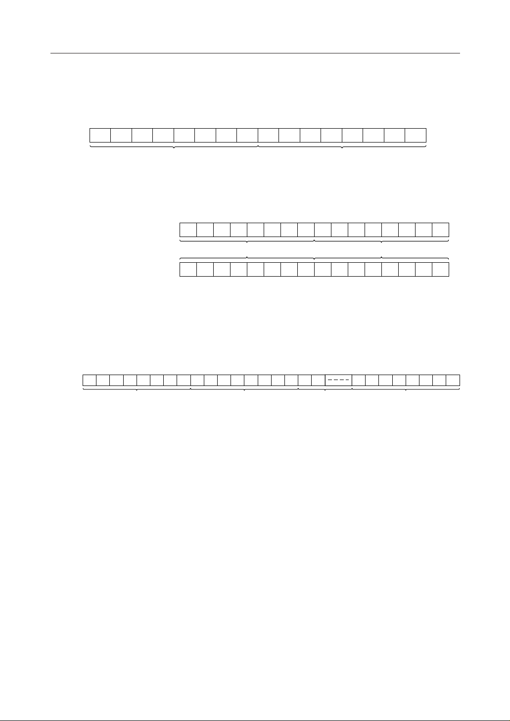
(3) Entry mode setting
PEDL9040A-03
ML9040A-Axx/-Bxx¡ Semiconductor
R/W
Instruction code LRSL
L
DB
DB
DB
DB
DB
DB
DB
I/D
DB
1
0
SH
7
6
5
4
3
2
L
L
L
L
H
1 When the I/D is set, the 8-bit character code is written or read to and from the DD
RAM, the cursor and blink shift to the right by 1 character position (I/D = "H";
increment) or to the left by 1 character position (I/D = "L"; decrement).
The address counter is incremented (I/D = "H") or decremented (I/D = "L") by 1 at
this time. Even after the character pattern code is written or read to and from the
CG RAM, the address counter (ADC) is incremented (I/D = "H") or decremented
(I/D = "L") by 1.
2 When SH = "H" is set, the character code is written to the DD RAM. Then the cursor
and blink stop and the entire display shifts to the left (I/D = "H") or to the right (I/
D = "L") by 1 character position.
When the character is read from the DD RAM during SH = "H", or when the
character pattern data is written or read to or from the CG RAM during SH = "H",
the entire display does not shift, but normal write/read is performed (the entire
display does not shift, but the cursor and blink shift to the right (I/D = "H") or to the
left (I/D = "L") by 1 character position.
When SH = "L" is set, the display does not shift, but normal write/read is performed.
The execution time when the OSC oscillation frequency is 270 kHz is 37 ms.
(4) Display mode setting
R/W
Instruction code LRSL
L
DB
DB
DB
DB
DB
DB
DB
7
6
5
4
3
2
L
L
L
H
DI
DB
1
0
C
B
1 The DI bit controls whether the character pattern is displayed or not displayed.
When DI is "H", this bit makes the LCD display the character pattern.
When DI is "L", the LCD character pattern is not displayed. The cursor and blink
are also cancelled at this time.
(Note) Unlike the display clear, the character code is not rewritten at all.
2 The cursor is not displayed when C = "L" and is displayed when DI = "H" and C =
"H".
3 The blink is cancelled when B = "L" and is executed when DI = "H" and B = "H".
In the blink mode, all dots (including the cursor) and displaying character pattern
and cursor are displayed alternately at 379.2 ms (in 5 x 7 dots character font) or 521.5
ms (in 5 x 10 dots character font) when the OSC oscillation frequency is 270 kHz. The
execution time when the OSC oscillation frequency is 270 kHz is 37 ms.
29/49
Page 30

(5) Cursor and display shift
PEDL9040A-03
ML9040A-Axx/-Bxx¡ Semiconductor
R/W
Instruction code LRSL
L
DB
DB
DB
DB
DB
DB
DB
7
6
5
4
3
2
L
L
H
D/C
R/L
DB
1
0
X
X
X : Don't Care
When D/C = "L" and R/L = "L", the cursor and blink positions are shifted to the left by
1 character position (ADC is decremented by 1).
When D/C = L and R/L = "H", the cursor and blink positions are shifted to the right by
1 character position (ADC is incremented by 1).
When D/C = "H" and R/L = "L", the entire display is shifted to the left by 1 character
position. The cursor and blink positions are also shifted with the display (ADC remains
unchanged).
When D/C = "H" and R/L = "H", the entire display is shifted to the right by 1 character
position. The cursor and blink positions are also shifted with the display (ADC remains
unchanged).
In the 2-line display mode, the cursor and blink positions are shifted from the first to
the second line when the cursor is shifted to the right next to the fortieth digit (27; hex.)
in the first line. No such shifting is made in other cases.
When shifting the entire display, the display pattern, cursor, and blink positions are in
no case shifted between lines (from the first to the second line or vice versa).
The execution time, when the OSC oscillation frequency is 270 kHz, is 37 ms.
(6) Initial setting
R/W
Instruction code LRSL
L
X : Don't Care
DB
DB
DB
DB
DB
DB
DB
7
6
5
4
3
2
L
H
8B/4B
N
F
DB
1
0
X
X
1 When 8B/4B = "H", the data input/output to and from the CPU is carried out
simultaneously by means of 8 bits DB7 to DB0.
When 8B/4B = "L", the data input/output to and from the CPU is carried out in two
steps through 4 bits of DB7 to DB4.
2 The 2-line display mode of the LCD is selected when N = "H", while the 1-line
display mode is selected when N = "L".
3 The 5 x 7 dots character font is selected when F = "L", while the 5 x 10 dots character
font is selected when F = "H" and N = "L".
This initial setting has to be accessed prior to other instructions except for the busy
flag read after the power is supplied to the ML9040A-Axx/-Bxx.
F
display lines
L
H
L
H
Number of
1 line 5 x 7 dots 1/8 84
1 line 5 x 10 dots 1/11 114
2 lines 5 x 7 dots 1/16 165
2 lines 1/16 1655 x 7 dots
N
L
L
H
H
Character
font
Duty
ratio
Number
of biases
Number of
COMMOM signals
30/49
Page 31
PEDL9040A-03
ML9040A-Axx/-Bxx¡ Semiconductor
Generate biases externally and input them to VDD, V1, V2, V3, V4, and V5.
When the number of biases is 4, input the same potential to V2 and V3. The execution
time, when the OSC oscillation frequency is 270 kHz, is 37 ms.
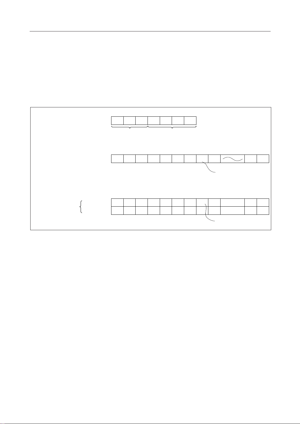
(7) CG RAM address setting
R/W
Instruction code LRSL
L
DB
DB
DB
DB
DB
DB
DB
7
6
5
4
3
2
H
C
C
C
5
4
C
3
2
DB
1
0
C
C
1
0
When CG RAM addresses, bits C5 to C0 (binary), are set, the CG RAM is specified, until
the DD RAM address is set.
Write/read of the character pattern to and from the CPU begins with addresses, bits C
to C0, starting from CG RAM selection.
The execution time, when the OSC oscillation frequency is 270 kHz, is 37 ms.
(8) DD RAM address setting
R/W
Instruction code LRSH
L
DB
DB
DB
DB
DB
DB
DB
7
6
5
4
3
2
D
D
D
D
6
5
4
D
3
2
DB
1
0
D
D
1
0
When the DD RAM addresses D6 to D0 (binary) are selected, the DD RAM is specified
until the DD RAM address is set.
Write/read of the character code to and from the CPU begins with addresses D6 to D
starting from DD RAM selection.
In the 1-line display mode (N = H), however, D6 to D0 (binary) must be set to one of the
values among "00" to "4F" (hex.).
Likewise, in the 2-line mode, D6 to D0 (binary) must be set to one of the values among
"00" to "27" (hex.) or "40" to "67" (hex.).
When any value other than the above is input, it is impossible to make a normal write/
read of character codes to and from the DD RAM.
The execution time, when the OSC oscillation frequency is 270 kHz, is 37 ms.
5
0
(9) DD RAM and CG RAM data write
R/W
Instruction code HRSE
L
DB
DB
DB
DB
DB
DB
DB
7
6
5
4
3
2
E
E
E
E
7
6
5
4
E
3
2
DB
1
0
E
E
1
0
When E7 to E0 (binary) codes are written to the DD RAM or CG RAM, the cursor and
display move as described in "(5) Cursor and display shift". The execution time, when
the OSC oscillation frequency is 270 kHz, is 37 ms.
31/49
Page 32

(10) Busy flag and address counter read (Execution time is 1 ms.)
PEDL9040A-03
ML9040A-Axx/-Bxx¡ Semiconductor
R/W
Instruction code LRSBF
H
DB
DB
DB
DB
DB
DB
DB
7
6
5
4
3
2
O
O
O
O
6
5
4
O
3
2
DB
1
0
O
O
1
0
The busy flag (BF) is output by this instruction to indicate whether the ML9040A-Axx/
-Bxx is engaged in internal operations (BF = "H") or not (BF = "L").
When BF = "H", no new instruction is accepted. It is therefore necessary to verify BF =
"L" before inputting a new instruction.
When BF = "L", a correct address counter value is output. The address counter value
must match the DD RAM address or CG RAM address. The decision of whether it is
a DD RAM address or CG RAM address is made by the address previously set.
Since the address counter value when BF = "H" is sometimes incremented or decremented
by 1 during internal operations, it is not always a correct value.
(11) DD RAM and CG RAM data read
R/W
Instruction code HRSP
H
DB
DB
DB
DB
DB
DB
DB
7
6
5
4
3
2
P
P
P
P
7
6
5
4
P
3
2
DB
1
0
P
P
1
0
Character codes (bits P7 to P0) are read from the DD RAM, while character patterns (P
to P0) from the CG RAM.
Selection of DD RAM or CG RAM is decided by the address previously set.
After reading those data, the address counter (ADC) is incremented or decremented by
1 as set by the shift mode mentioned in item "(3) shift mode set".
The execution time, when the OSC oscillation frequency is 270 kHz, is 37 ms.
7
(Note) Conditions for the reading of correct data:
1 When the DD RAM address set or CG RAM address set is input before
inputting this instruction.
2 When the cursor/display shift is input before inputting this instruction in
case the character code is read.
3 Data after the second reading from RAM when read more than 2 times.
Correct data is not output in any other case.
32/49
Page 33

PEDL9040A-03
ML9040A-Axx/-Bxx¡ Semiconductor
Interface with LCD and MSM5259
Display examples when setting the 5 x 7 dots character font 1-line mode, 5 x 10 dots character font
1-line mode, and 5 x 7 dots character font 2-line mode through instructions are shown in Figures
4, 5, and 6, respectively.
When the 5 x 7 dots character font is set in the 1-line display mode, the COM signals COM9 to
COM16 are output for extinguishing.
Likewise, when the 5 x 10 dots character font (1-line is set), the COM signals COM12 to COM
16
are output for display-off.
The display example shows a combination of 16 characters (32 characters for the 2-line display
mode) and the LCD. When the number of MSM5259s are increased according to the increase in
the number of characters, it is possible to display a maximum of 80 characters.
Besides, it is necessary to generate bias voltage required for LCD operation by splitting resistors
outside the IC to input it to ML9040A-Axx/-Bxx and MSM5259.
Examples of these bias voltages are shown in Figures 7, 8, 9, and 10. Basically, this can be done
by dividing the voltage by the resistors as shown in Figures 7 and 8. If the value of resistor R is
made larger to reduce system power consumption, the LCD operating margin decreases and the
LCD driving waveform is distorted. To prevent this, a by-pass capacitor is serially connected to
the resistor to lower voltage division impedance caused by the splitting of resistors as shown in
Figures 9 and 10.
As the values of R, VR, and C vary according to the LCD size used and V
(LCD drive voltage),
LCD
these values have to be determined through actual experimentation in combination with the
LCD.
(Example set values: R = 3.3 to 10kW, VR = 10 to 30kW, and C = 0.0022 mF to 0.047 mF)
Figure 17 shows an application circuit for the ML9040A-Axx/-Bxx and MSM5259 including a
bias circuit.
The bias voltage has to maintain the following potential relation:
VDD > V1 > V
≥ V
2
> V4 > V
3
5
• In the case of 1-line 16 characters display (5 x 7 dots/font)
COM
1
COM
8
SEG
1
ML9040A-Axx/-Bxx
DF L
SEG
40
DO
CP
DI
CP
Figure 4
LCD
O
1
1
MSM5259
DFLOAD DO
20DI21
O
40
33/49
Page 34

• In the case of 16-character (1 line) display (5 x 10 dots/font)
COM
1
COM
11
PEDL9040A-03
ML9040A-Axx/-Bxx¡ Semiconductor
LCD
SEG
1
ML9040A-Axx/-Bxx
DF L
SEG
40
DO
CP
O
1
DI
1
CP
Figure 5
• In the case of 16-character (2 lines) display (5 x 7 dots/font)
COM
1
COM
7
COM
8
COM
9
COM
15
COM
16
SEG
ML9040A-Axx/-Bxx
1
DF L
SEG
40
DO
CP
DI
1
CP
O
1
MSM5259
DFLOAD DO
MSM5259
DFLOAD DO
20DI21
20DI21
O
40
LCD
O
40
Figure 6
34/49
Page 35

PEDL9040A-03
ML9040A-Axx/-Bxx¡ Semiconductor
• Bias voltage circuit (1-line display mode) • Bias voltage circuit (2-line display mode)
V
ML9040A-Axx/-Bxx
DD
R
V
1
V
2
V
3
V
4
R
V
R
LCD
ML9040A-Axx/-Bxx
R
V
5
VR
V
DD
R
V
1
R
V
2
R
V
3
V
LCD
R
V
4
VR
V
5
Figure 7
Figure 8
• Bias voltage circuit (1-line display mode) • Bias voltage circuit (2-line display mode)
V
DD
V
1
V
2
V
3
V
4
V
5
Figure 10
R
C
R
C
R
R
V
C
C
RC
LCD
VR
C
ML9040A-Axx/-Bxx
(V
: LCD driving voltage)
LCD
V
DD
V
V
V
V
V
1
2
3
4
5
Figure 9
R
R
R
R
C
C
V
LCD
ML9040A-Axx/-Bxx
C
C
VR
C
35/49
Page 36

• Application circuit
LCD
40
- O
1
O
MSM5259
40
- O
1
O
MSM5259
40
- O
1
O
MSM5259
40DO20
DO
1
DI
40DO20
DO
DI1CP
40DO20
DO
DI1CP
PEDL9040A-03
ML9040A-Axx/-Bxx¡ Semiconductor
21
EE
V
DI
3
V
2
V
SS
V
LOAD
21
DI
LOAD
21
DI
LOAD
DD
DF
V
EE
V
3
V
2
V
SS
V
DD
DF
V
C
C
EE
V
3
V
2
V
SS
V
DD
DF
V
C
C
C
C
0V
VR
R
R
R
R
R
+5V
CP
40
-
1
SEG
16
-
1
COM
DO
CP
Figure 11
L
DF
VDDGND
ML9040A-Axx/-Bxx
1V2V3
V
4V5
V
36/49
Page 37

PEDL9040A-03
ML9040A-Axx/-Bxx¡ Semiconductor
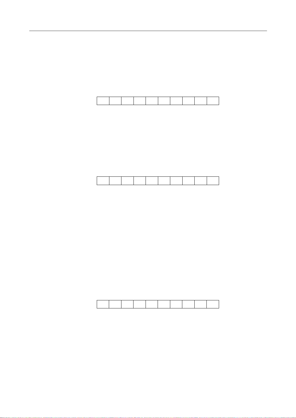
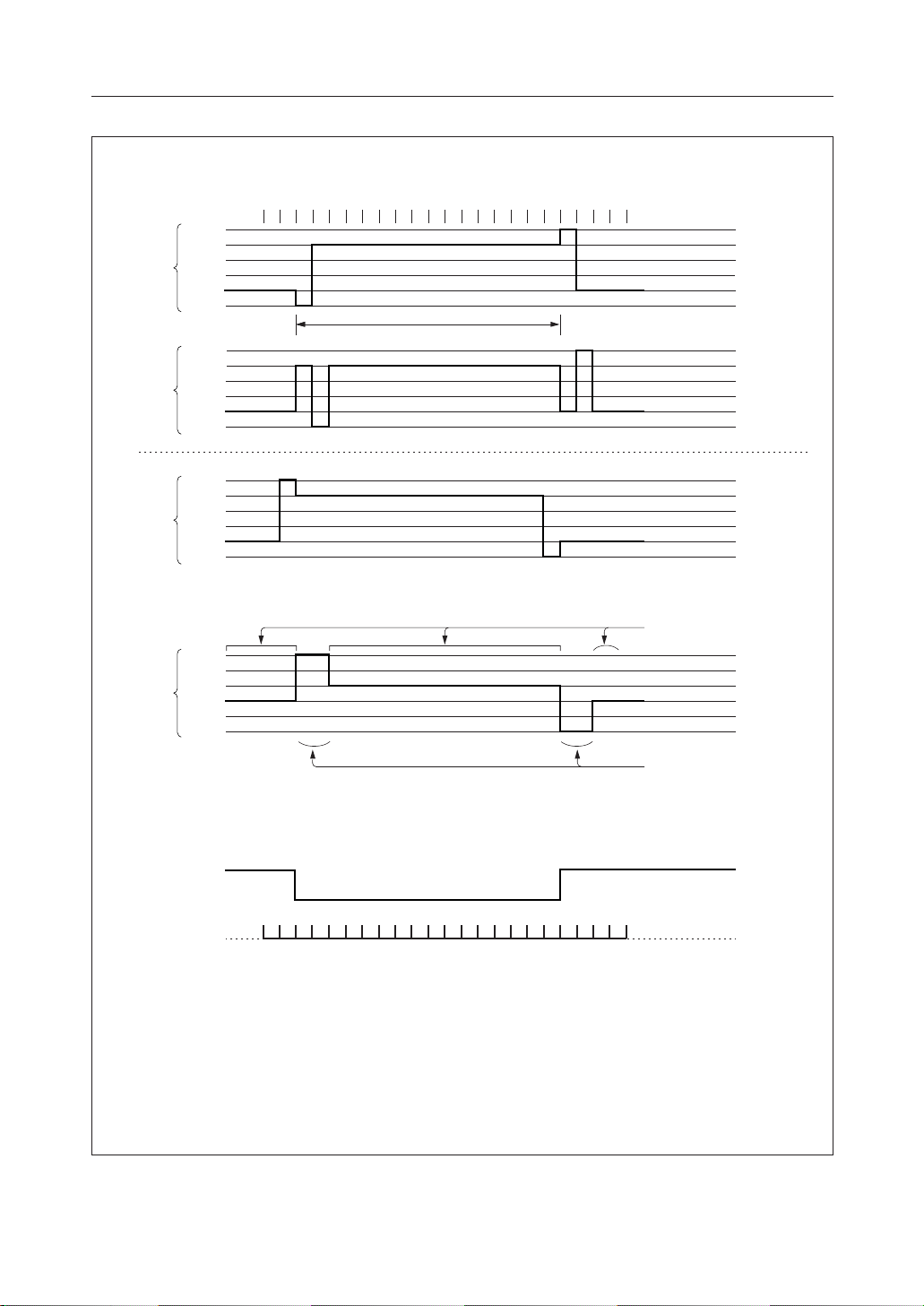
LCD Drive Waveforms
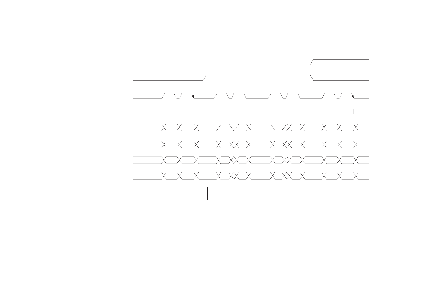
Figures 12, 13 and 17 show the LCD driving waveforms consisting of COM signal, SEG signal,
DF signal and L (latch pulse waveform) signal, in the duty of 1/8, 1/11 and 1/16 respectively.
The relation between duty and frame frequency is described in the table below.
Duty
1/8 84.3 Hz
1/11 61.4 Hz
1/16 84.3 Hz
Frame frequency
(Note) The OSC oscillation frequency is assumed to be 270 kHz.
37/49
Page 38
PEDL9040A-03
ML9040A-Axx/-Bxx¡ Semiconductor
COM
COM
COM
COM
COM
V
DD
V
V
1
1
V
2,V3
V
V
4
V
V
5
V
DD
V
V
1
2
V2,V
V
V
4
V
V
5
V
DD
V
V
1
8
V2,V
V
V
4
V
V
5
V
DD
V
V
1
9
V2,V
V
V
4
V
V
5
V
DD
V
V
1
16
V2,V
V
V
4
V
V
5
81234567812
1 frame
3
3
3
3
SEG
(Output
example)
V
DD
V
V
1
V2,V
V
V
4
V
V
5
DF
L
Display-off
waveform
3
Display-on
waveform
Figure 12. LCD Driving Waveforms (A mode) at 1/8 Duty
38/49
Page 39

PEDL9040A-03
ML9040A-Axx/-Bxx¡ Semiconductor
COM
COM
COM
COM
COM
V
DD
V
V
1
V2,V
V
V
V
V
V
V
V
2
V
V
V
V
V
V
DD
V
V
11
V2,V
V
V
V
V
V
DD
V
V
12
V2,V
V
V
V
V
V
DD
V
V
16
V2,V
V
V
V
V
11123456789101112
1
3
4
5
DD
1
2,V3
4
5
1
4
5
1
4
5
1
4
5
3
3
3
1 frame
SEG
(Output
example)
V
DD
V
V
1
V2,V
3
V
V
4
V
V
5
DF
L
Figure 13. LCD Driving Waveforms (A mode) at 1/11 Duty
Display-off
waveform
Display-on
waveform
39/49
Page 40

PEDL9040A-03
ML9040A-Axx/-Bxx¡ Semiconductor
COM
COM
COM
SEG
(Output
example)
V
V
V
1
V
V
V
V
V
V
V
V
V
V
2
V
V
V
V
V
V
V
V
16
V
V
V
1612 3456 7891011
DD
1
2
3
4
5
DD
1
2
3
4
5
DD
1
2
3
4
5
1 frame
13 14 15 16 1 212
Display-off
waveform
V
DD
V
V
1
V
V
2
V
3
V
4
V
5
Display-on
waveform
DF
L
Figure 14. LCD Driving Waveforms (A mode) at 1/16 Duty
40/49
Page 41

PEDL9040A-03
ML9040A-Axx/-Bxx¡ Semiconductor
COM
COM
COM
COM
COM
V
DD
V
V
1
1
V2,V
3
V
V
4
V
V
5
V
DD
V
V
1
2
V2,V
3
V
V
4
V
V
5
V
DD
V
V
1
8
V2,V
3
V
V
4
V
V
5
V
DD
V
V
1
9
V2,V
3
V
V
4
V
V
5
V
DD
V
V
1
16
V2,V
3
V
V
4
V
V
5
7 8 1 2 3 4 5 6 7 8 1 2 3 4 5 6 7 8 1 2
1 frame
SEG
(Output
example)
Display turning-off
V
DD
V
V
1
V2,V
V
V
4
V
V
5
3
waveform
Display turning-on
waveform
DF
L
Figure 15. LCD Driving Waveforms (B mode) at 1/8 Duty
41/49
Page 42

PEDL9040A-03
ML9040A-Axx/-Bxx¡ Semiconductor
COM
COM
COM
COM
COM
V
DD
V
V
1
1
V2,V
3
V
V
4
V
V
5
V
DD
V
V
1
2
V2,V
3
V
V
4
V
V
5
V
DD
V
V
1
11
V2,V
3
V
V
4
V
V
5
V
DD
V
V
1
12
V2,V
3
V
V
4
V
V
5
V
DD
V
V
1
16
V2,V
3
V
V
4
V
V
5
1011 1 2 3 4 5 6 7 8 9 1011 1 2 3 4 5
1 frame
SEG
(Output
example)
Display turning-off
V
DD
V
V
1
V2,V
V
V
4
V
V
5
3
waveform
Display turning-on
waveform
DF
L
Figure 16. LCD Driving Waveforms (B mode) at 1/11 Duty
42/49
Page 43
PEDL9040A-03
ML9040A-Axx/-Bxx¡ Semiconductor
COM
COM
COM
SEG
(Output
example)
V
DD
V
V
1
1
V
V
2
V
3
V
4
V
5
V
DD
V
V
1
V
V
2
2
V
3
V
4
V
5
V
DD
V
V
1
V
V
2
16
V
3
V
4
V
5
15 16 1 2 3 4 5 6 7 8 9 10 11 12 13 14 15 16 1 2 3 4
1 frame
Display turning-off
V
DD
V
V
1
V
V
2
V
3
V
4
V
5
waveform
Display turning-on
waveform
DF
L
Figure 17. LCD Driving Waveforms (B mode) at 1/16 Duty
43/49
Page 44

PEDL9040A-03
ML9040A-Axx/-Bxx¡ Semiconductor
Initial Setting of Instruction
(1) When data input/output to and from the CPU is carried out by 8 bits (DB0 to DB7):
q Turn on the power.
w Wait for 15 ms or more after VDD has reached 4.5V or more.
e Set 8B by initial setting of instruction.
r Wait for 4.1 ms or more.
t Set 8B by initial setting of instruction.
y Wait for 100 ms or more.
u Set 8B by initial setting of instruction.
i Check the busy flag as No Busy.
o Set 8B. Set LCD line number (N) and character font (F).
(After this, the LCD line number and character font cannot be changed.)
!0 Check No Busy.
!1 Clear the display by setting the display mode.
!2 Check No Busy.
!3 Clear the display.
!4 Check No Busy.
!5 Set the shift mode.
!6 Check No Busy.
!7 Initial setting completed.
Example of Instruction Code for Steps e, t, and u.
R/WLRSLDB
L
X : Don't Care
DB
DB
DB
DB
DB
DB
7
6
5
4
3
2
L
H
H
X
X
DB
1
0
X
X
44/49
Page 45

PEDL9040A-03
ML9040A-Axx/-Bxx¡ Semiconductor
(2) When data input/output to and from the CPU is carried out by 4 bits (DB4 to DB7):
q Turn on the power.
w Wait for 15 ms or more after VDD has reached 4.5V or more.
e Set 8B by initial setting of instruction.
r Wait for 4.1 ms or more.
t Set 8B by initial setting of instruction.
y Wait for 100 ms or more.
u Set 8B by initial setting of instruction.
i Check the busy flag as No Busy.
o Set 4B by initial setting of instruction.
!0 Wait for 100 ms or more.
!1 Set 4B, LCD line number (N) and character font (F) by initial setting of instruction.
(After this, the LCD line number and character font cannot be changed.)
!2 Check No Busy.
!3 Clear the display by setting the display mode.
!4 Check No Busy.
!5 Clear the display.
!6 Check No Busy.
!7 Set the shift mode.
!8 Check No Busy.
!9 Initialization completed.
Example of Instruction Code for Steps e, t, and u.
R/WLRSLDB
L
DB
DB
7
6
L
DB
5
4
H
H
Example of Instruction Code for Step o.
R/WLRSLDB
L
DB
DB
7
6
L
DB
5
4
H
L
Example of Instruction Code for Step i.
RS
RS
0
L
R/WBFDB
H
1
H
DB
DB
7
6
Q
6
DB
5
4
Q
Q
5
4
Execute two-step accesses in 4 bits from Step !1 to Step !8.
45/49
Page 46

PAD CONFIGURATION
Pad Layout
Chip size: 2.94 x 4.32 mm
Passivation film etched hole: 80 x 80 mm
57
PEDL9040A-03
ML9040A-Axx/-Bxx¡ Semiconductor
Y
43
58
81
17
SEG19
SEG18
SEG17
SEG16
SEG15
SEG14
SEG13
SEG12
SEG11
SEG10
SEG9
SEG8
SEG7
SEG6
SEG5
SEG4
SEG3
SEG2
SEG1
TEST
SEG38
SEG37
SEG36
SEG35
SEG34
SEG33
SEG32
SEG31
SEG30
SEG29
SEG28
SEG27
SEG26
SEG25
SEG24
SEG23
SEG22
SEG21
SEG20
1
–1310
–1156
–1002
–848
–694
–540
–386
–233
–79
75
229
383
537
691
845
999
1153
1309
1311
1311
Y (µm)X(µm)
–1955
–1955
–1955
–1955
–1955
–1955
–1955
–1955
–1955
–1955
–1955
–1955
–1955
–1955
–1955
–1955
–1955
–1955
–1615
–1478
Pad Pad Name
21
Pad Coordinates
Pad Pad Name
1 SEG39
222
323
424
525
626
727
828
929
10 30
11 31
12 32
13 33
14 34
15 35
16 36
17 37
18 38
19 39
20 40
42
18
X
1311
1311
1311
1311
1311
1311
1311
1311
1311
1311
1311
1311
1311
1311
1311
1311
1311
1311
1311
1311
Y (µm)X(µm)
–1342
–1206
–1070
–934
–797
–661
–525
–389
–253
–116
156
292
428
565
701
837
973
1109
1296
20
46/49
Page 47

PEDL9040A-03
ML9040A-Axx/-Bxx¡ Semiconductor
Pad Pad Name
41 GND
42
43
44
45
46
47
48
49
50
51
52
53
54
55
56
57
58
59
60
61
62
63
64
65
66
67
68
69
70
71
72
73
74
75
76
77
78
79
80
81
OSC1
OSC2
V1
V2
V3
V4
V5
L
CP
V
DD
DF
DO
RS
RW
E
DB0
DB1
DB2
DB3
DB4
DB5
DB6
DB7
COM1
COM2
COM3
COM4
COM5
COM6
COM7
COM8
COM9
COM10
COM11
COM12
COM13
COM14
COM15
COM16
SEG40
1311
1311
1049
738
576
414
252
90
—347
—491
—610
—710
—810
—910
—1010
—1111
—1211
—1311
—1311
—1311
—1311
—1311
—1311
—1311
—1311
—1311
—1311
—1311
—1311
—1311
—1311
—1311
—1311
—1311
—1311
—1311
—1311
—1311
—1311
—1311
—1311
Y(mm)X(mm)
1426
1955
1955
1955
1955
1955
1955
1955
1955
1955
1955
1955
1955
1955
1955
1955
1955
1955
1783
1369
1184
1000
816
632
148
48
—52
—152
—253
—353
—453
—553
—653
—754
—854
—954
—1054
—1154
—1255
—1355
—1455
47/49
Page 48

PACKAGE DIMENSIONS
QFP80-P-1420-0.80-BK
Mirror finish
PEDL9040A-03
ML9040A-Axx/-Bxx¡ Semiconductor
(Unit : mm)
Package material
Lead frame material
Pin treatment
Package weight (g)Oki Electric Industry Co., Ltd.
Rev. No./Last Revised
Epoxy resin
42 alloy
Solder plating (≥5 mm)
1.27 TYP.
4/Nov. 28, 1996
Notes for Mounting the Surface Mount Type Package
The SOP, QFP, TSOP, TQFP, LQFP, SOJ, QFJ (PLCC), SHP, and BGA are surface mount type
packages, which are very susceptible to heat in reflow mounting and humidity absorbed in
storage. Therefore, before you perform reflow mounting, contact Oki’s responsible sales person
on the product name, package name, pin number, package code and desired mounting conditions
(reflow method, temperature and times).
48/49
Page 49

PEDL9040A-03
ML9040A-Axx/-Bxx¡ Semiconductor
NOTICE
1. The information contained herein can change without notice owing to product and/or
technical improvements. Before using the product, please make sure that the information
being referred to is up-to-date.
2. The outline of action and examples for application circuits described herein have been
chosen as an explanation for the standard action and performance of the product. When
planning to use the product, please ensure that the external conditions are reflected in the
actual circuit, assembly, and program designs.
3. When designing your product, please use our product below the specified maximum
ratings and within the specified operating ranges including, but not limited to, operating
voltage, power dissipation, and operating temperature.
4. Oki assumes no responsibility or liability whatsoever for any failure or unusual or
unexpected operation resulting from misuse, neglect, improper installation, repair, alteration
or accident, improper handling, or unusual physical or electrical stress including, but not
limited to, exposure to parameters beyond the specified maximum ratings or operation
outside the specified operating range.
5. Neither indemnity against nor license of a third party’s industrial and intellectual property
right, etc. is granted by us in connection with the use of the product and/or the information
and drawings contained herein. No responsibility is assumed by us for any infringement
of a third party’s right which may result from the use thereof.
6. The products listed in this document are intended for use in general electronics equipment
for commercial applications (e.g., office automation, communication equipment,
measurement equipment, consumer electronics, etc.). These products are not authorized
for use in any system or application that requires special or enhanced quality and reliability
characteristics nor in any system or application where the failure of such system or
application may result in the loss or damage of property, or death or injury to humans.
Such applications include, but are not limited to, traffic and automotive equipment, safety
devices, aerospace equipment, nuclear power control, medical equipment, and life-support
systems.
7. Certain products in this document may need government approval before they can be
exported to particular countries. The purchaser assumes the responsibility of determining
the legality of export of these products and will take appropriate and necessary steps at their
own expense for these.
8. No part of the contents contained herein may be reprinted or reproduced without our prior
permission.
9. MS-DOS is a registered trademark of Microsoft Corporation.
Copyright 2000 Oki Electric Industry Co., Ltd.
Printed in Japan
49/49
 Loading...