
D
ATA
S
HEET
10-Gbps GaAs Family
High-Speed Optical Communications System
April 1999
O K I
G a A s
P R O D U C T S

■ ■
–––––––––––––––––––––––––––––––––––––––––––––––––––––––––––––––––––––––––––––––––––––––––––
Oki Semiconductor
CONTENTS
10-GHz GaAs Family
.........................................................................................................................1
KGL4201
10-GHz 8:1 Multiplexer ............................................................................................................................. 3
KGL4202
10-GHz 1:8 Demultiplexer ........................................................................................................................ 7
GHDD4411
EX-OR Circuit.......................................................................................................................................... 11
GHDD4414
Decision Circuit with Phase Detector...................................................................................................... 15
1Oki Semiconductor
10-GHz GaAs Family
High-Speed Optical Communications Systems
INTRODUCTION
Oki’s 10-GHz logic devices are manufactured using a 0.2-µm, ion-implanted process, which is similar to
Oki’s familiar 0.5-µm telecommunications process. However, the 0.2-µm process uses a phase-shifting
edge line (PEL) masking method for gate fabrication. Gold-based, three-level metal interconnections are
used for high density and shorter wiring paths. Layers 1 and 2 are signal lines. Layer 3, which is formed
by electroplating, is used for ground or power supply lines because of its lower resistance. An optional
buried “p” channel structure is adopted for reducing short channel effects.
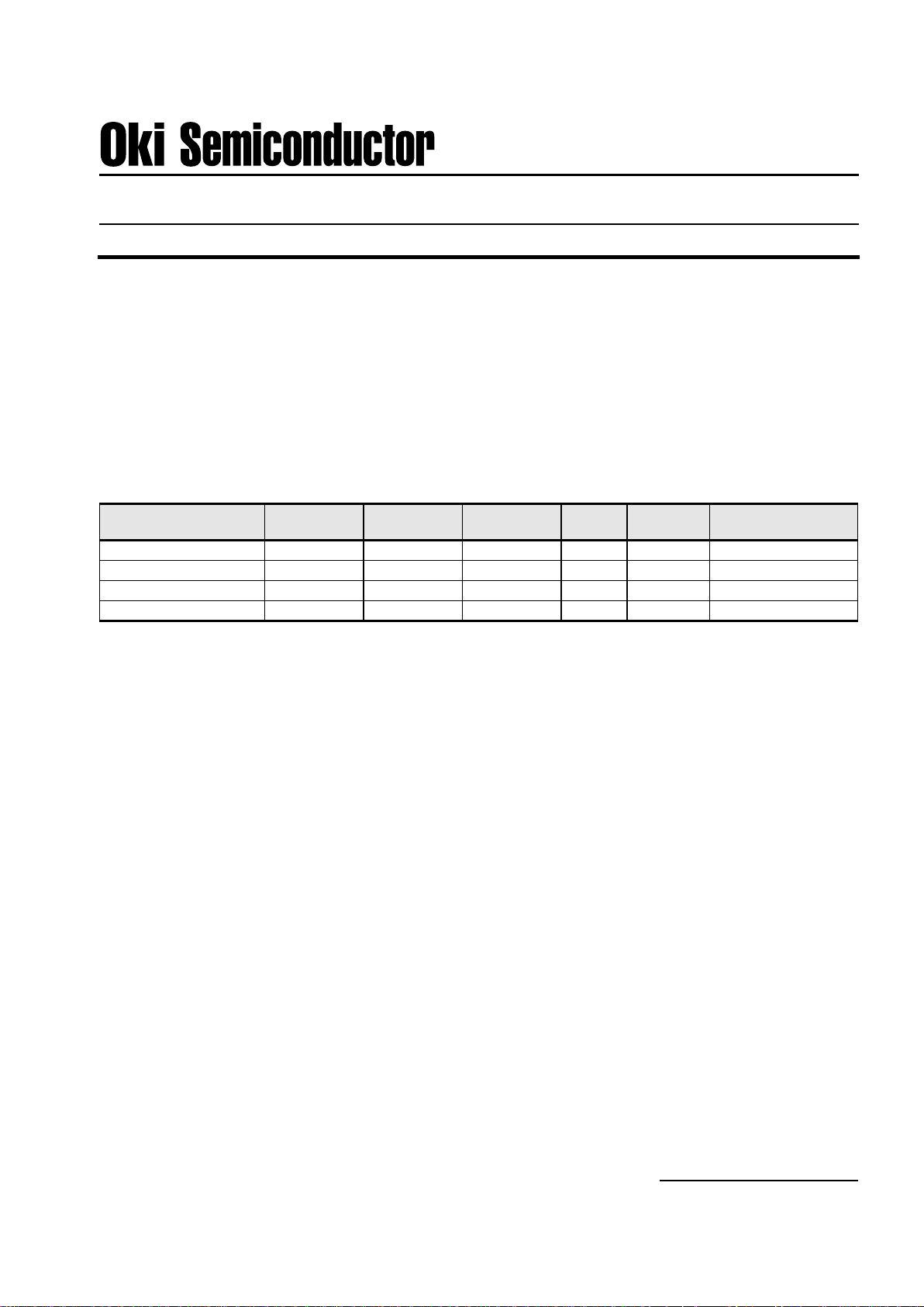
The following table shows the digital GaAs logic processes of the 10-GHz GaAs family.
The key to operating reliably at 10 Gbps is logic circuitry that can easily manipulate data at over 13 Gbps.
The higher frequency overhead is required to meet the different clock skews encountered when designing and routing 10-Gbps data management hardware.
The logic is either direct-coupled FET logic (DCFL) or source-coupled FET logic (SCFL). The low-drive
disadvantage of DCFL can be improved by using super-buffer FET logic (SBFL). The basic speed of SBFL
is slower than DCFL, but SBFL is faster with higher fanouts and longer metal runs. A designer selects the
best performing logic for each logic element application. SBFLs used for clock distribution, output buffers, etc. Typical gate delays of 9 ps and power of 2 mW per gate are achieved. Register logic elements like
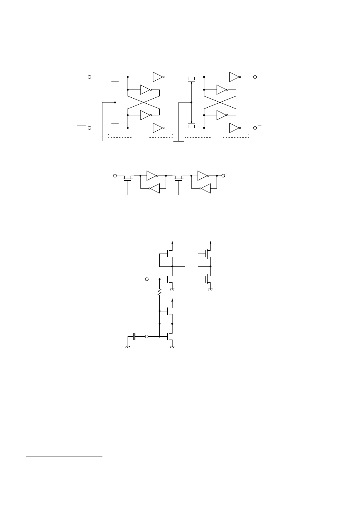
D-flip flops are assembled using memory cell flip flops (MCFF) as shown in Figure 1 .The operation speed
of a MCFF, which is about twice that of a conventional 6 NOR-gate circuit, operates at very low power.
To simplify device interconnections, AC-coupled clock and data input lines are created using the circuit
shown in Figure 2 .
FEATURES
GaAs Logic Processes
Basic FET Process
Basic Gate
Circuit
Photo Masking
Gate Length
(µm)
fT (GHz)
Gate Delays
(ps)
Application
MESFET DCFL or SBFL I-line printing 0.5 30 25 < 2.4 Gbps standard cell
MESFET DCFL or SBFL PEL < 0.2 60 9 >12-Gbps hand-routed logic
Pseudomorphic-inverted HEMT DCFL or SBFL PEL 0.2 > 60 7 > 20-Gbps low-density logic
Pseudomorphic BP--MESFET Analog Deep UV 0.2 > 60 – Analog amplifier
• 10-Gbps operation: highest speed available
• ECL level logic swings: easy interface to other
logic
• Inputs internally terminated: reduces noise and
phase jitter
• 50-Ω I/Os: easy to interconnect hardware
■
10-GHz GaAs Family ■ ––––––––––––––––––––––––––––––––––––––––––––––––––––––––––––––––––––––––––
2 Oki Semiconductor
Many 10-Gbps inputs are self-biased and 50-
Ω
terminated, for capacitance coupling. The outputs are DC-
coupled to drive 50-
Ω
ground terminated lines.
DATA SHEETS
This document contains data sheets for the KGL4201, KGL4202, GHDD4411, and GHDD4414 10-Gbps
GaAs High-Speed Optical Communication Systems.
Data sheets for other communication devices may be obtained from the Oki Semiconductor WEB site,
www.okisemi.com or from the local sales office.
Figure 1. Memory Cell Flip-Flops
Data
Data
Clock Clock
Q
Q
Master Slave
Master/Slave Flip-Flop
Data
Clock Clock
Out
Flip-Flop
Figure 2. AC-Coupled, Self-Biased Logic Input
Data or Clock In
50Ω
Reference
Dummy Gate
3Oki Semiconductor
KGL4201
10-GHz 8:1 Multiplexer
GENERAL DESCRIPTION
Oki’s KGL4201 is a 10-GHz 8:1 multiplexer designed to operate in 10-Gbps communication links. This
circuit synchronously merges eight 1.25-Gbps data streams, clocked at low frequency rates into a single
10-Gbps stream, clocked at the higher frequency. In the KGL4201 multiplexer, the 10-GHz master clock is
first divided by two, then by four. The lower frequency components are first multiplexed by four, then
the two groups are merged into a single data stream using the master 10-Gbps clock. Complementary
1/8 synchronous clock outputs are made available from the KGL4201 for use in synchronizing lower frequency logic.
All signal interfaces are 50-
Ω
with direct DC coupling on the 1.25-Gbps data inputs and phase-locked
1.25-Gbps clock outputs. The 10-Gbps data output and 10-GHz clock input are AC-capacitively-coupled
for ease of interfacing at microwave speeds and reducing ground noise induced phase jitter. All package
clock and data pins are separated by either ground or supply voltage pins to control the I/O impedance,
maintain signal isolation and reduce phase noise.
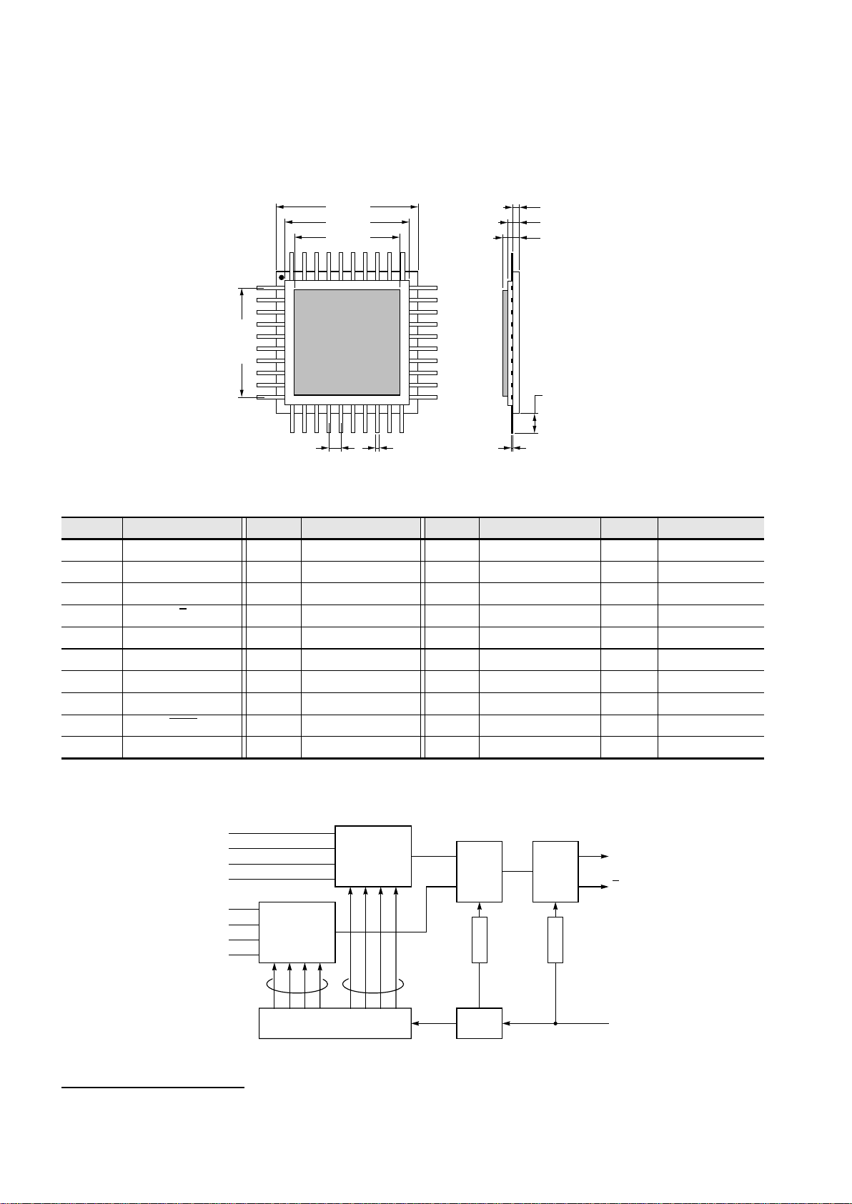
The KGL4201 is shipped in a 40-pin ceramic flat-package with impedance-controlling ground plane and
flush mounting bottom heat sink.
FEATURES
• AC-coupled 10 Gbps I/O: eliminates DC
coupled phase jitter
• 1/8 clock generated on chip: easy to
synchronize downstream logic
• 2 V, 2.4 W
• Isolated I/O pins: minimize noise and
impedance variation
• Packaged in 40-pin ceramic flat-package with
ground plane and heat sink.
■
KGL4201 ■ –––––––––––––––––––––––––––––––––––––––––––––––––––––––––––––––––––––––––––––––––––
4 Oki Semiconductor
1
10
20
31
11
21
30
40
11.0 SQ
13.01 SQ
14.84 SQ
1.27
2 ±0.3
0.4 ±0.05
1.7 ±0.15
0.7 ±0.05
0.9 ±.005
PIN CONFIGURATION
BLOCK DIAGRAM
Pin Configuration
Pin
Name Pin Pin Name Pin Pin Name Pin Pin Name
1 GND 11 GND 21 VDD 31 GND
2 Q 12 VDD 22 GND 32 VDD
3 GND 13 D0 23 GND 33 D7
4Q
14 GND 24 CK 34 GND
5 GND 15 D2 25 GND 35 D5
6 GND 16 D4 26 GND 36 D3
7 1/8CK 17 GND 27 RCK 37 GND
8 GND 18 D6 28 GND 38 D1
9 1/8CK
19 GND 29 GND 39 VB
10 VB 20 GND 30 GND 40 VDD
1
10
20
31
11
21
30
40
10.67 SQ
11.43 SQ
13.01 SQ
14.84 SQ
1.27
2 ±0.3
0.125 ±0.050.4 ±0.05
1.7 ±0.15
0.7 ±0.05
0.9 ±.005
D0
D2
D4
D6
D1
D3
D5
D7
4:1 MUX
1/8CK 1/8CK
4:1 MUX
2:1
MUX
Output
Latch
Q
Q
delay
delay
1/2
Divider
1/4 Divider CK
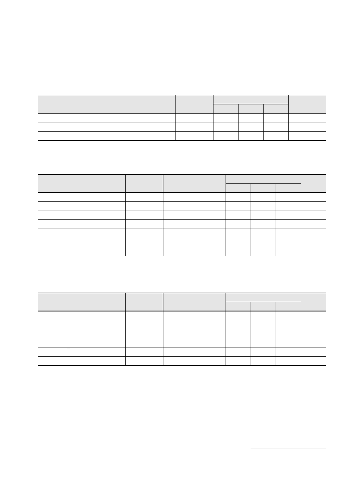
––––––––––––––––––––––––––––––––––––––––––––––––––––––––––––––––––––––––––––––––––– ■ KGL4201 ■
5Oki Semiconductor
ELECTRICAL CHARACTERISTICS
RECOMMENDED OPERATING CONDITIONS
Parameter
Symbol
Rated Value
UnitMin Typ Max
Power supply voltage for internal logic V
DD
1.9 2.0 2.1 V
Power supply voltage for output buffer V
B
1.9 2.0 2.1 V
Operating temperature range at package base T
S
0 – 70 °C
DC CHARACTERISTICS
V
DD
= 2V ±0.1V, VB=2V ±0.1V Ts = 0 to 70°C
Parameter Symbol Test Condition
Rated Value
UnitMin. Typ. Max.
Power dissipation P – 2.4 3.0 W
High-level 1/8 CK output voltage V
OH
0.85 1.3 V
Low-level 1/8 CK output voltage V
OL
0 0.3 V
Data output voltage swing V
OD
50-
Ω
load 0.7 1.2 V
P-P
Clock input voltage swing V
CK
Capacitive coupling 0.5 0.9 V
P-P
High-level data input voltage V
IDH
0.8 1.3 V
Low-level data input voltage V
IDL
0 0.3 V
AC CHARACTERISTICS
VDD = 2V ±0.1V, VB=2V ±0.1V Ts = 0 to 70°C
Parameter Symbol Test Condition
Rated Value
UnitMin. Typ. Max.
Minimum clock period
∆
t
C
– – 100 ps
Setup time (Data to 1/8 CK ↓)t
PS
450 500 550 ps
Hold time (1/8 CK ↓ to Data) t
DH
-400 -350 -300 ps
CK-D[7:0] phase margin
∆
t
M
Input clock period is 100 ps 550 650 ps
Rise time (Q, Q
)t
R
20 30 40 ps
Fall time (Q, Q
)t
F
20 30 40 ps
■ KGL4201 ■ –––––––––––––––––––––––––––––––––––––––––––––––––––––––––––––––––––––––––––––––––––
6 Oki Semiconductor
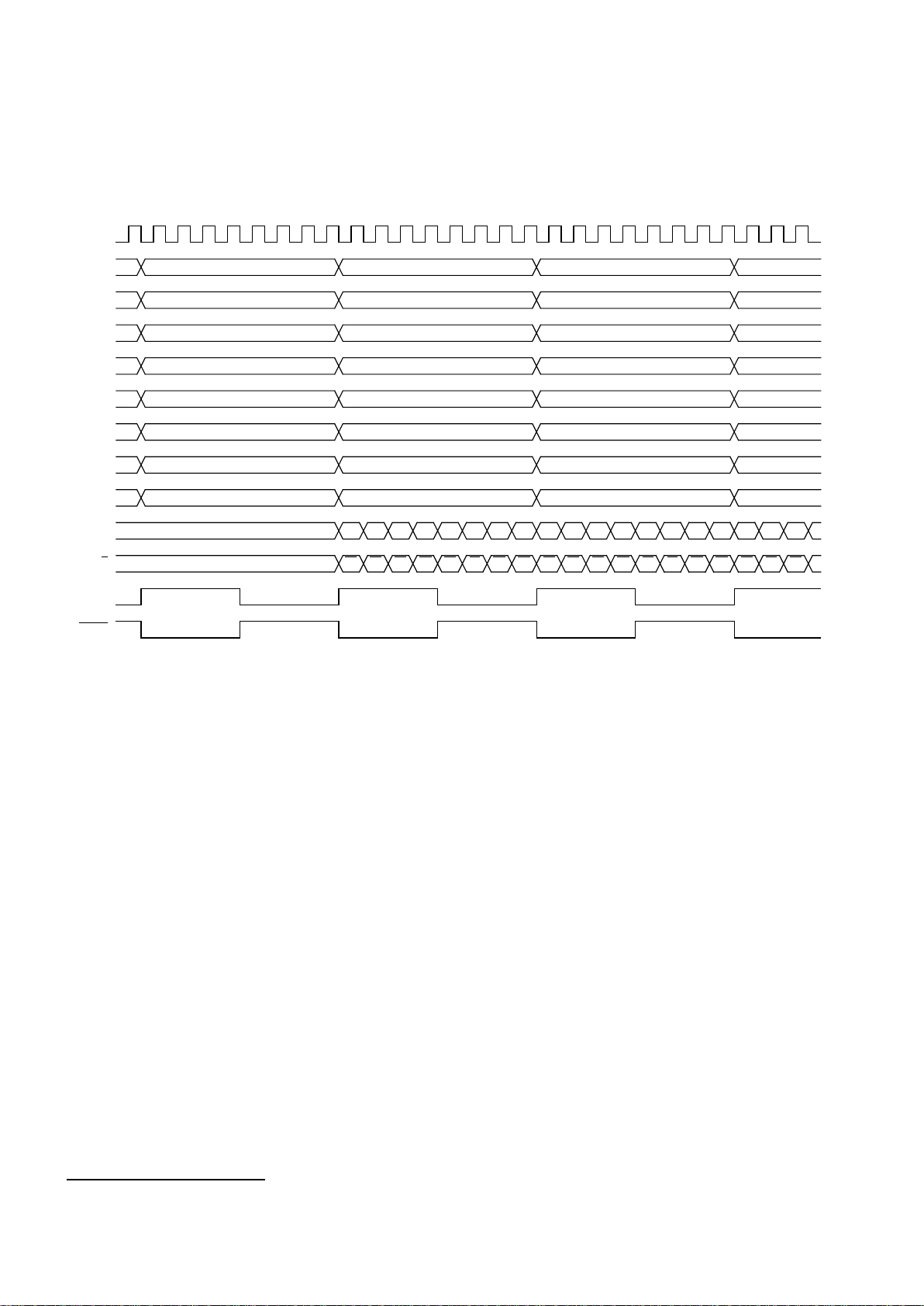
INTERFACE TIMING
CK
D0
D1
D2
D3
D4
D5
D6
D7
Q
A1 A2 A3 A4
B1 B2 B3 B4
C1 C2 C3 C4
D1 D2 D3 D4
E1 E2 E3 E4
F1 F2 F3 F4
G1 G2 G3 G4
H1 H2 H3 H4
H1G1F1E1D1C1B1A1 H2G2F2E2D2C2B2A2 C3B3A3
Q H1 G1 F1 E1 D1 C1 B1 A1 H2 G2 F2 E2 D2 C2 B2 A2 C3 B3 A3
1/8 CK
1/8 CK
 Loading...