

Page 1
OKIPAGE4w
LED Page Printer
Troubleshooting Manual
with Component Parts List
(ODA/OEL/INT)
APPROVAL
All specifications are subject to change without notice.
Page 2

Page 3

CONTENTS
1. OUTLINE..................................................................................................... 1
2. TOOLS........................................................................................................ 1
3. CIRCUIT DESCRIPTION............................................................................ 2
4. TROUBLESHOOTING.............................................................................. 21
5. CIRCUIT DIAGRAM.................................................................................. 27
6. COMPONENT PARTS LIST
Page 4
1. OUTLINE
This manual has been written to provide guidance for troubleshooting of the OKIPAGE4w Plus
Printer (primarily for its printed circuit boards), on an assumption that the reader is knowledgeable
of the printer. Read the maintenance manual for this printer P/N M-521426 if necessary.
Note:
1. High voltage power supply board and power supply unit containing a high voltage power
supply is dangerous. From the viewpoint of the safety standards, the local repairing of a
defective board is not allowed. Thus, the objects to be locally repaired as a result of
troubleshooting are switches and fuses.
2. TOOLS
For troubleshooting the printer, the tools listed below may be needed in addition to general
maintenance tools.
Oscilloscope Frequency response 100 MHz or higher
Soldering iron A slender tip type, 15-20 watts
Extension code kit P/N : 40105501
Tool Remarks
- 1 -
Page 5

3. CIRCUIT DESCRIPTION
3.1 Outline
The circuit of OKIPAGE4w Plus consists of a main control board, a high voltage power supply
board and a power supply unit. The block diagram is shown in Fig. 3-1. The main control board
controls the reception and transmission of data with a host I/f and processes command analysis,
bit image development, raster buffer read. It also controls the engine and high voltage outputs.
(1) Reception and transmission control
The main control board has one parallel I/F port which is compliant to the IEEE 1284
specification.
An interface task stores all data received from the host into a receive buffer first, and returns
the printer status upon request of the host.
(2) Command analysis processing
The OKIPAGE4w Plus printer has the following emulation mode.
Hiper-W: OKI original
An edit task fetches data from the receive buffer, analizes commands, and sets I/O registers.
(3) Raster data processing
The decompression circuit in the CPU expands the compressed data and stores the data into
the raster buffer.
(4) Raster data transfer
The LED head control circuit in the CPU sends the data stored in the raster buffer to the LED
head.
(5) High voltage control
The high voltage control circuit in the CPU.
The high voltage power supply board generates high voltage outputs, and have sensors, LED for
display.
The power supply unit generates +24VDC output, +5DC output.
- 2 -
Page 6
10MHz
CPU
(MSM65917)
EEPROM
Parallel
Figure 3-1 OKIPAGE4w Plus Block Diagram
I/F
A8 ~ A15
AD0 ~ AD7
Address
latch
A0 ~ A7
EPROM
(64 KByte)
D0 ~ D7
CN
Parallel
I/F
LS07
LED head LED head
Parallel
I/F
- 3 -
LED head
Main motor
Electromagnetic
5V
clutch
Sensors
TEMP
TR-VSEN
TR-ISEN
Reset
circuit
5V
0VL
A0 ~ A9
Driver
D0 ~ D3
D-RAM
128 KByte
or
512 KByte
High-voltage power I/F
LED
HEAT ON
<Main Control Board>
HEAT ON
Main motor
Electromagnetic
clutch
LED
Sensors
TEMP
High-voltage
power
TR-VSEN
TR-ISEN
Driver
+24V
+5V
0VL
0VP
Driver
Driver
Manual feed sensor
LED
Paper sensor
Outlet sensor
Toner sensor
Cover open switch
HIgh voltage
power
supply
<High-voltage Power Supply Board>
AC output ON/OFF
Switching
power supply
<Power Supply Unit>
Main motor
M
Electromagnetic
clutch
Thermistor
EP cartridge
Heater
(Halogen lamp)
AC
(120 V/230 V)
Page 7

3.2 CPU and Memory
(1) CPU (MSM65917)
CPU core nX-8
CPU clock 10 MHz
Data bus width External 8 bits, Internal 8 bits
(2) Program ROM
ROM capacity 64k-bytes (512-kbit EPROM)
ROM type 512 kbits (64k x 8 bits)
Access time 150 nsec
When mask ROM in the CPU is valid, the EPROM is not mounted.
(3) Resident RAM
RAM capacity 128k bytes (256k x 4 bits D-RAM one piece)
RAM type 1M bits (256k x 4 bits) or 4M bits (1M x 4 bits)
Access time 70 ns, 60 ns
The block diagram of CPU and memory circuit is shown in Fig. 3-2.
or 512k bytes (1M x 4 bits D-RAM one piece)
- 4 -
Page 8
CPU
IC 6
ALE
RDN
ROCS
DA10
DWR
CAS
RAS0
RAS1
RAS2
AD00 to AD07
LS373
IC3
A08 to A15
DD00 to DD03
DA00 to DA09
A00 to A07
IC2
EPROM
(64k x 8 bits)
IC11
DRAM
256k x 4 bits
or
1M x 4 bits
Main Control Board
Figure 3-2 Block Diagram of CPU & Memory in OKIPAGE4w Plus
- 5 -
Page 9
3.3 Reset Control
When power is turned on, RST-N signal is generated by IC5.
+5V+5V
+5V
Power ON
IC5
1
3
2
Power OFF
63
CPU
RSTN
RST-N
- 6 -
Page 10
3.4 EEPROM Control
The BR93LC46A on the main control board is an electrical erasable/programmable ROM of 64bit x 16-bit configuration. Data input to and output from the ROM are bidirectionally transferred
in units of 16 bits through I/O port (EEPRMDT-P) in serial transmission synchronized with a clock
signal from the CPU.
The EEPROM operates in the following instruction modes.
Instruction Start bit Operation Address Data
Read (READ) 1 10 A5 to A0
Write Enabled (WEN) 1 00 11XXXX
Write (WRITE) 1 01 A5 to A0 D15 to D0
CPU
39
38
37
EEPRMDT-P
EEPRMCS-P
EEPRMCLK-P
code
3
DI DO
EEPROM
1
CS
IC4
4
SK
2
CS
SK
DI
Write All Address (WRAL) 1 00 01XXXX D15 to D0
Write Disabled (WDS) 1 00 00XXXX
Erase 1 11 A5 to A0
Chip Erasable (ERAL) 1 00 10XXXX
Write cycle timing (WRITE)
CS
SK
DI
DO
1 2 4 9 10 25
10 1
HIGH-Z
Read cycle timing (READ)
12
110
A5 A4 A1 A0 D15
4
A5 A4 A1 A0
910
D14
Min. 450 ns
STATUS
D1 D0
Max. 500 ns
BUSY READY
Max. 10 ms
25 26
DO
HIGH-Z
D15 D14 D1 D00 D15 D14
- 7 -
Page 11
3.5 Parallel Interface
N
Parallel data is received from a host system via parallel interface which is compliant to the
IEEE1284 specification.
CPU
65 to 68, 71 to 74
64
78
77
79
80
81
82
83
84
PDATA1-P to PDATA8-P
PSTB-N
BUSY-P
ACK-N
PE-P
SEL-P
FAULT-N
IPRIME-N
SELIN-N
AUTOFD-N
IC7
2 to 9
CN4
DATA8-P
to
DATA1-P
STB-N
1
11
10
12
13
31
BUSY-P
ACK-N
PE-P
SEL-P
FAULT-N
32
IPRIME-N
SELIN-N
36
AUTOFEED-
14
+5V
+5V
18
Compatible mode
The CPU sets a BUSY-P signal to ON at the same time when it reads the parallel data (PDATA1P to PDATA 8-P) from the parallel port at the fall of PSTB-N signal. Furthermore, it makes the
store processing of received data into a receive buffer terminate within a certain fixed time and
outputs an ACK-N signal, setting the BUSY-P signal to OFF.
PARALLEL DATA
(DATA BITs 1 to 8)
0.5 µs min.
DATA STROBE
0.5 µs min.
0.5 µs max.
BUSY
0 min.
ACKNOWLEDGE
0.5 µs to 10 µs
0.5 µs min.
0.5 µs min.
0 min.
0 min.
0 min.
- 8 -
Page 12
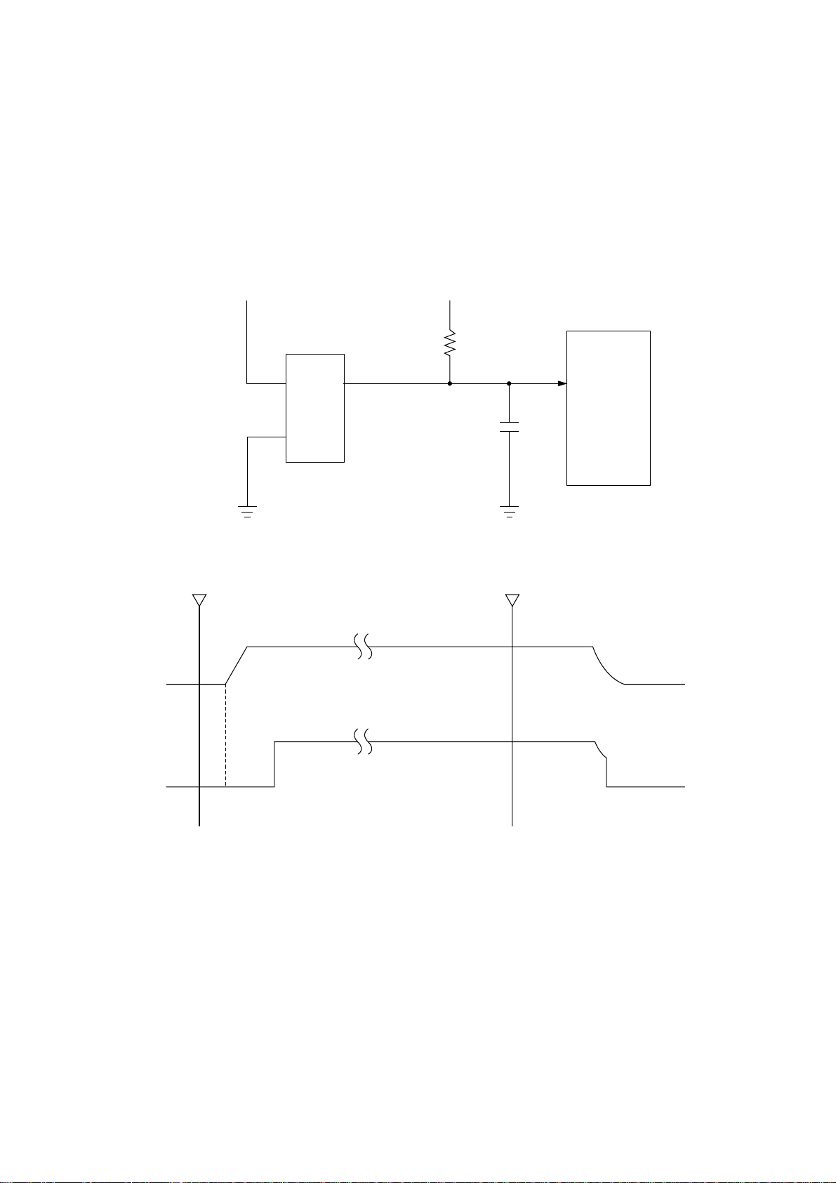
3.6 LED Lamp Control
There is an LED lamp on the high voltage power supply board which is connected to and controled
by the CPU on the main control board.
The light from the LED lamp can be seen on the Lens Cover through the LED Lens.
CN1
main control board high voltage power supply board
CPU
LED-P
41
CN1
- 9 -
Page 13
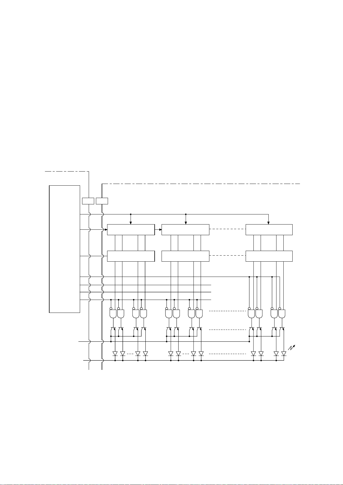
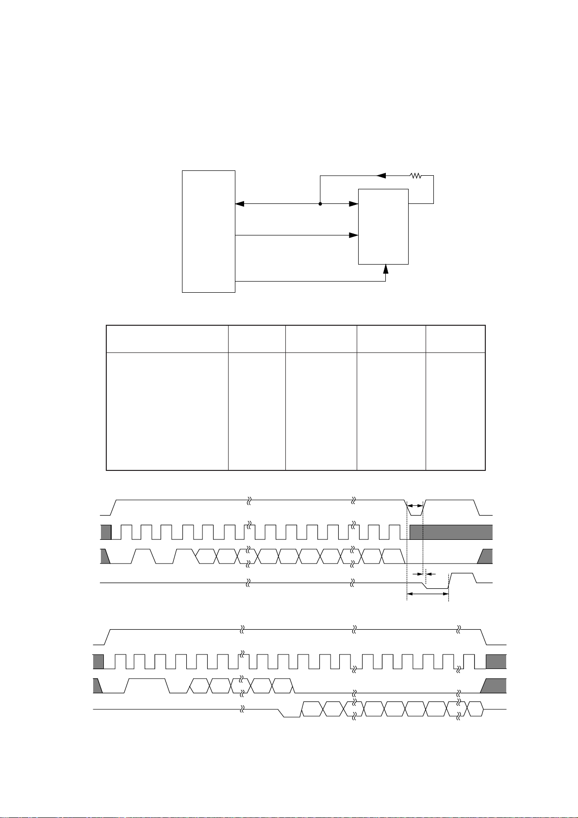
3.7 LED Head Control
When a paper form is made to arrive at the data write position on print start, the sending of data
to the LED head starts as synchronized with the page synchronous signal/line synchronous signal
(CPU internal signal).
Bit image data developed on the raster buffer in the CPU are DMA-transferred to the register of
a video interface controller (CPU built-in) and then sent to the shift register of the LED head in a
serial transmission synchronized with the VCLK-P signal by the VD0-P signal.
When 1-dot line data (2560 bits) is completely shifted, it is latched by means of the VLD-P signal,
causing LEDs to be driven by the VSTB1-N through VSTB4-N signals in different timing for each
signal.
Some of LED heads have 2496 dots rather than 2560 dots. The controls regarding the number
of dots are adjusted to the LED head installed when the printer is shipped from the factory.
Main control board
CPU
CN6 CN1
LED Head
VCLK-P
VD0-P
VLD-P
VSTB 1-N
VSTB 2-N
VSTB 3-N
VSTB 4-N
+5V
0V
90
89
91
92
93
94
95
Chip 40
64 bit shift REG
LATCH
Bit 2560
Chip 1
1 to 640 bits
641 to 1280
1281 to 1920
1921 to 2560
Bit 1
- 10 -
Page 14
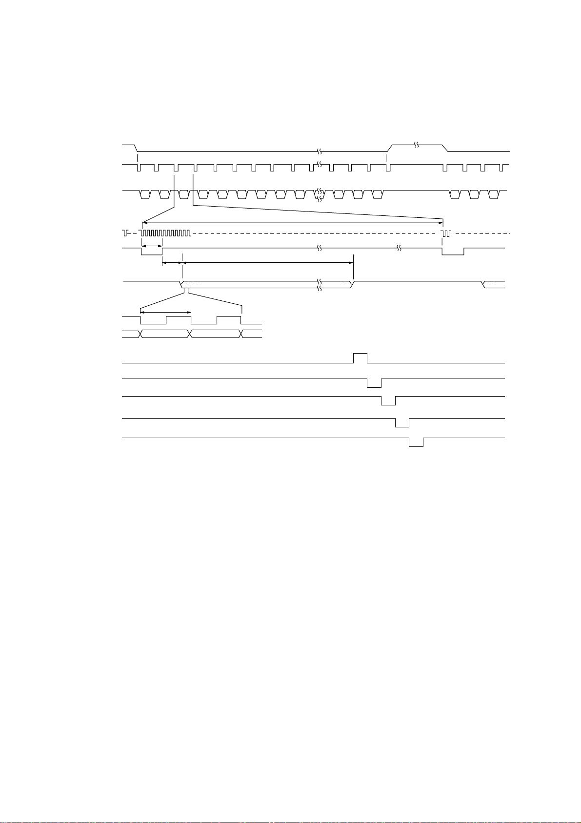
Page
synchronous
signal*
Line
synchronous
signal*
VDT-P
3.33 msec
VCLK-P
VDT-P
VCLK-P
VDT-P
VLD-P
VSTB1-N
VSTB2-N
VSTB3-N
VSTB4-N
* CPU internal signal
8 bits
8 bits
0.2 µs
2560 bits
- 11 -
Page 15
3.8 Motor and clutch control
The electromagnetic clutch is driven by a control signal from the CPU and the drive circuit shown
below.
The main motor is driven by the control signals from the CPU and the driver IC.
CPU
DMP1
DMP2
DMP3
96
97
98
Out4Vmm A Vmm B
Main Motor
8
ALARM
120 140
GATE CIRCUIT
ENA B
Signal of
DECACY
+5V
CN7
IC10
27
0V 0V
18
+5V
26
19
ENA A
To Out3, 4Logic
DECAY
37 1 1412 24
Out2 Out3
Out1
SW1 SW3
M
+24V OPEN
SW1 SW3
PHASE A PHASE B
GATE CIRCUIT
SW4SW2
SW4SW2
+5V
0V
25
BRUNK
OSC
Current
Q
-
R
+
S
Vref A Vref B
Sensor
Vs A Vs BRs A Rs BLG A PG LG B
23 22 28 15 10 21 20TAB5
Current
Sensor
RQ
+
S
0V
+5V
16
17
RMON
(1) Main motor
DMON-P
DMPH1-P
DMPH2-P
Rotation
+5V +24V
0V
99
0V
T0 T1 T2 T3
Forward rotation
CN8
Electromagnetic clutch
0VP
Reverse rotationStop
Operation at normal speed: T0 to T3 = 1.515 ms
- 12 -
Page 16
(2) Motor drive control
Time T0 to T3 determines the motor speed, while the phase different direction between
phase signals DMPH1-P and DMPH2-P determines the rotation direction. DMON-P signal
control a motor coil current. According to the polarity of the phase signal, the coil current flow
as follows:
1) +24V → SW1 → motor coil → SW4 → resistor → earth, or,
2) +24V → SW3 → motor coil → SW2 → resistor → earth
The drop voltage across the resistor is input to comparator, where it is compared with a
reference voltage. If an overcurrent flows, a limiter operates to maintain it within a certain
fixed current.
(3) Electromagnetic clutch control
Mechanical operation mode is switched by the combination of the clutch status and the
direction of motor rotation.
clutch status
off
off
on
on
rotation direction
Forward
Reverse
Forward
Reverse
operation mode
cleaning
Hopping from manual
feed slot
illegal operation
Hopping from tray
- 13 -
Page 17
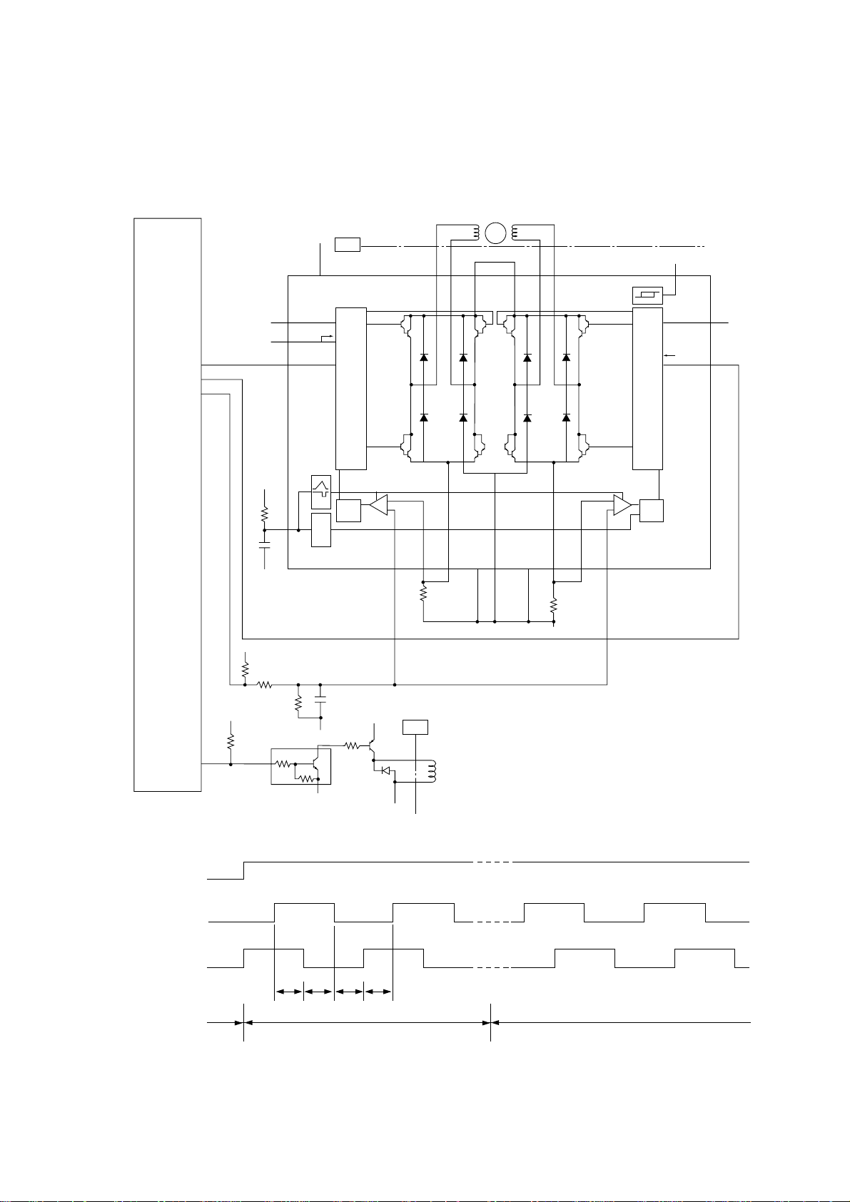
3.9 Fuser Temperature Control
The temperature change in a heat controller is converted into the electric potential TEMP
corresponding to the change in the resistance value of a thermistor, and the resultant potential
is fed back to the control circuit. The CPU performs ON/OFF control of the HEATON-P signal to
keep the heat roller temperature constant in accordance with the state at which the thermistor
voltage (TEMP) is read into directly by the AD converter of the CPU.
THCHK-N signal is fixed to “0”.
When the paper thickness is set on the menu of the host, the temperature is adjusted to the
targeted thickness accordingly.
Main Control Board
CPU
TEMP
27
AI4
(A/D)
THCHK-N
34
85
HEATON-P
High voltage power
supply board
IC20
5
+
6
-
7
+5V +5V
IC20
3
+
2
-
1
+5V
Thermistor
HEATON-N
Heater
Thermostat
Heat Roller
+5V
ACIN
Power supply unit
- 14 -
Page 18

Flowchart of Thermistor Circuit Check
START
HEATER OFF
Short check timer(t16)set
No
Time-out ?
Short error TEMP ?
Thermistor error check
timer (t2) set
Thermistor disconnection
check timer (t35) set
Heater On
Temperature > Tn
No
No
Yes
Yes
Yes
Tn...T0 =
T2 =
T4 =
Thermistor short error
End
Light
Medium
Heavy
To constant
temperature control
Thermistor
error check timer (t2)
within time
Yes
Thermistor
disconnection check timer
(t35) within time
Yes
t2 =
t16 =
t35 =
90 sec
520 msec
10 sec
No
No
Time-out
A/D value changed?
Yes
- 15 -
No
Fuser error
End
Thermistor disconnection
error
End
Page 19

Temperature
Controlled
Temperature
T
HEATER ON
OFF
Time
Temperature table
THCHK-N
O
Z
Heater control mode
Normal operation
Not used
T
145˚C:
150˚C:
155˚C:
160˚C:
165˚C:
Paper Thickness
light
medium light
medium
medium heavy
heavy
- 16 -
Page 20

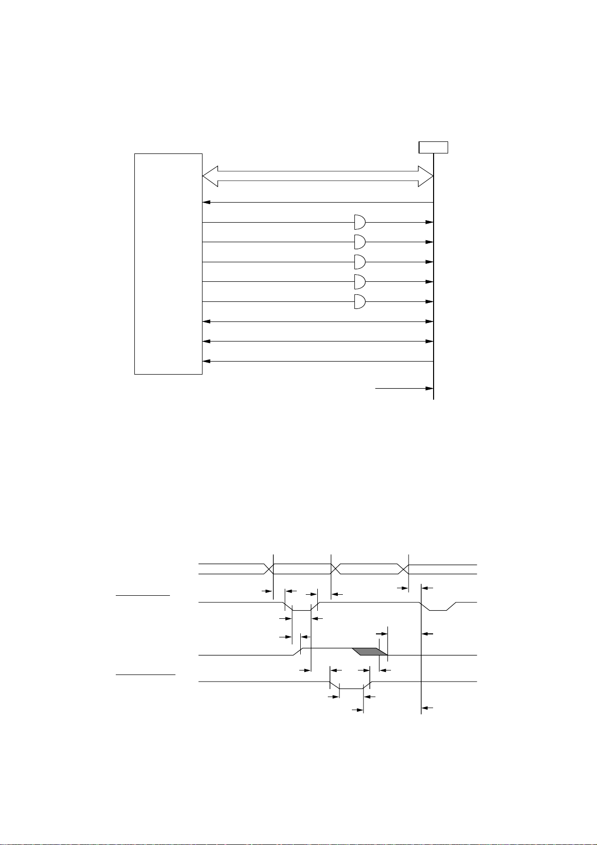
3.10 Sensor Control
The CPU supervises the state of each sensor every 40 ms.
Main Control Board High Voltage Power Supply Board
CN1 CN1
+5V
CPU
Sensor
signal
47
44
46
48
OFF
+5V
+5V
+5V
+5V
TNRSNS-N
PSIN-N
PSOUT-N
WRSNS-N
TransparentShield
PS1
PS2
PS3
PS4
ON
- 17 -
Page 21

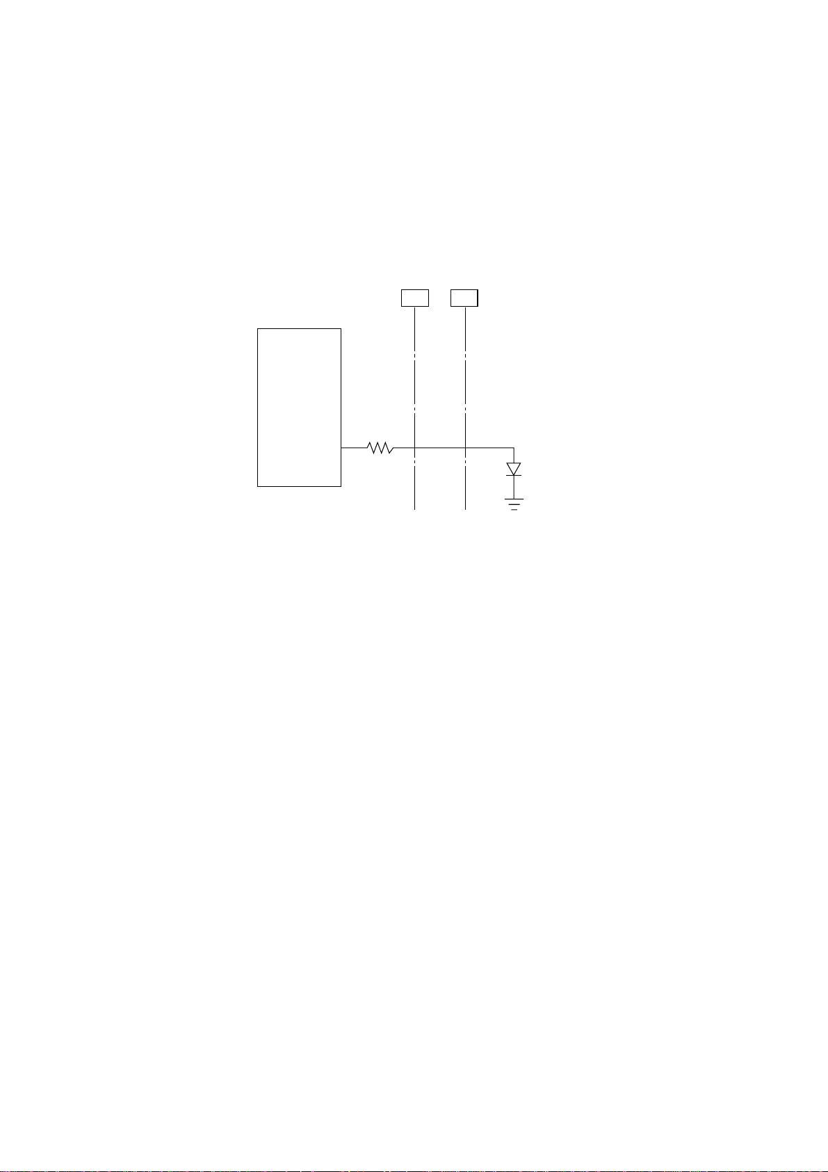
3.11 Cover Open
When the cover is opened, a cover open microswitch is opened. This makes a CVOPN-N signal
low, thereby the CPU detects that cover is open. Furthermore, opening the cover stops applying
a +5V power to the high voltage power supply part, resulting in stopping all high voltage outputs.
CN1 CN1
CVOPN-N
Main Control Board
45
CPU
+5V
0V
High Voltage Power Supply Board
CVOPN-N
+5V
+5V
Cover
Open
Microswitch
Cover close Cover open
High
Voltage
Power
Supply
Part
High
voltage
output
- 18 -
Page 22

3.12 Power Supply Part
(1) Power supply unit
An AC power from an inlet is input to Switching Reg. part .AC power is converted to a +24
VDC output and +5 VDC output.
ACIN
F1 F2L
FG
N
Circuit
Filter
Power supply unit
+24V
+5V
0V
Switching Reg. Part
HEATON-N
to AC output
Fuse Ratings
AC Input
Fuse
F1
F2
HEATER
CONTROLER
230 V
250 V 6.3 A
250 V 2 A
120 V
125 V 10 A
250 V 2 A
(2) High voltage power supply board
The +5 VDC power supplied to the high voltage power supply part via the cover open
microswitch as source voltage. The high voltage power supply part supplies necessary
voltage for electro-photography print to output terminals CH, DB, SB, TR, and CB according
to a control signal from the CPU. The table on the next page shows the relationship between
control signals and high voltage outputs.
CN1
MainControl Board High Voltage Power Supply Board
TR1PWM-P
55
TR2PWM-P
59
CHPWM-P
56
SDB1-P
53
CPU
52
54
SDB2-P
DBPWM-P
CVOPN-N
45
CN1
High Voltage
Power Supply
Part
CH
DB
SB
TR
CB
Cover Open
Microswitch
+5V
- 19 -
Page 23

Control Signals and High Voltage Outputs
Control signal name Level Function
TR1PWM-P
TR2PWM-P
CHPWM-P
SDB1-P
SDB2-P
DBPWM-P
H/L
(PWM)
L
H/L(PWM)
L
H/L(PWM)
L
H
L
H
L
H/L(PWM)
L
Makes the part put out a power to TR.
+3 to 5 µA
+0.5 to 4 KV
Makes the part put out a -750V power to TR.
Makes the part put out a -1.35 KV power to CH.
Makes the part put out the following power:
+450V or 0V power to SB
+300V power to DB
Makes the part put out the following power:
-450V power to SB
-300V power to DB
+400V power to CB
Makes the part put out the power to SB, DB, CB.
- 20 -
Page 24

4. TROUBLESHOOTING
4.1 Troubleshooting Table
(A) High Voltage Power Supply Board
Note:
A malfunction of the power supply is not repaired by an agency. The abnormality to be
treated here is that of sensors only.
Failure PC Display Message
A paper input jams occur frequently.
PAPER
Flowchart
No.
A - 1
INPUT JAM
A paper feed jams occur frequently.
PAPER
A - 2
FEED JAM
A paper-exit jams occur frequently.
PAPER
A - 3
EXIT JAM
A paper size errors occur frequently. A - 4
PAPER
SIZE ERROR
Paper can not be fed from the manual feed slot . A - 5
The message "COVER OPEN" remains displayed on
the PC display.
COVER OPEN
A - 6
The message "TONERLOW" remains displayed on
the PC display.
The message "TONERSNS" remains displayed on
the PC display.
TONER LOW
TONER SENSOR
- 21 -
A - 7
A - 8
Page 25

(B) Main Control Board
Failure PC Display Message
Initialization error and not restored
INITIALIZATION
Flowchart
No.
B - 1
ERROR
Program ROM error
ROM CHECK
B - 2
ERROR
Resident RAM error
RAM CHECK
B - 3
ERROR
EEPROM error B - 4
EEPROM CHECK
ERROR
Fuser error B - 5
Watchdog timer timeout occurs frequently. B - 6
FUSER ERROR
WATCHDOG
Data sent through the Parallel I/F cannot
be received.
TIMER ERROR
INITIALIZATION
ERROR
B - 7
- 22 -
Page 26

4.2 Troubleshooting Flowchart
A-1 Paper input jams occur frequently.
• Is PS4 (Write Sensor ) operating normally?
• No Replace PS4.
▼
• Yes Is Pin1 of CN8 in main control board operating normally?
• No Replace Q4 or Q5 in main control board.
▼
• Yes Failure of IC6 (MSM65917) in main control board.
A-2 A paper feed jams occur frequently.
• Is PS4 (Write Sensor ) operating normally?
• No Replace PS4.
▼
• Yes Is PS3 (Outlet Sensor ) operating normally?
• No Replace PS3.
▼
• Yes Failure of IC6 (MSM65917) in main control board.
A-3 A paper exit jams occur frequently.
• Is PS3 (Outlet Sensor) operating normally?
• No Replace PS3.
▼
• Yes Failure of IC6 (MSM65917) in main control board.
A-4 A paper size errors occur frequently.
• Is PS4 (Write Sensor ) operating normally?
• No Replace PS4.
▼
• Yes Failure of IC6 (MSM65917) in main control board.
A-5 Paper can not be fed from manual feed slot.
• Is PS2 (Manual Feed Sensor) operating normally?
• No Replace PS2.
▼
• Yes Failure of IC6 (MSM65917) in main control board.
- 23 -
Page 27

A-6 The message “COVER OPEN” remains displayed on the PC display.
• Is CVSW (Cover Open Switch) operating normally?
• No Replace CVSW.
▼
• Yes Failure of IC6 (MSM65917) in main control board.
A-7 The message “TONERLOW” remains displayed on the PC display.
• Is PS1 (Toner Sensor) operating normally?
• No Replace PS1.
▼
• Yes Failure of IC6 (MSM65917) in main control board.
A-8 The message “TONERSNS” remains displayed on the PC display.
• Is PS1 (Toner Sensor) operating normally?
• No Replace PS1.
▼
• Yes Failure of IC6 (MSM65917) in main control board.
- 24 -
Page 28

B-1 Initialization error and not restored
• Replace IC2.
▼
• OK?
▼
• No Is the 10-MHz clock signal being put out to pin 3 of OSC1?
• No Replace OSC1 (CST 10.0MTW).
▼
• Yes Failure of IC6 (MSM65917)
B-2 Program ROM error
• Replace IC2.
B-3 Resident RAM error
• Are negative pulses being put out to Pin 4 , 23 (RAS0-N , CAS-N) of IC11?
• No Failure of IC6 (MSM65917)
▼
• Yes Are the signals at pins, 9 TO 12 , 14 TO 18 , 5
(DA00-P to DA09-P) of IC11 being changed?
• No Failure of IC6 (MSM65917)
▼
• Yes Replace IC11.
B-4 EEPROM error
• Replace IC4.
▼
• OK?
▼
• No Failure of IC6 (MSM65917)
B-5 Fuser error
• Is the heater on?
▼
• No Is the voltage at Pin 40 (HEATON-P) of IC6(MSM65917) 5V?
• Yes Replace Q3 or IC20
▼
• No Failure of IC6 (MSM65917)
B-6 Watchdog timer timeout occurs frequently.
• Replace IC2.
▼
• OK?
▼
• No Failure of IC6 (MSM65917)
- 25 -
Page 29

B-7 Data sent through the Parallel I/F cannot be received.
• Is the signal at Pin 11 (BUSY-P) of CN4 being at low level?
• No Is the signal at Pin 13 (BUSY-P) of IC7 (7407) changed as shown
below, at data reception?
ON-LINE OFF-LINE
BUSY-P Low High
• No Failure of IC6 (MSM65917)
▼
• Yes Replace IC7 (7407).
▼
• Yes Is the level of the signal at Pin 1 (STB-N) of CN4 changed at data reception?
• No Make sure of the connection of I/F cable or the operation of the h ost
computer.
▼
• Yes Are the signals at Pin 1 (ACK-N), Pin 9 (FAULT-N) of IC7 (7407) being
respectively at low level and high level in on-line mode?
• No Replace IC7 (7407).
• OK?
▼
▼
• Yes Failure of IC6 (MSM65917)
• No
- 26 -
Page 30

5. CIRCUIT DIAGRAM
Figure5-1~5-7 Main Control PCB (HBMC or HBMC-2) Circuit Diagram (Rev. 4)
Figure5-8 High voltage Power Supply PCB (OLHV-) Circuit Diagram (Rev.7)
(TLHV-) Circuit Diagram (Rev.3)
- 27 -
Page 31

A
+5V
+5V
IC5
Not Mounted (HIGH-LEVEL)
Mounted (LOW-LEVEL)
0V
0V
0V
CH1
0V
0V
+5V
NOMOUNT
NOMOUNT
NOMOUNT
NOMOUNT
NOMOUNT
NOMOUNT
NOMOUNT
NOMOUNT
NOMOUNT
NOMOUNT
SIGNAL
OPEN
EAN
Pin-No Short-Wire
MSM65917 Mode change
Tool not connected
Tool connected
Internal ROM External ROM External ROM
61 R53
SP1 B Side A Side A Side62
OSC1
R510
R53
1
1
0
2
2
13
2
1
1
1
2
R533
C15
0.1µ 50
5.1K 0.1
112
R52
0
0
12
R51
3.6K 0.1
12
R50
12
2
C14
0.1µ 50
1
2
C12
0.1µ 50
1
2
C13
0.1µ 50
1
2
C509
0.1µ 50
1
2
C503
0.1µ 50
1
2
C511
0.1µ 50
1
2
C510
0.1µ 50
2
1
C514
0.1µ 50
1
2
C504
0.1µ 50
2
1
C513
0.1µ 50
1
2
R511
12
3
3
141824231720192122
131211
10
151635
36
3738394349
3442408586
41
105
102
976
5
8
87
1
111
CH5
CH4CH6CH7
11
CH2 CH3
2
4
1
606162
63
454746
48
27282930312632
7670585125
7569575033
44
106
104
103
108
107
PST592
VCC
GND
OUT
CST10.0MTW
CST
0
R526
12
150 0.1
10K 0.1
CH8
SP1 (Short-plug)
SP1 SP1 SP1
123
AB
(074G) CVOPN-N
(076F) TNRSNS-N
(076G) WRSNS-N
(076G) PSOUT-N
(076F) PSIN-N
(065D) DIPSW2
(065D) DIPSW1
(075F) TEMP
(016F) THCHK-N
(075E) TR-VSEN
(075E) TR-ISEN
GND1
GND2
GND3
GND4
GND5 PU00
P40
P41
P42
P43
P44
P45
P46
P20
P21
P24
P25
P27
INT0
INT1
WRN
RDN
ALE
AD0
AD1
AD2
AD3
AD4
AD5
AD6
AD7
A8
A9
A10
A11
A12
A13
A14
A15
ROCS
CPCK
65917
(1/2)
GND6
GND7
VDD1
VDD2
VDD3
VDD4
VDD5
VDD6
VDD7
AGND
AVDD
AI0
AI1
AI2
AI3
AI4
P30
P31
P32
P33
P34
P35
P36
P37
RSTN
EAN
CPEN
TEST
OSC0
OSC1
IC6
CHPW
DBPW
T2PW
T1PW
SDB2
SDB1
RMON
RMP1
RMP2
DMON
DMP1
DMP2
VSB4
VSB3
VSB2
VSB1
VLDP
VCLK
VD0P
VD1P
FLTN
SELP
PEP
BSYP
ACKN
DWRN
CASN
RAS0
RAS1
RAS2
DA7
DA6
DA5
DA4
DA3
DA2
DA1
DA0
DA10
DA9
DA8
65917
(2/2)
PSBN
AFXN
SLIN
IPRN
PDT2
PDT1
PDT3
PDT4
PDT5
PDT6
PDT7
PDT8
DD0
DD3
DD2
DD1
IC6
LED-P (073E)
XCLK-P (065B)
HEATON-P (076D)
FANALM-N (03XG)
EEPRMDT-P (047A)
EEPRMCS-P (047B)
EEPRMCLK-P (048C)
AD00-P (027B)
AD01-P (027B)
AD02-P (027B)
AD03-P (027B)
AD04-P (027B)
AD05-P (027B)
AD06-P (027B)
AD07-P (027B)
A08-P (02XB)
A09-P (02XB)
A10-P (02XB)
A11-P (02XB)
A12-P (02XB)
A13-P (02XB)
A14-P (02XB)
A15-P (02XB)
ROMCS-N (02XC)
RD-N (02XC)
ALE-P (027C)
FANON-P (037E)
DCLED-P (071F)
THCHK-N (013E)
TXD-P (065B)
BANK (02XB)
RXD-P (065B)
5352555954
56
99
100
101
989697
92939495919089
88
8180797877
120
125
126
127
128
119
118
117
116
115
114
113
112
111
110
109
123
124
121
122
7473727168676665828384
64
(024B) DD01-P
(024B) DD00-P
(024C) DD03-P
(024C) DD02-P
(054B) PDATA8-P
(054B) PDATA7-P
(054B) PDATA6-P
(054C) PDATA5-P
(054C) PDATA4-P
(054C) PDATA3-P
(054C) PDATA2-P
(054C) PDATA1-P
(054E) IPRIME-N
(054F) SELIN-N
(054G) AUTOFD-N
(054E) PSTB-N
DA10-P (024A)
DA09-P (022C)
DA08-P (022C)
DA07-P (022C)
DA06-P (022C)
DA05-P (022C)
DA04-P (022C)
DA03-P (022C)
DA02-P (022D)
DA01-P (022D)
DA00-P (022D)
RAS2-N (025D)
RAS1-N (025E)
RAS0-N (023E)
CAS-N (023E)
DWR-N (022D)
ACK-N (057E)
BUSY-P (057D)
PE-P (057E)
SEL-P (057F)
FAULT-N (057F)
VD1-P (041B)
VD0-P (041B)
VCLK-P (041B)
VLD-P (041C)
VSTB4-N (041D)
VSTB3-N (041D)
VSTB2-N (041C)
VSTB1-N (041C)
PJON-P (037B)
CHPWM-P (071D)
DBPWM-P (071B)
TR2PWM-P (071E)
TR1PWM-P (071C)
SDB2-P (071B)
SDB1-P (071A)
DMPH1-P (033C)
DMON-P (031D)
DMPH2-P (033C)
B
C
D
E
F
G
H
Y
Y
(HBMC- or HBMC-2 1/7) Rev. 4
Circuit Diagram
Figure 5-1 Main controller PCB
456 879X
3
2
1
A
B
C
D
- 28 -
E
F
3456 879X
2
1
G
H
Page 32

A
+5V
+5V
+5V
0V
0V
0V
0V
CN9
Option-RAM
(01XB) DA10-P
(018B) DD00-P
(01XB) DA09-P
(01XC) DA08-P
(01XC) DA07-P
(01XC) DA06-P
(01XC) DA05-P
(01XC) DA04-P
(01XC) DA03-P
(01XC) DA02-P
(01XC) DA01-P
(01XC) DA00-P
(01XD) DWR-N
(018B) DD01-P
(018C) DD02-P
(018C) DD03-P
DRAM-A10
DRAM-A09
DRAM-A08
DRAM-A07
DRAM-A06
DRAM-A05
DRAM-A04
DRAM-A03
DRAM-A02
DRAM-A01
DRAM-A00
DRAM-D03
DRAM-D02
DRAM-D01
DRAM-D00
RAS2N
RAS1N
CASN
DRAM-WRNOEVCC
VCC
VCC
GND
GND
GND
GND
GND
GND
GND
GND
GND
CN924CN925CN926CN927CN928CN929CN930CN912CN9
11
21
CN910CN99CN93CN92CN97CN9
6
CN9
8
CN91CN94CN9
5
CN919CN917CN918CN913CN914CN915CN9
16
CN920CN922CN923CN931CN932CN9
R548
1
2
0
R546
1
2
0
R549
1
2
0
R550
1
2
0
IC11
A9A8A7A6A5A4A3A2A1A0WEOEVCC
VSS
RAS CAS
I/O4
3
22
13
423
1
2
24
25
26
5
18171615141211
10
9
I/O3
I/O2
I/O1
514400J
C520
0.1µ 50
1
2
R547
100
12
(01XD) RAS0-N
(01XD)CAS-N
(01XC) RAS2-N
(01XC) RAS1-N
<512>
<128>
DQ1DQ1
DQ2DQ2
WEWE
RASRAS
NCA9
A0A0
A1A1
A2A2
A3A3
Vcc
1
2
3
4
5
9
10
11
12
13
26
25
24
23
22
18
17
16
15
14Vcc
VssVss
DQ4DQ4
DQ3DQ3
CASCAS
OEOE
A8A8
A7A7
A6A6
A5A5
A4A4
IC11
1M Mask
27C1001
27512
IC2
123 (1)
4 (2)
5 (3)
6 (4)
7 (5)
8 (6)
9 (7)
10 (8)
11 (9)
12 (10)
13 (11)
14 (12)
15 (13)
16 (14)
NC
A16
A15
A12A7A6A5A4A3A2A1A0D0D1D2GND
VPP
A16
A15
A12A7A6A5A4A3A2A1A0DOD1D2GND
--A15
A12A7A6A5A4A3A2A1A0DOD1D2GND
--VCC
A14
A13A8A9
A11
OE/VPP
A10CED7D6D5D4D3
VCC
PGMNCA14
A13A8A9
A11OEA10CED7D6D5D4D3
VCCNCNC
A14
A13A8A9
A11
OE/OE
A10
CE/CED7D6D5D4
D3
32
31
(28) 30
(27) 29
(26) 28
(25) 27
(24) 26
(23) 25
(22) 24
(21) 23
(20) 22
(19) 21
(18) 20
(17) 19
(16) 18
(15) 17
GND
VCCNCVPPCEOE
PGM
A0A1A2A3A4A5A6A7A8A9A10
A11
A12
A13
A14
A15
A16 Q7
21
3124221303216
2
3
29
284252326
27
56789
101112
20191817151413
Q6Q5Q4Q3Q2Q1Q0
(016E) RD-N
C501
0.1µ 50
1
2
(016C) ROMCS-N
Vcc=+5V, Ground=0V
SOCKET
IC2
IC3
27C1001
74LS373
1D
2Q3Q4Q5Q6Q7Q8Q
1Q
2D3D4D5D6D7D8DENOC
2
1
1118171413
874
3
569
121516
19
(016D) AD07-P
(016F) BANK
(016C) A15-P
(016C) A14-P
(016C) A13-P
(016C) A12-P
(016C) A11-P
(016C) A10-P
(016C) A09-P
(016C) A08-P
(016D) AD06-P
(016D) AD05-P
(016D) AD04-P
(016D) AD03-P
(016D) AD02-P
(016D) AD01-P
(016D) AD00-P
(016E) ALE-P
B
C
D
E
F
G
H
Y
Y
(HBMC- or HBMC-2 2/7) Rev. 4
Circuit Diagram
Figure 5-2 Main controller PCB
456 879X
3
2
1
A
B
C
D
E
F
G
H
3456 879X
2
1
- 29 -
Page 33

A
NOMOUNT
NOMOUNT
CH10CH9
11
CN7
4M-DMOTOR
IC10
+5V
(01XF) DMON-P
R542
1K 0.1
12
R541
C524
22K
50
2200p
0.1
112
R540
C523
C4
4.3K
0.1µ 50
47µ 50
0.1
1
1
21
+
2
2
2
R543
12
22K 0.1
0V
0V
0V
C525
12
0.1µ 50
+5V
+24V
ZA21
ZA20
1
1
0Vp
30
NC6
13
11
964
2
10
5
24
12
8
7
3
NC5
NC4
NC3
NC2
NC1
RSB
RSA
NALM
OUT4
OUT3
OUT2
OUT1
29
14
1
15
28
19
18
21
20
22
23
25
16
17
27
26
GND2
GND1
VMM2
VMM1
LGB
LGA
VCC
DCAY
VSB
REFB
REFA
CR
NENB
NENA
PHAB
PHAA
VSA
MTD2005F
CN71CN72CN73CN7
4
IM=0.38A
R1
1
2 0.5
2
R2
1
2 0.5
2
0Vp
DMPH2-N
DMPH2-P
DMPH1-N
DMPH1-P
+5V
R54
1
1K
6.2K
0.1
2
R55
1
0.1
2
(01XF) PJON-P
(016E) FANON-P
Q5
22K
22K
2
3
1
0V
OVP
+24V
CN8
2M-PJ
Q4
3
3
2SA1338
SS100MA80VACP
221
1
D3
CN8
1
CN8
2
PJON
OVP
NOMOUNT
CN3
2M-Fan
NOMOUNT
NOMOUNT
NOMOUNT
NOMOUNT
NOMOUNT
2
2
2
22K
22K
1
1
3
R502
Q502
10K 0.1
+24V
Q501
3
3
112
2SA1338
0V
D501
SS100MA80VACP
FANPOW
R5011
10K 0.1
2
0VP
0VP
+5V
FANALM-N FANALM-N (016F)
CN3
1
CN3
2
CN3
3
(01XF) DMPH1-P
(01XF) DMPH2-P
0V
B
C
D
E
F
G
H
Y
Y
(HBMC- or HBMC-2 3/7) Rev. 4
Circuit Diagram
Figure 5-3 Main controller PCB
456 879X
3
2
1
A
B
D
C
- 30 -
E
F
3456 879X
2
1
G
H
Page 34

A
+5V
R520
12
330
R519
NOMOUNT
12
330
R513
12
330
R512
12
0
(01XE) VD0-P
(01XE) VD1-P
(01XE) VLD-P
(01XE) VCLK-P
(01XF) VSTB1-N
(01XE) VSTB2-N
(01XE) VSTB3-N
(01XE) VSTB4-N
SS100MA80VACP SS100MA80VACP
NOMOUNT
NOMOUNT
NOMOUNT
NOMOUNT
SS100MA80VKCP SS100MA80VKCP
D1 D2
1
3
2
1
3
2
CN6
14F-LED
CN66CN67CN68CN69CN610CN611CN612CN6
13
CN6
3
CN6
4
CN6
5
HDDT0-P
HDDT1-P
HDCLK-P
HDLD-P
STB1-N
STB2-N
STB3-N
STB4-N
D4
1
3
2
D5
1
3
2
0V
5V
5V
0V
CN6
1
0VP
CN6
2
0VP
CN6
14
FG
+5V
11+2
2
C526
C1
0.1µ
3300µ
50
12
C16
0.01µ 250
12
C8
0.01µ 250
10
0V
0VP
FG1
FG2
FG
1
1
(016E) EEPRMDT-P
(016E) EEPRMCS-P
(016E) EEPRMCLK-P
+5V
R537
C522
0.1µ 50
5.1K 0.1
112
R538
5.1K 0.1
12
R539
10K 0.1
12
2
0V
3261857
IC4
93LC46
DIDONC1C8VCC
GND1
NC2
4
0V
B
C
D
E
F
G
H
Y
Y
(HBMC- or HBMC-2 4/7) Rev. 4
Circuit Diagram
Figure 5-4 Main controller PCB
456 879X
3
2
1
A
B
C
D
- 31 -
E
F
G
H
3456 879X
2
1
Page 35

A
+5V
CN4
36F-Centro
PDATA8-P
CN4
9
PDATA7-P
CN4
8
PDATA6-P
CN4
7
PDATA5-P
CN4
6
PDATA4-P
CN4
5
PDATA3-P
CN4
4
PDATA2-P
CN4
3
PDATA1-P
CN4
2
STB-N
CN4
1
IPRIME-N
CN4
31
SELIN-N
CN4
36
AUTOFEED-P
CN4
14
R30
21
22 0.1
R31
21
22 0.1
R29
21
22 0.1
R28
21
22 0.1
R25
21
22 0.1
R26
21
22 0.1
R27
21
22 0.1
R24
21
22 0.1
R528
12
100 0.1
R514
21
1K 0.1
R505
12
3.3K 0.1
R515
12
3.3K 0.1
R522
1
10K 0.1
R521
12
10K 0.1
R527
21
1K 0.1
R506
C515
560p 50
112
2
C506
1000p 50
1
2
C507
560p 50
1
2
C508
560p 50
1
2
1K 0.1
R504
12
1K 0.1
R516
3.3K 0.1
21
R509
3.3K 0.1
21
R507
3.3K 0.1
21
R508
3.3K 0.1
21
R517
3.3K 0.1
21
R518
3.3K 0.1
21
R524
3.3K 0.1
21
R523
3.3K 0.1
21
PDATA8-P(018D)
PDATA7-P (018D)
PDATA6-P(018D)
PDATA5-P (018D)
PDATA4-P(018D)
PDATA3-P (018D)
PDATA2-P(018D)
PDATA1-P (018D)
+5V
0V
0V
0V
0V
+5V
+5V
NOMOUNT
NOMOUNT
Vcc=+5V , Ground=0V
OC
56
IC7
07
AUTOFD-N (018E)
SELIN-N (018E)
IPRIME-N (018E)
PSTB-N (018E)
+5V
+5V
0V
C505
R38
0.1µ 50
112
2
3.3K 0.1
R37
12
3.3K 0.1
R35
12
3.3K 0.1
R36
12
3.3K 0.1
R43
12
3.3K 0.1
R44
12
3.3K 0.1
(01XE) BUSY-P
(01XE) ACK-N
(01XE) PE-P
(01XE) SEL-P
(01XE) FAULT-N
Vcc=+5V , Ground=0V
Vcc=+5V , Ground=0V
Vcc=+5V , Ground=0V
Vcc=+5V , Ground=0V
Vcc=+5V , Ground=0V
OC
13 12
07
IC7
OC
12
07
IC7
OC
34
07
IC7
OC
11 10
07
IC7
OC
98
07
IC7
FG
C7
0.01µ
250
12
C17
0.01µ
250
12
0V
+5V
R42
12
0
CN4
38
FG
CN4
37
FG
CN4
17
FG
CN4
18
5V
CN4
32
FAULT-N
CN4
13
SEL-P
CN4
12
PE-P
CN4
10
ACK-N
CN4
11
BUSY-P
CN4
35
HILEVEL
CN4
34
N/C
CN4
15
N/C
CN4
33
SG
CN4
30
SG
CN4
29
SG
CN4
28
SG
CN4
27
SG
CN4
26
SG
CN4
25
SG
CN4
24
SG
CN4
23
SG
CN4
22
SG
CN4
21
SG
CN4
20
SG
CN4
19
SG
CN4
16
SG
0V
CN4
36F-Centro
B
C
D
E
F
G
H
Y
Y
(HBMC- or HBMC-2 5/7) Rev. 4
Circuit Diagram
Figure 5-5 Main controller PCB
456 879X
3
2
1
A
B
C
D
- 32 -
F
E
G
H
3456 879X
2
1
Page 36

A
+5V
NOMOUNT
NOMOUNT
NOMOUNT
NOMOUNT
NOMOUNT
NOMOUNT
NOMOUNT
NOMOUNT
NOMOUNT
NOMOUNT
NOMOUNT
NOMOUNT
NOMOUNT
NOMOUNT
NOMOUNT
NOMOUNT
NOMOUNT
NOMOUNT
NOMOUNT
NOMOUNT
NOMOUNT
IC9
OSC
VOUT
LV
CAP+
CAP-
GND
V+
C512
21
1000p 50
8
756
2
4
3
C6
10µ 16
21+
C5
C516
10µ
0.1µ 50
16
221
1
C517
0.1µ 50
21
+
0V
0V
0V
SW1
2
1
3
4
2
1
DIPSW2 (014D)
DIPSW1 (014D)
+5V
RXD-P (01GF)
R525
12
20 0.1
R532
12
20 0.1
R534
12
20 0.1
R530
12
20 0.1
(016F) TXD-P
(016F) XCLK-P
(06XE) RXD+
(06XF) RXD-
2
IC8
3
4
12
151413
567
11
10916
8
1
7660
DS8925
DIN1
DIN2
RIN1-
RIN2+
RIN2-
RIN3+
VCC
GND
VEE
DEN1
DOUT1+
DOUT1-
DOUT2-
ROUT1
ROUT2
ROUT3
0V
0V
0V
0V
C521
150p 50
1
2
C518
150p 50
1
2
C519
150p 50
1
2
CN5
TCS7187-01-201
CN5
6
TXD+
CN5
3
TXD-
R529
12
20 0.1
R544
12
0
R536
12
0.1200
200
R535
12
0.1
R531
12
20 0.1
CN5
1
XCLK-N
CN5
7
+5V
CN5
4
CN5
8
SG
+5V
RXD+
CN5
5
RXD-
CN5
2
CN5
FGFGFG
FG
9
CN510CN5
11
HSK-IN
RXD+ (065B)
RXD- (065B)
B
C
D
E
F
G
H
Y
Y
(HBMC- or HBMC-2 6/7) Rev. 4
Circuit Diagram
Figure 5-6 Main controller PCB
456 879X
3
2
1
A
B
C
D
- 33 -
E
F
3456 879X
2
1
G
H
Page 37

A
CN1
High-voltage
(01XG) SDB1-P
(01XG) SDB2-P
(01XG) DBPWM-P
(01XG) TR1PWM-P
(01XF) CHPWM-P
(01XG) TR2PWM-P
(016F) DCLED
R39
R40
C11
1122
1K 0.1
R5
12
0
OC
NOMOUNT
LS07
1
1
2
2
34
0.11K
R41
1256
98
11 10
0.1300
R34
12
0.1220
R32
21
0.1300
R33
21
0.1300
R7
12
0
R9
12
0
R13
12
0
R11
12
0
R22
Q2
Q1
12
10K
2SA1338
0.1
0.047µ 50
C10
2
1
0.022µ 50
C18
2
1
0.022µ 50
C19
1
2
2
1
1
2
3
3
0.022µ 50
R3
12
0
OC
NOMOUNT
NOMOUNT
LS07
OC
LS07
NOMOUNT
OC
LS07
IC1
IC1
IC1
IC1
NOMOUNT
OC
LS07
IC1
13 12
NOMOUNT
NOMOUNT
NOMOUNT
NOMOUNT
NOMOUNT
NOMOUNT
NOMOUNT
NOMOUNT NOMOUNT
NOMOUNT
OC
LS07
IC1
Vcc=+5V , Ground=0V
22K
22K
0V
+24V
+5V
C9
0.1µ 50
12
0V
11
0V
CN1
10
0V
CN1
9
0V
CN1
7
0V
CN1
5
0V
CN1
17
5V
CN1
15
5V
CN1
23
CN1
CVOPN-N (014D)CVOPN-N
1
CN1
PSOUT-N PSOUT-N (014D)
16
CN1
WRSNS-N
19
CN1
PSIN-N
21
CN1
TNRSNS-N
13
CN1
6
CN122CN1
3
CN1
TEMP TEMP (013E)
TNRSNS-N (014D)
PSIN-N (014D)
WRSNS-N (014D)
(016G) LED-P LED-P
DCLED-P
+5V
12
R19
100K 0.1
21
R56
200K 0.1
12
R545
4.7K 0.1
12
R15
10K 0.1
12
R12
510 0.1
12
R14
510 0.1
12
R10
510 0.1
12
R8
3.3K 0.1
12
R4
3.3K 0.1
12
R6
3.3K 0.1
12
R16
10K 0.1
12
R17
10K 0.1
12
R18
10K 0.1
21
R20
1.2K 0.1
21
R21
1K 0.1
12
R503
10K 0.1
1
1
12+
2
2
R23
C502
C3
0.1µ 50
47µ 16
12+
C2
47µ 50
1K 0.1
TR-ISEN (014E)
TR-ISEN
12
CN1
4
CN1
TR-VSEN (014E) TR-VSEN
TR2PWM-P
2
CN1
CHPWM-P
8
CN1
TR1PWM-P
DBPWM-P
14
CN1
SDB2-P
20
CN1
SDB1-P
18
CN1
+5V
+5V
0V
0V
0V
0V
0V
+5V
+5V
+5V
+5V
3
2
4
1
8
+
-
5
6
4
7
8
+
-
(016F) HEATON-P
IC20
IC20
393
393
2.2K
10K
Q3
2
1
3
CN2
8
CN2
NC
7
CN2
0V
4
CN2
0V
3
CN2
5V
2
CN2
5V
1
CN2
0VP
5
CN2
24V
+24V
6
HEATON-N
1
0V
+5V
0VP
CN2
Power
B
C
D
E
F
G
H
Y
Y
(HBMC- or HBMC-2 7/7) Rev. 4
Circuit Diagram
Figure 5-7 Main controller PCB
456 879X
3
2
1
A
B
C
D
- 34 -
E
F
G
H
3456 879X
2
1
Page 38

A
10
DBPWM-P
SDB1-P
CN16CN1
SDB2-P
4
CN1
TR1PWM-P
16
CN1
TR2PWM-P
20
CN1
CHPWM-P
(017D) VSEN TR-VSEN
22
CN1
12
CN1
(01XE) ISEN TR-ISEN
21
CN1
(015G) TNRSNS TNRSNS-N
3
CN1
(015G) PSIN PSIN-N
5
CN1
(015G) WRSNS WRSNS-N
8
CN1
(015G) PSOUT
(012F) THERM TEMP
PSOUT-N
23
CN1
11
CN1
2
CN1
LED
1
CN1
7
CN19CN1
+5V
H5V
H5V
R118
CVOPN-N
12
G
G
G
G
G
5V
5V
4.7K 0.25
CVSW
1
3
2
N.O
N.C
LED-P
18
CN1
DCLED-P
13
CN1
0V
14
CN1
1
CN2
2
CN2
0V
15
CN1
0V
17
CN1
0V
19
CN1
0V
LED24V
12
SEL3910D-YZ
GND
GND
G
GND
CN3
1
GND
CN3
2
+5V
+5V
G
TH
5V
THERM (011D)
GND
GND
GND
GND
GND
GND
GND
H5V
H5V
GND
GND
H5V
G
R47
1
130 0.25
2
R48
C312
0.1µ 50
12
NOMOUNT
1
130 0.25
2
1
2
3
4
PS1
SG-206
1
2
3
4
PS2
SG-206
1
2
3
4
PS3
SG-206
1
2
3
4
PS4
SG-206
G
TNRSNS (011C)
PSIN (011C)
PSOUT (011C)
WRSNS (011C)
G
G
6
5
G
G
G
G
G
G
G
3
3
2
1
3
2
1
Q16
2
21
1
Q17
Q15
2SC2235-Y
2SC2235-Y
2SC2235-Y
D82
D62
C251
0.1µ 50
470p 3.15K
D76
RD27E-B1 RD22E-B
EU02A
EU02A
12
12
12
D71
112
2
1
1
2
2
C311
C117
R119
100M 0.5
0.1µ 50
1
2
C310
C114
C116
C115
D69 D68
D87
RD200E-B
R115
576K 0.25
C119
470p 1K
C301
C111
C302
D67
C112
C300
D61R234
33 0.25
R105
R122
C103
C104
D58
39p 500
470p 1K
C108
0.1µ50
0.1µ50
0.1µ50
0.1µ
50
10µ
63
5.1k 0.25
221
R123
1k 0.25
21
R124
R121
R229
D52
D55
D56
D85
D84
D83
D81
470V
Q11
C105
C241
C102
L10
C237
C236
1
1
12
+
2
2
1000µ
C-14576
1ZB300-Y/Z
5.1K 0.25
1
1
1
1
1
1
1
1
1
1
1122
2
2
2
2
2
2
2
2
3
2
2
2
R112
Q13
C240
C107
5.1k
BCR1AM-12
BCR1AM-12
CR04AM-12
1ZB300-Y/Z
0.25
5.1k 0.25
21
1
2
2
2
10M 0.25
2
2
2
1
12
1
1
1
R111
2
10M 0.25
1
1
3
24K
4700p
470p 6K
1ZB390
D66 D65
1ZB390
R114
470p
0.047µ 50
0.1µ 50
3.15K
DHM3FJ60/ESJA58-06
DHM3FJ60/ESJA58-06
DHM3FJ60/ESJA58-06
DHM3FJ60/ESJA58-06
100
0.25
1
1
11
1
1
1
1
2
12
2
2
2
2
22
2
11
1
1
100M 0.5
2
2
2
2
0.1µ 50
0.1µ 50
0.1µ 50
0.1µ 50
1
1
1
11
1
1
2
2
2
1
2
22
2
2
C118
0.01µ100
1
2
4
3
2
1
1
1
5
5
6
1
12
1
1
22 2
6
2
3
4
2
3
4
1
T4
T3
T2
Hi-Voltage_Trans
Hi-Voltage_Trans
Hi-Voltage_Trans
D72
2
2
1
R228
1M 0.25
D59
EU02A
R104
R102
0.25 75K
1
1
1
2
2
2
VSEN (011C)
D60
1S953/1S2075K
/1S2473
1S953/1S2075K/1S2473
1S953/1S2075K/1S2473
1S953/1S2075K/1S2473
C110
0.1µ
50
C113
D63
R113
470p 3.15K
D74
100K 0.25
+5V
ISEN (011C)
J8
J7
1
12
2
J1
J2
1
12
2
J3
J4
1
12
2
J6
J5
1
12
2
J10
J9
1
12
2
J11
J12
1
12
2
G
12
R103
1K 0.25
12
R116
330
0.25
12
R100
3M
0.25
11
1
2
22
330 0.25
3
2
1
Q21
3
2
1
Q22
3
2
1
1
1
1
1
2
2
2
2
Q10
D51
3
2
1
Q23
H5V
2SC1815-Y
2SC1815-Y
2SC1815-Y
C106
470p 500
D57
EU02A
EU02A
G
G
G
2SC2752
EU02A
EU02A
EU02A
EU02A
EU02A
C101
470p 500
470p 1K
470p 500
39p 500
3
Q12
R233
R231
1M
10M
0.25
0.25
B
C
D
E
F
G
H
Y
Y
(OLHV-1/1) Rev.7
Circuit Diagram
Figure 5-8 High voltage power supply PCB
or (TLHV-1/1) Rev.3
456 879X
3
2
1
A
B
G
H
3456 879X
2
1
C
D
- 35 -
E
F
Page 39

COMPONENT PARTS LIST
Page 40

Drawing List
Main Control Board (HBMC- PCB or HBMC-2 PCB, Rev. 4) 4YA4121-2516G002
High Voltage Power Supply Board (OLHV PCB, Rev.7) 4YA4130-1004G1
or
(TLHV PCB, Rev.3) 4YA4130-1024G1
Page 41

IC2
CN6
R15
R3
R5
R7
R9
R11
R13
C9
R16
R17
R18R19
R56
R20
R21
IC3
IC4
IC10
1
2
13
14
IC7
1
19
18
36
CN4
IC20
OSC1
R33
R23
R24
R27
R26
R25
R28
R29
R31
R30
R37
R38
R35
R36
R43
R44
R42
C19
C18
C10
C11
C15
SP1
3
1
R32
R34
R51
R1
1
12
4
R2
CN7
R50
R52
R54
Q5
Q4 D3
CN8
R55
C13
C12
C14
R39
R40
R41
IC11
1
2
16
151430
2917
CN9
IC5
Q3
C2
IC6
C3
CN2
CN1
18
C7
C17
C4
C16
C8
C1
63
61
64
HBMC or HBMC-2 Printed Circuit Board
R506
R508
R507
R509
R516
R517
R518
R524
R523
R504
R505
R515 R512
R503
C503
C509
C520
R510
R533
R537
R538
R545
C511
C510
R513
R520
R522
R521
R514
C505
C526
C502
C504
C522
R546R547
R526
C513
C501
C514
R549
R548
R550
R528
R539
R540
R541
R542
R543
C523
C524
C525
R527
C515
C506
REV. 4
(4YA4121-2516G002-1/2)
- 1 -
Page 42

HBMC or HBMC-2 Printed Circuit Board Rev. 4
(4YA4121-2516G002-1/4)
REF.
NO.
1
D3
R513, R520
2
R55
3
R24-R31
4
R528, R547
5
6
R526
R3, R5, R7, R9, R11,
7
R13, R42, R50, R52,
R510, R512, R546,
R548-R550
R34
8
SYMBOL TYPE/NAME PART NO. Q'TY REMARKS
SS100MA80VACP
DAP202K/1SS181/M
RM73B2A331J
RES-MET RN —
RM73B2A622J
RES-MET RN —
RM73B2A220J
RES-MET RN —
RM73B2A101J
RES-MET RN —
RM73B2A151J
RES-MET RN —
2125JPW
RES-MET RN —
RM73B2A221J
RES-MET RN —
611A0000N0001
323A5003J0331
323A5003J0622
323A5003J0220
323A5003J0101
323A5003J0151
323A5003P0001
323A5003J0221
1
2
1
8
2
1
15
1
R32, R33, R41
9
R23, R39, R40, R54,
10
R504, R506, R514,
R527
R533, R537, R538
11
R15-R18, R503, R521,
12
R522, R539
R543
13
R19
14
RM73B2A301J
RES-MET RN —
RM73B2A102J
RES-MET RN —
RM73B2A512J
RES-MET RN —
RM73B2A103J
RES-MET RN —
RM73B2A223J
RES-MET RN —
RM73B2A104F
RES-MET RN —
323A5003J0301
323A5003J0102
323A5003J0512
323A5003J0103
323A5003J0223
323A5003F0104
3
8
3
8
1
1
- 2 -
Page 43

HBMC or HBMC-2 Printed Circuit Board Rev. 4
(4YA4121-2516G002-2/4)
REF.
NO.
15
16
17
18
19
20
21
22
SYMBOL TYPE/NAME PART NO. Q'TY REMARKS
R35-R38, R43, R44,
R505, R507-R509,
R515-R518, R523,
R524
R20
R1, R2
R545
R21, R542
R540
R51
R541
RM73B2A332J
RES-MET RN —
RM73B2A122F
RES-MET RN —
MSF1/2B2ohmJ
RES-MET OX —
RM73B2A472J
RES-MET RN —
RM73B2A102F
RES-MET RN —
RM73B2A432F
RES-MET RN —
RM73B2A362F
RES-MET RN —
RM73B2A223F
RES-MET RN —
323A5003J0332
323A5003F0122
324A1001J0209
323A5003J0472
323A5003F0102
323A5003F0432
323A5003F0362
323A5003F0223
16
1
2
1
2
1
1
1
R56
23
C515
24
C506
25
C10, C18, C19
26
27
C9, C12-C15,
C501-C505,
C509-C511,
C513, C514, C520,
C522, C523, C525,
C526
C524
28
C7, C8, C16, C17
29
C1
30
RM73B2A204F
RES-MET RN —
CC2012SL1H561J 50V
CAP-Ceramic —
CK2012B1H102K 50V
CAP-Ceramic —
CK2012R1H223K 50V
CAP-Ceramic —
CK2012F1H104Z 50V
CAP-Ceramic —
CK2012B1H222K 50V
CAP-Ceramic —
TCK45F2E103ZYA 250V
CAP-Ceramic —
UVS1A332MHA 10V
CAP-Alum (CE) —
323A5003F0204
303A3007K0561
303A6008K3102
303A6008K3223
303A6008Z3104
303A6008K3222
302A4027Z5103
304A1137A1332
1
1
1
3
20
1
4
1
- 3 -
Page 44

HBMC or HBMC-2 Printed Circuit Board Rev. 4
(4YA4121-2516G002-3/4)
REF.
NO.
31
32
33
34
35
36
37
38
SYMBOL TYPE/NAME PART NO. Q'TY REMARKS
C2, C4
C3
C11
IC3
IC4
IC11
IC10
IC7
KME50VB-47 50V
CAP-Alum (CE) — 47µF
SME16VB-47-0A 16V
CAP-Alum (CE) — 47µF
CK2012F1H473Z 50V
CAP-Ceramic —
SN74LS373NS
Digital IC-BIP —
93C46LDP-NW
Memory-MOSEEPR —
514400JP-60
Memory-MOSDRAM-S
MTD2005F
Analog-BIPLIN —
7407FP
Digital IC-BIP —
304A1115H1470
304A1123C1470
303A6008Z3473
700A0550N0373
8160303M0000
8020003N2603
720A1816N0001
700A0003N0007
2
1
1
1
1
1
1
1
39
40
41
42
43
44
45
46
47
IC5
IC20
IC6
SP1
PST592D-2
Analog-BIPLIN —
UPC393G2
Analog-BIPLIN —
MSM65917-016GS-K
CPU-MOS (ROM) — F
IMSA9202B-1-03Z013GF
Connector-PCB —
720A4037M0015
720A0523N0011
8530193N0016
224A4082P0030
1
1
1
1
48
CN1
00-5062-301-023-000
Connector-PCB —
- 4 -
224A5114P0230
1
Page 45

HBMC or HBMC-2 Printed Circuit Board Rev. 4
(4YA4121-2516G002-4/4)
REF.
NO.
49
50
51
52
53
54
55
56
SYMBOL TYPE/NAME PART NO. Q'TY REMARKS
CN2
CN6
CN8
CN4
CN7
Q5
B8B-XH-A
Connector-PCB —
ZC-014
Connector-PCB —
00-8263-0211-00-000
Connector-PCB —
57RE-40360-830B-D29A
Connector-RECT
00-8263-0411-00-000
Connector-PCB —
DTC124EK
TR-NPN/H-FREQ —
224A3530P0080
224A3590P0140
224A3358P0020
2201001P0361
224A3358P0040
602A1035N0004
1
1
1
1
1
1
57
58
59
60
61
62
63
64
Q4
Q3
0SC1
2SA1338
TR-PNP/H FREQ —
DTC123YK
TR-NPN/H-FREQ —
CST10.0MTW
0SC-Ceramic —
DICF-28CS-E
Socket-SEMICON —
TW-VF-23-210-B
CONN PAR- —
IMSA-9206H-GF
Connector-PCB —
600A1032N0010
602A1035N0019
381A1045B0014
245A1221P0280
238A1123P0002
224A4080P0020
1
1
1
1
1
1
- 5 -
Page 46

C
LED
PS2
J21
Q22
R122
Q23
Q21
R229
R123
C237
J28
R118
R124
C103
C
R116
R103
R102
PS1
Q13
C108
C104
C105
Q11
Q12
D55
D51
R47
C241
R231
D81
C
C240
J30
J11
PS4
J31
D52
J22
D58
C106
C102
J12
D83
C101
J9
L10
Q10
R104
2
1
J29
J26
J32
D56
R233
J10
D85
J27
R121
C110
D60
R105
D61
D84
C236
CN1
D57
J7
R234
R113
J3
J4
J23
C301
J8
J5
C113
C111
R100
J6
C300
J24
23
D63
C107
R111
Q17
D67
T2
J25
R112
R114
C112
D59
C119
R228
D65
C302
R119
D66
C114
D74
C117
D72
CVSW
PS3
J43
D82
C
J2
Q15
C118
C311
J35J33
C310
J36
J40
D62
D76
D69
J41
Q16
D71
C116
J1
D87
T4
J34
T3
C115
C251
D68
J38
J37
R48
CN2
J42
J39
R115
OLHV Printed Circuit Board or
REV.7
(4YA4130-1004G1-1/2)
- 6 -
TLHV Printed Circuit Board
REV.3
(4YA4130-1024G1-1/2)
Page 47

OLHV Printed Circuit Board Rev. 7
(4YA4130-1004G1-2/2-1/4)
REF.
NO.
1
D60,D61,D68,D69
2
D63, D67, D72, D74
3
D51, D55-59, D62,
D71, D81,D84
4
5
D52,D85
6
D65,D66
D87
7
8
D76
SYMBOL TYPE/NAME PART NO. Q'TY REMARKS
1S953/1S2075K/1S2473
Signal Diode
DHM3FJ60/ESJA58-06
Rectifier Diode
EU02A
Rectifier Diode
1ZB300-Y/Z
Zener Diode
1ZB390
Zener Diode
RD200E-B
Zener Diode
RD22E-B2
Zener Diode
611A0003L0001
610A0003M0002
610A0226M0016
613A2003M0001
613A2258M0350
613A1231L0522
613A1231L0262B
4
4
10
2
2
1
1
9
D82
10
11
D83
12
13
R234
14
R47,R48
15
R102,R116,R121
16
R103,R123
R118
17
RD27E-B1
Zener Diode
ERZV05D471
Varistor-Resistor
RD1/4Y33ΩJ
RD Resistor
RD1/4Y130ΩJ
RD Resistor
RD1/4Y330ΩJ
RD Resistor
RD1/4Y1KΩJ
RD Resistor
RD1/4Y4.7KΩJ
RD Resistor
613A1231L0282A
6320229M0001
321A1421J0330
321A1421J0131
321A1421J0331
321A1421J0102
321A1421J0472
1
1
1
2
3
2
1
18
R122,R124,R229
RD1/4Y5.1KΩJ
RD Resistor
- 7 -
321A1421J0512
3
Page 48

OLHV Printed Circuit Board Rev. 7
(4YA4130-1004G1-2/2-2/4)
REF.
NO.
19
20
21
22
23
24
25
26
SYMBOL TYPE/NAME PART NO. Q'TY REMARKS
R105
R104
R113
R228,R233
R100
R115
R111,R112,R231
R114,R119
RD1/4Y24KΩJ
RD Resistor
RD1/4Y75KΩJ
RD Resistor
RD1/4Y100KΩJ
RD Resistor
RD1/4Y1MΩJ
RD Resistor
RD1/4Y3MΩJ
RD Resistor
RNL1/4C3F576KΩ
RN Resistor
HMP1/4-106J
RN Resistor
HV-38-100MK
RK Resistor
321A1421J0243
321A1421J0753
321A1421J0104
321A1421J0105
321A1421J0305
323A1222F5763
323A1029J0106
326A3021K0107
1
1
1
2
1
1
3
2
27
28
C105,C107,C119
29
C113,C114,C117
30
C112
31
C240,C241
32
C101,C102,C106
33
C103,C104,C108,C110,
C111,C115,C237,C251,
C300,C301,C310,C311
34
35
C116
DE0705B471K1K 1KV
CK Capacitor 470pF
DE0707B471K3K 3.15KV
CK Capacitor 470pF
DE1010B471K6K 6KV
CK Capacitor 470pF
DD05-63SL390J500
CC Capacitor 39pF
DD05-63B471K500 500V
CK Capacitor 470pF
FK16Y5V1H104Z
CK Capacitor
FK16Y5V1H473Z
CK Capacitor
302A4028K0471A
302A4028K2471
302A4028K4471
302A1202K0390
302A4003K6471
303A4019Z3104
303A4019Z3473
3
3
1
2
3
12
1
- 8 -
Page 49

OLHV Printed Circuit Board Rev. 7
(4YA430-1004G1-2/2-3/4)
REF.
NO.
36
37
38
39
40
41
42
43
SYMBOL TYPE/NAME PART NO. Q'TY REMARKS
C118
C302
C236
Q11,Q13
Q12
Q21-Q23
Q15-Q17
CQMF92PP2A103J-F0
CQ Capacitor 0.010µF
CQMF92PP2A472J-F0
CQ Capacitor 0.0047µF
SME63VB-10-0A 63V
CE Capacitor 10µF
BCR1AM-12/MAC97-008
Gate Thyristor SW
CR04AM-12
Gate Thyristor OFF
2SC1815-Y
NPN-HF-TR
2SC2235-Y
NPN-HF-TR
306A4103J2103
306A4103J2472
304A1123J1100
622A0003M0001
620A0022M0008
602A1025M0006Y
602A1125M0039Y
1
1
1
2
1
3
3
44
45
46
47
48
49
50
51
52
Q10
L10
T2,T3,T4
PS1-PS4
2SC2752
NPN-HF-TR
C-14576
P Coil
High Voltage Transformer
SG-206
Photocoupler
602A1223M0039
350A2511P0102
4YB4049-7078P003
652A0114M0003
1
1
3
4
53
- 9 -
Page 50

OLHV Printed Circuit Board Rev. 7
(4YA4130-1004G1-2/2-4/4)
REF.
NO.
54
55
56
57
58
59
60
61
SYMBOL TYPE/NAME PART NO. Q'TY REMARKS
CVSW
LED
CN1
CN2
SS-5GL13
Microswitch
SEL3910D-YZ
LED
23FE-BT-VK-N
PC Connector
53254-0210
PC Connector
207A1025P0001
650A0229M0018
224A4134P0230
224A4407P0020
1
1
1
1
62
63
64
J1,J2
J3-J12
J21-J43
0.65 Tin-plated Annealed Copper
Wire
0.65 Tin-plated Annealed Copper
Wire
0.65 Tin-plated Annealed Copper
Wire
TA-0.65
TA-0.65
TA-0.65
2
10
23
- 10 -
Page 51

TLHV Printed Circuit Board Rev. 3
(4YA4130-1024G1-2/2-1/4)
REF.
NO.
1
2
3
4
5
6
7
8
SYMBOL TYPE/NAME PART NO. Q'TY REMARKS
D60,D61,D68,D69
D63, D67, D72, D74
D51, D55-59, D62,
D71, D81,D84
D52,D85
D65,D66
D87
D76
D82
1S953/1S2075K/1S2473
Rectifyingl Diode
DHM3FJ60/ESJA58-06
Rectifying Diode
EU02A
Rectifying Diode
1ZB300-Y/Z
Zener Diode
1ZB390
Zener Diode
RD200E-B
Zener Diode
RD22E-B2
Zener Diode
RD27E-B1
Zener Diode
611A0003L0001
610A0003M0002
610A0226M0016
613A2003M0001
613A2258M0350
613A1231L0522
613A1231L0262B
613A1231L0282A
4
4
10
2
2
1
1
1
9
10
D83
11
R234
12
13
R47,R48
14
R102,R116,R121
15
R103,R123
16
R118
R122,R124,R229
17
ERZV05D471
Zener Diode
RD1/4Y33ΩJ
RD Resistor
RD1/4Y130ΩJ
RD Resistor
RD1/4Y330ΩJ
RD Resistor
RD1/4Y1KΩJ
RD Resistor
RD1/4Y4.7KΩJ
RD Resistor
RD1/4Y5.1KΩJ
RD Resistor
6320229M0001
321A1421J0330
321A1421J0131
321A1421J0331
321A1421J0102
321A1421J0472
321A1421J0512
1
1
2
3
2
1
3
18
R105
RD1/4Y24KΩJ
RD Resistor
- 11 -
321A1421J0243
1
Page 52

TLHV Printed Circuit Board Rev. 3
(4YA4130-1024G1-2/2-2/4)
REF.
NO.
19
20
21
22
23
24
25
26
SYMBOL TYPE/NAME PART NO. Q'TY REMARKS
R104
R113
R228,R233
R100
R115
R111,R112,R231
R114,R119
RD1/4Y75KΩJ
RD Resistor
RD1/4Y100KΩJ
RD Resistor
RD1/4Y1MΩJ
RD Resistor
RD1/4Y3MΩJ
RD Resistor
RNL1/4C3F576KΩF
RN Resistor
HMP1/4-106J
RN Resistor
HV-38-100MK
RK Resistor
321A1421J0753
321A1421J0104
321A1421J0105
321A1421J0305
323A1222F5763
323A1029J0106
326A3021K0107
1
1
2
1
1
3
2
27
C105,C107,C119
28
C113,C114,C117
29
C112
30
C240,C241
31
C101,C102,C106
32
C103,C104,C108,C110,
C111,C115,C237,C251,
C300,C301,C310,C311
33
C116
34
C118
35
C302
CCHNY5P4B471KTB 1KV
CK Capacitor 470pF
DE0707B471K3K 3.15KV
CK Capacitor 470pF
DE1010B471K6K 6KV
CK Capacitor 470pF
CCTLSL4B390JTB 500V
CC Capacitor 39pF
CCHLY5P4B471KTB 500V
CK Capacitor 470pF
FK16Y5V1H104Z
CK Capacitor
FK16Y5V1H473Z
CK Capacitor
MY2A103J-T
CQ Capacitor 0.010µF
CQMF92PP2A472J-FO
CQ Capacitor 0.0047µF
302A4058K7471A
302A4028K2471
302A4028K4471
302A1017K6390
302A4057K6471
303A4019Z3104
303A4019Z3473
3062001J2103
306A4103J2472
3
3
1
2
3
12
1
1
1
- 12 -
Page 53

TLHV Printed Circuit Board Rev. 3
(4YA430-1024G1-2/2-3/4)
REF.
NO.
36
37
38
39
40
41
42
43
SYMBOL TYPE/NAME PART NO. Q'TY REMARKS
C236
Q11,Q13
Q12
Q21-Q23
Q15-Q17
Q10
UVX1J100MTO511(5.0) 63V
CE Capacitor 10µF
BCR1AM-12/MAC97-008
Bi-Directional Thyristor
CR04AM-12
Gate Thyristor
2SC1740S
Transistor
2SD2451
Trsnsistor
2SC2752
Transistor
3041001J1100
622A0003M0001
620A0022M0008
602A1035M0002
603A1135M0010
602A1223M0039
1
2
1
3
3
1
44
45
46
47
48
49
50
51
52
L10
T2,T3,T4
PS1-PS4
CVSW
C-14576
P Coil
High Voltage Transformer
RPI-574/#9568
Photocoupler
SM-05S-04A-9
Microswitch
350A2511P0102
4YB4049-7078P003
652A0103M0002
207A2020P0001
1
3
4
1
53
- 13 -
Page 54

TLHV Printed Circuit Board Rev. 3
(4YA4130-1024G1-2/2-4/4)
REF.
NO.
54
55
56
57
58
59
60
61
SYMBOL TYPE/NAME PART NO. Q'TY REMARKS
LED
CN1
CN2
J1,J2
J3-J12
SEL3910D-YZ
LED
23FE-BT-VK-N
Printed-Circuit Board Connector
53254-0210
Printed-Circuit Board Connector
0.6
Short Wire
0.6
Short Wire
650A0229M0018
224A4134P0230
224A4407P0020
TA-0.6
TA-0.6
1
1
1
2
10
62
63
64
J21-J43
0.6
Short Wire
TA-0.6
23
- 14 -
Page 55

10-97 Printed in Japan
 Loading...