Page 1

100
Percent Rated Power
Ambient Temperature, °C
60
20
0
80
40
050 100 15570-55
Temp. (°C)
Time (sec.)
217°
235°~255°C
180°
150°
Peak: 260°C max.
Pre-heating
90s ~ 120s
Soldering 20~40s
Liquid 60~80s
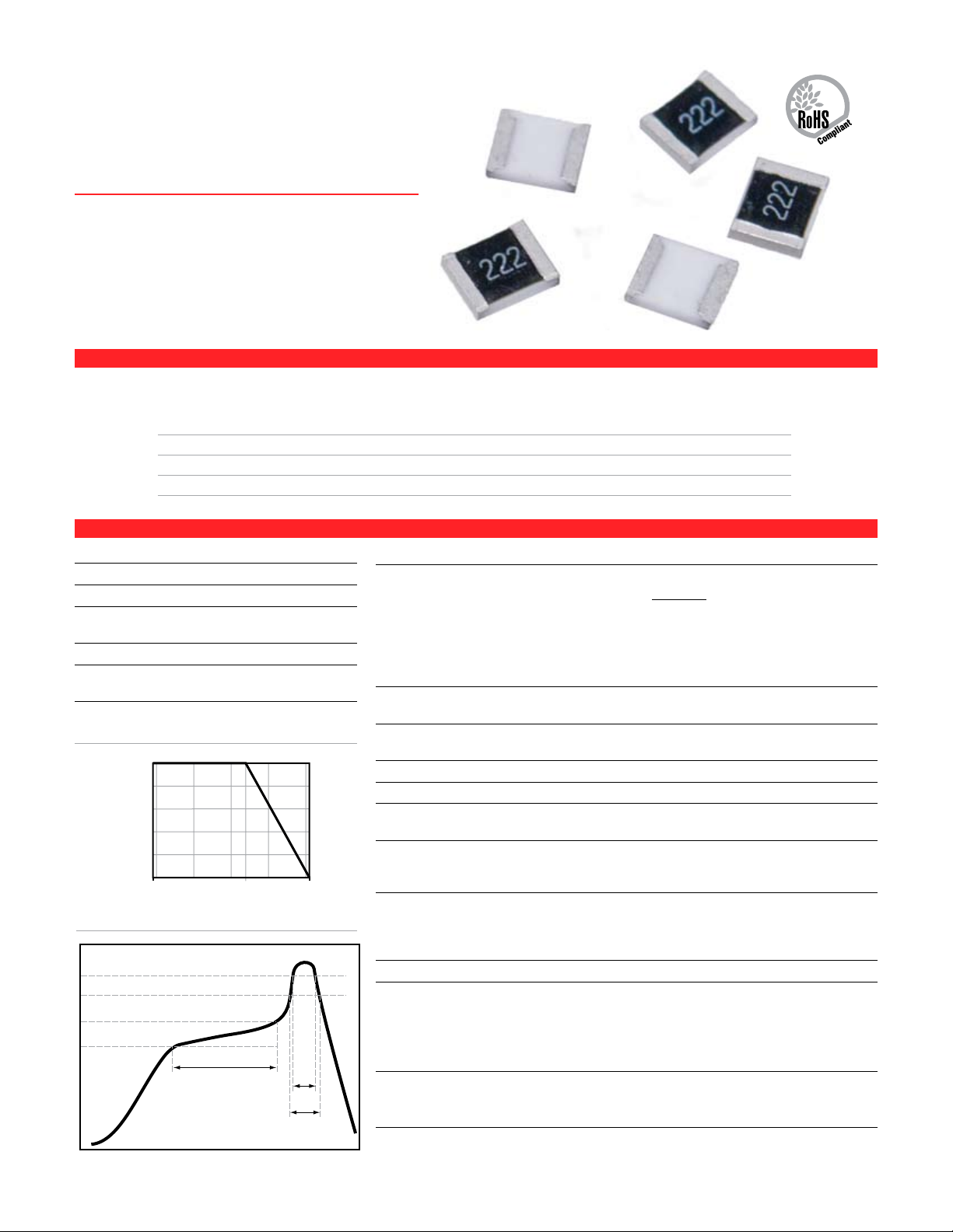
AS Series
Anti-surge Thick Film Chip Resistors
FEATURES
• Smallsizeandlightweight
• Suitableforbothwaveandreflowsoldering
• Canwithstandhighsurge
• Reductionofassemblycosts
SERIES SPECIFICATIONS
Power Max Max Dielectric
Rating Working Overload Withstanding Resistance
Type at 70°C Voltage Voltage Voltage Range
AS08 (0805) 0.33W 150V 300V 500V 1Ω~10MΩ
AS12 (1206) 0.5W 200V 400V 500V 1Ω~10MΩ
AS25 (2512) 1.5W 500V 500V 500V 1Ω~20MΩ
CHARACTERISTICS
-55°C ~ +155°C
E-24 values
Thick film
Silver, copper, nickel,
and tin, non-SAC alloy
Matte tin
±5% standard; ±10%
and ±20% available
Test ΔR Test Methods (JIS C 5201-1 )
Temperature
Soldering Heat
Temperature
withstanding
Derating
Reflow
6
Std. Oper. Temp.
Standard Values
Construction
Terminal material
Solderable finish
Tolerance
Coefficient
Short Time
Overload
Terminal
Bending
Single Pulse
Humidity
Load Life in
Humidity
Load Life
Solderability
Cycling
Dielectric
voltage
1Ω-10Ω: ≤ ±400PPM/°C
(±200 PPM can be provid-
ed on a case to case basis)
11Ω-10MΩ: ≤ ±100PPM/°C
±(1.0% + 0.1Ω) max. Permanent ΔR after the application of a
±(1.0% + 0.05Ω) max. Twist of Test Board: Y/X = 3/90 mm for
±(1.0% + 0.05Ω) max. 260°C±3°C for 10 ±1 sec.
±(1.0% + 0.1Ω) max. See graph on next page.
±(3.0% + 0.1Ω) max. Temporary ΔR after 240 hr. at 40 ±2°C
±(3.0% + 0.1Ω) max. ΔR after 1,000 hr. (1.5 hr. "on", 0.5 hr.
±(3.0% + 0.1Ω) max. ΔR change after 1,000 hr. operat-
Min. 95% coverage Wave Solder: 245°C ±3°C for 2-3 sec.
±(1.0% + 0.05Ω) max. ΔR after 5 cycles:
No evidence of flashover,
mechanical damage, arcing
or insulation breakdown
Natural ΔR/°C
R2-R1
R1(t2-t1)
R1: at room temp. (T1)
R2: at room temp. plus 100°C (T2)
Test pattern: room temp. (T1), room
temp. +100°C(T2)
potential of 2.5 times RCWV for 5 sec.
60 sec.
and 90-95% relative humidity
"off" ) at RCWV at 40 ±2°C and 90-95%
relative humidity
ing at RCWV, with duty cycle of (1.5
hours"on", 0.5 hour"off") at 70°C ±2°C
ambient
-55°C ±3°C 30 min.
Room temp. 10-15 min.
+155°C ±2°C 30 min.
4 Room temp. 10-15 min.
Clamped in the trough of a 90°C metal-
lic v-block at specified AC potential
60-70 sec.
x 106 (PPM/°C)
Page 2

AS Series
a a
b b
178 ±2
60 ±1
13 ±.5
2 ±.5
W ±1
21 ±.5
A ±.2
B ±.2
T ±.1
1.5 +0.1/-0
1.75 ±.1
3.5 ±0.05
4.0 ±.1
8.0 ±.2
Paper
Embossed
2.0 ±.05
A ±.2
B ±.2
1.0 ±.1
1.5 +0.1/-0
1.5 +0.1/-0
1.75 ±.1
3.5 ±0.05
4.0 ±.1
8.0 ±.2
2.0 ±.05
AS08J1004ET
RoHS
compliant
Ohms
First 3 digits are
significant; 4th digit
is multiplier. Values
below 100 ohms use
"R" as a decimal
holder.
examples:
1001 = 1000 ohms
1502 = 15000 ohms
Tolerance
J = 5%
standard
for E24
values
Series
AS08= 0805
AS12= 1206
AS25= 2512
TCR
T= tape and
reel: 0805 and
1206 paper
tape; 2512
embossed tape.
Single
AS25
AS12
AS08
AS25
AS12
AS08
Continuous (100KΩ)
AS25
AS12
AS08
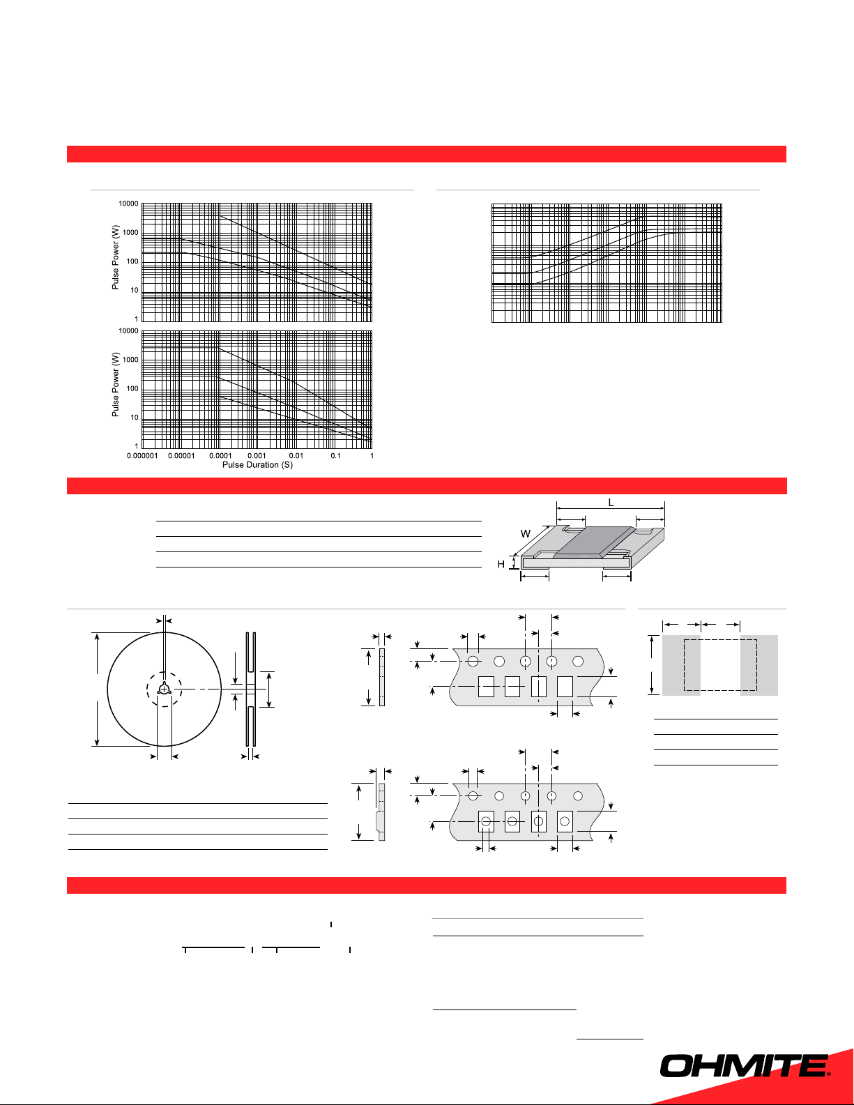
1.2/50µs Lightning Surge
Resistance (Ω)
Voltage (V)
10,000
1,000
100
10
1 10 100 1K 10K 1M100K
B C
A
Anti-surge Thick Film Chip Resistors
CHARACTERISTICS
Pulse Curve Lightning Surge
DIMENSIONS
(mm)
Series L W H a b
AS08 2.00 ±0.15 1.25 +0.15/-0.10 0.55 ±0.10 0.40 ±0.20 0.40 ±0.20
AS12 3.10 ±0.15 1.55 +0.15/-0.10 0.55 ±0.10 0.45 ±0.20 0.45 ±0.20
AS25 6.35 ±0.10 3.10 ±0.15 0.55 ±0.10 0.60 ±0.25 0.50 ±0.20
Tape and Reel Land Pattern
Series Packaging Qty./reel A B T W
AS08 Paper 5,000 pcs. 1.65 2.40 0.81 10
AS12 Paper 5,000 pcs. 2.00 3.60 0.81 10
AS25 Embossed 4,000 pcs. 3.50 6.70 1.0 13.8
rev 10/20-2
ORDERING INFORMATION
Standard Part Numbers
0805
AS08J1R00ET
AS08J10R0ET
AS08J1000ET
AS08J1001ET
AS08J1002ET
AS08J1003ET
AS08J1004ET
1206
AS12J1R00ET
AS12J10R0ET
AS12J1000ET
AS12J1001ET
AS12J1002ET
AS12J1003ET
AS12J1004ET
2512
AS25J1R00ET
AS25J10R0ET
AS25J12R0ET
AS25J15R0ET
AS25J22R0ET
AS25J1000ET
AS25J1001ET
AS25J1002ET
AS25J1003ET
AS25J1004ET
7
Series A B C
AS08 1.3 1.2 1.0
AS12 1.8 1.2 2.2
AS25 3.0 2.5 4.0
 Loading...