


IEEE 802.11 b/g/n
300Mbps W iFi Module
Product Specifications
Model: GWF-1M01
Version: 1.1
2012-11-20
Information in this document is subject to change without prior notice. Page
1 of 13
1. Introduction
The GWF-1M01 is a WLAN module supporting IEEE 802.11b/g/n standards with 7-pin or 4-pin connector
supporting USB2.0 interface. This is a small form factor and low cost compact WLAN module designed for
the wireless connectivity. This module operates in 2.4GHz ISM frequency band, it applies a highly integrated
MAC/BBP and RF single chip RT 5372 with 300Mbp s PHY rate supporting. It fully complies wit h IEEE802.11n
draft 3.0 and IEEE802.1 1b/g feature.
2. Features
z
20MHz/40MHz bandwidth support.
802.11b: 1, 2, 5.5, 11Mbps; 802.11g: 6, 9, 12, 24, 36, 48, 54Mbps ;
z
z
802.11n: Support PHY rate up to 300Mbps.
z
Security support for WEP 64/128, WPA,WPA2, TKIP,AES
3. Product Information
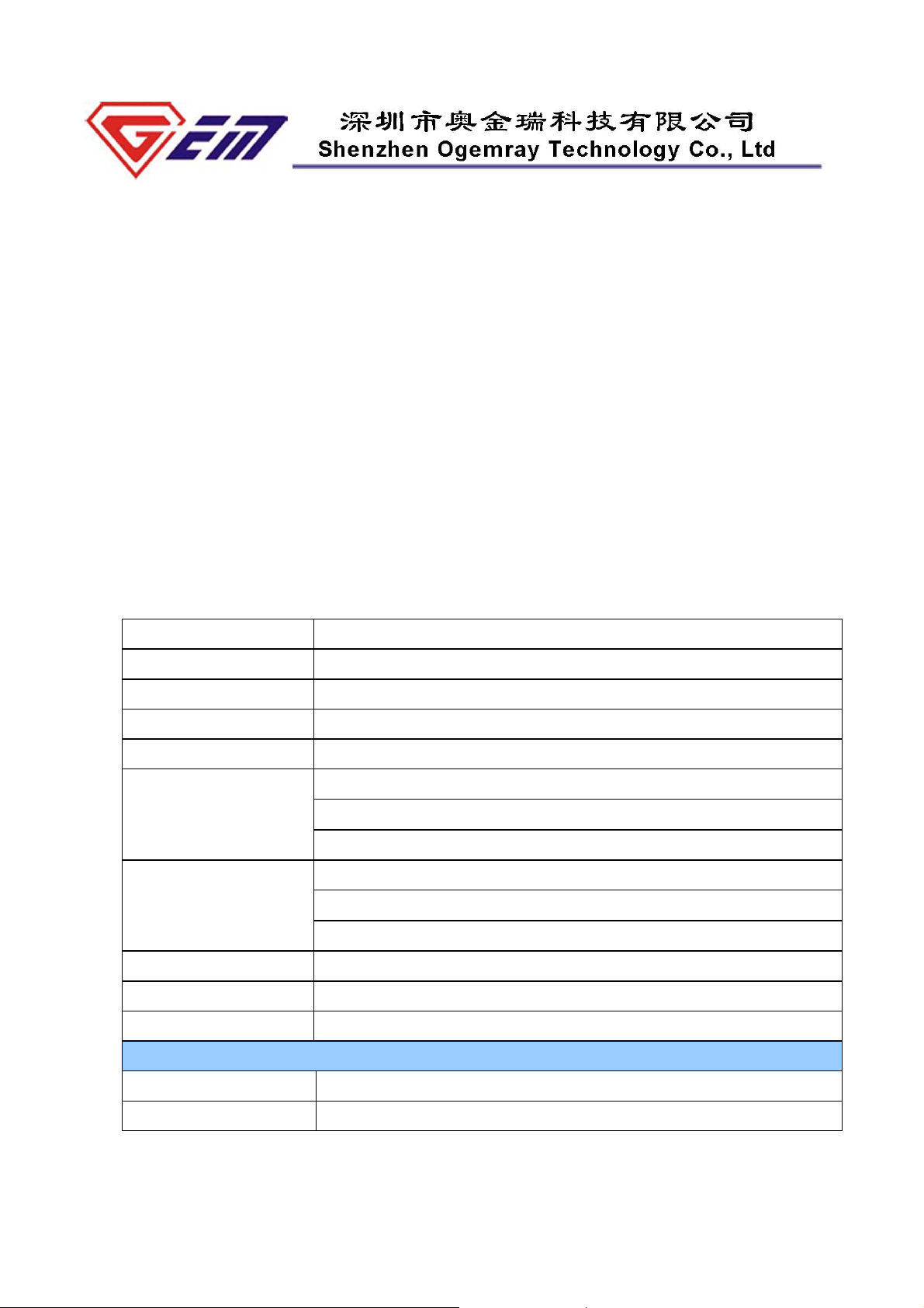
3.1 Specification:
Main Chipset Ralink RT5372
Operation Frequency 2412~2462MHz, ISM band
Protocols
802.11b: CCK, QPSK, BPSK, 802.11g/n: OFD M
Antennas Two outputs to external antennas
Security WPA/WPA2, 64/128/152-bit WEP , WPS
802.11b (CCK) : 20.5+/-1dBm
Typical Transmit Power
(Antenna feed point)
802.11g (OFDM) : 16.5+/-1dBm
802.11n (HT20@MCS7), 16+/-1dBm; (HT40@MCS7),16+/-1dBm
802.11b: -88+/-1dBm
Receive Sensitivity
(Antenna feed point)
802.11g: -73+/-1dBm
802.11n (HT20), -71+/-1dBm; 802.11n (HT40), -68+/-1dBm
Operating V ol tage
Bus Interface
Interface
5.0VDC ± 5% ; <300mA @802.11g ; or3.3VDV± 5%
USB 2.0
7-pin or 4-pin, 2.0mm , or 4-pin 2.54 mm pitch pin header
Physical Specification
Dimensions 33* 15*3 mm
Weight 1.6 g
Information in this document is subject to change without prior notice. Page
2 of 13
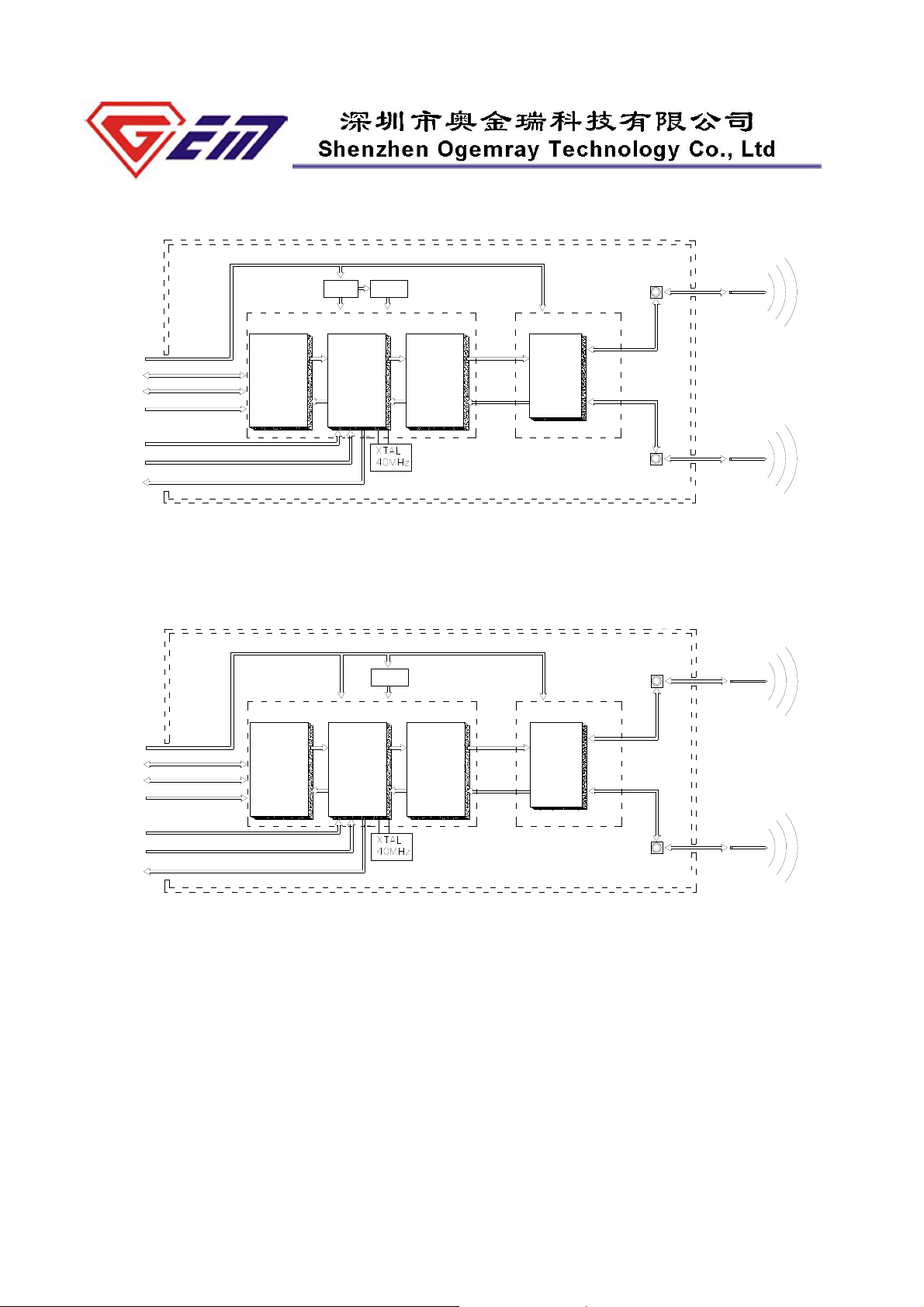
3.2 Block Diagram
VCC (5V)
USB
Connector
DATA-
DATA+
GND
TX CONTROL
WPS CONTROL
EXTERNAL LED
USB
Interface
5V/3.3V
RT5372
Baseband
Packet
Buffer/
Encrption
Engine
MAC/
3.3V/1.5V
RF
Transmitter
RF
Receiver
TX/RX
Front End
USB WiFi adapter
I-PEX
Receptacle
I-PEX
Receptacle
External antenna
2.412~2.462GHz
External antenna
2.412~2.462GHz
Figure 1: System Block Diagram of 7 pin GWF-1M01 5.0V WLAN Module
I-PEX
Receptacle
I-PEX
Receptacle
External antenna
2.412~2.462GHz
External antenna
2.412~2.462GHz
USB
Connector
VCC (5V)
DATA-
DATA+
GND
TX CONTROL
WPS CONTROL
EXTERNAL LED
USB
Interface
RT5372
Baseband
MAC/
Packet
Buffer/
Encrption
Engine
3.3V/1.5V
RF
Transmitter
RF
Receiver
TX/RX
Front End
USB WiFi adapter
Figure 2: System Block Diagram of 7 pin GWF-1M04 3.3V WLAN Module
Information in this document is subject to change without prior notice. Page
3 of 13
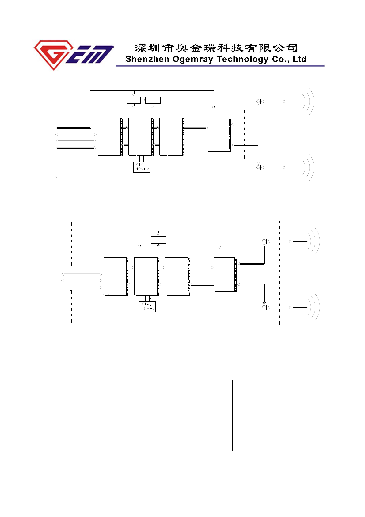
USB
Connector
VCC (5V)
DATA-
DATA+
GND
USB
Interface
5V/3.3V
RT5372
Baseband
MAC/
Packet
Buffer/
Encrption
Engine
3.3V/1.5V
RF
Transmitter
RF
Receiver
TX/RX
Front End
I-PEX
Receptacle
External antenna
2.412~2.462GHz
USB WiFi adapter
I-PEX
Receptacle
External antenna
2.412~2.462GHz
Figure 3: System Block Diagram of 4 pin GWF-1M04 5.0V WLAN Module
I-PEX
Receptacle
I-PEX
Receptacle
External antenna
2.412~2.462GHz
External antenna
2.412~2.462GHz
USB
Connector
VCC (5V)
DATA-
DATA+
GND
USB
Interface
RT5372
Baseband
MAC/
Packet
Buffer/
Encrption
Engine
3.3V/1.5V
RF
Transmitter
RF
Receiver
TX/RX
Front End
USB WiFi adapter
Figure 4: System Block Diagram of 4 pin GWF-1M04 3.3V WLAN Module
3.3 Software and system Information
Operation System
Linux 2.4/2.6
Windows XP/Vista/7
Windows CE 5.0/6.0
Mac OS X 10.4~10.7
CPU Supplier
ARM, MIPSII
X86 Platform
ARM, MIPSII
N/A
Driver
Available
Available
Available
Available
Information in this document is subject to change without prior notice. Page
4 of 13
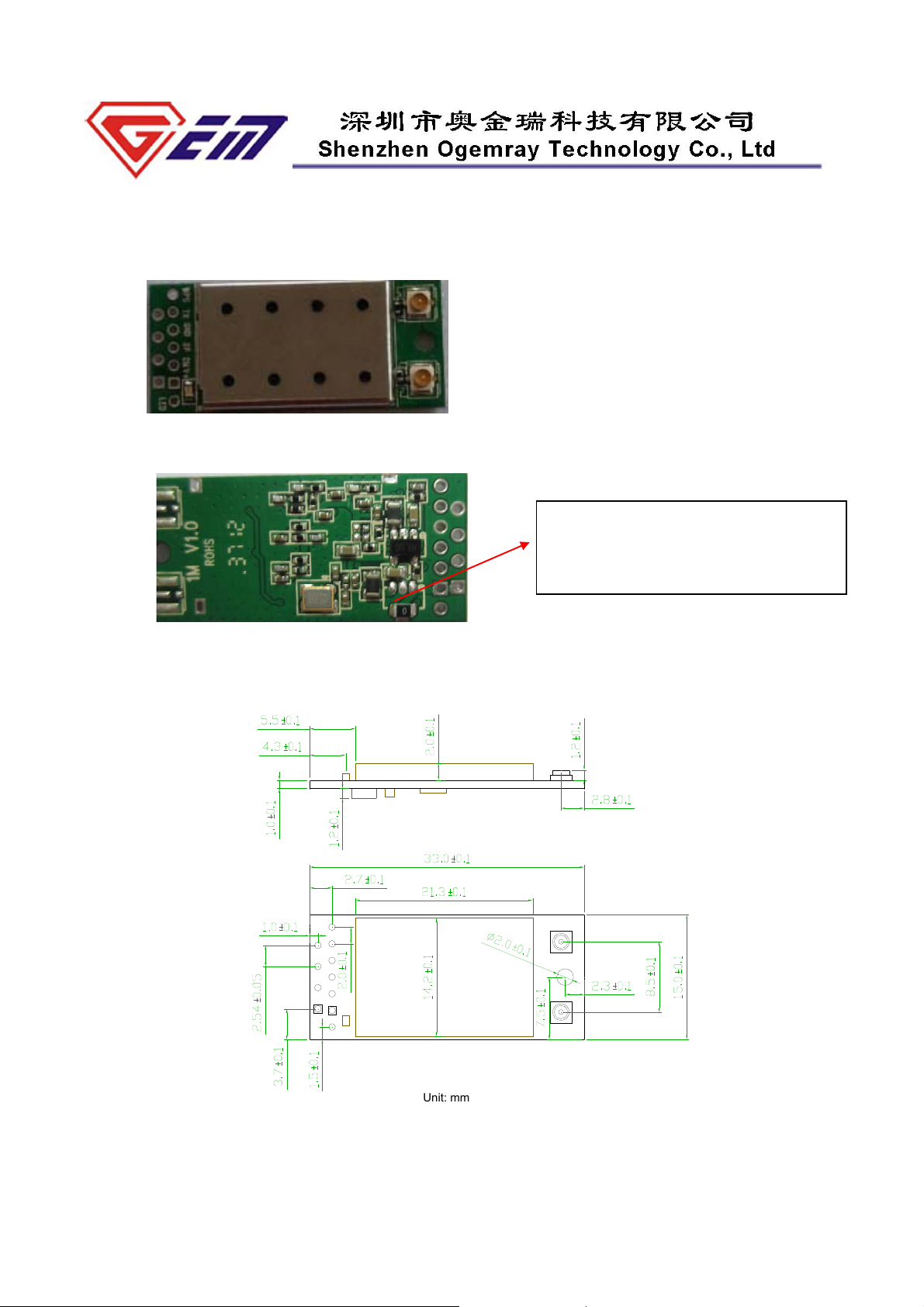
3.4 Mechanical Information
3.4.1 OUTLINE and Connection Interface (Pictures are for reference only)
Figure 5: 5.0VDC power input module.
For 3.3 VDC power input, the inductor is
removed and the DC/DC chipset is replace d
with a 0 ohm resistor
Figure 6: 3.3VDC power input module.
Unit: m
m
Figure 7: General dimensions
Information in this document is subject to change without prior notice. Page
5 of 13

3.4.1.1
4-pin 2.54 mm pitch pin header.
a). Model: GWF-1M01-50-T-2.54-4-1; GWF-1M01-33-T-2.54-4-1
R
F
Connector
LED
LED
Shield Case
Shield Case
Unit: m
m
Figure 8: Top side 4–Pin 2.54mm pitch pin header interface.
b). Model: GWF-1M01-50-B-2.54-4-1; GWF-1M01-33-B-2.54-4-1
R
F
LED
LED
Shield Case
Shield Case
Unit: m
m
Connector
Figure 9: Bottom side 4–Pin 2.54mm pitch pin header interface.
Information in this document is subject to change without prior notice. Page
6 of 13

3.4.1.2
4-pin 2.0 mm pitch pin header
a). Model: GWF-1M01-50-T-2.0-4-1; GWF-1M01-33-T-2.0-4-1
R
F
Connector
LED
LED
Shield Case
Shield Case
Unit: m
m
Figure 10: Top side 4–Pin 2.0mm pitch pin header interface.
b). Model: GWF-1M01-50-B-2.0-4-1; GWF-1M01-33-B-2.0-4-1
R
F
LED
LED
Shield Case
Shield Case
Unit: m
m
Connector
Figure 11: Bottom side 4–Pin 2.0mm pitch pin header interface.
Information in this document is subject to change without prior notice. Page
7 of 13

3.4.1.3
7-pin 2.0 mm pitch pin header
a). Model: GWF-1M01-50-T-2.0-7-1; GWF-1M01-33-T-2.0-7-1
LED
Shield Case
Shield Case
LED
R
F
Connector
Figure 12: Top side RF connector & 7–Pin 2.0mm pitch pin header interface.
b). Model: GWF-1M01-50-T-2.0-7-2; GWF-1M01-33-T-2.0-7-2
LED
Shield Case
R
F
Connector
Shield Case
LED
Unit: m
m
Figure 13: Bottom side RF connector & top side 7–Pin 2.0mm pitch pin header interface.
Information in this document is subject to change without prior notice. Page
8 of 13

c). Model: GWF-1M01-50-B-2.0-7-1; GWF-1M01-33-B-2.0-7-1
R
F
LED
LED
Shield Case
Shield Case
Unit: m
m
Connector
Figure 14: Top side RF connector & Bottom side 7–Pin 2.0mm pitch pin header interface.
d). Model: GWF-1M01-50-B-2.0-7-2; GWF-1M01-33-B-2.0-7-2
LED
Shield Case
R
F
Connector
Shield Case
LED
Unit: m
m
Figure 15: Bottom side RF connector & 7–Pin 2.0mm pitch pin header interface.
Information in this document is subject to change without prior notice. Page
9 of 13

e). Model: GWF-1M01-50-F-2.0-7-1; GWF-1M01-33-F-2.0-7-1
R
F
LED
LED
Shield Case
Shield Case
Unit: m
m
Connector
Figure 16: Bottom side 7–Pin 2.0mm pitch 90 degree pin header interface.
3.4.2 Pin definition:
Pin-out 7-pin 2.0mm pitch pin header 4-pin 2.0 or 2.54mm pitch pin header
1 WPS control
2
3
4
5
6
7
RF/TX ON/OFF control DP (USB data+)
GND (Ground) DM (USB data-)
DP (USB data+) VCC (3.3 VDC or 5.0VDC)
DM (USB data-) N/A
VCC (3.3 VDC or 5.0VDC) N/A
LED* (Wireless TX status) N/A
3.4.3 RF output Connection Information
GND (Ground)
If the I-PEX RF connection is selected, a 50 ohm external antenna connects to the module
RF output via an I-PEX MHF receptacle (RF connector). ( Part No: 20279-001E-01).
Information in this document is subject to change without prior notice. Page
10 of 13

The profile of the I-PEX connector
Note: the MHF receptacle can be mounted at the top side or bottom side of the PCB.
RF Output Type:
Type 1-2
RF Receptacle
RF Receptacle
RF output via
MHF Receptacle
RF Cable be directly
soldered on board
Type 3
Antenna
Antenna
Information in this document is subject to change without prior notice. Page
11 of 13

3.4.4 Ordering information
Since there are many different types of pin header might be used, such as: straight pin; 90 degree
bend pin; long pin; short pin…, please mention the detail requirement of the pin header when
ordering. It can be mentioned by part number or by descriptions.
4 Agency Approval
Agency
FCC Part15
CE
RoHS
Approval
Pre-scan undergoing
Pre-scan undergoing
√
Information in this document is subject to change without prior notice. Page
12 of 13

5 Environment
5.1 Temperature
5.1.1 Operating Temperature
Continuous reliable operation in ambient temperature: -10ºC to +60ºC.
5.1.2 Storage Temperature
The product is not damaged or degraded when keeping in -20ºC to +85ºC.
5.2 Humidity
5.2.1 Operating Humidity Condition s
The product should be capable of continuous reliable operation when subjected to relative humidity in
the range of 20% to 80% (non-condensing) .
5.2.2 Non-Operating Humidity Conditions (including warehouse)
The product should not be damaged or degraded when kept in the place (where relative humidity
range is in the range of 20% to 80%) for 36 hours.
6 Disclaimer
THESE MATERIALS AND INFORMATION ARE PROVIDED “AS IS” WITHOUT WARRANTY OF ANY
KIND, EITHER EXPRESS OR IMPLIED , INCLUDING BUT NOT LIMITED TO, THE IMPLIED
WARRANTIES OF MERCHANTABILITY, FITNESS FOR A PARTICU LAR PURPOSE OR
NON-INFRINGEMENT.
We uses reasonable efforts to include accurate and up-to-date information on this document; it does not,
however, make any representations as to its accuracy or completeness of the information, text, graphics,
links or other items contained within these materials. Your use of this Document is at your own risk. Ogemray,
its suppliers, and other parties involved in creating and delivering this Document’s contents shall not be liable
for any special, indirect, incidental, or consequential damages, including without limitation, lost revenues or
lost profits.
Information in this document is subject to change without prior notice. Page
13 of 13

FCC Statement
1. This device complies with Part 15 of the FCC Rules. Operation is subject to the following two conditions:
(1) This device may not cause harmful interference.
(2) This device must accept any interference received, including interference that may cause undesired operation.
2. Changes or modifications not expressly approved by the party responsible for compliance could void the user's
authority to operate the equipment.
NOTE:
This equipment has been tested and found to comply with the limits for a Class B digital device, pursuant to Part 15 of
the FCC Rules. These limits are designed to provide reasonable protection against harmful interference in a residential
installation.
This equipment generates uses and can radiate radio frequency energy and, if not installed and used in accordance with
the instructions, may cause harmful interference to radio communications. However, there is no guarantee that
interference will not occur in a particular installation. If this equipment does cause harmful interference to radio or
television reception, which can be determined by turning the equipment off and on, the user is encouraged to try to
correct the interference by one or more of the following measures:
Reorient or relocate the receiving antenna.
Increase the separation between the equipment and receiver.
Connect the equipment into an outlet on a circuit different from that to which the receiver is connected.
Consult the dealer or an experienced radio/TV technician for help.
This module must be installed and operated in accordance with provided instructions and the antenna used for this
transmitter must be installed to provied a separation distance of at least 20 cm from all persons and must not be
co-located or operating in conjunction with any other antenna or transmitter. End-uses and installers must be
provide with antenna installation instructions and transmitter operating conditions for satisfying RF exposure
compliance.
Host device of OEM integrator must be labeled with: CONTAINS TX FCC ID: YWTWF53721MX
 Loading...