

.
SPECIFICATION FOR APPROVAL
Version:
1.0
Client
Product
WiFi Module
Descriptions IEEE 802.11n, 1T1R, 150Mbps
Vendor P/ N.
Issued By Gordon
Checked By
Confirmed By
GWF-3B
Gordon
Date
Date
Date
2015/02/28
2015/03/09
Pro
du
ct Sp
e
cific
ation
s
Version:
150Mbps 802.11
Single side WiFi
Model:
Date:
2015/02/26
1.0
GWF-3B
b/g/n
Module
1. Introduction
GWF-3B is a WLAN module supporting IEEE 802.11 b/g/n standards with 6-pin connector
supporting USB 2.0 /1.1 interface. This is a small form factor and low cost compact WLAN
module designed for the wireless connectivity of products with embedded system.
This module operates in 2.4GHz ISM frequency band, it applies a highly integrated MAC/BBP
and RF single chip RT5370 with 150Mbps PHY rate supporting. This module can be
other
embedded applications such as IP Camera, IP set top box, GPS, Internet radio apparatus,
it can be directly soldered on a main PCB.
1.1 Features
802.11b: 1, 2, 5.5, 11Mbps; 802.11g: 6, 9, 12, 24, 36, 48, 54Mbps
802.11n: (20MHz) MCS0-7, Support up to 72Mbps
(40MHz) MCS0-7, Support up to 150Mbps
OFDM, Peak rate 150Mbps, Peak throughput 90Mbps.
Security support for 64/128 WEP, WPA, WPA2, TKIP, AES
Operates in 2.4GHz frequency bands. Power Management
WPS and TX external control, WiFi direct supported.
2. Product Information
2.1 Typical Specification Overview
Standards
IEEE802.11b/g/n (1T1R mode)
built-in
Operating Frequency 2.412GHz ~ 2.4835GHz,Details depend on different country region.
Protocols
Antenna
Security
Transmit Output Power
(Typical value to antenna)
Receive Sensitivity
(Typical value without
antenna)
Operating Voltage
Operating Current(OFDM,
54Mbps)
802.11b: CCK, QPSK, BPSK, 802.11g/n: OFDM
PCB Antenna
WPA/WP2/WPAI, 64/128/152-bit WEP, WPS
11b: 17±1.0dBm @ 11Mbps; 11g: 14±1dBm @ 54Mbps
802.11n: (HT20), 12+/-1dBm, 802.11n: (HT40), 12+/-1dBm
11b: -84dBm @ 11Mbps; 11g: -72dBm @ 54Mpbs.
802.11n: (HT20), -68dBm@MSC7, (HT40),-67dBm@MSC7
5.0V or 3.3VDV± 5%
5.0V power input,<160mA; 3.3V power input.<250mA;Tx off.<30mA
USB Interface
USB 2.0/1.1
Bus Interface
Max: 7 pins, 2.0 mm pitch pin header. Or Max: 7 pins semi-hole.
2.2 Hardware Information
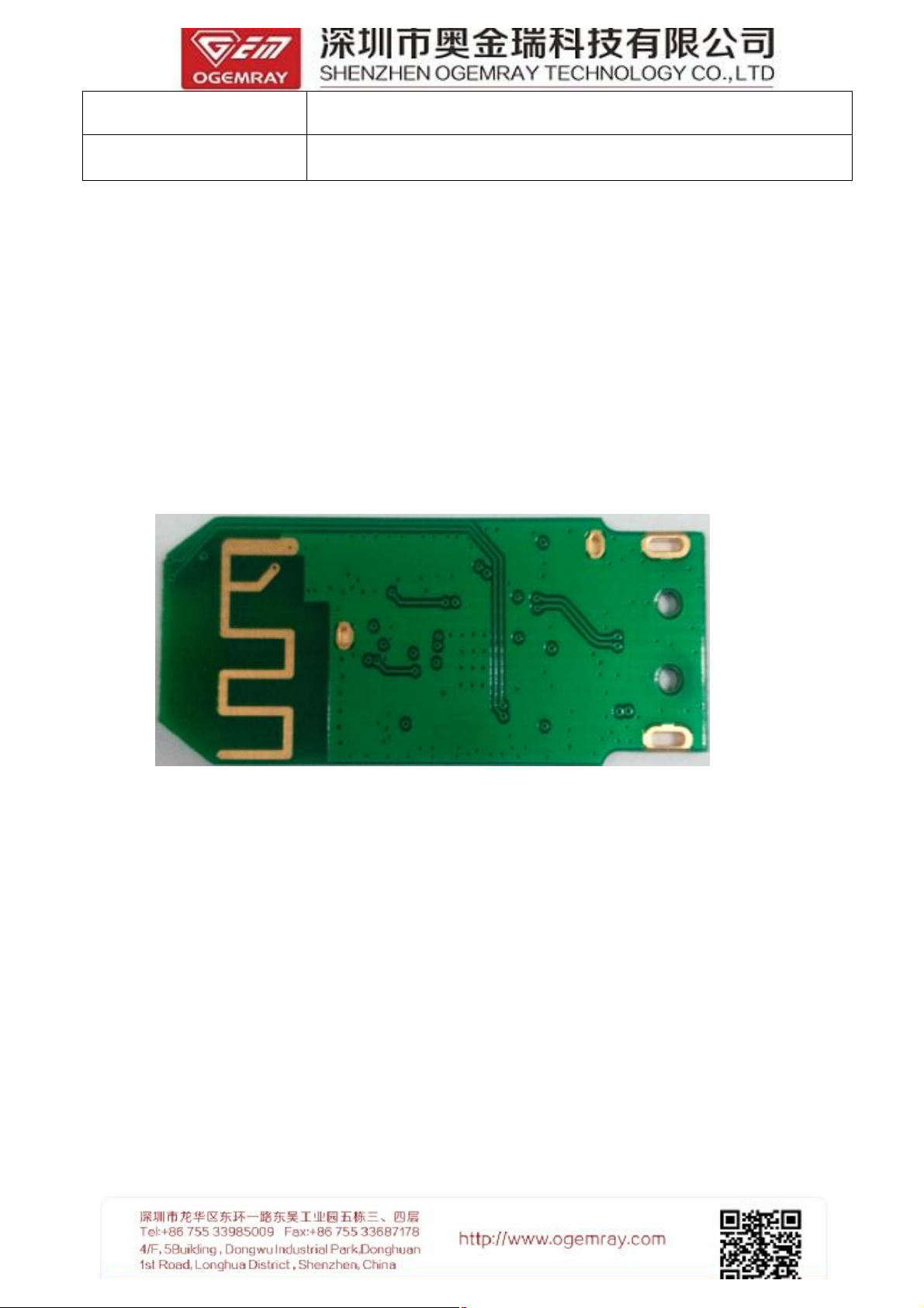
2.2.1 General view
Fig1. 3B Top pcb & Bottom pcb view

2.2.2 Block Diagram
USB
Interface
Fig 2.
5V DC 4pin power input with onboard PCB antenna used
VCC(5.0V)
DATADATA+
GND
TX CONTROL
EXTERNAL LED
CONTROL
WPS
USB
Interface
5V/3.3V 3.3V/1.5V
RT5370
Baseband
Encrption
MAC/
Packet
Buffer/
Engine
Transmitter
Receiver
RF
RF
RF
Front
End
2.412~2.4835GHz
USB WiFi
Module

2.2.3 Mechanical
A. Physical
Unit: mm
Information
Dimensions:
Fig 4. Pcb size

GND
UD+
UD-
VCC
b. USB 4 pin name schematic diagram
Fig
C. Pin Descriptions:
Pin Name
1
VCC 5.0V DC +/-5%
2
3
4
GND
5.
USB 4 pin name schematic diagram
Descriptions
UD-
USB
UD+ USB
Ground
data-
data+

b. on-board PCB antenna.
15.
Fig
’
16.
Fig
Peak gain: -1dBi, Average gain: -3dBi

Figure 18: A recommended antenna (Airgain P/N:N2420) and its radiation pattern
2.3 Software and system Information
Operation System CPU Supplier Driver
Linux 2.4/2.6 ARM, MIPSII Available
Windows XP/Vista/7/8 X86 Platform Available
Windows CE 5.0/6.0 ARM, MIPSII Available
Mac OS X 10.3~10.8 N/A Available
Android 4.1 N/A Available
Notes: The chipset manufacturer has initiated different kind of software, please describe
detail requirements for better selection.

2.4. Design
Concerns:
2.4.1 Power supply:
1) The input power can be 5.0V DC , please mentioned it when place an order.
2) The external power shall be well designed with enough capacity.
2.4.2 Using semi-holes:
1) When the module is designed to be soldered on a main PCB board directly,
the area under the antenna end of the module should be keep clear of metallic
components, connectors, vias, traces and other materials that can interfere with the
radio signal. The recommended clear space requirements are refer to Fig 12 and Fig
13.
2) The module is not recommended using reflow oven process, hand soldering
is suggested.
2.4.3 Clear place to use the module:
The following drawing shows a recommended footprint which can be a reference for a
main PCB design.
The clear space requirement for onboard antenna is suit for either pin header or
semi-holes connection application.
3. Certificates and Approval
Certificate Descriptions
FCC Part15 Available
CE Available
IC Available
KCC Approved by customers
RoHS Available

4. Environment
4.1 Temperature
4.1.1 Operating Temperature
Continuous reliable operation in ambient temperature: -10ºC to +60ºC.
4.1.2 Storage Temperature
The product is not damaged or degraded when keeping in -20ºC to +85ºC.
4.2 Humidity
4.2.1 Operating Humidity Conditions
The product should be capable of continuous reliable operation when subjected to relative
humidity in the range of 20% to 80% (non-condensing) .
4.2.2 Non-Operating Humidity Conditions (including warehouse)
The product should not be damaged or degraded when kept in the place (where relative
humidity range is in the range of 20% to 80%) for 48 hours.
5. Disclaimer
THESE MATERIALS AND INFORMATION ARE PROVIDED “AS IS” WITHOUT
WARRANTY OF ANY KIND, EITHER EXPRESS OR IMPLIED , INCLUDING BUT NOT
LIMITED TO, THE IMPLIED WARRANTIES OF MERCHANTABILITY, FITNESS FOR A
PARTICULAR PURPOSE OR NON-INFRINGEMENT.
We uses reasonable efforts to include accurate and up-to-date information on this document;
it does not, however, make any representations as to its accuracy or completeness of the
information, text, graphics, links or other items contained within these materials. Your use of
this Document is at your own risk. Ogemray, its suppliers, and other parties involved in creating
and delivering this Document’s contents shall not be liable for any special, indirect, incidental,
or consequential damages, including without limitation, lost revenues or lost profits.

FCC STATEMENT :
This device complies with Part 15 of the FCC Rules. Operation is subject to the following
two conditions:
(1) This device may not cause harmful interference, and
(2) This device must accept any interference received, including interference that may
cause undesired operation.
Warning: Changes or modifications not expressly approved by the party responsible for
compliance could void the user's authority to operate the equipment.
NOTE: This equipment has been tested and found to comply with the limits for a Class B
digital device, pursuant to Part 15 of the FCC Rules. These limits are designed to provide
reasonable protection against harmful interference in a residential installation. This
equipment generates uses and can radiate radio frequency energy and, if not installed
and used in accordance with the instructions, may cause harmful interference to radio
communications. However, there is no guarantee that interference will not occur in a
particular installation. If this equipment does cause harmful interference to radio or
television reception, which can be determined by turning the equipment off and on, the
user is encouraged to try to correct the interference by one or more of the following
measures:
Reorient or relocate the receiving antenna.
Increase the separation between the equipment and receiver.
Connect the equipment into an outlet on a circuit different from that to which the
receiver is connected.
Consult the dealer or an experienced radio/TV technician for help.

FCC INFORMATION (additional)
OEM INTEGRATION INSTRUCTIONS:
This device is intended only for OEM integrators under the following conditions: The module must
be installed in the host equipment such that 20 cm is maintained between the antenna and users,
and the transmitter module may not be co-located with any other transmitter or antenna. The
module shall be only used with the internal antenna(s) that has been originally tested and certified
with this module. As long as 3 conditions above are met, further transmitter test will not be
required. However, the OEM integrator is still responsible for testing their end-product for any
additional compliance requirements required with this module installed (for example, digital
device emissions, PC peripheral requirements, etc.).
Validity of using the module certification:
In the event that these conditions cannot be met (for example certain laptop configurations or
co-location with another transmitter), then the FCC authorization for this module in combination
with the host equipment is no longer considered valid and the FCC ID of the module cannot be
used on the final product. In these circumstances, the OEM integrator will be responsible for
re-evaluating the end product (including the transmitter) and obtaining a separate FCC
authorization.
End product labeling:
The final end product must be labeled in a visible area with the following: “Contains FCC ID:
YWT-GWF-3B”.
Information that must be placed in the end user manual:
The OEM integrator has to be aware not to provide information to the end user regarding how to
install or remove this RF module in the user's manual of the end product which integrates this
module. The end user manual shall include all required regulatory information/warning as show in
this manual.
Antenna Specification:
Type: PCB Antenna
Model: GWF-3B
Gain: 3.88 dBi
 Loading...