OEM 17MB15 Service Manual

42” PLASMA TV
17MB15-5
SERVICE MANUAL
i

TABLE OF CONTENTS
MAIN :
1. PRECAUTION.....................................................................................................................................................1
2. SERVICE MENU ITEMS.....................................................................................................................................1
2.1. SOUND 1..........................................................................................................................................................1
2.2. SOUND 2..........................................................................................................................................................1
2.3. Options.............................................................................................................................................................2
2.4. Features...........................................................................................................................................................2
2.5. Teletext.............................................................................................................................................................3
2.6. Tuner Options...................................................................................................................................................3
3. SOFTWARE UPDATE DESCRIPTION ..............................................................................................................4
3.1. ANALOG SOFTWARE UPDATE via SCART ..................................................................................................4
3.2. ANALOG SOFTWARE UPDATE via I2C..........................................................................................................5
3.3. EEPROM UPDATE via SCART .......................................................................................................................6
4. INTRODUCTION.................................................................................................................................................7
5. TUNER................................................................................................................................................................7
6. IF PART (TDA9886)............................................................................................................................................7
7. MULTI STANDARD SOUND PROCESSOR ......................................................................................................8
8. VIDEO SWITCH TEA6415..................................................................................................................................8
9. AUDIO AMPLIFIER STAGE WITH TPA3004D2 ................................................................................................8
10. POWER SUPPLY (SMPS)..................................................................................................................................9
11. MICROCONTROLLER .......................................................................................................................................9
12. SERIAL ACCESS CMOS 4Kx8(32KBit)EEPROM 24C32A...............................................................................9
13. CLASS AB STEREO HEADPHONE DRIVER TDA1308....................................................................................9
14. SAW FILTERS....................................................................................................................................................9
15. IC DESCRIPTIONS ..........................................................................................................................................10
15.1. 24LC02 .......................................................................................................................................................12
15.1.1. Description .........................................................................................................................................12
15.1.2. Features..............................................................................................................................................12
15.1.3. Pinning................................................................................................................................................12
15.2. 24C32.........................................................................................................................................................13
15.2.1. General Description ..........................................................................................................................13
15.2.2. Features..............................................................................................................................................13
15.2.3. Pinning................................................................................................................................................13
15.2.4. PIN Function Table ............................................................................................................................14
15.3. 74LVC14A...................................................................................................................................................14
15.3.1. Description .........................................................................................................................................14
15.3.2. Features..............................................................................................................................................14
15.3.3. Pinning................................................................................................................................................14
15.4. TEA6420.....................................................................................................................................................15
15.4.1. Features..............................................................................................................................................15
15.4.2. Description .........................................................................................................................................15
15.4.3. Pin Connections ................................................................................................................................15
15.5. CS4334.......................................................................................................................................................15
15.5.1. Features..............................................................................................................................................15
15.5.2. General Description ..........................................................................................................................16
15.5.3. Pin Descriptions ................................................................................................................................16
15.6. GAL16LV8 ..................................................................................................................................................16
15.6.1. Description .........................................................................................................................................16
15.6.2. Features..............................................................................................................................................16
15.6.3. Pin connections.................................................................................................................................17
15.7. ..........................................................................................................................................................................17
15.8. K6R4008V1D..............................................................................................................................................17
15.8.1. Description .........................................................................................................................................17
15.8.2. Features..............................................................................................................................................17
15.8.3. Pin Description ..................................................................................................................................18
15.9. KA278R33...................................................................................................................................................18
15.9.1. Features..............................................................................................................................................18
ii

15.9.2. Description .........................................................................................................................................18
15.10. LM1117.......................................................................................................................................................19
15.10.1. General Description ..........................................................................................................................19
15.10.2. Features..............................................................................................................................................19
15.10.3. Applications.......................................................................................................................................19
15.11. LM317.........................................................................................................................................................19
15.11.1. General Description ..........................................................................................................................19
15.11.2. Features..............................................................................................................................................19
15.11.3. Pin Description ..................................................................................................................................20
15.12. LM809.........................................................................................................................................................20
15.12.1. General Description ..........................................................................................................................20
15.12.2. Features..............................................................................................................................................20
15.12.3. Pinning................................................................................................................................................20
15.13. MSP34X1G (MSP3411G)...........................................................................................................................20
15.13.1. Introduction........................................................................................................................................21
15.13.2. Features..............................................................................................................................................21
15.14. M29W040B.................................................................................................................................................23
15.14.1. Description.........................................................................................................................................23
15.14.2. Features..............................................................................................................................................23
15.14.3. Pin Descriptions ................................................................................................................................24
15.15. MC33202....................................................................................................................................................24
15.15.1. General Description ..........................................................................................................................24
15.15.2. Features..............................................................................................................................................24
15.15.3. Pin Connections ................................................................................................................................25
15.16. PCF8574.....................................................................................................................................................25
15.16.1. General Description ..........................................................................................................................25
15.16.2. Features..............................................................................................................................................25
15.16.3. Pinning................................................................................................................................................25
15.17. TSOP1836..................................................................................................................................................26
15.17.1. Description.........................................................................................................................................26
15.17.2. Features..............................................................................................................................................26
15.18. PI5V330......................................................................................................................................................26
15.18.1. General Description ..........................................................................................................................26
15.19. SDA55XX (SDA5550).................................................................................................................................27
15.19.1. General description...........................................................................................................................27
15.20. Sil 9993.......................................................................................................................................................27
15.20.1. General Description ..........................................................................................................................27
15.20.2. Features..............................................................................................................................................27
15.21. SN74CB3Q3305.........................................................................................................................................28
15.21.1. General Description ..........................................................................................................................28
15.21.2. Features..............................................................................................................................................28
15.21.3. Pin Connections ................................................................................................................................28
15.22. ST24LC21...................................................................................................................................................28
15.22.1. Description.........................................................................................................................................28
15.22.2. Features..............................................................................................................................................29
15.22.3. Pin connections.................................................................................................................................29
15.23. LM2576.......................................................................................................................................................29
15.23.1. General Description ..........................................................................................................................29
15.23.2. Features..............................................................................................................................................29
15.23.3. Pin description...................................................................................................................................30
15.24. MC34063....................................................................................................................................................30
15.24.1. Description.........................................................................................................................................30
15.24.2. Features..............................................................................................................................................30
15.24.3. Pin connections.................................................................................................................................30
15.25. TDA1308.....................................................................................................................................................31
15.25.1. General Description ..........................................................................................................................31
15.25.2. Features..............................................................................................................................................31
15.25.3. Pinning................................................................................................................................................31
15.26. TDA9886.....................................................................................................................................................31
15.26.1. General Description ..........................................................................................................................31
iii

15.26.2. Features..............................................................................................................................................31
15.26.3. Pinning................................................................................................................................................32
15.27. TPA3004D2................................................................................................................................................32
15.27.1. General Description ..........................................................................................................................32
15.27.2. Features..............................................................................................................................................32
15.27.3. Pinning................................................................................................................................................33
15.28. ........................................................................................................................................................................34
15.29. µPA672T.....................................................................................................................................................34
15.29.1. General Description ..........................................................................................................................34
15.29.2. Features..............................................................................................................................................35
15.29.3. Pin Connection ..................................................................................................................................35
15.30. VPC3230D..................................................................................................................................................35
15.30.1. General Description ..........................................................................................................................35
15.30.2. Pin Connections and Short Descriptions .......................................................................................35
15.31. SVP-EX 52B...............................................................................................................................................37
16. SERVICE MENU SETTINGS............................................................................................................................37
16.1. Picture Adjust..............................................................................................................................................37
16.2. SOUND1.....................................................................................................................................................37
16.3. SOUND 2....................................................................................................................................................37
16.4. Options........................................................................................................................................................38
17. IC DESCRIPTIONS (FOR DIGITAL) ................................................................................................................39
17.1. STI5518 ......................................................................................................................................................39
17.1.1. General Description ..........................................................................................................................39
17.2. MAX232_SMD............................................................................................................................................39
17.2.1. General Description ..........................................................................................................................39
17.2.2. Features..............................................................................................................................................39
17.3. 74HCU04....................................................................................................................................................39
17.3.1. General Description ..........................................................................................................................39
17.3.2. Pin Description ..................................................................................................................................39
17.4. TSH22.........................................................................................................................................................40
17.4.1. General Description ..........................................................................................................................40
17.4.2. Pin Connections ................................................................................................................................40
17.5. CS4334.......................................................................................................................................................41
17.5.1. General Description ..........................................................................................................................41
17.5.2. Features..............................................................................................................................................41
17.6. AMIC A43L2616 .........................................................................................................................................41
17.6.1. General Description ..........................................................................................................................41
17.6.2. Features..............................................................................................................................................41
17.6.3. Pin Description ..................................................................................................................................42
17.7. MX29LV160T..............................................................................................................................................43
17.7.1. General Description ..........................................................................................................................43
17.7.2. Features..............................................................................................................................................44
17.7.3. Pin Description ..................................................................................................................................44
17.8. 24C32.........................................................................................................................................................44
17.8.1. General Description ..........................................................................................................................44
17.8.2. Features..............................................................................................................................................45
17.8.3. Pin Description ..................................................................................................................................45
17.9. STV0360.....................................................................................................................................................45
17.9.1. General Description ..........................................................................................................................45
17.9.2. Features..............................................................................................................................................46
17.9.3. Pin Description ..................................................................................................................................46
17.10. MAX809......................................................................................................................................................48
17.10.1. General Description ..........................................................................................................................48
17.10.2. Features..............................................................................................................................................49
17.10.3. Pin Description ..................................................................................................................................49
17.11. TDCC2345TV39A.......................................................................................................................................49
17.11.1. General Description ..........................................................................................................................49
17.11.2. Pin Description ..................................................................................................................................50
17.12. STV0700.....................................................................................................................................................50
17.12.1. General description...........................................................................................................................50
iv

17.12.2. Features..............................................................................................................................................50
17.12.3. Pin Description ..................................................................................................................................51
18. APPENDIX A
18.1. EXPLODED VIEW AND PART LIST...............................................................................................................53
19. APPENDIX B......................................................................................................................................................54
19.1. BLOCK DIAGRAMS ..................................................................................................................................55
19.2. 16.ELECTRICALDIAGRAMS ......................................................................................................................56
19.2.1. POWER BOARD..................................................................................................................................57
19.2.2. MAIN BOARD ..............................................................................................................................58
19.2.3. APLIFIER BOARD..................................................................................................................................59
19.2.4. 17FAV15-2 BOARD...............................................................................................................................60
19.3. WIRING DIAGRAM..............................................................................................................................71
19.4. PRINT_LAY-OUTS ..............................................................................................................................72
19.4.1. 1Complete_PCB_Pattern_Schematic..................................................................................................73
19.4.2. Top_Level_PCB_Pattern.................................................................................................................74
19.4.3. In-1_Ground_Level_PCB_Pattern.....................................................................................................75
19.4.4. In2_Power_Level_PCB_Patter ......................................................................................................... 76
19.4.5. Bottom_ Level_ PCB_ Pattern...........................................................................................................77
19.4.6. Top_Layer_Silk_Print..........................................................................................................................78
19.4.7. Bottom_Layer_Silk_Print....................................................................................................................79
19.4.8. Topmask.lgx........................................................................................................................................80
19.4.9. Bottommsk.lgx...................................................................................................................................81
19.4.10. 17fav15-2pcb.......................................................................................................................................82
19.4.11. 18amp05-2 pcb.................................................................................................................................. ..83
20. APPENDIX C ....................................................................................................................................................83
20.1. SPARE PART LIST ............................................................................................................................ ..........84
......................................................................................................................................................52
v

1. PRECAUTION
2. SERVICE MENU ITEMS
2.1. SOUND 1
a) Menu Subwoofer => If ON, Subwoofer option is available in TV set, and the item is
visible in sound menu, else Subwoofer is not available. Default “ON”.
b) Subwoofer Level (dB) => This value is gain value of Subwoofer output in dB.
-30...12. Default “0” dB.
c) Subwoofer Corner Freq. (x10Hz) => Last low frequency value that is amplified. 5...40.
Default “22” x 10Hz = 220Hz.
d) Menu Equalizer => If ON, visible in sound menu, else invisible. Default “ON”.
e) Menu Headphone => If ON, visible in sound menu, else invisible. Default “ON”.
f) Menu Effect => If ON, visible in sound menu, else invisible. Default “ON”.
g) Menu Wide Sound => If ON, visible in sound menu, else invisible. Default “OFF”.
h) Menu Dynamic Bass => If ON, visible in sound menu, else invisible. Default “ON”.
i) Menu Virtual Dolby => If ON, visible in sound menu, else invisible. Default “ON”.
j) Carrier Mute => If ON, in the absence of an FM carrier the output is muted, else not.
Default “ON”.
k) Virtual Dolby Text => Active if VIRTUAL DOLBY is ON.According to the selection; seen
in sound menu as 3DS or VIRTUAL DOLBY. Default “3DS”.
2.2. SOUND 2
a) AVL => AVL is controlled from this menu by service user. ON/OFF. Default “ON”.
b) Menu AVL => If ON, AVL item is visible in sound menu, and AVL can be controlled from
sound menu by normal user, else AVL is invisible to normal user. ON/OFF. Default “ON”.
c) FM PRESCALE AVL ON => If AVL ON, set value in this item is used as prescale value
for the related standard. 0...127. Default “29”.
d) NICAM PRESCALE AVL ON=> If AVL ON, set value in this item is used as prescale value
for the related standard. 0...127. Default “62”.
e) SCART PRESCALE AVL ON => If AVL ON, set value in this item is used as prescale value
for scart outputs. 0...127. Default “28”.
f) SCART VOLUME AVL ON => If AVL ON, set value in this item is used as volume value
for scart1 and scart2. 0...127. Default “116”.
1

g) FM PRESCALE AVL OFF => If AVL OFF, set value in this item is used as prescale value
for the related standard. 0...127. Default “15”.
h) NICAM PRESCALE AVL OFF => If AVL OFF, set value in this item is used as
prescale value for the related standard. 0...127. Default “35”.
i) SCART PRESCALE AVL OFF => If AVL OFF, set value in this item is used as
prescale value for scart outputs. 0...127. Default “14”.
j) SCART VOLOUME AVL OFF => If AVL OFF, set value in this item is used as volume
value for scart1 and scart2. 0...127. Default “122”.
2.3. Options
a) Burn-In Mode => If ON, full screen flashes in RED, GREEN, BLUE colors unless
“Menu” button on Remote Control or Keypad is pressed. This property is used to protect the TV
set from burning on the assembly lines in factory. This item becomes automatically OFF, when
First APS item is ON or Factory Reset is pressed. ON/OFF. Default OFF.
b) First APS => This bit is set “ON” in the factory. When the TV set is opened for
the first time it directs the user to make automatic search in both digital and analog modes.
c) APS Volume => After First APS function finishes, the volume of the TV is that value.
Default “10”.
d) AGC(dB) => Tuner AGC value. Default “15”.
e) Power-Up Mode =>Normal, Last State, Stand-by. Default “Last State”
f) PDP Working Hour =>Displays Panel Run time in decimal.
g) Factory Reset => OK to activate. When OK pressed on this item, factory defaults
loaded.
h) Enter Flash Mode =>OK to activate. When OK pressed on this item, flash mode is entered,
SW starts to wait for uploading the new SW.
2.4. Features
a) Blue Background =>If ON, Blue Backgroundis visible in Features Menu else not.
Default “ON”.
b) Menu Transparency => If ON, Menu Transparencyis visible in Features Menu else not.
Default “ON”.
c) Menu Timeout => If ON, Menu Timeout is visiblein Features Menu else not. Default
“ON”.
d) Backlight => If ON, Backlight is visible in Features Menu else not.Default “OFF”.
e) Single Tuner => If OFF, two tuners are available on the chassis. Fixed “ON”.
f) Dynamic WB => Default
2

2.5. Teletext
a) TOP TXT => ON/OFF
b) Fast TXT => ON/OFF
c) Teletext Language => Teletext Language may be controlled from this menu by service
user.
d) Txt Start RF
e) Txt Start Ext
f) Txt Start Mix
g) Menu Teletext Language => If ON, Teletext Language item is visible in Features Menu, and
Teletext Language can be controlled from Features Menu by normal user, else Teletext
Language is invisible to normal user.
2.6. Tuner Options
a) Switch Low Band
b) Switch Mid Band
c) Switch High Band
d) Boundry1 Low Byte
e) Boundry1 High Byte
f) Boundry2 Low Byte
g) Boundry2 High Byte
h) Control Byte
These values need to be filled in the factory acording to the tuner used on the chassis.
i) Store => OK to store; when the values are entered correctly OK needs to be pressed on this
item to store the values.
3

3. SOFTWARE UPDATE DESCRIPTION
3.1. ANALOG SOFTWARE UPDATE via SCART
STEP.1
Enter service menu by pressing the buttons “MENU”,”4”,”7”,”4”,”5” respectively.
STEP.2
Select “OPTIONS” from the service menu and “ENTER FLASH MODE”
STEP.3
Connect the Software Update Tool (17tr15-3) to parellel port of your PC.
STEP.4
Connect scart-end of the cable to Scart-1 (Ext-1).
STEP.5
Connect other-end of cable to “PL 2” socket on the Update Tool (17tr15-3)
STEP.6
Run IAPWriter.exe.
STEP.7
Click “load file” and load the required software.
4

3.2. ANALOG SOFTWARE UPDATE via I2C
STEP.1
Enter service menu by pressing the buttons “MENU”,”4”,”7”,”4”,”5” respectively.
STEP.2
Select “OPTIONS” from the service menu and “ENTER FLASH MODE”
STEP.3
Connect the Software Update Tool (17tr15-3) to parellel port of your PC.
STEP.4
Connect one-end of cable to “PL904” socket on the chassis socket MB15
STEP.5
Connect other-end of cable to “PL 2” socket on the Update Tool (17tr15-3)
STEP.6
Run IAPWriter.exe.
STEP.7
Click “load file” and load the required software.
5

3.3. EEPROM UPDATE via SCART
STEP.1.
Insert the EEROM tool(TR16) to SCART-1
STEP.2.
Enter service menu by pressing the buttons “MENU”,”4”,”7”,”4”,”5” respectively
STEP.3.
Press “YELLOW” colour button on the remote controller.
Then you will have two options
STEP.3.a
Press “RED” colour button to copy data of external EEPROM into internal one
STEP.3.b
Press “GREEN” colour button to copy data of internal EEPROM into external one
6

4. INTRODUCTION
42” Plasma TV is a progressive TV control system with built-in de-interlacer and scaler. It uses a 1024x768
panel with 16:9 aspect ratio.The TV is capable of operation in PAL, SECAM, NTSC (playback) colour standards
and multiple transmission standards as B/G, D/K, I/I’, and L/L’ including German and NICAM stereo. Sound
system output is supplying 2x10W (10%THD) for stereo 8Ωspeakers. The chassis is equipped with many inputs
and outputs allowing it to be used as a center of a media system.
It supports following peripherals:
2 SCART sockets
1 AV input (CVBS + Stereo Audio)
1 SVHS input
1 Stereo Headphone input
1 Component input (YPbPr + Stereo Audio)
1 D-Sub 15 PC input
1 HDMI input
1 Stereo audio input for PC
1 Stereo audio output
1 Subwoofer output
5. TUNER
The tuners used in the design are combined VHF, UHF tuners suitable for CCIR systems B/G, H, L, L’, I/I’, and
D/K. The tuning is available through the digitally controlled I
Tuners in use.
2
C bus (PLL). Below you will find info on one of the
General description of UV1316:
The UV1316 tuner belongs to the UV 1300 family of tuners, which are designed to meet a wide range of
applications. It is a combined VHF, UHF tuner suitable for CCIR systems B/G, H, L, L’, I and I’. The low IF output
impedance has been designed for direct drive of a wide variety of SAW filters with sufficient suppression of triple
transient.
Features of UV1316:
1. Member of the UV1300 family small sized UHF/VHF tuners
2. Systems CCIR: B/G, H, L, L’, I and I’; OIRT: D/K
3. Digitally controlled (PLL) tuning via I
2
C-bus
4. Off-air channels, S-cable channels and Hyperband
5. World standardised mechanical dimensions and world standard pinning
6. Compact size
7. Complies to “CENELEC EN55020” and “EN55013”
Pinning:
1. Gain control voltage (AGC) : 4.0V, Max: 4.5V
2. Tuning voltage
3. I²C-bus address select : Max: 5.5V
4. I²C-bus serial clock : Min:-0.3V, Max: 5.5V
5. I²C-bus serial data : Min:-0.3V, Max: 5.5V
6. Not connected
7. PLL supply voltage : 5.0V, Min: 4.75V, Max: 5.5V
8. ADC input
9. Tuner supply voltage : 33V, Min: 30V, Max: 35V
10. Symmetrical IF output 1
11. Symmetrical IF output 2
6. IF PART (TDA9886)
The TDA9886 is an alignment-free multistandard (PAL, SECAM and NTSC) vision and sound IF signal PLL. The
following figure shows the simplified block diagram of the integrated circuit.
The integrated circuit comprises the following functional blocks:
7
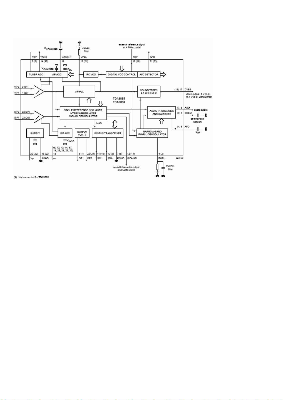
VIF amplifier, Tuner and VIF-AGC, VIF-AGC detector, Frequency Phase-Locked Loop (FPLL) detector, VCO and
divider, Digital acquisition help and AFC, Video demodulator and amplifier, Sound carrier trap, SIF amplifier, SIF-AGC
detector, Single reference QSS mixer, AM demodulator, FM demodulator and acquisition help, Audio amplifier and
mute time constant,I²C-bus transceivers and MAD (module address), Internal voltage stabilizer.
7. MULTI STANDARD SOUND PROCESSOR
The MSP34x0G family of single-chip Multistandard Sound Processors covers the sound processing of all analogue TVStandards worldwide, as well as the NICAM digital sound standards. The full TV sound processing, starting with analogue
sound IF signal-in, down to processed analogue AF-out, is performed on a single chip.
These TV sound processing ICs include versions for processing the multichannel television sound (MTS) signal
conforming to the standard recommended by the Broadcast Television Systems Committee (BTSC). The DBX
noise reduction, or alternatively, Micronas Noise Reduction (MNR) is performed alignment free. Other processed
standards are the Japanese FM-FM multiplex standard (EIA-J) and the FM Stereo Radio standard.
Current ICs have to perform adjustment procedures in order to achieve good stereo separation for BTSC and EIA-J. The
MSP 34x1G has optimum stereo performance without any adjustments.
8. VIDEO SWITCH TEA6415
In case of three or more external sources are used, the video switch IC TEA6415 is used. The main function of this device is
to switch 8 video-input sources on the 6 outputs.
Each output can be switched on only one of each input. On each input an alignment of the lowest level of the
signal is made (bottom of sync. top for CVBS or black level for RGB signals).
Each nominal gain between any input and output is 6.5dB.For D2MAC or Chroma signal the alignment is switched off by
forcing, with an external resistor bridge, 5VDC on the input. Each input can be used as a normal input or as a MAC or
Chroma input (with external Resistor Bridge). All the switching possibilities are changed through the BUS. Driving 75ohm
load needs an external resistor. It is possible to have the same input connected to several outputs.
9. AUDIO AMPLIFIER STAGE WITH TPA3004D2
The TPA3004D2 is a 12-W (per channel) efficient, Class-D audio amplifier for driving bridged-tied stereo speakers. The
TPA3004D2 can drive stereo speakers as low as 4 Ω. The high efficiency of the TPA3004D2 eliminates the need for
external heatsinks when playing music.
Stereo speaker volume is controlled with a dc voltage applied to the volume control terminal offering a range of gain from –
40 dB to 36 dB. Line outputs, for driving external headphone amplifier inputs, are also dc voltage controlled with a range
of gain from –56 dB to 20 dB.
An integrated 5-V regulated supply is provided for powering an external headphone amplifier.
8

10. POWER SUPPLY (SMPS)
The DC voltages required at various parts of the chassis are provided by an SMPS transformer controlled by the IC
MC44608, which is designed for driving, controlling and protecting switching transistor of SMPS. The transformer
generates 145V for FBT input, +/-14V for audio amplifier, 5V and 3.3V stand by voltage and 8V, 12V and 5V supplies for
other different parts of the chassis.
An optocoupler is used to control theregulation of line voltage and stand-by power consumption. There is a regulation
circuit in secondary side. This circuit produces a control voltage according to the changes in 145V DC voltage, via an
optocoupler (TCET1102G) to pin3 of the IC.
During the switch on period of the transistor, energy is stored in the transformer. During the switch off period
energy is fed to the load via secondary winding. By varying switch-on time of the power transistor, it controls
each portion of energy transferred to the second side such that the output voltage remains nearly independent
of load variations.
11. MICROCONTROLLER
The Micronas SDA 55xx TV microcontroller is dedicated to 8 bit applications for TV control and provides dedicated
graphic features designed for modern low class to mid range TV sets. The SDA 55xx provides also an integrated
general purposefully 8051-compatible microcontroller with specific hardware features especially suitable in TV sets.
The microcontroller core has been enhanced to provide powerful features such as memory banking, data pointers and
additional interrupts, etc. The internal XRAM consists of up to 16 kBytes. The microcontroller provides an internal
ROM of up to 128 kBytes. ROMless versions can access up to 1 MByte of external RAM and ROM. The 8-bit
microcontroller runs at 33.33 MHz internal clock. SDA 55xx is realized in 0.25 micron technology with 2.5 V supply
voltage for the core and 3.3 V for the I/O port pins to make them TTL compatible. Based on the SDA 55xx
microcontroller the MINTS software package was developed and provides dedicated device drivers for many Micronas
video & audio products and includes a full blown TV control SW for the PEPER application chassis. The SDA 55xx is
also supported with powerful design tools like emulators from Hitex, Kleinhenz, iSystems, the Keil C51 Compiler and
TEDIpro OSD development SW by Tara Systems.
12. SERIAL ACCESS CMOS 4Kx8(32KBit)EEPROM 24C32A
The Microchip Technology Inc. 24AA32A/24LC32A(24XX32A*) is a 32 Kbit Electrically Erasable PROM. The device is
organized as four blocks of 8K x 8-bitmemory with a 2-wire serial interface. Low-voltage design permits operation
down to 1.8V, with standby and active currents of only 1µA and 1mA, respectively. It has been developed for
advanced, low-power applications such as personal communications or data acquisition. The 24XX32A also has a
page write capability for up to 32 bytes of data. Functional address lines allow up to eight devices on the same bus, for
up to 256Kbits address space.
13. CLASS AB STEREO HEADPHONE DRIVER TDA1308
The TDA1308 is an integrated class AB stereo headphone driver contained in a DIP8 plastic package. The
device is fabricated in a 1 mm CMOS process and has been primarily developed for portable digital audio
applications.
14. SAW FILTERS
K9656M:
Standard:
• B/G
• D/K
• I
• L/L’
Features
• TV IF audio filter with two channels
• Channel 1 (L’) with one pass band for sound carriers at 40.40 MHz (L’) and 39.75 MHz (L’- NICAM)
• Channel 2 (B/G, D/K, L, I) with one pass band for sound carriers between 32.35 MHz and 33.40 MHz
Terminals
• Tinned CuFe alloy
Pin configuration
1 Input
2 Switching input
3 Chip carrier- ground
4 Output
5 Output
9

K3958M:
Standard:
• B/G
• D/K
• I
• L/L’
Features
• TV IF video filter with Nyquist slopes at 33.90 MHz and 38.90 MHz
• Constant group delay
Terminals
Tinned CuFe alloy
Pin configuration
1 Input
2 Input- ground
3 Chip carrier- ground
4 Output
5 Output
15. IC DESCRIPTIONS
TEA6415C
24LC02
24C32
74LVC14A
TEA6420D
CS4334
GAL16LV8
K6R4008V1
KA278R33
LM1117
LM317T
LM809
MSP3411G
M29W040B
MC33202
PCF8574
TSOP1836
PI5V330
SDA5550
SII9993
SN74CB3Q3305
ST24LC21
LM2576
MC34063
TDA1308
TDA9886T
TPA3004D2
µPA672T
VPC3230D
TEA6415C
General Description
The main function of the IC is to switch 8 video input sources on 6 outputs. Each output can be switched on only
one of each input. On each input an alignment of the lowest level of the signal is made (bottom of synch. top for
CVBS or black level for RGB signals). Each nominal gain between any input and output is 6.5dB. For D2MAC or
Chroma signal the alignment is switched off by forcing, with an external resistor bridge, 5 VDC on the input. Each
input can be used as a normal input or as a MAC or Chroma input (with external resistor bridge). All the
switching possibilities are changed through the BUS. Driving 75Ω load needs an external transistor. It is possible
to have the same input connected to several outputs. The starting configuration upon power on (power supply: 0
10

to 10V) is undetermined. In this case, 6 words of 16 bits are necessary to determine one configuration. In other
case, 1 word of 16 bits is necessary to determine one configuration.
Features
• 20MHz Bandwidth
• Cascadable with another TEA6415C (Internal address can be changed by pin 7 voltage)
• 8 Inputs (CVBS, RGB, MAC, CHROMA,...)
• 6 Outputs
• Possibility of MAC or chroma signal for each input by switching-off the clamp with an external resistor bridge
• Bus controlled
• 6.5dB gain between any input and output
• 55dB crosstalk at 5mHz
• Fully ESD protected
Pinning
1. Input : Max : 2Vpp, Input Current: 1mA, Max : 3mA
2. Data : Low level : -0.3V Max: 1.5V,
High level : 3.0V Max : Vcc+0.5V
3. Input : Max : 2Vpp, Input Current: 1mA, Max : 3mA
4. Clock : Low level : -0.3V Max: 1.5V,
High level : 3.0V Max : Vcc+0.5V
5. Input : Max : 2Vpp, Input Current: 1mA, Max : 3mA
6. Input : Max : 2Vpp, Input Current: 1mA, Max : 3mA
7. Prog
8. Input : Max : 2Vpp, Input Current: 1mA, Max: 3mA
9. Vcc : 12V
10. Input : Max : 2Vpp, Input Current: 1mA, Max : 3mA
11. Input : Max : 2Vpp, Input Current: 1mA, Max : 3mA
12. Ground
13. Output : 5.5Vpp, Min : 4.5Vpp
14. Output : 5.5Vpp, Min : 4.5Vpp
15. Output : 5.5Vpp, Min : 4.5Vpp
16. Output : 5.5Vpp, Min : 4.5Vpp
17. Output : 5.5Vpp, Min : 4.5Vpp
18. Output : 5.5Vpp, Min : 4.5Vpp
19. Ground
20. Input : Max : 2Vpp, Input Current : 1mA, Max : 3mA
11
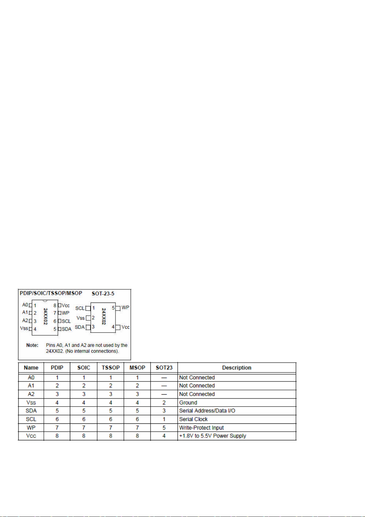
15.1. 24LC02
15.1.1. Description
The Microchip Technology Inc. 24AA02/24LC02B (24XX02*) is a 2 Kbit Electrically Erasable PROM. The device
is organized as one block of 256 x 8-bit memory with a 2-wire serial interface. Low-voltage design permits
operation down to 1.8V, with standby and active currents of only 1µA and 1mA, respectively. The 24XX02 also
has a page write capability for up to 8 bytes of data.
15.1.2. Features
• Single supply with operation down to 1.8V
• Low-power CMOS technology
-1mA active current typical
-1µA standby current typical (I-temp)
• Organized as 1 block of 256 bytes (1 x 256 x 8)
• 2-wire serial interface bus, I2C™ compatible
• Schmitt Trigger inputs for noise suppression
• Output slope control to eliminate ground bounce
• 100 kHz (24AA02) and 400 kHz (24LC02B) compatibility
• Self-timed write cycle (including auto-erase)
• Page write buffer for up to 8 bytes
• 2ms typical write cycle time for page write
• Hardware write-protect for entire memory
• Can be operated as a serial ROM
• Factory programming (QTP) available
• ESD protection > 4,000V
• 1,000,000 erase/write cycles
• Data retention > 200 years
• 8-lead PDIP, SOIC, TSSOP and MSOP packages
• 5-lead SOT-23 package
• Pb-free finish available
• Available for extended temperature ranges:
-Industrial (I): -40°C to +85°C
-Automotive (E):-40°C to +125°C
15.1.3. Pinning
12
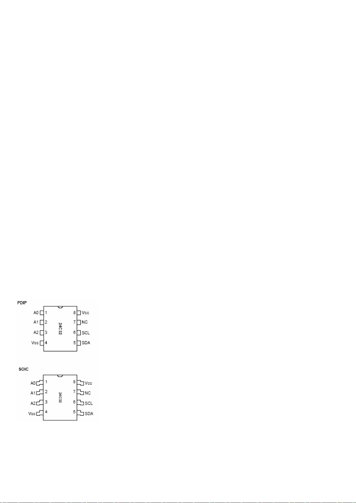
15.2. 24C32
15.2.1. General Description
The Microchip Technology Inc. 24C32 is a 4K x 8 (32K bit) Serial Electrically Erasable PROM. This device has
been developed for advanced, low power applications such as personal communications or data acquisition.
The 24C32 features an input cache for fast write loads with a capacity of eight 8-byte pages, or 64 bytes. It also
features a fixed 4K-bit block of ultra-high endurance memory for data that changes frequently. The 24C32 is
capable of both random and sequential reads up to the 32K boundary. Functional address lines allow up to 8 24C32 devices on the same bus, for up to 256K bits address space. Advanced CMOS technology makes this
device ideal for low-power non-volatile code and data applications.
15.2.2. Features
• Voltage operating range: 4.5V to 5.5V
- Peak write current 3 mA at 5.5V
- Maximum read current 150µA at 5.5V
- Standby current 1µA typical
• Industry standard two-wire bus protocol, I2C™ compatible
-Including 100 kHz and 400 kHz modes
• Self-timed write cycle (including auto-erase)
• Power on/off data protection circuitry
• Endurance:
- 10,000,000 Erase/Write cycles guaranteed for High Endurance Block
- 10,000,000 E/W cycles guaranteed for Standard Endurance Block
• 8 byte page, or byte modes available
• 1page x 8 lineinput cache (64bytes) for fast write
loads
• Schmitt trigger, filtered inputs for noise suppression
• Output slope control to eliminate ground bounce
• 2 ms typical write cycle time, byte or page
• Up to 8 chips may be connected to the same bus for up to 256K bits total memory
• Electrostatic discharge protection > 4000V
• Data retention > 200 years
• Temperature ranges:
-Commercial (C): 0°C to +70°C
-Industrial (I): -40°C to +85°C
15.2.3. Pinning
13
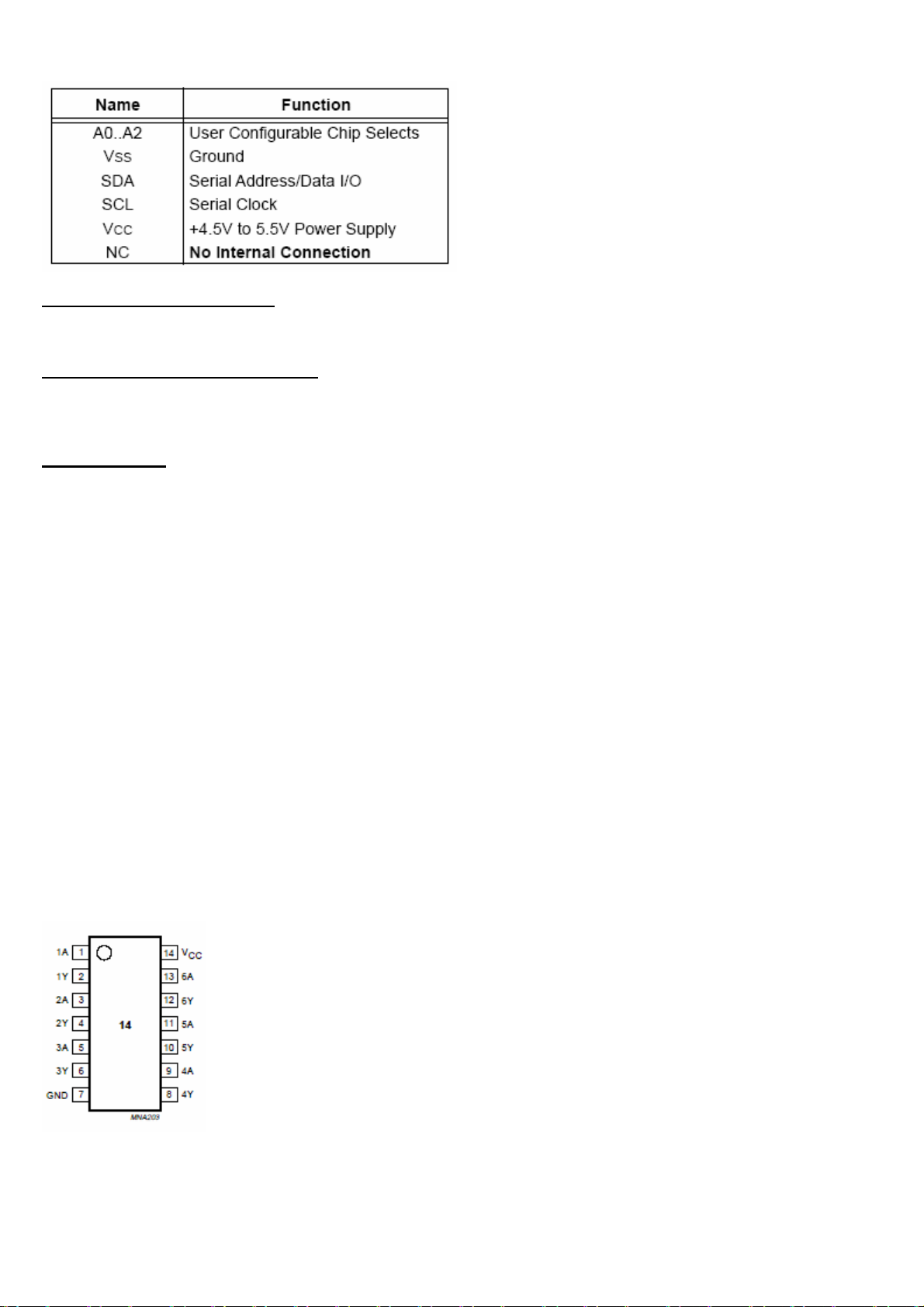
15.2.4. PIN Function Table
PIN DESCRIPTIONS
A0, A1, A2 Chip Address Inputs
The A0...A2 inputs are used by the 24C32 for multiple device operation and conform to the two-wire bus standard. The levels applied to these pins define the address block occupied by the device in the address map. A
particular device is selected by transmitting the corresponding bits (A2, A1, and A0) in the control byte.
SDA Serial Address/Data Input/Output
This is a bidirectional pin used to transfer addresses and data into and data out of the device. It is an open drain
terminal; therefore the SDA bus requires a pull-up resistor to VCC (typical 10KQ for 100 kHz, 1KQ for 400 kHz).
For normal data transfer SDA is allowed to change only during SCL low. Changes during SCL high are reserved
for indicating the START and STOP conditions.
SCL Serial Clock
This input is used to synchronize the data transfer from and to the device.
15.3. 74LVC14A
15.3.1. Description
The 74LVC14A is a high-performance, low-power, low-voltage, Si-gate CMOS device, superior to most advanced
CMOS compatible TTL families. Inputs can be driven from either 3.3 or 5V devices. This feature allows the use of
these devices as translators in a mixed 3.3 and 5V environment. The 74LVC14A provides six inverting buffers with
Schmitt-trigger action. It is capable of transforming slowly changing input signals into sharply defined, jitter-free output
signals.
15.3.2. Features
• Wide supply voltage range from 1.2 to 3.6 V
• CMOS low power consumption
• Direct interface with TTL levels
• Inputs accept voltages up to 5.5 V
• Complies with JEDEC standard no.8-1A
• ESD protection:
HBM EIA/JESD22-A114-A exceeds 2000V
MM EIA/JESD22-A115-A exceeds 200V.
• Specified from-40 to +85C and -40 to +125C.
15.3.3. Pinning
14
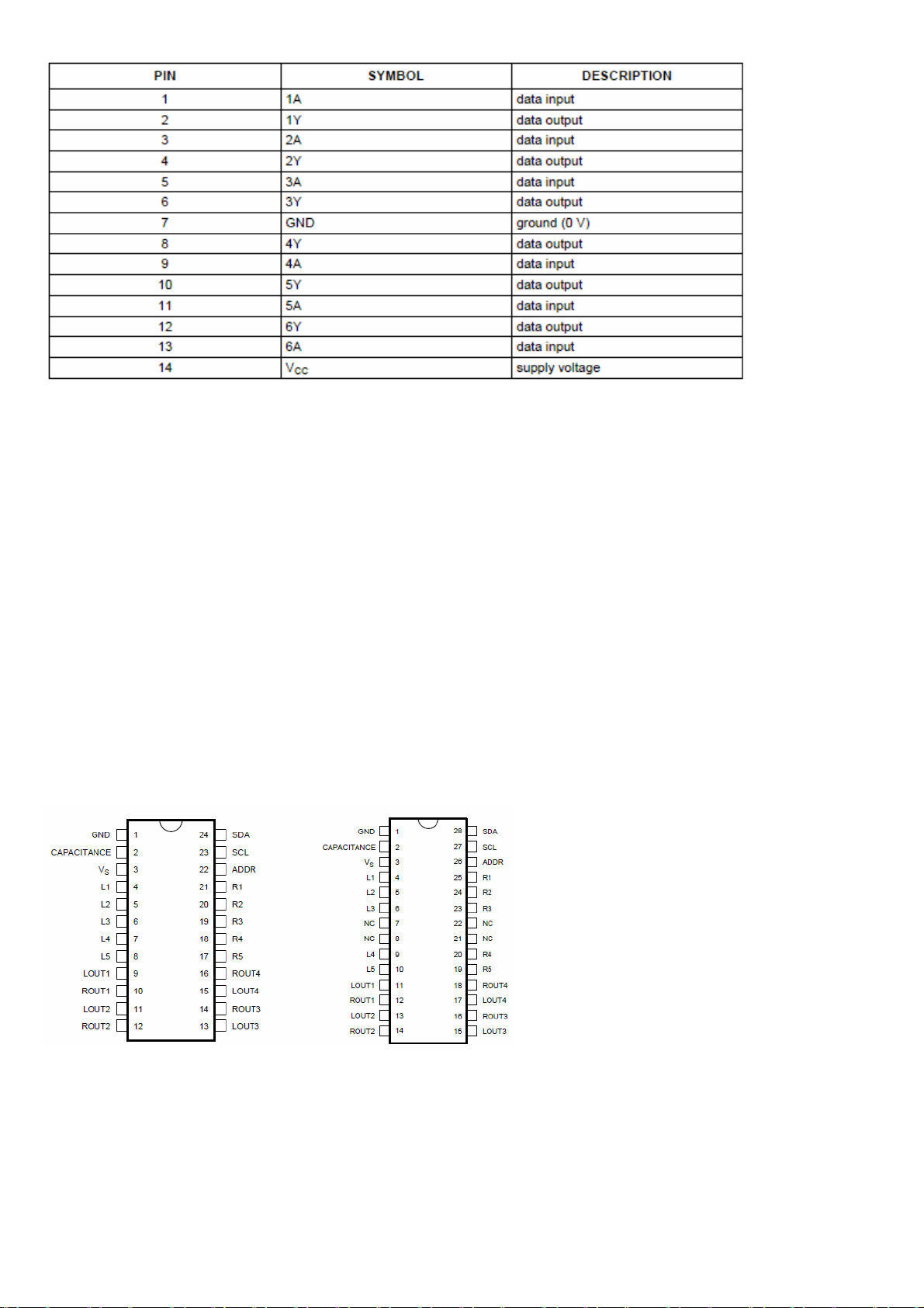
15.4. TEA6420
15.4.1. Features
• 5 Stereo Inputs
• 4 Stereo Outputs
• Gain Control 0/2/4/6dB/Mute for each Output
• Cascadable (2 different addresses)
• Serial Bus Controlled
• Very low Noise
• Very low Distortion
15.4.2. Description
The TEA6420 switches 5 stereo audio inputs on4stereo outputs. All the switching possibilities are changed
through the I2C bus.
15.4.3. Pin Connections
15.5. CS4334
15.5.1. Features
• Complete Stereo DAC System: Interpolation, D/A, Output Analog Filtering
• 24-Bit Conversion
15
• 96 dB Dynamic Range
• -88 dB THD+N
• Low Clock Jitter Sensitivity
• Single +5V Power Supply
• Filtered Line Level Outputs
• On-Chip Digital De-emphasis
• Popgaurd® Technology
• Functionally Compatible with CS4330/31/33
15.5.2. General Description
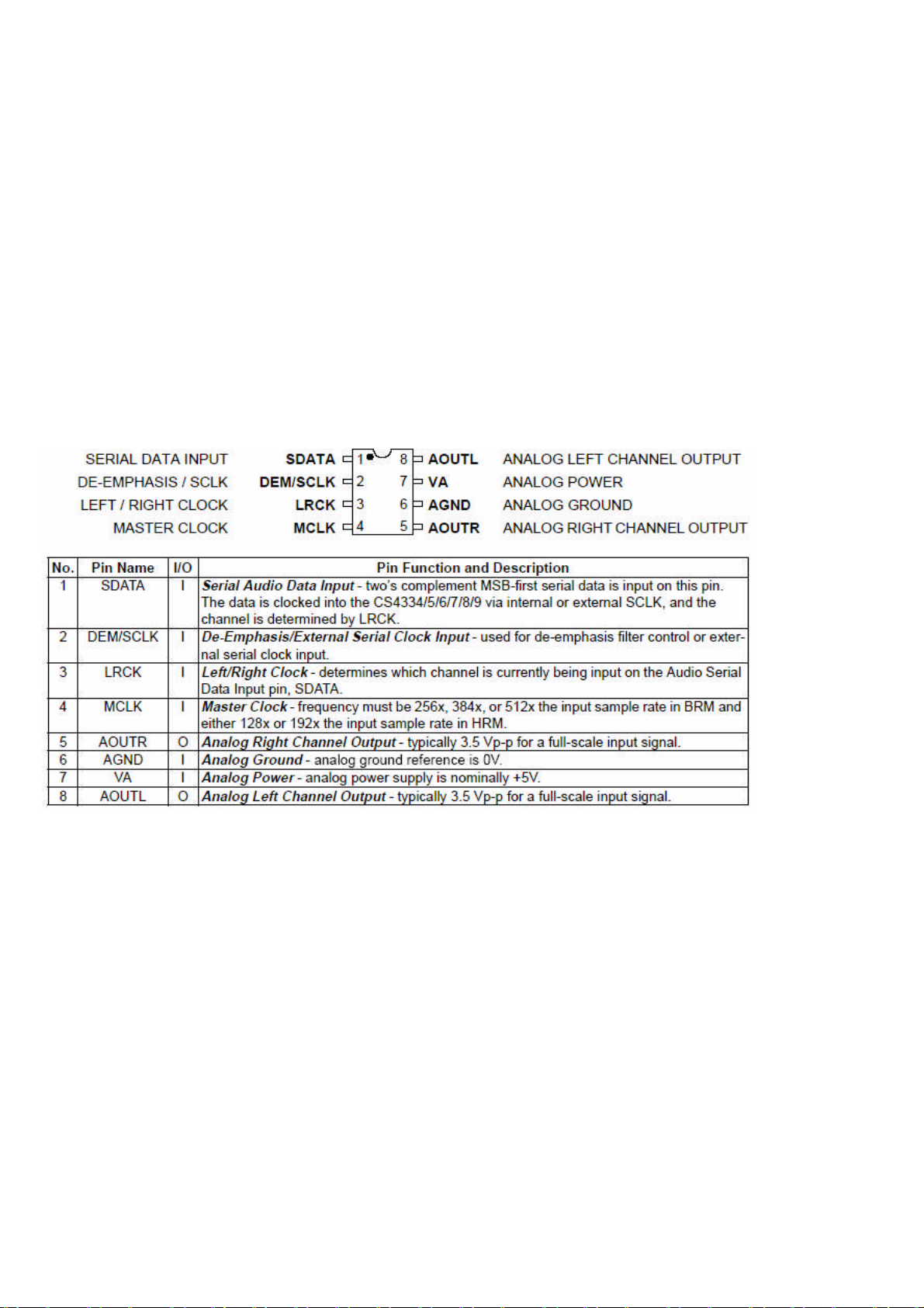
The CS4334 family members are complete, stereo digital-to-analog output systems including interpolation, 1bitD/A conversion and output analog filtering in an 8-pinpackage. The CS4334/5/6/7/8/9 support all major audio
data interface formats, and the individual devices differ only in the supported interface format. The CS4334
family is based on delta-sigma modulation, where the modulator output controls the reference voltage input to
an ultra-linear analog low-pass filter. This architecture allows for infinite adjustment of sample rate between 2
kHz and 100 kHz simply by changing the master clock frequency. The CS4334 family contains on-chip digital
de-emphasis, operates from a single +5V power supply, and requires minimal support circuitry. These features
are ideal for set-top boxes, DVD players, SVCD players, and A/V receivers.
15.5.3. Pin Descriptions
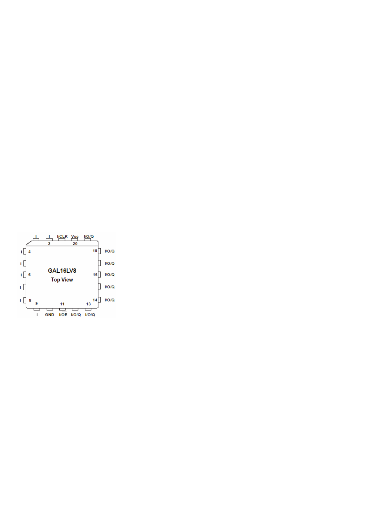
15.6. GAL16LV8
15.6.1. Description
The GAL16LV8D, at 3.5 ns maximum propagation delay time, provides the highest speed performance available
in the PLD market. The GAL16LV8C can interface with both 3.3V and 5Vsignal levels. The GAL16LV8 is
manufactured using Lattice Semiconductor's advanced 3.3V E2CMOS process, which combines CMOS with
Electrically Erasable (E2) floating gate technology. High speed erase times (<100ms) allow the devices to be
reprogrammed quickly and efficiently.
The 3.3V GAL16LV8 uses the same industry standard 16V8 architecture as its 5V counterpart and supports all
architectural features such as combinatorial or registered macrocell operations.
Unique test circuitry and reprogrammable cells allow complete AC, DC, and functional testing during
manufacture. As a result, Lattice Semiconductor delivers 100% field programmability and functionality of all
GAL products. In addition, 100 erase/write cycles and data retention in excess of 20 years are specified.
15.6.2. Features
• HIGH PERFORMANCE E2CMOS® TECHNOLOGY
- 3.5 ns Maximum Propagation Delay
- Fmax = 250 MHz
16
- 2.5 ns Maximum from Clock Input to Data Output
- UltraMOS® Advanced CMOS Technology
• 3.3V LOW VOLTAGE 16V8 ARCHITECTURE
- JEDEC-Compatible 3.3V Interface Standard
- 5V Compatible Inputs
- I/O Interfaces with Standard 5V TTL Devices (GAL16LV8C)
• ACTIVE PULL-UPS ON ALL PINS (GAL16LV8D Only)
• E2 CELL TECHNOLOGY
- Reconfigurable Logic
- Reprogrammable Cells
- 100% Tested/100% Yields
- High Speed Electrical Erasure (<100ms)
- 20 Year Data Retention
• EIGHT OUTPUT LOGIC MACROCELLS
- Maximum Flexibility for Complex Logic Designs
- Programmable Output Polarity
• PRELOAD AND POWER-ON RESET OF ALL REGISTERS
- 100% Functional Testability
• APPLICATIONS INCLUDE:
- Glue Logic for 3.3V Systems
- DMA Control
- State Machine Control
- High Speed Graphics Processing
- Standard Logic Speed Upgrade
• ELECTRONIC SIGNATURE FOR IDENTIFICATION
• LEAD-FREE PACKAGE OPTIONS
15.6.3. Pin connections
15.7.
15.8. K6R4008V1D
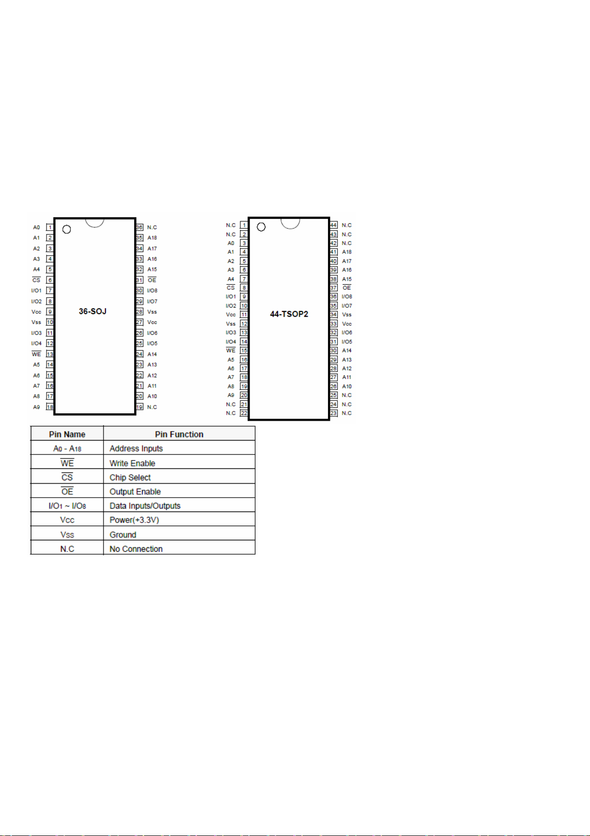
15.8.1. Description
The K6R4008V1D is a 4,194,304-bit high-speed Static Random Access Memory organized as 524,288 words by
8 bits. TheK6R4008V1D uses 8 common input and output lines and has an output enable pin which operates
faster than address access time at read cycle. The device is fabricated using SAMSUNG's advanced CMOS
process and designed for high-speed circuit technology. It is particularly well suited for use in high-density high-
speed system applications. The K6R4008V1D is packaged in a 400 mil 36-pin plastic SOJ and 44-pin plastic
TSOP type II.
15.8.2. Features
• Fast Access Time 8, 10ns(Max.)
• Low Power Dissipation
- Standby (TTL) : 20mA(Max.)
(CMOS) : 5mA(Max.)
- Operating K6R4008V1D-08 : 80mA(Max.)
17
K6R4008V1D-10 : 65mA(Max.)
• Single 3.3 ±0.3V Power Supply
• TTL Compatible Inputs and Outputs
• Fully Static Operation
- No Clock or Refresh required
• Three State Outputs
• Center Power/Ground Pin Configuration
• Standard Pin Configuration
K6R4008V1D-J : 36-SOJ-400
K6R4008V1D-K : 36-SOJ-400(Lead-Free)
K6R4008V1D-T : 44-TSOP2-400BF
K6R4008V1D-U : 44-TSOP2-400BF(Lead-Free)
• Operating in Commercial and Industrial Temperature range.
15.8.3. Pin Description
15.9. KA278R33
15.9.1. Features
• 2A / 3.3V Output low dropout voltage regulator
• TO220 Full-Mold package (4PIN)
• Overcurrent protection, Thermal shutdown
• Overvoltage protection, Short-Circuit protection
• With output disable function
15.9.2. Description
The KA278R33 is a low-dropout voltage regulator suitable for various electronic equipments. It provides
constant voltage power source with TO-220 4 lead full mold package. Dropout voltage of KA278R33 is below
18
0.5V in full rated current (2A). This regulator has various function such as peak current protection, thermal shut
down, overvoltage protection and output disable function.
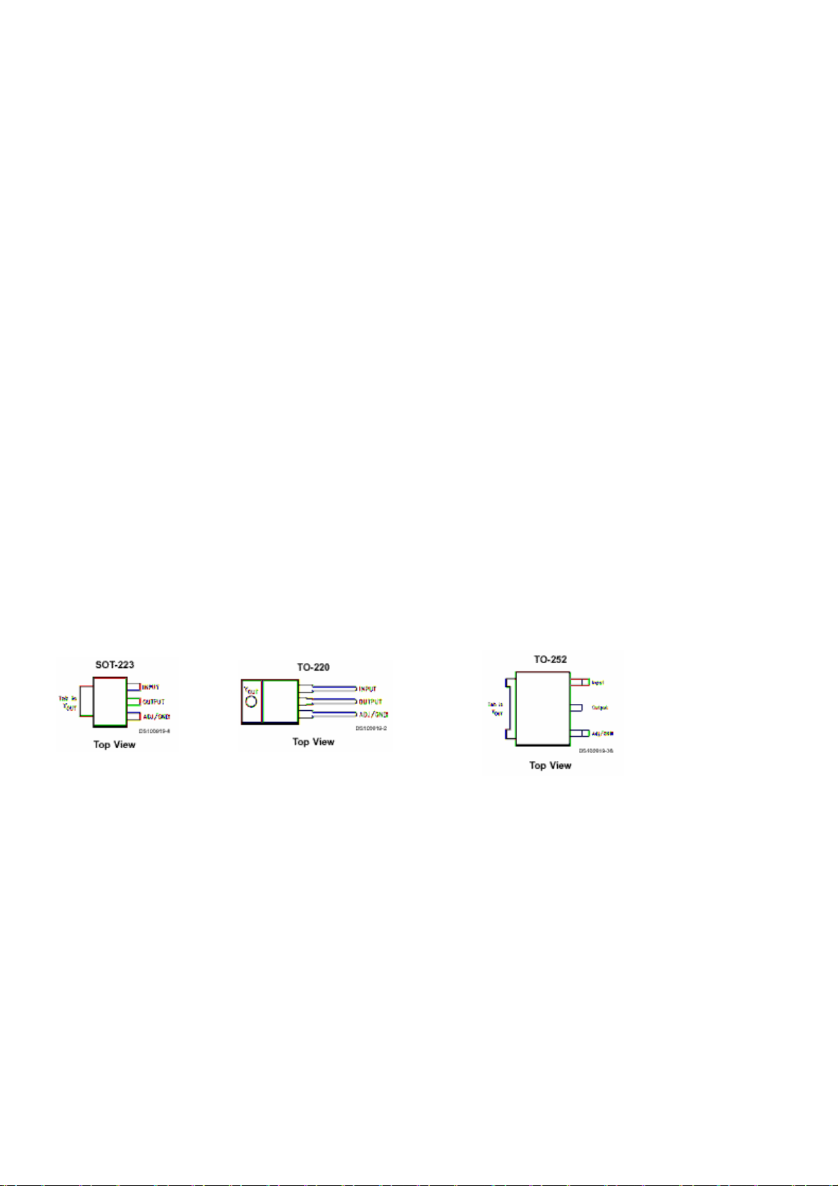
15.10. LM1117
15.10.1. General Description
The LM1117 is a series of low dropout voltage regulators with a dropout of 1.2V at 800mA of load current. It has the same
pin-out as National Semiconductor’s industry standard LM317. The LM1117 is available in an adjustable version, which
can set the output voltage from 1.25V to 13.8V with only two external resistors. In addition, it is also available in five fixed
voltages, 1.8V, 2.5V, 2.85V, 3.3V, and 5V.
The LM1117 offers current limiting and thermal shutdown. Its circuit includes a zener trimmed bandgap
reference to as-sure output voltage accuracy to within ±1%. The LM1117 series is available in SOT-223, TO-
220, and TO-252 D-PAK packages. A minimum of 10µF tantalum capacitor is required at the output to improve
the transient response and stability.
15.10.2. Features
• Available in 1.8V, 2.5V, 2.85V, 3.3V, 5V, and Adjustable Versions
• Space Saving SOT-223 Package
• Current Limiting and Thermal Protection
• Output Current 800mA
• Line Regulation 0.2% (Max)
• Load Regulation 0.4% (Max)
• Temperature Range
—LM1117 0°C to 125°C
—LM1117I -40°C to 125°C
15.10.3. Applications
• 2.85V Model for SCSI-2 Active Termination
• Post Regulator for Switching DC/DC Converter
• High Efficiency Linear Regulators
• Battery Charger
• Battery PoweredInstrumentation
Connection Diagrams
15.11. LM317
15.11.1. General Description
This monolithic integrated circuit is an adjustable 3-terminal positive voltage regulator designed to supply more
than 1.5A of load current with an output voltage adjustable over a 1.2 to 37V. It employs internal current limiting,
thermal shut-down and safe area compensation.
15.11.2. Features
• Output Current In Excess of 1.5A
• Output Adjustable Between 1.2V and 37V
• Internal Thermal Overload Protection
• Internal Short Circuit Current Limiting
• Output Transistor Safe Operating Area Compensation
• TO-220 Package
19
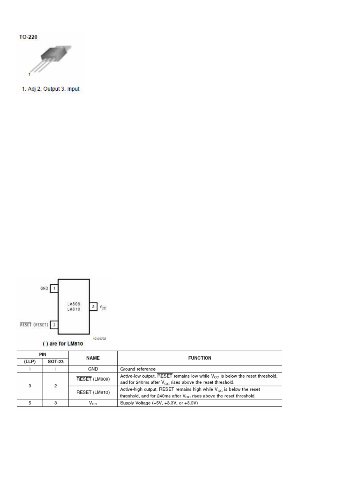
15.11.3. Pin Description
15.12. LM809
15.12.1. General Description
The LM809/810 microprocessor supervisory circuits can be used to monitor the power supplies in microprocessor and
digital systems. They provide a reset to the microprocessor during power-up, power-down and brown-out conditions.
The function of the LM809/810 is to monitor the VCC supply voltage, and assert a reset signal whenever this voltage
declines below the factory-programmed reset threshold. The reset signal remains asserted for 240 ms after VCC rises
above the threshold. The LM809 has an active-low RESET output, while the LM810 has an active-high RESET output.
Seven standard reset voltage options are available, suitable for monitoring 5V, 3.3V, and 3V supply voltages. With a
low supply current of only 15µA, the LM809/810 are ideal for use in portable equipment.
15.12.2. Features
• Precise monitoring of 3V, 3.3V, and 5V supply voltages
• Superior upgrade to MAX809/810
• Fully specified overtemperature
• 140 ms min. Power-On Reset pulse width, 240 ms typical
Active-low RESET Output(LM809)
Active-high RESET Output(LM810)
• Guaranteed RESET Output valid for VCC≥1V
• Low Supply Current, 15µAtyp
• Power supply transient immunity
15.12.3. Pinning
15.13. MSP34X1G (MSP3411G)
Multistandard Sound Processor Family
20
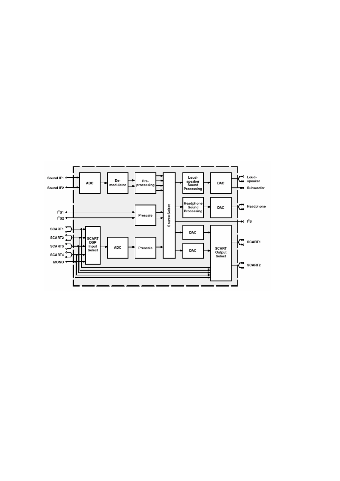
15.13.1. Introduction
The MSP 34x1G family of single-chip Multistandard Sound Processors covers the sound processing of all
analog TV-Standards worldwide, as well as the NICAM digital sound standards. The full TV sound processing,
starting with analog sound IF signal-in, down to processed analog AF-out, is performed on a single chip. Figure
shows a simplified functional block diagram of the MSP 34x1G.
The MSP 34x1G has all functions of the MSP 34x0G with the addition of a virtual surround sound feature.
Surround sound can be reproduced to a certain extent with two loudspeakers. The MSP 34x1G includes the
Micronas virtualizer algorithm “3D-PANORAMA” which has been approved by the Dolby 1) Laboratories for with
the "Virtual Dolby Surround" technology. In addition, the MSP 34x1G includes the “PAN-ORAMA” algorithm.
These TV sound processing ICs include versions for processing the multichannel television sound (MTS) signal conforming
to the standard recommended by the Broadcast Television Systems Committee (BTSC). The DBX noise reduction, or
alternatively, Micronas Noise Reduction (MNR) is performed alignment free.
Other processed standards are the Japanese FM-FM multiplex standard (EIA-J) and the FM Stereo Radio
standard.
Current ICs have to perform adjustment procedures in order to achieve good stereo separation for BTSC and
EIA-J. The MSP 34x1G has optimum stereo performance without any adjustments.
The MSP 34x1G has built-in automatic functions: The IC is able to detect the actual sound standard automatically (Automatic Standard Detection). Furthermore, pilot levels and identification signals can be evaluated
internally with subsequent switching between mono/stereo/bilingual; no I 2 C interaction is necessary (Automatic
Sound Selection).
Source Select
I2S bus interface consists of five pins:
1. I2S_DA_IN1, I2S_DA_IN2: For input, four channels (two channels per line, 2*16 bits) per sampling cycle (32
kHz) are transmitted.
2. I2S_DA_OUT: For output, two channels (2*16 bits) per sampling cycle (32 kHz) are transmitted.
3. I2S_CL: Gives the timing for the transmission of I2S serial data (1.024 MHz).
4. I2S_WS: The I2S_WS word strobe line defines the left and right sample.
15.13.2. Features
• Standard Selection with single I2C transmission
• Automatic Standard Detection of terrestrial TV standards
• Automatic Sound Selection (mono/stereo/bilingual), new registers MODUS, STATUS
• Two selectable sound IF (SIF) inputs
• Automatic Carrier Mute function
• Interrupt output programmable (indicating status change)
• Loudspeaker / Headphone channel with volume, balance, bass, treble, loudness
• AVC: Automatic Volume Correction
• Subwoofer output with programmable low-pass and complementary high-pass filter
• 5-band graphic equalizer for loudspeaker channel
• Spatial effect for loudspeaker channel
• Four Stereo SCART (line) inputs, one Mono input; two Stereo SCART outputs
21

• Complete SCART in/out switching matrix
• Two I2S inputs; one I2S output
• Dolby Pro Logic with DPL 351xA coprocessor
• All analog FM-Stereo A2 and satellite standards; AM-SECAM L standard
• Simultaneous demodulation of (very) high-deviation FM-Mono and NICAM
• Adaptive deemphasis for satellite (Wegener-Panda, acc. to ASTRA specification)
• ASTRA Digital Radio (ADR) together with DRP 3510A
• All NICAM standards
• Korean FM-Stereo A2 standard
Pin connections
NC = not connected; leave vacant
LV = if not used, leave vacant
OBL = obligatory; connect as described in circuit diagram
DVSS: if not used, connect to DVSS
AHVSS: connect to AHVSS
Pin No. Pin Name Type
PLCC
68-pin
1 16 14 9 8 ADR_WS OUT LV ADR word strobe
2 - - - - NC LV Not connected
3 15 13 8 7 ADR_DA OUT LV ADR Data Output
4 14 12 7 6 I2S_DA_IN1 IN LV I2S1 data input
5 13 11 6 5 I2S_DA_OUT OUT LV I2S data output
6 12 10 5 4 I2S_WS IN/OUT LV I2S word strobe
7 11 9 4 3 I2S_CL IN/OUT LV I2S clock
8 10 8 3 2 I2C_DA IN/OUT OBL I2C data
9 9 7 2 1 I2C_CL IN/OUT OBL I2C clock
10 8 - 1 64 NC LV Not connected
11 7 6 80 63 STANDBYQ IN OBL Stand-by (low-active)
12 6 5 79 62 ADR_SEL IN OBL I2C bus address select
13 5 4 78 61 D_CTR_I/O_0 IN/OUT LV D_CTR_I/O_0
14 4 3 77 60 D_CTR_I/O_1 IN/OUT LV D_CTR_I/O_1
15 3 - 76 59 NC LV Not connected
16 2 - 75 58 NC LV Not connected
17 - - - - NC LV Not connected
18 1 2 74 57 AUD_CL_OUT OUT LV
19 64 1 73 56 TP LV Test pin
20 63 52 72 55 XTAL_OUT OUT OBL Crystal oscillator
21 62 51 71 54 XTAL_IN IN OBL Crystal oscillator
22 61 50 70 53 TESTEN IN OBL Test pin
23 60 49 69 52 ANA_IN2+ IN
24 59 48 68 51 ANA_IN- IN
25 58 47 67 50 ANA_IN1+ IN LV IF input1
26 57 46 66 49 AVSUP OBL Analog powersupply 5V
- - - 65 - AVSUP OBL Analog powersupply 5V
- - - 64 - NC LV Not connected
- - - 63 - NC LV Not connected
27 56 45 62 48 AVSS OBL Analog ground
- - - 61 - AVSS OBL Analog ground
28 55 44 60 47 MONO_IN IN LV Mono input
- - - 59 - NC LV Not connected
29 54 43 58 46 VREFTOP OBL
30 53 42 57 45 SC1_IN_R IN LV SCART 1 input, right
31 52 41 56 44 SC1_IN_L IN LV SCART 1 input, left
32 51 - 55 43 ASG1 AHVSS Analog Shield Ground 1
33 50 40 54 42 SC2_IN_R IN LV SCART 2 input, right
34 49 39 53 41 SC2_IN_L IN LV SCART 2 input, left
35 48 - 52 40 ASG2 AHVSS Analog Shield Ground 2
36 47 38 51 39 SC3_IN_R IN LV SCART 3 input, right
PSDIP
64-pin
PSDIP
52-pin
PQFP
80-pin
PLQFP
64-pin
Connection
(if not used)
AVSS via
56 pF/LV
AVSS via
56 pF/LV
Short Description
Audio clock output
(18.432 MHz)
IF Input 2 (can be left
vacant, onlyif IF input 1 is
also notin use)
IF common (can be left
vacant, onlyif IF input 1 is
also notin use)
Reference voltage IF A/D
converter
22

37 46 37 50 38 SC3_IN_L IN LV SCART 3 input, left
38 45 - 49 37 ASG4 AHVSS Analog Shield Ground 4
39 44 - 48 36 SC4_IN_R IN LV SCART 4 input, right
40 43 - 47 35 SC4_IN_L IN LV SCART 4 input, left
41 - - 46 - NC LV or AHVSS Not connected
42 42 36 45 34 AGNDC OBL Analog reference voltage
43 41 35 44 33 AHVSS OBL Analog ground
- - - 43 - AHVSS OBL Analog ground
- - - 42 - NC LV Not connected
- - - 41 - NC LV Not connected
44 40 34 40 32 CAPL_M OBL Volume capacitor MAIN
45 39 33 39 31 AHVSUP OBL Analog powersupply 8V
46 38 32 38 30 CAPL_A OBL Volume capacitorAUX
47 37 31 37 29 SC1_OUT_L OUT LV SCART output 1,left
48 36 30 36 28 SC1_OUT_R OUT LV SCART output 1, right
49 35 29 35 27 VREF1 OBL Reference ground1
50 34 28 34 26 SC2_OUT_L OUT LV SCART output 2,left
51 33 27 33 25 SC2_OUT_R OUT LV SCART output 2, right
52 - - 32 - NC LV Not connected
53 32 - 31 24 NC LV Not connected
54 31 26 30 23 DACM_SUB OUT LV Subwoofer output
55 30 - 29 22 NC LV Not connected
56 29 25 28 21 DACM_L OUT LV Loudspeaker out, left
57 28 24 27 20 DACM_R OUT LV Loudspeaker out, right
58 27 23 26 19 VREF2 OBL Reference ground2
59 26 22 25 18 DACA_L OUT LV Headphone out, left
60 25 21 24 17 DACA_R OUT LV Headphone out, right
- - - 23 - NC LV Not connected
- - - 22 - NC LV Not connected
61 24 20 21 16 RESETQ IN OBL Power-on-reset
62 23 - 20 15 NC LV Not connected
63 22 - 19 14 NC LV Not connected
64 21 19 18 13 NC LV Not connected
65 20 18 17 12 I2S_DA_IN2 IN LV I2S2-data input
66 19 17 16 11 DVSS OBL Digital ground
- - - 15 - DVSS OBL Digital ground
- - - 14 - DVSS OBL Digital ground
67 18 16 13 10 DVSUP OBL Digital power supply 5V
- - - 12 - DVSUP OBL Digital power supply 5V
- - - 11 - DVSUP OBL Digital power supply 5V
68 17 15 10 9 ADR_CL OUT LV ADR clock
15.14. M29W040B
15.14.1. Description
The M29W040B is a 4 Mbit (512Kb x8) non-volatile memory that can be read, erased and reprogrammed. These operations
can be performed using a single low voltage (2.7 to 3.6V) supply. On power-up the memory defaults to its Read mode
where it can be read in the same way as a ROM or EPROM. The M29W040B is fully backward compatible with the
M29W040.The memory is divided into blocks that can be erased independently so it is possible to preserve valid data while
old data is erased. Each block can be protected independently to prevent accidental Program or Erase commands from
modifying the memory. Program and Erase commands are writ-ten to the Command Interface of the memory. An on-chip
Program/Erase Controller simplifies the process of programming or erasing the memory by taking care of all of the special
operations that are required to update the memory contents. The end of a program or erase operation can be detected and
any error conditions identified. The command set required to control the memory is consistent with JEDEC standards. Chip
Enable, Output Enable and Write Enable signals control the bus operation of the memory. They allow simple connection to
most microprocessors, often without additional logic.
15.14.2. Features
• SINGLE 2.7 to 3.6V SUPPLY VOLTAGE for PROGRAM, ERASE and READ OPERATIONS
• ACCESS TIME: 55ns
• PROGRAMMING TIME
- 10µs per Byte typical8
•UNIFORM 64 Kbytes MEMORY BLOCKS
• PROGRAM/ERASE CONTROLLER
- Embedded Byte Program algorithm
- Embedded Multi-Block/Chip Erase algorithm
- Status Register Polling and Toggle Bits
23
• ERASE SUSPEND and RESUME MODES
- Read and Program another Block during Erase Suspend
•UNLOCK BYPASS PROGRAM COMMAND
- Faster Production/Batch Programming
•LOW POWER CONSUMPTION
- Standby and Automatic Standby
•100,000 PROGRAM/ERASE CYCLES per BLOCK
•20 YEARS DATA RETENTION
- Defectivity below 1 ppm/year
• ELECTRONIC SIGNATURE
- Manufacturer Code: 20h
- Device Code: E3h
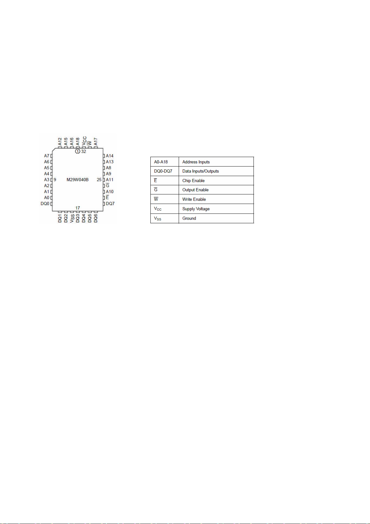
15.14.3. Pin Descriptions
15.15. MC33202
15.15.1. General Description
The MC33201/2/4 family of operational amplifiers provide rail−to−rail operation on both the input and output.
The inputs can be driven as high as 200mV beyond the supply rails without phase reversal on the outputs, and
the output can swing within 50 mV of each rail. This rail−to−rail operation enables the user to make full use of
the supply voltage range available. It is designed to work at very low supply voltages (±0.9 V) yet can operate
with a supply of up to +12V and ground. Output current boosting techniques provide a high output current
capability while keeping the drain current of the amplifier to a minimum. Also, the combination of low noise and
distortion with a high slew rate and drive capability make this an ideal amplifier for audio applications.
15.15.2. Features
• Low Voltage, Single Supply Operation (+1.8 V and Ground to +12 V and Ground)
• Input Voltage Range Includes both Supply Rails
• Output Voltage Swings within 50 mV of both Rails
• No Phase Reversal on the Output for Over−driven Input Signals
• High Output Current (ISC = 80 mA, Typ)
• Low Supply Current (ID = 0.9 mA, Typ)
• 600Ω Output Drive Capability
• Extended Operating Temperature Ranges (−40° to +105°C and −55° to +125°C)
• Typical Gain Bandwidth Product = 2.2 MHz
• Pb−Free Packages are Available
24
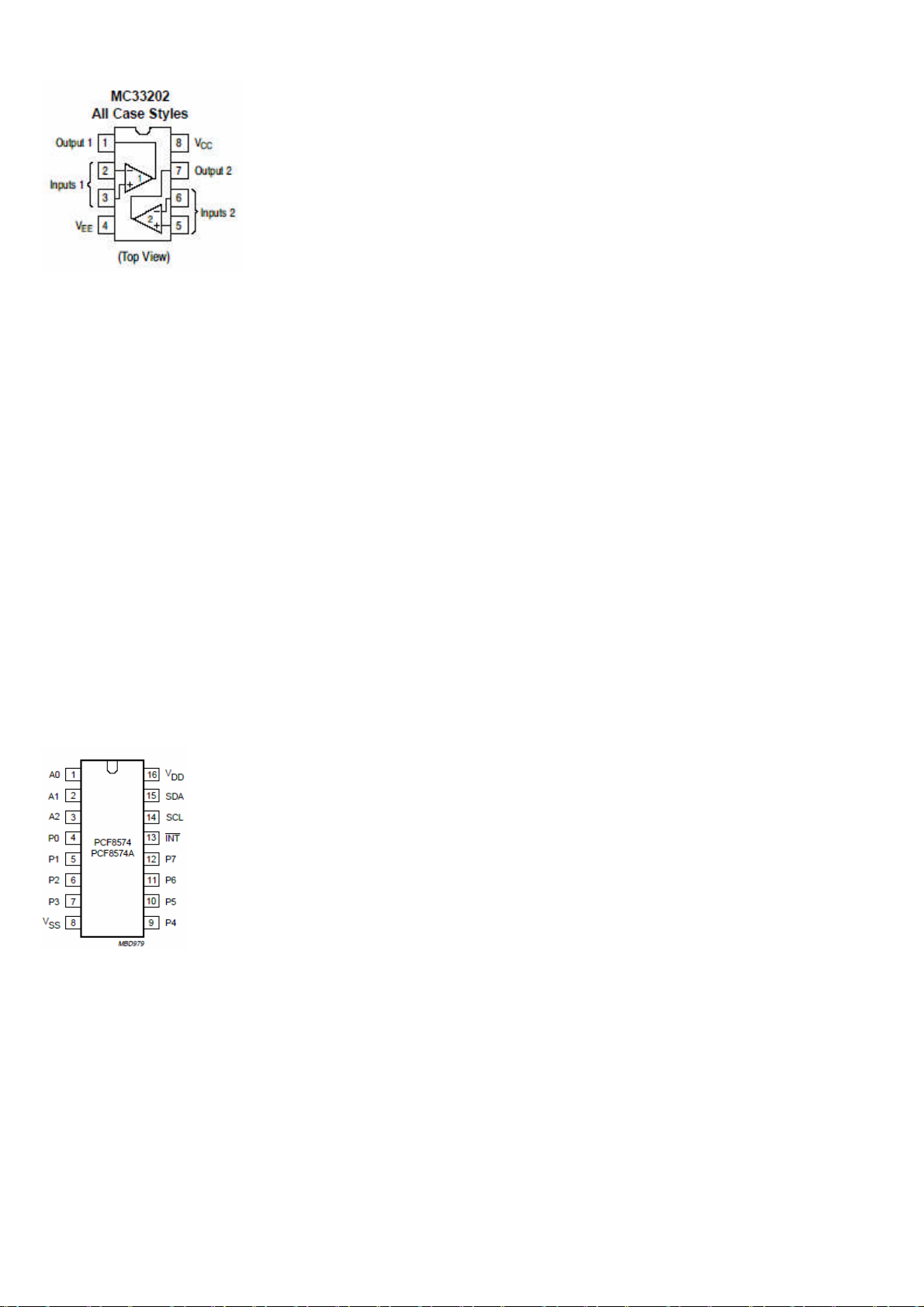
15.15.3. Pin Connections
15.16. PCF8574
15.16.1. General Description
The PCF8574 is a silicon CMOS circuit. It provides general purpose remote I/O expansion for most microcontroller
families via the two-line bidirectional bus (I2C).The device consists of an 8-bit quasi-bidirectional port and an I2C-bus
interface. The PCF8574 has a low current consumption and includes latched outputs with high current drive capability for
directly driving LEDs. It also possesses an interrupt line (INT) which can be connected to the interrupt logic of the
microcontroller. By sending an interrupt signal on this line, the remote I/O can inform the microcontroller if there is
incoming data on its ports without having to communicate via the I2C-bus. This means that the PCF8574 can remain a
simple slave device.
15.16.2. Features
• Operating supply voltage 2.5 to 6V
• Low standby current consumption of 10 µA maximum
• I2C to parallel port expander
• Open-drain interrupt output
• 8-bit remote I/O port for the I2C-bus
• Compatible with most microcontrollers
• Latched outputs with high current drive capability for directly driving LEDs
• Address by 3 hardware address pins for use of up to 8 devices (up to 16 with PCF8574A)
• DIP16, or space-saving SO16 or SSOP20 packages.
15.16.3. Pinning
25
 Loading...