

Page 1
Odin TeleSystems Inc.
Copyright © Odin TeleSystems Inc, 2002
Sleipnir-1-PCI
Technical Description
Doc. No. 1111-1-HAA-1051-1
Rev. 1.0-P1
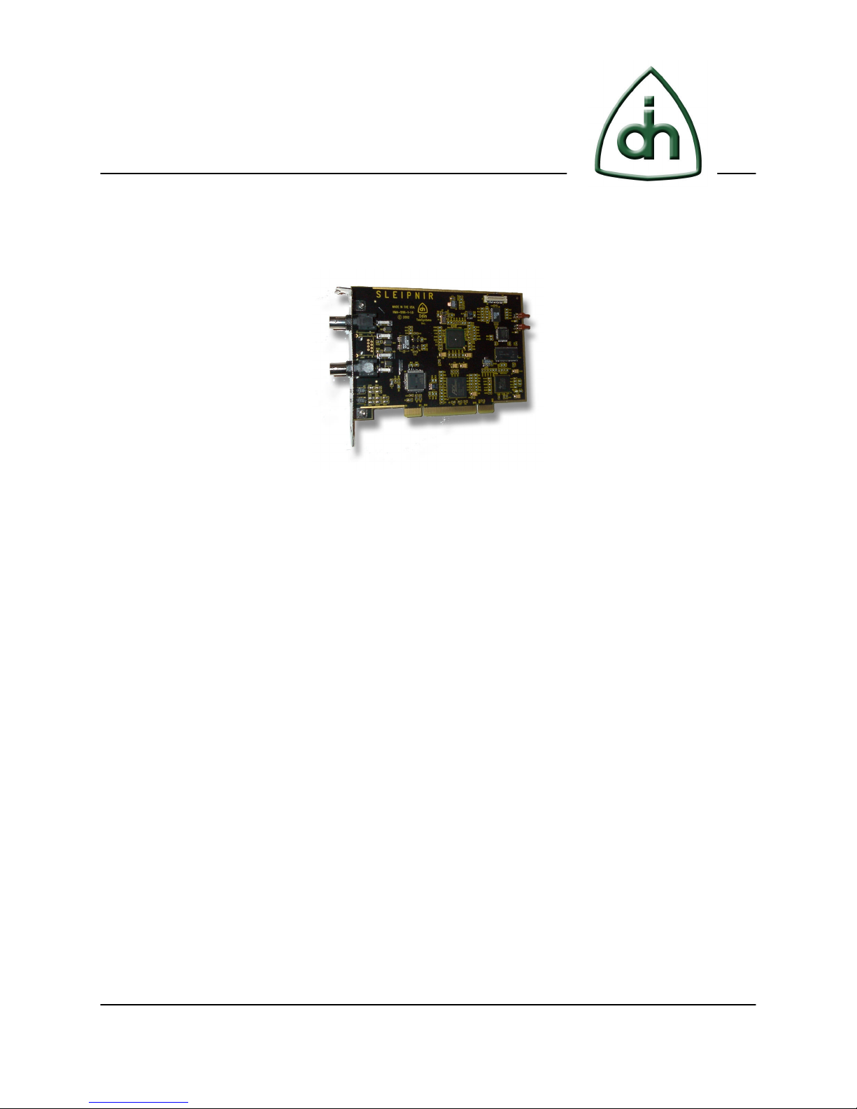
Page 2

Sleipnir-1-PCI Technical Description 2(14)
Copyright
© Copyright 2002, Odin TeleSystems, Inc. All rights reserved. No part of this publication may be reproduced,
stored in a retrieval system, or transmitted in any form or by any means, electronic, mechanical, photocopying,
recording or otherwise, without the prior written consent of Odin TeleSystems Inc., 800 East Campbell Road, Suite
334, Richardson, Texas 75081, U. S. A.
Trademarks
Odin TeleSystems, the Odin Logo, OTX, and Sleipnir are trademarks of Odin TeleSystems Inc., which may be
registered in some jurisdictions. Other trademarks are the property of their respective companies.
Changes
The material in this document is for information only and is subject to change without notice. While reasonable
efforts have been made in the preparation of this document to assure its accuracy, Odin TeleSystems Inc., assumes
no liability resulting from errors or omissions in this document, or from the use of the information contained herein.
Odin TeleSystems Inc. reserves the right to make changes in the product design without reservation and notification
to its users.
Warranties
THE PRODUCT AND ITS DOCUMENTATION ARE PROVIDED “AS IS” AND WITHOUT WARRANTY OF
ANY KIND. ODIN TELESYSTEMS EXPRESSLY DISCLAIMS ALL THE WARRANTIES, EXPRESS OR
IMPLIED, INCLUDING, BUT NOT LIMITED TO THE IMPLIED WARRANTIES OF MERCHANTABILITY
AND FITNESS FOR PARTICULAR PURPOSE. ODIN TELESYSTEMS DOES NOT WARRANT THAT THE
FUNCTIONALITY OF THE PRODUCT WILL MEET ANY REQUIREMENTS, OR THAT THE OPERATIONS
OF THE PRODUCT WILL BE UNINTERRUPTED OR ERROR-FREE, OR THAT DEFECTS WILL BE
CORRECTED. FURTHERMORE, ODIN TELESYSTEMS DOES NOT WARRANT OR MAKE ANY
REPRESENTATIONS REGARDING THE USE OF THE PRODUCT OR ITS DOCUMENTATION IN TERMS
OF THEIR CORRECTNESS, ACCURACY, RELIABILITY, OR OTHERWISE. NO ORAL OR WRITTEN
INFORMATION OR ADVISE GIVEN BY ODIN TELESYSTEMS OR ODIN TELESYSTEMS’ AUTHORIZED
REPRESENTATIVE SHALL CREATE A WARRANTY. SOME JURISDICTIONS DO NOT ALLOW THE
EXCLUSION OF IMPLIED WARRANTIES, SO THE ABOVE EXCLUSION MAY NOT APPLY.
UNDER NO CIRCUMSTANCE SHALL ODIN TELESYSTEMS INC., ITS OFFICERS, EMPLOYEES, OR
AGENTS BE LIABLE FOR ANY INCIDENTAL, SPECIAL, OR CONSEQUENTIAL DAMAGES (INCLUDING
DAMAGES FOR LOSS OF BUSINESS, PROFITS, BUSINESS INTERRUPTION, LOSS OF BUSINESS
INFORMATION) ARISING OUT OF THE USE OR INABILITY TO USE THE PRODUCT AND ITS DOCUMENTATION, EVEN IF ODIN TELESYSTEMS HAS BEEN ADVISED OF THE POSSIBILITY OF SUCH
DAMAGES. IN NO EVENT WILL ODIN TELESYSTEMS’ LIABILITY FOR ANY REASON EXCEED THE
ACTUAL PRICE PAID FOR THE PRODUCT AND ITS DOCUMENTATION. SOME JURISDICTIONS DO
NOT ALLOW THE LIMITATION OR EXCLUSION OF LIABILITY FOR INCIDENTAL AND CONSE-
QUENTIAL DAMAGES, SO THE ABOVE LIMITATION OR EXCLUSION MAY NOT APPLY.
Doc. No. 1111-1-HAA-1051-1 Rev. 1.0-P1
Copyright © Odin TeleSystems Inc., 2002
Page 3

Sleipnir-1-PCI Technical Description 3(14)
Table of Contents
1 Abstract.................................................................................................................................5
2 Sleipnir-1-PCI Overview ......................................................................................................5
3 Physical specifications ..........................................................................................................6
3.1 RJ45 connector option ..........................................................................................................6
3.2 BNC connector option ..........................................................................................................6
4 PCM Highways.....................................................................................................................8
5 API Supported Physical Devices ..........................................................................................9
5.1 Board Devices .......................................................................................................................9
5.2 T1/E1 Line Interface Device.................................................................................................9
5.3 DSP........................................................................................................................................9
6 Line Interface Functionality.................................................................................................9
6.1 Line Configurations..............................................................................................................9
6.2 Fault Monitoring.................................................................................................................10
6.3 Loop Back...........................................................................................................................11
7 PCI Bus ...............................................................................................................................11
8 T1 / E1 Interface Connections............................................................................................12
9 Clocks..................................................................................................................................12
10 JTAG...................................................................................................................................12
11 Indicators ............................................................................................................................13
Doc. No. 1111-1-HAA-1051-1 Rev. 1.0-P1
Copyright © Odin TeleSystems Inc., 2002
Page 4

Sleipnir-1-PCI Technical Description 4(14)
12 Power ..................................................................................................................................13
13 Certifications.......................................................................................................................13
14 Reference documents..........................................................................................................13
15 Glossary ..............................................................................................................................14
Doc. No. 1111-1-HAA-1051-1 Rev. 1.0-P1
Copyright © Odin TeleSystems Inc., 2002
Page 5

Sleipnir-1-PCI Technical Description 5(14)
1 Abstract
This document provides a technical description of Odin TeleSystems’ Sleipnir-1-PCI
adapter card. This presentation is targeted to systems integrators and application
developers who are developing telecommunications systems and/or software applications
using the Sleipnir-1-PCI platform. The purpose of this document is to provide the needed
information about the hardware to allow software developers to efficiently integrate
Sleipnir-1-PCI into their overall system under design.
For information on how to develop host applications utilizing the OTX Hardware Device
Driver Application Programming Interface (API), please refer to the “Programmer’s
Guide for OTX Hardware API” document (Odin TeleSystems Inc. document number
1411-1-SAA-1006-1). For information on how to develop custom DSP applications,
please refer to “Programmer’s Guide for OTX C54x DSP Software Development Kit”
(Odin document number 1412-1-SAA-1007-1). And finally, for help on how to install the
Sleipnir-1-PCI card and the OTX Device Driver Software, please refer to the Installation
Guide for OTX PCMCIA Adapters (Odin TeleSystems Inc. document number 1512-1HCA-1003-1).
2 Sleipnir-1-PCI Overview
Sleipnir-1-PCI is single span T1/E1/J1 adapter for the PCI Local bus. It is available in
two different configurations:
• LAN (Local Area Network) and WAN (Wide Area Network) configuration
• Telecom configuration.
The Sleipnir LAN and WAN configuration is supplied with a network driver and
supporting software to allow high speed PPP and Frame Relay connectivity. No
programming is needed in this configuration.
The Sleipnir telecom configuration is a member of the Odin Telecom frameworX (OTX)
product family. It is supported by the OTX device driver and by the OTX Hardware
Application Programming Interface (API). It is populated with a Texas Instruments
TMS320VC5510 400 Mips DSP and 16MB external memory. Equipped with the
appropriate OTX software modules, Sleipnir-1-PCIcan be utilized in a variety of T1/E1,
Integrated Services Digital Network (ISDN), Frame Relay, and Signaling System #7
(SS#7) applications.
The Sleipnir-1-PCI supports a single T1/J1 or E1 interface at the speeds of 1.544 Mbps
and 2.048 Mbps, respectively. The same board supports both T1/J1 and E1. The Sleipnir1-PCI is available with two different connector options:
Doc. No. 1111-1-HAA-1051-1 Rev. 1.0-P1
Copyright © Odin TeleSystems Inc., 2002
Page 6

Sleipnir-1-PCI Technical Description 6(14)
• RJ45 connector with line terminating impedance of 100 / 120 ohms
• BNC connectors (TX and RX) with line terminating impedance of 75 ohms
Sleipnir-1-PCI supports all popular frame formats and line coding.
3 Physical specifications
Sleipnir-1-PCI is a half-length PCI board available with two different T1/E1/J1 connector
options. The two different connector options are listed in the chapters below.
3.1 RJ45 connector option
The Sleipnir-1-PCI with the RJ45 connector option is shown in the figure below.
Dual color
Status
LED
Dual color
Status
LED
D2
D1
J201
T1/E1
Connector
RJ45
PCI Connector
6.00"
JTAG connector
DSP Emulator Port
J1
External Clock
Input connector
Recovered T1/
E1 clock output
connector
J3
J2
4.20”
3.2 BNC connector option
The Sleipnir-1-PCI with the BNC connector option is shown in the figure below.
Doc. No. 1111-1-HAA-1051-1 Rev. 1.0-P1
Copyright © Odin TeleSystems Inc., 2002
Page 7

Sleipnir-1-PCI Technical Description 7(14)
6.00"
T1/E1 Connector
TX - BNC
JTAG connector
DSP Emulator
J302
T1/E1 Connector
RX - BNC
J301
Port
Recovered T1/E1
External Clock
Input connector
4.20”
clock output
connector
Dual color
Status LED
Dual color
Status LED
D2
D1
1 3
4 Data Architecture
Internally, Sleipnir-1-PCI utilizes serial TDM (Time-Division Multiplexed) data streams
for transfer of data or voice. The internal serial TDM data streams are called “Highways.”
The external interface is referred to as “span”.
The serial highways provide data paths between physical devices as shown in the figure
below.
PCI connector
Doc. No. 1111-1-HAA-1051-1 Rev. 1.0-P1
Copyright © Odin TeleSystems Inc., 2002
Page 8

Sleipnir-1-PCI Technical Description 8(14)
Sleipnir-1-PCI
T1/E1
connector
LIU and
Framer
DMA Burst device
OTX or Sleipnir-1-PCI network driver
Buffering of highway data
User Application
(Sleipnir-1-PCI Telecom configuration only)
Highway
connection
device
DSP
(optional)
Kernel mode
User mode
5 PCM Highways
The Sleipnir-1-PCI utilizes 2 Mbit/sec PCM highways for data routing. When the
optional DSP is installed, the DSP can process data from ether the incoming data stream
Doc. No. 1111-1-HAA-1051-1 Rev. 1.0-P1
Copyright © Odin TeleSystems Inc., 2002
Page 9

Sleipnir-1-PCI Technical Description 9(14)
or from the host by way of DMA transfer. The DSP can supply data to ether the outgoing
data stream or the host by way of DMA transfer.
6 API Supported Physical Devices
6.1 Board Devices
The Sleipnir configuration and status registers are accessible by API calls. The board
devices include the serial to parallel converters and the DMA controller. The application
can read or write the data directly from the Sleipnir buffers, or have the DMA controller
place the data in the host memory and notify the application when data is available.
6.2 T1/E1 Line Interface Device
The Sleipnir Line Interface device fully supported by API calls to configure the interface
for the required functionality. There is full access to all device registers for monitoring or
diagnostics.
6.3 DSP
The optional DSP on the Sleipnir can be used to run Odin provided standard DSP
applications or they can be used to run user developed custom applications. The Sleipnir
telecom configuration is delivered with a number of Odin’s Signal Processing Module
(SPM). These SPMs, or DSP application packages, provides supports for many common
telecom applications; such as tone detection and generation, FSK detection, and HDLC
sending and receiving.
For more information on custom DSP application development, please refer to “Pro-
grammer’s Guide for OTX C54x DSP Software Development Kit” (Odin document
number 1412-1-SAA-1007-1)
7 Line Interface Functionality
7.1 Line Configurations
The Sleipnir-1-PCI line interfaces support several different line codes:
• HDB3 - High Density Bipolar 3
• B8ZS - Bipolar 8 Zero Substitution
Doc. No. 1111-1-HAA-1051-1 Rev. 1.0-P1
Copyright © Odin TeleSystems Inc., 2002
Page 10

Sleipnir-1-PCI Technical Description 10(14)
• AMI - Alternate Mark Inversion
• AMI with NZC
For the T1 operation mode, the following framing formats can be used:
• F4 - 4-frame multiframe
• F12 - 12 frame multiframe (D3/D4, Superframe)
• ESF - Extended Superframe
• F72 - 72 frame multiframe (SLC96 mode)
For the E1 operation mode, Sleipnir-1-PCI supports the following framing formats:
• Doubleframe
• CRC multiframe
7.2 Fault Monitoring
The line interface subsystem supports fault and performance monitoring. The transceiver
subsystem detects and reports the following alarms in the receive streams:
• Framing errors
• Cyclic Redundancy Check (CRC) errors
• Code violations
• Loss of frame alignment
• Loss of Signal (LOS)
• Alarm Indication Signal (AIS)
• E bit errors (E1 only)
• Slip
• Remote Alarm Indication (RAI, Yellow Alarm)
The line interface subsystems also supports the transmitting of the following alarms
towards the remote end:
Doc. No. 1111-1-HAA-1051-1 Rev. 1.0-P1
Copyright © Odin TeleSystems Inc., 2002
Page 11

Sleipnir-1-PCI Technical Description 11(14)
• Alarm Indication Signal (AIS)
• Remote Alarm Indication (RAI, Yellow alarm)
• Auxiliary Pattern (AUXP)
7.3 Loop Back
The line interface subsystem implements a remote loop back for line testing. In the
remote loop back mode, the clock and data recovered from the line inputs are routed back
to the line outputs through the analog transmitter.
8 Testing features
The Sleipnir Telecom configuration offers a variety of features to facilitate low-level
T1/E1/J1 testing:
• Full access to F, Y, Si, and Sa bits in E1 mode
• Full access to FS/DL-bits in T1 mode (including support for the DL-channel
protocol according to T1.403-1989 ANSI or to AT&T TR54016 specification)
• Programmable line build-out in T1/J1 mode
• Transparent mode
• Programmable transmit pulse shape and receive input threshold
• Insertion and detection of single alarms (e.g. Code Violation, Framing Errors,
etc)
• Support for generation and detection of Loop codes
• Support for channel loopback
• Support for PRBS (BERT patterns)
9 PCI Bus
The Sleipnir-1-PCI board is compliant with the PCI 2.1 local bus specification. It is a
universal interface, supporting both 3.3 volt and 5 volt signaling. The Sleipnir-1-PCI
supports 32 bits at 33 MHz and can be both Slave and Master.
Doc. No. 1111-1-HAA-1051-1 Rev. 1.0-P1
Copyright © Odin TeleSystems Inc., 2002
Page 12

RJ-45
Sleipnir-1-PCI Technical Description 12(14)
10 T1 / E1 Interface Connections
The back panel of Sleipnir-1-PCI contains ether a RJ45 connector or two BNC
connectors. The RJ45 connector provides balanced 100 / 120 ohm transmit and receive
connection, while the BNC connectors provide unbalanced 75 ohm connections.
Position #
1
Receive (RX) Line 1 (Tip)
2
Receive (RX) Line 2 (Ring)
3
4
Transmit (TX) Line 1 (Tip)
5
Transmit (TX) Line 2 (Ring)
6
7
8
Position 1
11 Clocks
12 JTAG
On the Sleipnir-1-PCI board, all the internal TDM data highways and the all the devices
processing TDM data are synchronized to one clock reference. The clock reference can
be derived from multiple sources and then routed to all the devices. The following clocking sources are supported by Sleipnir-1-PCI:
• Clock extracted from the incoming T1/E1/J1 span
• External 2.048 kHz clock (J3 connector)
• On-board free running oscillator
The J2 connector can be used to output the Sleipnir-1-PCI clock reference to another
device or equipment.
The JTAG port (reference designator J1) are used for Board Testing, programming of
The FPGA PROMS, and Connecting the DSP emulator board for DSP Software
Development.
Table x. JTAG Chains
Chain Parts
TMS0 PROM
Doc. No. 1111-1-HAA-1051-1 Rev. 1.0-P1
Copyright © Odin TeleSystems Inc., 2002
Page 13

Sleipnir-1-PCI Technical Description 13(14)
TMS1 LIU, PCI
TMS2 FPGA
TMS3 DSP
13 Indicators
The Sleipnir-1-PCI has four dual color LED indicators:
• Loss of signal / Activity
• Framing Error
• Alarm
• Auxiliary
The Auxiliary LED is driven from the (optional) DSP and can be configured arbitrarily.
14 Power
The Sleipnir-1-PCI operates from 3.3 Volt power supplied from the host PC. Power
consumption is TBD.
15 Certifications
Final certifications are TBD. The following is a list of planned certifications:
• FCC Part 15 (CFR47, Part 15, Subpart B)
• FCC Part 68
• CE EMC (EN61326-1 Class B Equipment, AS/NZS 2064 Class B Limits)
• Safety EN60950 and UL60950
16 Reference documents
The following documents provide further detailed information related to the Sleipnir-1PCI board:
Doc. No. 1111-1-HAA-1051-1 Rev. 1.0-P1
Copyright © Odin TeleSystems Inc., 2002
Page 14

Sleipnir-1-PCI Technical Description 14(14)
• Programme r’s Guide for OTX Hardware Driver (Odin document # 1412-1-SAA-
1006-1)
• Installation Guide for OTX PCI Adapters (Odin document number 1512-1-
HCA-1001-1)
• Programmer’s Guide for OTX C54x DSP Software Development Kit (Odin
document number 1412-1-SAA-1007-1)
17 Glossary
OTX – Odin Telecom FrameworX
DSP – Digital Signal Processor (optional device on Sleipnir-1-PCI)
SDK – Software Development Kit (supplied with the Sleipnir Telecom configuration)
API – Application Programmer Interface
CPU – Central Processing Unit. Refers to the host PC in this document.
EEPROM – Electrically Erasable Programmable Read Only Memory.
FPGA – Field Programmable Gate Array.
LED – Light Emitting Diode
LS – Least Significant
MS – Most Significant
Doc. No. 1111-1-HAA-1051-1 Rev. 1.0-P1
Copyright © Odin TeleSystems Inc., 2002
 Loading...