

OCULAR GDM12864A User Manual

User’s Guide
GDM12864A
™
LCM
(Liquid Crystal Display Module)
XIAMEN OCULAR LCD DEVICES CO., LTD.
??????????????
South 5F., Guang Xia Bldg. Torch Hi-tech
Develop. Area, Xiamen, China 361006
Tel: (0592)6026045 Fax: (0592)6026021

GDM12864A LCM Use’s Guide
Contents
Chapter 1. Introduction to ITM-12864A LCM
1
Features 1
Mechanical Specifications 1
Temperature Characteristics 1
External Dimensions 2
Application Diagram 3
Electro- Optical characteristics 4
Interface Pin Connections 5
Electrical Absolute Maximum Rating (KS0107B) 6
DC Electrical Characteristics (KS0107B) 6
Electrical Absolute Maximum Rating (KS0108B) 7
DC Electrical Characteristics (KS0108B) 7
Chapter 2. Driver IC (KS0107B) Function Description 8
Introduction 8
AC Characteristics 9
Master Mode 9
Slave Mode 10
Functional Description 11
RC Oscillator 11
Timing Generation Circuit 11
Data Shift & Phase Select Control 12
Chapter 3. Driver IC (KS0108B) Function Description 13
Introduction 13
AC Characteristics 13
Operating Principles & Methods 16
Display Control Instruction 19

Chapter 1 Introduction to GDM12864A LCM 1
CHAPTER 1
Introduction to ITM-12864A LCM
ITM-12864A is a dot matrix graphic LCD module which is fabricated by low power COMS
technology. It can display 128*64 dots size LCD panel using a 128*64 bit-mapped Display Data
RAM (DDRAM). It interfaces with an 8-bit microprocessor.
Features
?? Display format: 128*64 dots matrix graphic
?? STN yellow-green mode
?? Easy interface with 8-bit MPU
?? Low power consumption
?? LED back-light
?? Viewing angle: 6 O’clock
?? Driving method : 1/64 duty , 1/6.7 bias
?? LCD driver IC: KS0108B(2 ?)? KS0107B
?? Connector: Zebra
Mechanical Specifications
Item Dimension Unit
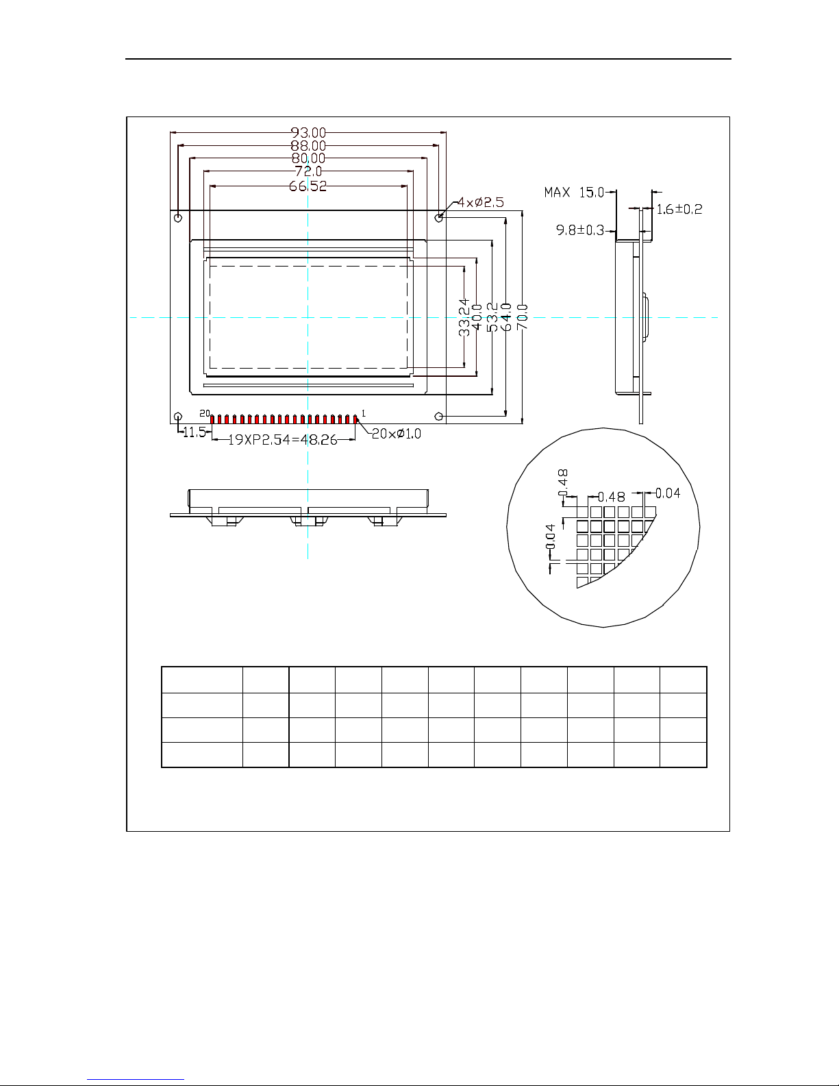
Module Size(W*H*T) 93.0*70.0*10.0 mm
Viewing Area(W*H) 72.0*40.0 mm
Number of Dots 128.0*64.0 PCS
Dot Size(W*H) 0.48*0.48 mm
Dot Pitch(W*H) 0.52*0.52 mm
Module Size With B/L 93.0*70.0*15.0 mm
Temperature Characteristics
Parameter Symbol Rating Unit
Operating temperature Topr 0 ~ +50
?
Storage temperature Tstg -20 ~ +70
?
Chapter 1 Introduction to GDM12864A LCM 2
Figure 1. External Dimensions
PIN 1 2 3 4 5 6 7 8 9 10
SIGNAL Vss VDD V0 D/I R/W E DB0 DB1 DB2 DB3
PIN 11 12 13 14 15 16 17 18 19 20
SIGNAL DB4 DB5 DB6 DB7 CS1 CS2 RES VEE A K
*NOTE: 1.All units are mm.
2.Tolerances unless otherwise specified ?0.2.
INTECH LCD MODULE ITM-12864A
Chapter 1 Introduction to GDM12864A LCM 3
Figure 2. Application Diagram
CS2B
DB[0:7]
RESETB
CS1B
S64
S1
CS3
RSERW
12
V3
KS0108B
(Bottom view)
VSS
VSS
VEEV4V5
CLK1
CL2
CLK2
M
FRM
V0
V1
V2
VDD
ADC
VEE
SEG64
DB[0:7]
RESETB
CS1B
CS3
CS2B
RESETB
DB[0:7]
CS2
CS1
E
RW
RS
12
RS
RW
E
SEG1
....
C1C64 CCRR
ADC
VEE
VSS
V3
MPU
VSS
V5
V4V0V2
V1
VDD
S1 S64
KS0108B
(Bottom view)
CLK2
CL2
FRM
CLK1
M
VSS
V4V3V5
V1V0V2
VEE
V4
V5
V2
V3
VDD
V0
V1
FS
DS1
VSS
DS2
MS
PCLK2
VDD
SHL
CL2
CLK2
CLK1
FRM
M
KS0107B
SEG128
LCD panel
(128X64)
SEG65
....
. .
COM64
COM1
*Note
1/64 duty, 1/6.7 bias
VDD>V1>V2>V3>V4>V5>VEE
Chapter 1 Introduction to GDM12864A LCM 4
Electro-Optical characteristics
TN Type (Twisted Nematic )
Item Symbol Min. Typ. Max. Unit Condition Note
?2 -?1
Viewing Angle
f
40 - - deg. Cr = 2.0 1,2
Contrast Ratio Cr - 4 - -
?=20
?
f = 0?
3
Response Time (rise) tR - 110 - ms
?=20
?
f = 0?
4
Response Time (fall) tF - 110 - ms
?=20
?
f = 0?
4
STN Type (Super Twisted Nematic )
Item Symbol Min. Typ. Max. Unit Condition Note
?2 -?1
Viewing Angle
f
70
-90
- +90 deg. Cr = 2.0 1,2
Contrast Ratio Cr - 4 - -
?=20
?
f = 0?
3
Response Time (rise) tR - 110 - ms
?=20
?
f = 0?
4
Response Time (fall) tF - 110 - ms
?=20
?
f = 0?
4
4. Definition of optical response
3. Definition of contrast Cr
2. Definition of viewing angle
¦È
1
&
¦Õ
2
1. Definition of angle ¦È&
¦Õ
¦È
¦È
Y
(¦Õ=18
0¦Ï)Y’
(¦Õ=
0¦Ï)¦È<20¦Ï<
¦È
¦È
20
¦Ï
¦È
2
2.0
C
r
100%
100%
100%
Intensity
Intensity
0%
B
A
Off
Off
On
90%
10%
t
F
t
R
Time
Driving Voltage
Set Point
Cr = ( A / B )
p
Negative : P = -1
Positive : P = +1
Non-
Selected
Dots
Dots
selected

Chapter 1 Introduction to GDM12864A LCM 5
Interface Pin Connections
Pin
No.
Symbol I/O Type Description
1 VSS Supply Ground
2 VDD Supply Power supply
3 V0 Supply
LCD driver supply voltage
4 D/I Data input/output pin of internal shift register
MS SHL DIO1 DIO2
H H Output Output
H L Output Output
L H Input Output
L L Output Input
5 R/W Read or Write
RW Description
H Data appears at DB[7:0] and can be read by the CPU while
E= H CS1B=L,CS2B=L and CS3=H.
L Display data DB[7:0] can be written at falling edge of E
when CS1B=L, CS2B=L and CS3=H.
6 E Enable signal
E Description
H Read data in DB[7:0] appears while E= “High”.
L Display data DB[7:0] is latched at falling edge of E.
7 DB0
8 DB1
9 DB2
10 DB3
11 DB4
12 DB5
13 DB6
14 DB7
I/O Data bus [0~7]
Bi-directional data bus
15
16
CS1
CS2
I Chip selection
When CS1=H,CS2=L, select IC1
When CS1=L,CS2=H, select IC2
17 RESETB I Reset signal.
When RSTB=L
?1?ON/OFF register becomes set by 0.(display off)
?2?display start line register becomes set by 0 (Z-address 0 set, display
from line 0)
?3?After releasing reset , this condition can be changed only by
instruction.
18 VEE Power
VEE is connected by the same voltage.
19 A
Back-light anode
20 K
Back-light cathode
 Loading...