


HIPPO DCA 1
486

The material in this manual is for information only and is subject to change without
notice.
REVISION: 1.01
TRADEMARKS
All tradmarks mentional in this manual are registered property of the repective owners.

RADIO FREQUENCY INTERFERENCE STATEMENT
This equipment generates and uses radio frequency energy and if
not installed and used properly, that is, in strict accordance with
the manufacturer's instructions, may cause interference with
radio and television reception.
If this equipment does cause interference to radio or TV
reception, which can be determined by turning the equipment off
and on, the user is encouraged to try to correct the interference
by one or more of the following measures:
* Reorient the receiving antenna.
* Relocate the computer away from the receiver.
* Move the computer away from the receiver.
* Plug the computer into a different outlet so that computer and
receiver are on different branch circuits.
* Ensure that card slot covers are in place when no card is
installed.
* Ensure that card mounting screws, attachment connector
screws, and ground wires are tightly secured.
* If peripherals are used with this system, it is suggested to use
shielded, grounded cables, with in-line filters if necessary.
If necessary, the user should consult the dealer service
representative for additional suggestions.
The manufacturer is not responsible for any radio or TV
interference caused by unauthorized modifications to this
equipment. It is the responsibility of the user to correct such
interference.

NOTE
1. Electronic components are sensitive to dust and dirt. Do
inspect and clean the computer system regularly.
2. Turn off the power whenever you install or remove any
connector, memory module and add-on card. Before
turning on the power, make sure that all the connectors,
memory modules and add-on cards are secured.
3. After power is on, wait for a minute. The system BIOS
are going through a self-test during this period and
nothing is shown on the screen. After the self-test, the
system BIOS will initialize the display adaptor and show
messages.
4. The SIMM sockets are fragile device. Do not force the
SIMM modules into the sockets. It may break the locking
latches.

Table of Content
Chapter One GENERAL FEATURES
Specification............................................................... 1-1
Dynamic Cache Architecture (DCA) ......................... 1-2
Chapter Two CONFIGURING THE SYSTEM
Installing Processor .................................................... 2-1
Installing RAM Modules ........................................... 2-2
Configuration of Memory .......................................... 2-3
DRAM Configuration ................................................ 2-3
Control of System Speed ........................................... 2-4
Reset CMOS Setup Information ................................ 2-4
System Board Jumper Setting .................................... 2-5
System Board Connectors .......................................... 2-6
Chapter Three TECHNICAL INFORMATION
Memory Mapping ...................................................... 3-1
I/O Address Map ........................................................ 3-2
System Interrupts ....................................................... 3-4
Direct Memory Access (DMA).................................. 3-5
System Expansion Bus............................................... 3-6

Appendix A OPERATION AND MAINTENANCE
Static Electricity ........................................................ A-1
Keeping The System Cool ........................................ A-1
Cleaning The “Golden Finger” ................................. A-2
Cleaning The Motherboard ....................................... A-2
Appendix B TROUBLESHOOTING
Main Memory Error ...................................................B-1
Appendix C SUMMERY OF JUMPER SETTING
Appendix D SYSTEM BOARD LAYOUT

Chapter ONE
1-1
Chapter One
General Features
SPECIFICATION
Processor : 80486DX4, 80486DX2, 80486DX or
80486SX,CX486DX, CX486DX2
Speed : Turbo/normal speed
I/O Slot : Compatible to standard AT bus
Six 16-bit slots Three VESA VL-BUS slots
Cache : 8KB four way set associative internal cache
Memory : 4 level deep write buffer with byte gathering
Shadow RAM for system and video BIOS
Page mode and hidden refresh
4pcs of 72 pin SIMM modules

Chapter ONE
1-2
System Support
Functions : - 8-Channel DMA (Direct Memory Access)
- 16-level interrupt
- 3 programmable timers
- CMOS RAM for system configuration
- Real time clock with battery back-up
- Fast A20 gate and fast reset
Other Features : - On board POWERGOOD generation
- External battery connector
DYNAMIC CACHE ARCHITECTURE (DCA)
DCA (dynamic Cache Architecture) is a new Cache Memory DCA
literally boosts the cache memory efficiency by as much as 300
percent over conventional external cache! It is integrated as part of
the high speed logic of the motherboard.
DCA, it's Byte Gathering Write Buffers collect 8 and 16 bit
"packets" of information until a single 32 bit "packet" is formed.
Using Burst Mode, it then "Writes" this single informational
"string" back to RAM in one operation, rather than in several time
consuming ones. This is a tremendous improvement on the
efficiency of data transfer, as the information is handled solely
through the CPU, the High Speed Chipset and the lightning fast
Internal Cache of the 80486.
Chapter TWO
2-1
Chapter Two
Configuring The System
Important Note : Turn off the power before installing or replacing any
component.
Warning : Make sure the following jumpers setting in a right position. Wrong
setting will burn out the CPU.
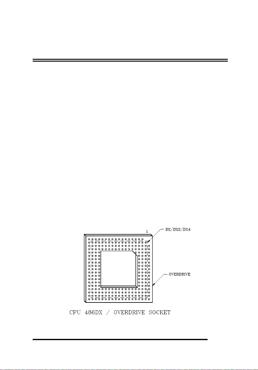
INSTALLING PROCESSOR (DX, SX, DX2, DX4)
Processor 486DX/DX2/DX4/P24T overdrive is a PGA devices.
There is a 238-pin PGA socket or ZIP socket. To install processor,
be sure to line up pin 1 of the CPU with pin 1 of the socket as
shown below. Make sure that the processor is firmly inserted into
the socket.

Chapter TWO
2-2
For DX, SX, DX2 are 5V supply voltage. Due to the DX4 is
3.45V supply voltage, a sohisticated on board auto detect voltage
regulator is implemented on OCTEK HIPPO DCA 1. Therefore,
it’s no need to add any jumpers for different CPU.
INSTALLING RAM MODULES
OCTEK HIPPO DCA 1 has four sockets on board for 72pin
SIMM modules. The modules should be locked by the sockets.
Please check carefully before turning on the power. Otherwise,
the system will not work properly.
To install a module, the module edge is angled into the socket's
contact and then the module is pivoted into position, where the
locking latches will secure it. If the module edge is not completely
inserted into the socket, it cannot be pivoted to be in vertical
position and should be dragged out and re-inserted again. Do not
force the module into the SIMM socket. It will damage the locking
latches.

Chapter TWO
2-3
CONFIGURATION OF MEMORY
There are several combinations of DRAM types you may consider.
1Mx32 or 4Mx32 SIMM are acceptable. The memory size is
detected automatically by system BIOS and indicated during
memory test after reset. No jumper is needed to be set for the
memory size and DRAM type.
DRAM CONFIGURATION
SM1
SM2
SM3
SM4
TOTAL
1Mx32 4M
1Mx32
1Mx32
8M
1Mx32
1Mx32
1Mx32
12M
1Mx32
1Mx32
1Mx32
1Mx32
16M
4Mx32 16M
1Mx32
4Mx32
20M
1Mx32
1Mx32
4Mx32
24M
1Mx32
1Mx32
1Mx32
4Mx32
28M
4Mx32
4Mx32
32M
1Mx32
4Mx32
4Mx32
36M
1Mx32
1Mx32
4Mx32
4Mx32
40M
4Mx32
4Mx32
4Mx32
48M
1Mx32
4Mx32
4Mx32
4Mx32
52M
4Mx32
4Mx32
4Mx32
4Mx32
64M

Chapter TWO
2-4
CONTROL OF SYSTEM SPEED
System speed can be controlled by keyboard and turbo switch. To
change the speed by keyboard, use `-' and `+' of the numeric
keypad. Press `Ctrl' `Alt' and `-' for slow speed and press `Ctrl'
`Alt' and `+' for fast speed.
Connect P1 to the turbo switch of the case and P5 to the turbo LED
of the case. When the turbo mode is selected, the turbo LED of
the case will be turned on.
Whenever the system speed is set to be slow by turbo switch, it
cannot be changed by the keyboard, and vice versa.
RESET CMOS SETUP INFORMATION
Sometimes, the improper setting of system setup may make the
system malfunction. In this case, turn off the power and set JP10
to 2-3 for a while. The internal CMOS status register is reset.
Then set the jumper to 1-2 of JP10 and turn on the power. The
BIOS finds the CMOS status register is reset and regards the setup
information is invalid. So it will prompt you to correct the
information.

Chapter TWO
2-5
SYSTEM BOARD JUMPER SETTING
There are several options which allows user to select by hardware switches.
Display Selection
JP7
1-2
CGA, EGA, VGA
2-3
Monochrome display *
CPU Type
486DX\DX2
\DX4
486SX
487SX
JP6
1 - 2
2 - 3
1 - 2
JP8
2 - 3
NO
1 - 2
JP9
2 - 3
1 - 2
2 - 3
System Speed (Only for clock chip version)
33MHz
25MHz
JP4
1 - 2
2 - 3
JP5
1 - 2
2 - 3

Chapter TWO
2-6
CPU Clock Multiple (Only for DX4 CPU)
JP17
1-2
Internal Clock 3X
3-4
Internal Clock 2X
5-6
Internal CLock 2.5X
SYSTEM BOARD CONNECTORS
Under typical conditions, these connectors should be connected to
the indicators and switches of the system unit. The functions of
connectors on the motherboard are listed below.
Description
P1
Turbo switch
P2
Speaker connector
P3
Hardware reset connector
P4
Power LED & Ext-lock connector
P5
Turbo LED
P6,P7
Power supply connector
P8
External battery connector
P9
Cooling fan connector
KB1
Keyboard connector
Pin assignment of the connector are illustrated as follows:
P1 - Turbo Switch Connector
Pin
Assignment
1
Selection Pin
2
Ground

Chapter TWO
2-7
P2 - Speaker Connector
Pin
Assignment
1
Data out
2
+5 Vdc
3
Ground
4
+5 Vdc
P3 - Hardware Reset Connector
Pin
Assignment
1
Selection Pin
2
Ground
P4 - Power LED & Ext-Lock Connector
Pin
Assignment
1
+5 Vdc
2
Key
3
Ground
4
Keyboard inhibit
5
Ground
P5 - Turbo LED Connector
Pin
Assignment
1
+5Vdc
2
LED signal

Chapter TWO
2-8
P6,P7 - Power Supply Connector
Pin
Assignment
1
POWERGOOD
2
+5 Vdc
3
+12 Vdc
4
-12 Vdc
5
Ground
6
Ground
Pin
Assignment
1
Ground
2
Ground
3
-5 Vdc
4
+5 Vdc
5
+5 Vdc
6
+5 Vdc
P8 - External Battery Connector
Pin
Assignment
1
+ Vdc
2
not used
3
Ground
4
Ground
P9 - Cooling Fan Connector
Pin
Assignment
1
+ 5Vdc
2
Ground

Chapter TWO
2-9
KB1 - Keyboard Connector
Pin
Assignment
1
Keyboard clock
2
Keyboard data
3
Spare
4
Ground
5
+5 Vdc

Chapter TWO
2-10
THIS PAGE IS INTENTIONALLY LEFT BLANK
Chapter THREE
3-1
Chapter Three
Technical Information
This section provides technical information about OCTEK HIPPO
DCA 1 and is intended for advanced users interested in the basic
design and operation of OCTEK HIPPO DCA 1.
MEMORY MAPPING
Address
Range
Function
000000-
7FFFFF
000K-512K
System Board Memory
(512K)
080000-
09FFFF
512K-640K
System Board Memory
(128K)
0A0000-
0BFFFF
640K-768K
Display Buffer (128K)
0C0000-
0DFFFF
768K-896K
Adaptor ROM / Shadow RAM
(128K)
0E0000-
0EFFFF
896K-960K
System ROM / Shadow
RAM (64K)
0F0000-
0FFFFF
960K-1024K
System BIOS ROM / Shadow
RAM (64K)
100000-
7FFFFF
1024K-
8192K
System Memory
800000-
FFFFFF
8192K-
16318K
System Memory

Chapter THREE
3-2
I/O ADDRESS MAP
I/O Address Map on System Board
I/O address hex 000 to 0FF are reserved for the system board I/O.
ADDRESS
(HEX)
DEVICE
000-01F
DMA Controller 1, 8237
020-03F
Interrupt Controller 1, 8259, Master
040-05F
Timer, 8254
060-06F
Keyboard Controller
070-07F
Real Time Clock, NMI
(non-maskable interrupt) mask
080-09F
DMA Page Register, 74LS612
0A0-0BF
Interrupt Controller 2, 8259
0C0-0DF
DMA Controller 2, 8237
0F0
Clear Math Coprocessor Busy
0F1
Reset Math Coprocessor
0F8-0FF
Math Coprocessor Port

Chapter THREE
3-3
I/O address hex 100 to 3FF are available on the I/O channel.
ADDRESS
(HEX)
DEVICE
1F0-1F8
Fixed Disk
200-207
Game I/O
278-27F
Parallel Printer Port 2
2F8-2FF
Serial Port 2
300-31F
Prototype Card
360-36F
Reserved
378-37F
Parallel Printer Port 1
380-38F
SDLC, bisynchronous 2
3A0-3AF
Bisynchronous 1
3B0-3BF
Monochrome Display and Printer Adapter
3C0-3CF
Reserved
3D0-3DF
Color Graphics Monitor Adapter
3F0-3F7
Diskette Controller
3F8-3FF
Serial Port 1
Chapter THREE
3-4
SYSTEM INTERRUPTS
Sixteen levels of system interrupts are provided on
OCTEK HIPPO DCA 1. The following shows the interrupt-level
assignments in decreasing priority.
Level Function
Microprocessor NMI Parity or I/O Channel
Check
Interrupt Controllers
CTLR 1 CTLR 2
IRQ0 Timer Output 0
IRQ1 Keyboard
IRQ2
IRQ8 Real-time Clock Interrupt
IRQ9 Software Redirected to
INT 0AH (IRQ2)
IRQ10 Reserved
IRQ11 Reserved
IRQ12 Reserved
IRQ13 Coprocessor
IRQ14 Fixed Disk Controller
IRQ15 Reserved
IRQ3 Serial Port 2
IRQ4 Serial Port 1
IRQ5 Parallel Port 2
IRQ6 Diskette Controller
IRQ7 Parallel Port 1
Chapter THREE
3-5
DIRECT MEMORY ACCESS (DMA)
OCTEK HIPPO DCA 1 supports seven DMA channels.
Channel
Function
0
Spare (8 bit transfer)
1
SDLC (8 bit transfer)
2
Floppy Disk (8 bit transfer)
3
Spare (8 bit transfer)
4
Cascade for DMA Controller 1
5
Spare (16 bit transfer)
6
Spare (16 bit transfer)
7
Spare (16 bit transfer)

Chapter THREE
3-6
SYSTEM EXPANSION BUS
OCTEK HIPPO DCA 1 provides six 16-bit slots and three VL-bus
slots.
The I/O channel supports:
* I/O address space from hex 100 to hex 3FF
* Selection of data access (either 8 or 16 bit)
* 24 bit memory addresses (16MB)
* Interrupts
* DMA channels
* Memory refresh signal
Chapter THREE
3-7
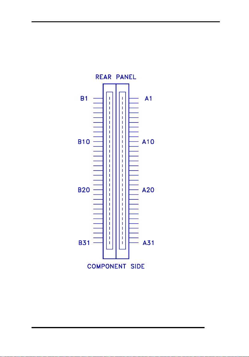
The following figure shows the pin numbering for I/O channel
connectors (A-side and B-side).

Chapter THREE
3-8
The following figure shows the pin numbering for I/O channel
connectors (C-side and D-side).

Chapter THREE
3-9
The following tables summarize pin assignments for the I/O
channel connectors.
I/O Channel (A-Side)
I/O Pin
Signal Name
I/O
A1
-I/O CH CK
I
A2
SD7
I/O
A3
SD6
I/O
A4
SD5
I/O
A5
SD4
I/O
A6
SD3
I/O
A7
SD2
I/O
A8
SD1
I/O
A9
SD0
I/O
A10
-I/O CH RDY
I
A11
AEN
O
A12
SA19
I/O
A13
SA18
I/O
A14
SA17
I/O
A15
SA16
I/O
A16
SA15
I/O
A17
SA14
I/O
A18
SA13
I/O
A19
SA12
I/O
A20
SA11
I/O
A21
SA10
I/O
A22
SA9
I/O
A23
SA8
I/O
A24
SA7
I/O
A25
SA6
I/O
A26
SA5
I/O
A27
SA4
I/O
A28
SA3
I/O
A29
SA2
I/O
A30
SA1
I/O
A31
SA0
I/O

Chapter THREE
3-10
I/O Channel (B-Side)
I/O Pin
Signal Name
I/O
B1
GND
Ground
B2
RESET DRV
I
B3
+5 Vdc
Power
B4
IRQ9
I
B5
-5 Vdc
Power
B6
DRQ2
I
B7
-12 Vdc
Power
B8
0WS
I
B9
+12 Vdc
Power
B10
GND
Ground
B11
-SMEMW
O
B12
-SMEMR
O
B13
-IOW
I/O
B14
-IOR
I/O
B15
-DACK3
I
B16
DRQ3
O
B17
-DACK1
I
B18
DRQ1
O
B19
-Refresh
I/O
B20
CLK
O
B21
IRQ7
I
B22
IRQ6
I
B23
IRQ5
I
B24
IRQ4
I
B25
IRQ3
I
B26
-DACK2
O
B27
T/C
O
B28
BALE
O
B29
+5 Vdc
Power
B30
OSC
O
B31
GND
Ground

Chapter THREE
3-11
I/O Channel (C-Side)
I/O Pin
Signal Name
I/O
C1
SBHE
I/O
C2
LA23
I/O
C3
LA22
I/O
C4
LA21
I/O
C5
LA20
I/O
C6
LA19
I/O
C7
LA18
I/O
C8
LA17
I/O
C9
-MEMR
I/O
C10
-MEMW
I/O
C11
SD8
I/O
C12
SD9
I/O
C13
SD10
I/O
C14
SD11
I/O
C15
SD12
I/O
C16
SD13
I/O
C17
SD14
I/O
C18
SD15
I/O

Chapter THREE
3-12
I/O Channel (D-Side)
I/O Pin
Signal Name
I/O
D1
-MEM CS16
I
D2
-I/O CS16
I
D3
IRQ10
I
D4
IRQ11
I
D5
IRQ12
I
D6
IRQ15
I
D7
IRQ14
I
D8
-DACK0
O
D9
DRQ0
I
D10
-DACK5
O
D11
DRQ5
I
D12
-DACK6
O
D13
DRQ6
I
D14
-DACK7
O
D15
DRQ7
I
D16
+5 Vdc
Power
D17
-MASTER
I
D18
GND
Ground

Chapter THREE
3-13
The following table summery pin assignments for VESA VL-bus
connector.
VL-bus (side A)
I/O Pin
Signal Name
A1
CD1
A2
CD3
A3
GROUND
A4
CD5
A5
CD7
A6
CD9
A7
CD11
A8
CD13
A9
CD15
A10
GROUND
A11
CD17
A12
POWER
A13
CD19
A14
CD21
A15
CD23
A16
CD25
A17
GROUND
A18
CD27
A19
CD29
A20
CD31
A21
CA30
A22
CA28
A23
CD26
A24
GROUND
A25
CA24
A26
CA22
A27
POWER
A28
CA20

Chapter THREE
3-14
VL-bus (side A)
I/O Pin
Signal Name
A29
CA18
A30
CA16
A31
CA14
A32
CA12
A33
CA10
A34
CA8
A35
GROUND
A36
CA6
A37
CA4
A38
WBACK-
A39
BEO-
A40
POWER
A41
BE1-
A42
BE2-
A43
GROUND
A44
BE3-
A45
ADS-
A46
LRDY-
A47
LDEV-
A48
LREQ-
A49
GROUND
A50
LGNT-
A51
POWER
A52
ID2
A53
ID3
A54
ID4
A55
LKEN-
A56
LEADS-

Chapter THREE
3-15
VL-bus (side B)
I/O Pin
Signal Name
B1
CD0
B2
CD2
B3
CD4
B4
CD6
B5
CD8
B6
GROUND
B7
CD10
B8
CD12
B9
POWER
B10
CD14
B11
CD16
B12
CD18
B13
CD20
B14
GROUND
B15
CD22
B16
CD24
B17
CD26
B18
CD28
B19
CD30
B20
POWER
B21
CA31
B22
GROUND
B23
CA29
B24
CA27
B25
CA25
B26
CA23
B27
CA21
B28
CA19

Chapter THREE
3-16
VL-bus (side B)
I/O Pin
Signal Name
B29
GROUND
B30
CA17
B31
CA15
B32
POWER
B33
CA13
B34
CA11
B35
CA9
B36
CA7
B37
CA5
B38
GROUND
B39
CA3
B40
CA2
B41
n/c
B42
RESET-
B43
D/C-
B44
M/IO-
B45
W/R-
B46
RDY-
B47
GROUND
B48
IRQ9
B49
BRDY-
B50
BLAST-
B51
ID0
B52
ID1
B53
GROUND
B54
VLCLK
B55
POWER
B56
LBS16-

Appendix A
A-1
Appendix A
Operation and Maintenance
STATIC ELECTRICITY
When installing or removing any add-on card, DRAM module or
coprocessor, you should discharge the static electricity on your
body. Static electricity is dangerous to electronic device and can
build-up on your body. When you touch the add-on card or
motherboard, it is likely to damage the device. To discharge the
static electricity, touch the metal of your computer. When
handling the add-on card, don't contact the components on the
cards or their "golden finger". Hold the cards by their edges.
KEEPING THE SYSTEM COOL
The motherboard contains many high-speed components and they
will generate heat during operation. Other add-on cards and hard
disk drive can also produce a lot of heat. The temperature inside
the computer system may be very high. In order to keep the system
running stably, the temperature must be kept at a low level. A easy
way to do this is to keep the cool air circulating inside the case.
The power supply contains a fan to blow air out of the case. If you
find that the temperature is still very high, it would be better to
install another fan inside the case. Using a larger case is
recommended if there are a number of add-on cards and disk
drives in the system.

Appendix A
A-2
CLEANING THE "GOLDEN FINGER"
Whenever inserting an add-on card to the motherboard, make sure
that there is no dirt on the "golden finger" of the add-on card. If
not, the contact between the "golden finger" and the slot may be
poor and thus the add-on card may not work properly. Use a pencil
eraser to clean the "golden finger" if dirt is found.
CLEANING THE MOTHERBOARD
The computer system should be kept clean. Dust and dirt is
harmful to electronic devices. To prevent dust from accumulating
on the mother-board, installing all mounting plates on the rear of
the case. Regularly examine your system, and if necessary,
vacuum the interior of the system with a miniature vacuum.

Appendix B
B-1
Appendix B
Troubleshooting
MAIN MEMORY ERROR
After power up, the monitor remains blank, and there are beep
sounds indicating a main memory failure. In this case, turn off the
power and remove all SIMM modules. Carefully place the
modules back to the sockets and make sure that all the modules are
locked by the locking latches firmly.
In some other cases, the total memory found by the BIOS is
different from the actual amount of memory on board. ( Note that
128K bytes memory is reserved for the shadow RAM function and
will not be counted by the BIOS). It is also a memory failure and
you can follow the instruction above.

Appendix B
B-2
THIS PAGE IS INTENTIONALLY LEFT BLANK

Appendix C
C-1
Appendix C
Summary Of Jumper Setting
486DX/DX2
/DX4
486SX
487SX
JP6
1-2
2-3
1-2
JP8
2-3
NO
1-2
JP9
2-3
1-2
2-3
JP7
1-2
CGA,EGA,VGA *
2-3
MONOCHROME DISPLAY
JP10
CMOS CONTAIN
1-2
NORMAL *
2-3
CLEAR / RESET
33MHz
25MHz
JP4
1-2
2-3
JP5
1-2
2-3

Appendix C
C-2
JP17 1-2
Internal Clock 3X
3-4
Internal Clock 2X
5-6
Internal CLock 2.5X
Reserved Jumper
JP13, 14, 15
2-3
JP16
1-2
JP1
1-2
JP3
OPEN

Appendix D
D-1
Appendix D
System Board Layout
 Loading...