

Page 1

1
XE–900 Single Board Computer
Reference manual
Manual part #6587, rev. G12
CONTACT INFORMATION
Front Desk: 303–430–1500
Technical Support: 303–426–4521
FastHelp@octagonsystems.com
www.octagonsystems.com
Page 2

2
Copyright
OS Embedder™ is a trademark, and Octagon Systems Corporation®, and the
Octagon logo are registered trademarks of Octagon Systems Corporation. ROM–
DOS™ is a trademark of Datalight. QNX® is a registered trademark of QNX
Software Systems Ltd. Windows 2000®, Windows NT®, Windows XP® and
Windows CE.net® are registered trademarks of Microsoft Corporation.
HyperTerminal ™ is a copyright of Hilgraeve, Inc. CompactFlash™ is a trademark
of San Disk Corporation. Ethernet® is a registered trademark of Xerox
Corporation.
Disclaimer
Copyright 2005, 2006, 2007—Octagon Systems Corporation. All rights reserved.
However, any part of this document may be reproduced, provided that Octagon
Systems Corporation is cited as the source. The contents of this manual and the
specifications herein may change without notice.
The information contained in this manual is believed to be correct. However,
Octagon assumes no responsibility for any of the circuits described herein, conveys
no license under any patent or other right, and makes no representations that the
circuits are free from patent infringement. Octagon makes no representation or
warranty that such applications will be suitable for the use specified without
further testing or modification.
Octagon Systems Corporation general policy does not recommend the use of its
products in life support applications where the failure or malfunction of a
component may directly threaten life or injury. It is a Condition of Sale that the
user of Octagon products in life support applications assumes all the risk of such
use and indemnifies Octagon against all damage.
Technical Support
Carefully recheck your system before calling Technical Support. Run as many tests
as possible; the more information you can provide, the easier it will be for Technical
Support staff to help you solve the problem. For additional technical assistance, try
the following:
Technical Support telephone: 303–426–4521
E-mail Technical Support: fasthelp@octagonsystems.com
Applications Notes (via web): www.octagonsystems.com
Page 3
3
Revision History
Revision
Reason for Change
Date
A05
Initial Production Release
02 / 05
B05
Updated connection table, clarified PC/104-Plus table
06 / 05
C05
Added Integrated Conductive Cooling System, updated
SDRAM support to 512 MB, clarified IDE
11 / 05
D06
Corrected transposed COM5 and COM6 in Table A-3,
updated to remove reference to CD
07 / 06
E07
Added caution on -12V for PC/104-Plus
11 / 07
F11
Removed unsupported features
01/11
G12
Updated specifications for temperature de-rating of new
product
05/12
Page 4

4
IMPORTANT!
Please read the following section before installing your product:
Octagon’s products are designed to be high in performance while consuming very
little power. In order to maintain this advantage, CMOS circuitry is used.
CMOS chips have specific needs and some special requirements that the user must
be aware of. Read the following to help avoid damage to your card from the use of
CMOS chips.
Using CMOS circuitry in industrial control
Industrial computers originally used LSTTL circuits. Because many PC
components are used in laptop computers, IC manufacturers are exclusively using
CMOS technology. Both TTL and CMOS have failure mechanisms, but they are
different. Described below are some of the failures that are common to all
manufacturers of CMOS equipment.
The most common failures on CPU control cards are over voltage of the power
supply, static discharge, and damage to the serial and parallel ports. On expansion
cards, the most common failures are static discharge, over voltage of inputs, over
current of outputs, and misuse of the CMOS circuitry with regards to power supply
sequencing. In the case of the video cards, the most common failure is to miswire
the card to the flat panel display. Miswiring can damage both the card and an
expensive display.
Multiple component failures: The chance of a random component failure is
very rare since the average MTBF of an Octagon card is greater than 11 years.
In a 7 year study, Octagon has never found a single case where multiple IC
failures were not caused by misuse or accident. It is very probable that multiple
component failures indicate that they were user-induced.
Testing “dead” cards: For a card that is “completely nonfunctional”, there is
a simple test to determine accidental over voltage, reverse voltage or other
“forced” current situations. Unplug the card from the bus and remove all
cables. Using an ordinary digital ohmmeter on the 2,000 ohm scale, measure
the resistance between power and ground. Record this number. Reverse the
ohmmeter leads and measure the resistance again. If the ratio of the
resistances is 2:1 or greater, fault conditions most likely have occurred. A
common cause is miswiring the power supply.
Improper power causes catastrophic failure: If a card has had reverse
polarity or high voltage applied, replacing a failed component is not an
adequate fix. Other components probably have been partially damaged or a
failure mechanism has been induced. Therefore, a failure will probably occur in
the future. For such cards, Octagon highly recommends that these cards be
replaced.
Other over-voltage symptoms: In over-voltage situations, the
programmable logic devices, EPROMs and CPU chips, usually fail in this order.
Page 5

5
The failed device may be hot to the touch. It is usually the case that only one IC
will be overheated at a time.
Power sequencing: The major failure of I/O chips is caused by the external
application of input voltage while the power is off. If you apply 5V to the input
of a TTL chip with the power off, nothing will happen. Applying a 5V input to a
CMOS card will cause the current to flow through the input and out the 5V
power pin. This current attempts to power up the card. Most inputs are rated
at 25 mA maximum. When this is exceeded, the chip may be damaged.
Failure on power-up: Even when there is not enough current to destroy an
input described above, the chip may be destroyed when the power to the card is
applied. This is due to the fact that the input current biases the IC so that it
acts as a forward biased diode on power-up. This type of failure is typical on
serial interface chips but can apply to any IC on the card.
Under-rated power supply: The board may fail to boot due to an under-
rated power supply. It is important that a quality power supply be used with
the XE–900 SBC that has sufficient current capacity, line and load regulation,
hold up time, current limiting, and minimum ripple. The power supply for the
XE–900 must meet the startup risetime requirements specified in the ATX
Power Design Guide, version 1.1, section 3.3.5. This assures that all the
circuitry on the CPU control card sequences properly and avoids system lockup.
Excessive signal lead lengths: Another source of failure that was identified
years ago at Octagon was excessive lead lengths on digital inputs. Long leads
act as an antenna to pick up noise. They can also act as unterminated
transmission lines. When 5V is switched onto a line, it creates a transient
waveform. Octagon has seen sub-microsecond pulses of 8V or more. The
solution is to place a capacitor, for example 0.1 µF, across the switch contact.
This will also eliminate radio frequency and other high frequency pickup.
Avoiding damage to the heatsink or CPU
WARNING!
When handling any Octagon Single Board Computer, extreme care
must be taken not to strike the heatsink (if installed) against another
object, such as a table edge. Also, be careful not to drop the Single
Board Computer, since this may cause damage to the heatsink or
CPU as well.
Note Any physical damage to the single board computer card is not covered under
warranty.
Excessive Thermal Stress
This card is guaranteed to operate over the published temperature ranges and
relevant conditions. However, sustained operation near the maximum temperature
specification is not recommended by Octagon or the CPU chip manufacturer due to
well known, thermal related, failure mechanisms. These failure mechanisms,
common to all silicon devices, can reduce the MTBF of the cards. Extended
operation at the lower limits of the temperature ranges has no limitations.
Page 6

6
Table of Contents
Copyright ........................................................................................................................................................... 2
Disclaimer .......................................................................................................................................................... 2
Technical Support ............................................................................................................................................. 2
Revision History ................................................................................................................................................ 3
Using CMOS circuitry in industrial control ........................................................................................................ 4
Avoiding damage to the heatsink or CPU............................................................................................................ 5
Excessive Thermal Stress ................................................................................................................................. 5
Table of Contents .................................................................................................................................................. 6
List of Figures ...................................................................................................................................................... 10
List of Tables ........................................................................................................................................................ 11
Overview: Section 1 – Installation ................................................................................................................. 12
Chapter 1: Overview .......................................................................................................................................... 13
Description .......................................................................................................................................................... 13
XE–900 SBC major hardware features .............................................................................................................. 13
CPU .................................................................................................................................................................. 13
Cooling ............................................................................................................................................................. 13
SDRAM ............................................................................................................................................................ 13
On-board flash ................................................................................................................................................. 13
CompactFlash socket ...................................................................................................................................... 13
Hard disk and IDE port .................................................................................................................................. 14
USB ports ........................................................................................................................................................ 14
LPT and floppy ................................................................................................................................................ 14
Digital I/O ........................................................................................................................................................ 14
Ethernet ........................................................................................................................................................... 14
Serial ports protected against ESD ................................................................................................................ 14
PC/104 and PC/104-Plus interface ................................................................................................................. 14
Video ................................................................................................................................................................ 15
Keyboard, mouse, and speaker ports .............................................................................................................. 15
Real time calendar/clock with battery backup ............................................................................................... 15
Setup information stored in Flash for high reliability .................................................................................. 15
User-available EEPROM ................................................................................................................................ 15
Watchdog timer added for safety .................................................................................................................... 15
Hardware reset ................................................................................................................................................ 16
5 Volt only operation lowers system cost ....................................................................................................... 16
Rugged environmental operation ................................................................................................................... 16
Size ................................................................................................................................................................... 16
XE–900 SBC major software features................................................................................................................ 17
Diagnostic software verifies system integrity automatically ........................................................................ 17
General Software BIOS ................................................................................................................................... 17
Octagon BIOS extensions................................................................................................................................ 17
Boot sequence .................................................................................................................................................. 17
Chapter 2: Quick start ...................................................................................................................................... 18
Component diagrams, connectors, switches and cables .................................................................................... 18
XE–900 SBC connectors and jumpers ............................................................................................................ 22
Custom cables .................................................................................................................................................. 23
Mounting the XE–900 ......................................................................................................................................... 24
Equipment required ........................................................................................................................................ 24
Hardware mounting ........................................................................................................................................ 25
XE–900 SBC power supply requirements ...................................................................................................... 26
Connecting a monitor and keyboard .................................................................................................................. 27
Monitor ............................................................................................................................................................ 27
Keyboard and mouse ....................................................................................................................................... 27
Installing an operating system ........................................................................................................................... 28
OS on CD-ROM onto a hard drive or CompactFlash ........................................................................................ 28
Chapter 3: Setup programs .............................................................................................................................. 31
Setup .................................................................................................................................................................... 31
Page 7

7
System BIOS Utility menu ............................................................................................................................. 32
Information Browser menu ............................................................................................................................. 32
Basic CMOS Configuration menu .................................................................................................................. 33
Features Configuration menu ......................................................................................................................... 35
Custom Configuration menu ........................................................................................................................... 36
Plug-n-Play Configuration menu .................................................................................................................... 37
Shadow/Cache Configuration menu ............................................................................................................... 37
Writing to CMOS and exiting ......................................................................................................................... 39
Overview: Section 2 – Hardware .................................................................................................................... 40
Chapter 4: Serial ports ...................................................................................................................................... 41
Description .......................................................................................................................................................... 41
Mating receptacles .......................................................................................................................................... 41
Serial port configurations ................................................................................................................................... 41
Function and use of serial ports ......................................................................................................................... 45
COM1 as serial console device ........................................................................................................................ 45
COM2 through COM5 as RS–232 I/O ............................................................................................................ 45
COM5/6 as TTL interface ................................................................................................................................ 45
COM5/6 as RS–422 and RS–485 networks .................................................................................................... 46
RS–422 ............................................................................................................................................................. 46
RS–485 ............................................................................................................................................................. 46
Chapter 5: Console devices .............................................................................................................................. 48
Description .......................................................................................................................................................... 48
Selecting console devices .................................................................................................................................... 48
Monitor and keyboard console ........................................................................................................................ 48
Serial console ................................................................................................................................................... 49
Hot key access to serial console ...................................................................................................................... 50
Chapter 6: CompactFlash, SDRAM, and battery backup ........................................................................... 52
Description .......................................................................................................................................................... 52
CompactFlash ..................................................................................................................................................... 52
Setup configurations for CompactFlash ......................................................................................................... 52
Creating a bootable CompactFlash ................................................................................................................ 52
SDRAM ................................................................................................................................................................ 53
Battery backup for real time calendar clock ...................................................................................................... 54
Installing an AT battery ................................................................................................................................. 54
Chapter 7: External drives ............................................................................................................................... 55
Description .......................................................................................................................................................... 55
Setup configurations for hard drives ................................................................................................................. 55
Hard disk controller ............................................................................................................................................ 55
Master/slave designation for IDE devices ...................................................................................................... 55
Installing a hard drive ........................................................................................................................................ 57
Chapter 8: Bit-programmable digital I/O ...................................................................................................... 58
Description .......................................................................................................................................................... 58
Interfacing to switches and other devices .......................................................................................................... 61
Opto-module rack interface ............................................................................................................................ 61
Organization of banks ......................................................................................................................................... 63
Port addressing................................................................................................................................................ 63
I/O lines pulled low .......................................................................................................................................... 63
Configuring and programming the I/O port ...................................................................................................... 64
Programming the I/O ...................................................................................................................................... 64
Configuring the I/O ......................................................................................................................................... 64
Writing and reading from I/O ......................................................................................................................... 65
I/O output program examples ......................................................................................................................... 65
I/O input program examples ........................................................................................................................... 66
Enhanced INT 17h function definitions ............................................................................................................. 66
Initialize I/O .................................................................................................................................................... 66
Write I/O .......................................................................................................................................................... 67
Read I/O ........................................................................................................................................................... 68
Chapter 9: CRTs and LVDS flat panels ......................................................................................................... 69
Description .......................................................................................................................................................... 69
Page 8

8
Video features ..................................................................................................................................................... 69
Connecting a monitor.......................................................................................................................................... 69
Connecting an LVDS flat panel display ............................................................................................................. 71
Connecting the LVDS flat panel to the XE–900 SBC .................................................................................... 71
Chapter 10: Ethernet ......................................................................................................................................... 73
Description .......................................................................................................................................................... 73
Chapter 11: PC/104 and PC/104-Plus expansion .......................................................................................... 74
Description .......................................................................................................................................................... 74
–12V PC/104-Plus devices ............................................................................................................................... 74
Chapter 12: USB ................................................................................................................................................. 76
Description .......................................................................................................................................................... 76
Overview: Section 3 – System management ................................................................................................. 77
Chapter 13: Watchdog timer and hardware reset ...................................................................................... 78
Description .......................................................................................................................................................... 78
Booting, power down, and strobing the watchdog timer ............................................................................... 78
Watchdog function definitions using enhanced INT 17h handler .................................................................... 79
Enable watchdog ............................................................................................................................................. 79
Strobe watchdog .............................................................................................................................................. 80
Disable watchdog ............................................................................................................................................. 80
Hardware reset ................................................................................................................................................... 81
Chapter 14: Serial EEPROM ............................................................................................................................ 82
Description .......................................................................................................................................................... 82
Enhanced INT 17h function definitions ............................................................................................................. 82
Serial EEPROM .................................................................................................................................................. 82
Read a single word from the serial EEPROM ................................................................................................ 82
Write a single word to the serial EEPROM ................................................................................................... 83
Read multiple words from the serial EEPROM ............................................................................................. 83
Write multiple words to the serial EEPROM ................................................................................................ 84
Return serial EEPROM size ........................................................................................................................... 85
Chapter 15: System switches, user switches, BIOS update, system functions, CPU fan, Integrated
Conductive Cooling System (ICCS), temperature sensors, power management and LEDs .............. 86
System switches .................................................................................................................................................. 86
System switch .................................................................................................................................................. 86
Video switch ..................................................................................................................................................... 86
User switches ................................................................................................................................................... 87
INT17 calls to read user switches ...................................................................................................................... 87
BIOS programming using REFLASH.EXE ....................................................................................................... 87
INT17 calls to read BIOS version ................................................................................................................... 88
System functions ................................................................................................................................................. 88
Return CPU Type ............................................................................................................................................ 89
CPU fan ............................................................................................................................................................... 89
Integrated Conductive Cooling System (ICCS) ................................................................................................. 90
Temperature sensors .......................................................................................................................................... 92
Power management ............................................................................................................................................ 92
ACPI 2.0 ........................................................................................................................................................... 92
PCI power management .................................................................................................................................. 92
LEDs .................................................................................................................................................................... 92
Chapter 16: Troubleshooting ........................................................................................................................... 93
No system LED activity ...................................................................................................................................... 93
No CRT or flat panel video ................................................................................................................................. 93
Video is present but is distorted ......................................................................................................................... 93
No serial console activity .................................................................................................................................... 94
Garbled serial console screen activity ................................................................................................................ 94
System generates a BIOS message but locks up when booting ........................................................................ 95
System will not boot from CompactFlash .......................................................................................................... 95
System locks up on power-up; may or may not respond to reset switch .......................................................... 95
System locks up after power-down/power-up .................................................................................................... 95
LED signaling of “beep” counts .......................................................................................................................... 95
Technical assistance ......................................................................................................................................... 100
Page 9

9
Overview: Section 4 – Appendices ................................................................................................................ 101
Appendix A: XE–900 SBC technical data .................................................................................................... 102
Technical specifications .................................................................................................................................... 102
CPU ................................................................................................................................................................ 102
Front Side Bus ............................................................................................................................................... 102
PCI bus clock ................................................................................................................................................. 102
ISA bus clock ................................................................................................................................................. 102
BIOS ............................................................................................................................................................... 102
SDRAM .......................................................................................................................................................... 102
On-board flash ............................................................................................................................................... 102
Hard drive ...................................................................................................................................................... 102
CompactFlash socket .................................................................................................................................... 102
USB ................................................................................................................................................................ 102
Serial I/O ........................................................................................................................................................ 102
Digital I/O ...................................................................................................................................................... 102
Keyboard and mouse ports............................................................................................................................ 102
Ethernet ......................................................................................................................................................... 102
Video .............................................................................................................................................................. 103
Watchdog timer ............................................................................................................................................. 103
Real time clock............................................................................................................................................... 103
Expansion ...................................................................................................................................................... 103
Operating systems ......................................................................................................................................... 103
PCI bus mastering ......................................................................................................................................... 103
Power requirements ...................................................................................................................................... 103
Environmental specifications ....................................................................................................................... 103
Size ................................................................................................................................................................. 103
Weight ............................................................................................................................................................ 103
Excessive Thermal Stress ............................................................................................................................. 103
Mating connectors ............................................................................................................................................. 104
Maps .................................................................................................................................................................. 104
Switch settings .................................................................................................................................................. 107
Connector pin–outs ........................................................................................................................................... 109
Appendix B: Software utilities ...................................................................................................................... 118
Introduction....................................................................................................................................................... 118
Support commands ........................................................................................................................................ 118
XE900I17.EXE .................................................................................................................................................. 119
REFLASH.EXE ................................................................................................................................................. 119
RESET.COM ..................................................................................................................................................... 119
Appendix C: Accessories .................................................................................................................................. 120
Warranty ............................................................................................................................................................. 121
Limitations on warranty ................................................................................................................................... 121
Service policy ..................................................................................................................................................... 121
Returning a product for repair ......................................................................................................................... 121
Returns .............................................................................................................................................................. 122
Governing law ................................................................................................................................................... 122
Page 10

10
List of Figures
Figure 2–1 XE–900 SBC component diagram (top) .......................................................................... 19
Figure 2–2 XE–900 SBC component diagram (bottom) .................................................................... 20
Figure 2–3 XE–900 SBC dimensions (without Integrated Conductive Cooling System) ................ 21
Figure 2–4 Power connector, J8 ......................................................................................................... 25
Figure 2–5 Connecting a monitor and keyboard ............................................................................... 27
Figure 2–6 Installing an operating system ........................................................................................ 30
Figure 4–1 COM ports ........................................................................................................................ 42
Figure 4–2 VTC-20F cable and null modem adapter ........................................................................ 42
Figure 4–3 Typical RS–422 four-wire interface circuit ..................................................................... 46
Figure 4–4 Typical RS–485 two–wire half duplex interface circuit ................................................. 47
Figure 5–1 Monitor and keyboard as console .................................................................................... 49
Figure 5–2 The XE–900 SBC and a serial console ............................................................................ 51
Figure 7–1 XE–900 SBC with IDE device ......................................................................................... 56
Figure 8–1 Typical digital I/O configuration ..................................................................................... 60
Figure 8–2 Organization of banks ...................................................................................................... 63
Figure 9–1 The XE–900 SBC and a VGA monitor ............................................................................ 70
Figure 9–2 The XE–900 SBC and a flat panel display...................................................................... 72
Figure 11–1 Typical PC/104 module stack .......................................................................................... 75
Figure 15–1 Integrated Conductive Cooling System .......................................................................... 90
Figure 15–2 Dimensions for the Integrated Conductive Cooling System .......................................... 91
Page 11

11
List of Tables
Table 2–1 XE–900 SBC connector functions .................................................................................... 22
Table 2–2 XE–900 SBC switch functions ......................................................................................... 22
Table 2–3 Power connector: J8 ......................................................................................................... 26
Table 4–1 Serial port configurations ................................................................................................ 43
Table 4–2 COM1 and COM2 connector pin-outs (J13 connector) ................................................... 43
Table 4–3 COM3 and COM4 connector pin-outs (J15 connector) ................................................... 44
Table 4–4 COM5 RS–232 connector pin-out (J16 connector) .......................................................... 44
Table 4–5 COM5 and COM6 RS–422/485 connector pin-outs and pin-out for 0.100-inch RS–422/485
cable 44
Table 4–6 COM5 and COM6 TTL connector pin-out (J12 connector)............................................. 45
Table 4–7 COM5/6 switches, Switch 4 ............................................................................................. 45
Table 6–1 Battery connector ............................................................................................................. 54
Table 8–1 J6 arranged by function – digital I/O connector ............................................................. 58
Table 8–2 J6 arranged by pins – digital I/O connector.................................................................... 59
Table 8–3 Digital I/O opto-rack interface ........................................................................................ 62
Table 8–4 I/O port byte ..................................................................................................................... 64
Table 9–1 J1 – CRT connector .......................................................................................................... 70
Table 9–2 LVDS flat panel switch, Switch 3 ................................................................................... 71
Table 9–3 LVDS flat panel connector: J2 ......................................................................................... 72
Table 10–1 Ethernet LEDs ................................................................................................................. 73
Table 15 1 System configuration switches, Switch 2 ........................................................................ 86
Table 15–2 J9 – CPU fan connector ................................................................................................... 90
Table 16–1 POST port 80 codes .......................................................................................................... 96
Table 16–2 BIOS beep counts ............................................................................................................. 99
Table A–1 XE–900 SBC mating connectors ................................................................................... 104
Table A–2 XE–900 SBC DMA map ................................................................................................. 104
Table A–3 XE–900 SBC I/O map .................................................................................................... 105
Table A–4 XE–900 SBC interrupt map .......................................................................................... 106
Table A–5 XE–900 SBC memory map ............................................................................................ 107
Table A 6 System configuration switches, Switch 2 ...................................................................... 107
Table A–7 LVDS flat panel switch, Switch 3 ................................................................................. 108
Table A–8 COM5/6 switches, Switch 4 ........................................................................................... 108
Table A–9 J1 – CRT connector ........................................................................................................ 109
Table A–10 J2 – LVDS flat panel connector ..................................................................................... 109
Table A–11 J3 – PC/104-Plus connector .......................................................................................... 110
Table A–12 J4 – EIDE ....................................................................................................................... 111
Table A–13 PC/104 connector ........................................................................................................... 112
Table A–14 J6 – Digital I/O connector .............................................................................................. 113
Table A–15 J7 – Ethernet connector ................................................................................................. 113
Table A–16 J8 – Power connector ..................................................................................................... 113
Table A–17 J9 – CPU fan connector ................................................................................................. 114
Table A–18 J10 and J11 – COM5 and COM6 RS–422/485 connector ............................................. 114
Table A–19 J12 – COM5 and COM6 TTL connector ........................................................................ 114
Table A–20 J13 – COM1 and COM2 connector ................................................................................ 115
Table A–21 J14 – PS/2 keyboard mouse ........................................................................................... 115
Table A–22 J15 – COM3 and COM4 connector ................................................................................ 115
Table A–23 J16 – COM5 RS–232 connector ..................................................................................... 116
Table A–24 J17 – Battery connector ................................................................................................. 116
Table A–25 J18 – Speaker connector ................................................................................................ 116
Table A–26 J19 – USB connector ...................................................................................................... 116
Table A–27 J500 – CompactFlash .................................................................................................... 117
Table C–1 Cables and accessories ................................................................................................... 120
Table C–2 Digital I/O accessories ................................................................................................... 120
Page 12

12
Overview: Section 1 – Installation
Section 1 provides installation and programming instructions, startup options, and
system configuration program examples. The following chapters are included:
Chapter 1: Overview
Chapter 2: Quick start
Chapter 3: Setup programs
Page 13

13
Chapter 1: Overview
Description
The XE–900 is a Single Board Computer (SBC) in the EPIC™ form factor. It is
intended for higher-performance, low-power embedded control applications. The
XE–900 SBC integrates serial communications, Ethernet, IDE hard disk port,
CompactFlash socket, digital I/O, two USB ports, PS/2 keyboard and mouse port,
speaker port, and video. The XE–900 SBC can be used in a stand-alone mode or
expanded through a PC/104 or PC/104-Plus interface.
The XE–900 SBC comes with a BIOS loaded on a flash device for easy updates. It is
fully compatible with most popular operating systems.
XE–900 SBC major hardware features
CPU
The XE–900 SBC can be ordered in several configurations. The CPUs available are
high-performance, low-power VIA EDEN processors (Model 9) with a clock speed of
either 733 MHz or 1 GHz, or a 400 MHz Model 7 version.
The XE–900 uses the VIA VT8606 north bridge and the VIA VT82C686B south
bridge for some of the peripherals. The XE–900 SBC has a Front Side Bus speed of
133 MHz, an ISA bus speed of 8.33 MHz and a PCI bus speed of 33 MHz.
Cooling
The XE–900 733 MHz and 1 GHz versions come standard with either a forced air
fan or an Integrated Conductive Cooling System.
SDRAM
The XE–900 supports PC-100 or PC-133 SO–DIMM modules up to 256 MB. Some
low-power 512 MB SO–DIMM modules are also supported. Contact Octagon
Systems for compatibility before using 512 MB modules. Use of incorrect 512 MB
SO–DIMM modules may cause improper operation or damage to the XE–900.
On-board flash
On board is a socketed 512 KB boot flash that contains the BIOS.
CompactFlash socket
The CompactFlash socket accepts a Type I or Type II 3V CompactFlash card. The
CompactFlash appears as an IDE device to the system. It is implemented with an
ATA-4 compliant IDE controller, and appears in Setup as the Primary IDE device.
Page 14

14
Hard disk and IDE port
The XE–900 has two ATA-4 compliant IDE controllers. The primary channel is
dedicated to the CompactFlash. The secondary channel supports two additional
IDE devices through a 2 mm, 44-pin connector. This connector supplies power to
the devices. Octagon Systems has a 44-pin to 40-pin Hard Drive Adapter cable
(part #4080 or #6246) to connect IDE devices with a 40-pin interface.
USB ports
The XE–900 provides two USB 1.1 channels, accessed through a 10-pin header.
USB 1.1 provides speeds up to 12 Mbps. The Octagon two-port USB cable (part
#6288) provides a direct connection from the 10-pin connector to two USB devices.
USB is available when using an operating system that supports USB. DOS legacy
USB is supported.
Both channels are Universal HCI compliant.
Note that USB devices are hot-swappable when a device is plugged into a standard
USB connector; the pins on the connectors determine the order in which they make
contact. Devices are not hot-swappable when connected to a non-standard header.
You can hot swap a device through the USB connector on the two-port USB cable,
or through another USB connector wired to the 10-pin header, but you cannot hot
swap at the 10-pin header itself.
LPT and floppy
The XE–900 does not provide connectors for LPT parallel port or floppy disk drive.
These functions, if required, can be obtained through USB devices, or PC/104 or
PC/104-Plus devices.
Digital I/O
The 24 digital I/O lines will interface with logic devices, switch inputs, LEDs and
industry standard opto module racks. The I/O lines are 0–5V logic compatible. Each
line can sink or source 15mA. The lines can be individually programmed as inputs
or outputs.
Ethernet
The XE–900 provides one 10/100BaseT Ethernet port and supports the IEEE 802.3
Ethernet standard.
Serial ports protected against ESD
The XE–900 SBC has six serial ports. These ports provide one 8-wire and four 4wire RS–232C ports, and two ports of RS–422, RS–485 or TTL. COM5 can be
configured as RS–232C, RS–422, RS–485 or TTL, while COM6 can be configured as
RS–422, RS–485 or TTL.
PC/104 and PC/104-Plus interface
The PC/104 interface accepts an 8- or 16-bit PC/104 expansion board. The PC/104-
Page 15

15
Plus accepts industry-standard PC/104-Plus boards. PC/104 expansion boards are
available from several manufacturers. PC/104 or PC/104-Plus expansion boards
may be stacked on the XE–900 SBC to form a fully-integrated system.
If your PC/104-Plus board requires –12V, review the information on page 74 before
installing your card.
Video
The XE–900 SBC supports CRT monitors up to 1920 x 1440 x 24 bpp (bits per
pixel) resolution, and LVDS-compatible flat panel displays with up to 1600 x 1200 x
18 bpp resolution.
Keyboard, mouse, and speaker ports
The keyboard controller accepts an AT style keyboard and has a PS/2 connector.
The mouse port is combined with the keyboard port and is accessed with a “Y”
cable. Note that with some “Y” cables you may have to plug the mouse into the
keyboard icon, and the keyboard into the mouse icon; if the mouse and keyboard do
not function at power up, try switching them. A keyboard connects directly to the
XE–900 while a mouse requires the “Y” cable. Most operating systems do not
require a keyboard or a mouse; however, some operating systems do require both to
be connected for proper booting.
A separate connector provides for a PC-compatible speaker.
Real time calendar/clock with battery backup
The real time clock is fully AT compatible. An optional off-card battery powers the
real time clock when the 5 volt supply is removed.
Setup information stored in Flash for high reliability
Loss of Setup data is serious in industrial applications. Most PCs store Setup
information in battery-backed CMOS RAM. If the battery fails or is replaced
during routine maintenance, this information is lost. Without a keyboard and
monitor in embedded applications, time consuming re-initialization is required.
The XE–900 SBC stores the Setup information in Flash.
User-available EEPROM
An EEPROM has 1024 bytes available to the user. Software routines to use this
available memory come with the XE–900 SBC.
Watchdog timer added for safety
The watchdog timer resets the system if the program stops unexpectedly. The
watchdog is enabled, disabled and strobed under software control; it can also be
enabled or disabled in Setup. The time-out period is programmable for 1, 10 or 60
seconds.
Page 16

16
Hardware reset
A hardware reset ensures complete reset of the system and all attached
peripherals. A hardware reset can be done by any of the following methods:
An expired watchdog timer cycle
Depressing the reset switch
Cycling power
Power supervisor reset
5 Volt only operation lowers system cost
5V ±5%
±12V supplied to PC/104 connector from the power connector; not required for
XE–900 SBC operation
+3.3V and +12V supplied to PC/104-Plus connector from the power connector;
not required for XE–900 SBC operation
Rugged environmental operation
Operating temperature –40° to +60°C @ 400 MHz
–40° to +60°C @ 733 MHz, with forced air flow
–40° to +60°C @ 1 GHz, with forced air flow
These operating specifications also apply to units with the Integrated
Conductive Cooling System.
Nonoperating temperature –55° to 85°C, nonoperating
Relative humidity 5% to 95% noncondensing
Shock 40g, 3 axis
Vibration 5g, 3 axis
Size
115 mm x 165 mm x 29.5 mm, EPIC™ form factor (board)
171.45 mm x 184.15 mm x 38.96 mm (with Integrated Conductive Cooling System)
Page 17

17
XE–900 SBC major software features
Diagnostic software verifies system integrity automatically
The XE–900 SBC has built-in diagnostic software that can be used to verify on-card
I/O and memory functions. On power-up, a series of tests is performed. If a problem
occurs, the failed test can be identified by a flashing LED or a beep code. The test is
performed automatically every time the system is reset or powered up. Memory
verification does not require software, test equipment, monitor, keyboard, disks, or
test fixtures. See the “Troubleshooting” chapter for a listing of tests and failures
and their descriptions.
General Software BIOS
The XE–900 SBC has a General Software BIOS with Octagon BIOS extensions.
The BIOS extensions support the INT17 functions.
Octagon BIOS extensions
BIOS extensions provided by a DOS TSR allow easy access to watchdog timer
functions, serial EEPROM, digital I/O, etc.
Boot sequence
An XE–900 SBC can be configured to boot from CompactFlash, a hard disk, or a
CD–ROM. Refer to the appropriate chapters on these devices for specific
configuration requirements.
Page 18

18
Chapter 2: Quick start
This chapter covers the basics of setting up an XE–900 SBC system. The following
topics are discussed:
Component diagrams, connectors, switches and cables
Mounting the XE–900 SBC
Connecting a monitor and keyboard
Installing an operating system
Component diagrams, connectors, switches and cables
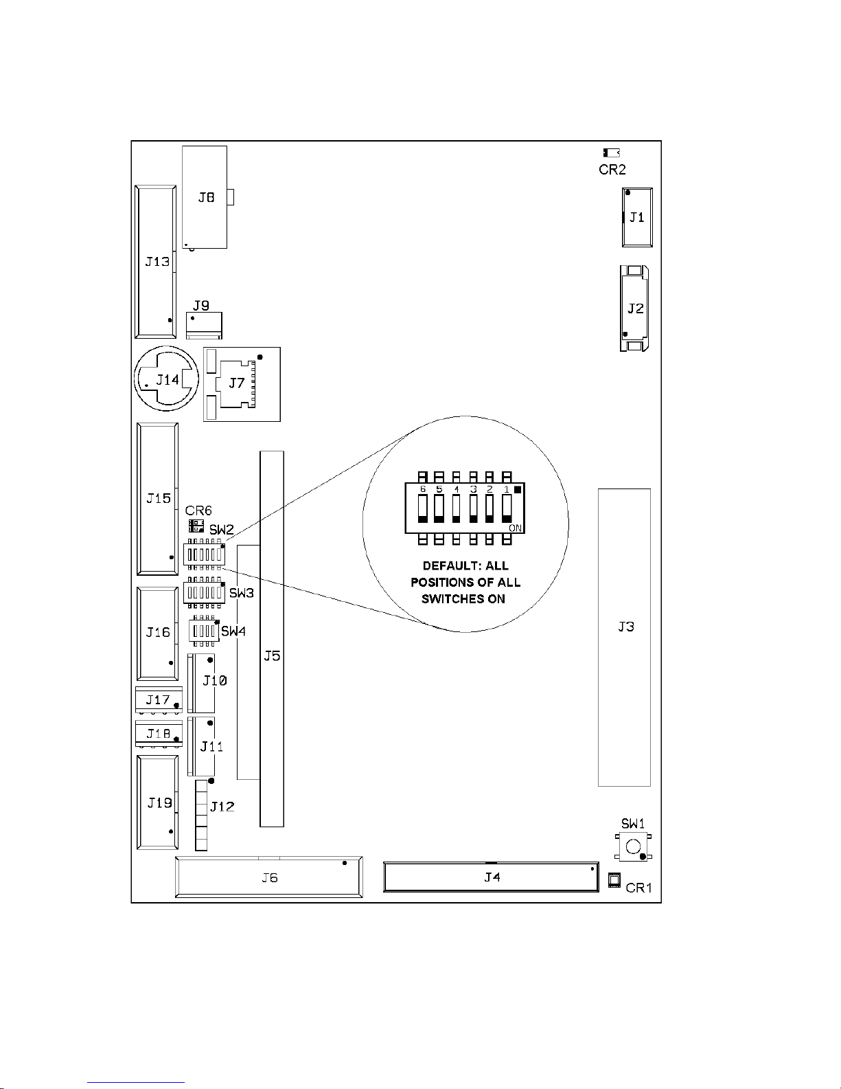
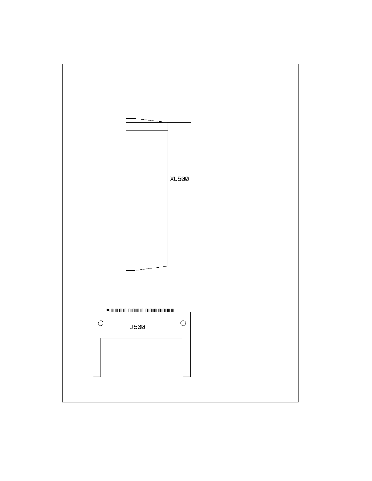
Figures 2–1 and 2–2 show the connectors and switches and their locations on the
XE–900 SBC. Figure 2–3 shows the dimensions of the XE–900 SBC in inches and
millimeters (without the Integrated Conductive Cooling System). For dimensions
and mounting diagrams with the Integrated Conductive Cooling System see page
91. The sections immediately following those figures describe the connectors and
switches, and some cables that you might require.
The XE–900 SBC contains static-sensitive CMOS components. To
avoid damaging your card and its components:
WARNING!
Ground yourself before handling the card
Disconnect power before removing or inserting a PC/104 or PC/104-
Plus expansion board.
Page 19
19
Figure 2–1 XE–900 SBC component diagram (top)
Page 20
20
Figure 2–2 XE–900 SBC component diagram (bottom)
Page 21
21
Figure 2–3 XE–900 SBC dimensions (without Integrated Conductive Cooling System)
Page 22

22
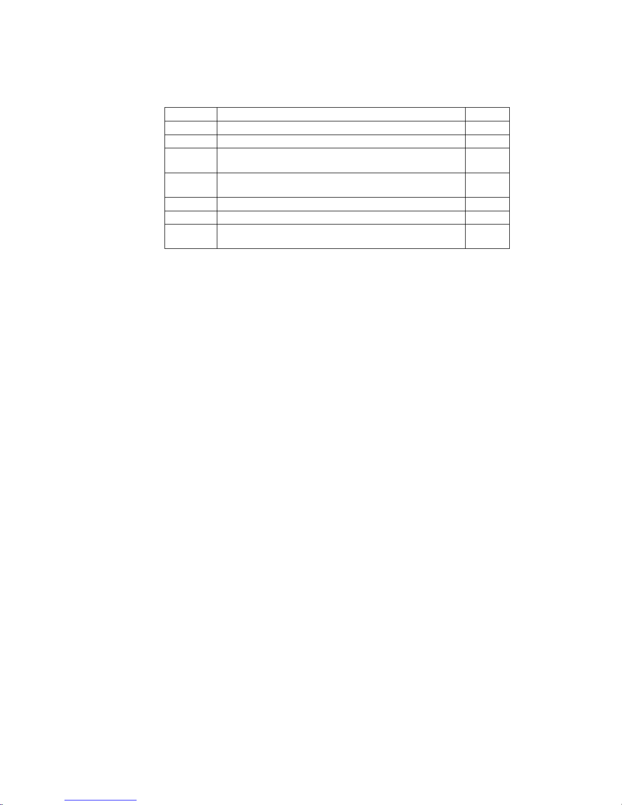
XE–900 SBC connectors and jumpers
Connector
Function
J1
VGA video
J2
LVDS video
J3
PC/104-Plus
J4
Hard drive
J5
PC/104
J6
Digital I/O
J7
Ethernet
J8
Power
J9
CPU fan
J10
COM6 RS–422/485
J11
COM5 RS–422/485
J12
COM5/6 TTL
J13
COM1/2
J14
PS/2 Keyboard / Mouse
J15
COM3/4
J16
COM5 RS–232
J17
PC battery
J18
Speaker
J19
USB1/2
J500
CompactFlash
XU500
SO-DIMM
Switch
Function
SW1
Reset
SW2
System selections
SW3
LVDS flat panel resolution
SW4
COM5/6 termination
Table 2–1 lists the connector reference designators and function for each of the
connectors. Table 2–2 lists the DIP switch reference designators and functions for
each of the switches. To view the physical location of each connector and switch
block refer to the illustration on page 19. For information on mating connectors see
page 103. For information on custom cables see the following section.
Table 2–1 XE–900 SBC connector functions
Table 2–2 XE–900 SBC switch functions
Page 23

23
Custom cables
To conserve board real estate a few connectors on the XE–900 are non-standard or
provide alternate interfaces. The cables listed below connect to the XE–900 SBC
and provide industry-standard interfaces. For ordering information see page 120.
COM PORT VTC-20F Cable. This cable connects to the 20-pin COM1/2 or
COM3/4 ports and provides two DB-9 female connectors. A VTC-20M provides
two DB-9 male connectors.
COM PORT VTC-9F Cable. This cable connects to the 10-pin COM5 port and
provides a DB-9 female connector. A VTC-9M provides a DB-9 male connector.
0.100-inch RS-422/485 Cable. This cable connects to the 5-pin header for RS-
422/485 on COM5 or COM6 and provides a standard DB-9 interface.
CMA-26 Ribbon Cable. Connects the 26-pin digital I/O port to an STB-26
Termination Board to provide access for field wiring
2 mm VGA-12 Cable. Provides a standard 15-pin VGA interface.
LVDS-18 Video Cable. Connects to the LVDS connector and provides 18-inch
flying leads
44-pin to 40-pin IDE Cable. Converts the 44-pin IDE header to a 40-pin IDE
header.
Keyboard/Mouse “Y” Cable. Connects to the PS/2 keyboard/mouse port to
provide keyboard and mouse interfaces. A keyboard will plug directly into the
XE–900 port. Available at most computer supply stores.
ATX Power Cable. Connects to the 10-pin ATX power connector and provides
a standard 20-pin ATX connector.
Two-port USB Cable. Converts the 10-pin header for USB1,2 into two
standard USB connectors.
Caution
USB devices are hot-swappable when a device is plugged into a
standard USB connector, as pins on the connectors determine the
order in which they make contact. Devices are not hot-swappable
when connected to a non-standard header. You can hot swap a
device through the USB connector on the two port USB cable, or
through another USB connector wired to the 10-pin header, but you
cannot hot swap at the 10-pin header itself.
Page 24

24
Mounting the XE–900
WARNING!
The XE–900 contains static-sensitive CMOS components. To avoid
damaging your card and its components:
Ground yourself before handling the card and observe proper ESD
precautions
Disconnect power before removing or inserting a PC/104 or PC/104-
Plus expansion board
Equipment required
To install the XE–900 SBC you will need the following equipment (or equivalent):
XE–900 SBC
+5V power supply – see the XE–900 SBC power supply requirements section.
You might also need an ATX power cable, part #6537.
A device with an operating system. The device could be a CompactFlash, hard
disk, or CD ROM. The operating system can be Windows NT, Windows CE.net,
Linux, QNX, or DOS.
PS/2 style keyboard
VGA monitor
2 mm VGA-12 Cable, part #6392
VTC-20F Cable, part #4866 (for serial console)
Null modem adapter, #2740 (for serial console)
Windows HyperTerminal or equivalent terminal emulation software (for serial
console)
Your PC (for serial console)
Hardware components required to mount the XE–900 SBC (included):
9 threaded hex standoffs (4–40 x 3/4”)
9 screws (4–40 x 3/16”)
9 internal star lock washers (#4)
9 nuts (4–40)
Refer to the XE–900 SBC component diagram, figure 2–1 on page 19, for the
location of various connectors, and to the mounting hole diagram, figure 2–3 on
page 21, for mounting the XE–900 SBC system.
With the Integrated Conductive Cooling System use 4 #10-32 screws (not included).
See page 91.
Page 25
25
Hardware mounting
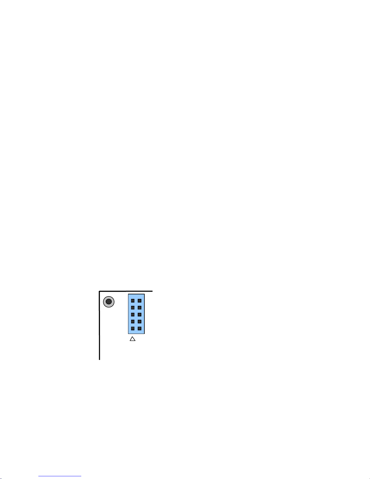
J8
1 5 6
10
1. Use the standoffs, washers, and screws and place them in the nine holes on the
XE–900 SBC board. Refer to Figure 2–3 for the center-to-center mounting hole
dimensions and for the location of the designated holes used for mounting the
hardware.
WARNING!
All nine standoffs, screws and washers must be used to secure the
XE–900 SBC. The standoffs ensure full support of the board.
WARNING!
Verify that the washers and standoffs do not touch any of the
component pads adjacent to the mounting holes. Damage will occur
at power-up.
2. Connect a 5V power source to the XE–900 SBC. Refer to the Power Supply
Requirements section, page 26. The power supply connector is located at J8.
Refer to Figure 2–4 and Table 2–3.
Note The +12V and +3V signals are routed to the PC/104 and PC/104-Plus bus only.
WARNING!
Make sure the power supply is OFF when connecting the power
cable to the XE–900 SBC board. Damage to the XE–900 SBC may
occur if the power is ON when connecting the power cable.
WARNING!
Accidentally crossing the wires, i.e., plugging +5V wires into the
ground connector or the ground wires into the +5V connector will
damage the XE–900 SBC.
Figure 2–4 Power connector, J8
Page 26

26
Table 2–3 Power connector: J8
Pin
Function
Function
Pin 1 nc
nc 6 2
GND
+5v 7 3
GND
+5v 8 4
+12V
–12V
9 5 +3V
GND
10
XE–900 SBC power supply requirements
The XE–900 SBC is designed to operate from a single +5 VDC supply, connected at
J8. If you are using the PC/104 or PC/104-Plus interface, you may also require ±12
VDC and/or +3V. The connector is a 10-pin ATX PC power supply connector, and
connects to a 10-pin ATX power supply, or with an adapter cable, to a standard 20pin ATX power supply. The typical current requirement for the XE–900 SBC is
listed in the Technical Data appendix. For the XE–900 SBC the power supply must
be able to meet the 10A inrush current.
The user should consider factors such as the power cable conductor gauge, number
and length of conductors, mating connectors, and the power requirements of
external devices such as hard drives, floppy drives, displays, mouse, and keyboard.
It is important that a quality power supply be used with the XE–900 SBC that has
sufficient current capacity, line and load regulation, hold up time, current limiting,
and minimum ripple. The power supply for the XE–900 must meet the startup
risetime requirements specified in the ATX Power Design Guide, version 1.1,
section 3.3.5. This assures that all the circuitry on the CPU control card sequences
properly and avoids system lockup.
Also, select a power supply that discharges quickly. If large power supply output
capacitors are used, powering the system down and then up may lock up the XE–
900 SBC. If the power supply does not drain below 0.7V, the CMOS components on
the XE–900 SBC will act like diodes and forward bias, potentially damaging the
XE–900 SBC circuitry.
The proper selection of a quality power supply ensures reliability and proper
functioning of the XE–900 SBC.
Page 27
27
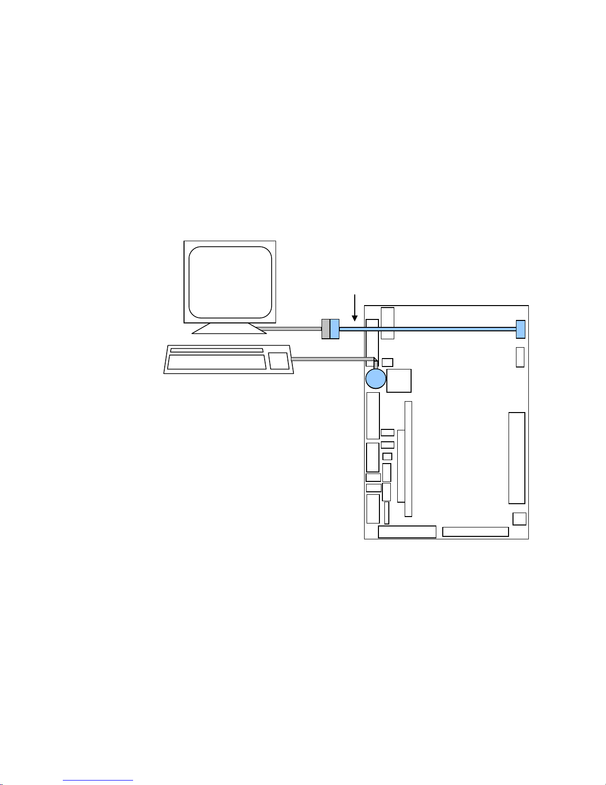
Connecting a monitor and keyboard
XE–900
PS/2 Keyboard
VGA Monitor
2 mm VGA-12 cable
.
Dot indicates pin 1
Figure 2–5 shows the XE–900 SBC with a monitor and keyboard. The following
sections describe how to connect these items.
WARNING!
The video connector on the XE–900 is keyed, but some cables are not
keyed and can be plugged in incorrectly. Ensure that pin 1 of the
cable is connected to pin 1 of the connector (indicated by the dot).
Incorrect connection could damage your equipment.
Figure 2–5 Connecting a monitor and keyboard
Monitor
The XE–900 SBC interfaces to a standard VGA monitor through the J1 connector
using a 2 mm VGA-12 cable. Connect one end of the 2 mm VGA-12 cable into J1
and connect the other end to a VGA monitor cable.
Note The video switch, SW2 position3, must be ON to use a monitor. This is the default
configuration.
Keyboard and mouse
The XE–900 SBC accepts an AT style keyboard and has a PS/2 type connector,
located at J9. The mouse port shares the keyboard connector.
Page 28

28
To use a keyboard, plug the keyboard directly into J14. To connect a mouse, use a
laptop-style “Y” connector, available at computer stores, that splits the signals into
keyboard and mouse connectors.
Note With some “Y” cables you may have to plug the mouse into the keyboard
icon, and the keyboard into the mouse icon; if the mouse and keyboard do
not function at power up, try switching them.
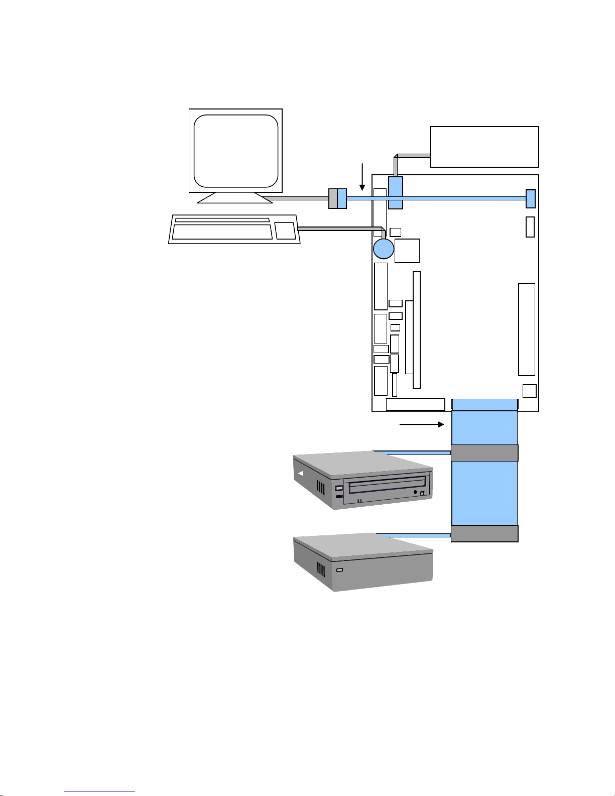
Installing an operating system
The XE–900 SBC does not come with an installed operating system. You can install
an operating system onto a hard drive or CompactFlash. Octagon Systems has OS
Embedder™ kits available for several operating systems. These kits directly
support the unique features of Octagon products, such as digital I/O, watchdog
timer, etc., eliminating the need to write special drivers. Other software kits may
also be available. Contact Octagon Systems for information concerning the software
development kits.
To install an operating system you will need:
2 mm VGA-12 video cable, #6392
PS/2 style keyboard
VGA monitor
CD-ROM drive
Operating system media
Hard drive or CompactFlash to install the operating system on to
If installing onto a hard drive, an IDE cable with master and slave connectors
OS on CD-ROM onto a hard drive or CompactFlash
Refer to Figure 2–6 on page 30 for the following:
1. Attach the 2 mm VGA-12 video cable to J1.
2. Connect the PS/2 keyboard to J14, a VGA monitor to the VGA-12 video cable,
and a CD-ROM drive to J4. Configure the CD-ROM drive as a master.
3. If using a hard drive, configure it as a slave device and install it on the IDE
cable connected to J4.
Note IDE devices have a jumper or a switch that designates whether the device is a
master or a slave device. If only one device is connected to a port, it must be
configured as a master. If two devices are connected, one must be configured as a
master and one as a slave. The XE–900 does not use the CS signal (Cable Select) to
designate master or slave on a multi-connector cable. You can use BIOS Setup to
designate either the master or the slave as a boot device.
4. If using a CompactFlash, install it into the CompactFlash socket.
Page 29

29
5. Apply power to the XE–900 SBC system. A logon message similar to the one
System BIOS Setup - Utility v5.3
(C) 2004 General Software, Inc. All rights reserved
>Information Browser
Basic CMOS Configuration
Features Configuration
Custom Configuration
PnP Configuration
Shadow Configuration
Reset CMOS to last known values
Reset CMOS to factory defaults
Write to CMOS and Exit
Exit without changing CMOS
↑/↓/←/→/CR/<Tab> to select. <Esc> to continue (no save)
www.gensw.com
below will appear on your PC monitor:
General Software P6 Class Embedded BIOS(R) 2000 Revision 5.3 Copyright (C)
2004 General Software, Inc. All rights reserved. Octagon Systems XE900
00000589K Low Memory Passed
00117632K Ext Memory Passed
Wait.....
6. Enter Setup by pressing the Del key or Ctrl-C during BIOS POST sequence
(this occurs between the memory test and bootup).
Note Your display message may be slightly different
7. Configure the CD–ROM as a master device in BIOS Setup, and change the boot
sequence to CD-ROM drive first. Designate the hard drive or CompactFlash as
drive c:.
8. Insert the operating system media into the CD-ROM drive.
9. Reboot the system. The system should boot to the CD-ROM.
10. Follow the on-screen dialog to load the operating system. Refer to the OS
documentation for further information.
Page 30
30
Figure 2–6 Installing an operating system
XE–900
PS/2 Keyboard
VGA Monitor
2 mm VGA-12 cable
.
Dot indicates pin 1
Power Supply
CompactFlash installed into
CompactFlash socket on back of board
CD-ROM
and / or
Hard Drive
IDE ribbon cable for two devices, or
one device directly into J4
Page 31

31
Chapter 3: Setup programs
This chapter discusses running the Setup configuration program on the XE–900
SBC. Setup configures devices set up by the BIOS such as serial ports, floppy
drives, etc.
Setup
Setup can be entered by pressing the “Delete” key on the system keyboard or Ctrl-C
when POST I/O has been redirected to a serial console during the BIOS POST
sequence (this occurs between the memory test and boot).
Also, by setting the “S” switch Off (Switch 2 position 1), you will force the Setup to
revert to the factory-programmed defaults shown in the following menus. This
allows you to boot with a known set of parameters. If you want to use the default
settings for future boots, you must enter Setup and “Save” for the default values to
be stored in CMOS.
Note The Setup defaults might vary slightly from those shown in the following menus
depending on the BIOS revision on your card.
The system will display the XE–900 General Software System BIOS Setup Utility
menu. Select the submenu by using the up/down arrows, then press <ENTER>
(when using a monitor connected to the XE–900 SBC). For a serial console
configuration, Ctrl + E is up and Ctrl + X is down.
Page 32

32
System BIOS Utility menu
System BIOS Setup - Utility v5.3
(C) 2004 General Software, Inc. All rights reserved
>Information Browser
Basic CMOS Configuration
Features Configuration
Custom Configuration
PnP Configuration
Shadow Configuration
Reset CMOS to last known values
Reset CMOS to factory defaults
Write to CMOS and Exit
Exit without changing CMOS
↑/↓/←/→/CR/<Tab> to select. <Esc> to continue (no save)
www.gensw.com
The Utility menu allows you to select the appropriate menus for configuration. The
menus shown below are described on the following pages. Default values are shown
in the menus.
Information Browser menu
The Information Browser provides information specific to the XE–900, as well as
contact information for Technical Support.
Page 33

33
Basic CMOS Configuration menu
System BIOS Setup - Basic CMOS Configuration
(C) 2004 General Software, Inc. All rights reserved
DRIVE ASSIGNMENT ORDER
Drive A: (None)
Drive B: (None)
Drive C: Ide 0/CF socket
Drive D: (None)
Drive E: (None)
Drive F: (None)
Drive G: (None)
Drive H: (None)
Drive I: (None)
Drive J: (None)
Drive K: (None)
Boot Method: Boot Sector
Date:
Time:
Numlock: Disabled
Typematic Delay : 250 ms
Typematic Rate : 30 cps
Seek at Boot : None
Show “Hit Del” : Enabled
Config Box : Enabled
F1 Error Wait : Enabled
Parity Checking : (Unused)
Memory Test Tick : Enabled
Debug Breakpoints : (Unused)
Debugger Hex Case : Upper
Memory Test : StdLo FastHi
BOOT ORDER
Boot 1st: Drive C:
Boot 2nd: Browser
Boot 3rd: None
Boot 4th: None
Boot 5th: None
Boot 6th: None
ATA DRV ASSIGNMENT: Sect Hds Cyls
Ide 0: 3 = AUTOCONFIG, LBA
Ide 1: Not installed
Ide 2: 3 = AUTOCONFIG, LBA
Ide 3: 3 = AUTOCONFIG, LBA
Memory
Base:
632KB
Ext:
251MB
FLOPPY DRIVE TYPES:
Floppy 0: Not installed
Floppy 1: Not installed
↑/↓/←/→/CR/<Tab> to select or <PgUp>/<PgDn>/+/- to modify
<Esc> to return to main menu
Default values are shown in the menu.
DRIVE ASSIGNMENT ORDER: These selections allow you to assign the various drives installed
to a designated alphabetic drive.
Note If using a floppy drive, assign a drive to A before assigning a drive to B (do
not assign a drive to Drive B, but not Drive A). Do not skip drive C if using
flash / hard drives (the first flash / hard drive should be drive C). If using a
CD-ROM, DO NOT assign a drive letter to its IDE port; the operating
system will automatically assign a drive letter to CD-ROMs.
Do not assign the same file system to more than one drive without
considering the consequences (such as assigning IDE0 to Drive C and Drive
D). This is allowed to enable aliasing of drives; however this may cause
corruption of operating system cache and state unless the OS is configured
for this as well. Many desktop operating systems cannot be so configured.
Drive A/B: Selections are None, Floppy 0, Floppy 1. See note above.
Drive C/D: Selections are None, Floppy 0, Floppy 1, Ide 0/CF socket, Ide 2/Ext Master,
Ide 3/Ext Slave. See note above, particularly if using a CD-ROM.
Drive E/F/G/H/I/J/K: Selections are None, Ide 0/CF socket, Ide 2/Ext Master, Ide 3/Ext Slave. See
note above, particularly if using a CD-ROM.
Boot Method: Selections are Windows CE or Boot Sector. For normal boot, select Boot
Sector. Windows CE users may be able to load their Windows CE
environment without a DOS or other bootable environment by selecting the
Windows CE option. This will cause the BIOS to attempt to find the
FLOPPY DRIVE TYPES: These selections allow you to specify the type of floppy device for
Windows CE system file (NK.BIN) on boot disks.
Floppy 0 and Floppy 1. The XE–900 supports USB floppies and PC/104 or
PC/104-Plus floppies. The selections are 360 KB, 5.25”; 1.2 MB, 5.25”; 720
Page 34

34
KB, 3.5”; 1.44 MB, 3.5”; 2.88 MB, 3.5”; Not installed. Note that the XE–900
does not support a floppy drive directly. This feature should be left Not
Installed if you are not using a floppy drive; for USB floppies this should
also be left as Not Installed. This frees up INT6 for other applications.
System Date: Sets the date for the system clock.
System Time: Sets the time for the system clock.
NumLock: Enables or disables NumLock.
BOOT ORDER: These selections specify the order of the devices or events which will be
used to boot the XE–900. The selections are Drive A, Drive B, Drive C,
Drive D, Reboot, CDROM, or None.
Note The first None stops the boot sequence; any subsequent settings in boot
order after None will have no effect. The Reboot option will cause the
system to attempt to reboot if the previous boot selections fail. This option
requires System Management Mode to be enabled (see Features
Configuration screen.)
ATA DRIVE ASSIGNMENT: These selections allow you to specify the type of devices for IDE 0,
1, 2, and 3. IDE 0 is hardwired to the CompactFlash socket; Ide1 is
unavailable. Note that the XE–900 SBC only supports three IDE devices
total (CompactFlash and two Secondary devices.) The available options are
Not Installed; User Type; AUTOCONFIG, PHYSICAL; AUTOCONFIG,
LBA; AUTOCONFIG, PHOENIX, and IDE CDROM. User Type allows you
to set parameters for Sectors (63 max.), Heads (255 max.) and Cylinders
(1023 max.).
Note The AUTOCONFIG, PHYSICAL; AUTOCONFIG, LBA; and
AUTOCONFIG, PHOENIX options refer to the BIOS of the system which
was used to format the hard drive or CompactFlash. If you have formatted
a hard drive or a CompactFlash on another system than the XE–900, you
might have to change this setting for the XE–900 to recognize the drive.
Typematic Delay: Sets the time before a character will repeat when a key is continuously
depressed. Selections are Disabled, 250 ms, 500 ms, 750 ms, and 1000 ms.
Typematic Rate: Sets the rate at which a character will repeat when a key is continuously
depressed. Selections are 30 cps, 24 cps, 20 cps, 15 cps, 12 cps, 10 cps, 8 cps,
and 6 cps.
Seek at Boot: Selections are None, Floppy, Ide, Both. For faster boot, the default setting
(None) does not perform floppy or IDE seek operations during POST. In
rare cases, some drives may not properly initialize without this seek
operation. For this reason, users may select to seek Floppy drives, IDE
drives, or both during POST if desired.
Show “Hit Del”: Enabled or Disabled. When enabled, the “Hit Del to access Setup” message
is displayed during boot.
Config Box: Enabled or Disabled. When enabled, the blue Configuration box will appear
on screen during boot.
F1 Error Wait: Enabled or Disabled. When enabled, the system will pause at a boot error
until the F1 key is pressed.
Parity Checking: This function is not used.
Memory Test Tick: Enabled or Disabled. When enabled the system produces an audible tick
during the memory test at boot.
Page 35

35
Debug Breakpoints: This function is not used.
System BIOS Setup - Feature Configuration
(C) 2004 General Software, Inc. All rights reserved
ACPI 2.0 :>Enabled
Graphical/Audio POST : Enabled
System Management Bus : Disabled
Primary IDE UDMA : Disabled
System Management Mode : Enabled
System Management BIOS : Enabled
Console Redirection : Auto
Secondary IDE UDMA : Disabled
↑/↓/←/→/CR/<Tab> to select or <PgUp>/<PgDn>/+/- to modify
<Esc> to return to main menu
Debugger Hex Case: Upper or Lower. Selects the case for debugger output.
Memory Test: This item allows you set the test speed for both the base memory (Lo) and
the extended memory (Hi). The options are Fast, Standard, or Full.
System Memory: Displays the amount of system memory on the card.
Extended Memory: Displays the amount of extended memory on the card.
Features Configuration menu
The Features Configuration menu allows you to set some of the system features.
Default values are shown in the menu.
ACPI 2.0: Enabled, disabled. When enabled, the BIOS supports the Advanced
Control Program Interface, level 2.0. ACPI combines the resource
assignment capabilities of PnP and the power management
functionality similar to APM.
Graphical/Audio POST: Enabled, disabled. When enabled, the graphical splash screen is
shown during POST, along with a short sound played through the
PC Speaker. If disabled, the text POST screen is displayed. This
feature is not available with a serial console.
System Management Bus: Enabled, disabled. When enabled, the BIOS supports the SMBus
BIOS interface to allow the operating system to interact with
devices on the System Management Bus.
Primary IDE UDMA: Enabled, disabled. When enabled, UDMA is available on the
primary IDE interface. Note: CompactFlash devices do not support
UDMA.
System Management Mode: Enabled, disabled. When enabled, the BIOS’s System Management
Mode environment is enabled. This allows use of Legacy USB
devices, including keyboards or mice without OS drivers.
System Management BIOS: Enabled, disabled. When enabled, the BIOS supports the industry
standard System Management BIOS (formerly known as the
Desktop Management Interface, or DMI).
Console Redirection: Auto, redirect. When set to Auto, the console will be redirected to
the serial port COM1 in the event that no video controller is found
(V switch is OFF) or if a carriage return is received on COM1
during POST. When set to Redirect the console is forced to redirect
to COM1 even if a video console is available.
Secondary IDE UDMA: Enabled, disabled. When enabled , UDMA is available on the
Page 36

36
secondary IDE interface.
System BIOS Setup - Custom Configuration
(C) 2004 General Software, Inc. All rights reserved
COM3-6 Enable (See doc.) :>Normal
COM5 Mode : RS232/422
COM6 Mode : RS232/422
Digital I/I Base Address : 0x120
Watchdog Timer : Disabled
RAM Reserved for Video : 8 MB
AGP Aperture Size : 128
CRT Analog Output : Enabled
DMA Channel to Disable : DMA2
↑/↓/←/→/CR/<Tab> to select or <PgUp>/<PgDn>/+/- to modify
<Esc> to return to main menu
Port
Normal Base Address
Alternate Base Address
COM3
0x3E8
0x3E8
COM4
0x2E8
0x2E8
COM5
0x1A8
0x1C8
COM6
0x1A0
0x1C0
Note UltraDMA modes are not supported directly by the XE–900. These modes require
an 80-pin connector, and there is no adapter available for the 44-pin, 2mm IDE
connector used on the XE–900.
Custom Configuration menu
The Custom Configuration menu allows you to set parameters for COM3-6, digital
I/O, watchdog timer, video, and DMA channel reserved for system use. Default
values are shown in the menu.
COM3-6 Enable: Normal, Disabled, Alternate. This item enables or disables COM3-6
Note: COM1 is always enabled at base address 0x3F8, using IRQ 4;
COM5 Mode: RS232/422, RS485. This item selects two-wire RS485, or four-wire
COM6 Mode: RS232/422, RS485. This item selects two-wire RS485, or four-wire
Digital I/O base Address: 0x120h, 0x320h, or disabled. Sets the base address for digital I/O.
Watchdog: Enabled, Disabled. Enables watchdog timer.
RAM reserved for Video: Disabled, 8MB, 16MB, 32MB. Specifies the amount of RAM
API Aperture Size: 2, 4, 8, 16, 32, 64, or 128. Sets the size for the API aperture.
for serial operation. COM3 through COM6 share IRQ9. The
Disabled option disables I/O to COM3 through COM6. Normal and
Alternate select the base address of COM3 through COM6 as shown
below; only COM5 and COM6 are changed.
COM2 is always enabled at base address 0x2F8, using IRQ 3. IRQ9
is always used by COM3-6 even if disabled. IRQ9 is NOT available
for PC/104 devices.
operation (RS232/422 or TTL) for COM5.
operation (RS232/422 or TTL) for COM6.
reserved for video.
Page 37

37
CRT Analog Output: Enabled, disabled. When using a flat panel this must be disabled.
System BIOS Setup - Plug-n-Play Configuration
(C) 2004 General Software, Inc. All rights reserved
Enable PnP Support :>Enabled
Assign IRQ0 to PnP :Disabled
Assign IRQ1 to PnP :Disabled
Assign IRQ2 to PnP :Disabled
Assign IRQ3 to PnP :Enabled
Assign IRQ4 to PnP :Enabled
Assign IRQ5 to PnP :Disabled
Assign IRQ6 to PnP :Enabled
Assign IRQ7 to PnP :Enabled
Assign DMA0 to PnP :Disabled
Assign DMA1 to PnP :Disabled
Assign DMA2 to PnP :Disabled
Assign DMA3 to PnP :Enabled
Enabled PnP O/S :Enabled
Assign IRQ8 to PnP :Disabled
Assign IRQ9 to PnP :Enabled
Assign IRQ10 to PnP :Enabled
Assign IRQ11 to PnP :Enabled
Assign IRQ12 to PnP :Disabled
Assign IRQ13 to PnP :Enabled
Assign IRQ14 to PnP :Disabled
Assign IRQ15 to PnP :Disabled
Assign DMA4 to PnP :Enabled
Assign DMA5 to PnP :Enabled
Assign DMA6 to PnP :Enabled
Assign DMA7 to PnP :Enabled
↑/↓/←/→/CR/<Tab> to select or <PgUp>/<PgDn>/+/- to modify
<Esc> to return to main menu
System BIOS Setup - Shadow/Cache Configuration
(C) 2004 General Software, Inc. All rights reserved
Shadowing :>Chipset
Shadow 16KB ROM at C400 :Enabled
Shadow 16KB ROM at CC00 :Disabled
Shadow 16KB ROM at D400 :Disabled
Shadow 16KB ROM at DC00 :Disabled
Shadow 16KB ROM at E400 :Enabled
Shadow 16KB ROM at EC00 :Enabled
Shadow 16KB ROM at C000 :Enabled
Shadow 16KB ROM at C800 :Disabled
Shadow 16KB ROM at D000 :Disabled
Shadow 16KB ROM at D800 :Disabled
Shadow 16KB ROM at E000 :Enabled
Shadow 16KB ROM at E800 :Enabled
Shadow 16KB ROM at F000 :Enabled
↑/↓/←/→/CR/<Tab> to select or <PgUp>/<PgDn>/+/- to modify
<Esc> to return to main menu
DMA Channel to Disable: DMA0, 1, 2, 3. The system requires one DMA channel for internal
use. Whichever channel is selected will not be available on the ISA
bus.
Plug-n-Play Configuration menu
The Plug-n-Play Configuration menu allows you to select IRQs and DMA channels
for use by plug-n-play devices. Default values are shown in the menu.
Shadow/Cache Configuration menu
The Shadow/Cache Configuration menu enables shadowing and selects the address
where it will be stored. Shadowing is disabled by selecting None under Shadowing.
Default values are shown in the menu.
Page 38

38
Page 39

39
Writing to CMOS and exiting
The last four items in the Utility menu give you a Yes or No option when you select
them. Selecting Yes will implement the item. Selecting No will return you to the
Utility menu. Those four selections are:
Reset CMOS to last known values
This item restores the values that were in CMOS at boot, without exiting
Setup.
Reset CMOS to factory defaults
Write to CMOS and Exit
Exit without changing CMOS
Page 40

40
Overview: Section 2 – Hardware
Section 2 discusses usage, functions, and system configurations of the
XE–900 SBC major hardware features. The following chapters are included:
Chapter 4: Serial ports
Chapter 5: Console devices
Chapter 6: CompactFlash, SDRAM, and battery backup
Chapter 7: External drives
Chapter 8: Bit-programmable digital I/O
Chapter 9: CRTs and LVDS flat panels
Chapter 10: Ethernet
Chapter 11: PC/104 and PC/104-Plus expansion
Chapter 12: USB
Page 41

41
Chapter 4: Serial ports
Description
The XE–900 SBC has six serial ports, COM1 through COM6. COM1 is a dedicated
8-wire RS–232C. COM2, COM3, and COM4 are dedicated 4-wire RS–232C. COM5
can be 4-wire RS–232C, RS–422, RS–485, or TTL. COM6 can be 4-wire RS–422,
RS–485, or TTL.
COM1 and COM2 are accessed at the 20-pin connector at J13. COM3 and COM4
are accessed at the 20-pin connector at J15. COM5 and COM6 have separate
connectors for the supported interfaces. Refer to the table on page 22 for which
connector to use for the various interfaces. Refer to the Custom Cables section on
page 23 for a description of cables that mate with these connectors.
These serial ports interface to serial device. All ports support 5-, 6-, 7-, or 8-bit
word lengths, 1, 1.5, or 2 stop bits, and baud rates up to 115.2K.
The serial ports have the following specifications:
16C550 compatible
16-byte FIFO buffers
IEC 1000, level 3, ESD protection
— Contact discharge ±6 kV
— Air–gap discharge ±8 kV
Backdrive protection
Up to 115.2k baud operation
Mating receptacles
Use a VTC–20F or VTC–20M cable to connect the 20-pin COM ports to external
serial equipment. The P2 and P3 connectors on these cables are DB–9 female
(VTC–20F) or DB–9 male (VTC–20M) connectors which plug directly into a 9-pin
serial cable. Use a VTC–9F or VTC–9M to connect the 10-pin COM5 RS–232C port
to external serial equipment For RS-422 or RS-485 on COM5 or COM6, use a 0.100
inch RS422/485 Cable (part #6683).
Figure 4–1 (following page) shows serial devices connected to the XE–900 SBC. It
also shows the schematic for connecting RS–422, RS–485 and TTL devices. Note
that you cannot use COM5 or COM6 for two different interfaces at the same time.
Figure 4–2 shows a null modem adapter connected to the COM1 port of a VTC–
20F. A null modem adapter is required when connecting a serial console.
Serial port configurations
COM1 and COM2 are always enabled. COM3-6 can be configured in Setup in the
Custom Configuration menu. The selections are Normal, Alternate, and Disabled.
Normal and Alternate select different addresses for COM5 and COM6. See Table
4–1 on page 43. You must also select the Mode for COM5 and COM6. For RS–232C,
RS–422 or TTL select RS232/422. For RS–485 select RS485. For additional
Page 42

42
information on Setup menus see page 36.
VTC-20F Cable
P3
P2
Null Modem Adapter,
required for serial console
COM2
COM1
Serial Device
on COM2
Serial Device
on COM1
RS–422 or RS–485
Device on COM6
0.100-inch RS–422/485 cable
VTC-20F cable
XE–900
TTL Device on COM5
Up to six serial devices total; four or five
RS–232, one or two RS–422, RS–485, or TTL.
COM3/4 RS–232
COM5 RS–232
COM5 RS–422/485
COM5/6 TTL
If COM5 or COM6 are used for RS–422 or RS–485, and the XE–900 is at the end of
the network, these ports will have to be terminated. Switch 4 terminates the
network. The default setting is terminated. If the XE–900 is not at the end of the
network the switch must be set to unterminated.
COM3 through COM6 all share interrupt 9. Even when these ports are disabled
interrupt 9 is not available for PC/104 devices.
The COM ports configurations are shown in table 4–1. Tables 4–2 through 4–6
show the COM pin-outs for the COM ports, and table 4–7 shows the switch
settings.
Figure 4–1 COM ports
Figure 4–2 VTC-20F cable and null modem adapter
Page 43

43
Table 4–1 Serial port configurations
COM Port
Address
IRQ
Interface
BIOS
Setup
Connector
COM1
3F8h
IRQ4
RS–232 – 8 wire
NA
J13
COM2
2F8h
IRQ3
RS–232 – 4 wire
NA
J13
COM3
3E8h
IRQ9
RS–232 – 4 wire
Normal
J15
COM4
2E8h
IRQ9
RS–232 – 4 wire
Normal
J15
COM5
1A8*
1C8
IRQ9
RS–232 – 4 wire
(COM5 Mode RS232)
Normal*
Alternate
J16
COM5
1A8*
1C8
IRQ9
RS–422 – 4 wire
(COM5 Mode RS232)
Normal*
Alternate
J11
COM5
1A8*
1C8
IRQ9
RS–485 – 2 wire
(COM5 Mode RS485)
Normal*
Alternate
J11
COM5
1A8*
1C8
IRQ9
TTL
(COM5 Mode RS232)
Normal*
Alternate
J12
COM6
1A0*
1C0
IRQ9
RS–422 – 4 wire
(COM6 Mode RS232)
Normal*
Alternate
J10
COM6
1A0*
1C0
IRQ9
RS–485 – 2 wire
(COM6 Mode RS485)
Normal*
Alternate
J10
COM6
1A0*
1C0
IRQ9
TTL
(COM6 Mode RS232)
Normal*
Alternate
J12
* This address is used when Normal is selected in Setup. The other address is used
when Alternate is selected.
COM1
COM2
DB–9 Pinout
Pin#
RS–232
signal
Pin#
RS–232
signal
DB–9
pin#
DB–9
pin#
1
2
3
4
5
6
7
8
9
10
DCD
DSR
RxD
RTS
TxD
CTS
DTR
RI
GND
nc
11
12
13
14
15
16
17
18
19
20
nc
nc
RxD
RTS
TxD
CTS
nc
nc
GND
nc
1
2
3
4
5
6
7
8
9
Table 4–2 COM1 and COM2 connector pin-outs (J13 connector)
Page 44

44
Table 4–3 COM3 and COM4 connector pin-outs (J15 connector)
COM3
COM4
DB–9 Pinout
Pin#
RS–232
signal
Pin#
RS–232
signal
DB–9
pin#
DB–9
pin#
1
2
3
4
5
6
7
8
9
10
nc
nc
RxD
RTS
TxD
CTS
nc
nc
GND
nc
11
12
13
14
15
16
17
18
19
20
nc
nc
RxD
RTS
TxD
CTS
nc
nc
GND
nc
1
2
3
4
5
6
7
8
9
COM5 RS–232
DB–9 Pinout
Pin#
RS–232
signal
DB–9
pin#
DB–9
pin#
1
2
3
4
5
6
7
8
9
10
nc
nc
RxD
RTS
TxD
CTS
nc
nc
GND
nc
1
2
3
4
5
6
7
8
9
J11 COM5
connector
J10 COM6
connector
DB–9 connector
Pin #
Signal
Pin #
Signal
Pin #
Pin #
1
TXD+
1
TXD+
1 2
TXD–
2
TXD–
6
nc nc 2 nc nc 7 nc nc 3 nc nc 8 4 RXD+
4
RXD+
4 5
RXD–
5
RXD–
9 3*
GND
3
GND
5 *Note that pin 3 is not listed in numerical order.
Table 4–4 COM5 RS–232 connector pin-out (J16 connector)
Table 4–5 COM5 and COM6 RS–422/485 connector pin-outs and pin-out for 0.100-inch
RS–422/485 cable
Page 45

45
Table 4–6 COM5 and COM6 TTL connector pin-out (J12 connector)
J12 COM5/6
TTL connector
Pin #
Signal
1
TX5 2 RX5
3
GND
4
TX6 5 RX6
6
GND
Switch 4 – COM5/6 termination
COM Port
Interface
Switch 4 Settings
COM5
RS–422/RS–485
no termination
Position 1 Off
Position 2 Off
RS–422/RS–485
with termination
Position 1 On*
Position 2 On*
COM6
RS–422/RS–485
no termination
Position 3 Off
Position 4 Off
RS–422/RS–485
with termination
Position 3 On*
Position 4 On*
* Default. These switches terminate the network. If
the XE–900 SBC is not at an end of the network, set
these switches to Off .
Table 4–7 COM5/6 switches, Switch 4
Function and use of serial ports
COM1 as serial console device
You can use COM1 as a console device to communicate with another PC. For COM1
to be a serial console, the “V” video switch (Switch 2 position 3) must be set to Off.
You can also redirect the video output to a serial console on COM1 by hitting the
carriage return (Enter) on the host keyboard during boot. See the Console devices
chapter for more information.
Note When interfacing the XE–900 SBC to your desktop PC, you must use a null modem
adapter.
COM2 through COM5 as RS–232 I/O
COM1 is an 8-wire RS–232 interface. COM2 through COM4 are dedicated 4-wire
RS–232 interfaces. COM5 can also be configured through Setup as a 4-wire RS–232
interface. You can connect up to five RS–232 serial I/O devices.
COM5/6 as TTL interface
COM5 and COM6 can be used as a TTL interface. The configuration for COM5 and
Page 46

46
COM6 is selected in Setup under COM5 Mode and COM6 Mode. For TTL, select
Receiver
Xmitter
100
100
TX –
RX +
TX +
RX –
Gnd
100
Receiver
Xmitter
100
RX –
TX +
TX –
RX +
RS232/422.
One use of a TTL interface is for a TTL-level GPS module. AN RTCM SC-104
differential GPS module uses both COM ports. Some GPS modules only require one
port, in which case the other port could be configured for other serial interfaces.
COM5/6 as RS–422 and RS–485 networks
COM5 and COM6 can also be used as RS–422 or RS–485. RS–422 and RS–485 use
differential signaling to communicate between the devices on a network.
Differential signal reduces the effect of environmental noise, allowing
communication over distances up to 1200 meters.
The RS–422 and RS–485 receivers provide an active high (space) condition for
shorted, open, or inactive lines. Note that RTS is used differently by RS–422 and
RS–485. Review the information in the following sections regarding RTS.
RS–422 is a point-to-point configuration. RS–485 is a multi-node configuration that
allows up to 32 nodes on a network. COM5 and COM6 can be configured in BIOS
Setup for RS–422 or RS–485. Refer to table 4–7 on page 45 for switch settings for
terminating an RS–422/485 network.
RS–422
RS–422 is typically point to point configuration. RS–422 is also specified for multidrop (party-line) applications where only one driver is connected to, and transmits
on, a “bus” of up to 10 receivers. The device at the end of an RS–422 network must
be terminated. The XE–900 SBC optionally terminates with a 100 ohm resistor.
Refer to table 4–7. Figure 4–3 shows a typical RS–422 four-wire interface circuit.
The RTS* signal is used to control the transmitter and receiver in RS–422 mode.
The RTS* signal is controlled by the Modem Control Register bit 1 (MCR[1], which
is offset 0x04 from the UART base address). Writing MCR[1] to 0 (default state)
sets RTS* to an inactive state (RTS* = logic high) which ENABLES both the RS–
422 Transmitter and Receiver. Writing MCR[1] to 1 sets RTS* to an active state
(RTS* = logic low) which DISABLES both the RS–422 Transmitter and Receiver.
Figure 4–3 Typical RS–422 four-wire interface circuit
RS–485
An application may implement a node as either the “host” node or as a “remote”
Page 47

47
node in an RS–485 network. There can be as many as 32 nodes without any bus
RO
RE
Xmitter
TX +
TX –
Receiver
100
100
Receive
Receiver
Receiver
Xmitter
Xmitter
TX +
120
RE
RE
repeaters in the network. A host is referred to as the node that initiates
communication; a remote is referred to as a node that is addressed by the host.
In any given communication sequence in an RS–485 network, there can only be one
host. The host is responsible for initiating communication, maintaining network
registration, and providing housekeeping tasks with other nodes. Remotes,
however, cannot initiate a communication. They can only respond to messages that
are addressed to them from the host.
The devices at each end of an RS–485 network must be terminated. Any node
located between the end points should not be terminated. The XE–900 SBC
optionally terminates with a 100 ohm resistor. Refer to table 4–7 on page 45.
Figure 4–4 shows a typical RS–485 network. Note that for 2-wire RS–485 networks
the transmit and receive pairs must be connected together external to the XE–900
(TXD+ tied to RXD+, TXD– tied to RXD–).
The RTS* signal is used to control the transmitter and receiver in RS–485 mode.
The RTS* signal is controlled by the Modem Control Register bit 1 (MCR[1], which
is offset 0x04 from the UART base address). Writing MCR[1] to 0 (default state)
sets RTS* to an inactive state (RTS* = logic high) and DISABLES the RS–485
Transmitter and ENABLES the Receiver. Writing MCR[1] to 1 sets RTS* to an
active state (RTS* = logic low), and ENABLES the RS–485 Transmitter and
DISABLES the RS–485 Receiver.
Figure 4–4 Typical RS–485 two–wire half duplex interface circuit
Page 48

48
Chapter 5: Console devices
Description
The XE–900 SBC has three options for console devices. You can use a monitor and
a keyboard as your console. You can use COM1 as the console, or you can run the
system without a console device.
Selecting console devices
The following represent the options on the XE–900 SBC for console devices:
A standard VGA/SVGA monitor and a keyboard.
Serial console from COM1. A serial cable/null modem adapter plugged into a
host PC running HyperTerminal (or equivalent) provides both input and
output. The local keyboard also allows input but is not required.
No console device means no video output, either from a monitor or the serial
console. A local keyboard allows input but is not required.
Monitor and keyboard console
To use a monitor and keyboard as the console, you will need the following
equipment (or equivalent):
XE–900 SBC
2 mm VGA-12 video cable, #6392
PS/2 style keyboard
VGA monitor
WARNING!
The video connector is keyed, but some connectors are not keyed
and can be plugged in incorrectly. Ensure that pin 1 of the cable is
connected to pin 1 of the connector (indicated by the dot). Incorrect
connection could damage your equipment.
To connect a monitor and keyboard:
1. Refer to Figure 2–1 on page 19 for the location of various connectors and
switches before installing the XE–900 SBC.
2. Make sure that the “V” video switch, Switch 2 position 3, is set to On.
3. Connect the VGA-12 video cable into J1.
4. Connect a VGA monitor to the VGA-12 cable, and a PS/2 style keyboard to J14.
5. If you want a mouse, use a “Y” style PS/2 adapter in J14. This allows both a
mouse and a keyboard to be connected. Note that with some “Y” cables you may
Page 49

49
have to plug the mouse into the keyboard icon, and the keyboard into the
XE–900
PS/2 Keyboard
VGA Monitor
2 mm VGA-12 cable
.
Dot indicates pin 1
Power Supply
mouse icon; if the mouse and keyboard do not function at power up, try
switching them.
Figure 5–1 Monitor and keyboard as console
Serial console
COM1 is used as the console device if the Console Redirection in the Features
Configuration menu is set to Redirect. COM1 will also be configured as a console
device if a host computer is connected to COM1 and the host keyboard sends a
carriage return (Enter) during the boot process.
Note that you cannot use a serial console for a GUI interface due to the large
volume of data. It can only be used with a text-based OS such as DOS.
To use COM1 as the console, you will need the following equipment (or equivalent):
XE–900 SBC
VTC-20F cable, #4866
Null modem adapter, #2470 (9–pin to 9–pin)
Host computer running HyperTerminal (or equivalent)
Serial cable to connect XE–900 SBC COM1 to host computer serial port
PS/2 style keyboard (optional)
Page 50

50
Connect using:
Direct to COM1, COM2, COM3, or COM4
(select the port the serial cable is connected to)
Baud rate:
115200
Communications
parameters:
no parity, 8 data bits, 1 stop bit
Flow control:
none
Terminal support:
ANSI
ANSI terminal option–
Wrap lines that exceed
terminal width:
Yes (uncheck box)
Refer to Figure 2–1 on page 19 for the location of various connectors and switches
before installing the XE–900 SBC.
1. Set the “V” video switch, Switch 2 position 3, to Off. An alternative way to
redirect the video to a serial console is to hit the carriage return (Enter) key on
the host keyboard. This will redirect the video regardless of switch settings or
BIOS settings.
2. Connect a VTC-20F cable to J13 of the XE–900.
3. Connect the null modem adapter to P2 (COM1 side) of the VTC-20F cable.
4. Connect the serial cable between the null modem adapter and the serial port of
the host computer.
Follow these steps to use the serial console:
5. For communication using HyperTerminal (or equivalent), the following settings
must be used:
6. Start HyperTerminal. You are now ready to establish communications between
the host PC and the XE–900 SBC.
7. Power on the XE–900 SBC. Console data will be redirected to COM1 and will
be displayed on the host computer.
8. If you do not get the proper logon message check the HyperTerminal serial
parameters of the host PC to make sure they match the settings in step 5. You
might also try setting the “S” switch, Switch 2 position1, to Off to force the XE–
900 SBC card to the system defaults, which includes 115200 baud rate.
Note Function keys entered on the host computer do not transmit across a serial console.
Hot key access to serial console
In some instances you might want to redirect the video to a serial console without
having reconfigured Setup or setting the V switch to Off. If you have connected a
serial console to COM1, pressing the Enter key on the host keyboard during the
boot process will redirect video to the serial console.
Page 51

51
Figure 5–2 The XE–900 SBC and a serial console
XE–900
COM2
COM1
VTC-20F cable
Keyboard
HyperTerm
or other
terminal emulator
Desktop PC
COM1 and Null
Modem Adapter
Page 52

52
Chapter 6: CompactFlash, SDRAM, and battery backup
Description
The XE–900 SBC is shipped with a 512 KB socketed flash. This flash contains the
BIOS.
The memory socket can accept up to 512 MB capacity PC-133 SO-DIMM modules.
Refer to the SDRAM section in this chapter before installing SDRAM.
A battery backup connector is provided at J17 for an AT battery to back up the real
time clock.
CompactFlash
The CompactFlash socket supports 3.3 V devices. The CompactFlash appears to the
system as an IDE device. It should be automatically detected and configured as a
hard drive during bootup (see “Setup configurations for CompactFlash” below.) To
configure the XE–900 SBC to boot from a CompactFlash, refer to the following
section “Creating a Bootable CompactFlash.”
The CompactFlash socket is connected to the Primary IDE channel. This channel is
configured for a Master device only. Therefore, if a CompactFlash device is
installed, it will show up as a Master on the Primary IDE channel. Any additional
IDE devices will show up as Secondary IDE devices.
Note Octagon Systems only recommends Industrial Grade CompactFlash (NAND
technology) that implements ECC error code correction, and wear level technology.
Setup configurations for CompactFlash
Setup offers several configurations for a CompactFlash installed in IDE 0. The
applicable selections are Physical, LBA, and Phoenix.
A CompactFlash that is formatted on an XE–900 SBC will be recognized at boot;
however, a CompactFlash that is formatted on a host machine might not be
recognized, depending on the BIOS of the host machine. If the XE–900 will not boot
from a CompactFlash, change the configuration to Physical or Phoenix and reboot.
Creating a bootable CompactFlash
A CompactFlash as shipped from the factory may or may not be formatted; even if
formatted, it may or may not be bootable. The following sequence shows how to
create a bootable CompactFlash, and how to configure the XE–900 SBC to boot
from the CompactFlash.
CAUTION
You must use an external drive such as a hard drive or CD to sys the
CompactFlash. See step 5.
1. Create a bootable external device.
Page 53

53
Note Octagon offers OS Embedders that include a CD boot disk for a variety of operating
systems. Contact your Octagon representative for additional information.
2. Change the boot sequence in BIOS Setup so the XE–900 SBC boots from the
external drive first. Designate the CompactFlash as drive C:. Reboot from the
external device.
3. Use the appropriate commands/utility to create partitions on the
CompactFlash. Refer to your operating system manual for the appropriate
parameters. You might also have to refresh the MBR (Master Boot Record).
4. Reboot, using the external device.
5. Format the CompactFlash. Follow the on-screen instructions for your operating
system to format the CompactFlash.
6. Copy your operating system from the external device to the CompactFlash.
7. Change the boot sequence in Setup so that the CompactFlash (hard drive) is
first. Power off the XE–900 SBC and remove the external device.
8. Reboot.
SDRAM
The memory socket can accept up to 256 MB capacity SO-DIMM modules using
PC100 or PC133 memory sticks. Some low-power 512 MB SO–DIMM modules are
also supported. Contact Octagon Systems for compatibility before using 512 MB
modules. Use of incorrect 512 MB SO–DIMM modules may cause improper
operation or damage to the XE–900.
Page 54

54
Battery backup for real time calendar clock
J17 – battery connector
Pin #
Pin Name
1
Battery +
2
Key 3 nc 4 Battery –
An AT battery can be installed to back up the CMOS real time clock. The battery
can be installed J17.
Installing an AT battery
1. Power off the XE–900 SBC.
2. Install the 3.6V AT clock battery at J17.
Table 6–1 Battery connector
Note See Appendix A: Mating connectors for mating information on the battery
connector.
Page 55

55
Chapter 7: External drives
Description
The XE–900 SBC is compatible with any standard IDE hard drive that has a 16-bit
IDE interface. This includes CD-ROMs, CompactFlashes, and other IDEcompatible drives. The BIOS supports all IDE devices so no additional software is
needed.
UltraDMA modes are not supported directly by the XE–900. These modes require
an 80-pin connector, and there is no adapter available for the 44-pin, 2mm IDE
connector used on the XE–900.
Note The BIOS supports three IDE devices (which includes a CompactFlash).
Setup configurations for hard drives
Setup offers several configurations for a hard drive. The applicable selections are
Physical, LBA, and Phoenix.
A hard drive that is formatted on an XE–900 SBC will be recognized at boot;
however, a hard drive that is formatted on a host machine might not be recognized,
depending on the BIOS of the host machine. If the XE–900 will not boot from a
hard drive, change the configuration to Physical or Phoenix and reboot.
A hard drive that will be used as a boot device should be designated as drive C:,
both when it is loaded with an OS and when it is used to boot.
Hard disk controller
The XE–900 SBC supports three 16-bit IDE devices. Since the CompactFlash is
connected to the primary IDE channel with a dedicated IDE controller, additional
IDE devices connected through J4 will be secondary IDE devices (master and
slave).
Standard IDE devices such as hard drives and CD-ROM drives are interfaced via a
44-pin connector at J4. For those IDE devices that use a 40-pin interface, use the
Octagon Systems IDE cable, #4080 or #6246.
IDE combinations:
2 hard drives
1 hard drive and 1 CD-ROM drive
CompactFlash and either of the above combinations
Master/slave designation for IDE devices
IDE devices have a jumper or a switch that designates whether the device is a
master or a slave device. If only one device is connected to a channel, it must be
configured as a master. If two devices are connected, one must be configured as a
Page 56

56
master and one as a slave. The XE–900 does not use the CS signal (Cable Select) to
XE–900
PS/2 Keyboard
VGA Monitor
2 mm VGA-12 cable
.
Dot indicates pin 1
Power Supply
CompactFlash installed into
CompactFlash socket on back of board
CD-ROM
and / or
Hard Drive
IDE ribbon cable for two devices, or
one device directly into J4
designate master or slave on a multi-connector cable. You can use BIOS Setup to
designate either the master or the slave as a boot device.
Figure 7–1 XE–900 SBC with IDE device
Page 57

57
Installing a hard drive
1. Disconnect power to the XE–900 SBC.
2. Insert one end of the hard drive cable into the back of the hard drive. Make
sure pin 1 on the cable is connected to pin 1 of the drive.
3. Insert the other end of the cable into J4.
4. If you are connecting two IDE devices, ensure that one of them is configured as
a master and one is configured as a slave (see page 120). If connecting one IDE
device, ensure that it is configured as a master. The BIOS will not be able to
detect an IDE device that is configured as a slave unless a master device is also
installed.
5. Execute the BIOS Setup program to configure your system for a hard drive.
You can execute this program by pressing “Delete” during system bootup. The
system steps you through the configuration. Also, refer to the Setup programs
chapter for more information on the BIOS Setup program.
6. If you want to boot the system from the hard drive, you need to format the
drive accordingly, and change the boot order in Setup. You will also need to
designate it as drive C:, both while you are loading the OS onto it and when you
are using it to boot.
Page 58

58
Chapter 8: Bit-programmable digital I/O
J6 Digital I/O
Pin #
Port A
Pin #
Port B
Pin #
Port C
19
Bit 0
10
Bit 0
13
Bit 0
21
Bit 1
8
Bit 1
16
Bit 1
23
Bit 2
4
Bit 2
15
Bit 2
25
Bit 3
6
Bit 3
17
Bit 3
24
Bit 4
1
Bit 4
14
Bit 4
22
Bit 5
3
Bit 5
11
Bit 5
20
Bit 6
5
Bit 6
12
Bit 6
18
Bit 7
7
Bit 7
9
Bit 7
2
+5V safe*
26
Gnd
* +5V safe is fused through a 750 mA automatic, resetting fuse
Description
The bit-programmable digital I/O lines can be used to sense switch closures, turn
on lamps and LEDs, and interface with other devices that have TTL input or
output such as printers and scales. The digital I/O lines drive the Octagon MPB
series opto-isolation module racks directly, controlling AC and DC loads to 240V at
3A. Tables 8–1 and 8–2 show the pinout for the digital I/O connector, arranged by
function and by pin number. Figure 8–1 shows typical I/O configurations.
The I/O lines have the following specifications:
Each I/O chip has 24 I/O lines, grouped into 3 ports of 8 bits
Each bit is programmable as either 5V input or 5V output
Read back state of each pin
Easy-to-program
Each line can sink and source 15 mA
Table 8–1 J6 arranged by function – digital I/O connector
Note See the Accessories appendix for connector information for the digital I/O
connector.
Page 59

59
Table 8–2 J6 arranged by pins – digital I/O connector
J6 Digital I/O
Pin #
Pin Name
Pin Name
Pin #
1
Port B, bit 4
Vcc (+5V)*
2 3 Port B, bit 5
Port B, bit 2
4 5 Port B, bit 6
Port B, bit 3
6
7
Port B, bit 7
Port B, bit 1
8
9
Port C, bit 7
Port B, bit 0
10
11
Port C, bit 5
Port C, bit 6
12
13
Port C, bit 0
Port C, bit 4
14
15
Port C, bit 2
Port C, bit 1
16
17
Port C, bit 3
Port A, bit 7
18
19
Port A, bit 0
Port A, bit 6
20
21
Port A, bit 1
Port A, bit 5
22
23
Port A, bit 2
Port A, bit 4
24
25
Port A, bit 3
Gnd
26
* +5V safe is fused through a 750 mA automatic, resetting fuse
Page 60

60
Figure 8–1 Typical digital I/O configuration
MPB-8, -16, or -24 Opto Rack
MPB-8, -16, or -24 Opto Rack
CMA-26
Ribbon Cable
STB-26
CMA-26
STB-26
CMA-26
Ribbon Cable
XE–900
XE–900
XE–900
Page 61

61
Interfacing to switches and other devices
The STB-26 terminal board provides a convenient way of interfacing switches or
other digital I/O devices to the I/O ports. I/O lines at the connector can be
connected to an STB-26 with a CMA-26 cable. Parallel I/O devices are then
connected to the screw terminals on the STB-26. The illustration on page 60 shows
an STB-26 terminal board connected to the digital I/O. Refer to the STB-26 product
sheet for more information.
Opto-module rack interface
You can interface digital I/O lines to an 8-, 16-, or 24-position opto-module rack.
One end of the CMA-26 cable plugs into the I/O connector and the other plugs into
an MPB–8, MPB–16, or an MPB–24 opto rack. Refer to the MPB opto racks data
sheet for more information.
You can also use a CMA–26 cable to connect the I/O port to an STB–26 terminal
board and then to the opto rack. The STB–26 has two 26-pin connectors, one of
which connects to the I/O port, the other which connects to the opto rack. The
illustration on page 60 shows both of these configurations.
For either configuration, run a separate power line to +5V and ground on the optorack.
Use the following table to determine the corresponding opto-channel position for
ports A, B, and C.
Page 62

62
Table 8–3 Digital I/O opto-rack interface
Digital I/O opto-rack interface
MPB opto rack
I/O port
Connector pin
Opto-module position
Port C
0
Bit 0
13 1 Bit 1
16 2 Bit 2
15
3 MPB-08
Bit 3
17
4
Bit 4
14 5 Bit 5
11 6 Bit 6
12 7 Bit 7
9
Port A
8
Bit 0
19
9
Bit 1
21
10
Bit 2
23
11 MPB-16
Bit 3
25
12
Bit 4
24
13
Bit 5
22
14
Bit 6
20
15
Bit 7
18 Port B
16
Bit 0
10
17
Bit 1
8
18
Bit 2
4
19 MPB-24
Bit 3
6
20
Bit 4
1
21
Bit 5
3
22
Bit 6
5
23
Bit 7
7
Page 63

63
Organization of banks
J6, Digital I/O
8
8
8
Port C
Port B
Port A
Control
Register
Base
120h* or
320h
Base + 2
122h* or
322h
Base + 1
121h* or
321h
Base + 3
123h* or
323h
* default
The I/O digital bank has a total of 24 I/O lines connected to a 26-pin header. The
lines are configured into three groups: ports A, B and C, each group consisting of 8
bits. Any of the lines at ports A, B or C can be configured individually as inputs or
outputs.
Figure 8–2 Organization of banks
Port addressing
Ports A, B, C and the control register are addressable. The base I/O address is
selectable in Setup as either 120h or 320h (120h default). Ports A, B, C and the
control register are addressable, with reference to the base address.
I/O lines pulled low
The I/O lines at ports A, B, and C are always pulled low. This allows a known state
upon powerup. 10K ohm resistor networks are used to configure the I/O lines as
low.
Page 64

64
Configuring and programming the I/O port
Bit 7 Bit 6 Bit 5 Bit 4 Bit 3 Bit 2 Bit 1 Bit 0 Port I/O
Line
X 7 X 6 X 5 X 4 X 3 X 2 X 1 X
0
The I/O chip has three ports with eight parallel I/O lines (bits) per port. All lines
can be programmed as all inputs, all outputs or individually as inputs or outputs.
You can alter which bits are inputs or outputs by writing a control command to the
control register of the I/O bank. When a line is configured as an output, it can sink
a maximum of 15 mA at 0.4V or can source 15 mA at 2.4V. On powerup and
software or hardware reset, all digital I/O lines are reset as inputs.
Programming the I/O
Follow these steps to program the I/O chip:
1. Configure the I/O port bit directions, either as inputs or outputs.
2. Write to port A, B, or C with the desired level or read the bit level from the
desired port.
Configuring the I/O
Follow these steps to configure the I/O chip.
Note In the following examples, “base” for I/O always refers to the base address as 120h.
For a base of 320h change the numbers accordingly.
1. Write a “2” to the control register (base address + 3). This places the I/O chip in
“direction” mode: (base address = 120h)
OUT 123h, 2 (control register, direction mode)
2. Set the direction of each bit. A “0” written to the corresponding line indicates
an input and a “1” bit indicates an output. Each bit corresponds to the
equivalent I/O line.
Table 8–4 I/O port byte
For example, writing 00011100 to port C (base address + 2) will configure port C
I/O lines 0, 1, 5, 6, and 7 to be inputs and lines 2, 3, and 4 to be outputs:
OUT 122h, 1Ch (00011100 binary = 1C hexadecimal)
3. Write a “1” to the control register (base register + 3). This places the I/O chip
into “preset” mode:
Page 65

65
OUT 123h, 1 (control register, preset mode)
4. Write a bit pattern to appear at the outputs of the desired I/O port when the
I/O chip is put in “operation” mode; all input bits are unaffected.
5. Write a “3” to the control register (base register + 3). This places the I/O chip
back into “operation” mode:
OUT 123h, 3 (control register)
Writing and reading from I/O
Writing to or reading from the desired I/O port is accomplished with single
program statements:
1. To write a bit pattern to the desired I/O port:
OUT 122h, FFh
All output bits of port C go high; all input bits are unaffected.
2. To read a bit pattern from the desired I/O port:
PORTC = INP(122h)
The byte read from port C is assigned to variable PORTC.
I/O output program examples
To configure ports A, B, and C as all outputs, issue the commands:
OUT 123h, 2 ‘Direction’ Mode
OUT 120h, FFh ‘PortA’
OUT 121h, FFh ‘PortB’
OUT 122h, FFh ‘PortC’
OUT 123h, 3 ‘Operation’ Mode
Ports A, B, and C will now output all “1”s after issuing the following commands:
OUT 120h, FFh (portA)
OUT 121h, FFh (portB)
OUT 122h, FFh (portC)
or all “0”s after:
OUT 120h, 0 (portA)
OUT 121h, 0 (portB)
OUT 122h, 0 (portC)
Page 66

66
I/O input program examples
To configure ports A and C as inputs and port B as outputs, issue the following
commands:
OUT 123h, 2 ‘Direction Mode’
OUT 120h, 0
OUT 121h, FF
OUT 122h, 0
OUT 123h, 3 ‘Operation Mode’
To read ports A and C, issue the following commands:
PORTA = INP(120h) (port A)
PORTC = INP(122h) (port C)
Enhanced INT 17h function definitions
This section provides definitions for the following functions using the INT17
handler, XE900I17.EXE: Initialize I/O, Write I/O, and Read I/O.
XE900I17.EXE is a TSR program that is an XE–900 SBC BIOS extension. Once
executed, the TSR is active, but it must be executed each time the system is
rebooted. Copy the XE900I17.EXE utility to your boot device and add it to your
AUTOEXEC.BAT.
Note The INT17 functions can only be used with DOS operating systems. If you use a
different operating system, the INT17 functionality can still be used by your
application but must be integrated into your software.
Initialize I/O
Function: efh
Subfunction: 00h
Purpose: To set the directions and to program the
initial values of an I/O port.
Calling registers: Ah efh
AL 00h
DI Port A configuration
Initial Data Direction Mask
xxxxxxxx xxxxxxxxB
direction: 1=output, 0=input
BX Port B configuration
Initial Data Direction Mask
xxxxxxxx xxxxxxxxB
direction: 1=output, 0=input 0->input
CX Port C configuration
Initial Data Direction Mask
xxxxxxxx xxxxxxxxB
direction: 1=output, 0=input
Page 67

67
DX ffffh
Return registers: Carry flag cleared if successful
Carry flag set if error
AL Error code
Comments: This function is used to initialize the
I/O before normal use.
Programming example:
/* Inline assembly code for Borland C++ 3.1 */
asm {
mov ax,0ef00h
mov di,00ffh /*port A all outputs,
init data=all 0’s */
mov bx,55ffh /*port B all outputs,
init data=55h*/
mov cx,0000h /*port C all inputs*
mov dx,0ffffh
int 17h
}
Write I/O
Function: efh
Subfunction: 01h
Purpose: To write a value to an I/O port.
Calling registers: AH efh
AL 01h
DI Port A mask and data
Mask Data
xxxxxxxx xxxxxxxxB
Mask: 1=bit to be changed
BX Port B mask and data
Mask Data
xxxxxxxx xxxxxxxxB
Mask: 1=bit to be changed
CX Port C mask and data
Mask Data
xxxxxxxx xxxxxxxxB
Mask: 1=bit to be changed
DX ffffh
Return registers: Carry flag cleared if successful
Carry flag set if error
AL Error code
Comments: This function is used to initialize the
I/O.
Programming example:
/* Inline assembly code for Borland C++ 3.1 */
asm {
mov ax,0ef01h
mov di,00ffh /*port A: no change */
mov bx,8000h /*port B: bit 7 set to 0*/
mov cx,0202h /*port C: bit 1 set to 0*/
mov dx,0ffffh
Page 68

68
int 17h
}
Read I/O
Function: efh
Subfunction: 02h
Purpose: To read from an I/O port.
Calling registers: AH efh
AL 02h
DX ffffh
Return registers: AL Port A data
Ah Port B data
BL Port C data
Carry flag cleared if successful
Carry flag set if error
AL Error code
Comments: This function is used to read from the
I/O.
Programming example:
/* Inline assembly code for Borland C++ 3.1 */
asm {
mov ax,0efoch
mov dx,0ffffh
int 17h
mov aData,al
mov bData,ah
mov cData,bl
}
Page 69

69
Chapter 9: CRTs and LVDS flat panels
Description
The video system on the XE–900 SBC is implemented with the VT8606 North
Bridge. It supports CRTs and LVDS flat panel displays. Displays from CGA
through XVGA are supported. The XE–900 SBC supports 3V and 5V LVDS flat
panel displays through the connector.
Standard VGA monitors with analog inputs are connected using a 2 mm VGA–12
cable (p/n 6392) connected to J1. LVDS flat panel displays are connected using a
20-pin connector. Octagon has a custom cable for LVDS, with a connector and 20
flying leads (Octagon #6772.)
Note EL panels, and some quarter VGA panels are not supported. Call Technical
Support for information.
Video features
Below is a list of standard video features installed on the XE–900 SBC:
CRT support with resolutions to 1920 x 1440 x 24
LVDS flat panel support with the programmable resolutions
Connecting a monitor
To use a monitor, the Video switch, Switch 2 position 3 must be set to On, and CRT
Analog Output (in the Custom Configuration menu) must be enabled. These are the
default configurations. The 10-pin connector at J1 supports all analog CRT color or
monochrome monitors. The 2 mm VGA–12 cable connects to J1 and provides a DB–
15 video mating connector for a CRT. Refer to figure 9–1 for a diagram of
connecting a CRT, and table 9–1 for the pinout for J1.
Note Switch 3, position 2 enables and disables LVDS output. If LVDS is enabled, the
software will not be able to change the resolution of a CRT. The default position for
LVDS is disabled.
To connect a monitor you will need the following equipment (or equivalent):
XE–900 SBC
2 mm VGA-12 cable, p/n 6392
VGA monitor
To connect a monitor:
1. Ensure that the Video switch, Switch 2 position 3 is set to On, and that CRT
Analog Output (in the Custom Configuration menu) is enabled. If you have
previously disabled CRT Analog Output, you can set the S switch, Switch 2
position 1, to Off and restore Setup defaults.
Page 70

70
2. Plug the VGA–12 adapter cable into J1 on the XE–900 SBC.
J1, CRT Connector
Pin #
Pin Name
Pin Name
Pin #
1
RD
GR
2
3
BL
GND
4
5
+5V
GND
6 7 HSYNCOUT
DDC SDA
8 9 DDC SCL
VSYNCOUT
10
XE–900
PS/2 Keyboard
VGA Monitor
2 mm VGA-12 cable
.
Dot indicates pin 1
Power Supply
3. Plug the DB–15 end of the VGA–12 cable into the VGA cable of the monitor.
Refer to Figure 9–1.
Table 9–1 J1 – CRT connector
Figure 9–1 The XE–900 SBC and a VGA monitor
Page 71

71
Connecting an LVDS flat panel display
Switch 3 - LVDS Flat Panels
Position 1 - On (Factory use only)
This switch must remain On*
Position 2 - On
LVDS flat panel disabled*
Position 2 - Off
LVDS flat panel enabled
Position3
Position 4
Position 5
Position 6
On
On
On
On
Reserved*
On
On
On
Off
640 x 480 x 18
On
On
Off
On
Reserved
On
On
Off
Off
1280 x 1024 x 18
On
Off
On
On
Reserved
On
Off
On
Off
Reserved
On
Off
Off
On
1600 x 1200 x 18 (2 pixels/clock)
On
Off
Off
Off
Reserved
Off
On
On
On
800 x 600 x 18
Off
On
On
Off
Reserved
Off
On
Off
On
Reserved
Off
On
Off
Off
Reserved
Off
Off
On
On
Reserved
Off
Off
On
Off
Reserved
Off
Off
Off
On
1024 x 768 x 18
Off
Off
Off
Off
Reserved
*default. Note position 2 must be set to Off to enable.
Switch 3 selects the drivers for the supported LVDS flat panel resolutions. Table 9–
2 shows the switch settings for the supported panels. Position 1 must remain On.
Position 2 enables or disables the LVDS support. If you are not using an LVDS flat
panel leave this switch in the On position (disabled) to free up system resources.
Also, if LVDS is enabled and you are using a CRT, the software will not be able to
change the resolution of the CRT.
Table 9–2 LVDS flat panel switch, Switch 3
Connecting the LVDS flat panel to the XE–900 SBC
Octagon has a custom cable for LVDS, with a connector and 20 flying leads
(Octagon #6772.) Table 9–3 shows the pinout for the flat panel connector. Construct
a custom cable that routes the signals to the appropriate pins for your LVDS flat
panel. To connect a flat panel:
1. Ensure that the Video switch, Switch 2 position 3 is set to On, and that CRT
Analog Output (in the Custom Configuration menu) is disabled.
2. Ensure that the LVDS switches, Switch 3 positions 2 through 6, are properly
set for your resolution.
3. Connect your custom cable from the flat panel to the flat panel connector. Refer
to Figure 9–2.
Page 72

72
Improper wiring or connection from the flat panel to the XE–900 SBC
J2 – LVDS flat panel connector
Pin #
Pin Name
Pin Name
Pin #
1
3V
5V 2 3
GND
GND
4 5 Y0M
Y0P 6 7
Y1M
Y1P 8 9
Y2M
Y2P
10
11
YCM
YCP
12
13
Z0M
Z0P
14
15
Z1M
Z1P
16
17
Z2M
Z2P
18
19
ZCM
ZCP
20
LVDS Flat Panel Display
XE–900
can damage the XE–900 SBC and the flat panel. Verify the flat panel
cable connections before connecting the cable to the XE–900 SBC and
applying power to the system.
Table 9–3 LVDS flat panel connector: J2
Warning
Figure 9–2 The XE–900 SBC and a flat panel display
Page 73

73
Chapter 10: Ethernet
Ethernet LEDs
Function
Color
Description
Activity LED
Amber
Activated by access to I/O space
Link LED
Green
Activated by network link
Description
The XE–900 SBC provides a 10/100BaseT Ethernet port and supports the IEEE
802.3 Ethernet standard. The XE–900 SBC uses the Intel 82551ER Ethernet chip.
This chip is fully Plug-N-Play compatible.
The Ethernet controller IC chip provides the following:
8K x 16 SRAM buffer
Integrated 10/100 BaseT transceiver interface
Two LEDs for link and traffic status integrated into connector
The XE–900 SBC Ethernet uses twisted–pair wiring cable. The interface
terminates at the standard, 8–position, RJ–45 latching jack.
Use a strain relief loop when connecting to the XE–900 SBC Ethernet
connector to avoid damaging the connector.
The Ethernet port uses IRQ11.
CAUTION
For more information on programming the Ethernet port, see the README file in
the Ethernet directory of the XE–900 utilities. See page 118 for downloading the
utilities.
Table 10–1 Ethernet LEDs
Page 74

74
Chapter 11: PC/104 and PC/104-Plus expansion
Description
The PC/104 and PC/104-Plus connectors allow you to interface expansion modules
such as A/D converters, CardBus, digital I/O, serial ports, etc. Modules can be
stacked to form a highly integrated control system. The PC/104-Plus expansion bus
supports mastering devices.
Note The actual maximum number of modules in a stack is limited primarily to the
capacitive loading on the bus and the electrical noise environment. This is
especially true when wide temperature operation is required. Good design practice
dictates that the modules present only one load to each bus signal. Unfortunately,
there are modules on the market that violate this practice by loading the bus more
heavily. Typically, it is the IOW*, IOR*, MEMW*, and RSTDRV* lines. For
example, if the IOW* line is routed to four ICs on the module without a buffer, then
the loading is equivalent to four PC/104 modules. Stacks with three or more
expansion modules should be carefully tested under all environmental conditions.
If possible, query the manufacture of the expansion module regarding loading. All
Octagon products present one load.
The situation is even more critical for the PC/104-Plus connector since the bus
speed is four times faster. The PC/104-Plus connector and the PC/104-Plus module
represent one load each. Adding more than one PC/104-Plus module (two loads)
should trigger the same testing as discussed in the previous paragraph.
–12V PC/104-Plus devices
The XE–900 does not provide –12V to the PC/104-Plus connector. If your PC/104Plus board requires –12V, you must power it from a source other than the PC/104Plus connector. If your power supply provides –12V, then you can power your
PC/104-Plus card from J8 pin 9. READ THE FOLLOWING CAUTION BEFORE
INSTALLING YOUR CARD.
CAUTION
On the XE–900 PC/104-Plus J3 connector, the –12V pin (A30) is tied to
ground (see table on page 110). If you do use a –12V PC/104-Plus card and
provide external power, you must clip pin A30 on your PC/104-Plus card
before you connect it to the XE–900. Otherwise, the –12V will be shorted to
ground and you will destroy your cards.
Page 75

75
PC/104 Connectors
XE–900
Standoff
PC/104 or PC/104Plus expansion
Standoff
PC/104-Plus
Figure 11–1 Typical PC/104 module stack
When installing any PC/104 or PC/104-Plus module, avoid excessively
flexing the XE–900 SBC. Mate pins correctly and use the required
mounting hardware.
Note See Appendix A - Connectors for mating information.
WARNING!
Page 76

76
Chapter 12: USB
Description
Universal Serial Bus (USB) is a hardware interface for peripherals such as the
keyboard, mouse, joystick, scanner, printer, and telephony devices. USB 1.1 has a
maximum transfer rate of 12 Mbits/sec. Peripherals can be plugged in and
unplugged while power is applied to the system (see Caution below). The XE–900
SBC contains two USB 1.1 compliant ports.
The USB ports are accessed via a 10-pin, 0.1” pitch connector at J19 (USB 1 and 2).
Octagon provides a cable that routes the J19 signals to standard USB connectors
(Octagon p/n 6288). This cable consists of two five-pin connectors that mate with
the J19 connector on one end, and two USB connectors at the other end. Ensure
that the arrow on the five-pin connectors is matched to the pin 1 end of J19. Any
USB device can then plug into either USB interface on the USB adapter cable, or
into a multi-port hub that then plugs into the USB adapter cable.
An operating system capable of utilizing the USB ports and USB devices is
required for USB operation.
USB devices are hot-swappable when a device is plugged into a
standard USB connector, as pins on the connectors determine the
order in which they make contact. Devices are not hot-swappable
when connected to a non-standard header (J19). You can hot swap a
device through the USB Adapter cable connected to J19, or through
another USB connector wired to the 10-pin header, but you cannot
hot swap at the 10-pin header itself.
Caution
Page 77

77
Overview: Section 3 – System management
Section 3 provides information on managing the XE–900 SBC in the areas of
internal control and troubleshooting. The following chapters are included:
Chapter 13: Watchdog timer and hardware reset
Chapter 14: Serial EEPROM
Chapter 15: System switches, user switches, BIOS update, system functions,
CPU fan, Integrated Conductive Cooling System (ICCS), temperature sensors,
power management and LEDs
Chapter 16: Troubleshooting
Page 78

78
Chapter 13: Watchdog timer and hardware reset
Description
The watchdog timer is a fail-safe against program crashes or processor lockups. It
has programmable timeout periods of 1, 10 and 60 seconds. The watchdog timer
can be enabled or disabled in Setup. INT17 software calls (a DOS TSR) or an
operating system driver can be used to enable and set the timeout, strobe, and
disable the watchdog timer from your application. If the timer expires, it performs
a hardware reset.
Booting, power down, and strobing the watchdog timer
When the watchdog is enabled in Setup, it sets the timeout period for 60 seconds.
The BIOS will strobe the watchdog during the boot process and once more just
before booting is finished. The user’s application must then begin strobing. The
watchdog will continue until it is disabled or power down occurs.
If the watchdog is enabled in Setup and your operating system cannot load up
before the timer expires, your system could reset. Also, if you do not disable the
watchdog and your strobing application ends before power down you could again
reset. If these watchdog situations should occur, set the “S” switch, Switch1
position 1, to Off and reboot. This causes the XE–900 SBC to boot using Setup
defaults (watchdog disabled). Enter Setup, then change and save the watchdog
settings in Setup.
Page 79

79
Watchdog function definitions using enhanced INT 17h handler
This section provides definitions for the watchdog functions using the INT17
handler, XE900I17.EXE. XE900I17.EXE is a TSR program. Once executed it is
active, but it must be executed each time the system is rebooted. Copy the
XE900I17.EXE utility to your hard drive and add it to your AUTOEXEC.BAT.
The INT17 handler is designed for DOS based applications. If you use a different
operating system and the watchdog functions are required for your application, you
must supply drivers to access the watchdog. OS Development Kits are available
from Octagon for Linux, QNX, and Windows CE.net that have watchdog drivers for
these operating systems. Contact Octagon Systems for more information.
Enable watchdog
Function: fdh
Subfunction: 01h
Purpose: To enable the watchdog.
Calling registers: AH fdh
AL 01h
BX timeout (0=1 second, 1=10 seconds, 2=60
seconds)
DX ffffh
Return registers: None
Comments: This function enables the watchdog. Once
the watchdog is enabled, it has to be strobed at
a period greater than the timeout period
specified or until the watchdog is disabled.
Otherwise, a system reset will occur.
Programming example:
/* Inline assembly code for Borland C++ 3.1 */
/* set watchdog to 10 second timeout */
asm {
mov ax,0fd01h
mov bx,1
mov dx,0ffffh
int 17h
}
Page 80

80
Strobe watchdog
Function: fdh
Subfunction: 02h
Purpose: To strobe the watchdog.
Calling registers: AH fdh
AL 02h
DX ffffh
Return registers: None
Comments: This function strobes the watchdog. Once the
watchdog is enabled, it has to be strobed at a
period greater than the timeout period or until
the watchdog is disabled. Otherwise, a system
reset will occur.
Programming example:
/* Inline assembly code for Borland C++ 3.1 */
asm {
mov ax,0fd02h
mov dx,0ffffh
int 17h
}
Disable watchdog
Function: fdh
Subfunction: 03h
Purpose: To disable the watchdog.
Calling registers: AH fdh
AL 03h
DX ffffh
Return registers: None
Comments: This function disables the watchdog. Once the
watchdog is enabled, it has to be strobed at a
period greater than the timeout period or until
the watchdog is disabled. Otherwise, a system
reset will occur.
Programming example:
/* Inline assembly code for Borland C++ 3.1 */
asm {
mov ax,0fd03h
mov dx,0ffffh
int 17h
}
Page 81

81
Hardware reset
The reset switch (Switch SW1) allows you to reset the system without turning off
the power. This provides a more complete reset than the <CTRL><ALT><DEL>
method. Depressing this button pulls the circuit to ground and resets the system.
The RESET command accomplishes the same thing as the reset button. Refer to
the component diagram in the Quick start chapter for the location of the reset
switch, and to Appendix B, Software utilities, for information on the Reset utility.
WARNING!
When using COM1 as the console, the <CTRL><ALT> <DEL>
commands on the host system keyboard only reset the host system.
Use the RESET command to issue a hardware reset on the XE–900
SBC.
Page 82

82
Chapter 14: Serial EEPROM
Description
A 1024-byte serial EEPROM is available to the user. The serial EEPROM does not
require battery backup to maintain the data when the system power is off. The
serial EEPROM is easily accessible via software interrupts by most programming
languages.
Enhanced INT 17h function definitions
The serial EEPROM definitions include the following functions: Read a single word
from serial EEPROM, Write a single word to serial EEPROM, Read multiple words
from serial EEPROM, Write multiple words to serial EEPROM, and Return serial
EEPROM size.
The XE900I17 program must be loaded to access the serial EEPROM. When
XE900I17 is loaded, the following functions can be used.
Serial EEPROM
Read a single word from the serial EEPROM
Function: fch
Subfunction: 00h
Purpose: To read a single word from the on–board serial
EEPROM.
Calling registers: AH fch
AL 00h
BX Word address (zero based)
DX ffffh (User area relative address)
Return registers: Carry flag cleared if successful
AX Word read
Carry flag set if error
AL Error code
Error code Meaning
ffh Unknown error
01h Function not implemented
02h Defective serial EEPROM
03h Illegal access
Comments: This function reads a word from the user area of
the serial EEPROM.
Programming example:
/* Read word 2*/
unsigned int seeData;
/* Inline assembly code for Borland C++ 3.1*/
asm {
mov ax,0fc00h
mov bx,02h /* Read word 2*/
Page 83

83
mov dx,0ffffh
int 17h
mov seeData,ax /* store data in c environment */
}
Write a single word to the serial EEPROM
Function: fch
Subfunction: 01h
Purpose: To write a single word to the on–board serial
EEPROM.
Calling registers: AH fch
AL 01h
BX Word address (zero based)
CX Data word to write
DX ffffh (User area relative address)
Return registers: Carry flag cleared if successful
Carry flag set if error
AL Error code
Error code Meaning
ffh Unknown error
01h Function not implemented
02h Defective serial EEPROM
03h Illegal access
Comments: This function writes a word to the user area of
the serial EEPROM.
Programming example:
/* Write 0x1234 to word 3*/
unsigned int seeData = 0x1234;
/* Inline assembly code for Borland C++ 3.1*/
asm {
mov ax,0fc01h
mov bx,03h /* Write word 3*/
mov cx,seeData /* Get write data from c environment */
mov dx,0ffffh
int 17h
}
Read multiple words from the serial EEPROM
Function: fch
Subfunction: 02h
Purpose: To read multiple words from the on–board serial
Calling registers: AH fch
AL 02h
BX Word address (zero based)
CX Word count
DX ffffh (User area relative address)
ES:DI Destination pointer
Return registers: Carry flag cleared if successful
AX Word read
Carry flag set if error
AL Error code
EEPROM.
Page 84

84
Error Code Meaning
ffh Unknown error
01h Function not implemented
02h Defective serial EEPROM
03h Illegal access
Comments: This function reads multiple words from the user
area of the serial EEPROM.
Programming example:
/* Read 10 words starting at word 5*/
unsigned int far*seeDataPtr = new unsigned int[10];
/* Allocate storage /
/ Inline assembly code for Borland C++ 3.1*/
asm {
mov ax,0fc02h
mov bx,05h /* Read starts at
word 5*/
mov cx,10 /* Read 10 words */
mov dx,0ffffh
les di,seeDataPtr
int 17h
}
Write multiple words to the serial EEPROM
Function: fch
Subfunction: 03h
Purpose: To write multiple words to the on–board serial
EEPROM.
Calling registers: AH fch
AL 03h
BX Word address (zero based)
CX Word count
DX ffffh
DS:SI Source pointer
Return registers: Carry flag cleared if successful
Carry flag set if error
AL Error code
Error Code Meaning
ffh Unknown error
01h Function not implemented
02h Defective serial EEPROM
03h Illegal access
Comments: This function writes multiple words to the
user area of the serial EEPROM.
Programming example:
/* Write 8 words starting at word 6*/
unsigned int far*seeDataPtr = new unsigned int[8];
/* Allocate storage /
unsigned int far tmpPtr = seeDataPtr;
for(int I=0;I<8;I++)
seeDataPtr = I; / initialize data /
/ Inline assembly code for Borland C++ 3.1*/
asm {
push ds
mov ax,0fc03h
mov bx,06h /* Write starts at
Page 85

85
word 6*/
mov cx,8 /* Write 8 words */
mov dx,0ffffh
lds si,seeDataPtr
int 17h
pop ds
}
Return serial EEPROM size
Function: fch
Subfunction: 04h
Purpose: To obtain the size (bytes) of the on–board
serial EEPROM.
Calling registers: AH fch
AL 04h
DX ffffh
Return registers: Carry flag cleared if successful
AX Size of the serial EEPROM (1536 + 512)
BX Size available to user (512 bytes)
Carry flag set if error
AL Error code
Error code Meaning
ffh Unknown error
01h Function not implemented
02h Defective serial EEPROM
03h Illegal access
Comments: This function returns the size (in bytes) of the
serial EEPROM. Since the user cannot access all
of the serial EEPROM, this function determines
how much space is available to the user. This
avoids the user from accessing unavailable
addresses.
Programming example:
unsigned int seeUserSize;
/* Inline assembly code for Borland C++ 3.1*/
asm {
mov ax,0fc04h
mov dx,0ffffh
int 17h
mov seeUserSize,bx
}
Page 86

86
Chapter 15: System switches, user switches, BIOS update, system
Switch 2 – System Configuration
Label
Description
Position
S
System parameters option switch:
On = enable User Setup options*
Off = enable BIOS Setup default
1
X
reserved for future use
2
V
Video switch:
On = enable on-card video*
Off = disable on-card video
3
U1
User switch 1, default On*
4
U2
User switch 2, default On*
5
* = default
functions, CPU fan, Integrated Conductive Cooling
System (ICCS), temperature sensors, power
management and LEDs
System switches
Various system function options are selected with Switch 2.
The “S” switch selects whether the card boots from user defined parameters
(defined in the Setup Programs chapter), or the BIOS defaults. Setting this switch
Off allows the user to return to factory programmed defaults.
The “X” switch is reserved for future use.
The “V” switch enables or disables the on-card video, allowing an external video
card, or the serial console to be used.
The “U” switches are user defined and can be used for program control.
Table 15 1 System configuration switches, Switch 2
System switch
The system switch is position 1. When this switch is On the system boots using the
parameters stored in Setup. When this switch is Off the system boots using the
factory defaults for all parameters in Setup. Note that if you must set the system
switch Off to recover your system, the user-defined parameters in Setup will not be
changed unless you enter Setup, make the changes, and exit saving changes.
Video switch
The video switch is position 3. When this switch is On the on-card video is enabled.
To use a serial console, or an extension-card video only without using the onboard
video controller (such as a PC/104), set this switch Off.
Page 87

87
User switches
The user switches are positions 4 and 5 and are associated with GPI 2 (user switch
1) and GPI 23 (user switch 2.) The INT17 functions provide an easy method to
implement software routines according to whether or not a switch is On. Refer to
the INT17 calls to read user switch on page 87.
INT17 calls to read user switches
The INT17 functions provide an easy method to implement software routines
according to whether or not a user switch is On.
Function: 0fbh
Sub-Function: 0bh
Purpose: To read user jumper
Calling Registers: AH 0fbh
AL 0bh
DX 0ffffh
Return Registers: Carry flag cleared if successful
AL Jumper data
bit 0 user jumper 1. 1=on, 0=off
bit 1 user jumper 2. 1=on, 0=off
Carry flag set if error
AL Error code
Comments: This function shall be used to read the user
switches
Programming example:
/* Inline assembly code for Borland C++ 3.1 */
unsigned char aData;
asm {
MOV AX, 0fb0bh
MOV DX, 0ffffh
INT 17h
MOV aData, AL
}
if (aData & 1)
printf(“U1 switch is ON\n”);
BIOS programming using REFLASH.EXE
The BIOS on the XE–900 SBC can be updated using the REFLASH.EXE utility.
This utility can be found in the \XE900\EXTBIOS subdirectory of the utilities (see
page 118 to download utilities). To update the BIOS the following steps must be
taken:
1. Copy REFLASH.EXE, REFLASH.CMD, and BIOS.ROM from the
\XE900\EXTBIOS subdirectory to the root of a bootable CompactFlash disk.
2. Boot the XE–900 SBC from the CompactFlash disk with a CRT monitor or flat
panel connected to the system.
Page 88

88
3. At the DOS prompt for the “C” drive type REFLASH <enter>.
The utility will display a progress screen and tell you when the process is done. You
may need to push the reset button or cycle the power on the system to boot from
the updated BIOS.
INT17 calls to read BIOS version
The INT17 functions provide the version number of the currently-installed BIOS.
Function: 0fbh
Sub-Function: 00h
Purpose: To obtain the version number of the INT 17 BIOS
extension
Calling Registers: AH 0fbh
AL 00h
DX 0ffffh
Return Registers: Carry flag cleared if successful
AL Major version number (e.g. Version 2.10
returns 2)
AH Minor version number (e.g. Version 2.10
returns 10)
BL Version letter (e.g. Version 2.10B returns
‘B’)
Carry flag set if error
AL Error code
Comments: This function returns the version number of the
BIOS extension
Programming example:
/* Inline assembly code for Borland C++ 3.1 */
unsigned char majorVersion;
unsigned char minorVersion;
unsigned char versionLetter;
/* Inline assembly code for Borland C++ 3.1 */
asm {
MOV AX, 0fb00h
MOV DX, 0ffffh
INT 17h
MOV majorVersion, AL
MOV minorVersion, AH
MOV versionLetter, BL
}
System functions
The XE–900 has two additional INT 17 functions; Return CPU Type and Get
Functions Implemented.
Page 89

89
Return CPU Type
This function returns the CPU type and the system clock speed.
Function: 0fbh
Sub-Function: 01h
Purpose: To obtain the CPU type and clock speed
Calling Registers: AH 0fbh
AL 01h
DX 0ffffh
Return Registers: Carry flag cleared if successful
AH E0 = VIA C3
BX Clock speed in Mhz ie.733 etc.
CX Speed Index found during INT 17
initialization
DX reserved.
SI Current Speed Index
Carry flag set if error
AL Error code
Comments: This function returns the CPU type.
Programming example:
unsigned char cpuMajor;
unsigned char cpuMinor;
/* Inline assembly code for Borland C++ 3.1 */
asm {
MOV AX, 0fb01h
MOV DX, 0ffffh
INT 17h
MOV cpuType, AH
}
if (cpuType == 0xE0
printf(“CPU type is VIA EDEN\n”);
CPU fan
The XE–900 733 MHz and 1 GHz versions come with a either a cooling fan on the
CPU or an Integrated Conductive Cooling System (see next section). The fan runs
continuously when power is applied to the card. A tachometer feedback sends
information back to the Southbridge.
Accessing CPU fan speed and temperature sensor registers is accomplished
through operating system drivers. Contact Octagon Systems for driver availability
and/or a Board Support Package for your Operating System (OS).
Page 90

90
Table 15–2 J9 – CPU fan connector
J9 – CPU fan connector
Pin #
Pin Name
1
GND
2
+5V
3
tachometer
control
Integrated Conductive Cooling System (ICCS)
The Integrated Conductive Cooling System provides a rugged passive cooling
enclosure for the XE–900. The heat sink dissipates heat from the CPU throughout
the all-aluminum assembly, ensuring that the temperature of the microprocessor
stays close to that of the system environment. For best results, mount the system
to a heat-conductive surface, using conductive fasteners.
The Integrated Conductive Cooling System is a factory-installed configuration for
the XE–900. When it is ordered you must specify whether you want 256 or 512 MB
SDRAM, as these modules cannot be installed once the unit is assembled.
Do not disassemble the Integrated Conductive Cooling System. Disassembling the
unit will void the warranty.
Figure 15–1 shows an orthogonal view of the assembled unit. Figure 15–2 shows
the dimensions and mounting positions of the assembled unit.
Figure 15–1 Integrated Conductive Cooling System
Page 91

91
Figure 15–2 Dimensions for the Integrated Conductive Cooling System
Page 92

92
Temperature sensors
The XE–900 has two onboard temperature sensors. One is located in the middle of
the board and measures the ambient temperature of the board. The other is located
next to the CPU and monitors the CPU temperature.
Accessing CPU fan speed and temperature sensor registers is accomplished
through operating system drivers. Contact Octagon Systems for driver availability
and/or a Board Support Package for your Operating System (OS).
Power management
The XE–900 supports ACPI 2.0 and PCI Power Management Specification 1.2.
Refer to the specifications for information on how to use these functions.
ACPI 2.0
The XE–900 system hardware and BIOS support ACPI 2.0 for resource allocation,
and power management states S0 and S1. This function is enabled in BIOS Setup.
PCI power management
The XE–900 supports PCI Power Management Specification 1.2. States B0 and B1
are always available. State B2 is not available when a PC/104-Plus (PCI) expansion
card is used. State B2 cannot be used with PC/104-Plus specification 1.2, as
necessary signals are not supported on the physical connector. This state will be
automatically disabled by the system BIOS when a PC/104-Plus expansion card is
detected by the PCI BIOS; no user adjustment is required.
LEDs
The XE–900 has three on-board LEDs, in addition to the LEDs on the Ethernet
connector. See page 19 for the location of the LEDs.
CR1 contains an amber and a green LED. The amber is an activity indicator for the
CompactFlash. The green is an activity indicator for the secondary IDE drive
devices (hard drive, CD ROM, etc.)
CR2 is a power on LED. This indicates the system is powered.
CR6 is a bicolor User LED. The amber LED is connected to GPO22, and the green
LED is connected to GPO23. CR6 is also used by the BIOS during booting to
indicate the status of the boot process (see page 95).
Page 93

93
Chapter 16: Troubleshooting
If your system is not working properly, check the following items.
No system LED activity
If there is no LED activity, check the following:
Make sure all PC/104 or PC/104-Plus expansion cards are removed from the
XE–900 SBC. This ensures that other cards are not interacting with the XE–
900 SBC.
Turn the “S” switch Off.
Check all power connections to the XE–900 SBC card.
Measure the supply voltage at the J8 power connector and verify that the
voltage at the XE–900 SBC card is +5V (+/–0.25V).
Make sure your power module provides +5V (+/–0.25V) and at least 10A of
current (to meet inrush requirement).
No CRT or flat panel video
If the LEDs appear to be functioning properly, but there is no video activity, check
the following:
Make sure all PC/104 or PC/104-Plus expansion cards are removed from the
XE–900 SBC. This ensures that other cards are not interacting with the XE–
900 SBC.
Turn the “S” switch Off.
If using a CRT monitor, check the cable and connections going from the J1
connector to the monitor.
If using a flat panel display, check the following:
Check the power and cables going to the flat panel display.
Make sure that the power module has enough current capacity to power both
the XE–900 SBC card and the flat panel.
If an analog monitor is not present or is not displaying the video data correctly,
the system can be booted via the serial console by doing the following:
1. Turn the “S” switch Off and the “V” switch On.
2. Connect the COM port of a host computer running HyperTerminal or some
other terminal software to COM1 on the XE–900 SBC using a serial console
(see page 49.) The serial port settings on the host computer should be
115.2K baud, 8, N, and none.
3. Power up the XE–900 SBC; it will boot using the serial console interface.
Video is present but is distorted
Page 94

94
If video is present but is distorted, check the following:
Make sure all PC/104 or PC/104-Plus expansion cards are removed from the
XE–900 SBC. This ensures that other cards are not interacting with the XE–
900 SBC.
Turn the “S” switch Off.
If using a CRT monitor, check the cable and connections going from the J1
connector to the monitor.
If using a flat panel display, check the following:
1. Cable and connections going from the XE–900 SBC to the flat panel
display.
2. Power cable going to the flat panel display.
3. Power module for the flat panel. Make sure that the power module has
enough current capacity to power both the XE–900 SBC and the flat panel.
No serial console activity
If the serial console does not appear to be functioning correctly, check the following:
Make sure all PC/104 or PC/104-Plus expansion cards are removed from the
XE–900 SBC. This ensures that other cards are not interacting with the XE–
900 SBC.
Turn the “S” switch Off.
Make sure the COM1/2 connector on the XE–900 SBC is used.
Make sure a null modem adapter is installed between COM1 of the VTC-20F
cable and the serial port of your PC.
Make sure that your terminal emulator (such as HyperTerminal) on your PC is
set up properly. Refer to the Console devices chapter. Refer to the
HyperTerminal manual for information on setting up communication
parameters.
After verifying the above conditions, you can monitor voltage levels by
connecting an oscilloscope between the TxD* line on COM1 and ground. After
power-up, you should see a burst of activity on the oscilloscope screen. The
voltage level should switch between +/–8V.
Garbled serial console screen activity
If you do get activity on your console screen but the message is garbled, check the
following:
Turn the “S” switch Off to ensure the default settings for COM1. The default
baud rate is 115200.
Make sure that your terminal emulator (such as HyperTerminal) on your PC is
set up properly. Refer to the Console devices chapter. Refer to the
HyperTerminal manual for information on setting up communication
Page 95

95
parameters.
System generates a BIOS message but locks up when booting
Turn the “S” switch Off and reboot.
Verify that all the necessary boot files exist on the boot device. Copy any
missing files to the boot device.
If no files are missing, overwrite any files which may have become corrupted.
In addition, you may want to format the boot device.
System will not boot from CompactFlash
Many CompactFlash devices as shipped from the factory are not bootable devices.
Refer to the CompactFlash, SDRAM, and battery backup chapter to make your
CompactFlash bootable. Also, try changing the IDE 0 parameters in Setup to
Phoenix or Physical, and ensure that the CompactFlash is designated as drive C:.
System locks up on power-up; may or may not respond to reset switch
A common cause is using a non-Octagon power supply such as a PC desktop supply.
Most of these PC supplies are rated at 5V at 20A or more. Switching supplies
usually requires a 20% load to operate properly, that is, 4A or more. Since a typical
Octagon system takes less than 2A, the supply does not regulate properly. Output
drift up to 6–7V and/or 7–8 voltage spikes have been reported. If the power supply
comes up slowly, the sequencing of ICs on the board may be out of sync, thus,
causing the system to lock up.
System locks up after power-down/power-up
If the power supply does not drain below 0.7V, the CMOS components on the card
will act like diodes and forward bias. This is typically caused by using power
supplies that have large output capacitors. Either use a different power supply that
discharges faster, leave the power off until the supply has adequate time to
discharge or place a 100 ohm, large wattage resistor across the output capacitor.
LED signaling of “beep” counts
Description
The XE–900 performs a complete series of tests during power on self test (POST).
The progress is recorded in port 80. Table 16–1 shows the port 80 codes.
The XE–900 SBC has a bicolor LED that is used by the BIOS to indicate the BIOS
processing state. Immediately after the XE–900 SBC powers on, the LED is on and
the green LED is off. Once the card boots, the amber LED turns off and the green
LED is on.
If the BIOS finds an error during POST the amber LED is flashed in a count
indicating the POST code failure. The visual beep counts are defined in Table 16–2.
Page 96

96
Count the number of flashes; the resulting number matches the POST error found
Port 80
Code
POST Routine Description
00h
01h
02h
03h
04h
05h
06h
07h
08h
09h
0Ah
0Bh
0Ch
0Dh
OEh
0Fh
10h
11h
12h
13h
14h
15h
16h
17h
18h
19h
1Ah
1Bh
1Ch
20h
21h
22h
23h
24h
25h
26h
27h
28h
29h
2Ah
2Bh
2Ch
Start POST (BIOS is executing)
Start CPU register test
Start power-on delay
Power-on delay finished
Keyboard BAT finished
Disable shadowing and cache
Compute ROM CRC, wait for KBC
CRC okay, KBC ready
Verifying BAT command to KB
Start KBC command
Start KBC data
Start pin 23, 24 blocking and unblocking
Start KBC NOP command
Test CMOS RAM shutdown register
Check CMOS checksum
Initialize CMOC contents
Initialize CMOS status for date/time
Disable DMA, PICs
Disable Port B, video display
Initialize board, start memory detection
Start timer tests
Test 8254 T2, for speaker, Port B
Test 8254 T1, for refresh
Test 8254 T0, for 18.2 Hz
Start memory refresh
Test memory refresh
Test 15 sec ON/OFF time
Test base 64KB memory
Test data lines
Test address lines
Test parity (toggling)
Test Base 64KB memory
Prepare system for IVT initialization
Initialize vector table
Read 8042 for turbo switch setting
Initialize turbo data
Modification of IVT
Video in monochrome verified
Video in color mode verified
Toggle parity before video ROM test
Initialize before video ROM test
Passing control to video ROM
in the Table 16–2. For example, five flashes indicates the CPU test failed.
The POST codes are listed in numerical order. This is not the sequence in which
the actions are executed.
Table 16–1 POST port 80 codes
Page 97

97
2Dh
2Eh
2Fh
30h
31h
32h
33h
34h
35h
36h
37h
38h
39h
3Ah
40h
41h
42h
43h
44h
45h
46h
47h
48h
49h
4Ah
4Bh
4Ch
4Dh
4Eh
4Fh
50h
51h
52h
53h
54h
55h
56h
57h
58h
59h
60h
61h
62h
63h
64h
65h
66h
67h
80h
81h
Control returned from video ROM
Check for EGA/VGA adapter
No EGA/VGA found, test video memory
Scan for video retrace signal
Primary retrace failed
Alternate found
Verify video switches
Establish display mode
Initialize ROM BIOS data area
Set cursor for power-on msg
Display power-on message
Save cursor position
Display BIOS identification string
Display “Hit <DEL> to...” message
Prepare protected mode test
Prepare descriptor tables
Enter virtual mode for memory test
Enable interrupts for diagnostics mode
Initialize data for memory wrap test
Test for wrap, find total memory size
Write extended memory test patterns
Write conventional memory test patterns
Find low memory size from patterns
Find high memory size from patterns
Verify ROM BIOS data area again
Check for <DEL> pressed
Clear extended memory for soft reset
Save memory size
Cold boot: Display 1st 64KB memtest
Cold boot: Test all of low memory
Adjust memory size for EBDA usage
Cold boot: Test high memory
Prepare for shutdown to real mode
Return to real mode
Shutdown successful
Disable A20 line
Check ROM BIOS data area again
Check ROM BIOS data area again
Clear “Hit <DEL>” message
Test DMA page register file
Verify from display memory
Test DMA0 base register
Test DMA1 base register
Checking ROM BIOS data area again
Checking ROM BIOS data area again
Program DMA controllers
Initialize PICs
Start keyboard test
Issue KB reset command
Check for stuck keys
Page 98

98
82h
83h
84h
85h
86h
87h
88h
89h
8Ah
8Bh
8Ch
8Dh
8Eh
8Fh
90h
91h
92h
93h
94h
95h
96h
97h
98h
99h
9Ah
9Bh
9Ch
9Dh
9Eh
9Fh
0A0h
0A1h
0A2h
0A3h
0A4h
0A5h
0A6h
0A7h
0A8h
0A9h
0B0h
00h
0B1h
0B2h
0B3h
0B4h
0B5h
0B6h
0B7h
0B8h
Initialize circular buffer
Check for locked keys
Check for memory size mismatch
Check for password of bypass setup
Pwd checked. Do programming before setup
Entering setup system
Setup system exited
Display power-onscreen message
Display “Wait...” message
Shadow system and video BIOS
Load standard setup values from CMOS
Test and initialize mouse
Test floppy disks
Configure floppy drives
Test hard drives
Configure IDE drives
Checking ROM BIOS data area
Checking ROM BIOS data area
Set base and extended memory sizes
Adjust low memory size for EBDA
Initialize before calling C800h ROM
Call ROM BIOS extension at C800h
ROM C800h extension returned
Configure timer/printer data
Configure serial port base addresses
Prepare to initialize coprocessor
Initialize numeric coprocessor
Numeric coprocessor initialized
Check KB settings
Issue keyboard ID command
KB ID flag reset
Test cache memory
Display soft errors
Set keyboard typomatic rate
Program memory wait states
Clear screen
Enable parity and NMIs
Initialize before calling ROM atE000h
Call ROM BIOS extension at E000h
ROM extension returned
Display system configuration box
Call INT 19h bootstrap loader
Test low memory exhaustively
Test extended memory exhaustively
Enumerate PCI busses
Initialize address manager
Preboot address manager callout
Test huge memory exhaustively
Initialize SMBIOS structure table
About to signal Firmbase
Page 99

99
0B9h
0BAh
0BBh
About to initialize low small memory mgr
About to initialize driver manager
About to start multiprocessor init
Mnemonic Code
Beep
Count
Description of Problem
POST_BEEP_REFRESH
POST_BEEP_PARITY
POST_BEEP_BASE64K
POST_BEEP_TIMER
POST_BEEP_CPU
POST_BEEP_GATEA20
POST_BEEP_DMA
POST_BEEP_VIDEO
POST_BEEP_KEYBOARD
POST_BEEP_SHUTDOWN
POST_BEEP_CACHE
POST_BEEP_BOARD
POST_BEEP_LOWMEM
POST_BEEP_EXTMEM
POST_BEEP_CMOS
POST_BEEP_ADDRESS_LINE
POST_BEEP_DATA_LINE
POST_BEEP_INTERRUPT
POST_BEEP_PASSWORD
POST_BEEP_HUGEMEM
POST_BEEP_EBDA_LOC
POST_BEEP_ADDR_MGR
POST_BEEP_ADSYNCH
POST_BEEP_LOMEMMGR
POST_BEEP_POST_FAIL
POST_BEEP_PMM
1
2
3
4
5
6
7
8
9
10
11
12
13
14
15
16
17
18
1
19
20
21
22
23
24
25
Memory refresh is not working
Parity error found in 1st 64KB of memory
Memory test of 1st 64KB failed
T1 timer test failed
CPU test failed
Gate A20 test failed
DMA page/base register test failed
Video controller test failed
Keyboard test failed
CMOS shutdown register test failed
External cache test failed
General board initialization failed
Exhaustive low memory test failed
Exhaustive extended memory test failed
CMOS restart byte test failed
Address line test failed
Data line test failed
Interrupt controller test failed
Incorrect password used to access SETUP
Exhaustive huge memory test failed
Address manager failed to reloc EBDA
Address manager failed to initialize
Address mgr failed to synch legacy mem parameters
Low memory manager failed to initialize
POST driver failed
PMM failed to initialize
Table 16–2 BIOS beep counts
Page 100

100
Technical assistance
Carefully recheck your system before calling Technical Support. Run as many tests
as possible; the more information you can provide, the easier it will be for Technical
Support staff to help you solve the problem. For additional technical assistance, try
the following:
Technical Support telephone: 303–426–4521
E-mail Technical Support: fasthelp@octagonsystems.com
Applications Notes (via web): http://octagonsystems.com
 Loading...