

Page 1

NOTICE
The drivers and utilities for Octagon products, previously provided
on a CD, are now in a self-extracting zip file located at the Octagon
Systems web site on the product-specific page. Download this file to a
separate directory on your hard drive, then double click on it to extract
the files. All references in this manual to files and directories on the CD
now refer to files in the Utilities zip file.
Page 2

O C T A G O N S Y S T E M S
Embedded PCs For Extreme Environments
PC-500 User’s Manual
5170 (0403)
Page 3

DiskOnChip® is a registered trademark of M-Systems. Micro PC™, PC SmartLink™,
Octagon Systems Corporation
of Octagon Systems Corporation. QuickBASIC
Corporation. QNX
®
is a registered trademark of QNX Software Systems Ltd.
®
, the Octagon logo and the Micro PC logo are trademarks
®
is a registered trademark of Microsoft
ROM-DOS™ is a trademark of Datalight. Windows™ and Windows NT™ are trademarks of Microsoft Corporation. PICO FA™ is a trademark of Phoenix Technologies
Ltd.
Copyright 1997, 1998, 2003—Octagon Systems Corporation. All rights reserved.
However, any part of this document may be reproduced, provided that Octagon
Systems Corporation is cited as the source. The contents of this manual and the
specifications herein may change without notice.
The information contained in this manual is believed to be correct. However, Octagon
assumes no responsibility for any of the circuits described herein, conveys no license
under any patent or other right, and makes no representations that the circuits are free
from patent infringement. Octagon makes no representation or warranty that such
applications will be suitable for the use specified without further testing or modification.
Octagon Systems Corporation general policy does not recommend the use of its products
in life support applications where the failure or malfunction of a component may directly
threaten life or injury. It is a Condition of Sale that the user of Octagon products in life
support applications assumes all the risk of such use and indemnifies Octagon against
all damage.
Technical support: 303-426-4521
Telephone: 303-430-1500
Web site: www.octagonsystems.com
FAX: 303-426-8126
Page 4

PC-500 user’s manual Notice to user
IMPORTANT!
Please read the following section before installing your product:
Octagon’s products are designed to be high in performance while consuming
very little power. In order to maintain this advantage, CMOS circuitry is
used.
CMOS chips have specific needs and some special requirements that the user
must be aware of. Read the following to help avoid damage to your card from
the use of CMOS chips.
≡ Using CMOS circuitry in industrial control
Industrial computers originally used LSTTL circuits. Because many PC
components are used in laptop computers, IC manufacturers are exclusively using CMOS technology. Both TTL and CMOS have failure
mechanisms, but they are different. Described below are some of the
failures which are common to all manufacturers of CMOS equipment.
However, much of the information has been put in the context of the
Micro PC.
Octagon has developed a reliable database of customer-induced, field
failures. The average MTBF of Micro PC cards exceeds 11 years, yet
there are failures. Most failures have been identified as customerinduced, but there is a small percentage that cannot be identified. As
expected, virtually all the failures occur when bringing up the first
system. On subsequent systems, the failure rate drops dramatically.
n Approximately 20% of the returned cards are problem-free. These
cards, typically, have the wrong jumper settings or the customer has
problems with the software. This causes frustration for the customer and incurs a testing charge from Octagon.
n Of the remaining 80% of the cards, 90% of these cards fail due to
customer misuse and accident. Customers often cannot pinpoint the
cause of the misuse.
n Therefore, 72% of the returned cards are damaged through some
type of misuse. Of the remaining 8%, Octagon is unable to determine the cause of the failure and repairs these cards at no charge if
they are under warranty.
Page 5

Notice to user PC-500 user’s manual
The most common failures on CPU cards are over voltage of the power
supply, static discharge, and damage to the serial and parallel ports.
On expansion cards, the most common failures are static discharge, over
voltage of inputs, over current of outputs, and misuse of the CMOS
circuitry with regards to power supply sequencing. In the case of the
video cards, the most common failure is to miswire the card to the flat
panel display. Miswiring can damage both the card and an expensive
display.
n Multiple component failures - The chance of a random compo-
nent failure is very rare since the average MTBF of an Octagon card
is greater than 11 years. In a 7 year study, Octagon has never
found a single case where multiple IC failures were not caused by
misuse or accident. It is very probable that multiple component
failures indicate that they were user-induced.
n Testing “dead” cards - For a card that is “completely nonfunc-
tional”, there is a simple test to determine accidental over voltage,
reverse voltage or other “forced” current situations. Unplug the card
from the bus and remove all cables. Using an ordinary digital
ohmmeter on the 2,000 ohm scale, measure the resistance between
power and ground. Record this number. Reverse the ohmmeter
leads and measure the resistance again. If the ratio of the resistances is 2:1 or greater, fault conditions most likely have occurred.
A common cause is miswiring the power supply.
n Improper power causes catastrophic failure - If a card has had
reverse polarity or high voltage applied, replacing a failed component is not an adequate fix. Other components probably have been
partially damaged or a failure mechanism has been induced. Therefore, a failure will probably occur in the future. For such cards,
Octagon highly recommends that these cards be replaced.
n Other over-voltage symptoms - In over-voltage situations, the
programmable logic devices, EPROMs and CPU chips, usually fail in
this order. The failed device may be hot to the touch. It is usually
the case that only one IC will be overheated at a time.
n Power sequencing - The major failure of I/O chips is caused by the
external application of input voltage while the Micro PC power is off.
If you apply 5V to the input of a TTL chip with the power off, nothing will happen. Applying a 5V input to a CMOS card will cause the
current to flow through the input and out the 5V power pin. This
current attempts to power up the card. Most inputs are rated at
25 mA maximum. When this is exceeded, the chip may be damaged.
n Failure on powerup - Even when there is not enough current to
destroy an input described above, the chip may be destroyed when
the power to the card is applied. This is due to the fact that the
input current biases the IC so that it acts as a forward biased diode
on powerup. This type of failure is typical on serial interface chips.
Page 6

PC-500 user’s manual Notice to user
n Hot insertion - Plugging cards into the card cage with the power on
will usually not cause a problem. (Octagon urges that you do not
do this!) However, the card may be damaged if the right sequence
of pins contacts as the card is pushed into the socket. This usually
damages bus driver chips and they may become hot when the power
is applied. This is one of the most common failures of expansion
cards.
n Terminated backplanes - Some customers try to use Micro PC
cards in backplanes that have resistor/capacitor termination networks. CMOS cards cannot be used with termination networks.
Generally, the cards will function erratically or the bus drivers may
fail due to excessive output currents.
n Excessive signal lead lengths - Another source of failure that was
identified years ago at Octagon was excessive lead lengths on digital
inputs. Long leads act as an antenna to pick up noise. They can
also act as unterminated transmission lines. When 5V is switch
onto a line, it creates a transient waveform. Octagon has seen
submicrosecond pulses of 8V or more. The solution is to place a
capacitor, for example 0.1 µF, across the switch contact. This will
also eliminate radio frequency and other high frequency pickup.
≡ Avoiding damage to the heatsink/CPU
WARNING!
When handling any Octagon CPU card, extreme care must be
taken not to strike the heatsink against another object, such
as a table edge. Also, be careful not to drop the CPU card,
since this may cause damage to the heatsink/CPU as well.
Epoxy adhesive bonds the heatsink to the CPU chip. When
the heatsink is struck, the epoxy adhesive does not allow the
heatsink to separate from the chip. The force of the blow to
the heatsink then causes the legs of the CPU chip to separate
from the PCB. This force damages both the CPU chip and
the PCB.
Note Any physical damage to the CPU control card is not covered under
warranty.
Page 7

Notice to user PC-500 user’s manual
Page 8

PC-500 user’s manual Contents
Contents
Abbreviations and terms used in this manual ............................................ xiii
Conventions used in this manual .....................................................................xv
About this manual
Overview: Section 1 – Installation
Chapter 1: Overview ........................................................................................... 1-1
Description.......................................................................................................1-1
PC-500 major hardware features ..................................................................1-1
CPU .........................................................................................................1-1
Up to 48 MB DRAM...............................................................................1-1
Solid-state disks .....................................................................................1-2
Serial ports protected against ESD ......................................................1-3
Local bus SVGA, flat panel interface, and GUI accelerator ...............1-3
Adjustable display bias supply .............................................................1-3
Industrial I/O using EZ I/O...................................................................1-4
Speaker, keyboard, and mouse ports ....................................................1-4
PC/104 16-bit interface..........................................................................1-4
Ethernet..................................................................................................1-4
SCSI ........................................................................................................1-4
PC-500 major software features ....................................................................1-5
Advanced power management and system management input ........1-5
Diagnostic software verifies system integrity automatically .............1-5
SETUP information stored in EEPROM for high reliability..............1-5
Phoenix BIOS .........................................................................................1-6
“Instant DOS” operating system ..........................................................1-6
Programmable video BIOS....................................................................1-6
On-board flash file system.....................................................................1-6
Octagon BIOS extensions......................................................................1-6
Interrupt routing: In system and programmable...............................1-6
Floppy and hard disk ports ...................................................................1-6
Boot sequence .........................................................................................1-7
Multifunctional printer port..................................................................1-7
Watchdog timer added for safety ..........................................................1-7
Real time calendar/clock with battery-backup ....................................1-7
I/O connectors.........................................................................................1-7
Keypad and LCD display support for low cost operator interface .....1-7
Hardware reset.......................................................................................1-8
5 Volt operation lowers system cost......................................................1-8
Rugged environmental operation .........................................................1-8
Size ..........................................................................................................1-8
Chapter 2: Quick start ....................................................................................... 2-1
Installing the PC-500 .....................................................................................2-1
Reference designators.....................................................................................2-6
PC-500 power supply requirements ..............................................................2-8
Running a demo program...............................................................................2-9
Logon message .......................................................................................2-9
What’s next....................................................................................................2-10
iii
Page 9

Contents PC-500 user’s manual
Chapter 3: SETUP programs ............................................................................ 3-1
Introduction.....................................................................................................3-1
SETUP .............................................................................................................3-1
Running SETUP over the console port ................................................3-4
SETUP example.....................................................................................3-8
SETSSD ...........................................................................................................3-9
PMISETUP......................................................................................................3-9
SETIRQ.EXE...................................................................................................3-9
Chapter 4: Save and run programs ................................................................ 4-1
Save and run your programs on the PC-500 ................................................4-1
Saving programs and support files................................................................4-1
Adding your application ........................................................................4-2
Autoexecuting your application ............................................................4-2
Overriding the autoexecution of your application...............................4-2
Overview: Section 2 – Hardware
Chapter 5: Serial ports....................................................................................... 5-1
Description.......................................................................................................5-1
Serial port options...........................................................................................5-1
Description of serial ports ..............................................................................5-2
Conflicting COM port addresses ...........................................................5-2
COM1 ......................................................................................................5-2
COM2 ......................................................................................................5-3
COM3 through COM5 interrupt/status port .......................................5-3
COM3 ......................................................................................................5-5
COM4 ......................................................................................................5-5
COM5 ......................................................................................................5-6
Null modem cable ...........................................................................................5-6
Mating receptacle...................................................................................5-6
Building your own cable ........................................................................5-7
Function and use of serial ports ....................................................................5-9
COM1 as serial console device ..............................................................5-9
COM1 through COM4 as RS-232 I/O...................................................5-9
COM5 as RS-485 transmitter control ..................................................5-9
RS-485 network.............................................................................................5-10
iv
Chapter 6: LPT1 parallel port .......................................................................... 6-1
LPT1 parallel port ..........................................................................................6-1
Printer..............................................................................................................6-1
Installing a printer ................................................................................6-1
Display .............................................................................................................6-2
Installing a display ................................................................................6-2
Keypad .............................................................................................................6-2
Installing a keypad ................................................................................6-2
Opto rack .........................................................................................................6-3
Chapter 7: Console devices ............................................................................... 7-1
Description.......................................................................................................7-1
Selecting console devices ................................................................................7-1
Local bus SVGA .....................................................................................7-1
Serial console..........................................................................................7-1
Keyboard.................................................................................................7-3
Page 10

PC-500 user’s manual Contents
Speaker ...................................................................................................7-3
Mouse ......................................................................................................7-3
Enabling/disabling the video BIOS ...............................................................7-3
Re-establishing communications when the console is not working ...7-5
Chapter 8: SSDs, DRAM, and battery backup ............................................. 8-1
Description.......................................................................................................8-1
SSD0 (optional) ...............................................................................................8-1
Selecting SSD0 device type ...................................................................8-1
SSD0 replaced with an SRAM device............................................................8-1
SSD0 replaced with a flash device.................................................................8-2
Selecting an SSD BIOS .........................................................................8-2
SSD0 replaced with an EPROM/OTPROM .........................................8-3
SSD1.................................................................................................................8-3
DRAM...............................................................................................................8-3
Battery backup for SSD0 SRAM and real time calendar clock...................8-4
Installing an AT battery........................................................................8-4
Chapter 9: External drives................................................................................ 9-1
Description.......................................................................................................9-1
Floppy disk controller .....................................................................................9-1
Power requirements...............................................................................9-1
Installing a floppy disk drive ................................................................9-1
Hard disk controller ........................................................................................9-2
Booting with ROM-DOS .................................................................................9-2
Chapter 10: IRQ routing and opto IRQs......................................................10-1
Interrupt routing...........................................................................................10-1
Opto IRQs ......................................................................................................10-3
Interrupt routing matrix defaults ...............................................................10-3
Programming.................................................................................................10-3
Master disable ...............................................................................................10-4
Chapter 11: EZ I/O .............................................................................................11-1
Description.....................................................................................................11-1
Pulling the I/O lines high or low..................................................................11-2
Organization of ports ....................................................................................11-2
Port addressing ....................................................................................11-3
Base I/O address ..................................................................................11-3
Configuring and programming the EZ I/O ports........................................11-4
Programming the EZ I/O.....................................................................11-4
Configuring the EZ I/O ........................................................................11-4
Writing and reading from EZ I/O .......................................................11-5
EZ I/O output program examples .......................................................11-5
EZ I/O input program examples .........................................................11-6
Enhanced INT 17h function definitions......................................................11-6
Initialize EZ I/O ...................................................................................11-6
Write EZ I/O .........................................................................................11-7
Read EZ I/O ..........................................................................................11-8
Opto-module rack interface..........................................................................11-9
Interfacing to switches and other devices.................................................11-11
Chapter 12: LED signaling and “beep” codes ............................................12-1
Description.....................................................................................................12-1
v
Page 11

Contents PC-500 user’s manual
Chapter 13: CRTs and flat panels .................................................................13-1
Description.....................................................................................................13-1
Video features................................................................................................13-1
Video options .................................................................................................13-1
Programming the video BIOS......................................................................13-2
Connecting the monitor/display...................................................................13-4
Analog monitor.....................................................................................13-4
Flat panel display ................................................................................13-5
Flat panels requiring bias voltage......................................................13-5
LCD bias control examples ........................................................13-6
LCD bias control examples ........................................................13-7
Flat panel considerations .............................................................................13-7
Flat panel interface voltage select: W8 .............................................13-7
Inverted shift clock signal voltage level select: W9 ..........................13-7
Chapter 14: PC/104 expansion........................................................................14-1
Description.....................................................................................................14-1
Chapter 15: SCSI................................................................................................15-1
Description.....................................................................................................15-1
Reprogramming the video BIOS..................................................................15-1
Chapter 16: Ethernet ........................................................................................16-1
Description.....................................................................................................16-1
Overview: Section 3 – System management
Chapter 17: Watchdog timer and hardware reset ....................................17-1
Description.....................................................................................................17-1
Enhanced INT 17h function definitions......................................................17-1
Enable watchdog ..................................................................................17-1
Strobe watchdog...................................................................................17-2
Disable watchdog .................................................................................17-2
Hardware reset..............................................................................................17-3
Chapter 18: Serial EEPROM and CMOS RAM ...........................................18-1
Description.....................................................................................................18-1
Enhanced INT 17h function definitions......................................................18-1
Serial EEPROM ............................................................................................18-1
Read a single word from the serial EEPROM ...................................18-1
Write a single word to the serial EEPROM.......................................18-2
Read multiple words from the serial EEPROM ................................18-3
Write multiple words to the serial EEPROM ....................................18-4
Return serial EEPROM size................................................................18-4
CMOS RAM ...................................................................................................18-5
Read extended CMOS RAM ................................................................18-5
Write extended CMOS RAM ...............................................................18-6
Check CMOS battery...........................................................................18-7
Copy contents of serial EEPROM to extended CMOS RAM ............18-7
Copy contents of extended CMOS RAM to serial EEPROM ............18-8
vi
Chapter 19: Transferring files/remote disks ..............................................19-1
Transferring files between the PC-500 and your PC.................................19-1
Transferring files to the PC-500 ..................................................................19-2
Page 12

PC-500 user’s manual Contents
Transferring files from the PC-500 .............................................................19-2
Downloading files to the PC-500 using PC SmartLINK ...........................19-3
Remote disks..................................................................................................19-5
Downloading files to the PC-500 using REMDISK/REMSERV.......19-5
PC-500 with one serial cable......................................................19-5
Chapter 20: Managing SSDs ...........................................................................20-1
PICO FA flash file system ............................................................................20-1
Defining SSDs using SETSSD.....................................................................20-1
Using PFORMAT to format an SSD ...........................................................20-2
Formatting SSD1 .................................................................................20-2
Using SYS to make an SSD bootable..........................................................20-3
Adding operating system startup files (using SYS) ..........................20-3
Changing boot SSD.......................................................................................20-4
Autoexecuting your application ..........................................................20-4
Using SETSSD and TESTRFA to test an SSD...........................................20-4
Making copies of the PC-500 SSD ...............................................................20-5
Programming copies of the PC-500 SSD.....................................................20-5
Programming a new BIOS into SSD1.........................................................20-6
Programming the video BIOS into an SSD ................................................20-6
Chapter 21: User-defined jumper..................................................................21-1
User-defined jumper .....................................................................................21-1
Read jumpers........................................................................................21-1
Chapter 22: CPU power management..........................................................22-1
Description.....................................................................................................22-1
Power management overview ......................................................................22-1
Hardware controlled modes..........................................................................22-2
Device power management ..........................................................................22-2
System power management.........................................................................22-3
How to initiate the SUSPEND/RESUME option ..............................22-4
How to initiate the STANDBY option ................................................22-6
Save to disk....................................................................................................22-7
How to initiate the save to disk option...............................................22-8
Power management configuration...............................................................22-9
Enabling power management .............................................................22-9
System timers.....................................................................................22-10
Doze timer enable and resets............................................................22-10
IDLE timer resets ..............................................................................22-11
RESUME from STANDBY ................................................................22-12
RESUME from SUSPEND................................................................22-13
Remote suspend/resume inputs ........................................................22-13
First Suspend/Resume Pulse: ..................................................22-14
Second Suspend/Resume Pulse:...............................................22-14
External PMI interrupt .....................................................................22-14
Thermal management .......................................................................22-15
Bitblt engine .......................................................................................22-15
PMISETUP..................................................................................................22-16
Chapter 23: Troubleshooting..........................................................................23-1
Technical assistance......................................................................................23-3
vii
Page 13

Contents PC-500 user’s manual
Overview: Section 4 – Appendices
Appendix A: Technical data............................................................................. A-1
Technical specifications................................................................................. A-1
Jumper settings.............................................................................................. A-6
Connector pinouts .......................................................................................... A-9
Tie wrap holes .............................................................................................. A-18
Appendix B: Software utilities ....................................................................... B-1
Introduction.................................................................................................... B-1
GETBIOS.EXE ............................................................................................... B-2
GETIMG.EXE................................................................................................. B-2
GETIMGH.EXE ............................................................................................. B-3
HIMEM.SYS................................................................................................... B-4
I17HNDLR.EXE............................................................................................. B-5
LCDBIAS.EXE ............................................................................................... B-6
LPT1CON.COM ............................................................................................. B-7
PFORMAT.EXE.............................................................................................. B-7
PGMBIOS.EXE .............................................................................................. B-8
PGMIMG.EXE................................................................................................ B-9
PGMIMGH.EXE........................................................................................... B-10
PGMVIDEO.EXE ......................................................................................... B-11
PHDISK.EXE ............................................................................................... B-12
PICOFA.SYS ................................................................................................ B-13
PMISETUP.EXE .......................................................................................... B-14
REMDISK.EXE............................................................................................ B-15
REMQUIT.COM ........................................................................................... B-17
REMSERV.EXE............................................................................................ B-17
RESET.COM................................................................................................. B-19
SCONSOLE.EXE ......................................................................................... B-19
SETIRQ.EXE................................................................................................ B-20
SETSSD.EXE ............................................................................................... B-20
SETUP.COM................................................................................................. B-22
TESTRFA.EXE............................................................................................. B-23
TRANSFER.EXE ......................................................................................... B-24
VDISK.SYS................................................................................................... B-26
viii
Appendix C: Third party support .................................................................. C-1
Using QNX on the PC-500 ............................................................................ C-1
Programming QNX into SSD1............................................................. C-1
Using M-Systems DiskOnChip (DOC) ......................................................... C-1
Booting from the DOC drive ................................................................ C-2
Appendix D: Accessories .................................................................................. D-1
Warranty
Page 14

PC-500 user’s manual Contents
List of figures
Figure 2-1 PC-500 component diagram...................................................2-2
Figure 2-2 PC-500 center-to-center hole dimensions..............................2-3
Figure 2-3 Power connector: P8, P9 ........................................................2-4
Figure 5-1 Null modem adapter and VTC-20F cable .............................5-7
Figure 5-2 Custom null modem cable for the PC-500 ............................5-8
Figure 5-3 PC-500 serial devices..............................................................5-9
Figure 5-4 RS-485 two-wire (half duplex) transmission ......................5-11
Figure 6-1 LPT1 as a printer port............................................................6-1
Figure 6-2 LPT1 as a display or keypad port..........................................6-3
Figure 6-3 LPT1 and an opto rack ...........................................................6-3
Figure 7-1 The PC-500 and a serial console............................................7-2
Figure 7-2 VTC-20F cable and null modem adapter ..............................7-2
Figure 7-3 Changing ROM Enable flowchart..........................................7-4
Figure 10-1 Interrupt routing matrix ......................................................10-2
Figure 11-1 Typical EZ I/O configurations ..............................................11-1
Figure 11-2 Organization of ports ............................................................11-3
Figure 11-3 MPB-16PC opto rack hookup ...............................................11-9
Figure 11-4 PC-500 interfacing with an STB-26 terminal board........11-11
Figure 13-1 The PC-500, a VGA monitor, and an AT/PS-2 compatible
keyboard ................................................................................13-3
Figure 13-2 The PC-500 and a VGA monitor ..........................................13-4
Figure 13-3 The PC-500 and a flat panel display ...................................13-5
Figure 14-1 Typical PC/104 module stack...............................................14-1
Figure 19-1 Downloading files using TRANSFER.EXE.........................19-4
Figure B-1 Cabling diagram for a standard cable................................ B-16
ix
Page 15

Contents PC-500 user’s manual
List of tables
Table 2-1 Power connector: P8, P9 ........................................................2-5
Table 2-2 PC-500 connectors...................................................................2-6
Table 2-3 TTL and RS-485 interface: W1 .............................................2-6
Table 2-4 RS-485 termination select jumper: W1 ................................2-6
Table 2-5 BIOS and boot option jumper: W2........................................2-7
Table 2-6 EZ I/O pull-up/pull-down, user option jumper: W3 .............2-7
Table 2-7 Auxiliary option jumper: W4.................................................2-7
Table 2-8 SSD0 device configuration: W5, W2[7-8]..............................2-8
Table 3-1 PC-500 SETUP parameters ...................................................3-2
Table 5-1 COM port options....................................................................5-1
Table 5-2 Conflicting COM port addresses ............................................5-2
Table 5-3 COM1 available addresses (IRQ 4 dedicated) ......................5-3
Table 5-4 COM2 available addresses (IRQ3 dedicated) .......................5-3
Table 5-5 Register 0A9h..........................................................................5-4
Table 5-6 Reading the interrupt status port: Register 0A9h ..............5-4
Table 5-7 Interrupt status port (138h, 158h, 338h*, and 358h) ..........5-5
Table 5-8 COM3 available address and IRQ routing............................5-5
Table 5-9 COM4 available address and IRQ routing............................5-5
Table 5-10 Available addresses for COM5 (IRQ 5 default, routable) ....5-6
Table 5-11 COM5: J17, RS-485 or TTL interface....................................5-6
Table 5-12 Custom RS-232 null modem cable for the PC-500:
First COM port........................................................................5-7
Table 5-13 Custom RS-232 null modem cable for the PC-500:
Second COM port ....................................................................5-8
Table 5-14 RS-485 transmitter control: COM5 at location 320h........5-10
Table 5-15 RS-485 termination select jumper: W1 ..............................5-10
Table 5-16 RS-485 and TTL interfaces ..................................................5-10
Table 7-1 Video BIOS disabling and enabling options in SETUP
(C0000h-C7FFFh, C8000h-CFFFFh ROM Enable).............7-4
Table 8-1 SSD0 device selection jumpers: W5, W2[7-8]........................8-1
Table 8-2 Selecting an SSD BIOS: W2[5-6] ..........................................8-2
Table 8-3 SSD0 device configuration: W5, W2[7-8]..............................8-4
Table 8-4 Battery connector: J8.............................................................8-4
Table 10-1 Interrupt status port (ISP) map setting
at I/O location 0A9h..............................................................10-4
Table 11-1 EZ I/O connector: J11 ..........................................................11-2
Table 11-2 EZ I/O pull-up/pull-down jumpers: W3 ..............................11-2
Table 11-3 EZ I/O port address...............................................................11-3
Table 11-4 Reading the EZ I/O port .......................................................11-4
Table 11-5 EZ I/O port byte ....................................................................11-5
Table 11-6 EZ I/O opto-rack interface..................................................11-10
Table 12-1 Ethernet LEDs ......................................................................12-1
Table 12-2 Additional error codes for Phoenix BIOS ............................12-4
Table 13-1 Video controller and associated CRT, flat panel,
and PC-video circuitry ..........................................................13-2
Table 13-2 Flat panel interface voltage select: W8 ..............................13-7
Table 13-3 Inverted shift clock signal voltage level select: W9 ...........13-8
Table 16-1 Ethernet LEDs ......................................................................16-1
Table 22-1 Remote suspend/resume: J10............................................22-14
Table 22-2 Enhanced mode, CPU clock speed: W2[3-4] .....................22-16
Table A-1 PC-500 memory map ............................................................. A-3
x
Page 16

PC-500 user’s manual Contents
Table A-2 PC-500 I/O map...................................................................... A-4
Table A-3 I/O map (Latched registered outputs via OctaGlue:
Address at X0A8h) ................................................................. A-5
Table A-4 I/O map (Configuration inputs via OctaGlue:
Address at X0A9h) ................................................................. A-5
Table A-5 COM1 available addresses.................................................... A-5
Table A-6 COM2 available addresses.................................................... A-6
Table A-7 Available LPT1 port addresses ............................................. A-6
Table A-8 TTL and RS-485 interface: W1 ............................................ A-6
Table A-9 RS-485 termination select jumper: W1 ............................... A-6
Table A-10 BIOS and boot option jumper: W2....................................... A-7
Table A-11 EZ I/O pull-up/pull-down, user option jumper: W3 ............ A-7
Table A-12 Auxiliary option jumper: W4................................................ A-7
Table A-13 SSD0 device configuration: W5............................................ A-8
Table A-14 Flat panel voltage select: W8 ............................................... A-8
Table A-15 Inverted shift clock signal voltage level select: W9 ............ A-8
Table A-16 PC/104 signal assignments: J1 ............................................ A-9
Table A-17 Keyboard connector: J2 ...................................................... A-10
Table A-18 Mouse connector: J3............................................................ A-10
Table A-19 Speaker connector: J4......................................................... A-10
Table A-20 Flat panel connector: J5 ..................................................... A-11
Table A-21 VGA connector: J6............................................................... A-11
Table A-22 PC video connector: J7........................................................ A-12
Table A-23 Battery connector: J8.......................................................... A-12
Table A-24 Ethernet connector: J9........................................................ A-13
Table A-25 OPTOA and OPTOB: J10................................................... A-13
Table A-26 EZ I/O connector: J11 ......................................................... A-13
Table A-27 SCSI connector: J12............................................................ A-14
Table A-28 AT and industrial serial for COM1 and COM2: J13........ A-15
Table A-29 AT and industrial serial for COM3 and COM4: J14........ A-15
Table A-30 Floppy drive connector: J15 ............................................... A-16
Table A-31 LPT1 as printer connector: J16 ......................................... A-16
Table A-32 RS-485 and TTL interfaces for COM5: J17 ...................... A-17
Table A-33 IDE hard rive connector: J18 ............................................. A-17
Table A-34 Power connector: P8, P9 ..................................................... A-18
Table D-1 PC-500 mating connectors ....................................................D-1
Table D-2 Cables and terminal board....................................................D-2
Table D-3 Memory devices......................................................................D-2
Table D-4 LCD displays and keypads....................................................D-3
Table D-5 Opto rack and modules..........................................................D-3
Table D-6 Miscellaneous part numbers .................................................D-3
xi
Page 17

Contents PC-500 user’s manual
xii
Page 18

PC-500 user’s manual Abbreviations and terms used in this manual
Abbreviations and terms used in
this manual
Throughout this manual, the following symbols and terms are used:
Autoexecution Automatic execution of a program on powerup or
reset.
BIOS Basic Input Output System. Detailed instructions
that activate peripheral devices. See ROM-DOS.
BIOS drive The solid-state disk which contains the system BIOS
and ROM-DOS.
bpp bits per pixel
Console port Video card or COM1 where BIOS and DOS messages
appear and keyboard input is available.
DRAM Dynamic Random Access Memory devices. DRAMs
provide volatile memory with unlimited read and
write cycles.
Expansion card The expansion cards add I/O functions to the Micro
PC system, such as analog input/output, digital
input/output, motion control, and display.
EZ I/O This digital I/O chip supplies 24 I/O lines which can
be individually programmed as 5V input or 5V
output.
Flash Electrically erasable PROM which allows at least
100,000 write cycles.
h The suffix “h” denotes a hexadecimal number. A
decimal number has no prefix or suffix. For ex-
ample, 1000h and 4096 are equivalent.
KB Kilobyte (1,024 8-bit bytes).
MB Megabyte (1,048,576 8-bit bytes).
Memory device The type of static RAM, DRAM, flash memory, or
EPROM specified for either volatile or nonvolatile
memory.
PC/104 An expansion bus used for holding 8- and 16-bit
expansion expansion cards.
PC SmartLINK A serial communications software package designed
by Octagon for use with the PC-500 single board
computer. Refers to all versions of PC SmartLINK.
xiii
Page 19

Abbreviations and terms used in this manual PC-500 user’s manual
PC Video A feature on the PC-500 which imports an external
video source into the virtual graphics array (VGA)
system. This feature allows for advanced video
connections including video overlays.
PICO FA Phoenix’s flash file system used to access SSDs from
DOS as a read/write DOS drive.
ROM Read Only Memory devices. ROMs provide nonvola-
tile memory, have a limited number of write cycles,
and include EPROMs and EEPROMs.
ROM-DOS Operating system included in Micro PC ROM.
Single board A printed circuit board that contains a complete
computer computer: CPU, memory, I/O, and clock. The single
board computer controls the operation of all the
expansion cards.
Solid-state disk A simulated disk which uses a high speed solid-state
(SSD) memory device. For example, flash memory,
EEPROM, or static RAM.
Static RAM Static Random Access Memory device. Static RAMs
provide volatile memory with unlimited read and
write cycles. They may be used with a backup
battery.
TTL compatible Transistor transistor logic compatible; 0-5V logic
levels.
Virtual drive A disk created in DOS or extended memory which
emulates an actual disk. The virtual drive provides
temporary storage for files. When power to the
computer is turned off the virtual drive disappears.
W[ - ] Denotes a jumper block and the pins to connect.
XMODEM A communications protocol which allows transfer of
files between two computers.
XON/XOFF A communications protocol for asynchronous connec-
tions. The receiver can pace the sender by sending
the XOFF and XON characters to stop and continue
the data flow.
+5V Safe +5V at the I/O connectors that is protected by a
0.75A fuse.
xiv
Page 20

PC-500 user’s manual Conventions used in this manual
Conventions used in this manual
This section explains the format used for notes, warnings, and command
entry.
≡ Notes and warnings
Special notes and warnings appear in this manual. Each one has a
different meaning and format. They are as follows:
Note A note is supplementary or background information. At other times, it
is a hint or reminder that makes a task easier or quicker.
WARNING!
A warning gives vital information. Failure to heed a warning may cause system failure, equipment damage, or bodily
harm to the system operator.
≡ Command format and procedures
For some commands, you will only enter a single keyword (for example,
reset). For most commands, however, you will enter several keywords
followed by one or more parameters for which you must supply values.
Commands must be entered in a specific format. To indicate the format,
this manual uses a series of conventions that are explained below. The
conventions cover the rules for issuing all commands, including the most
complex ones. Most commands, however, are much simpler.
The command format looks like this:
command [type_this | or_ this] input {optional_input}
Follow these rules and conventions:
n Information which appears on your screen is shown in a different
type face, for example:
PhoenixBIOS(TM) A486 Version 1.03
Copyright (C) 1985-1994 Phoenix Technologies, Ltd.
All Rights Reserved
Octagon Systems Corp. PC500 CPU
n Commands that you must key in are shown in Courier Bold, for
example:
C:> RESET
xv
Page 21

Conventions used in this manual PC-500 user’s manual
n Italicized refers to information that is specific to your particular
system or program, e.g.,
Enter filename means enter the name of your file.
n Paired angle brackets are used to indicate a specific key on your
keyboard, e.g., <ESC> means the escape key; <CTRL> means the
control key; <F1> means the F1 function key.
n All addresses are given in hexadecimal, for example, 328h.
xvi
Page 22

PC-500 user’s manual About this manual
About this manual
The PC-500 user’s manual provides information about installing and
configuring the PC-500. This manual is divided into four sections:
n Section 1 – Installation
Chapter 1: Overview
Chapter 2: Quick start
Chapter 3: SETUP programs
Chapter 4: Save and run programs
n Section 2 – Hardware
Chapter 5: Serial ports
Chapter 6: LPT1 parallel port
Chapter 7: Console devices
Chapter 8: SSDs, DRAM, and battery backup
Chapter 9: External drives
Chapter 10: IRQ routing and opto IRQs
Chapter 11: EZ I/O
Chapter 12: LED signaling and “beep” codes
Chapter 13: CRTs and flat panels
Chapter 14: PC/104 expansion
Chapter 15: SCSI
Chapter 16: Ethernet
n Section 3 – System management
Chapter 17: Watchdog timer and hardware reset
Chapter 18: Serial EEPROM and CMOS RAM
Chapter 19: Transferring files/remote disks
Chapter 20: Managing SSDs
Chapter 21: User-defined jumper
Chapter 22: CPU power management
Chapter 23: Troubleshooting
n Section 4 – Appendices
Appendix A: Technical data
Appendix B: Software utilities
Appendix C: Third party support
Appendix D: Accessories
Page 23

About this manual PC-500 user’s manual
Page 24

PC-500 user’s manual Overview of Section 1
Overview: Section 1 – Installation
Section 1 provides installation and programming instructions, startup
options, and system configuration program examples. The following
chapters are included:
Chapter 1: Overview
Chapter 2: Quick start
Chapter 3: SETUP programs
Chapter 4: Save and run programs
Page 25

Overview of Section 1 PC-500 user’s manual
Page 26

PC-500 user’s manual Overview
Chapter 1: Overview
≡ Description
The PC-500 Mobile Industrial Computer™ (MIC) is a high performance,
single board PC in Octagon’s semi-custom product line. The PC-500
integrates serial communication, industrial digital I/O, a floppy and
local bus hard disk port, a multifunctional parallel port, and a local bus
video which supports monitors and flat panels. This single board computer has an interrupt routing matrix, two solid-state disks, a PC/104
interface, a SCSI-2 interface host port, and a 10Base-T Ethernet port.
The PC-500 also supports various CPU types including 586/133 MHz
and can have up to 16 MB of on-board DRAM with an expansion of
48 MB by adding a 32 MB DIMM module. This board is supplied with
DOS 6.22 in ROM but will also execute other operating systems such as
Windows™, Windows NT™, and QNX
same functional blocks as the Micro PC™, the circuitry has been fully
proven as reliable and the software is compatible with the software in
the Micro PC series.
®
. Since the PC-500 uses the
Specified to your engineering needs, the PC-500 can be ordered as a
semi-custom board in OEM quantities. The stocked version of the
PC-500 is listed below with the standard and optional features. The
standard version can be used for system development and an optional
version of the PC-500 is usually application specific.
≡ PC-500 major hardware features
CPU
The high performance 586 CPU comes in two versions. One version is a
120MHz586 and the other is a 133MHz586. Both versions operate at
3.3V for low power consumption. The PC-500 has a local bus speed of
33 MHz and an ISA bus speed of 8.33 MHz.
Up to 48 MB DRAM
The standard unit is supplied with 1 MB of fast, EDO surface mount
DRAM. The use of EDO DRAM increases performance by 20% which, in
most cases, eliminates the need for an expensive L2 cache. The PC-500
can contain up to 16 MB of on-board DRAM. Up to 32 MB of additional
DRAM can be added through an optional DIMM module, which makes a
total of 48 MB DRAM. Two holes are on-board the PC-500 to secure the
DIMM module in high vibration environments. All surface mount
1-1
Page 27

Overview PC-500 user’s manual
DRAM and DIMM modules from Octagon meet the full PC-500 temperature range. Customers who need a 0° to 70°C range can install
commercially available DIMM modules onto the PC-500.
n 1 MB EDO surface mount standard
n 16 MB EDO surface mount optional
n SO-DIMM socket installed standard
n SO-DIMM socket not installed optional
Solid-state disks
SSD0
A 32-pin DIP socket accepts either a 5V flash, SRAM, or 512 KB/1 MB
EPROM. The socket exhibits high retention force and affords a gas
tight contact. SSD0 optionally contains the BIOS drive and ROM-DOS
6.22 in ROM. By default, the optional SSD0 contains a 192 KB backup
BIOS with a 320 KB or a 512 KB drive area. Flash file system software
is included which allows the SSDs to emulate hard disk operation.
SSD0 options include:
n SSD0 socket installed standard
n SSD0 socket not installed optional
n SSD0 socket/EPROM installed optional
For information on changing the device type, refer to the W5 SSD0
table in the Quick start chapter. You can also install compatible
PROMs into SSD0 through the supplied utility programs found on the
PC-500 utility disk. You can format the flash while in the socket.
EPROM usage, however, requires off-card programming from either a
master flash or a master EPROM.
SSD0 also supports a battery back up voltage. The PC-500 is capable of
supplying a battery voltage to SSD0 with SRAM installed.
SSD1
SSD1 is used for storage of the applications program. A standard 2 MB
5V flash is soldered on-card. The flash programmer is built-in which
allows on-card programming of the device. The PC-500 includes flash
file system software, which permits the SSDs to emulate hard disk
operation. Automatic “wear leveling” ensures that no single section of a
chip will reach its life span (100,000 times), while other sections will
scarcely be used. A 1 MB device reserves 192 KB for BIOS and 832 KB
for a drive area, a 2 MB device reserves 192 KB for BIOS and 1856 KB
for a drive area.
1-2
n 2 MB EPROM standard
n 1 MB EPROM optional
n SSD1 not installed optional
Page 28

PC-500 user’s manual Overview
Serial ports protected against ESD
The PC-500 can have either two or five serial ports. All five serial ports
are standard, while COM3 through COM5 can be optionally omitted
from the PC-500. COM1 through COM4 are RS-232 and have the full
8-wire PC signal or they can optionally have 4-wire industrial RS-232
serial port lines. The 4-wire industrial RS-232 lines support RxD, TxD,
RTS, CTS and the DTR pin with a 1K pull-up to 5V. The interface to
COM5 is 2-wire industrial RS-485 also configurable to 2-wire TTL.
COM1 through COM5 have the following specifications:
n IEC1000, level 3, ESD protection specification
— Contact discharge ±6 kV
— Air-gap discharge ±8 kV
n Backdrive protection
n 16C550 compatible
n Up to 115.2K baud
n 16 byte FIFO buffers
n RS-232 voltages generated on-card
n COM1 through COM5 standard
n Omission of COM3 through COM5 optional
Local bus SVGA, flat panel interface, and GUI accelerator
The video system on the PC-500 uses the advanced 65550 video chip
from Chips & Technologies. It supports CRT, LCD and EL displays
with resolutions to 1024 x 768 bpp. Displays from CGA through SVGA
are supported. The 65550 is also a graphics accelerator with real time
PC-video being supported. Since the video circuitry operates on the
local bus at the full processor speed, programs like Windows execute
very rapidly. The video section has 2 MB of video RAM for high resolution displays and simultaneous CRT and flat panel operation.
The PC-500 supports both 3.3V and 5V flat panel displays. It has a 12V
connector for powering the backlighting on the displays and a 3.3V at
100mA connector to power the newer generation displays that use 3.3V
logic.
n Local bus flat panel video present standard
n No local bus flat panel video present optional
Adjustable display bias supply
An on-board voltage converter eliminates the need for a separate bias
supply for the LCD contrast control. The on-board power converter is
factory configurable and can be made to be compatible with most LCD
displays. The standard default range for the power converter is from
+23V to +29V.
n + Bias voltage 23V to 29V standard
n – Bias voltage/other range optional
n No bias supply optional
1-3
Page 29

Overview PC-500 user’s manual
Industrial I/O using EZ I/O
The PC-500 is supplied with 24 lines of industrial I/O, using the Octagon EZ I/O digital I/O chip. Each EZ I/O line is programmable as an
input or output. The lines are 5V compatible and can sink and source
15mA. The EZ I/O port can drive the Octagon MPB series opto-isolation
module (Opto 22, G4 style) racks directly, controlling AC and DC loads
to 240V at 3A.
Speaker, keyboard, and mouse ports
The speaker connector is PC compatible and is a standard feature. The
keyboard controller accepts an AT style keyboard and has a PS-2 type
connector. The keyboard port is standard. The mouse port is optional
and conforms to the PS-2 standard. Neither the keyboard nor the
mouse are required for operation.
n Mouse port included standard
n Mouse port not included optional
PC/104 16-bit interface
This interface is a standard feature on the PC-500 and accepts an 8- or
a 16-bit PC/104 expansion board. PC/104 expansion boards are available from several manufacturers. As many as three PC/104 expansion
boards may be stacked on the PC-500.
Ethernet
The PC-500 provides a 10Base-T Ethernet port, located at J9. This
interface is a standard feature on the PC-500 and supports the IEEE
802.3 Ethernet standard. The Ethernet controller IC chip provides the
following:
n 16-bit ISA interface
n 4 KB on chip buffer
n Integrated 10 Base-T transceiver interface
n Four LEDs for status and diagnostic purposes
The PC-500 Ethernet interface supports the 10Base-T physical interface. This port operates at 10 MHz and uses twisted-pair wiring cable,
which is built in a star configuration. The 10Base-T physical interface
terminates at the standard, 8-position RJ-45, latching phone jack and is
vertically accessed.
1-4
SCSI
The PC-500 has a SCSI-2 host interface, located at J12. This device is a
16-bit ISA bus compatible part and has a sustained data rate of 10 MB
per second in the fast SCSI-2 synchronous transfer mode. It also has
parity generation and checking, noise filters, a low power mode, and ISA
bus RAM buffers.
Page 30

PC-500 user’s manual Overview
n SCSI-2 host interface, included standard
n SCSI-2 host interface, not included optional
≡ PC-500 major software features
Advanced power management and system management
input
Power management can be used to reduce power consumption or to
freeze the state of the program on the occurrence of a power management interrupt. Power consumption can be reduced by more than 60%.
This reduces the heat load and extends the battery life in mobile applications. There are opto-isolated system management and suspend/
resume inputs with 4-6V ranges. A system management input (SMI)
will cause the PC-500 to save its current status. When the system is
signaled to restart, execution resumes at the point the system last
stopped. The following are functions in the advanced power management and SMI:
n Suspend/resume by SMI input and software — halts CPU
n Wake up through various interrupts including keyboard, SMI
and serial port
n Slow CPU by dividing clock
n Contextual save to disk.
Diagnostic software verifies system integrity automatically
The PC-500 has built-in diagnostic software that can be used to verify
on-card I/O and memory functions. On powerup, a series of tests is
performed. If a problem occurs, the failed test can be identified by the
color sequence on an on-board, bicolored LED. The test is performed
automatically every time the system is reset or powered up. Software,
test equipment, monitor, keyboard, disks, or test fixtures are not required for memory verification. See the LED signaling “beep” codes
chapter for a complete listing of tests and failures and their descriptions.
SETUP information stored in EEPROM for high reliability
Loss of SETUP data is serious in industrial applications. Most PCs
store SETUP information in battery-backed CMOS RAM. If the battery
fails or is replaced during routine maintenance, this information is lost.
Without a keyboard and monitor in embedded applications, time consuming re-initialization is required. The PC-500 stores the SETUP
information in EEPROM with 1,536 bytes available to the user. Software routines to use this available memory come with the PC-500.
1-5
Page 31

Overview PC-500 user’s manual
Phoenix BIOS
The PC-500 has a Phoenix AT BIOS with power management and
Octagon BIOS extensions. The AT BIOS supports up to four EIDE
drives.
“Instant DOS” operating system
Datalight ROM-DOS v6.22 operating system is in flash. This means
that this version is always present on powerup. The system boots and
operates the same way as a desktop PC. Since all software and hardware are included, the system is fully operational “out of the box.”
Programmable video BIOS
The flash contains a video BIOS, which controls the on-board SVGA
controller. To support other flat panels, you can reprogram a new video
BIOS. By default, the video BIOS supports a CRT and Sharp monochrome dual drive flat panel in simultaneous mode.
On-board flash file system
The Phoenix PICO FA flash file system controls the on-board SSDs,
which allows read/write DOS access to the flash/SRAM. SSD0 can also
use EPROM. For certain types of flash, the flash file system uses “wear
leveling” to spread the usage and maximize the lifetime of these devices.
Octagon BIOS extensions
On-board BIOS extensions allow easy access to digital I/O, serial
EEPROM, LCD bias control, watchdog timer functions, etc.
Interrupt routing: In system and programmable
Software is on-board the PC-500 to change the interrupt routing and
some other features. The software allows more flexible use of interrupts on the PC-500 and outboard systems such as PC/104 expansion
boards.
Floppy and hard disk ports
The floppy disk port supports two drives with either 720 KB or 1.44 MB
capacities. The floppy port is terminated with a 34-pin IDC connector.
The EIDE hard drive port is terminated with a 44-pin, 2 mm connector.
+5V is supplied to the hard drive through the EIDE connector and is
optionally supplied to the floppy drive through the IDC connector.
1-6
Page 32

PC-500 user’s manual Overview
Boot sequence
A PC-500 can be configured to boot from the on-card, solid-state disk, an
external floppy or hard disk.
Multifunctional printer port
The PC-500 incorporates the latest enhanced parallel port.
n Unidirectional
n Bidirectional
n IEEE 1284, ECP and EPP modes
n 24 mA of drive current
n Backdrive protection
The following represent applications in the multifunctional parallel port:
n LPT1 for PC compatible printers
n 17 general purpose digital I/O lines
n Up to a 4 x 4 matrix keypad
n 4-line alphanumeric display
n MPB-16PC, 16-position opto-module rack.
Watchdog timer added for safety
The watchdog timer resets the system if the program stops unexpectedly. The watchdog is enabled, disabled and strobed under software
control. The time-out is 1.6 seconds (typical).
Real time calendar/clock with battery-backup
The real time clock is fully AT compatible and uses the standard DOS
calls. An optional off-card battery powers the real time clock when the
5 volt supply is removed. A connector is provided for the external battery. The real time clock also provides the user with 128 bytes of userdefined CMOS-RAM.
I/O connectors
With the exception of the mouse, keyboard, and IDE, all I/O connectors
can be latched to prevent connector movement during shock or high
vibration.
Keypad and LCD display support for low cost operator
interface
For embedded applications, the parallel printer port or the EZ I/O port
can interface with a 16-key matrix keypad and a 2- or 4-line LCD display. The PC-500 is supplied with software that provides keypad scanning and display operation. Supplied display and keypad drivers in C
support these devices.
1-7
Page 33

Overview PC-500 user’s manual
Hardware reset
A hardware reset can be done by any of the following methods:
n Issuing the RESET software command (using the watchdog
function)
n Depressing the reset switch
n Cycling power
n Configuring the opto channel for RESET.
A hardware reset ensures complete reset of the system and all attached
peripherals. An expired watchdog timer cycle also causes a hardware
reset to occur.
5 Volt operation lowers system cost
The PC-500 operates from a single 5V ±5% supply. Located across the
power supply, the 6.2V, 5W zener diode protects against reverse voltage
and limits over voltage. The power supply generates the RS-232 voltages
on-board. The locking power connector is a standard PC power header
connector.
n 5V ±5%, 1.0A to 2.0A (dependent upon processor, speed and I/O
devices), less than 500 mA in standby
n +12V, -12V and -5V supplied to PC/104 connector and display
connector, not required for PC-500 operation
n A standard PC power supply may be used. See the Power supply
requirements section in the Quick start chapter for more information
on power supply selection and criteria.
Rugged environmental operation
n Operating temperature -40° to 70°C, operating with
adequate airflow
n Nonoperating temperature -55° to 90°C, nonoperating
n Relative humidity 5% to 95% noncondensing
n Altitude -100 to 10,000 m
n Shock 10g, 3 axis
n Vibration 3g, 3 axis
Note Forced air cooling is required above 45°C if power management is not
used.
1-8
Size
5.75" x 8.0" x 0.9375"
Page 34

PC-500 user’s manual Quick start
Chapter 2: Quick start
This chapter covers the basics of setting up a PC-500 system and tells you:
n How to install and power on the PC-500 and run a demo program
n How to use a serial console instead of the on-board SVGA video.
Follow the mounting procedures for the PC-500. To establish a serial
console link, go to the Serial console section in the Console devices chapter.
≡ Installing the PC-500
To install the PC-500 you will need the following equipment
(or equivalent):
n PC-500 Mobile Industrial Computer
n +5V power module
n AT compatible keyboard with PS/2 connector
n VGA monitor
n VGA-12 cable
1. Refer to the PC-500 component diagram (Figure 2-1) for the location of
various connectors, before installing your PC-500 system.
WARNING!
The PC-500 Mobile Industrial Computer contains static sensitive CMOS components. Do the following to avoid damaging
your card and its components:
nn Ground yourself before handling the PC-500 card
nn Disconnect power before removing or inserting a PC/104
expansion board
nn When programming a memory device, place the device in
the socket before applying power.
Hardware components required to mount the PC-500 (not included):
n 8 threaded hex stainless steel standoffs (4-40 x 3/8")
n 8 screws (4-40 x 1/4")
n 8 internal star lock washers (4-40)
2. Use the #4 standoffs, washers, and screws and place them in the eight
holes on the PC-500 board. Refer to Figure 2-2 for the center-to-center
mounting hole dimensions and for the location of the designated holes used
for mounting the hardware.
2-1
Page 35

Quick start PC-500 user’s manual
Figure 2-1 PC-500 component diagram
2-2
Page 36

PC-500 user’s manual Quick start
Figure 2-2 PC-500 center-to-center hole dimensions
2-3
Page 37

Quick start PC-500 user’s manual
WARNING!
Before the PC-500 is powered on for bench testing, all eight
standoffs, screws and washers should be secured to the
board. The standoff pieces will ensure full support of the
PC-500 not only on all four sides, but also in the middle of
the board. These hardware pieces will reduce the circuit
board flex when the PC/104 expansion board and/or the SSD0
are inserted. Flexing of the PC-500 board should be avoided,
since it can cause problems with the copper circuit traces
Figure 2-4 PC-500, keyboard, and monitor and the surface
mounted components.
3. The power supply connector is located at P8, P9. Make certain to connect the ground wires (typically black) to all ground connectors at P8,
P9 on the PC-500. Refer to Figure 2-3.
WARNING!
Accidently crossing the wires, i.e., plugging +5V wires into
the ground connector or the ground wires into the +5V connector will damage the PC-500.
Figure 2-3 Power connector: P8, P9
Note By removing the keys on the PC-500, it is possible to key your power
connector header to your power supply connector. To insert the power
connector without removing the keys, angle the connector at 90° and
then place it on P8, P9.
2-4
Page 38

PC-500 user’s manual Quick start
6 Gnd 6 +5V
Table 2-1 Power connector: P8, P9
Pin Description (P8) Pin Description (P9)
1 N.C. 1 Gnd
2 +5V 2 Gnd
3 +12V 3 –5V
4 –12V 4 +5V
5 Gnd 5 +5V
Note See the Accessories appendix for mating information on the power
connector.
4. Connect the PS-2 style keyboard directly to the keyboard port at J2 and
a VGA monitor to J6 using a VGA-12 cable. Refer to Figure 2-4.
2-5
Page 39

Quick start PC-500 user’s manual
* = default
Note: For no termination, remove jumpers from pins 7, 8, 9, and 10.
≡ Reference designators
The following tables illustrate jumper connections and pins jumpered on
the PC-500:
Table 2-2 PC-500 connectors
Reference
designator Description
J1 PC/104 J11 EZ I/O
J2 Keyboard J12 SCSI
J3 Mouse J13 COM1/COM2
J4 Speaker J14 COM3/COM4
J5 Flat panel J15 Floppy disk port
J6 SVGA CRT analog J16 LPT1 printer
J7 PC video J17 COM5/RS-485 &
J8 Battery J18 IDE hard drive
J9 Ethernet P8, P9 Power
J10 OPTOA/OPTOB
Reference
designator Description
TTL interface
Note See the Accessories appendix for mating information on the above
connectors.
Table 2-3 TTL and RS-485 interface: W1
Pins Description
[2-4][5-6] TTL interface
[1-2][3-5][4-6]* RS-485 interface
Table 2-4 RS-485 termination select jumper: W1
Pins Description
[7-8]* RS-485 terminated(-), idle line at mark
[9-10]* RS-485 terminated(+), idle line at mark
[7-9] RS-485 terminated(-), idle line at space
[8-10] RS-485 terminated(+), idle line at space
* = default
2-6
Page 40

PC-500 user’s manual Quick start
information on BIOS regions.
* = default
*** = Enables or disables PICO Flash Array extended BIOS.
Table 2-5 BIOS and boot option jumper: W2
Pins Label Description
[1–2]* V0 C0000–C7FFF BIOS region toggle** (video BIOS
region 1)
[3–4] E Enhanced mode, CPU clock speed: on = 133 MHz;
off = 120 MHz
[5–6]* B BIOS device: on = SSD1; off = SSD0
[7–8]* T SSD0 type: on = flash/SRAM; off = EPROM
[9–10]* S Use SETUP information: on = EEPROM; off = BIOS
default
* = default
** = Toggles in BIOS extension areas work in combination with toggles in the
SETUP BIOS extension areas. See the Console devices chapter for more
Table 2-6 EZ I/O pull-up/pull-down, user option jumper: W3
Pins Label Description
[1–2]* Pull up to +5V
[2–4] Pull down to Gnd
[9–10]* UA User option jumper A
Table 2-7 Auxiliary option jumper: W4
Pins Label Description
[1–2]* V1 C8000–CFFFF BIOS region toggle** (video BIOS
region 2)
[3–4]* X D8000–DFFFF BIOS region toggle*** (PICO FA)
[5–6]* UB User option jumper B
[7–8]* VE VGA controller: on = enabled; off = disabled
[9–10] I IRQ matrix: on = disabled; off = enabled
* = factory default
** = Toggles in BIOS extension areas work in combination with toggles in the
SETUP BIOS extension areas. See the Console devices chapter for more
information on BIOS regions.
2-7
Page 41

Quick start PC-500 user’s manual
** = W2[7–8] is not jumpered
Table 2-8 SSD0 device configuration: W5, W2[7-8]
Pins Description
W5[1–3, 2–4, 5–7, 8–10] W2[7–8] SRAM with battery backup*
W5[1–2, 3–4, 5–6, 9–10] W2[7–8] Flash
W5[1–2, 3–4, 5–6, 9–10] EPROM**
* = default, pins jumpered
≡ PC-500 power supply requirements
The PC-500 is designed to operate from a single +5 VDC supply. An AT
compatible power supply connector header (P8, P9) is on board and
ensures the required number of power and ground paths from the power
supply. Make sure that you utilize all three +5 VDC conductors and all
four ground conductors.
The power connector at P8, P9 also provides +/-12 VDC and -5 VDC
required for any PC/104 expansion board. P8, P9 also supplies the
correct voltage, +12 VDC, for flat panels that require back light operation. Refer to the P8, P9 power connector Table 2-1 for a complete
listing of pinouts and their description.
The maximum current requirements for the PC-500 is 2.0 A provided
through P8, P9. It is important that a quality power supply be used
with the PC-500. For example, when a particular application calls for a
custom power supply, there are several internal issues to consider such
as current capacity, line and load regulation, maximum ripple, hold up
time, efficiency, and current limiting. The user should also consider the
power devices and equipment such as the power cable conductor gauge,
number and length of conductors, mating connectors, and the power
supply to external devices such as hard drives, floppy drives, displays,
mouse, and keyboard.
The proper selection of a quality power supply ensures reliability and
proper functioning of the PC-500.
WARNING!
Make sure the power supply is OFF when connecting the
power cable to the PC-500 board. Damage to the PC-500 may
occur if the power is ON when connecting the power cable.
2-8
Page 42

PC-500 user’s manual Quick start
≡ Running a demo program
Logon message
1. Power on the PC-500.
2. A logon message similar to the one below appears on your PC
monitor:
PhoenixBIOS(TM) A486 Version x.xx
Copyright (C) 1985-1994
Phoenix Technologies, Ltd.
All Rights Reserved
Octagon Systems Corp. PC500 CPU
PC500 BIOS vx.xx - mm/dd/yy
Am586-WB processor detected operating at 133 Mhz
640K Base Memory, 5x86 133 MHz
On board memory configured as EDO DRAM
INT 17h BIOS extension vx.xx
Copyright (c) 1995-96 Octagon Systems Corporation
PICO Flash Array
Copyright (c) 1996, Phoenix Technologies Ltd.
Resident Flash (RFA) OEM Layer
Phoenix Pico Flash Array
Octagon Systems vx.xx
First drive is in SSD1 (1856K, AMD 2 MB flash)
Starting ROM-DOS...
HIMEM v6.22 (Revision x.xx)
Copyright (c) 1989-1995 Phoenix, Inc.
VDISK v6.22 (Revision x.xx)
Copyright (c) 1989-1995 Datalight, Inc.
Extended Memory Present
VDISK v6.22 (Revision x.xx)
Copyright (c) 1989-1995 Datalight, Inc.
Formatting 2304K XMS memory as drive E:
PC500 C:\> demo
To begin the demo.exe program, press any key.
Then a demonstration program will begin. If you do not get the proper
logon message, please do the following:
n Make sure all jumpers are set to factory defaults. Refer to the
Technical data appendix for all default jumper settings.
2-9
Page 43

Quick start PC-500 user’s manual
n If the system still does not respond, remove W2[9-10] to run BIOS
default SETUP and try again. Also, refer to the Troubleshooting
chapter.
3. Use the directory command to make sure your equipment and software
are working properly. Enter:
PC500 C:\> DIR
A directory listing of files stored in the SSD1 socket should appear:
Volume in drive C is SSD1
Volume Serial Number is 3214-1BE4
Directory of C:\
COMMAND COM 26,321 04-12-96 6:22p
AUTOEXEC BAT 38 04-12-96 8:26p
CONFIG SYS 67 04-12-96 8:26p
DOS <DIR> 04-12-96 8:26p
UTILS <DIR> 04-12-96 8:26p
DEMO.EXE EXE 27,922 04-12-96 8:26p
DEMO BAS 5,045 04-12-96 8:26p
7 file(s) 26,426 bytes
105,472 bytes free
≡ What’s next
1. To run SETUP and configure the system, see the SETUP programs
chapter.
2. To connect a floppy and/or hard drive, see the External drives chapter.
3. Refer to the Transferring files/remote disks chapter to transfer files
from a host PC and to use a remote disk via a serial connection.
4. To use a serial console, refer to the Console devices chapter.
2-10
Page 44

PC-500 user’s manual SETUP programs
Chapter 3: SETUP programs
≡ Introduction
Three system configuration programs exist for the PC-500. They are:
n SETUP – Configures devices set up by the BIOS such as serial ports
and floppy drives
n SETSSD – Configures PICO FA SSD device order
n PMISETUP – Configures power management options at a more
detailed level than SETUP
n SETIRQ – Configures the interrupt routing matrix.
≡ SETUP
SETUP can be entered in one of two ways:
n Run SETUP.COM
n Press the “backspace” key followed by the “S” key during BIOS
POST sequence (this occurs between the memory test and boot).
Also, by removing the USESETUP jumper from W2[9-10], you may
force the setup to temporarily revert to the BIOS defaults (Table 3-1)
and also allow the user to reconfigure the setup options.
The SETUP program defines the PC-500 system parameters. This
program is shipped with default configuration parameters stored in
the serial EEPROM. Changes are made by running the SETUP
program. The SETUP program is stored on the SSD1 drive and on
the PC-500 utility disk.
3-1
Page 45

SETUP programs PC-500 user’s manual
PC/104 bus
Table 3-1 PC-500 SETUP parameters
SETUP parameters Description Default
Serial console on COM1 Allows COM1 to be used
as a console when
on-board video is disabled
COM1 console baud rate Specifies communications
rate between PC and
PC-500 when serial console
is in use
Power-on memory test Extensive memory testing
performed on bootup
Boot sequence Specifies whether the floppy
drive will be ignored as a
boot device
Serial port COM1 Specifies COM1
enable/disable
Serial port COM1 address COM1 address 3F8h
Serial port COM2 Specifies COM2
enable/disable
Serial port COM2 address COM2 address 2F8h
Parallel (LPT) port Specifies LPT port
enable/disable
Parallel port mode Specifies mode to use
with parallel port
Parallel port address Specifies address to use
w/parallel port
Number of floppy drives Specifies number of
floppy drives attached
On-board floppy
controller
Specifies location of floppy:
on-board or on PC/104 bus
On-board IDE interface Specifies usage of
on-board IDE connector or
Enabled
9600
Enabled
C: Only
Enabled
Enabled
Enabled
Bidirectional
printer port
378h
0
Disabled
Disabled
3-2
Page 46

PC-500 user’s manual SETUP programs
D8000h-DFFFFh
Table 3-1 PC-500 SETUP parameters (cont’d)
SETUP parameters Description Default
Primary master fixed
disk
Primary slave fixed
disk
Secondary master
fixed disk
Secondary slave fixed
disk
Internal CPU cache Specifies CPU cache
CPU cache mode Specifies write-through/write-
Specifies which IDE interface
is used
Specifies which IDE interface
is used
Specifies which IDE interface
is used
Specifies which IDE interface
is used
enable/disable
back on some CPUs (processor
specific)
None
None
None
None
Enabled
Write-back
Limit CPU to half
Limits the top CPU speed No
speed
SETUP entry via
hotkey
Specifies <backspace><S> hotkey
enable/disable
Power management Specifies power management
enable/disable
Doze clock Specifies doze mode in power
management to slow or stop
the clock
Time update after
suspend
To allow update of time after
suspend mode
DIMM module type Specifies the type of
DIMM module
ROM Enable
C0000-C7FFFh
ROM Enable
C8000-CFFFFh
Toggles video BIOS region
(first 32 KB)
Toggles video BIOS, second
region (first 8 KB is video
BIOS)
ROM Enable
D8000h-DFFFFh
Toggles extended BIOS area
for PICO FA and
INT 17h BIOS
Shadow Specifies video BIOS
shadow enable/disable
(first 32 KB)
Shadow
C8000h-CFFFFh
Shadow enable/disable
(first 8 KB is video BIOS)
Enabled
Enabled
Slow
Enabled
EDO
Enabled
Enabled
Enabled
Enabled
Enabled
Shadow
D0000h-D7FFFh
Shadow
Shadow enable/disable Disabled
Shadow enable/disable Disabled
3-3
Page 47

SETUP programs PC-500 user’s manual
Running SETUP over the console port
1. To run SETUP make sure you have established a communications link
between a keyboard and monitor with the PC-500 or a serial communications link between the PC-500 and your PC. See the Console devices
chapter for more information on these two communication links.
2. Enter:
PC500 C:\> SETUP
Note If you are not booting from the SSD0 drive, the drive designator may
differ.
Note You may also enter SETUP after the memory test and before the sys-
tem has booted by pressing the “backspace” key followed by the “S” key.
3. The system will display the PC-500 setup parameters and available
options. Select the option by pressing the space bar until the correct
information appears, then press <ENTER>. Press <ESC> twice if you
want to exit SETUP without saving your responses.
Note Options having an * are default settings.
n Serial Console on COM1:
ENABLED*
DISABLED
WARNING!
Disabling the serial console when there is no video monitor
present will stop further serial console communication with
the system after the system resets. Once disabled, you may
re-enable the serial console by running SETUP. To run
SETUP, do one of the following steps:
nn Remove the USESETUP jumper, reboot and run SETUP
nn Install a video monitor, reboot and run SETUP. You
have elected to DISABLE the serial console.
n Serial Port COM1 Console Baud Rate:
1200
2400
4800
9600*
14400
19200
28800
38400
57600
115200
3-4
Page 48

PC-500 user’s manual SETUP programs
n Power on memory test:
Enabled*
Disabled
You may want to disable the memory test to speed up the boot process.
You may also press the space bar to cancel the memory test while in
progress.
n Boot Sequence:
C: Only*
A: Then C:
n Serial Port COM1:
Enabled*
Disabled
n Serial Port COM1 address:
3F8h*
2F8h
338h
3E8h
2E8h
220h
238h
2E0h
228h
n Serial Port COM2:
Enabled*
Disabled
n Serial Port COM2 address:
2F8h*
338h
3E8h
2E8h
220h
238h
2E8h
2E0h
228h
Note Octagon strongly recommends the use of 3F8h for COM1 and 2F8h for
COM2.
Note The choices for COM1 and COM2 addresses are mutually exclusive;
therefore, you may not see all the choices listed above. COM1 and
COM2 addresses may also conflict with those belonging to COM3
through COM5. Refer to the Serial ports chapter for a complete description on conflicting addresses.
n Parallel (LPT) Port:
Enabled*
Disabled
3-5
Page 49

SETUP programs PC-500 user’s manual
n Parallel Port Mode:
Bidirectional mode*
EPP mode
ECP mode
Standard (Unidirectional) mode
n Parallel Port Address:
378h*
278h
3BCh
n IRQ for LPT port
IRQ7*
IRQ5
Note Standard mode is provided for compatibility only. We recommend the
use of bidirectional mode. EPP and ECP modes are provided for equipment that has the capability to operate in these modes for enhanced
performance.
n Number of floppy drives:
0*, 1, 2
n Onboard floppy controller:
Enabled (enables onboard floppy connector, J15)
Disabled*
n Drives A and B:
No* - requires a swap in the cable
Yes - does not require a swap in the cable
n Floppy drive 1 size:
Not Installed
5.25", 360 KB
5.25", 1.2 MB
3.5", 720 KB
3.5", 1.44 MB*
n Floppy drive 2 size:
Not Installed
5.25", 360K
5.25", 1.2 MB
3.5", 720KB
3.5", 1.44 MB*
n Onboard IDE interface:
Disabled*
Enabled (enables J18)
3-6
Page 50

PC-500 user’s manual SETUP programs
n Primary master fixed disk:
None*
Auto - detects hard disk parameters
User - detects hard disk parameters
n Drive 1 parameters:
Cylinders (xxx)
Heads (xx)
Sectors (xx)
n Internal CPU cache:
Enabled*
Disabled
n Limit CPU to half speed:
NO*
YES
n Setup entry via hotkey:
Enabled*
Disabled
n Power management:
Enabled*
Disabled
n Doze clock:
Slow*
Stop
n Time update after suspend:
Enabled*
Disabled
n DIMM module type:
EDO*
Standard
n Shadow C0000h - C7FFFh:
Disabled
Enabled*
n Shadow C8000h - CFFFFh:
Disabled
Enabled*
n Shadow D0000h - D7FFFh:
Disabled*
Enabled
3-7
Page 51

SETUP programs PC-500 user’s manual
n Shadow D8000h - DFFFFh:
Disabled*
Enabled
Press ENTER to SAVE the changes or
Press ESC to EXIT without saving the changes.
Saving options.
Options saved.
Depending on the options you have selected, the system may display the
following message:
You must reset for these options to take effect.
If you entered SETUP with the hotkeys (i.e., “backspace” and “S” keys),
the system will reboot automatically.
SETUP example
The following example configures a system with no memory test, 9600
baud, printer at 378h, and booting from C:
OCTAGON SYSTEMS CORPORATION
PC-500 SETUP UTILITY Vx.x
(c) Phoenix Technologies, Ltd. 1985, 1995
_________________________________________________
(Press SPACE to CHANGE, ENTER to ACCEPT, ESC to EXIT)
Serial Console on COM1: ENABLED
COM1 Console Baud Rate: 9600
Power on memory test: DISABLED
Boot Sequence: C: ONLY
Serial Port COM1: ENABLED
Serial Port COM1 Address: 3F8h (default)
Serial Port COM2: ENABLED
Serial Port COM2 Address: 2F8h (default)
Parallel (LPT) Port: ENABLED
Parallel Port Mode: Bidirectional Printer Port
Parallel Port Address: 378h
Number of floppy drives: 1
Onboard Floppy Controller: ENABLED
Swap drives A and B: NO
Floppy drive 1 size: 3.5", 1.44 MB
Onboard IDE Interface: ENABLED
Primary Master Fixed Disk: AUTO
Primary Slave Fixed Disk: USER
Secondary Master Fixed Disk: NONE
Secondary Slave Fixed Disk: NONE
Internal CPU cache: ENABLED
Limit CPU to half speed: NO
SETUP Entry via Hotkey: ENABLED
Power Management: ENABLED
Doze Clock (slow, stop): SLOW
Time Update after Suspend: ENABLED
DIMM Module Type: EDO
Enable ROM at C0000h-C7FFFh: ENABLED
Enable ROM at C8000h-CFFFFh: ENABLED
Enable ROM at C8000h-DFFFFh: ENABLED
3-8
Page 52

PC-500 user’s manual SETUP programs
Shadow D0000h-C7FFFh: ENABLED
Shadow C8000h-CFFFFh: ENABLED
Shadow D0000h-D7FFFh: DISABLED
Shadow D8000h-DFFFFh: DISABLED
Press ENTER to SAVE the changes
Press R to RESTART with original values or
Press ESC to EXIT without saving the changes:
Options Saved.
You must reset for these options to take effect.
PC500 C:\>
Note Executing SETUP /D will change all setup parameters to default values.
≡ SETSSD
For more information on SETSSD, refer to the Defining SSDs using
SETSSD section in the Managing SSDs chapter.
≡ PMISETUP
PMISETUP allows the user to customize the power management features of the PC-500. Refer to the CPU power management chapter. See
also the Software utilities appendix for details.
≡ SETIRQ.EXE
To change interrupts via software using SETIRQ.EXE, refer to the
Programming section in the IRQ routing opto IRQs chapter.
3-9
Page 53

SETUP programs PC-500 user’s manual
3-10
Page 54

PC-500 user’s manual Save and run programs
Chapter 4: Save and run programs
≡ Save and run your programs on the PC-500
Once you have written, tested and debugged your application, you can
then save it to flash memory in SSD1 or SSD0 (if flash or SRAM). When
you reboot the PC-500, your program can automatically load into DOS
memory and execute. As shipped from the factory, SSD1 already contains a bootable ROM-DOS.
This chapter describes the following:
n Saving an application program to SSD1
n Autoexecuting the program from the PC-500
n Overriding autoexecution of your program.
The information in this chapter assumes you are using ROM-DOS in
your application. Some Microsoft programs make undocumented DOS
calls. With ROM-DOS, an error returns when an undocumented DOS
call is made, causing your program to operate erratically. We recommend booting from SSD1, using your own DOS, when using programs
with undocumented DOS calls. Refer to the section Adding operating
system startup files in the Managing SSDs chapter for more information
on saving and autoexecuting programs.
≡ Saving programs and support files
By default, the drive in SSD1 comes preformatted from the factory,
loaded with ROM-DOS startup files and an example demo program. To
replace the demo program on SSD1 with your own, see the section
Adding your application, in this chapter. To reformat an SSD or to add
your own operating system, please refer to the Managing SSDs chapter.
WARNING!
Reformatting SSD1 requires the use of a floppy or a hard
disk to restore system files.
4-1
Page 55

Save and run programs PC-500 user’s manual
Adding your application
To add your application to your SSD, do the following:
1. Three methods of copying your application to the SSD are available. Do
one of the following:
n From a local drive to the PC-500, issue the COPY command.
n From a host drive, download your application by issuing the
TRANSFER command when using PC SmartLINK. Refer to the
section, Transferring files between the PC-500 and your PC in the
Transferring files/remote disks chapter.
n To establish a remote drive and copy from it, issue the REMDISK
and REMSERV commands. Refer to the section, Transferring files
between the PC-500 and your PC in the Transferring files/remote
disks chapter.
2. Add or remove any device drivers for your application. You may want to
do the same for the CONFIG.SYS file on SSD1. Remember to add these
drivers to your drive as well.
3. To autoexecute your application, add your application name to the
AUTOEXEC.BAT file. To replace our example program (DEMO.EXE)
with your application, substitute DEMO in the AUTOEXEC.BAT file
with your applications’ filename.
Autoexecuting your application
This section describes how to autoexecute your application.
1. To autoexecute your application in SSD1, use the SETSSD command to
define your SSD as the boot device. Since you need to define the order
of SSD1 as the first of the SSDs (and before any IDE drives), enter the
following command:
PC500 C:\> SETSSD SSD1 SSD0 /before
2. Reset the system. SSD1 is now drive C: and your application should
begin execution.
Note If the SETUP option “Boot Sequence” is set to “A: THEN C:”, remove
any floppy in drive A: before resetting the system.
Note We recommend that you leave SSD0 in the SETSSD options or that you
have a copy of SETSSD.EXE on SSD1. This allows you to change your
boot device back to SSD0 when needed.
4-2
Note The SETSSD options are not used when W2[9-10] is not jumpered.
Overriding the autoexecution of your application
You may stop the autoexecution of your application by doing one of the
following options:
Page 56

PC-500 user’s manual Save and run programs
Option 1
1. Press F5 or F8 on your local keyboard. For more information, see
your ROM-DOS manual.
Option 2
1. Change AUTOEXEC.BAT and/or CONFIG.SYS to not call out your
program.
Option 3
1. Install a floppy.
2. Change SETUP option “Boot Sequence” to “A: THEN C:”
3. Change SETUP to enable the floppy.
4. Boot from floppy.
5. Change AUTOEXEC.BAT on C:.
4-3
Page 57

Save and run programs PC-500 user’s manual
4-4
Page 58

PC-500 user’s manual Overview of Section 2
Overview: Section 2 – Hardware
Section 2 discusses usage, functions, and system configurations of the
PC-500’s major hardware features. The following chapters are
included:
Chapter 5: Serial ports
Chapter 6: LPT1 parallel port
Chapter 7: Console devices
Chapter 8: SSDs, DRAM, and battery backup
Chapter 9: External drives
Chapter 10: IRQ routing and opto IRQs
Chapter 11: EZ I/O
Chapter 12: LED signaling and “beep” codes
Chapter 13: CRTs and flat panels
Chapter 14: PC/104 expansion
Chapter 15: SCSI
Chapter 16: Ethernet
Page 59

Overview of Section 2 PC-500 user’s manual
Page 60

PC-500 user’s manual Serial ports
2-wire TTL serial port
Chapter 5: Serial ports
≡ Description
The PC-500 has five standard serial ports, COM1 through COM5.
Under OEM contract, COM3 through COM5 can be omitted. These
serial ports interface to a printer, terminal, or other serial device. All
ports support 5-, 6-, 7-, or 8-bit word lengths, 1, 1.5, or 2 stop bits, and
baud rates up to 115.2K. All ports have the following specifications:
n 16C550 compatible
n 16 byte FIFO buffers
n IEC 1000, level 3, ESD protection
— Contact discharge ±6 kV
— Air-gap discharge ±8 kV
n Backdrive protection
n IDC connectors which have the standard IBM PC pinout
n Up to 115.2k Baud operation
≡ Serial port options
The standard version of the PC-500 has COM1 and COM2 installed as
an 8-wire interface. Under OEM contract, you can order all five serial
ports in various configurations, tailored to your application. Table 5-1
lists the standard and optional configurations for COM1 through COM5.
Table 5-1 COM port options
COM ports Standard features Optional features
COM1 standard full 8-wire interface 4-wire industrial
COM2 standard full 8-wire interface 4-wire industrial
COM3 (optional) full 8-wire interface 4-wire industrial
COM4 (optional) full 8-wire interface 4-wire industrial
COM5 (optional) 2-wire RS-485 interface/
interface
interface
interface
interface
none
5-1
Page 61

Serial ports PC-500 user’s manual
* = default
≡ Description of serial ports
Conflicting COM port addresses
The following table lists the COM1 and COM2 addresses that conflict
with those addresses belonging to COM3 through COM6.
Table 5-2 Conflicting COM port addresses
COM1 COM2 COM3 COM4 COM5
220h 220h
228h 228h
238h 238h
2E0h 2E0h
2E8h 2E8h 2E8h*
2F8h 2F8h*
320h*
338h 338h
3E8h 3E8h 3E8h*
3F8h* 3F8h
COM1
COM1 is either a full 8-wire RS-232 (standard) or an industrial 4-wire
RS-232 (optional) configuration. The default I/O address for COM1 is
3F8h, but can be changed in SETUP to any of the addresses in Table
5-3. Refer to the SETUP programs chapter for more information on
running SETUP. IRQ4 is dedicated to COM1 and if COM1 is not used
under interrupt control, IRQ4 may be used by other resources. For
example, when COM1 is the console, COM1 uses IRQ4. COM1 can be
used for console I/O or RS-232 I/O. COM1 and COM2 share the J13,
20-pin header. See the chapter on IRQ routing and opto IRQs for more
details.
5-2
Page 62

PC-500 user’s manual Serial ports
* = default
* = default
Table 5-3 COM1 available addresses (IRQ 4 dedicated)
COM1 available addresses
220h 2F8h
228h 338h
238h 3E8h
2E0h 3F8h*
2E8h
COM2
COM2 is either a full 8-wire RS-232 (standard) or an industrial
4-wire RS-232 (optional) configuration. RI on COM2 can be used as a
method of “waking up” the PC-500 from a power management
SUSPEND operation. Refer to the CPU power management chapter for
more information. The default I/O address for COM2 is 2F8h, but can
be changed in SETUP to any of the addresses in Table 5-4. For more
information on running SETUP, refer to the SETUP programs. IRQ3 is
dedicated to COM2. If COM2 is not used under interrupt control, IRQ3
may be used by other resources such as the PC/104 expansion board,
the GPS module, IRQ routing, etc. Refer to the IRQ routing and opto
IRQs chapter for details. COM1 and COM2 share the J13, 20-pin
header.
Table 5-4 COM2 available addresses (IRQ3 dedicated)
COM2 available addresses
220h 2F8h*
228h 338h
238h 3E8h
2E0h 3F8h
2E8h
Note See the Accessories appendix for mating information on COM1 and
COM2.
COM3 through COM5 interrupt/status port
COM3 through COM5 share the same interrupt—they default to IRQ15.
To determine which serial port caused the interrupt, you must first read
the interrupt status port. Follow these steps to read the interrupt
status port:
1. Read register 0A9h to read the I/O range select A (bit 5) and I/O range
select B (bit 4) information. See Table 5-5.
5-3
Page 63

Serial ports PC-500 user’s manual
routing and opto irqs chapter for more information.
* = default
Table 5-5 Register 0A9h
Bit Description
7 Enhanced mode jumper (W2[3-4])
6 Not used
5 I/O range select A (ISP file dependent)
4 I/O range select B (ISP file dependent)
3 User option jumper B (W4[5-6])
2 User option jumper A (W3[9-10])
1 Not used
0 USESETUP jumper (W2[9-10])
* = I/O range select A and B can be adjusted via the ISP
files found on the PC-500 utility disk. See the IRQ
2. Determine the interrupt status port address based on bit 5 (I/O range
select A) and bit 4 (I/O range select B) at register 0A9h. See Table 5-6.
Table 5-6 Reading the interrupt status port: Register 0A9h
I/O range select
A (bit 5) B (bit 4)
0 0 140-147h 150-157h 158-15Fh
0 1 120-127h 130-137h 138-13Fh
1 0 340-347h 350-357h 358-35Fh
1* 1* 320-327h* 330-337h* 338-33Fh*
COM5
addresses
EZ I/O
addresses
Interrupt status
port addresses
For example, if bits 5 and 4 are both 0, the interrupt status port addresses are 158-15Fh. If bit 5 is 0 and bit 4 is 1, the interrupt status
port addresses are 138-13Fh; if bit 5 is 1 and bit 4 is 0, the interrupt
status port addresses are 358-35Fh; and if bits 4 and 5 are both 1, the
interrupt status port addresses are 338-33Fh.
3. Inside your interrupt handler, read the interrupt status port. Bit 1
through bit 3 show which serial port caused the interrupt.
For example, when there is a 1 in bit 3, this means COM3 caused the
interrupt; a 1 in bit 2 shows that the interrupt came from COM4; a 1 in
bit 1 means that COM5 caused the interrupt; and by default, when a 1
is in bit 0, then COM5 caused the interrupt. See Table 5-6.
Note Exit the interrupt handler only when bits 0 through 3 are all at 0.
5-4
Page 64

PC-500 user’s manual Serial ports
* = default, routable
* = default, routable
Table 5-7 Interrupt status port (138h, 158h, 338h*, and 358h)
Bit Location
3 COM3
2 COM4
1 COM5
Note All "0"s as bits indicate no interrupt and a "1" indicates an interrupt.
* = the default address for the interrupt status port.
It is possible to change the interrupt through the IRQ routing matrix.
You can also change bits 4 and 5 I/O ranges, COM5 addresses, and the
status port addresses through the IRQ routing matrix. See the IRQ
routing and opto IRQs chapter for more details on how to change and
reroute base addresses.
COM3
COM3 can be configured either as an 8-wire RS-232 (standard) or as an
industrial 4-wire RS-232 (optional) interface. The I/O address for COM3
is 3E8h. The interrupt for COM3, IRQ15, is logically OR’d with COM4
and COM5. Interrupt routing for COM3 is configured through the
interrupt routing matrix. COM3 and COM4 share the J14, 20-pin
header. For more information, see the COM3 through COM5 interrupt/
status port section in this chapter.
Table 5-8 COM3 available address and IRQ routing
Address IRQ
3E8h IRQ15*
COM4
COM4 can be configured either as an 8-wire RS-232 or as a 4-wire
industrial RS-232 interface. The I/O address for COM4 is 2E8h. The
interrupt, IRQ15, for COM4 is logically OR’d with COM3 and COM5.
Interrupt routing for COM4 is configured through the interrupt routing
matrix. COM3 and COM4 share the J14, 20-pin header. For more
information, see the COM3 through COM5 interrupt/status port section
in this chapter.
Table 5-9 COM4 available address and IRQ routing
Address IRQ
2E8h IRQ15 *
5-5
Page 65

Serial ports PC-500 user’s manual
* = default, routable
* = default
Note See the Accessories appendix for mating information on COM3 and
COM4.
COM5
COM can be configured either as an industrial 2-wire RS-485 port or a
2-wire TTL serial port. COM5 uses the RTS pin to enable or disable the
RS-485 transmit/receive function. That is, a logic ‘1’ in bit position 1,
register offset 4, will enable the transmitter function and disable the
receiver function. A logic ‘0’ in bit position 1, register offset 4, will
disable the transmitter function and enable the receiver function.
The interrupt, IRQ15, for COM5 is logically OR’d with COM3 and
COM4. Interrupt routing for COM5 is configured through the interrupt
routing matrix. COM5 is located at J17. For more information, see the
COM3 through COM5 interrupt/status port section in this chapter.
Table 5-10 Available addresses for COM5 (IRQ 5 default, routable)
Address IRQ
320h IRQ15*
Table 5-11 COM5: J17, RS-485 or TTL interface
For RS-485 interface For TTL interface
Pin 1 RS-485+ Pin 1 TTL RD
Pin 2 TxD Pin 2 TxD
Pin 3 Gnd Pin 3 Gnd
Pin 4 RS-485– Pin 4 NA
W1[1-2][3-5][4-6]* W1[2-4][5-6]
Note See the Accessories appendix for mating information on the COM5
connector.
≡ Null modem cable
The PC-500 requires an RS-232 null modem cable to interface to your
desktop PC.
Mating receptacle
Use a VTC-20F cable to connect either COM1 and COM2, or COM3 and
COM4 to external serial equipment. The P2 and P3 connectors are
DB-9 female connectors which plug directly into a 9-pin PC serial cable.
When interfacing the PC-500 to your desktop PC, you must use a null
modem adapter.
5-6
Page 66

PC-500 user’s manual Serial ports
| = pins tied together
Figure 5-1 Null modem adapter and VTC-20F cable
Building your own cable
If you are not using a VTC-20F series cable, then you can build your
own RS-232 communications cable. This is a simple null modem cable
where RxD and TxD signal are crossed. Cable pins 4 and 6 in the first
COM port connector of the PC-500 are tied together, and cable pins 14
and 16 in the second COM port connector of the PC-500 are tied together. Pins 7 and 8 are tied together on each DB-9 cable connector.
Pins 4 and 5 are tied together on each DB-25 cable connector. Refer to
the following table and diagram for a complete listing of all cable connections for the PC-500.
Table 5-12 Custom RS-232 null modem cable for the PC-500: First COM port
PC-500
COM1, COM2 or
COM3, COM4
1 DCD 7 |
2 DSR 4 20 DTR
3 RxD 3 2 TxD
4|
6|
5 TxD 2 3 RxD
7 DTR 6 6 DSR
8 RI NC NC RI
9 Gnd 5 7 Gnd
10 +5V Safe NC NC
PC-500
serial port
signal DB-9 pin DB-25 pin
4|
RTS
CTS
8 |
1 8 DCD
5|
PC port
signal
RTS
CTS
5-7
Page 67

Serial ports PC-500 user’s manual
| = pins tied together
Table 5-13 Custom RS-232 null modem cable for the PC-500: Second COM port
PC-500
COM1, COM2 or
COM3, COM4
PC-500
serial port
signal DB-9 pin DB-25 pin
11 DCD 7 |
8 |
12 DSR 4 20 DTR
13 RxD 3 2 TxD
14|
16|
RTS
CTS
1 8 DCD
15 TxD 2 3 RxD
17 DTR 6 6 DSR
18 RI NC NC RI
19 Gnd 5 7 Gnd
20 +5V Safe NC NC
Figure 5-2 Custom null modem cable for the PC-500
4|
5|
PC port
signal
RTS
CTS
5-8
Page 68

PC-500 user’s manual Serial ports
≡ Function and use of serial ports
COM1 as serial console device
Instead of the on-board local bus SVGA, you can use COM1 as the
console device. See the Console devices chapter for more information.
When COM1 is not used as a console device, then it is available to your
program as a standard RS-232 port. Octagon Systems strongly urges
that you leave COM1 at the 3F8h default address.
COM1 through COM4 as RS-232 I/O
COM1 through COM4 can also be used as RS-232 serial ports. Depending upon the design of each port, COM1 through COM4 can support
4- or 8-wire configurations. Use a VTC-20F cable to interface from the
PC-500 to the serial device.
Figure 5-3 PC-500 serial devices
COM5 as RS-485 transmitter control
COM5 can either have a 2-wire RS-485 or a 2-wire TTL interface. The
default configuration is for an RS-485 port. To change the default
configuration from RS-485 to TTL, refer to Table 5-19.
COM5 defaults to base address 320h. The RS-485 transmitter is controlled by the COM5 RTS signal. To turn the transmitter ON and OFF
through software control, toggle bit 1 of base address + 4 (323h). Refer
to the following table on RS-485 terminations.
5-9
Page 69

Serial ports PC-500 user’s manual
offset 4
enables the receiver function
Note: For no termination, remove jumpers from pins 7, 8, 9, and 10.
* = default
Table 5-14 RS-485 transmitter control: COM5 at location 320h
Program statement Description
A '1' in bit position 1, register
offset 4
A '0' in bit position 1, register
Enables the transmitter function and
disables the receiver function
Disables the transmitter function and
The RS-485 port is configured for termination for either marking or
spacing idle condition, or not terminated. Any node located between the
end points should not be terminated. Use W1[1-2][3-4] to disable termination. Jumper W1[7-9][8-10] to provide for marking condition and
make sure that both ends of the network are terminated.
Table 5-15 RS-485 termination select jumper: W1
Pins Description
[7-8]* RS-485 terminated(-), idle line at mark
[9-10]* RS-485 terminated(+), idle line at mark
[7-9] RS-485 terminated(-), idle line at space
[8-10] RS-485 terminated(+), idle line at space
* = default
Table 5-16 RS-485 and TTL interfaces
For RS-485 interface For TTL interface
Pin 1 RS-485+ Pin 1 TTL RD
Pin 2 TxD Pin 2 TxD
Pin 3 Gnd Pin 3 Gnd
Pin 4 RS-485– Pin 4 NA
W1[1-2][3-5][4-6]* W1[2-4][5-6]
≡ RS-485 network
An application may implement a node as either the “host” node or as a
“remote” node in an RS-485 network. There can be as many as 32 nodes
without any bus repeaters in the network. A “host” is referred to as the
node that initiates communication; while a “remote” is referred to as a
node that is addressed by the host.
In any given communication sequence in an RS-485 network, there can
only be one host. The host is responsible for initiating communication,
maintaining network registration, and providing housekeeping tasks
with other nodes. Remotes, however, cannot initiate a communication.
5-10
Page 70

PC-500 user’s manual Serial ports
They can only respond to messages that are addressed to them from the
host.
The following diagram demonstrates how a typical two-wire transmission is implemented in the RS-485 network.
Figure 5-4 RS-485 two-wire (half duplex) transmission
5-11
Page 71

Serial ports PC-500 user’s manual
5-12
Page 72

PC-500 user’s manual LPT1 parallel port
Chapter 6: LPT1 parallel port
≡ LPT1 parallel port
The LPT1 port has a 26-pin connector. It supports the unidirectional
standard mode, bidirectional mode, enhanced parallel port (EPP) mode,
and extended capabilities port (ECP) mode. The default I/O address is
378h (IRQ7). You may choose other nonstandard addresses between
278h (IRQ7) and 378h (IRQ7) in the PC-500 SETUP utility.
The LPT1 port supports a number of devices including a PC compatible
printer, a multiline display, a matrix keypad or an opto rack with optoisolated digital I/O modules.
Note Make sure that the interrupt used for COM3 through COM5 does not
conflict with the IRQ selected for the LPT in SETUP.
≡ Printer
Note See the Accessories appendix for mating information on the LPT1
printer port connector.
Installing a printer
1. Make sure that the LPT1 port is in standard or bidirectional mode.
2. Connect an Octagon VTC-5/IBM cable from the LPT1 port (J16) to the
25-pin connector on your printer cable.
3. Connect the cable to your printer.
Figure 6-1 LPT1 as a printer port
6-1
Page 73

LPT1 parallel port PC-500 user’s manual
≡ Display
The LPT1 port supports either a 4 x 20 or a 4 x 40 liquid crystal display
(LCD). To interface the displays to the PC-500, use the Octagon 2010
interface board. A CMA-26 cable is required to connect the interface
board to the PC-500. The program DISPLAY.EXE (found on the
PC-500 utility disk) provides an easy method to use the display. Refer
to the file DISPLAY.DOC on the PC-500 utility disk for information on
initializing and using the display. Also, refer to the 2010 product sheet
for more information on the interface board.
Installing a display
1. Connect a CMA-26 cable from the LPT1 port on the PC-500 (J16) to J1
on the 2010. See Figure 6-2.
2. Connect the display cable to either the 14-pin or 16-pin header on the
2010. The size of the display will determine which header to use.
3. Refer to the file DISPLAY.DOC for more information on initializing and
using the display.
≡ Keypad
LPT1 also supports 4 x 4 matrix keypads. To interface the keypad to
the PC-500, use the Octagon 2010 interface board. A CMA-26 cable is
required to connect the interface board to the PC-500. The program
DISPLAY.EXE (found on the PC-500 utility disk) provides an easy
method to use the keypad. Refer to the file DISPLAY.DOC on the
PC-500 utility disk for information on initializing and using the keypad.
Also, refer to the 2010 product sheet for information on the interface
board.
Installing a keypad
1. Connect a CMA-26 cable from the LPT1 port on the PC-500 (J16) to J1
on the 2010. See Figure 6-2.
2. Connect the keypad cable to the 10-pin header on the 2010.
3. Refer to the DISPLAY.DOC file for more information on reading the
keypad.
6-2
Page 74
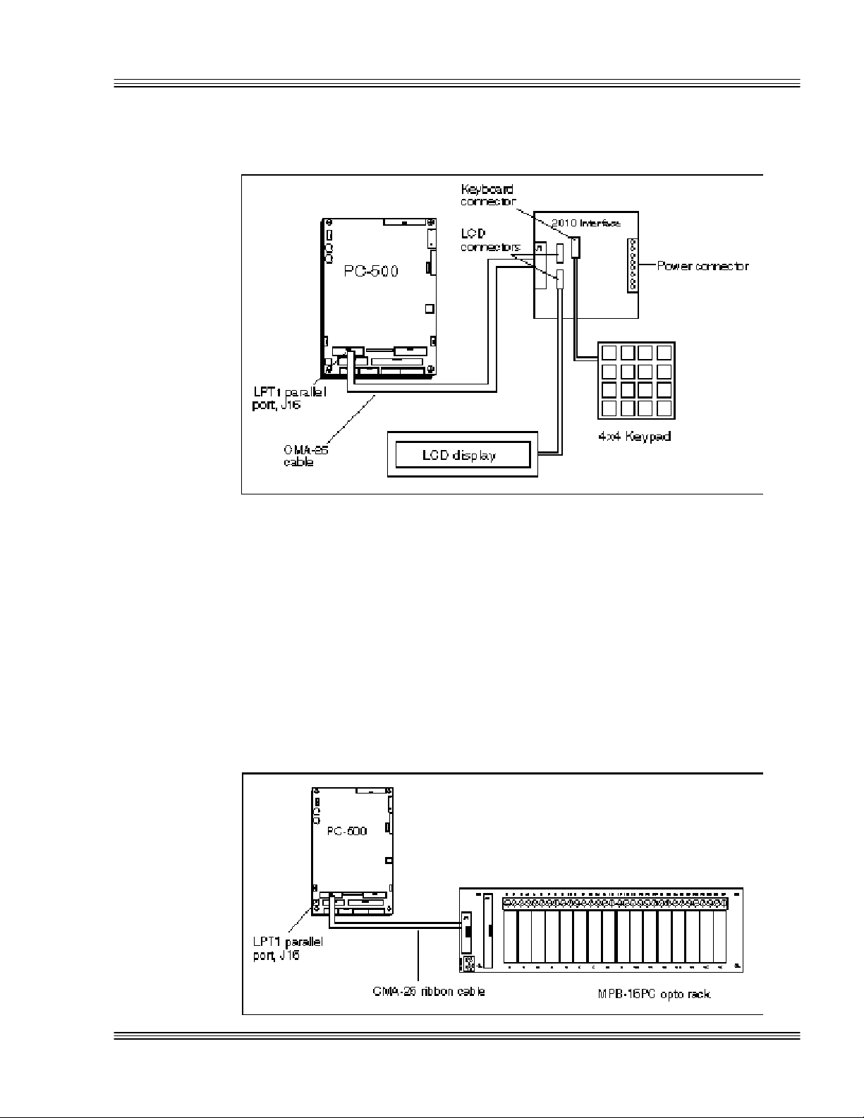
PC-500 user’s manual LPT1 parallel port
Figure 6-2 LPT1 as a display or keypad port
≡ Opto rack
The Octagon MPB-16PC opto rack interfaces directly to the parallel
printer port and can control high voltage/high current G4 opto-isolated
modules. Of the sixteen positions available, eight can be either input or
output, four are dedicated as inputs and the other four are dedicated as
outputs. Refer to the MPB-16PC opto module rack product sheet for
more information.
Figure 6-3 LPT1 and an opto rack
6-3
Page 75

LPT1 parallel port PC-500 user’s manual
6-4
Page 76

PC-500 user’s manual Console devices
Chapter 7: Console devices
≡ Description
The PC-500 has three options for console devices. You can use the onboard video with a monitor and a keyboard as your console. You can also
use COM1 as the console or you can run the system without a console
device.
≡ Selecting console devices
The following represent the PC-500’s three options for console devices:
n Local bus SVGA and a local keyboard. The local bus SVGA can also
drive flat panel displays.
n Serial console from COM1. A serial cable/null modem adapter plugged
into a host PC running SmartLINK provides both input and output.
The local keyboard also allows input.
n No console device means no video output, either from the SVGA moni-
tor or the serial console. The local keyboard allows input.
Local bus SVGA
For correct usage of the CRT and flat panel, see the CRTs and flat panels
chapter.
Serial console
If the serial console is enabled and the video BIOSes are disabled, then
COM1 is used as the console device.
Follow these steps to use the serial console:
1. Power off the PC-500.
2. Connect a VTC-20F to J7 of the PC-500. Refer to Figure 7-1.
3. Connect P2 (COM1 side of the VTC-20F cable) to the 9-pin null modem
adapter. Refer to Figure 7-2.
7-1
Page 77

Console devices PC-500 user’s manual
Figure 7-1 The PC-500 and a serial console
4. If your PC has a 9-pin serial connector, connect the 9-pin null modem
adapter to any serial port (COM1-COM4) on your PC.
5. If your PC has a 25-pin serial connector, attach a 9- to 25-pin adapter to
the 9-pin null modem adapter, and then insert the matching end of the
9- to 25-pin adapter into the serial port.
6. Start PC SmartLINK.
7. Remove W2[1-2] and W3[1-2] to disable the video BIOS.
Note For more information on enabling and disabling the video BIOS, refer to
the following section in this chapter.
8. Power on the PC-500.
Figure 7-2 VTC-20F cable and null modem adapter
7-2
Page 78

PC-500 user’s manual Console devices
Keyboard
You can use any of the console options mentioned in the Selecting console
devices section with a local keyboard.
Speaker
You can also use a local speaker with any of the console options listed
above in the Selecting console devices section. Interface the speaker via a
4-pin connector at J4. You may use any external speaker from 8-50 ohms.
Mouse
You can also add the use of a mouse to the list of serial console devices
mentioned in the Selecting console devices section in this chapter. The
mouse connects to J3 on the PC-500.
Note See the Accessories appendix for mating information on the keyboard,
speaker, and mouse connectors.
≡ Enabling/disabling the video BIOS
The BIOS checks for a video BIOS to determine which console device to
use. If a console device exists, the BIOS will use the console device, the
CRT, or the flat panel. When the console device does not exist, the BIOS
will otherwise use a serial console, if it has not been disabled in SETUP.
To enable/disable the video BIOS area, either change W2[1-2]/W4[1-2] or
run SETUP and change C0000h-C7FFFh or C8000h-CFFFFh ROM
enable options. The jumpers work as a toggle for the SETUP options.
That is, if the SETUP previously shows the BIOS regions as “enabled,”
then changing the state of W2[1-2]/W4[1-2] will disable the regions.
To verify the SETUP program’s state for the C0000h-CFFFFH regions,
remove the USESETUP W2[9-10] and install W2[1-2] and W4[1-2]. This
jumper installation enables the video BIOS areas. To allow for serial
console use, disable the video BIOS areas by removing W2[9-10] and
W2[1-2]/W4[1-2]. See Table 7-1 and Figure 7-3 as reference guides for
disabling and enabling the video BIOS and changing ROM enable.
7-3
Page 79

Console devices PC-500 user’s manual
W4[1–2](V1)
Table 7-1 Video BIOS disabling and enabling options in SETUP
(C0000h-C7FFFh, C8000h-CFFFFh ROM Enable)
Current SETUP
state of
C0000h–C7FFFh,
C8000h–CFFFFh
(ROM Enable)
Disabled On Enabled Change SETUP to
Disabled Off Enabled Change SETUP to
Enabled On Disabled Change SETUP to
Enabled Off Disabled Change SETUP to
Current
jumper state of
W2[1–2](V0)/
W4[1–2](V1)
Desired
state SETUP option
enabled or remove
W2[1–2](V0)/
W4[1–2](V1)
enabled or install
W2[1–2](V0)/
W4[1–2](V1)
disabled or remove
W2[1–2](V0)/
W4[1–2](V1)
disabled or install
W2[1–2](V0)/
Note Octagon strongly recommends that you configure both the ROM Enable
SETUP option and the jumpers, W2[1-2] and W4[1-2] at the same time.
Figure 7-3 Changing ROM Enable flowchart
7-4
Page 80

PC-500 user’s manual Console devices
*= If the SETUP state is unknown, you may need to change W2[1-2]
and W4[1-2] one at a time.
Re-establishing communications when the console is not
working.
If the ROM Enables SETUP state and jumpers W2[1-2]/W4[1-2] were
not configured at the same time, then proceed with Steps A through C:
Step A
1. Remove USESETUP W2[9-10].
2. Install W2[1-2]/W4[1-2].
3. Reboot the system.
If Step A does not work, then follow Step B.
Step B
1. Make sure the BIOS jumper W2[5-6] is on. To use the BIOS in SSD1,
install W2[5-6]. To use the BIOS in SSD0, remove W2[5-6].
2. Reboot the system.
If Step B does not work, then follow Step C.
Step C
1. Remove W2[1-2]/W4[1-2].
2. Attach a serial cable to COM1.
3. Run PC SmartLINK at 9600 baud.
4. Boot the system.
5. Program a new video BIOS if needed.
6. Run SETUP and set the ROM Enable SETUP states accordingly.
7. Re-install the USESETUP jumper W2[9-10].
7-5
Page 81

Console devices PC-500 user’s manual
7-6
Page 82

PC-500 user’s manual SSDs, DRAM, and battery backup
** = W2[7–8] is not jumpered
Chapter 8: SSDs, DRAM, and battery backup
≡ Description
Before you can save and boot your application from the PC-500, you must
first configure the system for your particular application requirements.
≡ SSD0 (optional)
SSD0 is an optional feature and is not installed on the standard version of
the PC-500.
WARNING!
Incorrect installation of SSD0 will destroy the chip. To install
SSD0, be sure to match the notch in the SSD0 chip with the
notch in the SSD0 marked silkscreen on the PC-500.
A flash, SRAM, or EPROM device may be installed on the PC-500.
Jumper blocks W2[7,8] and W5 must be set appropriately. See Table 8-1
for settings.
Selecting SSD0 device type
Table 8-1 SSD0 device selection jumpers: W5, W2[7-8]
Pins Description
W5[1–3, 2–4, 5–7, 8–10] W2[7–8] SRAM with battery backup*
W5[1–2, 3–4, 5–6, 9–10] W2[7–8] Flash
W5[1–2, 3–4, 5–6, 9–10] EPROM**
* = default, pins jumpered
≡ SSD0 replaced with an SRAM device
Before replacing SSD0 with an SRAM device, do the following steps:
1. Power off the PC-500 and then make sure to jumper W2[5-6] is jumpered
in order to boot from the BIOS on SSD1.
2. Since SSD0 is to be replaced with an unprogrammed device, the PC-500
must be configured to boot from SSD1. Run SETSSD.EXE to change the
boot device:
PC500 C:\> SETSSD SSD1 SSD0
8-1
Page 83

SSDs, DRAM, and battery backup PC-500 user’s manual
Use SSD0 BIOS
3. Power off the PC-500 and install a 512K SRAM into SSD0 at socket
U21. Both W5[1-3, 2-4, 5-7, 8-10] and W2[7-8] must be jumpered for an
SRAM device.
Note SRAM contents are sometimes affected by system noise. Therefore, the
use of SRAM is not recommended in electrically noisy environments,
especially when systems are critical.
The SSD0 socket also supports flash and EPROM devices. By default,
SSD0 reserves 192 KB for the system/video BIOS and 320 KB for a
DOS drive. When an SRAM or flash device is used, the DOS drive is
read/writeable through PICO FA. After PFORMAT has run, the
SETSSD/SSD0BIOS option allows the DOS drives on SSD0 to be the
full size, 512 KB.
WARNING!
Alignment of an SRAM, flash, or EPROM device into SSD0 is
critical. Be certain to properly align pin 1 of either the SRAM,
flash, or EPROM device with pin 1 of SSD0 on the PC-500.
≡ SSD0 replaced with a flash device
Before replacing SSD0 with a flash device, do the following steps:
1. Power off the PC-500 and then make sure W2[5-6] is jumpered in order
to boot from the BIOS on SSD1.
2. Since SSD0 is to be replaced with an unprogrammed device, the PC-500
must be configured to boot from SSD1. Run SETSSD.EXE to change
the boot device:
PC500 C:\> SETSSD SSD1 SSD0
3. Power off the PC-500 and install a 512K flash into SSD0 at socket U21.
Both W5[1-2, 3-4, 5-6, 9-10] and W2[7-8] must be jumpered for a flash
device.
Selecting an SSD BIOS
Each SSD may contain a system BIOS and a video BIOS. To select an
SSD BIOS in SSD1, add jumper W2[5-6]. To use SSD0 BIOS, remove
jumper W2[5-6]. See Table 8-2 for the proper settings. To program the
system BIOS/video BIOS, refer to the Managing SSDs chapter.
Table 8-2 Selecting an SSD BIOS: W2[5-6]
8-2
State Result
On Use SSD1 BIOS
Off
Page 84

PC-500 user’s manual SSDs, DRAM, and battery backup
SSD0 replaced with an EPROM/OTPROM
1. Follow steps one through three in the SSD0 replaced with a flash device
section and use a 512K flash.
2. Power off the PC-500 and remove the flash from socket U21.
3. Use an off-card programmer to program a 512K EPROM/OTPROM.
Use the flash as the master copy.
4. Insert the programmed EPROM/OTPROM into socket U21.
5. Remove jumper W2[7-8] for EPROM USE.
6. Power on the PC-500.
7. The new SSD0 device is now ready to be used as a bootable, read-only
DOS drive.
≡ SSD1
Generally, SSD1 is meant for storing the application programs to be
executed on powerup. The programs are automatically loaded into DOS
memory and executed. The standard version of the PC-500 comes with
a 2 MB flash soldered on-board, while the optional version contains a
1 MB flash soldered on-board. Your application programs can be saved
to flash using the PICO FA driver which makes the flash device a read/
write disk on your PC-500. Saving your programs onto the read/write
disk allows you to do this up to 100,000 times, allowing updates to your
application programs. These devices are erased automatically during
the programming process.
SSD1 can be accessed directly as a read/write DOS drive with the PICO
FA driver. Also, it can be accessed directly as a read/write DOS drive
when the PICOFA.SYS driver is loaded. While this is convenient for
product development, the flash, however, has a limited number of writes
allowed. Therefore, Octagon does not recommend SSD1 be used as a
data logging device. Refer to the Software utilities appendix for information on supported flash devices and a description of PICO FA.
≡ DRAM
The standard version of the PC-500 is shipped with 1 MB of DRAM
on-card. The PC-500 can also be configured with 16 MB of surface
mounted DRAM. The on-card DRAM socket holds up to a 32 MB dual
in-line memory module (DIMM). The card supports fast page mode
(FPM) or extended data out (EDO) types of memory. These can be
symmetric or asymmetric configurations. You may order EDO DIMM
memory modules from Octagon Systems. These memory modules,
including a 32 MB version, are also available from third party electronic
component distributors. See the following for ordering information:
Description
4 MB EDO DIMM Octagon 4583
memory module IBM IBM11S1325LPB-70
Manufacturer Manufacturer’s P/N
Kingston KTM1X32V-70DEG
PNY Engineering 321007EDM1G02TB
8-3
Page 85

SSDs, DRAM, and battery backup PC-500 user’s manual
** = W2[7-8] is not jumpered
4 Gnd
8 MB EDO DIMM Octagon 4584
memory module IBM IBM11S2325LPB-70
Kingston KTM2X32V-70DEG
PNY Engineering 322007EDM1G04TB
16 MB EDO DIMM Octagon 4582
memory module IBM IBM11S4325LPB-70
PNY Engineering 324007EDS4G08TL
32 MB EDO DIMM Octagon Call Octagon
memory module
≡ Battery backup for SSD0 SRAM and real time
calendar clock
SSD0 can use 512 KB SRAM by changing W5. Refer to the table below
for the correct pinout listing for the SRAM with battery backup configuration. The SSD0 requires an AT battery for battery backup of the
SRAM files.
An AT battery also backs up the CMOS real time clock.
Table 8-3 SSD0 device configuration: W5, W2[7-8]
Pins Description
W5[1-3, 2-4, 5-7, 8-10] W2[7-8] SRAM with battery backup*
W5[1-2, 3-4, 5-6, 9-10] W2[7-8] Flash
W5[1-2, 3-4, 5-6, 9-10] EPROM**
* = default, pins jumpered
Installing an AT battery
1. Power off the PC-500.
2. Install the 3.6V AT clock battery at the J8 connector. Refer to the
component diagram in the Quick start chapter for the location of J8.
Table 8-4 Battery connector: J8
Pin Function
1 Battery
2 Key
3 Gnd
Note See the Accessories appendix for mating information on the battery
8-4
connector.
Page 86

PC-500 user’s manual External drives
Chapter 9: External drives
≡ Description
The PC-500 is compatible with all common floppy disk drives used on
desktop PCs. The PC-500 also drives any standard IDE or EIDE hard
drives that have 16-bit IDE interfaces. The BIOS extension ROM for
the hard drive is supplied on the card so that no additional software is
needed. The floppy drives use DMA channel 2.
≡ Floppy disk controller
The PC-500 can interface directly to one or two 3.5 in. or 5.25 in. floppy
drives via the connector at J15. Make sure the 34-pin floppy drive cable
meets the following pinout requirements:
Note See the Accessories appendix for mating information on the floppy disk
connector.
Note If you wish to add a second floppy drive to your system, you must use a
floppy drive cable which has two connectors.
Power requirements
The PC-500 requires +5V for operation. You must also supply power to
the floppy drive(s) through an external source. Refer to your floppy
drive manual for specific instructions.
Installing a floppy disk drive
1. Disconnect power to the PC-500.
2. Insert one end of your cable into the rear of the floppy drive. Make sure
pin 1 on the cable is connected to pin 1 on the drive.
3. Insert the other end of the cable into J15 on the PC-500.
4. Connect power to the floppy drive.
5. Run SETUP in the \UTILS subdirectory to setup the AT BIOS. You can
execute this program either by pressing <BACKSPACE><S> during
system bootup or by executing the file SETUP.EXE. This file is found
on the PC-500 BIOS drive and also on the PC-500 utility disk. The
system steps you through the configuration. Also, refer to the SETUP
programs chapter for more information on the AT BIOS SETUP
program.
9-1
Page 87

External drives PC-500 user’s manual
Note If floppy is twisted on the connector, then answer “no” to Swap Floppy
A and B.
≡ Hard disk controller
The PC-500 will drive up to 4 gigabytes hard drives that have 16-bit
IDE interfaces via a 44-pin connector at J18. Make sure your cable
meets the pinout requirements of the following table:
Note See the Accessories appendix for mating information on the IDE hard
connector.
Installing a hard drive:
1. Disconnect power to the PC-500.
2. Insert one end of the Octagon hard drive adapter cable into the rear of
the hard drive. Make sure pin 1 on the cable is connected to pin 1 on
the drive.
3. Insert the other end of the IDE cable into J18 on the PC-500. Make
sure pin 1 on the cable is connected to pin 1 on the PC-500.
4. Execute the BIOS SETUP program to configure your system for a hard
drive. You can execute this program either by pressing <BACKSPACE><S> during system bootup or by executing the file
SETUP.EXE. This file is found on the PC-500 BIOS drive and the
PC-500 utility disk. The system steps you through the configuration.
Also, refer to the SETUP programs chapter for more information on the
BIOS SETUP program.
5. If you want to boot the system from the hard drive, you need to format
the drive accordingly.
≡ Booting with ROM-DOS
If you want to boot from a floppy/hard drive with ROM-DOS, do the
following steps:
1. Boot from the PC-500 utility disk.
2. Execute the following command:
9-2
SYS C:
3. The system copies COMMAND.COM as well as a hidden file to the hard
drive.
Page 88

PC-500 user’s manual IRQ routing and opto IRQs
Chapter 10: IRQ routing and opto IRQs
≡ Interrupt routing
The PC-500 provides a flexible method of enabling, disabling, and
routing system interrupts via an “in system” programmable logic device.
The logic device not only reduces the number of physical jumpers, but it
also reduces the possibility of choosing the incorrect jumper configuration. For example, upon configuration the electronic jumpers remain set
until they are reprogrammed for a different configuration.
This device also allows some of the PC/104 bus interrupts and some of
the on-board generated interrupts to be routed to other IRQs of the
programmable interrupt controller. This routing matrix requires the
user to run the SETIRQ utility program to update the routing matrix
with the desired IRQ routes.
In addition to IRQ routing, the I/O range select A and select B bits can
be set so that the base addresses in COM5, EZ I/O, and COM3 through
COM5 IRQ status registers can be moved to different locations. These
can also be read at I/O address 0A9h bits 4 and 5.
See also the SETIRQ.DOC file in the \IRQ directory on the PC-500
utility disk for more information. The utility disk contains several ISP
files to program into the matrix. If these are not sufficient, call
Octagon’s Technical Support at 303-426-4521 for new ISP files that may
have become available.
Note If an output is not routed as a signal, then the output or destination is
neither driven high nor low, but is in a high impedance mode.
Note When you program a new IRQ routing matrix, the printer port must be
set to bi-directional mode. Also, any field devices connected to the
printer port must be disconnected.
10-1
Page 89

IRQ routing and opto IRQs PC-500 user’s manual
Figure 10-1 Interrupt routing matrix
10-2
Page 90

PC-500 user’s manual IRQ routing and opto IRQs
≡ Opto IRQs
OPTOA and OPTOB are the two optically isolated channels and are
accessible at J10. These channels are configurable to drive either the
SUSPEND/RESUME or the PMI signal. Also, either OPTOA or OPTOB
can be routed through the interrupt routing matrix to generate a system
reset. The opto-isolation allows the input source to extend as far as
50 feet from the card. A +5V signal activates the SUSPEND/RESUME,
PMI or system reset signal. Noise filtering is built-in and the isolation
from the system ground is 500V. A voltage greater than 3.1V at 5.0 mA
guarantees a SUSPEND/RESUME or a PMI interrupt or a system
reset.
When signaling for SUSPEND/RESUME, PMI, or system reset, the
voltage is applied in a pulse period greater than 50 µS. The interrupt
matrix chip requires that the input voltage remains stable until the
interrupt is acknowledged. At that time, the interrupt source can be
rearmed by returning the input to 0 volts.
Note See the Accessories appendix for mating information on the OPTOA and
OPTOB connectors.
The interrupt routing matrix provides flexibility to the interrupt struc-
ture which allows connection between the lower-ordered ISA interrupts
and the unused higher-ordered interrupts. Caution must be used when
configuring the jumper options.
Note Bus IRQ6 can be inadvertently routed to two interrupts. This is not an
acceptable configuration. The application software must also be aware
of the interrupt that is set for the particular resource.
≡ Interrupt routing matrix defaults
The 500_001.ISP file lists the interrupt routing matrix defaults. See
the SETIRQ.DOC file on the PC-500 utility disk for more information.
≡ Programming
SETIRQ 500_001.ISP
See the \IRQ\SETIRQ.DOC directory on the PC-500 utility disk for
additional PC-500 ISP files and their functional descriptions in the
SETIRQ.DOC file.
≡ Master disable
When W4[9-10] is jumpered, the outputs from the interrupt matrix chip
10-3
Page 91

IRQ routing and opto IRQs PC-500 user’s manual
* = default
are tri-stated (high). The chip does not program when this jumper is
installed.
I/O range select can be adjusted via ISP files and SETIRQ. The I/O
range select changes the EZ I/O, COM5 base addresses. See
SETIRQ.DOC for more information.
The IORG SEL A (I/O register select A) and IORG SEL B (I/O register
select B) select the base address for COM5, as well as for the EZ I/O and
the interrupt status register.
Table 10-1 Interrupt status port (ISP) map setting at I/O location 0A9h
I/O range select
A (bit 5) B (bit 4)
0 0 140-147h 150-157h 158-15Fh
0 1 120-127h 130-137h 138-13Fh
1 0 340-347h 350-357h 358-35Fh
1* 1* 320-327h* 330-337h* 338-33Fh*
COM5
addresses
EZ I/O
addresses
Interrupt status
port addresses
10-4
Page 92

PC-500 user’s manual EZ I/O
Chapter 11: EZ I/O
≡ Description
Octagon EZ I/O digital I/O lines can be used to sense switch closures,
turn on lamps and LEDs, and interface with other devices that have TTL
input or output such as printers and scales. The EZ I/O drives the
Octagon MPB series opto-isolation module racks directly, controlling AC
and DC loads to 240V at 3A. Figure 11-1 shows typical EZ I/O configurations. The EZ I/O port at J11 has the following features:
n The EZ I/O chip has 24 I/O lines, grouped into 3 ports of 8 bits
n Each bit is programmable as either 5V input or 5V output
n Read back state of each pin
n Easy-to-program
n Sink and source 15 mA
Figure 11-1 Typical EZ I/O configurations
11-1
Page 93

EZ I/O PC-500 user’s manual
Gnd
* = default
Table 11-1 EZ I/O connector: J11
Pin Function Pin Function Pin Function
Port A
19
21 bit 1 8 bit 1 16 bit 1
23 bit 2 4 bit 2 15 bit 2
25 bit 3 6 bit 3 17 bit 3
24 bit 4 1 bit 4 14 bit 4
22 bit 5 3 bit 5 11 bit 5
20 bit 6 5 bit 6 12 bit 6
18 bit 7 7 bit 7 9 bit 7
bit 0 10
Port B
bit 0 13
2 +5V safe
26
Port C
bit 0
Note See the Accessories appendix for mating information on the EZ I/O
connector.
≡ Pulling the I/O lines high or low
Jumper block W3 pulls the I/O lines at ports A, B, and C high or low.
This allows a known state upon powerup. The default configuration
pulls all of the I/O lines high. Note that 10K ohm resistor networks are
used to configure the I/O lines as high or low.
Table 11-2 EZ I/O pull-up/pull-down jumpers: W3
Pins Label Description
[1–2]* Pull up to +5V
[2–4] Pull down to Gnd
[9–10]* UA User option jumper A
≡ Organization of ports
The EZ I/O digital port has a total of 24 I/O lines connected to a 26-pin
header. The lines are configured into three groups: ports A, B and C,
each group consisting of 8 bits. Any of the lines at ports A, B, or C can
be configured individually as inputs or outputs.
11-2
Page 94

PC-500 user’s manual EZ I/O
Control register Base address + 3
Figure 11-2 Organization of ports
Port addressing
Ports A, B, C and the control register are addressable.
Table 11-3 EZ I/O port address
Port I/O address
A Base address
B Base address + 1
C Base address + 2
Base I/O address
The base I/O address for the EZ I/O port is 330h (default). This address
can be changed through OctaGlue PCS_2 to one of four addresses.
Refer to the section Interrupt routing in the IRQ routing and opto IRQs
chapter to change the base address of the EZ I/O chip.
Based on the I/O range select A and B, you can determine the port
addresses for the EZ I/O port by reading 0A9h bit 4 and 0A9h bit 5.
Refer to Table 11-4.
11-3
Page 95

EZ I/O PC-500 user’s manual
* = default
Table 11-4 Reading the EZ I/O port
I/O range select A
(bit 5)
0 1 130h
0 0 150h
1 1 330h*
1 0 350h
I/O range select B
(bit 4)
EZ I/O
base address
≡ Configuring and programming the EZ I/O ports
Located at J11 on the PC-500, the digital I/O connector is programmable by an Octagon EZ I/O digital chip. The EZ I/O chip has three
ports with eight parallel I/O lines (bits) per port. This port can use one
of four base I/O addresses. All lines can be individually programmed as
all inputs, all outputs, or individually as inputs or outputs. You can
alter which bits are inputs or outputs by writing a control command to
the control register of the EZ I/O port. When a line is configured as an
output, it can sink a maximum of 15 mA at 0.4V or can source 15 mA at
2.4V. On powerup and software or hardware reset, all digital I/O lines
at J11 reset as inputs.
Programming the EZ I/O
Follow these steps to program the EZ I/O chip:
1. Configure the EZ I/O port bit directions, either as inputs or outputs.
2. Write to port A, B, or C with the desired level or read the bit level from
the desired port.
Configuring the EZ I/O
Follow these steps to configure the EZ I/O chip
1. Write a "2" to the control register (base address + 3). This places
the I/O chip in “direction” mode:
(default base address = 330h)
OUT 333h, 2 (control register, direction mode)
2. Set the direction of each bit. A "0" written to the corresponding line
indicates an input and a "1" bit indicates an output. Each bit corresponds to the equivalent I/O line.
11-4
Page 96

PC-500 user’s manual EZ I/O
x
Table 11-5 EZ I/O port byte
EZ I/O port
bit 7 bit 6 bit 5 bit 4 bit 3 bit 2 bit 1 bit 0
x 7
x 6
x 5
x 4
x 3
x 2
x 1
I/O line
0
For example, writing 00011100 to port C (base address + 2) will configure port C I/O lines 0, 1, 5, 6, and 7 to be inputs and lines 2, 3, and 4 to
be outputs:
OUT 332h, 1Ch (00011100 binary = 1C hexadecimal)
3. Write a "3" to the control register (base register+3). This places the I/O
chip back into “operation” mode:
OUT 333h, 3 (control register)
Writing and reading from EZ I/O
Writing to or reading from the desired EZ I/O port is accomplished with
single program statements:
1. To write a bit pattern to the desired EZ I/O port:
OUT 332h, FFh
All bits of port C go high; all input bits are unaffected.
2. To read a bit pattern from the desired EZ I/O port:
PORTC = INP(332h)
The byte read from port C is assigned to variable port C.
EZ I/O output program examples
To configure ports A, B, and C as all outputs, issue the commands:
OUT 333h, 2 ‘Direction’ Mode
OUT 330h, FFh ‘PortA’
OUT 331h, FFh ‘PortB’
OUT 332h, FFh ‘PortC’
OUT 333h, 3 ‘Operation’ Mode
11-5
Page 97

EZ I/O PC-500 user’s manual
Note With CAMBASIC, Octagon’s multitasking industrial language, you can
also accomplish the same configuration and outputs with one statement.
Enter:
CONFIG EZ I/O &330, &0, &FF, &0, &FF, &0, &FF
Ports A, B, and C will now output all "1"s after issuing the following
commands:
OUT 330h, FFh (portA)
OUT 331h, FFh (portB)
OUT 332h, FFh (portC)
or all "0"s after:
OUT 330h, 0 (portA)
OUT 331h, 0 (portB)
OUT 332h, 0 (portC)
EZ I/O input program examples
To configure ports A and C as inputs and port B as outputs, issue the following commands:
OUT 333h, 2 'Direction Mode'
OUT 330h, 0
OUT 331h, FF
OUT 332h, 0
OUT 333h, 3 'Operation Mode'
To read ports A and C, issue the following commands:
PORTA = INP(330h) (port A)
PORTC = INP(333h) (port B)
≡ Enhanced INT 17h function definitions
This section provides definitions for the following functions: Initialize
EZ I/O, Write EZ I/O, and Read EZ I/O.
Initialize EZ I/O
Function: efh
Subfunction: 00h
Purpose: To set the directions and to program the initial
values of an EZ I/O port.
11-6
Calling registers:
AH efh
AL 00h
DI Port A configuration
xxxxxxxx xxxxxxxxB
xxxxxxx Initial data for port A
Page 98

PC-500 user’s manual EZ I/O
xxxxxxxxB direction; 1->output, 0->input
BX Port B configuration
xxxxxxxx xxxxxxxxB
xxxxxxxx Initial data for port B
xxxxxxxxB direction; 1->output, 0->input
CX Port C configuration
xxxxxxxx xxxxxxxxB
xxxxxxxx Initial data for port C
xxxxxxxxB direction; 1->output, 0->input
DX ffffh
Return registers: Carry flag cleared if successful
Carry flag set if error
AL Error code
Comments: This function is used to initialize the EZ I/O before normal
use.
Programming example:
/* Inline assembly code for Borland C++ 3.1 */
asm {
mov ax,0ef00h
mov di,00ffh /*port A all outputs, init data=all 0’s */
mov bx,55ffh /*port B all outputs, init data=55h*/
mov cx,0000h /*port C all inputs*
mov dx,0ffffh
int 17h
}
Write EZ I/O
Function: efh
Subfunction: 01h
Purpose: To write a value of an EZ I/O port.
Calling registers:
AH efh
AL 01h
DI Port A mask and data
xxxxxxxx xxxxxxxxB
xxxxxxxx Mask for port A; 1->bit to be changed
xxxxxxxxB Data for port A
BX Port B mask and data
xxxxxxxx xxxxxxxxB
xxxxxxxx Mask for port B; 1->bit to be changed
xxxxxxxxB Data for port B
CX Port C mask and data
xxxxxxxx xxxxxxxxB
xxxxxxxx Mask for port C; 1->bit to be changed
xxxxxxxxB Data for port C
DX ffffh
11-7
Page 99

EZ I/O PC-500 user’s manual
Return registers: Carry flag cleared if successful
Carry flag set if error
AL Error code
Comments: This function is used to initialize the EZ I/O before normal
use.
Programming example:
/* Inline assembly code for Borland C++ 3.1 */
asm {
mov ax,0ef01h
mov di,00ffh /*port A: no change */
mov bx,8000h /*port B: bit 7=0, other bits unchanged*/
mov cx,0202h /*port C: bit 1=1, other bits unchanged*
mov dx,0ffffh
int 17h
}
Read EZ I/O
Function: efh
Subfunction: 02h
Purpose: To read from an EZ I/O port.
Calling registers:
AH efh
AL 01h
xxxxxxxx Data for port C
DX ffffh
Return registers: Carry flag cleared if successful
AL Port A data
AH Port B data
BL Port C data
Carry flag set if error
AL Error code
Comments: This function is used to read from the EZ I/O before nor-
mal use.
Programming example:
/* Inline assembly code for Borland C++ 3.1 */
unsigned char aData, bData, cData;
asm {
mov ax,0efoch
mov dx,0ffffh
int 17h
mov aData,al
mov bData,ah
mov cData,bl
}
11-8
Page 100

PC-500 user’s manual EZ I/O
≡ Opto-module rack interface
You can interface digital I/O lines to an 8-, 16-, or 24-position opto-module
rack. One end of the CMA-26 cable plugs into the EZ I/O connector and the
other plugs into an MPB-8, MPB-16, or an MPB-24 opto rack. Refer to the
MPB opto racks data sheet for more information.
You can also use a CMA-26 cable to connect the EZ I/O port to an STB-26
terminal board and then to the opto rack. The STB-26 has two 26-pin
connectors, one of which would connect to the EZ I/O port, the other would
connect to the opto rack. Refer to the following opto rack diagrams.
For either configuration, run a separate power line to +5V and ground on
the opto-rack.
Figure 11-3 MPB-16PC opto rack hookup
11-9
 Loading...