O2Micro OZ6833T, OZ6833B Datasheet

FEATURES
• Single-chip CardBus host adapter
• Supports 2 PCMCIA 1.0 and JEIDA 4.2 R2 cards or 2
CardBus cards
• ACPI-PCI Bus Power Management Interface
Specification Rev1.0 Compliant
• Supports OnNow LAN wakeup, OnNow Ring Indicate,
PCI CLKRUN#, PME#, and CardBus CCLKRUN#
• Compliant with PCI specification v2.1S, 1998 PC Card
Standard 7.0
• Yenta PCI to PCMCIA CardBus Bridge register
compatible
• ExCA (Exchangeable Card Architecture) compatible
registers map-able in memory and I/O space
• Intel 82365SL PCIC Register Compatible
• Supports PCMCIA_ATA Specification
• Supports 5V/3.3V PC Cards and 3.3V CardBus cards
• Supports two PC Card or CardBus slots with hot
insertion and removal
• Supports multiple FIFOs for PCI/CardBus data transfer
• Supports Direct Memory Access for PC/PCI and
PC/Way on PC Card socket
• Programmable interrupt protocol: PCI, PCI+ISA,
PCI/Way, or PC/PCI interrupt signaling modes
• Win’98 IRQ and PC-97/98 compliant
• Parallel or Serial interface for socket power control
devices (TI or Micrel)
• Zoomed Video Support
• Integrated PC 98 – Subsystem Vendor ID support, with
auto lock bit
• LED Activity Pins
ORDERING INFORMATION
OZ6833T – 208 pin TQFP
OZ6833B – 208 pin Mini-BGA
GENERAL DESCRIPTION
The OZ6833 ACPI CardBus controller provides a high
performance, synchronous, 32-bit, bus master/target
interface between computers and plug in PC Cards.
CardBus is the new 32-bit interface standard of Personal
Computer Memory Card International Association,
PCMCIA. The CardBus provides 32-bit interface with
multiplexed address and data lines. This will allow the
addition of high performance computer system
enhancements and new functions in a user-friendly way.
Further, the expansion capability of the CardBus will
provide benefits to the end user. CardBus is intended to
OZ6833
ACPI CardBus Controller
support “temporal” add-in functions on PC Cards, such as
Memory cards, Network interfaces, FAX/Modems and other
wireless communication cards, etc. The high performance
and capability of the CardBus interface will enable further
development of many new functions and applications.
The OZ6833 CardBus controller is a 33MHz PCI compliant
master/target device that attaches to the PCI bus and
manages two PC Card sockets. The PC Card sockets
support both 3.3V / 5V versions of 8/16-bit PCMCIA R2
card or 32-bit CardBus card. R2 card support is compatible
with the Intel 82365SL PCIC controller. CardBus card
support is fully compatible with the 1998 PC Card Standard
V7.0. The OZ6833 is a stand alone device. It does not
require an additional buffer chip for the two PC Card socket
interface. The OZ6833 is implemented with a complex
multiple FIFO data buffer for the PCI and CardBus interface
to provide better PCI/CardBus access.
The FIFO buffers allow the bridge to accept data from a
target bus while moving data to it, facilitating deadlock
prevention. In addition, the OZ6833 is designed with
dynamic PC Card hot insertion and removal and auto
configuration capabilities.
The OZ6833 ACPI CardBus Controller provides the power
saving mixed 5V / 3.3V capability. An advance CMOS
process minimizes system power consumption. The dev ice
also provides a power-down mode, allowing host software
to reduce power consumption further while stopping
internal clock distribution and the clocks on PC Card
sockets. The OZ6833 is not only a CardBus bridge, but
also a socket controller. The OZ6833 supports two master
devices and arbitrates the priority of each. Further, it
supports inter CardBus direct data transfer. The register set
in the OZ6833 is the superset of the OZ67xx register set,
assuring full compatibility with existing socket/card-services
software and PC-card applications. The OZ6833 provides
the most advanced design flexibility for the PC Card
interface in notebook computer design.
To enhance the performance between the PCI bus and any
CardBus card, two buffers (each composed of 16 double
words) are added on both sides going from PCI to CardBus
or the other way around. By implementing these buffers,
the OZ6833 will not refuse data from a target bus while
moving data and preventing deadlock situations.
In order to allow maximum flexibility for system designers,
the CINT# of the PC card 32-bit may be programmed to
steer to either INTA# or INTB# of the PCI bus. Further, the
interrupts may be programmed to route through the bridge
to either PCI INT lines or IRQ interrupts on the ISA bus.
04/25/00 OZ6833-DS-1.55 Page 1
Copyright 1999 by O2Micro All Rights Reserved

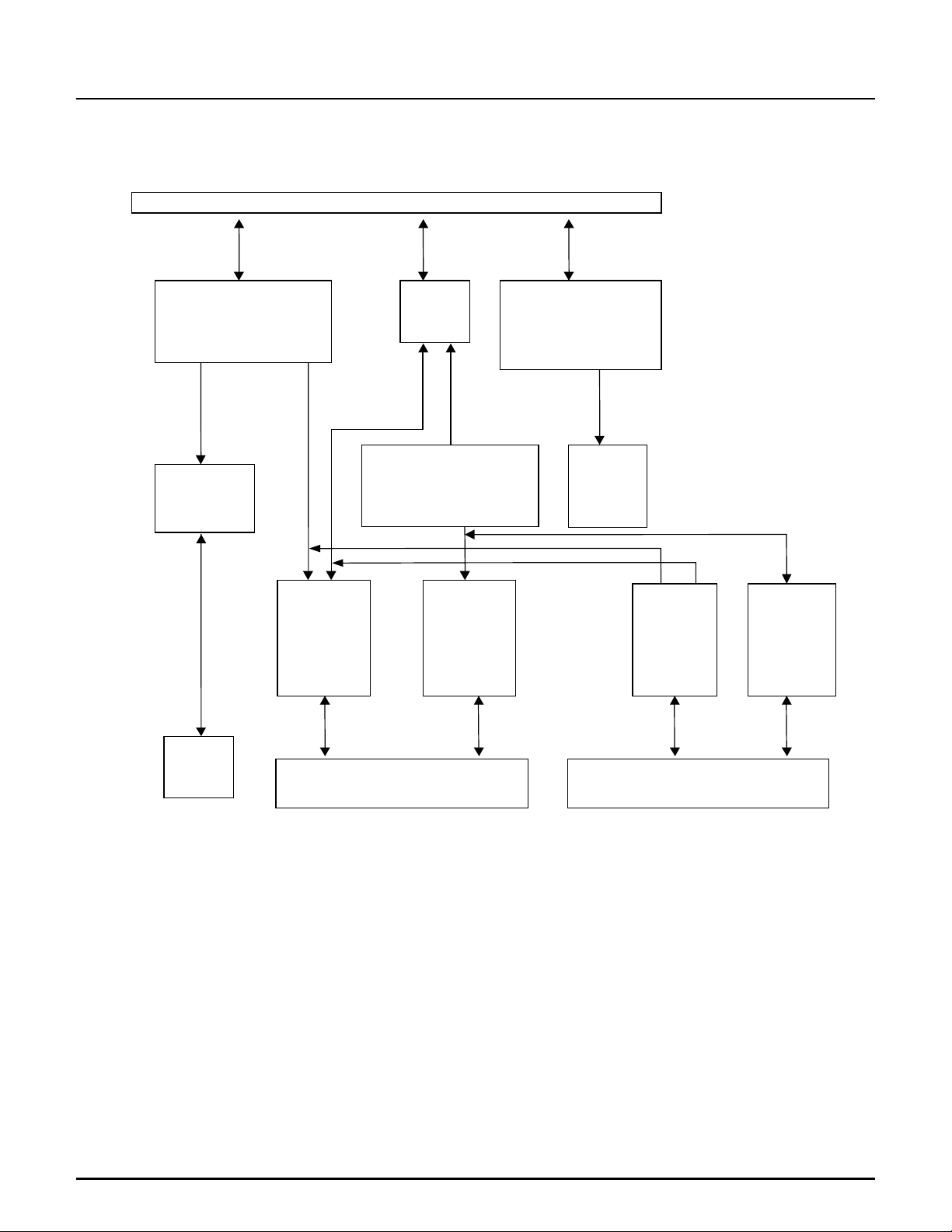
FUNCTIONAL BLOCK DIAGRAM
PCI Interface
OZ6833
PCI Configuration/
Function Control Registers
Power Switch
Control
PCI
Function Control
Configuration/
Registers
Power
Contro
Switch
l
PC Card
Machine
EXCA
8/16-Bit
16-
PC
Bit
Machin
Card
State
e
PCI
PCI
Arbite
Arbiter
r
CardBus FIFO
CardBu
Data Buffering
s
CardBus
PC Card
State
Machine
and
Arbiter
FIFO
ACPI/ OnNow
Power Management
for PC99
Interrupt
Subsystem
Interrup
t
EXCA
8/16 Bit
PC Card
State
Machine
CardBus
PC Card
State
Machine
and
Arbiter
Powe
Power
Switc
r
Switch
h
Interface
Socket A PC Card Interface
PC Card
Interface
Socket B PC Card Interface
OZ6833-DS-1.55 Page 2

OZ6833
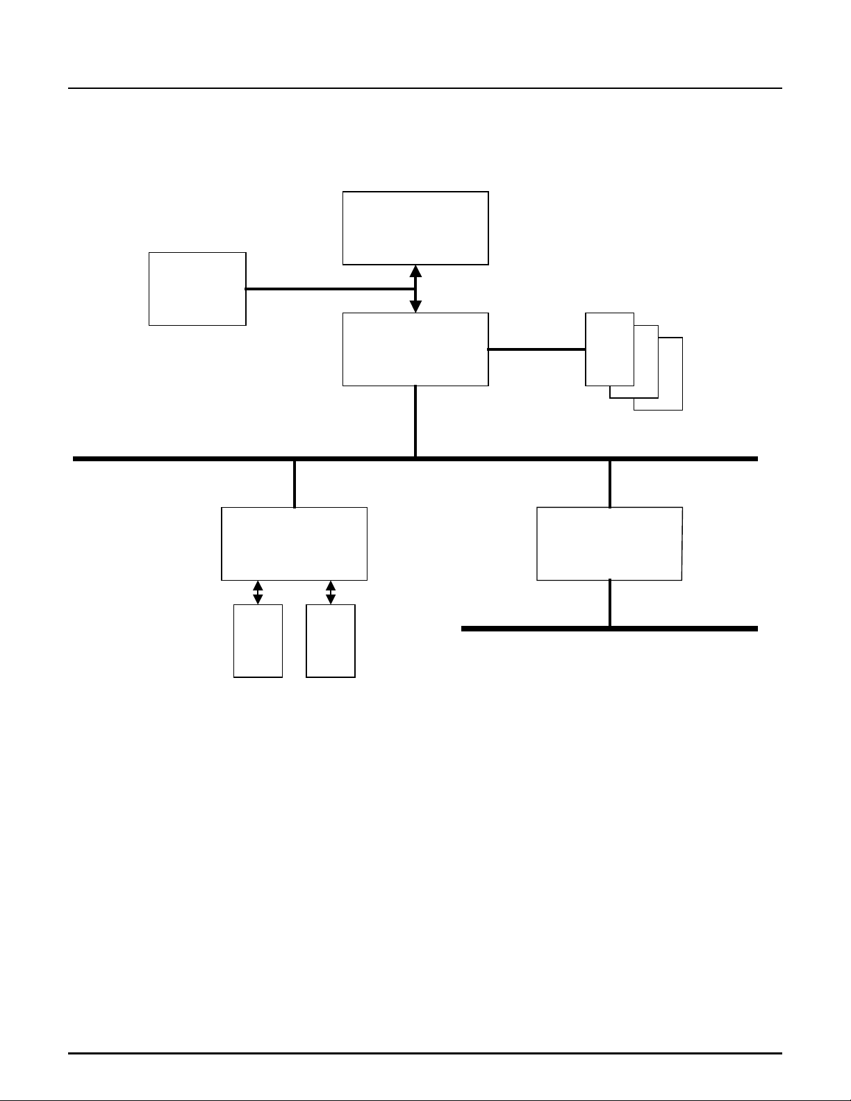
SYSTEM BLOCK DIAGRAM
The following diagram is a typical system block diagram utilizing the OZ6833 ACPI CardBus controller with other related
chipsets.
CPU
PCI Bus
VGA
AGP
OZ6833
CardBus
Controller
PC
Card
PC
Card
Memory
North Bridge
South Bridge
ISA
OZ6833-DS-1.55 Page 3

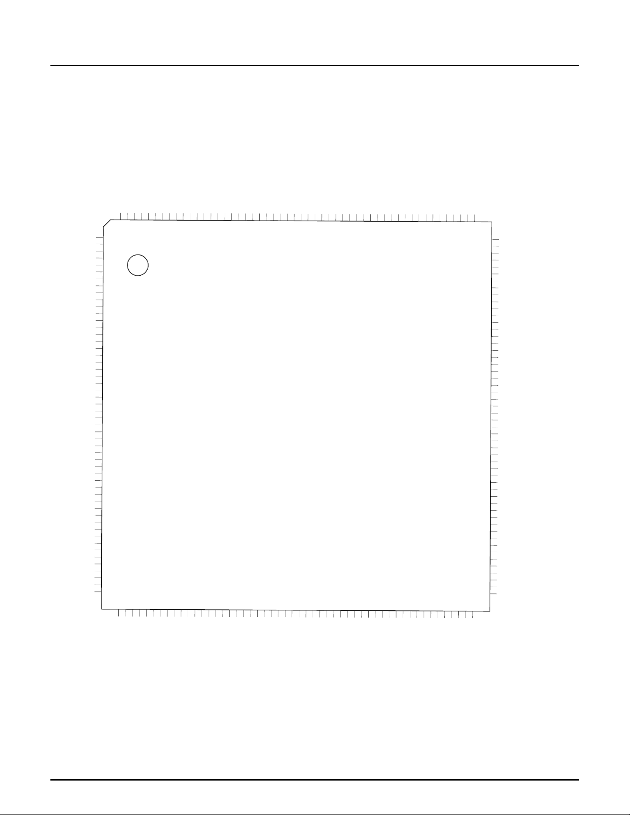
PIN DIAGRAM - 208 PIN TQFP
OZ6833
IRQ7/SIN#/B_VPP_PGM
B_RESET/CRESET#
B_WP/CCLKRUN#
IRQ14/CLKRUN#
IRQ5/SERIRQ
RST#
2
2
2
2
0
0
0
P
C
K
C
I
L
_
N
P
C
G
I
_
#
T
P
C
I
_
R
#
E
Q
A
D
3
1
A
0
D
3
P
C
I
_
V
C
C
A
D
2
9
A
8
D
2
A
7
D
2
A
D
2
6
A
5
D
2
4
A
D
2
C
#
/
B
E
3
R
C
E
_
O
N
D
G
I
D
S
E
L
A
D
3
2
A
2
D
2
A
1
D
2
A
D
0
2
A
9
D
1
P
C
I
V
C
C
_
A
D
8
1
7
A
D
1
6
A
D
1
C
#
/
B
E
2
R
C
E
O
N
G
D
_
R
F
A
E
#
M
G
R
C
E
_
O
N
D
I
R
D
Y
#
R
T
D
Y
#
D
E
V
S
E
L
#
P
O
S
T
#
P
E
R
R
#
S
E
R
R
#
P
A
R
C
/
B
#
E
1
P
C
V
C
I
C
_
5
A
D
1
A
D
1
4
A
3
D
1
2
A
D
1
A
D
1
1
A
0
D
1
R
C
O
N
D
G
E
_
A
D
9
A
D
8
C
/
B
E
#
0
A
D
7
A
D
6
P
C
I
_
V
C
C
A
D
5
A
D
4
0
1
7
6
5
8
2
3
4
5
6
7
8
9
0
1
1
1
2
1
3
1
1
4
5
1
6
1
7
1
8
1
9
1
0
2
1
2
2
2
3
2
4
2
5
2
6
2
7
2
8
2
9
2
0
3
1
3
2
3
3
3
4
3
5
3
6
3
7
3
8
3
9
3
0
4
1
4
2
4
4
3
4
4
5
4
4
6
7
4
8
4
4
9
0
5
1
5
5
2
5
5
5
5
3
6
5
4
B_SOCKET_VCC
B_CD2#/CCD2#
IRQ4/INTB#
2
0
4
5
5
7
8
B_D10/CAD31
B_D2/RFU
INTA#
2
2
2
2
1
0
3
5
9
1
0
0
0
9
9
2
1
0
9
8
6
6
6
6
6
0
1
2
3
4
IRQ11/SKTB_ACTV
B_BVD1/CSTCHG
B_D0/CAD27
B_D8/CAD28
B_D1/CAD29
B_D9/CAD30
1
1
9
9
7
6
6
6
6
5
B_A0/CAD26
1
1
1
1
1
9
9
9
9
9
5
4
3
2
1
6
6
6
7
7
8
9
0
B_INPACK#/CREQ#
B_REG#/CC_BE3#
B_BVD2/CAUDIO
B_A1/CAD25
1
1
9
8
0
9
7
7
2
1
B_WAIT#/CSERR#
B_A2/CAD224
B_A3/CAD23
1
1
1
1
1
8
8
8
8
8
8
7
6
5
4
O
M
i
2
O
Z
7
7
7
7
7
3
4
6
5
7
8
B_VS2/CVS2
B_A6/CAD20
B_A5/CAD21
B_A4/CAD22
CORE_VCC
GND
1
1
1
1
1
1
8
3
r
c
6
7
7
9
1
8
8
8
7
7
2
o
8
8
0
7
1
0
9
8
7
,
I
.
c
n
3
3
8
8
8
8
8
1
2
3
4
5
B_A23/CFRAME#
B_A12/CCBE2#
B_A24/CAD17
B_A25/CAD19
B_A7/CAD18
1
1
1
1
1
7
7
7
7
7
6
5
4
3
2
8
8
8
8
9
6
7
8
9
0
B_RDY_IREQ#/CINT#
B_A21/CDEVSEL#
B_A20/CSTOP#
B_A22/CTRDY#
B_A15/CIRDY#
1
1
7
7
0
1
9
1
B_WE#/CGNT#
B_A16/CCLK
1
1
1
1
1
6
6
6
6
6
9
8
7
6
5
9
9
9
9
9
4
2
3
6
5
B_SOCKET_VCC
B_A19/CBLOCK#
B_A14/CPERR#
IRQ12/PME#
1
1
1
6
6
6
4
3
2
1
9
9
9
0
8
7
9
0
B_A8/CCBE1#
B_A17/CAD16
B_A13/CPAR
B_A18/RFU
1
1
1
1
1
6
6
5
5
5
6
5
1
1
0
9
8
7
5
1
5
1
5
1
5
1
5
1
5
1
4
1
4
1
4
1
4
1
4
1
4
1
4
1
4
1
4
1
4
1
3
1
3
1
3
1
1
3
3
1
3
1
1
3
3
1
3
1
1
3
2
1
2
1
1
2
2
1
2
1
1
2
2
1
2
1
2
1
2
1
1
1
1
1
1
1
1
1
1
1
1
1
1
1
1
1
1
1
1
1
0
1
0
1
0
1
0
1
1
1
1
1
0
1
0
0
0
0
4
1
2
3
I
O
B
_
W
/
R
C
#
A
5
D
5
B
A
_
4
I
O
B
_
3
A
B
_
2
B
V
_
1
O
B
_
0
C
B
_
9
B
A
_
8
D
B
_
7
C
B
_
6
B
V
_
5
D
B
_
4
D
B
_
3
B
S
_
2
D
B
_
1
D
B
_
0
D
B
_
9
D
B
_
8
B
_
D
7
D
B
_
6
C
B
_
5
B
_
D
4
R
C
O
3
E
D
L
2
S
C
L
1
S
D
A
0
A
S
L
9
C
O
R
8
S
P
K
7
A
U
X
6
A
_
C
5
W
A
_
4
D
A
_
3
A
D
_
2
D
A
_
1
D
A
_
0
A
D
_
9
D
A
_
8
B
A
_
7
A
S
_
6
A
A
_
5
V
A
_
4
A
B
_
3
A
A
_
2
R
A
_
1
A
A
_
0
I
N
A
_
9
A
A
_
3
8
A
W
_
7
A
4
A
_
6
R
A
_
5
A
A
5
_
1
/
C
9
A
D
4
1
R
D
/
C
#
A
D
1
3
/
C
1
A
D
1
1
2
/
S
C
1
V
S
1
E
#
/
C
1
A
D
1
/
C
#
A
D
E
2
0
1
/
C
0
A
1
D
9
5
1
/
C
A
D
8
/
C
#
C
E
1
#
B
E
0
V
P
P
_
C
C
4
1
/
R
U
F
/
C
7
A
D
7
C
O
K
E
V
C
C
_
T
3
1
/
C
A
D
6
/
C
6
A
D
5
/
C
2
1
A
D
4
/
5
C
A
D
3
/
C
1
A
D
1
2
/
C
4
A
D
1
D
/
C
#
C
1
D
1
#
/
C
3
A
D
0
V
E
_
C
C
_
U
/
T
S
O
K
T
A
C
I
_
T
V
I
Y
V
K
C
/
A
_
A
/
T
B
V
_
T
C
H
/
B
_
N
G
E
_
D
O
R
_
U
T
_
V
C
C
/
C
#
D
C
2
P
/
C
K
C
L
1
/
C
0
A
D
/
R
U
2
F
/
C
9
A
D
3
/
C
1
A
D
2
/
C
8
A
D
2
/
C
0
A
D
2
V
/
D
S
S
T
1
C
K
O
E
_
T
/
C
0
A
6
D
2
V
C
P
P
C
_
/
V
D
C
2
A
/
C
1
5
A
D
2
/
C
#
C
E
G
/
C
2
A
D
4
2
P
A
C
K
#
/
C
3
A
D
2
A
I
#
T
/
C
S
/
C
A
2
D
2
E
/
S
E
T
C
/
C
A
D
1
2
T
#
C
5
C
#
C
3
V
C
#
5
C
_
#
#
D
2
R
U
N
#
1
3
0
9
8
7
C
H
G
V
C
C
U
D
I
O
B
#
E
3
/
C
R
#
E
Q
E
R
R
#
R
E
#
S
E
T
AD0
AD3
AD2
AD1
CORE_GND
LOCK#
A_D3/CAD0
A_SOCKET_VCC
A_CD1#/CCD1#
A_D4/CAD1
A_D11/CAD2
A_D5/CAD3
A_D12/CAD4
A_D6/CAD5
A_D13/CAD6
A_D7/CAD7
A_D14/RFU
A_CE1#/CCBE0#
A_D15/CAD8
IRQ15/RING_OUT
A_A10/CAD9
A_CE2#/CAD10
A_OE#/CAD11
A_VS1/CVS1
A_A11/CAD12
A_IORD#/CAD13
CORE_VCC
A_A9/CAD14
A_IOWR/CAD15
A_A8/CCBE1#
A_A17/CAD16
A_A13/CPAR
A_A18/RFU
A_A14/CPERR#
IRQ3/VCC3#
A_A19/CBLOCK#
A_WE#/CGNT#
A_A20/CSTOP#
A_RDY_IREQ#/CINT#
A_A21/CDEVSEL#
A_A16/CCLK
A_A22/CTRDY#
A_A15/CIRDY#
A_A23/CFRAME#
A_A12/CCBE2#
SOCKET_VCC
A_A24/CAD17
A_A7/CAD18
GND
A_A25/CAD19
A_A6/CAD20
A_VS2/CVS2
OZ6833-DS-1.55 Page 4

PIN LIST
Bold Text = Normal Default Pin Name
PCI Bus Interface Pins
Pin Name Description
AD[31:0]
C/BE[3:0]#
FRAME#
IRDY#
TRDY#
STOP#
IDSEL
DEVSEL#
PERR#
PCI Bus Address Input/Data: These
pins connect to PCI bus signals AD[31:0].
A Bus transaction c onsists of an address
phase followed by one or more data
phases.
PCI Bus Command/Byte Enable: The
command signali ng and byte enables are
multiplexed on the same pins . During the
address phase of a transaction,
C/BE[3:0]# are interpreted as the bus
commands. During the data phase,
C/BE[3:0]# are interpreted as byte
enables. The byte enables are to be val id
for the entirety of each data phase, and
they indicate which bytes in t he 32-bit data
path are to carry meaningful dat a for the
current data phase.
Cycle Frame: This input indicates to the
OZ6833 that a bus transaction is
beginning. While FRAME# is asserted,
data transfers continue. When FRAME#
is de-asserted, the transaction is in its final
phases.
Initiator Ready: This input indicates the
initiating agent’s ability to complete the
current data phase of the transaction.
IRDY# is used in conjunction with TRDY#.
Target Ready: This output indicates
target Agent’s the OZ6833’s ability to
complete the current data phase of the
transaction. TRDY# is used in conjunction
with IRDY#.
Stop: This output indicates the current
target is requesting the m aster to s top the
current transaction.
Initialization Device Select: This input is
used as a chip sel ect during configurat ion
read and write transactions. This is a
point-to-point signal. IDS EL can be used
as a chip selec t during configuration read
and write transactions.
Device Select: This output is driven
active LOW when the PCI address is
recognized as supported, thereby acting
as the target for the current PCI cycle.
The Target must respond before timeout
occurs or the cycle will terminate.
Parity Error: The output is driven active
LOW when a dat a parity error is detected
during a write phase.
OZ6833
Pin Number
TQFP BGA
4-5, 7-12, 1620, 22-24, 3843, 45-46, 48-
49, 51-56
13, 25, 36, 47 F4, H1, M4, R1 TTL I/O 4 -
27 J3 TTL I/O 4
29 J1 TTL I/O 4 -
30 K2 TTL I/O 4 PCI Spec
32 L4 TTL I/O 4 PCI Spec
15 F3 TTL I 4 -
31 K3 TTL I/O 4 PCI Spec
33 K1 - TO 4 PCI Spec
B1, C1, D2, D1,
E4, E3, E2, E1,
G4, F1, G2,
G3, H4, H2,
H3, J4, M2, M3,
N4, M1, N2,
N1, P2, P1, P3,
R2, R3, T2, U1,
T3, U2, P4
Input Type
TTL I/O 4 PCI Spec
Power
Rail
Drive
-
OZ6833-DS-1.55 Page 5
 Loading...