

Page 1

© 2019 NXP B.V.
WCT1012VLF/WCT1013VLH Consumer MPA11 (WCT-15W1CFFPD) V1.0 Wireless
Charging Application User’s Guide
1. Key features
The WCT1012VLF/WCT1013VLH Consumer MPA11_Rev1.0 (MP-A11_Rev1_SCH-32212_B, MPA11_Rev1_LAY-32212_B) wireless charging TX demo
(WCT-15W1CFFPD) is used to wirelessly transfer power
to a charged device. The charged device can be any
electronic device equipped with a dedicated Qi wireless
charging receiver.
The main parameters of the Wireless Charging
Transmitter (WCT) are:
• Support for QC 3.0 and USB PD 2.0/3.0 input.
The input voltage ranges from 5 to 19 V DC.
• The input voltage can drop down to 5 V DC
during the start-stop function.
• The nominal power delivered to the receiver is
15 W, up to 22 W (at the output of the receiver)
and compatible with a 5 W receiver.
• Designed to meet the Qi 1.2.4 specification.
• Operation frequency: 120 kHz ~ 130 kHz (the
default is 127.772 kHz) for Qi devices.
NXP Semiconductors
Document Number: WCT101XV10AUG
User’s Guide
Rev. 1
05/2019
1. Key features ....................................................................... 1
2. Hardware setup .................................................................. 2
3. Application operation ........................................................ 6
4. Hardware description ......................................................... 6
5. Application monitoring and control using FreeMASTER 15
6. Application monitoring using console ..............................20
7. Programming new software and calibration .....................22
8. Software description .........................................................46
9. System bring up ................................................................52
10. Revision history ................................................................ 56
Contents
Page 2
WCT1012VLF/WCT1013VLH Consumer MP-A11 (WCT-15W1CFFPD) V1.0 Wireless Charging Application User’s
Guide, Rev. 1, 05/2019
2 NXP Semiconductors
2. Hardware setup
2.1.
Package contents
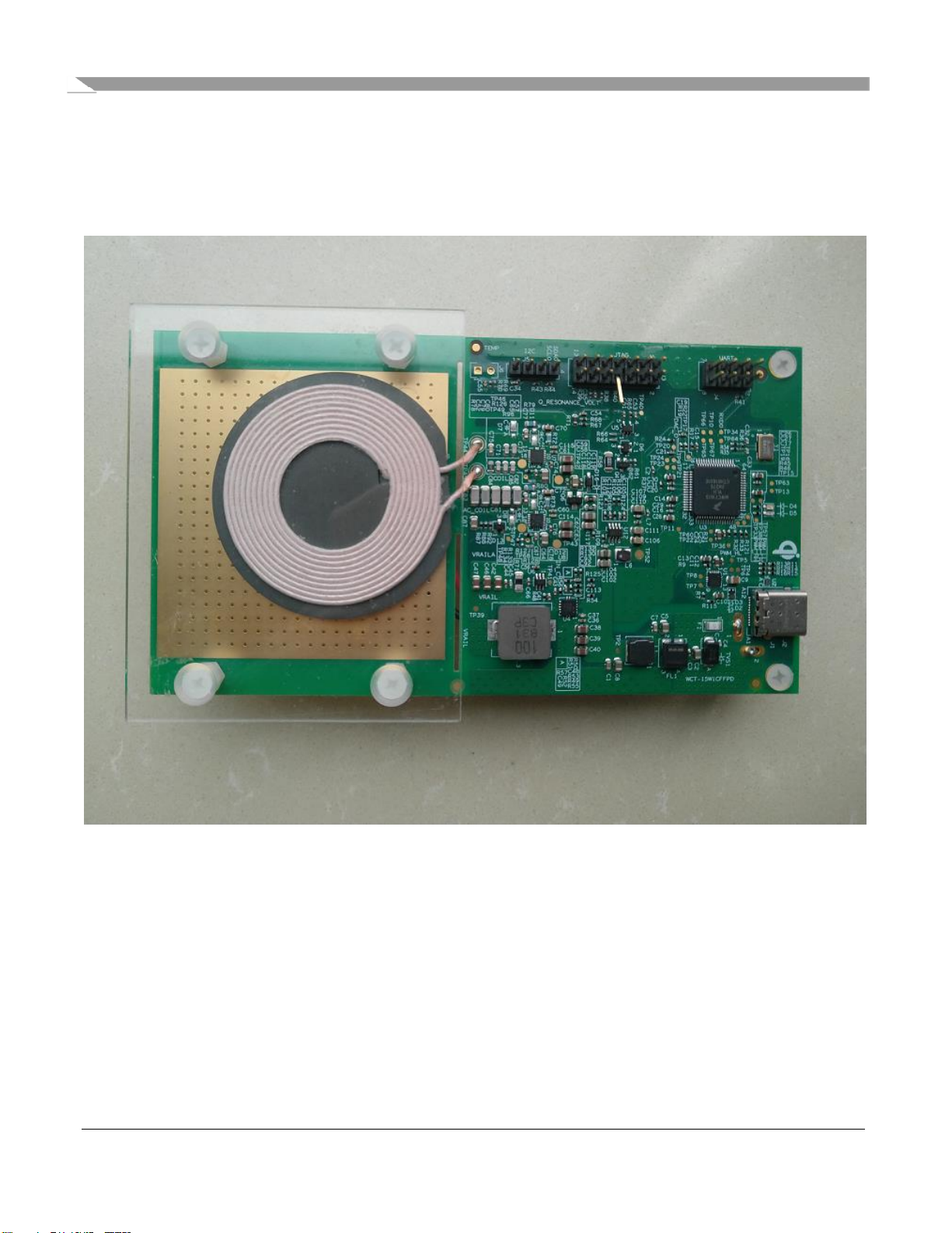
1. WCT Consumer MP-A11 (WCT-15W1CFFPD) demo board.
Figure 1. MP-A11 (WCT-15W1CFFPD) demo board
Page 3

WCT1012VLF/WCT1013VLH Consumer MP-A11 (WCT-15W1CFFPD) V1.0 Wireless Charging Application User’s
Guide, Rev. 1, 05/2019
NXP Semiconductors 3
2.2.
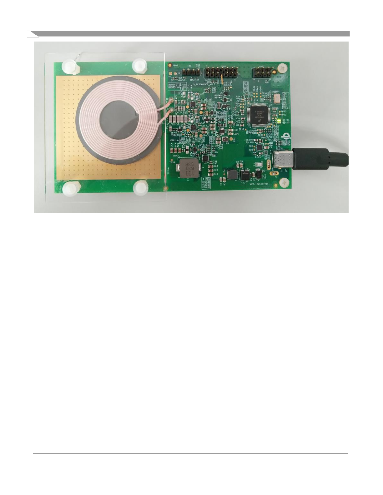
Board description
The WCT board is powered through the on-board power connector.
The connectors on the upper-middle part of the board provides the JTAG connection for programming
and debugging and 1xUART for the FreeMASTER tool connection for the debug option and console
connection. The I2C connector is placed on the upper left-hand side of the board.
Figure 2 shows the device.
Coil
I2C
UARTJTAG
DSC
USB PD
Buck
FB
Invertor
Power
Figure 2. Device overview
2.3.
Powering the board on
To power the board on, perform these steps:
1. Plug the USB PD or QC adaptor.
2. Connect the board with the USB PD or QC adaptor by an USB type-C cable.
Page 4
WCT1012VLF/WCT1013VLH Consumer MP-A11 (WCT-15W1CFFPD) V1.0 Wireless Charging Application User’s
Guide, Rev. 1, 05/2019
4 NXP Semiconductors
Figure 3. Power supply components
2.4.
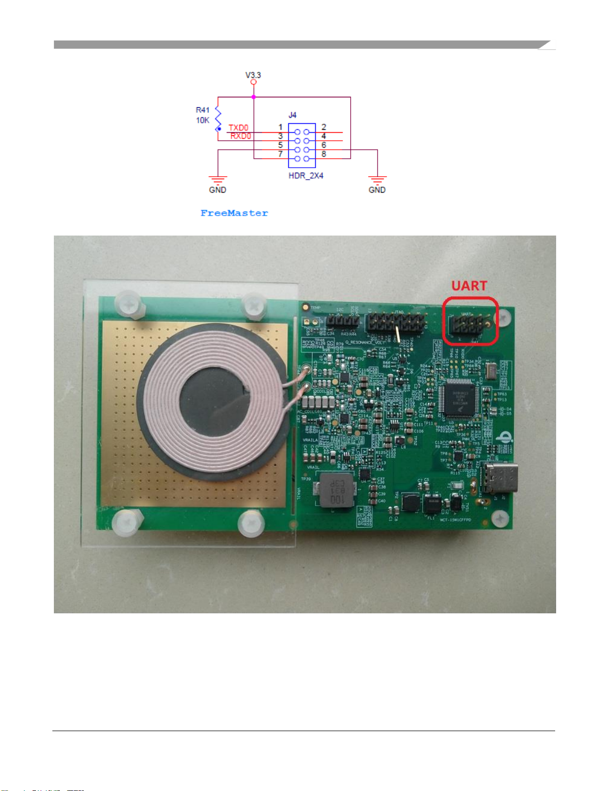
Hardware setup for FreeMASTER and console communication
To set up the hardware for the FreeMASTER and console communication, perform these steps:
1. Find the UART-to-USB adapter on the board and install the UART-to-USB device driver on the
computer. The virtual serial port on the computer should work well.
2. Plug the USB-UART converting board to the SCI connector according to the SCH signal pin
position.
Page 5
WCT1012VLF/WCT1013VLH Consumer MP-A11 (WCT-15W1CFFPD) V1.0 Wireless Charging Application User’s
Guide, Rev. 1, 05/2019
NXP Semiconductors 5
Figure 4. UART and JTAG connectors
Page 6

WCT1012VLF/WCT1013VLH Consumer MP-A11 (WCT-15W1CFFPD) V1.0 Wireless Charging Application User’s
Guide, Rev. 1, 05/2019
6 NXP Semiconductors
3. Application operation
Connect the demo to the USB PD or QC adaptor using a cable. The WCT starts to periodically send the
power ping to check whether a compatible Wireless Charging Receiver (WCR) is placed on the charging
surface.
When a Qi-compliant receiver is placed on the top of the TX coil area, the WCT starts the charging
process. If there is no correct Qi answer from the WCR side, the TX does not start the Qi charging
process.
If the WCR answers properly, the power transfer starts. The actual level of the transferred power is
controlled by the WCT in accordance with the WCR requirements. The receiver sends messages to the
WCT through the ASK on the coil resonance power signal and the transmitter sends the information to
the receiver using FSK, as per the Qi specification. The power transfer is terminated when the receiver is
removed from the WCT magnetic field.
The system supports all Qi WCR devices: Qi_Ver-1.0 compliance, Qi_Ver-1.1 compliance, and the Qi
EPP receiver. The system supports all the FOD features for different receivers. For the BPP receiver, the
power loss FOD is supported. For the EPP receiver, both the Q-value FOD method and the power loss
FOD method are supported.
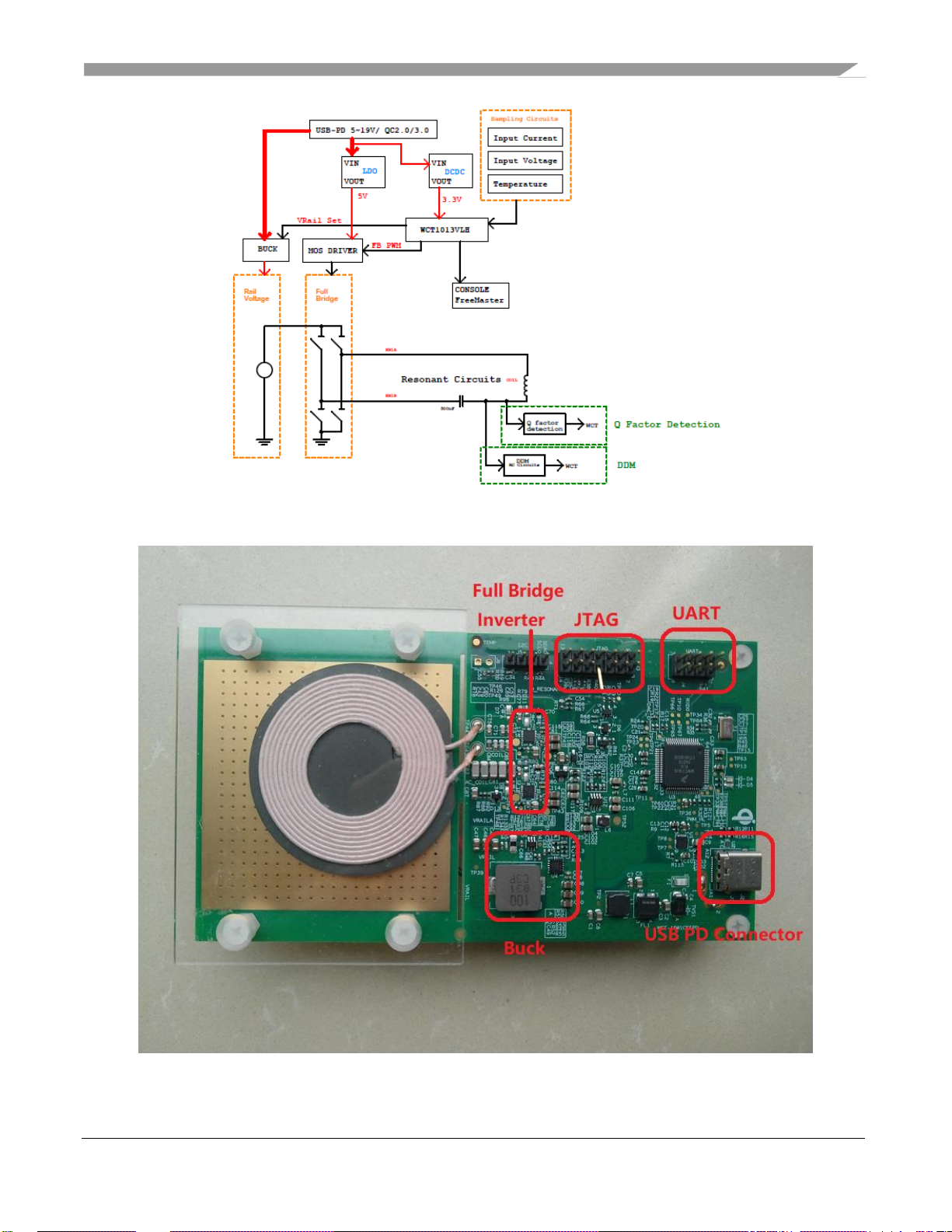
4. Hardware description
Figure 5 shows the block diagram of the consumer wireless charger MP-A11 (WCT-15W1CFFPD).
Visit www.nxp.com to get the latest hardware design files.
The whole design consists of several blocks, which are described in the following sections.
Page 7
WCT1012VLF/WCT1013VLH Consumer MP-A11 (WCT-15W1CFFPD) V1.0 Wireless Charging Application User’s
Guide, Rev. 1, 05/2019
NXP Semiconductors 7
Figure 5. Block diagram of the consumer wireless charger MP-A11 (WCT-15W1CFFPD)
Page 8
WCT1012VLF/WCT1013VLH Consumer MP-A11 (WCT-15W1CFFPD) V1.0 Wireless Charging Application User’s
Guide, Rev. 1, 05/2019
8 NXP Semiconductors
4.1.
Input EMI filter
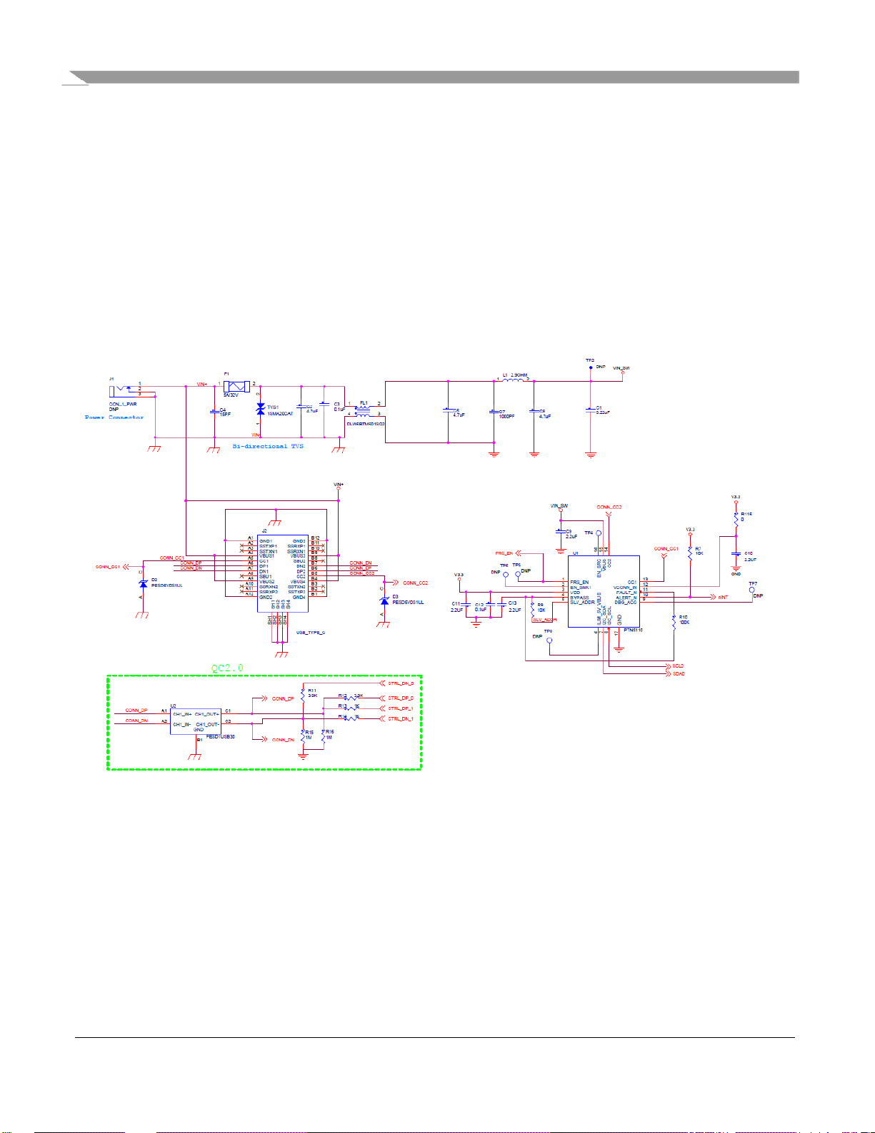
The input filter consists of the common-mode filter FL1 and filter capacitors C2, C3, C5, C7, and L1.
4.2.
USB power supply
A USB type-C cable can be plugged to the USB type-C connector J2. The PTN5110 USB PD PCTC
PHY is selected to support the type-C Configuration Channel (CC) interface and the USB PD physical
layer functions.
The MPA-11 design also supports the Qualcomm Quick Charge 2.0/3.0 technology. The WCT
controller manages the Qualcomm QC 2.0/3.0 protocol through the GPIOs and resistors connected to the
D+/D- data line.
Figure 6. USB PD power supply and QC circuits
4.3.
System voltage DCDC
The USB PD or QC adaptor input is connected to buck converter U12 (MP2314). Its output is 3.3 V.
This 3.3 V output is mainly for the WCT1012VLF/WCT1013VLH and other 3.3 V-powered
components. Generally, the DCDC load current is low. It is preferable to select a DCDC with a high
efficiency in the light-load condition.
The MP-A11 design can also support other customized-propriety power protocols.
Page 9
WCT1012VLF/WCT1013VLH Consumer MP-A11 (WCT-15W1CFFPD) V1.0 Wireless Charging Application User’s
Guide, Rev. 1, 05/2019
NXP Semiconductors 9
4.4.
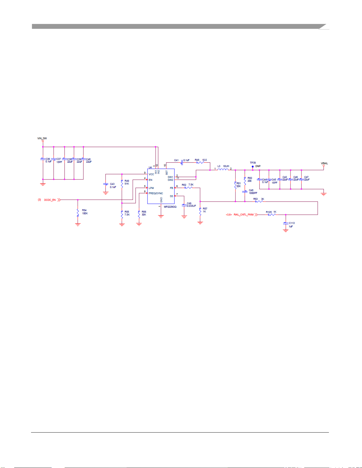
Rail voltage generated by analog buck chip
The Qi specification for the MP-A11 topology requires the DC voltage control to control the power
transferred to the receiver. The buck converter is selected to get the regulated DC voltage ranging from
3 V DC to 18 V DC for the full-bridge inverter power supply. The buck is controlled by the individual
analog buck converter and the WCT chip only controls the output voltage feedback.
For the analog buck module, MP2229 (or a similar IC like SY8286) is selected to generate the rail
voltage. The WCT chip generates one analog signal from the PWM and controls the rail voltage using
this signal. This analog signal adjusts the analog buck converter feedback, and the system can get the
rail voltage as the system expects.
Figure 7. Analog buck-boost main circuits
4.5.
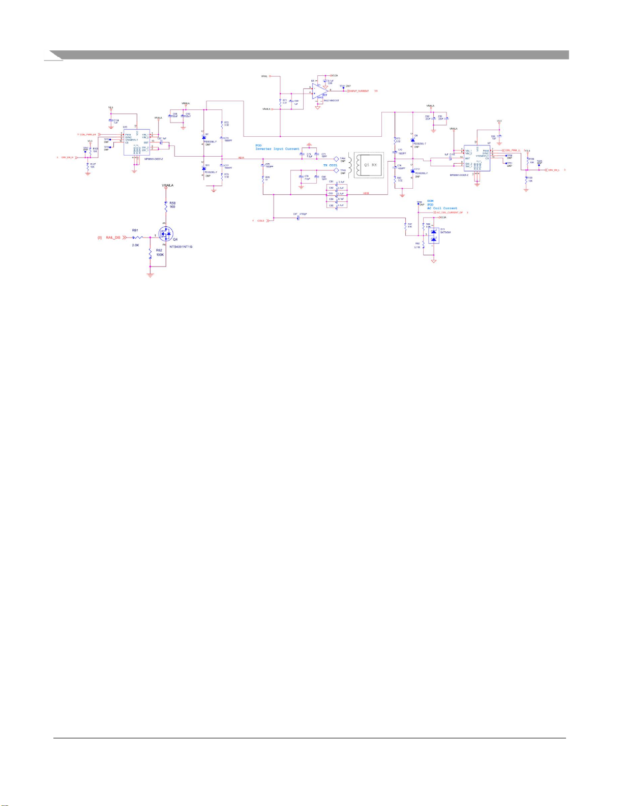
Full-bridge and resonant circuits
The full-bridge power stage consists of integrated power stage unit (U7 and U8). The MOSFETs and
their driver are integrated inside the power stage unit. The full-bridge power stage converts the variable
DC voltage VRAIL to the square-wave 50 % duty-cycle voltage with a default frequency of 127.772
kHz. The range of the frequency used (from 120 kHz to 130 kHz) is defined in the Qi specification for
the MP-A11 topology.
The resonant circuits consist of C81, C82, C83, C84, C85, and coils, all of which are fixed values
defined in the Qi specification for the MP-A11 topology. The snubber RC pairs connected in parallel to
the integrated power stages are used to lower the high frequency of the EMI products. The Vrail
discharge circuit (Q4 and R58) is switched ON while the system is terminated.
Page 10
WCT1012VLF/WCT1013VLH Consumer MP-A11 (WCT-15W1CFFPD) V1.0 Wireless Charging Application User’s
Guide, Rev. 1, 05/2019
10 NXP Semiconductors
Figure 8. Full bridge circuits
4.6.
Communication
There is bi-way communication between the EPP power transceiver and receiver. Communication from
RX to TX: The RX measures the received power and sends the information about the required power
level back to the transmitter. This message is Amplitude Modulated (AM) on the coil current and sensed
by the TX.
The RC circuits C87, R87, R88, and R92 (known as DDM) sample the signal from the coil, compress
the signal amplitude, and feed it to the ADC B-channel of the WCT1012VLF/WCT1013VLH. The
information about the current amplitude and modulated data are processed by the embedded software
routine.
Communication from TX to RX: The TX shall negotiate with the RX in the negotiation phase (if requested
by the RX). The TX uses the FSK modulation to communicate with the RX, and the communication
frequency is about 512 times the operating frequency.
4.7.
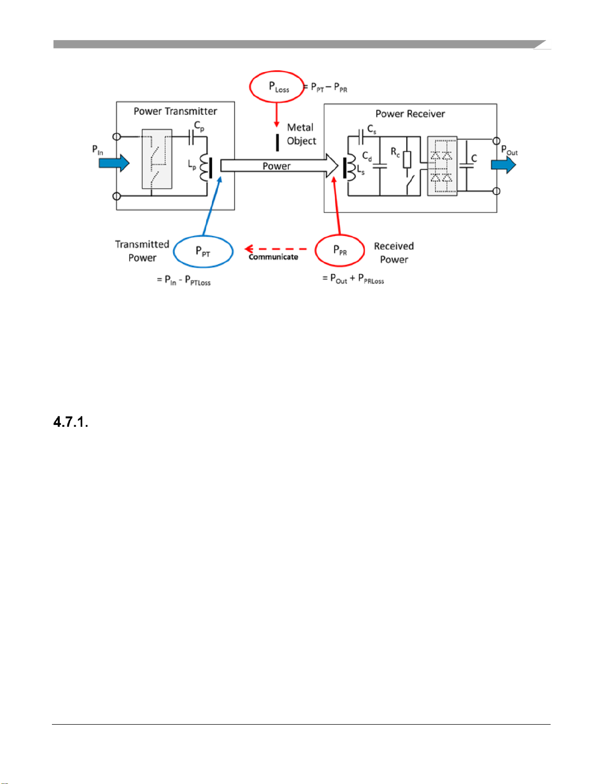
FOD based on power loss
The power loss
, which is defined as the difference between the Transmitted Power and the
Received Power , i.e.
, provides the power absorption in foreign objects, as shown
in Figure 9.
Page 11
WCT1012VLF/WCT1013VLH Consumer MP-A11 (WCT-15W1CFFPD) V1.0 Wireless Charging Application User’s
Guide, Rev. 1, 05/2019
NXP Semiconductors 11
Figure 9. Power loss illustrated
When the FO is implemented in the power transfer, the power loss increases accordingly, and the FO
can be detected based on the power loss method.
The power loss FOD method is divided into two types: FOD for the baseline power profile (TX and RX
can transfer no more than 5 W of power) and extensions power profile (TX and RX can transfer power
above 5 W).
Power-loss FOD baseline
The equation for the power-loss FOD baseline is
.
The Transmitted Power represents the amount of power that leaves the TX due to the magnetic field
of the TX, and
, where represents the input power of the TX and
is the
power dissipated inside the TX. can be measured by sampling the input voltage and input current,
and
can be estimated using the coil current.
The Received Power represents the amount of power that is dissipated within the RX due to the
magnetic field of the TX, and
. The power
is provided at the RX output and
is the power lost inside the RX.
When the NXP MP-A11 transmitter charges the baseline profile RX, the power-loss baseline is applied.
The TX continuously monitors
, and if it exceeds the threshold several times, the TX terminates
the power transfer.
Page 12

WCT1012VLF/WCT1013VLH Consumer MP-A11 (WCT-15W1CFFPD) V1.0 Wireless Charging Application User’s
Guide, Rev. 1, 05/2019
12 NXP Semiconductors
Power loss FOD extensions
Typically, the RX estimates the power loss inside itself to determine its received power. Similarly, the
TX estimates the power loss inside itself to determine its transmitted power. A systematic bias in these
estimates results in a difference between the transmitted power and the received power, even if there is
no Foreign Object (FO) present on the interface surface. To increase the effectiveness of the power-loss
method, the TX can remove the bias in the calculated power loss by calibration. For this purpose, the TX
and the power RX execute the calibration phase before the power transfer phase starts. The TX must
verify that there is no FO present on its interface surface before the calibration phase and FOD based on
the Q factor can work.
Because the bias in the estimates may depend on the power level, the TX and RX determine their
Transmitted Power and Received Power at two load conditions—a “light” load and a “connected” load.
The “light” load is close to the minimum expected output power, and the “connected” load is close to
the maximum expected output power. Based on the two load conditions, the power transmitter can
calibrate its transmitted power using linear interpolation. Alternatively, the power transmitter can
calibrate the reported received power.
Take the calibrated transmitted power as an example:
Therefore, the TX uses the calibrated transmitted power to determine the power loss as follows:
When the MP-A11 transmitter charges an RX baseline, only the power-loss FOD baseline works. If an
RX extension is placed on the MP-A11 transmitter, the Q factor is measured first to detect if there is an
FO present. If yes, the TX stops charging; otherwise, the TX can proceed to the calibration phase and
the power transfer phase, and the power-loss FOD extension works to detect if an FO is inserted during
the power transfer phase.
For more details about the FOD, see the WCT1012VLF /WCT1013VLH Consumer MP-A11 Run-Time
Debug User’s Guide (document WCT101XRTDUG).
4.8.
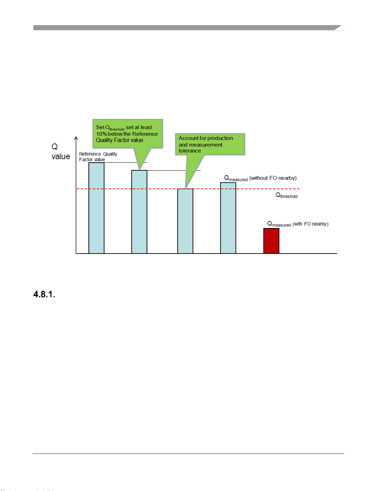
FOD based on Q factor change
A change in the environment of the TX coil typically causes its inductance to decrease or its equivalent
series resistance to increase. Both effects lead to a decrease of the TX coil’s Q factor. The RX sends a
packet including the reference Q factor for the TX to compare and determine if the FO exists, as shown
in Figure 10.
Page 13
WCT1012VLF/WCT1013VLH Consumer MP-A11 (WCT-15W1CFFPD) V1.0 Wireless Charging Application User’s
Guide, Rev. 1, 05/2019
NXP Semiconductors 13
The reference Q factor is defined as the Q factor of the test power transmitter #MP1’s primary coil at the
operating frequency of 100 kHz with RX positioned on the interface surface and no FO nearby. Due to
the differences between its design and that of the test power transmitter #MP1, the TX needs to convert
the Q factor it measured to that of the test power transmitter #MP1. NXP provides the conversion
method and must get the on-board parameters first. The TX performs the automatic calibration and gets
the parameters at the first powerup after a new image is flashed. These parameters are then written to the
flash memory. Therefore, it is necessary to ensure that there is no object on the TX surface during the
first powerup after flashing a new image.
Figure 10. Q factor threshold example
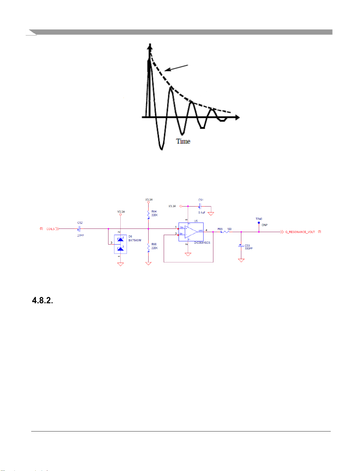
Free-resonance Q factor
The free-resonance Q factor detection detects the decay rate of the resonance signal, as shown in Figure
11. With the system’s high Q, just a few pulses near the resonant frequency are sufficient to serve as
impulses and start the system ringing. Collect the ADC data of the tank voltage (or coil current), and get
the decay rate of the signal.
Q=/(-ln(Rate))
Rate is the value of the decay rate of the resonance signal.
Page 14
WCT1012VLF/WCT1013VLH Consumer MP-A11 (WCT-15W1CFFPD) V1.0 Wireless Charging Application User’s
Guide, Rev. 1, 05/2019
14 NXP Semiconductors
Figure 11. Resonance signal
The circuit for the free-resonance Q measurement is as shown in the following figure, which samples the
signal on resonance capacitors.
Figure 12. Free-resonance Q measurement circuit
Pre-FOD based on the Q factor
The pre-FOD serves to detect foreign objects without an RX. The TX uses analog ping to detect objects.
If an object is detected, a digital ping is initiated to decide if it is an RX. If the object is a metal FO, it is
heated by a digital ping. The TX provides a pre-FOD method based on the Q factor to detect the foreign
object and prevent it from being heated before the transfer is initiated.
4.9.
Analog sensing
Some ports of the ADC A-channel of the WCT1012VLF/WCT1013VLH are used to sense analog
signals, such as the temperature, full-bridge input current, input voltage, and rail voltage.
Page 15
WCT1012VLF/WCT1013VLH Consumer MP-A11 (WCT-15W1CFFPD) V1.0 Wireless Charging Application User’s
Guide, Rev. 1, 05/2019
NXP Semiconductors 15
5. Application monitoring and control using FreeMASTER
FreeMASTER is a user-friendly real-time debug monitor and data visualization tool for application
development and information management. Supporting non-intrusive variable monitoring on a running
system, FreeMASTER allows the data from multiple variables to be viewed in an evolving
oscilloscope-like display or in a plain-text format. The application can also be monitored and operated
from the web-page-like control panel.
5.1.
Software setup
To set up the software, perform these steps:
1. Install FreeMASTER version 2.0.2 (or later) from the NXP website: www.nxp.com/freemaster.
2. Plug the USB-UART converting board to the SCI connector J4, and connect the FreeMASTER
Micro-USB port to your computer.
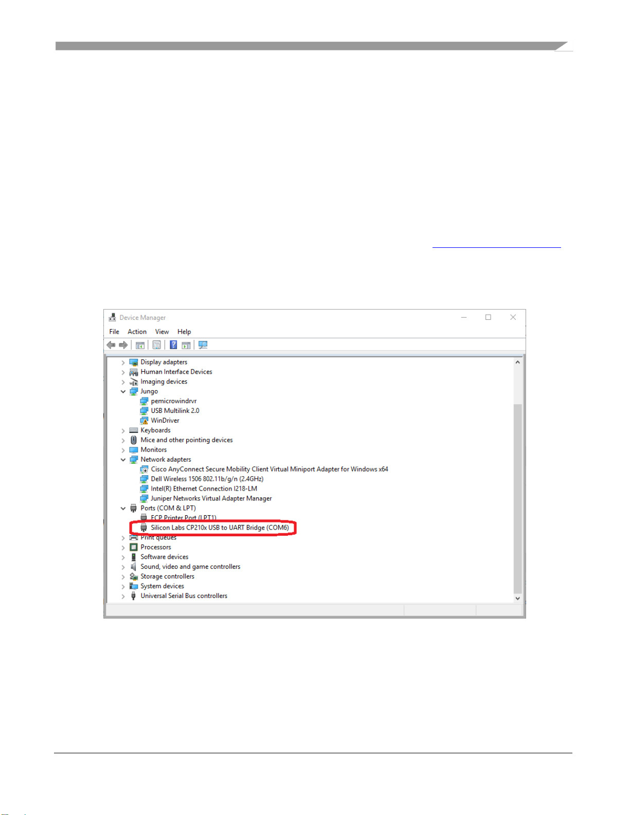
3. Open the Device Manager, and check the number of the COM port.
Figure 13. Device Manager
4. Unpack the embedded source code to your local disk.
5. Start the FreeMASTER application by opening:
• MWCT1013
<unpacked_files_location>/15W_MP/example/wct1013PD/ wct1013pd.pmp
Page 16
WCT1012VLF/WCT1013VLH Consumer MP-A11 (WCT-15W1CFFPD) V1.0 Wireless Charging Application User’s
Guide, Rev. 1, 05/2019
16 NXP Semiconductors
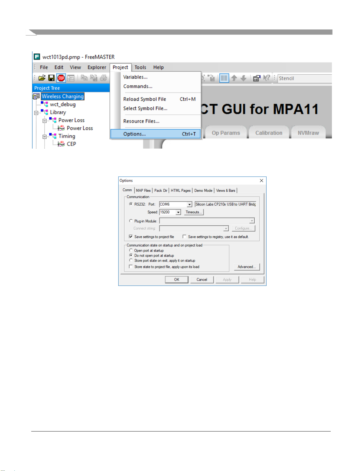
6. Choose “Project” –> “Options”.
Figure 14. Choosing “Options”
7. Ensure that the correct virtual port (according to Step 3) and speed are selected.
Figure 15. Setting port and speed
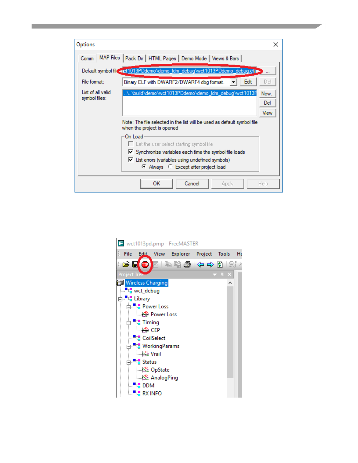
8. Ensure that the MAP file is correct. The default directories are:
• MWCT1013
<unpacked_files_location>/15W_MP/build/demo/wct1013PDdemo/demo_ldm_debug/wct1013P
Ddemo_debug.elf
Page 17
WCT1012VLF/WCT1013VLH Consumer MP-A11 (WCT-15W1CFFPD) V1.0 Wireless Charging Application User’s
Guide, Rev. 1, 05/2019
NXP Semiconductors 17
Figure 16. Setting the MAP file
9. Connect FreeMASTER.
Power the MP-A11 on and start the communication by clicking the “STOP” button in the
FreeMASTER GUI.
Figure 17. “STOP” button
Page 18
WCT1012VLF/WCT1013VLH Consumer MP-A11 (WCT-15W1CFFPD) V1.0 Wireless Charging Application User’s
Guide, Rev. 1, 05/2019
18 NXP Semiconductors
5.2.
Real-time application variables monitoring
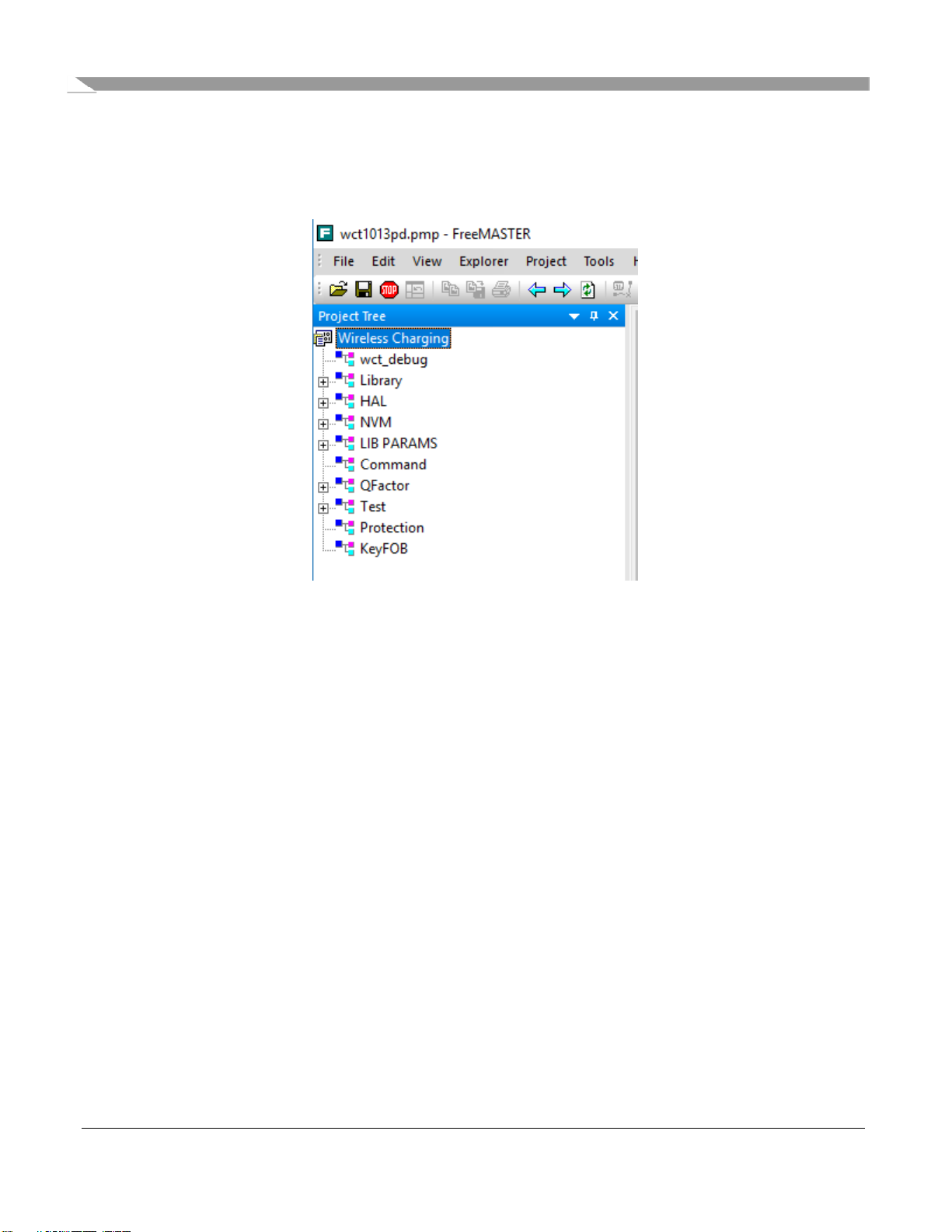
FreeMASTER enables the monitoring and updating of all the application global variables. In this
application, several key variables are displayed in the scope windows. These variables are divided into
different blocks, as shown in the following figure.
Figure 18. Real-time application variables
• wct_debug
This block shows the variables used for the GUI command.
• Library
This block contains the power loss variables, timing variables, coil selection variables, working
parameters, system status, DDM variables, and RX information.
• HAL
This block contains the ADC raw data and DDM buffer values.
• NVM
This block lists all NVM parameters. The Q factor sub-block shows the Q factor calibration
constants. The RRQD sub-block shows the quick-removal calibration constants. The FOD
sub-block shows the FOD characterization calibration constants. The normalization sub-block
shows the FOD normalization constants. The analog sub-block shows the rail voltage calibration
constants.
• LIB PARAMS
This block lists all the parameters used for the WCT library.
• Command
The command variable is used to stop the WCT, start the WCT, and perform automatic
calibration.
Page 19

WCT1012VLF/WCT1013VLH Consumer MP-A11 (WCT-15W1CFFPD) V1.0 Wireless Charging Application User’s
Guide, Rev. 1, 05/2019
NXP Semiconductors 19
• QFactor
This block contains the variables for the Q factor detection.
• Test
This block contains some variables for debugging.
• Protection
This block contains protection variables, such as the input voltage protection, input current
protection, and temperature protection.
NOTE
Besides the above variables, all the global variables can be added to
FreeMASTER. The procedure to generate and add variables to the watch
window is described in the FreeMASTER user manual.
5.3.
Application parameters modification
The application parameters (NVM parameters) can be easily viewed and changed in the control panel.
The control panel contains the web page elements (buttons, check boxes, and text fields) that enable a
user-friendly way to visualize and change the application control parameters.
Figure 19. Application variables
The application variables are divided into these tabs:
• “Op Params”—enables access to variables related to the operation control.
Page 20

WCT1012VLF/WCT1013VLH Consumer MP-A11 (WCT-15W1CFFPD) V1.0 Wireless Charging Application User’s
Guide, Rev. 1, 05/2019
20 NXP Semiconductors
• “Calibration”—a group of parameters for calibration of the input current, input voltage, and
foreign objects detector.
The meaning of each parameter is described next to the text field.
NOTE
The parameters of the “Calibration” tab can be changed at
run-time, but the parameters of the “Op Params” tab cannot take
effect immediately. To modify the parameters in the “Op Params”
page: enter the debug mode, modify the parameters, and exit the
debug mode. The parameters can then take effect.
6. Application monitoring using console
The application sends some information and error states through the SCI to the console. The information
is sent when the board is turned on, when the device is charging, or in case of an error state.
On the MP-A11 design, only one SCI port (SCI0) is available on the J4 connector. SCI0 is used for
FreeMASTER by default. Select an alternative method to enable the debug console.
1. Disable FreeMASTER and configure the SCI0 as the debug console.
a) #define DEBUG_CONSOLE_SUPPORTED (TRUE)
#define FREEMASTER_SUPPORTED (FASLE)
The macros are defined in example->wct101xa–>configure-> appcfg.h.
b) #define QSCI_CONSOLE_INDEX 0
#define QSCI_FREEMASTER_INDEX 1
The macros are defined in example->wct101xa->driver->qsci.h.
c) gWCT_Params.tDebugConfig.bGeneralDbg = 1;
This variable is in wct_LibParams.c.
2. Change the FreeMASTER communication interface to JTAG and configure the SCI0 as the debug
console.
a) #define DEBUG_CONSOLE_SUPPORTED (TRUE)
#define FREEMASTER_SUPPORTED (TRUE)
The macros are defined in example->wct101xa–>configure-> appcfg.h.
b) #define QSCI_CONSOLE_INDEX 0
#define QSCI_FREEMASTER_INDEX 1
The macros are defined in example->wct101xa->driver->qsci.h.
c) #define FMSTR_USE_SCI 0 /* To select SCI communication interface */
#define FMSTR_USE_JTAG 1 /* 56F8xxx: use JTAG interface */
Page 21

WCT1012VLF/WCT1013VLH Consumer MP-A11 (WCT-15W1CFFPD) V1.0 Wireless Charging Application User’s
Guide, Rev. 1, 05/2019
NXP Semiconductors 21
The macros are defined in example->wct101xa–>configure-> freemaster_cfg.h.
d) gWCT_Params.tDebugConfig.bGeneralDbg = 1;
This variable is in wct_LibParams.c.
6.1.
Software setup
1. Plug the USB-UART converting board to SCI connector J4 and connect the console Micro-USB
port to the computer.
2. Open the Device Manager and check the number of the COM port.
Figure 20. Device Manager
3. Run the communication program supporting console, such as HyperTerminal or RealTerm.
4. The following table shows the communication setup.
Table 1. Port configurations
Port number
Serial port from Device Manager
Baud
19200
Data Bits
8
Stop Bits
1
Parity
None
Hardware Flow Control
None
Display As
ASCII
5. Open the port or start the communication, depending on the terminal used.
Page 22

WCT1012VLF/WCT1013VLH Consumer MP-A11 (WCT-15W1CFFPD) V1.0 Wireless Charging Application User’s
Guide, Rev. 1, 05/2019
22 NXP Semiconductors
7. Programming new software and calibration
The provided software package includes a WCT1013 project and a binary file (.elf or .S). You can flash
the alternative to the board. After flashing a new software, carry out the board calibration.
7.1.
Installing the latest CodeWarrior IDE
NOTE
The following steps demonstrate the installation of the CodeWarrior for
Microcontrollers v10.7 IDE as an example. You can also select a later
version.
1. Download installation files.
For a proper installation of CodeWarrior 10.7, install both the CodeWarrior for Microcontrollers
10.7 IDE and the CodeWarrior for MCUs v10.7 service pack.
Access the following webpage and log in:
www.nxp.com/products/developer-resources/software-development-tools/codewarriordevelopment-tools/codewarrior-development-suites/codewarrior-development-suite-special:CWSUITE-SPECIAL?tab=Design_Tools_Tab
Click the “Download” button for the CodeWarrior Special Edition (offline or online).
Figure 21. Clicking “Download” for CodeWarrior Special Edition
Download the CodeWarrior for Microcontrollers 10.7 service pack at this link:
www.nxp.com/products/power-management/wireless-charging-ics/15-watt-wireless-chargingtransmitter-ics-for-automotive-applications:MWCT1x1xA?tab=Design_Tools_Tab
Page 23

WCT1012VLF/WCT1013VLH Consumer MP-A11 (WCT-15W1CFFPD) V1.0 Wireless Charging Application User’s
Guide, Rev. 1, 05/2019
NXP Semiconductors 23
Figure 22. Downloading CodeWarrior for MCU v10.7 service pack
2. Double-click the CW_MCU_v10.7_b160721_SE.exe file after downloading.
Figure 23. Setup file
3. Make sure that the “DSC” option is selected.
Figure 24. DSC installed
Page 24

WCT1012VLF/WCT1013VLH Consumer MP-A11 (WCT-15W1CFFPD) V1.0 Wireless Charging Application User’s
Guide, Rev. 1, 05/2019
24 NXP Semiconductors
4. Launch CodeWarrior, create a folder workspace, and select it as the default workspace.
Figure 25. Workspace Launcher dialog box
5. Select “Help” –> “Install New Software”.
Figure 26. Install New Software
Page 25

WCT1012VLF/WCT1013VLH Consumer MP-A11 (WCT-15W1CFFPD) V1.0 Wireless Charging Application User’s
Guide, Rev. 1, 05/2019
NXP Semiconductors 25
6. Click the “Add”, “Archive”, and then select the
mcu10_7.Wireless_Charging_MWCT101x.win.sp.v1.0.1.zip file.
Figure 27. Selecting the update pack
7. Select the “MCU v10.7 DSC Service Packs” option, and then click “Next”.
Figure 28. Selecting service packs
8. Review the license terms. If you agree with the license terms, select “I accept the terms of the
license agreement” and then click “Finish”.
Page 26

WCT1012VLF/WCT1013VLH Consumer MP-A11 (WCT-15W1CFFPD) V1.0 Wireless Charging Application User’s
Guide, Rev. 1, 05/2019
26 NXP Semiconductors
Figure 29. Installation finished
7.2.
Board and programmer connection
Connect the 14-pin debug cable to J3 on the board (notice the pin-1 position of the cable).
Page 27

WCT1012VLF/WCT1013VLH Consumer MP-A11 (WCT-15W1CFFPD) V1.0 Wireless Charging Application User’s
Guide, Rev. 1, 05/2019
NXP Semiconductors 27
Figure 30. Connecting the debug cable to the board
7.3.
Programming project files
1. Import a project.
2. Select the “File” tab and then click the “Import” button to import an existing project, as shown in
the following figures.
Page 28

WCT1012VLF/WCT1013VLH Consumer MP-A11 (WCT-15W1CFFPD) V1.0 Wireless Charging Application User’s
Guide, Rev. 1, 05/2019
28 NXP Semiconductors
Figure 31. Importing a project (1)
Figure 32. Importing a project (2)
Page 29

WCT1012VLF/WCT1013VLH Consumer MP-A11 (WCT-15W1CFFPD) V1.0 Wireless Charging Application User’s
Guide, Rev. 1, 05/2019
NXP Semiconductors 29
3. Select the project directory, as shown in the following figure.
Figure 33. Importing a project (3)
4. Select the WCT1013 project.
Page 30

WCT1012VLF/WCT1013VLH Consumer MP-A11 (WCT-15W1CFFPD) V1.0 Wireless Charging Application User’s
Guide, Rev. 1, 05/2019
30 NXP Semiconductors
Figure 34. Importing a project (4)
5. Build a project.
Select the build configurations by clicking the project name in the project window, as shown in
the following figure. The “demo_ldm_debug” build contains debug information. The
“demo_ldm_release” is the same as the “demo_ldm_debug”, except for debug information.
Figure 35. Building a project (1)
Page 31

WCT1012VLF/WCT1013VLH Consumer MP-A11 (WCT-15W1CFFPD) V1.0 Wireless Charging Application User’s
Guide, Rev. 1, 05/2019
NXP Semiconductors 31
6. Right-click “wct1013demo” and select the “Clean Project” and “Build Project” options.
Figure 36. Clean Project and Build Project options
7. Download the project.
Download the project from the “Debug” drop-down list or from “Run” -> “Debug”. In
“Download Configurations”, select a download configuration according to your build
configurations and debugger type: USB TAP, PnE Multilink, or OSJTAG.
Figure 37. Downloading the project
Page 32

WCT1012VLF/WCT1013VLH Consumer MP-A11 (WCT-15W1CFFPD) V1.0 Wireless Charging Application User’s
Guide, Rev. 1, 05/2019
32 NXP Semiconductors
After the project is downloaded, the MCU stops at the startup code. Click the “Run” button or
press the “F8” key to run the MCU. Make sure that there is no object on the TX surface before
running the MCU. Due to the automatic calibration of the rail voltage, the Q-factor and quick
removal is done the first time the TX runs after flashing a new image.
Figure 38. Project downloaded
Page 33

WCT1012VLF/WCT1013VLH Consumer MP-A11 (WCT-15W1CFFPD) V1.0 Wireless Charging Application User’s
Guide, Rev. 1, 05/2019
NXP Semiconductors 33
7.4.
Programming the binary file (.elf or .S)
1. Select “Flash Programmer” –> “Flash File to Target”.
Figure 39. Choosing Flash File to Target
2. Click the “New” button to create a new connection.
Page 34

WCT1012VLF/WCT1013VLH Consumer MP-A11 (WCT-15W1CFFPD) V1.0 Wireless Charging Application User’s
Guide, Rev. 1, 05/2019
34 NXP Semiconductors
Figure 40. Creating a new connection
3. In the “New Connection” text box, select “Hardware or Simulator Connection” and click “Next”.
Figure 41. Entering a connection name
Page 35

WCT1012VLF/WCT1013VLH Consumer MP-A11 (WCT-15W1CFFPD) V1.0 Wireless Charging Application User’s
Guide, Rev. 1, 05/2019
NXP Semiconductors 35
4. In the “Name” text box, enter a connection name (any name is OK), and click “New” to create a
target.
Figure 42. Entering a connection name
5. In the “Name” text box, enter a target name (any name is OK, but it cannot be the same as the
connection name) and choose “dsc.MWCT101x” -> “MWCT1013A” from the “Target Type”
drop-down menu.
Page 36

WCT1012VLF/WCT1013VLH Consumer MP-A11 (WCT-15W1CFFPD) V1.0 Wireless Charging Application User’s
Guide, Rev. 1, 05/2019
36 NXP Semiconductors
Figure 43. Choosing MWCT1013A
6. Select “Execute reset” and “Initialize target”, set the initialization target file path to the
CodeWarrior IDE installation folder, and then select MWCT1013A.tcl.
Page 37

WCT1012VLF/WCT1013VLH Consumer MP-A11 (WCT-15W1CFFPD) V1.0 Wireless Charging Application User’s
Guide, Rev. 1, 05/2019
NXP Semiconductors 37
Figure 44. Executing reset and initializing target
7. Click the “Memory” tab.
8. Select “Memory configuration”, set the memory configuration file path to the CodeWarrior IDE
installation folder, and then select “MWCT1013A.mem”.
9. Click “Finish”.
Page 38

WCT1012VLF/WCT1013VLH Consumer MP-A11 (WCT-15W1CFFPD) V1.0 Wireless Charging Application User’s
Guide, Rev. 1, 05/2019
38 NXP Semiconductors
Figure 45. Memory configuration
10. Select “USB TAP” for the “Connection type”, and then click “Finish”.
Page 39

WCT1012VLF/WCT1013VLH Consumer MP-A11 (WCT-15W1CFFPD) V1.0 Wireless Charging Application User’s
Guide, Rev. 1, 05/2019
NXP Semiconductors 39
Figure 46. Setting the connection type
11. Set the binary file path to “File to Flash”. Select “Save the Target Task” for future programming.
Power the MP-A11 on and click “Erase and Program”.
Page 40

WCT1012VLF/WCT1013VLH Consumer MP-A11 (WCT-15W1CFFPD) V1.0 Wireless Charging Application User’s
Guide, Rev. 1, 05/2019
40 NXP Semiconductors
Figure 47. Erase and Program
12. Specify the task path and click “OK” to save the task.
Figure 48. Selecting the task path
13. When program is finished, the “Console” window displays the following log.
Figure 49. Programming finished log
Page 41

WCT1012VLF/WCT1013VLH Consumer MP-A11 (WCT-15W1CFFPD) V1.0 Wireless Charging Application User’s
Guide, Rev. 1, 05/2019
NXP Semiconductors 41
7.5.
Programming by bootloader
The bootloader is independent of the application codes and can reside in the flash forever after the
application code is downloaded. When a system is reset, the bootloader starts. After a boot delay (in
seconds), the bootloader jumps to the programmed application code without receiving the application
S-record file. When receiving the application S-record file, the bootloader programs the application code
to the on-chip flash. After completion, the bootloader jumps to the application startup code.
1. The bootloader code is not flashed to the board by default. Download the bootloader code.
Import the bootloader project and follow the steps described in Section 7.3 to download the
project.
Figure 50. Bootloader project
2. Generate an application S-record file.
Enable the bootloader function. Set the following macro to TRUE in appcfg.h.
#define BOOTLOADER_USED (TRUE)
See the figure below to configure the application project settings. Select the “Sort by Address”
option. Set “Max S-Record Length” to a value that does not exceed 255. Select “DOS (\\r\\n)”
for the “S-Record EOL Character”.
Page 42

WCT1012VLF/WCT1013VLH Consumer MP-A11 (WCT-15W1CFFPD) V1.0 Wireless Charging Application User’s
Guide, Rev. 1, 05/2019
42 NXP Semiconductors
Figure 51. Configure project settings
Recompile the project after completing the configuration above. The generated S-record file is in
the <unpacked_files>\15W_MP\build\demo\wct1013PDdemo\demo_ldm_debug folder for the
WCT1013 chip. The S-record file is the combined p and x S-record file without “.p” or “.x” in
the extension name (.s).
3. Download the application code using the bootloader.
Most serial terminal programs can be used to send the S-Record file from the host to the
WCT1013 board using the bootloader. For example, Tera Term can be used in the Windows OS
platform.
Page 43

WCT1012VLF/WCT1013VLH Consumer MP-A11 (WCT-15W1CFFPD) V1.0 Wireless Charging Application User’s
Guide, Rev. 1, 05/2019
NXP Semiconductors 43
SCI0 is used for communication. Plug the USB-UART converter to the SCI connector J2 and the
computer. Open Tera Term, and select “Serial” and “Port”. Check the COM port in the Device
Manager.
Figure 52. Tera Term connection
4. Choose “Setup” -> “Serial port” to configure the COM properties, as shown in the following
figure.
Figure 53. Serial port
Page 44

WCT1012VLF/WCT1013VLH Consumer MP-A11 (WCT-15W1CFFPD) V1.0 Wireless Charging Application User’s
Guide, Rev. 1, 05/2019
44 NXP Semiconductors
Figure 54. Serial port setup
5. Choose “File” -> “Send file”.
Figure 55. Send file
6. Select the application S-Record file and click “Open”.
Page 45

WCT1012VLF/WCT1013VLH Consumer MP-A11 (WCT-15W1CFFPD) V1.0 Wireless Charging Application User’s
Guide, Rev. 1, 05/2019
NXP Semiconductors 45
Figure 56. Send application S-Record file
The download progress is displayed in the Tera Term window. After the download completes,
the application code starts.
Figure 57. S-Record file download complete
Page 46

WCT1012VLF/WCT1013VLH Consumer MP-A11 (WCT-15W1CFFPD) V1.0 Wireless Charging Application User’s
Guide, Rev. 1, 05/2019
46 NXP Semiconductors
7.6.
Board calibration
NXP provides the FreeMASTER GUI tool for calibration and parameters tuning. For board calibration,
see the WCT1012VLF/WCT1013VLH Consumer MP-A11 V1.0 Run-Time Debugging User’s Guide
(document WCT101XV10RTDUG).
8. Software description
8.1.
Software overview
Directory structure
The following figure shows an example of the directory structure of the whole WCT1013_MP-A11
distribution.
Figure 58. Directory structure of the whole WCT1013_MP-A11 distribution
Page 47

WCT1012VLF/WCT1013VLH Consumer MP-A11 (WCT-15W1CFFPD) V1.0 Wireless Charging Application User’s
Guide, Rev. 1, 05/2019
NXP Semiconductors 47
8.2.
CodeWarrior projects
There are four CodeWarrior projects in the package. The following figure shows all four projects in the
CodeWarrior GUI when all of them are imported.
Figure 59. CodeWarrior projects
Combined with different program models and different user cases, multiple build configurations are
predefined in the respective projects.
There are two program models provided for the WCT parts.
• Small program model: The compiler generates a more efficient switch table when the code is in
the range of 0x0-0xFFFF. This model is more efficient, but the code size is limited to 64-KB
words.
• Larger program model: Extends the DSP56800E addressing range by providing 24-bit address
capability to the instructions. This enables the user accesses beyond the 64-KB word boundary of
16-bit addressing.
For the WCT1013 of the MP-A11 design, only the larger program model is provided.
For WCT1013, there are two build configurations:
• “demo_ldm_debug”: larger program model, including the code for debugging.
• “demo_ldm_release”: larger program model, excluding the debugging code to save memory size.
Page 48

WCT1012VLF/WCT1013VLH Consumer MP-A11 (WCT-15W1CFFPD) V1.0 Wireless Charging Application User’s
Guide, Rev. 1, 05/2019
48 NXP Semiconductors
Figure 60. WCT1013 build configuration
8.3.
Functional description
NXP provides full-featured wireless charging functions on the reference board. If a certain function is
not needed, disable it by the definitions in the header file.
FreeMASTER
• FreeMASTER is supported. The following configuration is used to enable or disable it.
Table 2. FreeMASTER configurations
Configurations
Default value
Location
Description
FREEMASTER_SUPPORTED
TRUE
appcfg.h
Enables or disables the function. Set
TRUE to enable it. Set FALSE to
disable it.
• FreeMASTER communication interface configuration is in freemaster_cfg.h. The SCI
interface is enabled and the JTAG interface is disabled by default. Only one interface can be
set at a time.
#define FMSTR_USE_SCI 1 /* To select SCI communication interface */
#define FMSTR_USE_JTAG 0 /* 56F8xxx: use JTAG interface */
• The FreeMASTER SCI port is SCI0 by default.
1) #define FMSTR_SCI_BASE 0xE080 /* base address of SCI_0 */
The macro is in freemaster_cfg.h.
2) #define QSCI_FREEMASTER_INDEX 0 //QSCI0
The macro is in qsci.h.
Page 49

WCT1012VLF/WCT1013VLH Consumer MP-A11 (WCT-15W1CFFPD) V1.0 Wireless Charging Application User’s
Guide, Rev. 1, 05/2019
NXP Semiconductors 49
Low-power mode
The low-power mode is supported. In the analog ping interval, the MCU enters the LPSTOP mode and
the DCDC module is closed. The following configuration is used to enable or disable it.
Table 3. Low power mode configurations
Configurations
Default value
Location
Description
LOW_POWER_MODE_ENABLE
FALSE
appcfg.h
Enables or disables the function.
Set TRUE to enable it. Set
FALSE to disable it.
Debug console
The debug console is supported. The following configuration is used to enable or disable it.
Table 4. Debug console configurations
Configurations
Default value
Location
Description
DEBUG_CONSOLE_SUPPORTED
FALSE
appcfg.h
Enables or disables the
function. Set TRUE to enable it.
Set FALSE to disable it.
For the WCT1011A/WCT1013A digital buck-boost platform, only one SCI port is available. This port is
used for FreeMASTER by default. If the debug console is used, disable the FreeMASTER or change the
FreeMASTER communication interface to JTAG. The configurations are described in Chapter 6.
Bootloader
Bootloader is supported. The following configuration is used to enable or disable it.
Table 5. Bootloader configurations
Configurations
Default value
Location
Description
BOOTLOADER_USED
FALSE
appcfg.h
Enables or disables the function. Set
TRUE to enable it. Set FALSE to
disable it.
If the bootloader is used, download the bootloader project to the board. Then change
BOOTLOADER_USED to TRUE, rebuild the application project, and download the application .s file
using the bootloader.
DCDC control type
NXP provides two DCDC control types: digital buck-boost and analog buck-boost. Because the MPA11
design doesn’t use the buck-boost circuit, the default one shall be FALSE.
Table 6. DCDC control type configurations
Configurations
Default value
Location
Description
DIGITAL_BUCKBOOST
FALSE
appcfg.h
Switch the DCDC control type. Set
TRUE to enable the digital
buck-boost. Set FALSE to enable the
analog buck-boost.
Page 50

WCT1012VLF/WCT1013VLH Consumer MP-A11 (WCT-15W1CFFPD) V1.0 Wireless Charging Application User’s
Guide, Rev. 1, 05/2019
50 NXP Semiconductors
Library functions
Some key functions are implemented in the WPC library and can be enabled or disabled in the
application. The following configurations are used to enable or disable them.
Table 7. Library functions configurations
Function
Function description
Variables
Default
value
Description
FOD
Foreign object detection
based on power loss
during power transfer
state
gWCT_Params.uCtrlBit.bFODEnable
1
FOD feature enable
or disable. 1:
enable, 0: disable.
RX removal
quick
detection
RX removal quick
detection based on
current and voltage (~350
ms) instead of
communication timeout
(1.5 s)
gWCT_Params.uCtrlBit.bRRQDEnable
1
RX removal quick
detection enable or
disable. 1: enable, 0:
disable.
Safe digital
ping
Digital ping with lower
coupling to avoid large
current damage of a large
metal
gWCT_Params.uCtrlBit.bSafeDPEnabl
e
1
Safe digital ping
enable or disable. 1:
enable, 0: disable.
Maximum
voltage limit
Refer to MVL in the WPC
Qi specification
gWCT_Params.uCtrlBit.bMVLEnable
1
Maximum voltage
limit enable or
disable. 1: enable, 0:
disable.
Fast charging
Enable fast charging for
some types of phones,
contact NXP for details
gWCT_Params.uCtrlBit.bFastCharging
Enable
1
Fast charging
enable or disable. 1:
enable, 0: disable.
Analog ping
Use several power pulses
to detect object before
digital ping
gWCT_Params.uCtrlBit.bAnalogPingDi
sable
0
Analog ping enable
or disable. 0:
enable, 1: disable.
Q factor
recharge retry
Foreign object removal
detection based on Q
factor method during
recharge retry state
gWCT_Params.uCtrlBit.bQfactorRetry
1
Using Q factor
method for recharge
retry state. 1:
enable, 0: disable.
Maximum
power limit
TX maximum output
power limit
gWCT_Params.uCtrlBit.bMPLEnable
1
Maximum power
limit enable or
disable. 1: enable, 0:
disable.
Active power
protection
Refer to overvoltage
protection in the WPC Qi
specification
gWCT_Params.uCtrlBit.bActivePower
ProtectionEnable
1
Active power
protection enable or
disable. 1: enable, 0:
disable
Low-power
mode for
recharge retry
state
Low-power mode enable
or disable when TX is
under the recharge retry
state
gWCT_Params.uCtrlBit.bRechargeRet
ryLowPowerEnable
0
Low power mode
enable or disable
under recharge retry
state. 1: enable, 0:
disable
Page 51

WCT1012VLF/WCT1013VLH Consumer MP-A11 (WCT-15W1CFFPD) V1.0 Wireless Charging Application User’s
Guide, Rev. 1, 05/2019
NXP Semiconductors 51
Power down
for maximum
rail voltage
Power down or keep the
maximum rail voltage
when rail voltage exceeds
the maximum
gWCT_Params.uCtrlBit.bPowerDownF
orMaxVrail
1
Power down or not
when rail voltage
exceed maximum
value. 1: power
down,
0: keep maximum
“Not Res
Sens” bit for
TX capability
packet
Set “Not Res Sens” bit for
TX capability packet
gWCT_Params.uCtrlBit.bNotResSens
1
Set the value of Not
Res Sens bit for TX
capability packet, 0:
set this bit to 0, 1:
set this bit to 1
Pre-FOD
FOD protection when TX
is in standby state
gWCT_Params.uCtrlBit.bPreFODEnab
le
1
Pre-FOD enable or
disable during
standby state,
1:enable, 0:disable
Duty cycle
control
Duty cycle control when
TX rail voltage is down to
minimum value
gWCT_Params.uCtrlBit.bEnableDutyC
ycleControlForMinRailVol
0
Duty cycle control
enable or disable,
1:enable, 0:disable
BPP
transmitter
TX behaves as BPP
transmitter
gWCT_Params.uCtrlBit.bBPPOnly
0
Only BPP mode
enable or disable. 1:
BPP mode, 0: EPP
mode
8.4.
Protection mechanisms
The following table lists the protection that can be implemented.
Table 8. Protection mechanisms
Protection
Default limits
Variables
Description
Rail voltage
17000 mV
gPROT_Params.wMaxRailVol
Application implemented. If the rail voltage
exceeds the limit, charging is turned off. The
limit value can be changed by
FreesMASTER GUI.
Battery voltage
Min: 8000 mV
Max: 22000
mV
Hysteresis:
1000 mV
gPROT_Params.wMinBatteryVol
gPROT_Params.wMaxBatteryVol
gPROT_Params.wBatteryHystVol
Application implemented. If the battery
voltage exceeds the maximum, the WCT
library stops. When the battery voltage is
lower than the difference between the
maximum and hysteresis, the WCT library
starts. When the battery voltage is lower
than the minimum, the WCT library stops.
When the battery voltage is higher than the
sum of the minimum and hysteresis, the
WCT library starts.
The minimum and maximum limits can be
changed by the FreeMASTER GUI. The
hysteresis value can be changed in
PROT_Init().
Input current
5000 mA
gPROT_Params.wMaxInputCurrent
Application implemented. If the input current
exceeds the limit, charging is turned off. The
limit value can be changed by the
FreeMASTER GUI.
Page 52

WCT1012VLF/WCT1013VLH Consumer MP-A11 (WCT-15W1CFFPD) V1.0 Wireless Charging Application User’s
Guide, Rev. 1, 05/2019
52 NXP Semiconductors
Coil current
8000 mA
gPROT_Params.wMaxCoilCurrent
Application implemented. If the coil current
exceeds the limit, charging is turned off. The
limit value can be changed by the
FreeMASTER GUI.
Temperature
Max: 60
Hysteresis:
10
gPROT_Params.swTemperatureThres
hold
gPROT_Params.wTemperatureHyst
Application implemented. If the temperature
exceeds the maximum, the WCT library
stops. When the temperature is lower than
the difference between the maximum and
hysteresis, the WCT library starts. The
maximum limit can be changed by the
FreeMASTER GUI. The hysteresis value can
be changed in PROT_Init().
Safe digital ping
200 mA
gPROT_Params.wSafeDigitalPingInpu
tCurrentThreshold
Library implemented. If the input current
sampled at the beginning of the digital ping
exceeds the limit, digital ping stops. The limit
value can be changed in PROT_Init().
FOD
BPP RX:
400 mW
EPP RX:
800 mW
EPP5W RX:
450 mW
gWCT_Params.wBPPLPPowerLossTh
resholdInOperationMode
gWCT_Params.wEPPMPPowerLossT
hresholdInOperationMode
gWCT_Params.wEPPLPPowerLossTh
resholdInOperationMode
Library implemented. If the power loss
exceeds the limit, charging is turned off for 5
minutes. The limit value can be changed by
the FreeMASTER GUI.
9. System bring up
9.1.
Ping sequences
When the low-power mode is disabled and no receiver is placed on the charging surface, the ping
sequence is as follows:
The digital ping appears about every 5 seconds and the analog ping appears about every 400 ms. There
are 12 to 13 analog pings between two digital pings.
The following figures show the PWM waveforms of the ping sequence and ping patterns.
Page 53

WCT1012VLF/WCT1013VLH Consumer MP-A11 (WCT-15W1CFFPD) V1.0 Wireless Charging Application User’s
Guide, Rev. 1, 05/2019
NXP Semiconductors 53
Figure 61. Digital ping interval
Figure 62. Analog ping interval
Page 54

WCT1012VLF/WCT1013VLH Consumer MP-A11 (WCT-15W1CFFPD) V1.0 Wireless Charging Application User’s
Guide, Rev. 1, 05/2019
54 NXP Semiconductors
Figure 63. Digital ping pattern
Figure 64. Analog ping pattern
9.2.
LED indication
The default LED display modes for different TX working states are shown in the following table.
Page 55

WCT1012VLF/WCT1013VLH Consumer MP-A11 (WCT-15W1CFFPD) V1.0 Wireless Charging Application User’s
Guide, Rev. 1, 05/2019
NXP Semiconductors 55
Table 9. LED display modes
LED number
LED operational status
Standby
Charging
Charging
complete
D fault
TX fault
RX fault
LED 1 (Red)
Off
Blink
Off
On
On
On
LED 2 (Green)
Blink
On
On
Off
Off
Off
The display pattern can be changed in WCT_UpdateDevUsrIndication().
9.3.
Debug messages
The system can print messages from a specified SCI port to inform you what happened in the system.
The messages help you to understand the system working procedure and debug the issues.
Message: ID, T/O
Prints information when the identification packet times out.
Message: EXT ID, T/O
Prints information when the extended identification packet times out.
Message: CFG, HOLDOFF Invalid
Prints information when the hold off time is out of range.
Message: CFG, Incorrect Count, Count1 (Count2)
Prints information when the amount of optional configuration packets received does not match the
number in the configuration packet.
• Count 1: the number in the configuration packet.
• Count 2: The amount of TX optional configuration packets received.
Message: CFG, Over CP
Prints information when the RX power is beyond capability.
Message: CFG, Rcvd 0xXX
Prints the packet type that should not be received in the configuration phase.
Page 56

WCT1012VLF/WCT1013VLH Consumer MP-A11 (WCT-15W1CFFPD) V1.0 Wireless Charging Application User’s
Guide, Rev. 1, 05/2019
56 NXP Semiconductors
Message: CFG, T/O
Prints information when the configuration packet times out.
Message: XFER, INCOMP
Prints information when the RX version is not compatible.
Message: XFER, RCVPWR T/O
Prints information when the receive power packet times out.
Message: XFER, PLoss T/O
Prints information when the FOD happens.
Message: PROP, <Packet type>
Prints the proprietary packet header.
Message: XFER, Rcvd 0xXX Reset
Prints the packet type that is not received in the power-transfer phase. Charging is reset.
Message: XFER, Rcvd 0xXX
Prints the packet type that is not defined in the WPC specification.
10. Revision history
Table 10 summarizes the changes done to this document since the initial release.
Table 10. Revision history
Revision number
Date
Substantive changes
0
04/2019
Initial release.
1
05/2019
Updated Section 1, “Key features” and
Section 4.5, “Full-bridge and resonant
circuits”.
Updated Table 8.
Page 57

Document Number: WCT101XV10AUG
Rev. 1
05/2019
How to Reach Us:
Home Page:
www.nxp.com
Web Support:
www.nxp.com/support
Information in this document is provided solely to enable system and software
implementers to use NXP products. There are no express or implied copyright licenses
granted hereunder to design or fabricate any integrated circuits based on the
information in this document. NXP reserves the right to make changes without further
notice to any products herein.
NXP makes no warranty, representation, or guarantee regarding the suitability of its
products for any particular purpose, nor does NXP assume any liability arising out of
the application or use of any product or circuit, and specifically disclaims any and all
liability, including without limitation consequential or incidental damages. “Typical”
parameters that may be provided in NXP data sheets and/or specifications can and do
vary in different applications, and actual performance may vary over time. All operating
parameters, including “typicals,” must be validated for each customer application by
customer’s technical experts. NXP does not convey any license under its patent rights
nor the rights of others. NXP sells products pursuant to standard terms and conditions
of sale, which can be found at the following address:
www.nxp.com/SalesTermsandConditions.
While NXP has implemented advanced security features, all products may be subject to
unidentified vulnerabilities. Customers are responsible for the design and operation of
their applications and products to reduce the effect of these vulnerabilities on
customer’s applications and products, and NXP accepts no liability for any vulnerability
that is discovered. Customers should implement appropriate design and operating
safeguards to minimize the risks associated with their applications and products.
NXP, the NXP logo, NXP SECURE CONNECTIONS FOR A SMARTER WORLD,
COOLFLUX, EMBRACE, GREENCHIP, HITAG, I2C BUS, ICODE, JCOP, LIFE VIBES,
MIFARE, MIFARE CLASSIC, MIFARE DESFire, MIFARE PLUS, MIFARE FLEX,
MANTIS, MIFARE ULTRALIGHT, MIFARE4MOBILE, MIGLO, NTAG, ROADLINK,
SMARTLX, SMARTMX, STARPLUG, TOPFET, TRENCHMOS, UCODE, Freescale, the
Freescale logo, AltiVec, C5, CodeTEST, CodeWarrior, ColdFire, ColdFire+, CWare,
the Energy Efficient Solutions logo, Kinetis, Layerscape, MagniV, mobileGT, PEG,
PowerQUICC, Processor Expert, QorIQ, QorIQ Qonverge, Ready Play, SafeAssure, the
SafeAssure logo, StarCore, Symphony, VortiQa, Vybrid, Airfast, BeeKit, BeeStack,
CoreNet, Flexis, MXC, Platform in a Package, QUICC Engine, SMARTMOS, Tower,
TurboLink, and UMEMS are trademarks of NXP B.V. All other product or service names
are the property of their respective owners. AMBA, Arm, Arm7, Arm7TDMI, Arm9,
Arm11, Artisan, big.LITTLE, Cordio, CoreLink, CoreSight, Cortex, DesignStart,
DynamIQ, Jazelle, Keil, Mali, Mbed, Mbed Enabled, NEON, POP, RealView,
SecurCore, Socrates, Thumb, TrustZone, ULINK, ULINK2, ULINK-ME, ULINK-PLUS,
ULINKpro, µVision, Versatile are trademarks or registered trademarks of Arm Limited
(or its subsidiaries) in the US and/or elsewhere. The related technology may be
protected by any or all of patents, copyrights, designs and trade secrets. All rights
reserved. Oracle and Java are registered trademarks of Oracle and/or its affiliates. The
Power Architecture and Power.org word marks and the Power and Power.org logos and
related marks are trademarks and service marks licensed by Power.org.
© 2019 NXP B.V.
 Loading...