

Page 1

NXP Semiconductors
Document Number: WCT101XAV31AUG
User’s Guide
. 3.1
,
10
7
Rev
/201
WCT1011A/WCT1013A Automotive
MP-A9 V3.1 Wireless Charging
Application User’s Guide
1. Key Features
The Automotive MP-A9_Rev1.0
(MP-A9_Rev1_SCH-29323_B2,
MP-A9_Rev1_LAY-29323_B2) wireless
charging TX demo is used to transfer power
wirelessly to a charged device. A charged device
can be any electronic device equipped with a
dedicated Qi wireless charging receiver.
The main parameters of the wireless charging
transmitter (WCT) are as follows:
• The input voltage ranges from 9 V DC to
16 V DC (automotive bat range).
Contents
1. Key Features 1
2. Hardware Setup 2
3. Application Operation 6
4. Hardware Description 7
5. Application Monitoring and Contro l Through
FreeMASTER 15
6. Application Monitoring Through Console 21
7. Programming New Software and Cal ibration 23
• The input voltage can drop down to 6 V
DC level during the start-stop function.
• The nominal delivered power to the
receiver is 15 W (at the output of the
receiver) and can be compatible with 5W
receiver.
• Designed to meet the Qi 1.2.3
specification.
• Operation frequency: 125 kHz for Qi
devices.
© 2017 NXP B.V.
_______________________________________________________________________
8. Software Description 45
9. System Bring Up 50
10. Revision History 54
Page 2
2. Hardware Setup
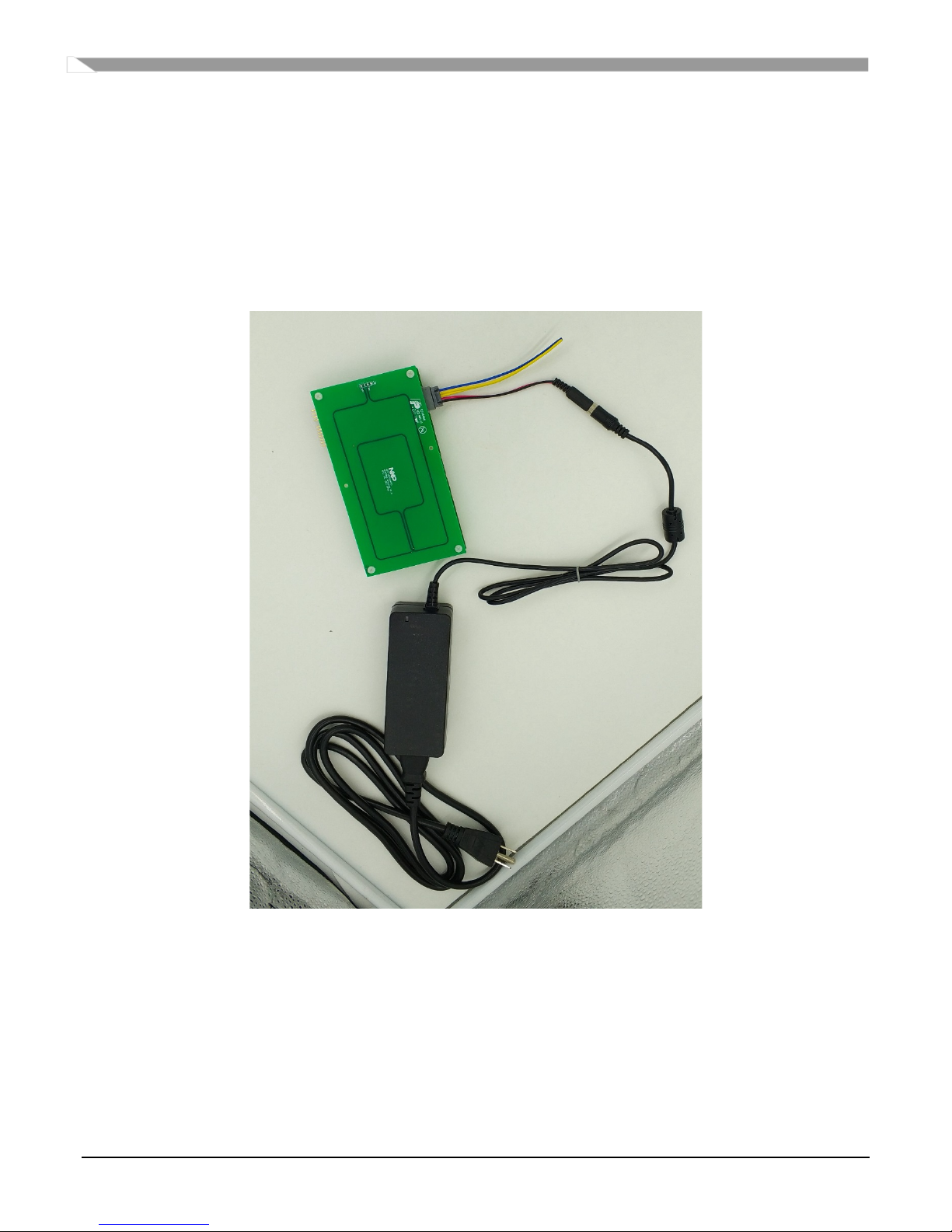
2.1 Pack content
1. WCT Automotive MP-A9 (WCT-15WTXAUTO) demo board
2. Power supply connector
3. Power supply 12V/3A
WCT1011A/WCT1013A Automotive MP-A9 Wireless Charging Application User’s Guide, Rev. 0, 10/2017
2 NXP Semiconductors
Figure 1 Hardware pack contents
Page 3
2.2 Board description
The WCT board is connected to the system by the main power connector. It comprises the automotive
battery connection (red wire = +12 V line, black wire = GND line), the CAN connection (yellow wires),
and the IGNITION (blue wire).
The connectors on the bottom edge of the board provide a JTAG connection for programming and
debugging, 2xSCI for the FreeMASTER tool connection for the debug option and the console connection,
and the temperature connector and backup touch sense connector are placed on the edge of the board. The
thermal resistor circuits can be used to develop the temperature sensing and protection.
The circuitry on the board is covered by the metal shield to lower the EMI and provides a f ixed position for
the coils. Figure 2 shows the device.
WCT1011A/WCT1013A Automotive MP-A9 Wireless Charging Application User’s Guide, Rev. 0, 10/2017
NXP Semiconductors 3
Figure 2 Device
Page 4
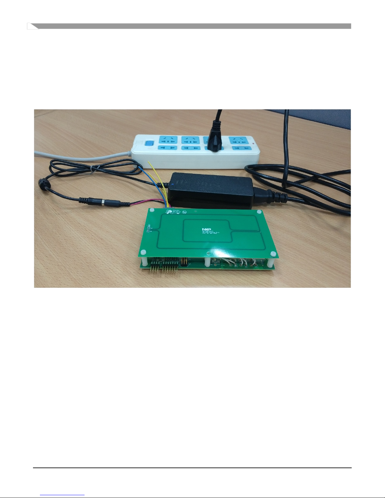
2.3 Powering on a board
To power on a board, perform the following steps:
1. Plug power supply 12 V to the socket.
2. Plug the power supply connector into the board.
3. Connect power supply 12 V and power supply connector.
Figure 3 Power supply components
WCT1011A/WCT1013A Automotive MP-A9 Wireless Charging Application User’s Guide, Rev. 0, 10/2017
4 NXP Semiconductors
Page 5

2.4 Hardware setup for FreeMASTER and Console communication
Console FreeMaster
R47
10.0K
V3.3
RXD0
RXD1
TXD 1
R210
10.0K
TXD 0
J2
HDR_2X4_RA
1 2
3
4
6
5
7 8
To set up the hardware for FreeMASTER and Console communication, perform the following steps:
1. Find two UART-to-USB adaptor boards, and successfully install this UA RT-to-USB device driver
on the computer. The virtual serial port on the computer should work well.
2. Plug the USB-UART converting board to SCI connector J2 according to the SCH signal pin
position. The two channels of UART are for different purposes: FreeMASTER and Console.
WCT1011A/WCT1013A Automotive MP-A9 Wireless Charging Application User’s Guide, Rev. 0, 10/2017
NXP Semiconductors 5
Figure 4 SCIs and JTAG connectors
Page 6

3. Application Operation
Connect the demo to the supply voltage +12 V DC. The WCT starts to send pe riodically the power ping to
check whether the compatible device wireless charging receiver (WCR) is placed on the charging surface.
When the Qi-compliant device is placed on the top of the TX coils area, the WCT starts the charging
process. If there is no correct Qi answer from the WCR side, the TX does not start the Qi charging process.
If the WCR answers properly, the power transfer starts. The actual level of the transferred power is
controlled by the WCT in accordance with WCR requirements. The receiver sends messages to the WCT
through ASK on the coil resonance power signal, and the transmitter sends the information to the receiver
by FSK according to the Qi specif ication. The power transfer is terminated if the receiver is removed from
the WCT magnetic field.
The system supports all Qi WCR devices: Qi_Ver-1.0 compliance and Qi_Ver-1.1 compliance, and the Qi
EPP 15 W receiver. The sy stem supports all the FOD features for different receivers. For the low-power 5
W receiver, the power loss FOD is supported. For the EPP 15 W receiver, both Q-value method and power
loss FOD method are supported.
WCT1011A/WCT1013A Automotive MP-A9 Wireless Charging Application User’s Guide, Rev. 0, 10/2017
6 NXP Semiconductors
Page 7
4. Hardware Description
BCM
Coil Selection
Full Bridge
Rail
Voltage
C
o
i
l
0
400nF
C
o
i
l
1
C
o
i
l
2
DDM
RC circuits
pack5
Q fator
detection
Input Voltage
Temperature
Sampling Circuit
Buck-boost
Digital /
analog
control
MOS DRIVER
WCT1011/3A
NFC
CAN
CONSOLE
FreeMaster
VIN
DCDC
VOUT
CAR battery
VIN
LDO
VOUT
Coil current
Q-voltage
WPC DDM
Q-resonance
Resonant Circuits
5V/0.3A
3.3V/0.2A
Inverter Current/
voltage
FB Inverter
Coil Switched
Digital buck-boost
Input Current
Input EMI filter
Can and Lin
NFC NCF3340
WCT1011/3A
UART&JTAG
Q-value detection
Figure 5 shows the block diagram of the automotive wireless charger MP-A9.
Go to the NXP website to obtain the latest Hardware Design files.
The whole design consists of several blocks, which are described in the following sections.
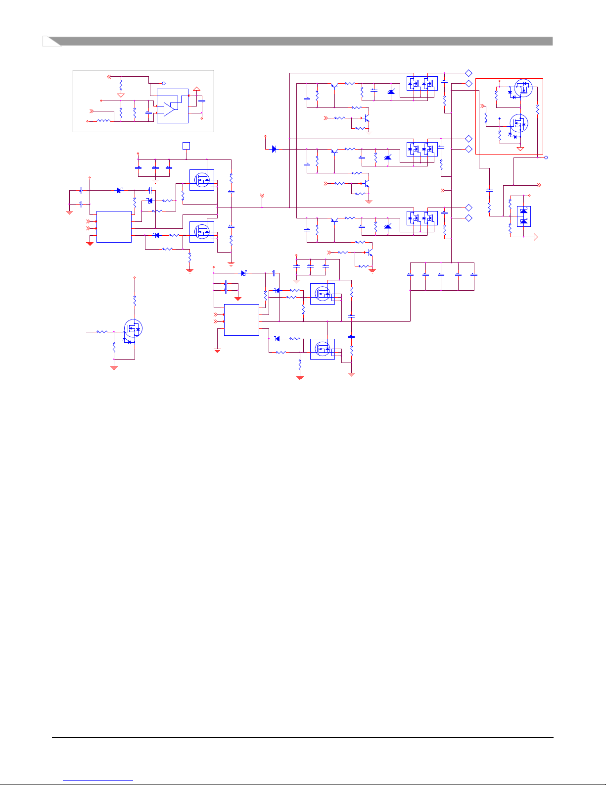
Figure 5 Block diagram of the automotive wireless charger MP-A9
WCT1011A/WCT1013A Automotive MP-A9 Wireless Charging Application User’s Guide, Rev. 0, 10/2017
NXP Semiconductors 7
Page 8
4.1 I nput EMI filter
C371
10uF
C311
0.1uF
50V
VRAIL_2
D84
PMEG060V050EPD
DNP
1
2
3
GND2
C496
47pF
C368
0.1uF
50V
Ipeak_S2
8
R442
0.015
C449 10uF
C448 10uF
GND2
GND2
GND2
GND2
GND2
GND2
Small board 2
D56
1PS76SB10
A C
D57
1PS76SB10
A
C
R400
10.0K
VDrive_S2
R401
10.0K
C305 0.1uF
C304 0.1uF
R402
10
R403 10
DBUCK_PWML_S2
8
DBUCK_PWMH_S2
8
R404 10
AUIRS2301S
U30
VCC
1
HIN
2
LIN
3
COM
4
LO
5
VS
6
HO
7
VB
8
Q51
NVTFS5820NLTAG
1
4
3
2
5
Q50
NVTFS5820NLTAG
1
4
3
2
5
Q52
NVTFS5820NLTAG
1
4
3
2
5
Q53
NVTFS5820NLTAG
1
4
3
2
5
R405
10.0K
R406
10.0K
VDrive_S2
C308 0.1uF
R408 10
C307 0.1uF
R407
10
DBOOST_PWML_S2
8
DBOOST_PWMH_S2
8
R409 10
L24
10UH
1
2
AUIRS2301S
U31
VCC
1
HIN
2
LIN
3
COM4LO
5
VS
6
HO
7
VB
8
VBAT_SW_2
C369
10uF
R411
3.32
C319
1000pF
C343
1000pF
C344
1000pF
C318
1000pF
R466
3.32
R410
3.32
R467
3.32
The input connector J1 provides the whole connection to the car wiring. It connects the battery voltage to
the WCT and CAN communication interface.
The input filter consists of the Common Mode Filter FL1 and the filter capacitors C1, C3, C4, C14, and
L1.
The main battery voltage switch is equipped with MOSFET Q1. This stage is controlled by the main
controller WCT1011A/WCT1013A and the IGNITION signal. The hardware overvoltage protection
(more than 20 V DC) is also implemented by D1 and Q2 to this switch.
4.2 System voltage DCDC and LDO
The 12 V Car Battery input is connected to a buck converter U25 (MPQ4558). Its output is 5 V and
supplies LDO U26 (MPQ8904), MOSFET Driver, and CAN Transceiver. The 3.3 V output of LDO is
mainly for WCT1011A/WCT1013A and other 3.3 V powered components.
Generally, the DCDC works at the light-load conditions. High efficiency in light-load is very important
for this auxiliary buck converter.
4.3 Rail voltage generated by digital buck-boost or analog buck-boost chip
The Qi specification for the MP-A9 topology requires the DC voltage control to control the power
transferred to the receiver. The buck-boost converter is selected to obtain the regulated DC voltage in the
range from 1 V DC to 24 V DC for the full-bridge inverter power supply. The buck-boost can be digitally
controlled by the WCT chip or the individual analog buck-boost converter and the WCT chip just controls
the output voltage feedback.
Digital buck-boost module includes the drivers, the full-bridge converter, and the output voltage feedback.
The DCDC converter’s control loop is implemented by the firmware, and the control parameters can be
optimized with different main circuit parameters, such as the inductor and output capacitor.
WCT1011A/WCT1013A Automotive MP-A9 Wireless Charging Application User’s Guide, Rev. 0, 10/2017
8 NXP Semiconductors
Figure 6 Digital buck-boost main circuits
Page 9
For the analog buck-boost module, the LTC3789 is selected to generate the rail voltage. The WCT chip
C524 0.01uF
GND6
R664
1K
R665
1K
R666 68K
C525 1000pF
C526 3300pF
R6670
R6680
DNP
R669
120K
R671 0
R672 0
DNP
C527
10uF
R676
0.015
GND6
GND6
C529 0.22uF
INTVCC
9
C530 4.7uF
GND6
C531 0.22uF
GND6
VBAT_SW_6
R6790
GND6
INTVCC
9
INTVCC
9
GND6
R646
2.00k
R687
2.00k
LTC3789IGN
U75
VFB
1
SS
2
SENSE+3SENSE-
4
ITH
5
SGND
6
MODE/PLLIN
7
FREQ
8
RUN
9
VINSNS
10
VOUTSNS
11
ILIM
12
IOSENSE+
13
IOSENSE-
14
TRIM
15
SW2
16
TG2
17
BOOST2
18
BG2
19
EXTVCC
20
INTVCC
21
VIN
22
BG1
23
PGND
24
BOOST1
25
TG1
26
SW1
27
PGOOD
28
GND6
R6570
DCDC_PG_6
9
GND6
R6700
VRAIL_6
R625
1.6K
C502
10uF
GND6
C503
10uF
GND6
C504
10uF
GND6
R680 0
VBAT_SW_6
C513
47pF
VRAIL_6
TP64
DNP
Differential Wire
Small board 6
DCDC_EN_6
9
GND6
R634 10
R635 10
D90 1PS76SB10
A
C
R637 10
R636 10
R639 0
R638 0
D91
1PS76SB10
AC
R641 0
R640 0
R642 0
R643
0
C515
0.1uF
50V
R6450
D85
PMEG2005AEA
AC
D86
PMEG2005AEA
AC
D87
PMEG2005AEA
AC
D88
PMEG2005AEA
A
C
C518
0.1uF
50V
R651
0.015
R652
10.0K
R653
10.0K
Q76
NVTFS5820NLTAG
1
4
3
2
5
Q77
NVTFS5820NLTAG
1
4
3
2
5
R654
10.0K
Q78
NVTFS5820NLTAG
1
4
3
2
5
R655
10.0K
Q79
NVTFS5820NLTAG
1
4
3
2
5
L32
10UH
1
2
VBAT_SW_6
C521
0.1uF
50V
VRAIL_6
INTVCC
9
R662
200
C523
4700pF
RAIL_CNTL_6
9
INTVCC
9
R663
39K
R661 4.3K
GND6
R629 100
DNP
R628 100
DNP
VRAILB_S6
C514 1.0uF
IS-_S6
9
R677
100
R678
100
C517
2700pF
C520
2700pF
C519
2700pF
C516
2700pF
R648
3.32
R647
3.32
R650
3.32
R649
3.32
controls the rail voltage by one analog signal. This analog signal affects the analog buck-boost converter
feedback, and then the system can get the rail voltage as the system expects.
The digital buck-boost is recommended for use on this wireless charging solution due to its lower cost,
simpler hardware circuits, and easier to be controlled.
4.4 Full-bridge and resonant circuits
The full-bridge power stage consists of two MOSFET Drivers, U8 and U9, as well as four power
MOSFETs, Q13, Q15, Q19, and Q20. The MOSFET Drivers are powered by the stable voltage level 5 V
DC that decreases the power losses in the drivers and MOSFETs. The full-bridge power stage converts the
variable DC voltage VRAIL to the square wave 50% duty-cycle voltage with 125 kHz frequency. The
range of the used frequency (120 kHz to 130 kHz) is defined in the Qi specification for the MP-A9
topology.
The resonant circuits consist of C111, C112, C423, C580, and coils, all of which are fixed values defined
in the Qi specification for the MP-A9 topology. The snubber RC pairs connected in parallel to power
MOSFETs are used to lower the high frequency EMI products. The Vrail discharge circuit Q46, R376, is
switched ON while the system is terminated.
WCT1011A/WCT1013A Automotive MP-A9 Wireless Charging Application User’s Guide, Rev. 0, 10/2017
NXP Semiconductors 9
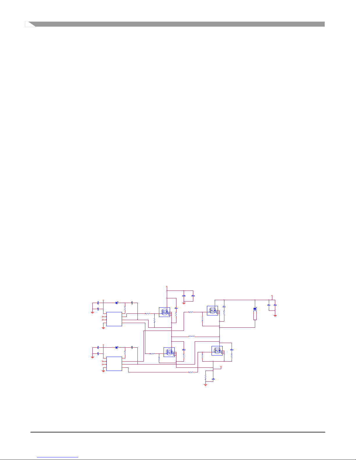
Figure 7 Analog buck-boost main circuits
Page 10
C364
22uF
C578
1000PF
R752
51
R751
51
C44
1000PF
R753
51
C579
1000PF
COIL2
Q81
2N7002BKW
1
2 3
Q82
BSS84W
1
2 3
R683
6.8K
C423
0.1uF
R682
100K
R684
100K
C112
0.1uF
C111
0.1uF
C580
0.1uF
C582
0.1uF
DNP
R805
2.00k
D9
BZT52H-C16
A C
D17
BZT52H-C16
A C
D13
BZT52H-C16
A C
R573 1.5K
R575 1.5K
R574 1.5K
COIL1
COIL0
FOD
AC Coil Current
VBAT_SW
R80 5.11K
D14
BAT54SW
1 2
3
R98 5.11K
R88 5.11K
R116
5.11K
R81
33.2K
COILS
R90
33.2K
COIL0_EN
3
TP16
DNP
TP18
DNP
TP17
DNP
TP19
DNP
COIL1_EN
3
SW_GATE0
Q9
IPG20N10S4L-22
241
3
6
5
SW_GATE1
Q12
IPG20N10S4L-22
241
3
6
5
COIL2_EN
3
R101 33.2K
TP20
DNP
TP21
DNP
SW_GATE2
COILS
6
R95
7.5K
Q16
IPG20N10S4L-22
241
3
6
5
R74
7.5K
R84
7.5K
C101
0.022uF
C105
0.022uF
C439
4700pF
C109
0.022uF
C440
4700pF
C441
4700pF
V3.3A
DDM
AC_COIL_CURRENT_OP
3
GAIN_SWITCH
3
TP65
DNP
V3.3A
R118
3.9K
R224
51K
D42
BAS16H
A C
Q14
PMBT4401
2 3
1
Q10
PMBT4401
2 3
1
Q18
PMBT4401
2 3
1
Q8
PMBTA92
1
2 3
R73
5.11K
Q11
PMBTA92
1
2 3
Q17
PMBTA92
1
2 3
TP35
DNP
C210
4700pF
100V
R83
5.11K
R94
5.11K
C499
1.0uF
IS-
8
L7
2.9OHM
1 2
TP49
DNP
+
-
OUT
IN+
IN-
V+
GND
REF
U21
INA214AQDC KRQ1
1
2
3
4
5
6
R514
0.015
VRAIL
VRAILA
R76
0.015
C94
0.1uF
R79
10.0K
INPUT_CURRENT
3,5
FOD
Inverter Input Current
V3.3A
R376
100
R278
10.0K
VDriv e
R279
10.0K
R201 0
R426
0
HB1A
6
C108
1000pF
C107
1000pF
R89 4.7
R91 4.7
C104 0.1uF
R87
3.32
C181 0.1uF
R85
10
HB1A
R92
3.32
Q13
NVTFS5820NLTAG
1
4
3
2
5
TP7
DNP
1
D12
1PS76SB10
A C
VRAILA
Q15
NVTFS5820NLTAG
1
4
3
2
5
D59
PMEG2005AEA
AC
D25
PMEG2005AEA
AC
C96
0.1uF
50V
C97
0.1uF
50V
C444 4.7uF
AUIRS2301S
U8
VCC
1
HIN
2
LIN
3
COM
4
LO
5
VS
6
HO
7
VB
8
COIL_PWM_HL
3
COIL_PWM_HH
3
VDriv e
R281
10.0K
R280
10.0K
R428 0
C120
1000pF
R427 0
R105 4.7
C121
1000pF
R102 4.7
C118 0.1uF
HB1B
R99
10
C183 0.1uF
R106
3.32
R100
3.32
D18
1PS76SB10
A C
VRAILA
COIL_PWM_LH
3
COIL_PWM_LL
3
Q20
NVTFS5820NLTAG
1
4
3
2
5
Q19
NVTFS5820NLTAG
1
4
3
2
5
D61
PMEG2005AEA
A
C
D60
PMEG2005AEA
AC
AUIRS2301S
U9
VCC
1
HIN
2
LIN
3
COM
4
LO
5
VS
6
HO
7
VB
8
C445 4.7uF
R365
100k
R681
2.00k
Q46
2N7002BKW
1
2 3
VRAILA
C98
22uF
R77 20K
R86 20K
C99
22uF
R97 20K
C100
22uF
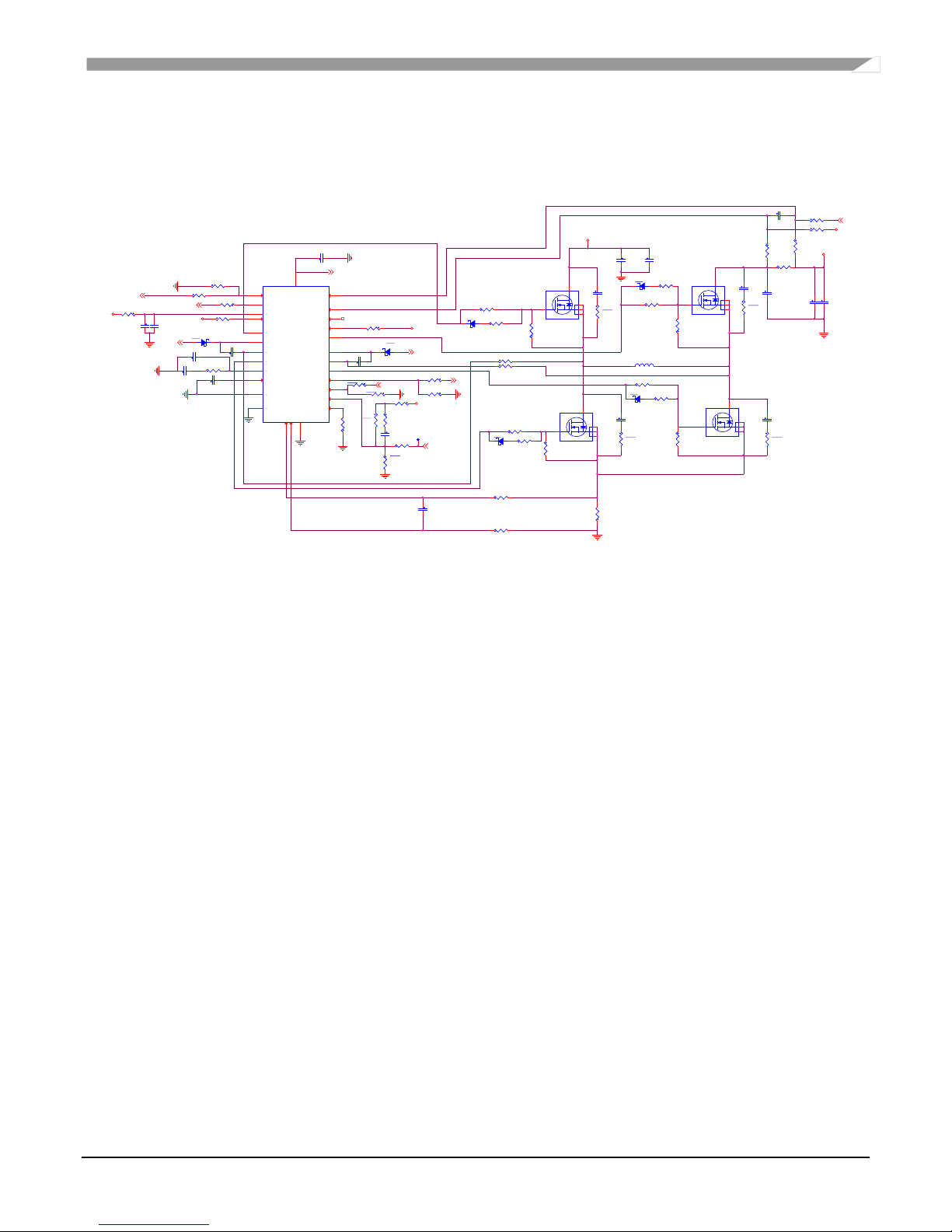
Figure 8 Full bridge circuits and coil selection circuits
4.5 Communication
There is bi-way communication between the medium power transceiver and receiver. Communication
from RX to TX: The receiver measures the received power and sends back to transmitter the information
about the re quired power level. This message is amplitude modulated (AM) on the coil current and sensed
by TX.
The RC circuits (C210, R116, R118, R224), known as DDM, sample the signals from the coil, compress
the signal amplitude, and feed to ADC B-channel of WCT1011A/WCT1013A. The information about the
current amplitude and modulated data are processed by the embedded software routine.
Communication from TX to RX: TX shall negotiate with RX in the negotiation phase if requested by RX.
TX uses FSK Modulation to communicate with RX, and the communication frequency is about 512 times
operating frequency.
4.6 FOD based on power loss
The power loss
Received Power , i.e.
in Figure 9.
WCT1011A/WCT1013A Automotive MP-A9 Wireless Charging Application User’s Guide, Rev. 0, 10/2017
10 NXP Semiconductors
, which is defined as the difference between the Transmitted Power and the
=
, provides the power absorption in Foreign Objects, as shown
Page 11
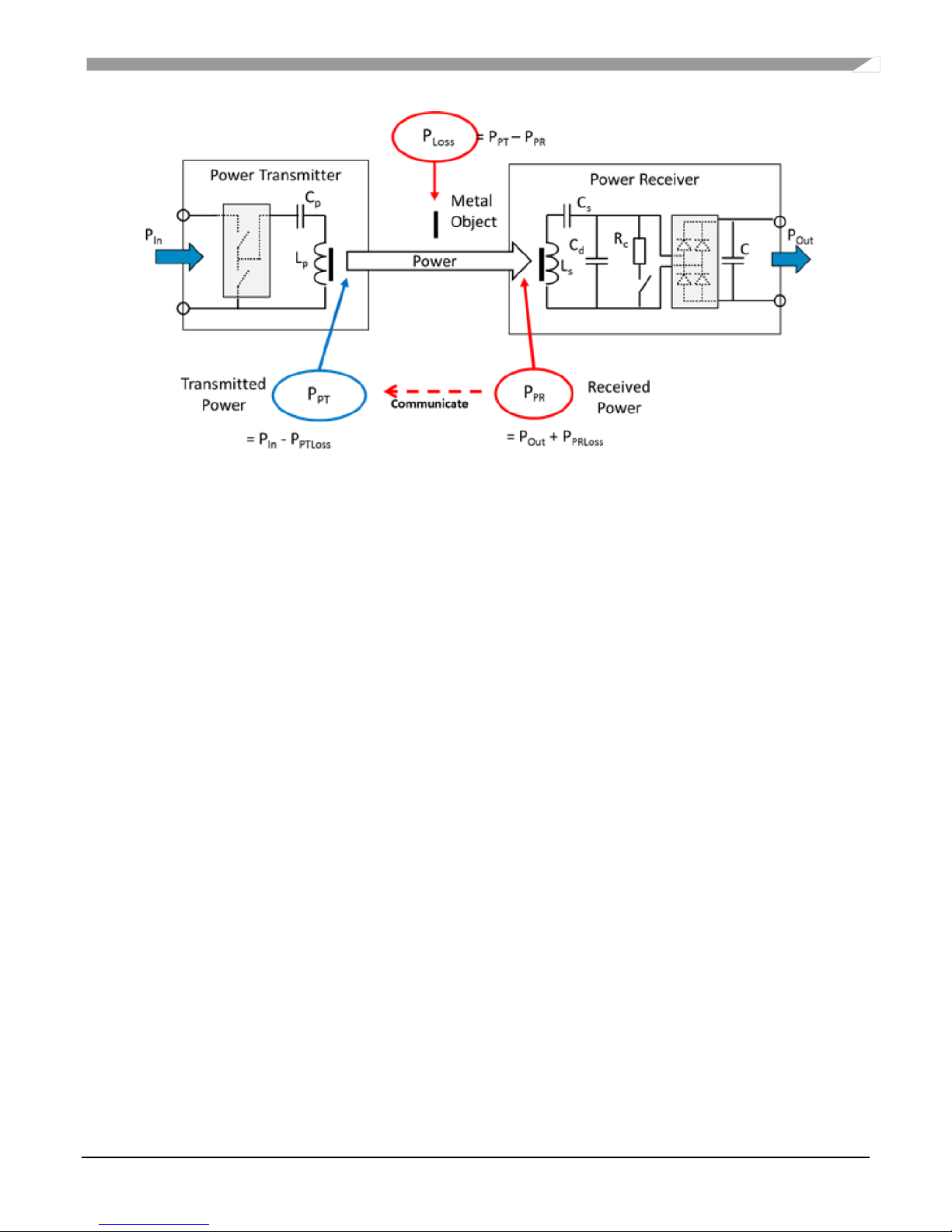
Figure 9 Power loss illustrated
When the FO is implemented in the power transfer, the power loss will increase accordingly, and the FO
can be detected based on the power loss method.
Power loss FOD method is divided into two types: FOD for baseline power profile (TX and RX can
transfer no more than 5 W of power) and extensions power profile (TX and RX can transfer power above
5 W).
4.6.1 Power loss FOD baseline
The equation for power loss FOD baseline is
The Transmitted Power represents the amount of power that leaves the TX due to the magnetic field
of the TX, and
=
, where represents the input power of the TX and
power dissipated inside the TX. could be measured by sampling input voltage and input current, and
could be estimated through the coil current.
The Received Power represents the amount of power that is dissipated within the RX due to the
magnetic field of the TX, and
is the power lost inside the RX.
=
+
When NXP WCT-15WTXAUTO charges the RX baseline, the power loss baseline is applied. The TX
continuously monitors
, and if it exceeds the threshold several times, the TX terminates power
transfer.
=
. The power
.
is provided at the RX’s output and
is the
4.6.2 Power loss FOD extensions
Typically, a RX estimates the power loss inside itself to determine its Received Power. Similarly, the TX
estimates the power loss inside itself to determine its Transmitted Power. A systematic bias in these
WCT1011A/WCT1013A Automotive MP-A9 Wireless Charging Application User’s Guide, Rev. 0, 10/2017
NXP Semiconductors 11
Page 12

estimates results in a difference between the Transmitted Power and the Received Power, even if there is
no Foreign Object present on the Interface Surface. To increase the effectiveness of the power loss
method, the TX can remove the bias in the calculated power loss by calibration. For this purpose, the TX
and Power RX execute the calibration phase before the power transfer phase starts. The TX needs to verify
that there is no FO present on its interface surface before the calibration phase and FOD based on Q factor
could work.
As the bias in the estimates can be dependent on the power level, the TX and RX determine their
Transmitted Power and Received Power at two load conditions — a “light” load and a “connected” load.
The “light” load is close to the minimum expected output power, and the “connected” load is close to the
maximum expected output power. Based on the two load conditions, the Power Transmitter can calibrate
its Transmitted Power using linear interpolation. Alternatively, the Power Transmitter can calibrate the
reported Received Power.
Take calibrated Transmitted Power as an example:
b =
()
a =
=
()
()
()
()
+
()
()
(
()
)
()
Therefore, the TX uses the calibrated Transmitted Power to determine the power loss as follows:
=
When a RX baseline is charged by NXP WCT-15WTXAUTO, only the power loss FOD baseline works.
If a RX extension is placed on NXP WCT-15WTXAUTO, the Q factor would be measured at first to
detect if there is a FO presents. If yes , the TX would stop charging; otherwise, the TX can proceed to
calibration phase and power transfer phase, and power loss FOD extension works to detect if a FO is
inserted during power transfer phase.
For details of FOD, see the WCT1011A /WCT1013A Automotive MP-A9 Run-Time Debug User’s Guide
(WCT101XARTDUG).
4.7 FOD based on Q factor change
A change in the environment of the TX coil typically causes its inductance to decrease or its equivalent
series resistance to increase. Both effects lead to a decrease of the TX coil’s Q factor. The RX sends a
packet including the reference Q factor for TX to compare and determine if FO exists, as shown in
Figure 10.
The reference Q factor is defined as the Q factor of Test Power Transmitter #MP1’s Primary Coil at an
operating frequency of 100 kHz with RX positioned on the interf ace surface and no FO nearby. Due to the
differences between its design and that of Test Power Transmitter #MP1, the difference between the
frequency it uses to determine its Q factor and 100 kHz, the TX needs to convert the Q factor it measured
WCT1011A/WCT1013A Automotive MP-A9 Wireless Charging Application User’s Guide, Rev. 0, 10/2017
12 NXP Semiconductors
Page 13
to that of Test Power Transmitter #MP1. NXP provides the conversion method and needs to get the
parameters on board at first. The TX would do auto-calibration and get parameters at the first time
powering up after flashed new image, and then these parameters are written to flash. Therefore, it is
necessary to make sure there is no object on the TX surface at the first time powering up after flashed new
image.
Figure 10 Quality factor threshold example
4.7.1 Free Resonance Q factor
The free resonance Q factor detection is to detect the decay rate of the resonance signal, as shown in
Figure 11. With the system’s high Q, driving just a few pulses near resonant frequency are sufficient to
serve as impulses and start the sy stem ringing. Collec t ADC data of tank voltage ( or coil current), and then
get the decay rate of the signal.
Q=/(-ln(Rate))
Rate is the value of decay rate of resonance signal.
WCT1011A/WCT1013A Automotive MP-A9 Wireless Charging Application User’s Guide, Rev. 0, 10/2017
NXP Semiconductors 13
Page 14

TP23
DNP
C407
330pF
C406
330pF
D53
BAT54SW
1 2
3
R371
221K
R372
221K
V3.3A_Q
COILS
5
Q_RESONANCE_VOLT
3
V3.3A_Q
R531
100
R532
100
-
+
U28C
LMV824-N-Q1
10
9
8
C271
27PF
Figure 11 Resonance signal
The circuit for free resonance Q measurement is as shown in the following figure, which samples the
signal on resonance capacitors.
Figure 12 Free resonance Q measurement circuit
4.8 Coil selection
The Qi specification defines the MP-A9 as the more-than-one coil topology with one coil energized at a
time to realize the free position charging.
The coil selection topology connects only one coil to the full-bridge inverter at a time. The coil is equipped
with the dual N-MOSFETs, Q9, Q12, or Q16, controlled by the WCT1011A/WCT1013A controller
through the control interface based on the low power bipolar transistors.
4.9 Analog sensing
Some ports of the ADC A-channel of WCT1011A/WCT1013A are used for sensing analog signals, such
as temperature, full-bridge input current, input voltage, and rail voltage.
WCT1011A/WCT1013A Automotive MP-A9 Wireless Charging Application User’s Guide, Rev. 0, 10/2017
14 NXP Semiconductors
Page 15
5. Application Monitoring and Control Through FreeMASTER
FreeMASTER is a user-friendly real-time debug monitor and data visualization tool for application
development and information management. Supporting nonintrusive variable monitoring on a running
system, FreeMASTER allows the data from multiple variables to be viewed in an evolving
oscilloscope-like display or in a common text for mat. The application can also be monitored and operated
from the web-page-like control panel.
5.1 Software setup
To set up the software, perform the following steps:
1. Install FreeMASTER V2.0.2 or later version from the NXP website: nxp.com/freemaster
2. Plug the USB-UART converting board to SCI connector J2, and connect the FreeMASTER
MicroUSB port to your computer.
3. Open the Device Manager, and check the number of the COM port.
4. Unpack the embedded source code to your local disk.
5. Start the FreeMASTER application by opening:
WCT1011A/WCT1013A Automotive MP-A9 Wireless Charging Application User’s Guide, Rev. 0, 10/2017
NXP Semiconductors 15
Figure 13 Device manager
Page 16
• MWCT1013A
<unpacked_files_location>/15W_MP/example/wct1013a/ wct1013A.pmp
• MWCT1011A
<unpacked_files_location>/15W_MP/example/wct1011a/ wct1011A.pmp
6. Choose Project –> Options.
Figure 14 Choosing Options
7. Ensure that the correct virtual Port (according to Step 3) and Speed are selected.
Figure 15 Setting Port and Spe ed
8. Ensure that the MAP file is correct. The default directories are as follows:
• MWCT1013A
WCT1011A/WCT1013A Automotive MP-A9 Wireless Charging Application User’s Guide, Rev. 0, 10/2017
16 NXP Semiconductors
Page 17
<unpacked_files_location>/15W_MP/build/demo/wct1013Ademo/demo_ldm_debug/wct1013A
demo_debug.elf
• MWCT1011A
<unpacked_files_location>/15W_MP/build/demo/wct1011Ademo/demo_sdm_debug/wct1011A
demo_debug.elf
Figure 16 Setting the MAP file
9. Connect FreeMASTER.
Power on MP-A9, and then start the communication by clicking the STOP button on the FreeMASTER
GUI.
Figure 17 Stop button
WCT1011A/WCT1013A Automotive MP-A9 Wireless Charging Application User’s Guide, Rev. 0, 10/2017
NXP Semiconductors 17
Page 18

5.2 Real-t ime application variables monitoring
FreeMASTER enables monitoring and updating all the application global variables. In this application,
several key variables are displayed in the scope windows. These variables are divided into differ ent blocks
as shown in the following figure.
Figure 18 Real-time application variables
• wct_debug
This block shows the variables used for the GUI command.
• Library
This block contains power loss variables, timing variables, coil selection variables, working
parameters, system status, DDM variables, and RX information.
• HAL
This block contains ADC raw data and DDM buffer values.
• NVM
This block lists all NVM parameters. Q factor sub-block shows the Q factor calibration constants.
RRQD sub-block shows the quick removal calibration constants. FOD sub-block shows the FOD
characterization calibration constants. Normalization sub-block shows the FOD normalization
constants. Analog sub-block shows the rail voltage calibration constants.
• LIB PARAMS
This block lists all parameters used for the WCT library.
• Command
WCT1011A/WCT1013A Automotive MP-A9 Wireless Charging Application User’s Guide, Rev. 0, 10/2017
18 NXP Semiconductors
Page 19

The command variable is used to stop WCT, start WCT, and do auto-calibration.
• QFactor
This block contains the variables for Q factor detection.
• Test
This block contains some variables for debugging.
• Protection
This block contains protection variables, such as input voltage protection, input current protection, and
temperature protection.
• KeyFOB
This block contains the variables used for KeyFob.
NOTE
Besides the variables above, all the global variables can be added to
FreeMASTER. The procedure to generate and add variables to watch
window is described in the FreeMASTER user manual.
5.3 Appl ic ation parameters modification
The application parameters (NVM parameters) can be easily viewed and changed on the control panel.
The control panel contains the web page elements (buttons, check boxes, and text fields) that enable a
user-friendly way to visualize and change the application control parameters.
WCT1011A/WCT1013A Automotive MP-A9 Wireless Charging Application User’s Guide, Rev. 0, 10/2017
NXP Semiconductors 19
Page 20

Figure 19 Application variables
The application variables are divided into three tabs:
• System Params – group of general system parameters.
• Coil Params – enables access to the variables related to the coils control
• Calibration – group of parameters for calibration of the input current, input voltage, and foreign
objects detector
The meaning of each parameter is described next to the text field.
NOTE
• Some parameters of System Params and Coil Params are not used
for MP-A9. The used parameters are described in
WCT1011A/WCT1013A Automotive MP-A9 Run-Time User’s
Guide.
• The parameters of Calibration can be changed at run-time. But the
parameters of System Params and Coil Params cannot take effect
immediately. These parameters should be saved to project, rebuild
project, and re-flash the board.
WCT1011A/WCT1013A Automotive MP-A9 Wireless Charging Application User’s Guide, Rev. 0, 10/2017
20 NXP Semiconductors
Page 21

6. Application Monitoring Through Console
The application sends some information and error states through SCI to the console. The information is
sent when the board is turned on, when the device is charging, or in case of some error state.
For digital buck-boost platform, only one SCI port (SCI0) is available. SCI0 is used for FreeMASTER by
default. Users select an alternative method to enable the debug console.
1. Disable FreeMASTER and configure SCI0 as the debug console.
a) #define DEBUG_CONSOLE_SUPPORTED (TRUE)
#define FREEMASTER_SUPPORTED (FASLE)
The macros are defined in example->wct101xa–>configure-> appcfg.h.
b) #define QSCI_CONSOLE_INDEX 0
#define QSCI_FREEMASTER_INDEX 1
The macros are defined in example->wct101xa->driver->qsci.h
c) gWCT_Params.tDebugConfig.bGeneralDbg = 1;
This variable is in wct_LibPar am s. c.
2. Change FreeMASTER communication interface to JTAG and configure SCI0 as the debug console.
a) #define DEBUG_CONSOLE_SUPPORTED (TRUE)
#define FREEMASTER_SUPPORTED (TRUE)
The macros are defined in example->wct101xa–>configure-> appcfg.h.
b) #define QSCI_CONSOLE_INDEX 0
#define QSCI_FREEMASTER_INDEX 1
The macros are defined in example->wct101xa->driver->qsci.h
c) #define FMSTR_USE_SCI 0 /* To select SCI communication interface */
#define FMSTR_USE_JTAG 1 /* 56F8xxx: use JTAG interface */
The macros are defined in example->wct101xa–>configure-> freemaster_cfg.h.
d) gWCT_Params.tDebugConfig.bGeneralDbg = 1;
This variable is in wct_LibPar am s. c.
6.1 Software setup
1. Plug the USB-UART converting board to SCI connector J2, and connect the console MicroUSB
port to the computer.
2. Open Device Manager, and check the number of the COM port.
WCT1011A/WCT1013A Automotive MP-A9 Wireless Charging Application User’s Guide, Rev. 0, 10/2017
NXP Semiconductors 21
Page 22

Figure 20 Device Manager
3. Run the communication program supporting console, such as HyperTerminal or RealTerm.
4. The following table shows the communication setup.
Table 1 Port configurations
Port number Serial port from Device Manager
Baud 19200
Data Bits 8
Stop Bits 1
Parity None
Hardware Flow Control None
Display As ASCII
5. Open the port or start communication, which depends on the used Terminal.
WCT1011A/WCT1013A Automotive MP-A9 Wireless Charging Application User’s Guide, Rev. 0, 10/2017
22 NXP Semiconductors
Page 23

7. Programming New Software and Calibration
Users are provided with a software package, which includes a WCT1011A/WCT1013A project and a Bin
file (.elf or .S). Users can flash alternative to the board. After flashing new software, board calibration
must be carried out.
7.1 I nst all CodeWarrior 10.7
1. Download installation files.
For proper installation of CodeWarrior 10.7, install both CodeWarrior for Microcontrollers
10.7 and CodeWarrior for MCUs v10.7 service pack.
Access the following webpage and log in:
https://www.nxp.com/products/developer-resources/software-development-tools/codewarrior-de
velopment-tools/codewarrior-development-suites/codewarrior-development-suite-special:CW-S
UITE-SPECIAL?tab=Design_Tools_Tab
Click Download for CodeWarrior Special Edition (offline or online).
Figure 21 Clicking Download for CodeWarrior Special Edition
Download CodeWarrior for Microcontrollers 10.7 service pack from the following link.
https://www.nxp.com/products/power-management/wireless-charging-ics/15-watt-wireless-charg
ing-transmitter-ics-for-automotive-applications:MWCT1x1xA?tab=Design_Tools_Tab
WCT1011A/WCT1013A Automotive MP-A9 Wireless Charging Application User’s Guide, Rev. 0, 10/2017
NXP Semiconductors 23
Page 24

Figure 22 Downloading CodeWarrior for MCU v10.7 service pack
2. Double-click CW_MCU_v10.7_b160721_SE.exe after downloading.
Figure 23 Setup file
3. Make sure that DSC is selected.
WCT1011A/WCT1013A Automotive MP-A9 Wireless Charging Application User’s Guide, Rev. 0, 10/2017
24 NXP Semiconductors
Figure 24 DSC installed
Page 25

4. Launch CodeWarrior, create a folder workspace, and select it as the default workspace.
Figure 25 Workspace Launcher dialog box
5. Choose Help –> Install New Software.
Figure 26 Install New Software
WCT1011A/WCT1013A Automotive MP-A9 Wireless Charging Application User’s Guide, Rev. 0, 10/2017
NXP Semiconductors 25
Page 26

6. Click Add and Archive, and then select the
mcu10_7.Wireless_Charging_MWCT101x.win.sp.v1.0.1.zip file.
Figure 27 Selecting the update pack
WCT1011A/WCT1013A Automotive MP-A9 Wireless Charging Application User’s Guide, Rev. 0, 10/2017
26 NXP Semiconductors
Page 27

7. Select MCU v10.7 DSC Service Packs, and then click Next.
Figure 28 Selecting service packs
8. Review the license terms. If you agree with the license terms, select I accept the terms of the
license agreement, and then click Finish.
Figure 29 Installation finished
WCT1011A/WCT1013A Automotive MP-A9 Wireless Charging Application User’s Guide, Rev. 0, 10/2017
NXP Semiconductors 27
Page 28

7.2 Boar d and programmer connection
Connect the 14-pin debug cable to J4 of the board (notice pin-1 position of cable).
Figure 30 Connecting the debug cable to th e board
7.3 Program the project files
1. Import a project.
Right-click in the CodeWarri or Pro je cts window and choose Import to import an existing
project, as shown in the following figures. If the CodeWarrior Projects window is not displayed,
open it through Window -> Show View -> CodeWarrior Projects.
WCT1011A/WCT1013A Automotive MP-A9 Wireless Charging Application User’s Guide, Rev. 0, 10/2017
28 NXP Semiconductors
Figure 31 Importing a project (1)
Page 29

Figure 32 Importing a project (2)
Select the project directory, as show in this figure.
WCT1011A/WCT1013A Automotive MP-A9 Wireless Charging Application User’s Guide, Rev. 0, 10/2017
NXP Semiconductors 29
Figure 33 Importing a project (3)
Page 30

Select WCT1013A project.
Figure 34 Importing a project (4)
2. Build a project.
Select build configurations by clicking the project name in the project window shown in the
following figure. The demo_ldm_debug build contains debug information. The
demo_ldm_release is same with demo_ldm_debug except debug information.
WCT1011A/WCT1013A Automotive MP-A9 Wireless Charging Application User’s Guide, Rev. 0, 10/2017
30 NXP Semiconductors
Page 31

Figure 35 Building a project (1)
Right-click wct1013Ademo, and then choose Clean Project and Build Project.
3. Download the project.
Download the project from the Debug drop-down list or form Run -> Debug. In Download
Configurations, select a download configuration according to your build configurations and
debugger type, USB TAP, PnE Multilink, or OSJTAG.
WCT1011A/WCT1013A Automotive MP-A9 Wireless Charging Application User’s Guide, Rev. 0, 10/2017
NXP Semiconductors 31
Figure 36 Clean Project and Build Project
Page 32

Figure 37 Downloading the project
After the project is downloaded, the MCU stops at the startup code. Press the Run button or F8 to
let MCU run. Make sure that there is no object on the TX surface before making MCU run. Due to
the auto-calibration for rail voltage, Q-factor, and quick removal will be done at the first-time the
TX runs after flashed image.
WCT1011A/WCT1013A Automotive MP-A9 Wireless Charging Application User’s Guide, Rev. 0, 10/2017
32 NXP Semiconductors
Figure 38 Project Downloaded
Page 33

7.4 Program the Bin file (.elf or .S)
1. Choose Flash Programmer –> Flash File to Target.
Figure 39 Choosing Flash File to Target
2. Click New to create a new connection.
Figure 40 Creating a new connection
WCT1011A/WCT1013A Automotive MP-A9 Wireless Charging Application User’s Guide, Rev. 0, 10/2017
NXP Semiconductors 33
Page 34

3. In the Name text box, enter a connection name (any name is OK), and click New to create a target.
Figure 41 Entering a connection name
4. In the Name text box, enter a target name (any name is OK but cannot be same with the connection
name), and choose dsc.MWCT101x -> MWCT1013A from the Target Type drop-down list.
Figure 42 Choosing MWCT1013A
5. Select Execute reset and Initialize target, set the initialization target file path to the CW
installation folder, and then select MWCT1013A.tcl.
WCT1011A/WCT1013A Automotive MP-A9 Wireless Charging Application User’s Guide, Rev. 0, 10/2017
34 NXP Semiconductors
Page 35

Figure 43 Executing reset and initia lizing target
WCT1011A/WCT1013A Automotive MP-A9 Wireless Charging Application User’s Guide, Rev. 0, 10/2017
NXP Semiconductors 35
Page 36

6. Click the Memory tab. Select Memory configuration, set the memory configuration file path to
the CW installation folder, and then select MWCT1013A.mem. Click Finish.
Figure 44 Memory configuration
WCT1011A/WCT1013A Automotive MP-A9 Wireless Charging Application User’s Guide, Rev. 0, 10/2017
36 NXP Semiconductors
Page 37

7. Select USB TAP for the Connection type, and then click Finish.
Figure 45 Setting the connection type
8. Set the Bin file path to be File to Flash. Select Save the Target Task for future programming.
Power on MP-A9 and click Erase and Program.
9. Select the task path to save the task.
WCT1011A/WCT1013A Automotive MP-A9 Wireless Charging Application User’s Guide, Rev. 0, 10/2017
NXP Semiconductors 37
Figure 46 Erase and Program
Page 38

Figure 47 Selecting the task path
10. When program is finished, the Console window displays the following log.
Figure 48 Programming finished log
11. For future programming, just select FLASH MPA9 and wait until the programming is finished.
Figure 49 Future programming
WCT1011A/WCT1013A Automotive MP-A9 Wireless Charging Application User’s Guide, Rev. 0, 10/2017
38 NXP Semiconductors
Page 39

7.5 Pro gram by boot loader
Boot loader is completely independent of the application codes, and it can reside in flash forever after
downloading an application code. When a system is reset, the boot loader starts to run. After a boot delay
in seconds, the boot loader jumps to the programmed application code, even without receiving the
application S-record file. When receiving the application S-record file, the boot loader programs the
application code to the on-chip flash. After completion, the boot loader jumps to the application startup
code.
1. The boot loader code is not flashed to the board by default. Download the boot loader code. Import
the boot loader project and follow the steps described in Section 7.3 to download the project.
Figure 50 Boot loader project
2. Generate an application S-record fil e.
Enable the boot loader function. Set the following macro to TRUE in appcfg.h.
#define BOOTLOADER_USED (TRUE)
Follow the figure below to configure the application project settings. Select the option Sort by
Address. Set Max S-Record Length to a value that does not exceed 255. Select DOS (\\r\\n) for
S-Record EOL Character.
WCT1011A/WCT1013A Automotive MP-A9 Wireless Charging Application User’s Guide, Rev. 0, 10/2017
NXP Semiconductors 39
Page 40

Figure 51 Configure project settings
Recompile the project after completing the configuration above. The generated S-record file is in
<unpacked_files>\15W_MP\build\demo\wct1013Ademo\demo_ldm_debug for the WCT1013A
chip or <unpacked_files>\15W_MP\build\demo\wct1011Ademo\demo_sdm_debug for the
WCT1011A chip. The S-record file is the combined p and x S-record file without “.p” or “.x” in
the extension name (.s).
3. Download the application code by the boot loader.
Most serial terminal programs can be used to send an S-Record file from a host to the
WCT1011A/WCT1013A board through the boot loader. For example, Tera Term can be used in
the Windows platform.
SCI0 is used for communication. Plug the USB-UART convertor to the SCI connector J2 and the
computer. Open Tera Term, and then select Serial and Port. Check the COM port in the Device
Manager.
WCT1011A/WCT1013A Automotive MP-A9 Wireless Charging Application User’s Guide, Rev. 0, 10/2017
40 NXP Semiconductors
Page 41

Figure 52 Tera Term connection
Choose Setup -> Serial port to configure the COM properties as shown in Figure 54.
WCT1011A/WCT1013A Automotive MP-A9 Wireless Charging Application User’s Guide, Rev. 0, 10/2017
NXP Semiconductors 41
Figure 53 Serial port
Page 42

Figure 54 Serial port setup
Choose File -> Send file.
Figure 55 Send file
Select the application S-Record file and click Open.
WCT1011A/WCT1013A Automotive MP-A9 Wireless Charging Application User’s Guide, Rev. 0, 10/2017
42 NXP Semiconductors
Page 43

Figure 56 Send application S-Record file
The downloading progress is displayed in the Tera Term window. After downloading is
completed, the application code starts.
Figure 57 Download application S-Record file
WCT1011A/WCT1013A Automotive MP-A9 Wireless Charging Application User’s Guide, Rev. 0, 10/2017
NXP Semiconductors 43
Page 44

7.6 Board calibration
NXP provides the FreeMASTER GUI tool for calibration and parameters tuning. For board calibration,
see the WCT1011A/WCT1013A Automotive MP-A9 V3.1 Run-Time Debugging User’s Guide
(WCT101XAV31RTDUG).
WCT1011A/WCT1013A Automotive MP-A9 Wireless Charging Application User’s Guide, Rev. 0, 10/2017
44 NXP Semiconductors
Page 45

8. Software Description
8.1 Sof tware overview
8.1.1 Directory Structure
The following figure shows an example of the directory structure of the whole WCT1013A_MP-A9
distribution.
Figure 58 Directory structure of the whole WCT1013A_MP-A9 distribution
8.1.2 CodeWarrior Projects
There are four CodeWarrior projects in the package. The following figure shows all the four projects in
CodeWarrior GUI when all of them are imported.
Figure 59 CW projects
WCT1011A/WCT1013A Automotive MP-A9 Wireless Charging Application User’s Guide, Rev. 0, 10/2017
NXP Semiconductors 45
Page 46

Combined with different program models and different user cases, multiple build configurations are
predefined in respective projects.
There are two program models provided for WCT parts.
• Small Program Model: The compiler generates a more efficient switch table, when the code is in
the range 0x0-0xFFFF. This model is more efficient, but the code size is limited to 64 KB words.
• Larger Program Model: Extends DSP56800E addressing range by providing 24-bit address
capability to instructions. That allows user accesses beyond the 64 KB word boundary of 16-bit
addressing.
For WCT1011A, there are two build configurations:
• demo_sdm_debug: Small Program Model, including code for debugging.
• demo_sdm_release: Small Program Model, excluding debugging code to save memory size.
Figure 60 WCT1011A build configur ation
For WCT1013A, there are three build configurations:
• demo_ldm_debug: Large Program Model, including code for debugging.
• demo_ldm_release: Large Program Model, excluding debugging code to save memory size.
• nfc_demo_ldm_debug: NFC dedicated build configuration. Large Program Model, including code
for debugging.
NOTE
The full-featured NFC stack will be released in next version. The slim NFC
stack is ready. Contact NXP for the firmware with the NFC feature.
WCT1011A/WCT1013A Automotive MP-A9 Wireless Charging Application User’s Guide, Rev. 0, 10/2017
46 NXP Semiconductors
Page 47

Figure 61 WCT1013A build configuration
8.2 Func t ional description
NXP provides full-featured wireless charging functions on the reference board. If a certain function is not
needed, disable it by the definitions in the header file.
8.2.1 FreeMASTER
• FreeMASTER is supported. The following configuration is used to enable or disable it.
Configurations Default value Location Description
FREEMASTER_SUPPORTED TRUE appcfg.h Enables or disables the function. Set
• FreeMASTER communication interface configuration is in freemaster_cfg.h. SCI interface is
enabled and JTAG interface is disabled by default. Only one interface can be set at a time.
#define FMSTR_USE_SCI 1 /* To select SCI communication interface */
#define FMSTR_USE_JTAG 0 /* 56F8xxx: use JTAG interface */
• FreeMASTER SCI port is SCI0 by default.
1) #define FMSTR_SCI_BASE 0xE080 /* base address of SCI_0 */
The macro is in freemaster_cfg.h.
2) #define QSCI_FREEMASTER_INDEX 0 //QSCI0
The macro is in qsci.h.
Table 2 FreeMASTER configurations
TRUE to enable it. Set FALSE to
disable it.
8.2.2 Low power mode
Low power mode is supported. In the analog ping interval, the MCU enters LPSTOP mode and DCDC
module is closed. The following configuration is used to enable or disable it.
WCT1011A/WCT1013A Automotive MP-A9 Wireless Charging Application User’s Guide, Rev. 0, 10/2017
NXP Semiconductors 47
Page 48

Table 3 Low power mode configurations
Configurations Default value Location Description
LOW_POWER_MODE_ENABLE FALSE appcfg.h Enables or disables the function.
Set TRUE to enable it. Set FA LSE
to disable it.
8.2.3 Debug console
Debug console is supported. The following configuration is used to enable or disable it.
Table 4 Debug console configurations
Configurations Default value Location Description
DEBUG_CONSOLE_SUPPORTED FALSE appcfg.h Enables or disables the function.
Set TRUE to enable it. Set FA LSE
to disable it.
For WCT1011A/WCT1013A digital buck-boost platform, only one SCI port is available. This port is
default used for FreeMASTER. If debug console is used, disable FreeMASTER or change FreeMASTER
communication interface to JTAG. The configurations are described in Chapter 6.
8.2.4 Bootloader
Bootloader is supported. The following configuration is used to enable or disable it.
Table 5 Bootloader configurations
Configurations Default value Location Description
BOOTLOADER_USED FALSE appcfg.h Enables or disables the function. Set
TRUE to enable it. Set FALSE to
disable it.
If bootloader is used, download the bootloader project to the board. Then change BOOTLOADER_USED
to TRUE, rebuild application project, and download application .S file by bootloader.
8.2.5 DCDC control type
NXP provides two DCDC control types: digital buck-boost and analog buck-boost. The default one is
digital buck-boost. The following configuration is used to switch the DCDC control type.
Table 6 DCDC control type configurations
Configurations Default value Location Description
DIGITAL_BUCKBOOST TRUE appcfg.h Switch DCDC control type. Set TRU E to
enable digital buck-boost. Set FALSE to
enable analog buck-boost.
8.3 Pro t ection mechanisms
The following table lists the protections that can be implemented.
WCT1011A/WCT1013A Automotive MP-A9 Wireless Charging Application User’s Guide, Rev. 0, 10/2017
48 NXP Semiconductors
Page 49

Table 7 Protection mechanisms
Protection Default limits Variables Description
Rail voltage 23000 mV gPROT_Params.wMaxRailVol Application implemented. If the rail voltage
exceeds the limit, charging is turned off. The
limit value can be changed in PROT_Init().
Battery voltage Min: 8000 mV
Max: 18000
mV
Hysteresis:
1000 mV
Input current 4000 mA gPROT_Params.wMaxInputCurrent Application implemented. If the input current
Coil current 5000 mA gPROT_Params.wMaxCoilCurrent Application implemented. If the coil current
Input power Non power
transfer: 3000
mW
Power transfer:
240%
gPROT_Params.wMinBatteryVol
gPROT_Params.wMaxBatteryVol
gPROT_Params.wBatteryHystVol
gPROT_Params.wMaxInputPowerDuri
ngNonXfer
gPROT_Params.wMaxInputPowerMult
iPercent
Application implemented. If the battery
voltage exceeds the maximum, the WCT
library stops. When the battery voltage is
lower than the difference between maximum
and hysteresis, WCT library starts. When the
battery voltage is lower than the minimum,
the WCT library stops. When the battery
voltage is higher than the sum of the
minimum and hysteresis, the WCT library
starts.
The limit value can be changed in
PROT_Init().
exceeds the limit, charging is turned off. The
limit value can be changed in PROT_Init().
exceeds the limit, charging is turned off. The
limit value can be changed in PROT_Init().
Application implemented. When the TX is in
the PING phase, the maximum limit is 3000
mW by default. When the TX is in online
calibration (EPP RX), power transfer or
renegotiation phase, the maximum li mit is
240% of the RX maximum power. For BPP
RX, the maximum is 12 W. For EPP, the
maximum is 36 W. The limit value can be
changed in PROT_Init().
Temperature Max: 60℃
Hysteresis:
10℃
Safe digital ping 200 mA gPROT_Params.wSafeDigitalPingInpu
FOD BPP RX: 600
mW
EPP RX:
1000 mW
WCT1011A/WCT1013A Automotive MP-A9 Wireless Charging Application User’s Guide, Rev. 0, 10/2017
NXP Semiconductors 49
gPROT_Params.swTemperatureThres
hold
gPROT_Params.wTemperatureHyst
tCurrentThreshold
lFodParams.dwPowerLossLimit Library implemented. If the power loss
Application implemented. If the temperature
exceeds the maximum, the WCT library
stops. When the temperature is lower than
the difference between the maximum and
hysteresis, the WCT library starts. The limit
value can be changed in PROT_Init().
Library implemented. If the input current
sampled at the beginning of the digital ping
exceeds the limit, digital ping stops. The limit
value can be changed in PROT_Init().
exceeds the limit, charging is turned off for 5
minutes. The limit value can be changed in
WCT_GetFODParams().
Page 50

9. System Bring Up
9.1 Ping sequences
When low power mode is disabled and no receiver is placed on the charging surface, the ping sequence is
as follows:
Digital ping appears at about every 5 seconds and the analog ping appears at about every 400 ms. There
are 12 to 13 analog ping between two digital pings.
The following figures show the PWM waveforms of the ping sequence and ping patterns.
Figure 62 Digital ping interval
WCT1011A/WCT1013A Automotive MP-A9 Wireless Charging Application User’s Guide, Rev. 0, 10/2017
50 NXP Semiconductors
Page 51

Figure 63 Analog ping interval
WCT1011A/WCT1013A Automotive MP-A9 Wireless Charging Application User’s Guide, Rev. 0, 10/2017
NXP Semiconductors 51
Figure 64 Digital ping pattern
Page 52

Figure 65 Analog ping pattern
9.2 LED indicat ion
The default LED display modes for different TX working states are shown in the following table.
Table 8 LED display modes
LED No.
LED 1 (Red) Off Blink Off On On On
LED 2 (Green) Blink On On Off Off Off
Standby Charging Charging
LED operational status
FOD fault TX fault RX fault
complete
The display pattern can be changed in WCT_UpdateDevUsrIndication().
9.3 Debug messages
The system is able to print messa ges from a specified SCI por t to inform users about what ha ppened in the
system. That may be helpful for users to understand the system working procedure and debug issues.
Message: ID, T/O
Print information when identification packet times out.
Message: EXT ID, T/O
Prints information when extended identification packet times out.
Message: CFG, HOLDOFF Invalid
Prints information when hold off time is out of range.
WCT1011A/WCT1013A Automotive MP-A9 Wireless Charging Application User’s Guide, Rev. 0, 10/2017
52 NXP Semiconductors
Page 53

Message: CFG, Incorrect Count, Count1 (Count2)
Prints information when the amount of optional configuration packets received does not match the number
in the configuration packet.
• Count 1: the number in configuration packet
• Count 2: TX received optional configuration packets amount
Message: CFG, Over CP
Prints information when the RX power is beyond capability.
Message: CFG, Rcvd 0xXX
Prints the packet type that should not be received in the configuration phase.
Message: CFG, T/O
Prints information when the configuration packet times out.
Message: XFER, INCOMP
Prints information when the RX version is not compatible.
Message: XFER, RCVPWR T/O
Prints information when receive power packet times out.
Message: XFER, PLoss T/O
Prints information when FOD happens.
Message: PROP, <Packet type>
Prints the proprietary packet header.
Message: XFER, Rcvd 0xXX Reset
Prints the packet type that should not be received in power transfer phase. Charging is reset.
WCT1011A/WCT1013A Automotive MP-A9 Wireless Charging Application User’s Guide, Rev. 0, 10/2017
NXP Semiconductors 53
Page 54

Message: XFER, Rcvd 0xXX
Revision number
Date
Substantive changes
0
10/2017
Initial release
Prints the packet type that is not defined in WPC specification.
10. Revision History
The following table provides the revision history.
Table 6 Revision history
WCT1011A/WCT1013A Automotive MP-A9 Wireless Charging Application User’s Guide, Rev. 0, 10/2017
54 NXP Semiconductors
Page 55

nxp.com
nxp.com/support
Information in this document is provided solely to enable system and software
implementers to use NXP products. There are no express or implied copyright licenses
granted hereunder to design or fabricate any integrated circuits based on the information
in this document. NXP reserves the right to make changes without further notice to any
products herein.
NXP makes no warranty, representation, or guarantee regarding the suitability of its
products for any particular purpose, nor does NX
application or use of any product or circuit, and specifically disclaims any and all liability,
including without limitation consequential or incidental damages. “Typical” parameters
that may be provided in NXP dat
different applications, and actual performance may vary over time. All operating
parameters, including “typicals,” must be validated for each customer application by
customer’s technical experts. NXP does n
nor the rights of others. NXP sells products pursuant to standard terms and conditions of
sale, which can be found at the following address:
NXP, the NXP logo, Freescale, the Freescale logo are trademarks of NXP B.V. All other
product or service names are the property of their respective owners.
© 2017 NXP
How to Reach Us:
Home Page:
Web Support:
P assume any liability arising out of the
a sheets and/or specifications can and do vary in
ot convey any license under its patent rights
nxp.com/SalesTermsandConditions.
B.V.
Document Number: WCT101XAV31AUG
Rev. 3.1
10/2017
 Loading...