

Page 1
UM11111
PCAL6416AEV test board user manual
Rev. 1.0 — 12 April 2018 User manual
Document information
Information Content
Keywords PCAL6416AEV, OM13260, OM13320, OM13303
Abstract This user manual describes how to use NXP's PCAL6416AEV test board.
Page 2

NXP Semiconductors
UM11111
PCAL6416AEV test board user manual
UM11111 All information provided in this document is subject to legal disclaimers. © NXP B.V. 2018. All rights reserved.
User manual Rev. 1.0 — 12 April 2018
2 / 16
Revision history
Rev Date Description
v.1 20180412 Initial version
Page 3

NXP Semiconductors
UM11111
PCAL6416AEV test board user manual
UM11111 All information provided in this document is subject to legal disclaimers. © NXP B.V. 2018. All rights reserved.
User manual Rev. 1.0 — 12 April 2018
3 / 16
1 Introduction
This user manual describes how to use NXP's PCAL6416AEV test board. This board is
designed for testing functional characteristics of the PCAL6416AEV part, saving time for
NXP customer qualification of the 16-bit Agile GPIO expander. This board works with
NXP's Fm+ demo board (OM13260) or any customer I2C-bus controller. It has a socket
for VFPGA24 3x3 mm, a 14-pin connector for FM+ demo board using 3.3V, and two
external power supply TPs for VDDI and VDDP of the PCAL6416AEV, as well as an I2Cbus header for customer I2C controller.
2 Features and benefits
• Direct connection to OM13320 Fm+ Development kit
• External I2C-bus connection
• Isolated power rail for power measurement
• Socket of VFPGA24 3x3 mm with 0.30 mm ball size
• Flexible power supply configuration: 3.3V or external supply
• Direct connection to OM13303 GPIO Target board for I/O visualization
• Jumper configuration of device I2C address
• LED indicators for power and INT
• Scope ground connection loop
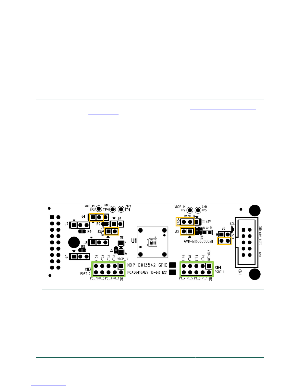
3 Hardware description
1. Socket U1 for VFBGA24 3x3 mm with 0.30 mm ball size packet
2. Connection to Fm+ demo board (OM13260) port A, B, C or D: CN2 is a 2x8 female
connector
3. Slave device address selection: J6 is a 2x2 male header
a. Slave device address = 0x010-0001(42h) when 1-2 is connected
b. Slave device address = 0x010-0000(40h) when 3-4 is connected
4. VDDI power selection: J4 is a 1x3 header. This jumper header is for selection VDDI
(I2C and internal logic power). The power is from Fm+ demo board 3.3V or external
power from TP3
a. VDDI = TP3 (VDDI_IN: external power) when J4 is opened and J5 is connected
b. VDDI = 3.3V from Fm+ demo board when J4: 1-2 is connected and J5 is
connected
c. VDDI = 5V from Fm+ demo board when J8: 1-2 & J4: 2-3 are connected and J5 is
connected
5. VDDP (IO port) power selection: J1 is a 1x3 header. This jumper header is for
selection VDDP (IO port power). The power is from Fm+ demo board 3.3V or external
power form TP2.
a. VDDP = TP2 (VDDP_IN: external power) when J1 is opened and J3 is connected
b. VDDP = 3.3V from Fm+ demo board when J1: 2-3 is connected and J3 is
connected
c. VDDP = 5V from Fm+ demo board when J8: 1-2 & J1: 1-2 is connected and J3 is
connected
6. VDDI external power input by TP3 (VDDI_IN) and TP4 (GND)
7. VDDP external power input by TP2 (VDDP_IN) and TP5 (GND)
8. External I2C SDA signal input from CN1 (SDA: Beagle master)
Page 4
NXP Semiconductors
UM11111
PCAL6416AEV test board user manual
UM11111 All information provided in this document is subject to legal disclaimers. © NXP B.V. 2018. All rights reserved.
User manual Rev. 1.0 — 12 April 2018
4 / 16
9. External I2C SCL signal input from CN2 (SCL: Beagle master)
10.CN3 and CN4 are 2x5 female headers connected to OM13303 GPIO Target board for
I/O visualization
11.LED power for INT(D1) signal and VPP(D2) power indicator
12.J2 is Reset jumper for PCAL6416AEV
4 Using NXP PCAL6416AEV with Fm+ demo board
1. Get I2C Fm+ Development Board Kit package at: http://www.nxp.com/demoboard/
OM13320.html
2. Connect CN2 of NXP PCAL6416AEV to any port A, B, C or D on Fm+ demo board
3. Set jumpers:
• J1 = 2-3 for +3V3 for VDDP_IN
• J3 = enabling power for VDDP
• J4 = 1-2 for +3V3 for VDDI_IN
• J5 = enabling power for VDDI
• J6 = 3-4 for PCAL6416AEV slave address = 0x010-0000 (40h)
4. Set jumpers:
• Use multi-meter at J3 for VDDP and J5 for VDDI
5. Test GPIO outputs and Interrupt
a. Put jumper on J4:1-2 & J5 to enable power of D1 LED indicators for INT and PWR
b. Connect OM13303GPIO Target Boards (Fm+ demo board kit) to CN3 and CN4
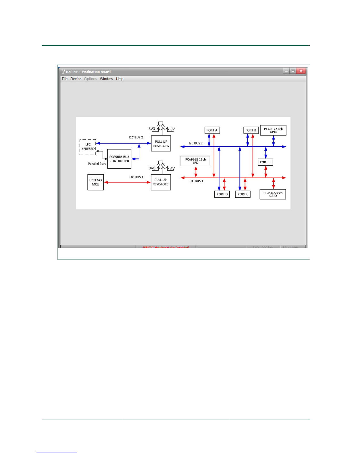
c. Connect USB from Fm+ demo board to the PC with NXP Fm+ software
Figure 1. Connect USB from Fm+ demo board
6. Use NXP Fm+ GUI software:
a. Open NXP Fm+ software
Page 5
NXP Semiconductors
UM11111
PCAL6416AEV test board user manual
UM11111 All information provided in this document is subject to legal disclaimers. © NXP B.V. 2018. All rights reserved.
User manual Rev. 1.0 — 12 April 2018
5 / 16
Figure 2. Open NXP Fm+
b. Go to Device Selection > I/O Expanders > 16-bit I/O Expanders > PCAL6416A
Page 6

NXP Semiconductors
UM11111
PCAL6416AEV test board user manual
UM11111 All information provided in this document is subject to legal disclaimers. © NXP B.V. 2018. All rights reserved.
User manual Rev. 1.0 — 12 April 2018
6 / 16
Figure 3. Go to device selection
c. Change Slave Address to 0x40 and make sure the Slave presence light is on
Page 7

NXP Semiconductors
UM11111
PCAL6416AEV test board user manual
UM11111 All information provided in this document is subject to legal disclaimers. © NXP B.V. 2018. All rights reserved.
User manual Rev. 1.0 — 12 April 2018
7 / 16
Figure 4. Change slave address to 0x40
d. The I/Os can be configured at input or output, input polarity changed, and output
set high or low.
Page 8

NXP Semiconductors
UM11111
PCAL6416AEV test board user manual
UM11111 All information provided in this document is subject to legal disclaimers. © NXP B.V. 2018. All rights reserved.
User manual Rev. 1.0 — 12 April 2018
8 / 16
Figure 5. Configure I/Os
I/O interrupt status, interrupt mask enable/disable and input latch enable/disable.
Page 9

NXP Semiconductors
UM11111
PCAL6416AEV test board user manual
UM11111 All information provided in this document is subject to legal disclaimers. © NXP B.V. 2018. All rights reserved.
User manual Rev. 1.0 — 12 April 2018
9 / 16
Figure 6. I/O interrupt status
If the port is set at output then that output port can change the drive strength.
Page 10

NXP Semiconductors
UM11111
PCAL6416AEV test board user manual
UM11111 All information provided in this document is subject to legal disclaimers. © NXP B.V. 2018. All rights reserved.
User manual Rev. 1.0 — 12 April 2018
10 / 16
Figure 7. Output port
5 Using NXP PCAL6416AEV with customer system
1. Connect input power for VDDI and VDDP
a. VDDI power is for I2C-bus and internal logic of PCAL6416AEV. VDDI can be input
from external power by TP3.
b. VDDP power is for I/O ports of PCAL6416AEV. VDDP can be input from external
power by TP2.
2. Set jumpers:
• J1 = open for external power for VDDP_IN
• J3 = enable power for VDDP
• J4 = open for external power for VDDI_IN
• J5 = enable power for VDDI
• J6 = 3-4 for PCAL6416AEV slave address = 0x010-0000
• TP2 = external power 3.3V for VDDP_IN with TP5 (GND)
• TP3 = external power 3.3V for VDDI_IN with TP4 (GND)
3. Test current of VDDI and VDDP
• Use multi-meter at J3 for VDDP and J5 for VDDI.
4. Test GPIO outputs and Interrupt
a. Put jumper on J4 to enable power of D1 LED indicators for INT and PWR
Page 11

NXP Semiconductors
UM11111
PCAL6416AEV test board user manual
UM11111 All information provided in this document is subject to legal disclaimers. © NXP B.V. 2018. All rights reserved.
User manual Rev. 1.0 — 12 April 2018
11 / 16
b. Connect OM13303 GPIO Target Boards to CN3 and CN4
c. Output Low to make the LED light turn on, output high to make LED light turn off
Figure 8. Test GPIO outputs and interrupt
Page 12

NXP Semiconductors
UM11111
PCAL6416AEV test board user manual
UM11111 All information provided in this document is subject to legal disclaimers. © NXP B.V. 2018. All rights reserved.
User manual Rev. 1.0 — 12 April 2018
12 / 16
6 Layout
Figure 9.
Page 13

NXP Semiconductors
UM11111
PCAL6416AEV test board user manual
UM11111 All information provided in this document is subject to legal disclaimers. © NXP B.V. 2018. All rights reserved.
User manual Rev. 1.0 — 12 April 2018
13 / 16
7 Notes
Page 14

NXP Semiconductors
UM11111
PCAL6416AEV test board user manual
UM11111 All information provided in this document is subject to legal disclaimers. © NXP B.V. 2018. All rights reserved.
User manual Rev. 1.0 — 12 April 2018
14 / 16
8 Legal information
8.1 Definitions
Draft — The document is a draft version only. The content is still under
internal review and subject to formal approval, which may result in
modifications or additions. NXP Semiconductors does not give any
representations or warranties as to the accuracy or completeness of
information included herein and shall have no liability for the consequences
of use of such information.
8.2 Disclaimers
Limited warranty and liability — Information in this document is believed
to be accurate and reliable. However, NXP Semiconductors does not
give any representations or warranties, expressed or implied, as to the
accuracy or completeness of such information and shall have no liability
for the consequences of use of such information. NXP Semiconductors
takes no responsibility for the content in this document if provided by an
information source outside of NXP Semiconductors. In no event shall NXP
Semiconductors be liable for any indirect, incidental, punitive, special or
consequential damages (including - without limitation - lost profits, lost
savings, business interruption, costs related to the removal or replacement
of any products or rework charges) whether or not such damages are based
on tort (including negligence), warranty, breach of contract or any other
legal theory. Notwithstanding any damages that customer might incur for
any reason whatsoever, NXP Semiconductors’ aggregate and cumulative
liability towards customer for the products described herein shall be limited
in accordance with the Terms and conditions of commercial sale of NXP
Semiconductors.
Right to make changes — NXP Semiconductors reserves the right to
make changes to information published in this document, including without
limitation specifications and product descriptions, at any time and without
notice. This document supersedes and replaces all information supplied prior
to the publication hereof.
Suitability for use — NXP Semiconductors products are not designed,
authorized or warranted to be suitable for use in life support, life-critical or
safety-critical systems or equipment, nor in applications where failure or
malfunction of an NXP Semiconductors product can reasonably be expected
to result in personal injury, death or severe property or environmental
damage. NXP Semiconductors and its suppliers accept no liability for
inclusion and/or use of NXP Semiconductors products in such equipment or
applications and therefore such inclusion and/or use is at the customer’s own
risk.
Applications — Applications that are described herein for any of these
products are for illustrative purposes only. NXP Semiconductors makes
no representation or warranty that such applications will be suitable
for the specified use without further testing or modification. Customers
are responsible for the design and operation of their applications and
products using NXP Semiconductors products, and NXP Semiconductors
accepts no liability for any assistance with applications or customer product
design. It is customer’s sole responsibility to determine whether the NXP
Semiconductors product is suitable and fit for the customer’s applications
and products planned, as well as for the planned application and use of
customer’s third party customer(s). Customers should provide appropriate
design and operating safeguards to minimize the risks associated with
their applications and products. NXP Semiconductors does not accept any
liability related to any default, damage, costs or problem which is based
on any weakness or default in the customer’s applications or products, or
the application or use by customer’s third party customer(s). Customer is
responsible for doing all necessary testing for the customer’s applications
and products using NXP Semiconductors products in order to avoid a
default of the applications and the products or of the application or use by
customer’s third party customer(s). NXP does not accept any liability in this
respect.
Export control — This document as well as the item(s) described herein
may be subject to export control regulations. Export might require a prior
authorization from competent authorities.
Evaluation products — This product is provided on an “as is” and “with all
faults” basis for evaluation purposes only. NXP Semiconductors, its affiliates
and their suppliers expressly disclaim all warranties, whether express,
implied or statutory, including but not limited to the implied warranties of
non-infringement, merchantability and fitness for a particular purpose. The
entire risk as to the quality, or arising out of the use or performance, of this
product remains with customer. In no event shall NXP Semiconductors, its
affiliates or their suppliers be liable to customer for any special, indirect,
consequential, punitive or incidental damages (including without limitation
damages for loss of business, business interruption, loss of use, loss of
data or information, and the like) arising out the use of or inability to use
the product, whether or not based on tort (including negligence), strict
liability, breach of contract, breach of warranty or any other theory, even if
advised of the possibility of such damages. Notwithstanding any damages
that customer might incur for any reason whatsoever (including without
limitation, all damages referenced above and all direct or general damages),
the entire liability of NXP Semiconductors, its affiliates and their suppliers
and customer’s exclusive remedy for all of the foregoing shall be limited to
actual damages incurred by customer based on reasonable reliance up to
the greater of the amount actually paid by customer for the product or five
dollars (US$5.00). The foregoing limitations, exclusions and disclaimers
shall apply to the maximum extent permitted by applicable law, even if any
remedy fails of its essential purpose.
Translations — A non-English (translated) version of a document is for
reference only. The English version shall prevail in case of any discrepancy
between the translated and English versions.
8.3 Trademarks
Notice: All referenced brands, product names, service names and
trademarks are the property of their respective owners.
Page 15

NXP Semiconductors
UM11111
PCAL6416AEV test board user manual
UM11111 All information provided in this document is subject to legal disclaimers. © NXP B.V. 2018. All rights reserved.
User manual Rev. 1.0 — 12 April 2018
15 / 16
Figures
Fig. 1. Connect USB from Fm+ demo board ................ 4
Fig. 2. Open NXP Fm+ ................................................ 5
Fig. 3. Go to device selection ...................................... 6
Fig. 4. Change slave address to 0x40 ......................... 7
Fig. 5. Configure I/Os ................................................... 8
Fig. 6. I/O interrupt status ............................................ 9
Fig. 7. Output port ...................................................... 10
Fig. 8. Test GPIO outputs and interrupt ..................... 11
Fig. 9. .......................................................................... 12
Page 16

NXP Semiconductors
UM11111
PCAL6416AEV test board user manual
Please be aware that important notices concerning this document and the product(s)
described herein, have been included in section 'Legal information'.
© NXP B.V. 2018. All rights reserved.
For more information, please visit: http://www.nxp.com
For sales office addresses, please send an email to: salesaddresses@nxp.com
Date of release: 12 April 2018
Document identifier: UM11111
Contents
1 Introduction ......................................................... 3
2 Features and benefits .........................................3
3 Hardware description ......................................... 3
4 Using NXP PCAL6416AEV with Fm+ demo
board .................................................................... 4
5 Using NXP PCAL6416AEV with customer
system ................................................................ 10
6 Layout .................................................................12
7 Notes .................................................................. 13
8 Legal information .............................................. 14
 Loading...