

Page 1

PCA9665
Fm+ parallel bus to I2C-bus controller
Rev. 02 — 7 December 2006 Product data sheet
1. General description
The PCA9665 serves as an interface between most standard parallel-bus
microcontrollers/microprocessors and the serial I2C-bus and allows the parallel bus
system to communicate bidirectionally with the I2C-bus. The PCA9665 can operate as a
master or a slave and can be a transmitter or receiver. CommunicationwiththeI2C-bus is
carried out on a Byte or Buffered mode using interrupt or polled handshake. The
PCA9665 controls all the I2C-bus specific sequences, protocol, arbitration and timing with
no external timing element required.
The PCA9665 has the same footprint as the PCA9564 with additional features:
• 1 MHz transmission speeds
• Up to 25 mA drive capability on SCL/SDA
• 68-byte buffer
2
• I
C-bus General Call
• Software reset on the parallel bus
2. Features
n Parallel-bus to I2C-bus protocol converter and interface
n Both master and slave functions
n Multi-master capability
n Internal oscillator trimmed to 15 % accuracy reduces external components
n 1 Mbit/s and up to 25 mA SCL/SDA IOL (Fast-mode Plus (Fm+)) capability
n I2C-bus General Call capability
n Software reset on parallel bus
n 68-byte data buffer
n Operating supply voltage: 2.3 V to 3.6 V
n 5 V tolerant I/Os
n Standard-mode and Fast-mode I2C-bus capable and compatible with SMBus
n ESD protection exceeds 2000 V HBM per JESD22-A114, 200 V MM per
JESD22-A115, and 1000 V CDM per JESD22-C101
n Latch-up testing is done to JEDEC Standard JESD78 which exceeds 100 mA
n Packages offered: DIP20, SO20, TSSOP20, HVQFN20
Page 2

NXP Semiconductors
PCA9665
Fm+ parallel bus to I2C-bus controller
3. Applications
n Add I2C-bus port to controllers/processors that do not have one
n Add additional I2C-bus ports to controllers/processors that need multiple I2C-bus ports
n Converts 8 bits of parallel data to serial data stream to prevent having to run a large
number of traces across the entire printed-circuit board
4. Ordering information
Table 1. Ordering information
T
=−40°C to +85°C
amb
Type number Topside
mark
PCA9665BS 9665 HVQFN20 plastic thermal enhanced very thin quad flat package;
PCA9665D PCA9665D SO20 plastic small outline package; 20 leads; body width 7.5 mm SOT163-1
PCA9665N PCA9665N DIP20 plastic dual in-line package; 20 leads (300 mil) SOT146-1
PCA9665PW PCA9665 TSSOP20 plastic thin shrink small outline package; 20 leads;
Package
Name Description Version
SOT662-1
no leads; 20 terminals; body 5 × 5 × 0.85mm
SOT360-1
body width 4.4 mm
PCA9665_2 © NXP B.V. 2006. All rights reserved.
Product data sheet Rev. 02 — 7 December 2006 2 of 91
Page 3
NXP Semiconductors
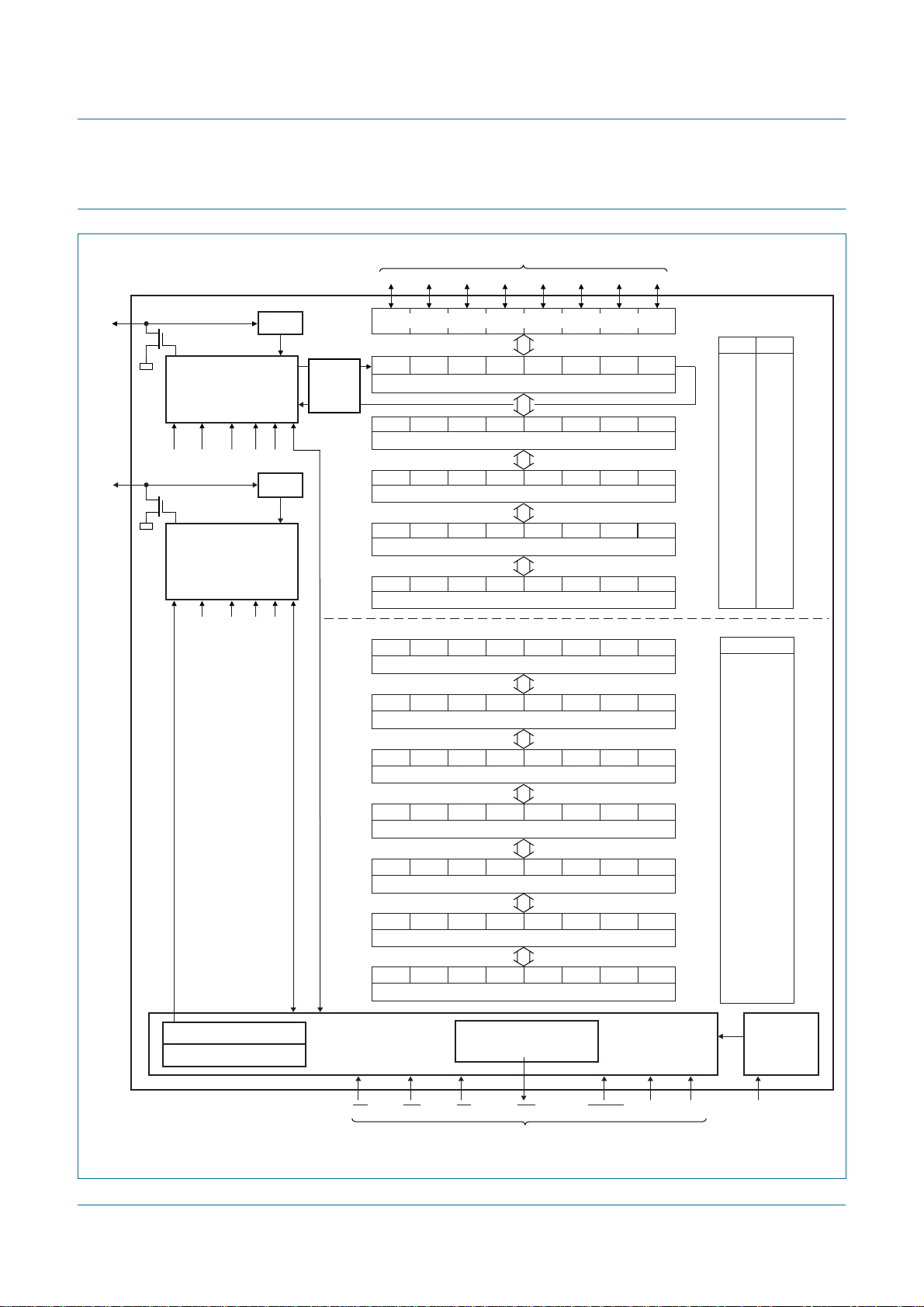
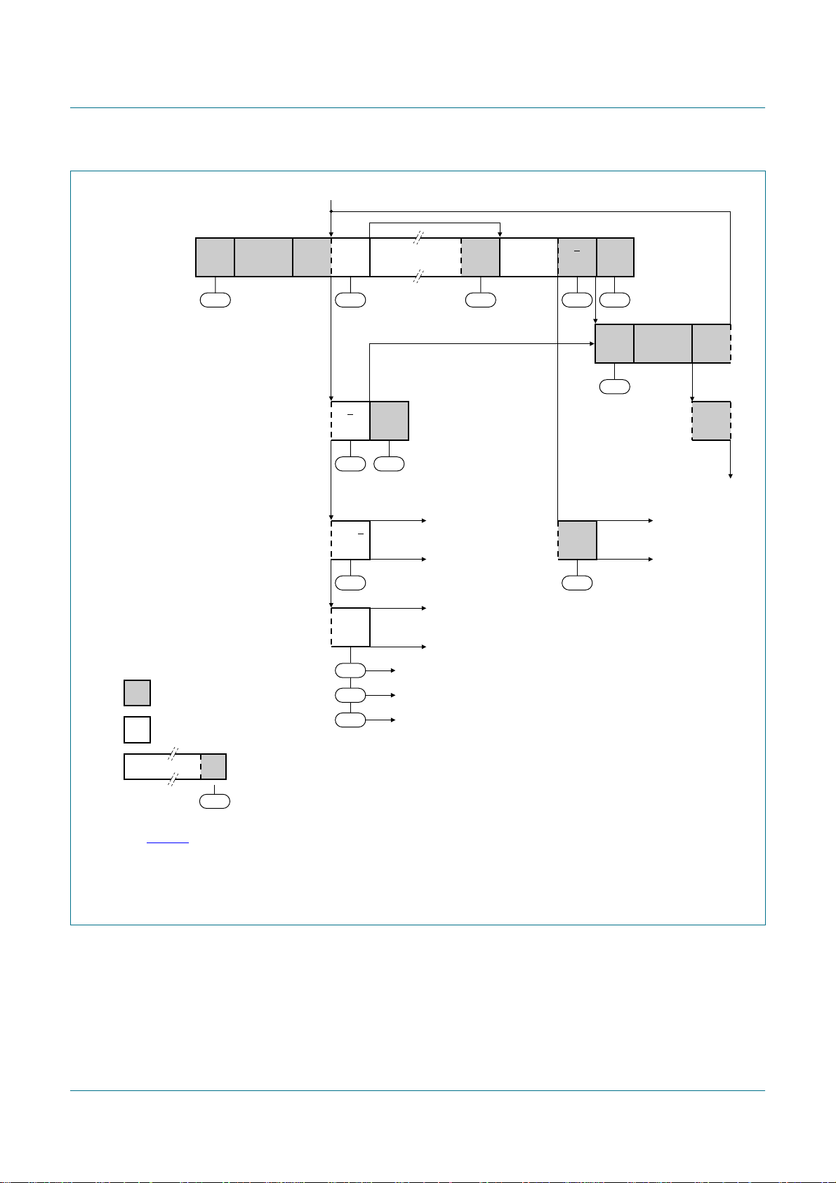
5. Block diagram
PCA9665
Fm+ parallel bus to I2C-bus controller
data
D7 D6 D5 D4 D3 D2 D1 D0
SDA
SCL
PCA9665
SDA CONTROL
AA ENSIO STA STOSI
SCL CONTROL
ENSIO STA STOSI
FILTER
FILTER
68-BYTE
BUFFER
BUS BUFFER
SD7 SD6 SD5 SD4 SD3 SD2 SD1 SD0
I2CDAT – data register – read/write
– – – – – IP2 IP1 IP0
INDPTR – indirect address pointer – write only
ST5 ST4 ST3 ST2 ST1 ST0 0 0
I2CSTA – status register – read only
AA ENSIO STA STO SI MODE
I2CCON – control register – read/write
BIT7 BIT6 BIT5 BIT4 BIT3 BIT2 BIT1 BIT0
INDIRECT – indirect register access – read/write
LB BC6 BC5 BC2 BC1 BC0
I2CCOUNT – byte count – read/write
AD7 AD6 AD5 AD4 AD3 AD2 AD1 GC
I2CADR – own address – read/write
L7 L6 L5 L4 L3 L2 L1 L0
I2CSCLL – SCL LOW period – read/write
BC4 BC3
– –
direct registers
A1 A0
01
00
00
11
10
indirect registers
INDPTR
00h
01h
02h
H7 H6 H5 H4 H3 H2 H1 H0
03h
04h
05h
06h
POWER-ON
RESET
002aab023
DD
CLOCK SELECTOR
OSCILLATOR
I2CSCLH – SCL HIGH period – read/write
TE BIT6 BIT5 BIT4 BIT3 BIT2 BIT1 BIT0
I2CTO – TIMEOUT register – read/write
IR7 IR6 IR5 IR4 IR3 IR2 IR1 IR0
I2CPRESET – software reset register – write only
– AC0
–––––AC1
I2CMODE – I
CE WR RD INT RESET A1 A0 V
2
C-bus mode register – read/write
INTERRUPT CONTROL
control signals
CONTROL BLOCK
Fig 1. Block diagram of PCA9665
PCA9665_2 © NXP B.V. 2006. All rights reserved.
Product data sheet Rev. 02 — 7 December 2006 3 of 91
Page 4
NXP Semiconductors
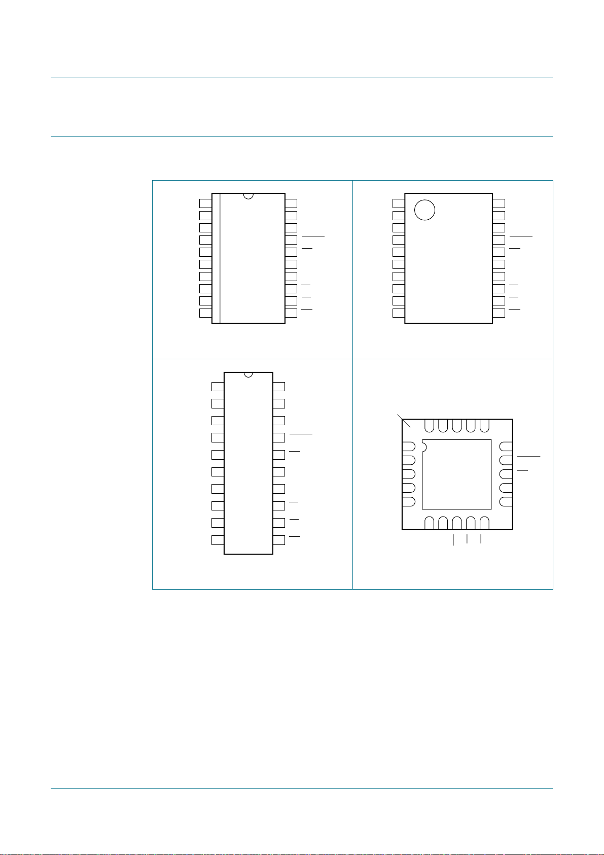
6. Pinning information
6.1 Pinning
PCA9665
Fm+ parallel bus to I2C-bus controller
1
D0
2
D1
3
D2
4
D3
5
D4
D5
D6
D7
i.c.
V
SS
6
7
8
9
10
PCA9665D
002aab020
20
19
18
17
16
15
14
13
12
11
V
DD
SDA
SCL
RESET
INT
A1
A0
CE
RD
WR
1
D0
2
D1
3
D2
4
D3
5
D4
D5
D6
D7
i.c.
V
SS
6
7
8
9
10
PCA9665PW
002aab021
20
19
18
17
16
15
14
13
12
11
V
SDA
SCL
RESET
INT
A1
A0
CE
RD
WR
Fig 2. Pin configuration of SO20 Fig 3. Pin configuration of TSSOP20
1
D0 V
2
D1 SDA
3
D2 SCL
4
D3 RESET
5
D4 INT
PCA9665N
6
D5 A1
7
D6 A0
8
D7 CE
9
i.c. RD
10
V
SS
002aab019
20
DD
19
18
17
16
15
14
13
12
11
WR
terminal 1
index area
D3 SCL
D4 RESET
D5 INT
D6
D7
D2D1D0
2019181716
1 15
2 14
3 13
PCA9665BS
4 12
5 11
6
i.c.
Transparent top view
DD
SDA
V
7
8
9
10
SS
RD
WR
V
CE
002aab022
DD
A1
A0
Fig 4. Pin configuration of DIP20 Fig 5. Pin configuration of HVQFN20
PCA9665_2 © NXP B.V. 2006. All rights reserved.
Product data sheet Rev. 02 — 7 December 2006 4 of 91
Page 5

NXP Semiconductors
6.2 Pin description
Table 2. Pin description
Symbol Pin Type Description
D0 1 18 I/O Data bus: Bidirectional 3-state data bus used to
D1 2 19 I/O
D2 3 20 I/O
D3 4 1 I/O
D4 5 2 I/O
D5 6 3 I/O
D6 7 4 I/O
D7 8 5 I/O
i.c. 9 6 - internally connected: must be left floating (pulled
V
SS
WR 11 8 I Write strobe: When LOW and CE is also LOW, the
RD 12 9 I Read strobe: When LOW and CE is also LOW,
CE 13 10 I Chip Enable: Active LOW input signal. When LOW,
A0 14 11 I Address inputs: Selects the bus controller’s internal
A1 15 12 I
INT 16 13 O Interrupt request: Active LOW, open-drain, output.
RESET 17 14 I Reset: Active LOW input. A LOWlevelclearsinternal
SCL 18 15 I/O I
SDA 19 16 I/O I
V
DD
[1] HVQFN package die supply ground is connected to both the VSSpin and the exposed center pad. The V
PCA9665
Fm+ parallel bus to I2C-bus controller
DIP20,
SO20,
TSSOP20
10 7
20 17 power Power supply: 2.3 V to 3.6 V
pin must be connected to supply ground for proper device operation. For enhanced thermal, electrical, and
board-level performance, the exposed pad needs to be soldered to the board using a corresponding
thermal pad on the board, and for proper heat conduction through the board thermal vias need to be
incorporated in the PCB in the thermal pad region.
HVQFN20
[1]
transfercommands, data and status between the bus
controller and the CPU. D0 is the least significant bit.
LOW internally)
power Supply ground
content of the data bus is loaded into the addressed
register. Data are latched on the rising edge of either
WR or CE.
causes the contents of the addressed register to be
presented on the data bus. The read cycle begins on
the falling edge of
data transfers between the CPU and the bus
controller are enabled on D0 to D7 as controlled by
the
WR, RD and A0 to A1 inputs. When HIGH,
places the D0 to D7 lines in the 3-state condition.
Data are written into the addressed register on rising
edge of either CE or WR.
registers and ports for read/write operations.
This pin requires a pull-up device.
registers and resets the I
2
C-bus serial clock input/output (open-drain).
This pin requires a pull-up device.
2
C-busserial data input/output (open-drain). This pin
requires a pull-up device.
RD.
2
C-bus state machine.
SS
PCA9665_2 © NXP B.V. 2006. All rights reserved.
Product data sheet Rev. 02 — 7 December 2006 5 of 91
Page 6

NXP Semiconductors
7. Functional description
7.1 General
The PCA9665 acts as an interface device between standard high-speed parallel buses
and the serial I2C-bus. On the I2C-bus, it can act either as a master or slave. Bidirectional
data transfer between the I2C-bus and the parallel-bus microcontroller is carried out on a
byte or buffered basis, using either an interrupt or polled handshake.
7.2 Internal oscillator
The PCA9665 contains an internal 28.5 MHz oscillator which is used for all I2C-bus timing.
The oscillator requires up to 550 µs to start-up after ENSIO bit is set to ‘1’.
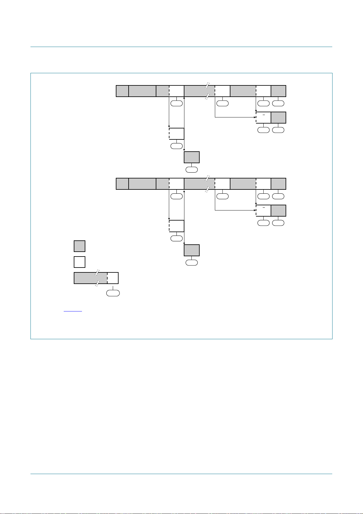
7.3 Registers
The PCA9665 contains eleven registers which are used to configure the operation of the
device as well as to send and receive serial data. There are four registers that can be
accessed directly and seven registers that are accessed indirectly by setting a register
pointer.
PCA9665
Fm+ parallel bus to I2C-bus controller
The four direct registers are selected by setting pins A0 and A1 to the appropriate logic
levels before a read or write operation is executed on the parallel bus.
The seven indirect registers require that the INDPTR (indirect register pointer, one of the
four direct registers described above) is initially loaded with the address of the register in
the indirect address space before a read or write is performed to the INDIRECT data field.
For example, in order to write to the indirectly addressed I2CSCLL register, the INDPTR
register should be loaded with 02h by performing a write to the direct INDPTR register
(A1 = 0, A0 = 0). Then the I2CSCLL register can be programmed by writing to the
INDIRECT data field (A1 = 1, A0 = 0) in the direct address space. Register mapping is
described in Table 3, Table 4 and Figure 6.
Remark: Do not write to any I2C-bus registers while the I2C-bus is busy and the PCA9665
is in master or addressed slave mode.
Table 3. Direct register selection by setting A0 and A1
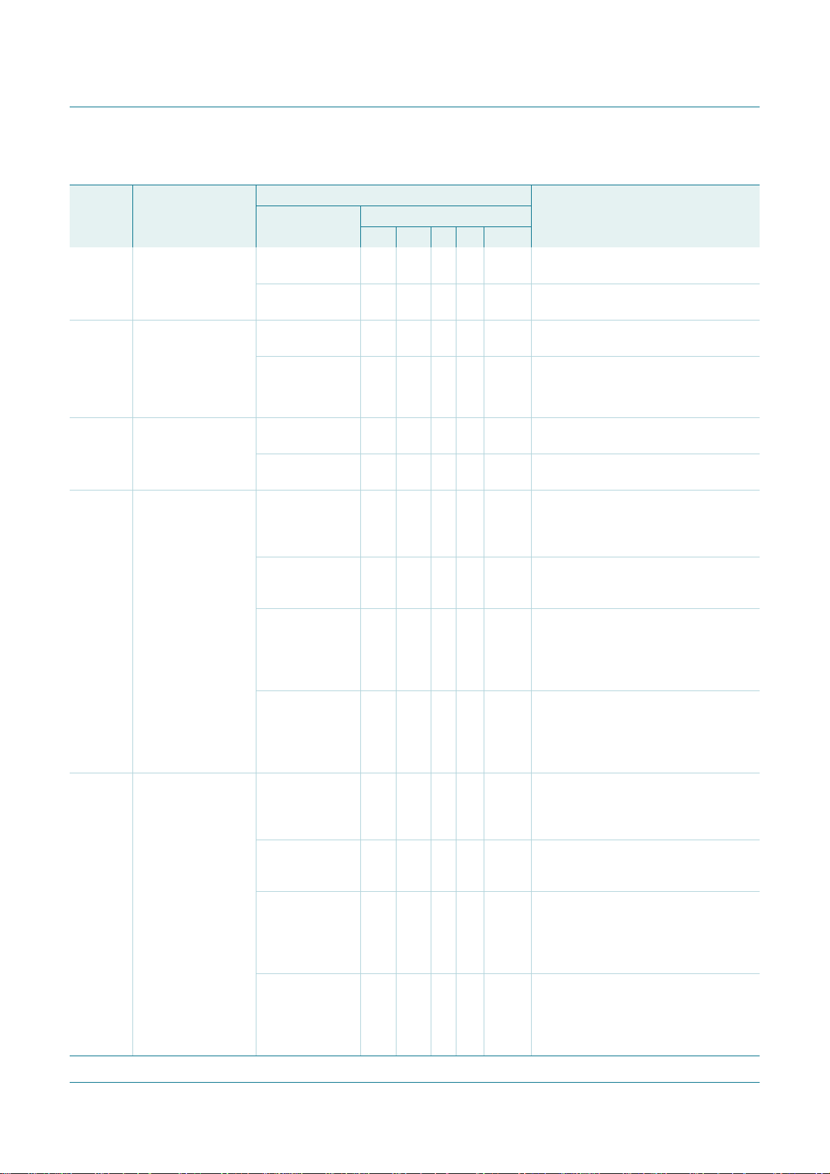
Register name Register function A1 A0 Read/Write Default
I2CSTA status 0 0 R F8h
INDPTR indirect register pointer 0 0 W 00h
I2CDAT data 0 1 R/W 00h
I2CCON control 1 1 R/W 00h
INDIRECT indirect data field
access
1 0 R/W 00h
[1]
[1] See Section 8.10 “Power-on reset” for more detail.
PCA9665_2 © NXP B.V. 2006. All rights reserved.
Product data sheet Rev. 02 — 7 December 2006 6 of 91
Page 7
NXP Semiconductors
Table 4. Indirect register selection by setting A1 = 1 and A0 = 0
Register name Register function INDPTR Read/Write Default
I2CCOUNT byte count 00h R/W 01h
I2CADR own address 01h R/W E0h
I2CSCLL SCL LOW period 02h R/W 9Dh
I2CSCLH SCL HIGH period 03h R/W 86h
I2CTO time-out 04h R/W FFh
I2CPRESET parallel software reset 05h W 00h
I2CMODE I
PCA9665
Fm+ parallel bus to I2C-bus controller
2
C-bus mode 06h R/W 00h
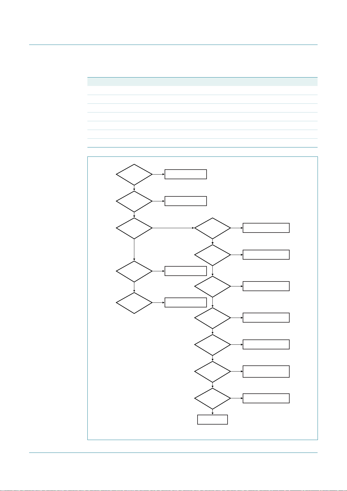
A1 A0 = 00
read?
no
A1 A0 = 00
write?
no
A1 A0 = 10
read/write?
no
A1 A0 = 01
read/write?
no
A1 A0 = 11
read/write?
yes
I2CSTA REGISTER
yes
INDPTR REGISTER
yes
yes
I2CDAT REGISTER
yes
I2CCON REGISTER
INDPTR = 00h
?
no
INDPTR = 01h
?
no
INDPTR = 02h
?
no
INDPTR = 03h
?
no
yes
I2CCOUNT REGISTER
yes
I2CADR REGISTER
yes
I2CSCLL REGISTER
yes
I2CSCLH REGISTER
INDPTR = 04h
?
no
INDPTR = 05h
?
no
INDPTR = 06h
?
no
RESERVED
yes
yes
yes
I2CTO REGISTER
I2CPRESET REGISTER
(write only)
I2CMODE REGISTER
002aab459
Fig 6. Register mapping flowchart
PCA9665_2 © NXP B.V. 2006. All rights reserved.
Product data sheet Rev. 02 — 7 December 2006 7 of 91
Page 8

NXP Semiconductors
7.3.1 Direct registers
7.3.1.1 The Status register, I2CSTA (A1 = 0, A0 = 0)
I2CSTA is an 8-bit read-only register. The two least significant bits are always zero. The
six most significant bits contain the status code. There are 30 possible status codes.
When I2CSTA contains F8h, it indicates the idle state and therefore no serial interrupt is
requested. All other I2CSTA values correspond to defined states. When each of these
states is entered, a serial interrupt is requested (SI = 1 and INT asserted LOW).
Remark: Data in I2CSTA is valid only when a serial interrupt occurs (SI = 1 and INT
asserted LOW). Reading the register when SI = 0 and INT is HIGH may cause wrong
values to be read.
Table 5. I2CSTA - Status register (A1 = 0, A0 = 0) bit allocation
Table 6. I2CSTA - Status register (A1 = 0, A0 = 0) bit description
Bit Symbol Description
7:2 ST[5:0] status code corresponding to the different I
1:0 - always at zero
PCA9665
Fm+ parallel bus to I2C-bus controller
7 6 5 4 3 2 1 0
ST5 ST4 ST3 ST2 ST1 ST0 0 0
2
C-bus states
7.3.1.2 The Indirect Pointer register, INDPTR (A1 = 0, A0 = 0)
Table 7. INDPTR - Indirect Register Pointer (A1 = 0, A0 = 0) bit allocation
7 6 5 4 3 2 1 0
- - - - - IP2 IP1 IP0
Table 8. INDPTR - Indirect Pointer register (A1 = 0, A0 = 0) bit description
Bit Symbol Description
7:3 - reserved; must be written with zeroes
2:0 IP2 to IP0 address of the indirect register
INDPTR is an 8-bit write-only register. It contains a pointer to a register in the indirect
address space (IP[2:0]). The value in the register will determine what indirect register will
be accessed when the INDIRECT register is read or written, as defined in Table 4.
7.3.1.3 The I2C-bus Data register, I2CDAT (A1 = 0, A0 = 1)
I2CDAT is an 8-bit read/write register. It contains a byte of serial data to be transmitted or
a byte which has just been received. In master mode, this includes the slave address that
the master wants to send out on the I2C-bus, with the most significant bit of the slave
address in the SD7 bit position and the Read/Write bit in the SD0 bit position. The CPU
can read from and write to this 8-bit register while the PCA9665 is not in the process of
shifting a byte. This occurs when PCA9665 is in a defined state and the serial interrupt
flag is set. Data in I2CDAT remains stable as long as SI is set. Whenever the PCA9665
generates an interrupt, the I2CDAT register contains the data byte that was just
transferred on the I2C-bus.
PCA9665_2 © NXP B.V. 2006. All rights reserved.
Product data sheet Rev. 02 — 7 December 2006 8 of 91
Page 9

NXP Semiconductors
In Byte mode, the CPU can read or write a single byte at a time. In Buffered mode, the
CPU can read or write up to 68 bytes at a time. See Section 8.1 “Configuration modes” for
more detail.
Remark: The I2CDAT register will capture the serial address as data when addressed via
the serial bus.
Remark: In Byte mode only, the data register will capture data from the serial bus during
38h (arbitration lost in slave address + R/W or data bytes causing this data in I2CDAT to
be changed), so the I2CDAT register will need to be reloaded when the bus becomes free.
In Buffered mode, the data is not written in the data register when arbitration is lost, which
keeps the buffer intact.
Table 9. I2CDAT - Data register (A1 = 0, A0 = 1) bit allocation
Table 10. I2CDAT - Data register (A1 = 0, A0 = 1) bit description
Bit Symbol Description
7:0 SD[7:0] Eight bits to be transmitted or just received. A logic 1 in I2CDAT corresponds to
PCA9665
Fm+ parallel bus to I2C-bus controller
7 6 5 4 3 2 1 0
SD7 SD6 SD5 SD4 SD3 SD2 SD1 SD0
2
a HIGH level on the I
C-bus. A logic 0 corresponds to a LOW level on the bus.
7.3.1.4 The Control register, I2CCON (A1 = 1, A0 = 1)
I2CCON is an 8-bit read/write register. Two bits are affected by the bus controller
hardware: the SI bit is set when a serial interrupt is requested, and the STO bit is cleared
when a STOP condition is present on the I2C-bus. A Write to the I2CCON register via the
parallel interface automatically clears the SI bit, which causes the Serial Interrupt line to
be de-asserted and the next clock pulse on the SCL line to be generated.
Remark: Since none of the registers should be written to via the parallel interface once
the Serial Interrupt line has been de-asserted, all the other registers that need to be
modified should be written to before the content of the I2CCON register is modified.
Table 11. I2CCON - Control register (A1 = 1, A0 = 1) bit allocation
7 6 5 4 3 2 1 0
AA ENSIO STA STO SI - - MODE
PCA9665_2 © NXP B.V. 2006. All rights reserved.
Product data sheet Rev. 02 — 7 December 2006 9 of 91
Page 10

NXP Semiconductors
Table 12. I2CCON - Control register (A1 = 1, A0 = 1) bit description
Bit Symbol Description
7 AA The Assert Acknowledge flag.
6 ENSIO The bus controller enable bit.
PCA9665
Fm+ parallel bus to I2C-bus controller
AA = 1: If the AA flag is set, an acknowledge (LOW level on SDA) will be returned
during the acknowledge clock pulse on the SCL line when:
• ‘Own slave address’ has been received (as defined in I2CADR register).
• A data byte has been received while the bus controller is in the Master
Receiver mode.
• A data byte has been received while the bus controller is in the addressed
Slave Receiver mode.
AA = 0: if the AA flag is reset, a not acknowledge (HIGH level on SDA) will be
returned during the acknowledge clock pulse on SCL when:
• ‘Own slave address’ has been received (as defined in I2CADR register).
• A data byte has been received while the PCA9665 is in the Master Receiver
mode.
• A data byte has been received while the PCA9665 is in the addressed Slave
Receiver mode.
When the bus controller is in the addressed Slave Transmitter mode, state C8h
will be entered after the last data byte is transmitted and an ACK is received from
the Master Receiver (see
PCA9665 enters the not addressed Slave Receiver mode, and the SDA line
remains at a HIGH level. In state C8h, the AA flag can be set again for future
address recognition.
When the PCA9665 is in the not addressed slave mode, its own slave address is
ignored. Consequently, no acknowledge is returned, and a serial interrupt is not
requested. Thus, the bus controller can be temporarily released from the I
while the bus status is monitored. While the bus controller is released from the
bus, START and STOP conditions are detected, and serial data is shifted in.
Address recognition can be resumed at any time by setting the AA flag.
ENSIO = 0: When ENSIO is ‘0’, the SDA and SCL outputs are in a
high-impedance state. SDAand SCL input signals are ignored, the PCA9665 is in
the ‘not addressed’ slave state. Internal oscillator is off.
ENSIO = 1: When ENSIO is ‘1’, the PCA9665 is enabled.
After the ENSIO bit is set to ‘1’, it takes 550 µs enable time for the internal
oscillator to start up and the serial interface to initialize. The PCA9665 will enter
either the master or the slave mode after this time. ENSIO should not be used to
temporarily release the PCA9665 from the I
2
the I
C-bus status is lost. The AA flag should be used instead (see description of
the AA flag above).
In the following text, it is assumed that ENSIO = ‘1’ for Normal mode operation.
For power-up behavior, please refer to
Figure 10 and Figure 14). When SI is cleared, the
2
C-bus since, when ENSIO is reset,
Section 8.10 “Power-on reset”.
2
C-bus
PCA9665_2 © NXP B.V. 2006. All rights reserved.
Product data sheet Rev. 02 — 7 December 2006 10 of 91
Page 11

NXP Semiconductors
PCA9665
Fm+ parallel bus to I2C-bus controller
Table 12. I2CCON - Control register (A1 = 1, A0 = 1) bit description
Bit Symbol Description
5 STA The START flag.
STA = 1: When the STA bit is set to enter a master mode, the bus controller
hardware checks the status of the I
bus is free. If the bus is not free, then the bus controller waits for a STOP condition
(which will free the bus) and generates a START condition after the minimum
buffer time (t
If STAis set while the bus controller is already in a master mode and one or more
bytes are transmitted or received, the bus controller transmits a repeated START
condition. STA may be set at any time. STA may also be set when the bus
controller is an addressed slave.A START condition will then be generated after a
STOP condition and the minimum buffer time (t
STA = 0: When the STA bit is reset, no START condition or repeated START
condition will be generated.
4 STO The STOP flag.
STO = 1: When the STO bit is set while the bus controller is in a master mode, a
STOPcondition is transmitted on the I
on the bus, the hardware clears the STO flag.
If the STA and STO bits are both set, then a STOP condition is transmitted on the
I2C-bus, if the PCA9665 is in a master mode. the bus controller then transmits a
START condition after the minimum buffer time (t
STO=0: When the STO bit is reset, no STOP condition will be generated.
3 SI The Serial Interrupt flag.
SI = 1: When the SI flag is set, and, if the ENSIO bit is also set, a serial interrupt is
requested. SI is set by hardware when one of 29 of the 30 possible states of the
bus controller states is entered. The only state that does not cause SI to be set is
state F8h, which indicates that no relevant state information is available.
While SI is set, the LOW period of the serial clock on the SCL line is stretched,
and the serial transfer is suspended. A HIGH level on the SCL line is unaffected
by the serial interrupt flag. SI is automatically cleared when the I2CCON register
is written. The SI bit cannot be set by the user.
SI = 0: When the SI flag is reset, no serial interrupt is requested, and there is no
stretching of the serial clock on the SCL line.
2:1 - Reserved. When I2CCON is read, zeroes are read. Must be written with zeroes.
0 MODE The Mode flag.
MODE = 0; Byte mode. See
MODE = 1; buffered mode. See
) has elapsed.
BUF
2
C-bus and generates a START condition if the
BUF
2
C-bus.When a STOP condition is detected
Section 8.1.1 “Byte mode” for more detail.
Section 8.1.2 “Buffered mode” for more detail.
…continued
) has elapsed.
) has elapsed.
BUF
Remark: ENSIO bit value must be changed only when the I2C-bus is idle.
7.3.1.5 The indirect data field access register, INDIRECT (A1 = 1, A0 = 0)
The registers in the indirect address space can be accessed using the INDIRECT data
field. Before writing or reading such a register, the INDPTR register should be written with
the address of the indirect register that needs to be accessed. Once the INDPTR register
contains the appropriate value, reads and writes to the INDIRECT data field will actually
read and write the selected indirect register.
PCA9665_2 © NXP B.V. 2006. All rights reserved.
Product data sheet Rev. 02 — 7 December 2006 11 of 91
Page 12

NXP Semiconductors
7.3.2 Indirect registers
7.3.2.1 The Byte Count register, I2CCOUNT (indirect address 00h)
The I2CCOUNT register is an 8-bit read/write register. It contains the number of bytes that
havebeen stored in Master/Slave Buffered Receiver mode, and the number of bytes to be
sent in Master/Slave Buffered Transmitter mode. Bit 7 is the last byte control bit and
applies to the Master/Slave Buffered Receiver mode only. The data in the I2CCOUNT
register is relevant only in Buffered mode (MODE = 1) and should not be used (read or
written) in Byte mode (MODE = 0).
Table 13. I2CCOUNT - Byte Count register (indirect address 00h) bit allocation
Table 14. I2CCOUNT - Byte Count register (indirect address 00h) bit description
Bit Symbol Description
7 LB Last Byte control bit. Master/Slave Buffered Receiver mode only.
6:0 BC[6:0] Number of bytes to be read or written (up to 68 bytes). If BC[6:0] is equal to 0 or
PCA9665
Fm+ parallel bus to I2C-bus controller
7 6 5 4 3 2 1 0
LB BC6 BC5 BC4 BC3 BC2 BC1 BC0
LB = 1: PCA9665 does not acknowledge the last received byte.
LB = 0: PCA9665 acknowledges the last received byte. A future bus
transaction must complete the read sequence by not acknowledging the last
byte.
greater than 68 (44h), no bytes will be read or written and an interrupt is
immediately generated after writing to the I2CCON register (in Buffered mode
only).
7.3.2.2 The Own Address register, I2CADR (indirect address 01h)
I2CADR is an 8-bit read/write register. It is not affected by the bus controller hardware.
The content of this register is irrelevant when the bus controller is in a master mode. In the
slavemodes, the sevenmost significant bits must be loaded with the microcontroller's own
slave address and the least significant bit determines if the General Call address will be
recognized or not.
Remark: AD[7:1] must be different from the General Call address (000 0000) for proper
device operation.
Table 15. I2CADR - Address register (indirect address 01h) bit allocation
7 6 5 4 3 2 1 0
AD7 AD6 AD5 AD4 AD3 AD2 AD1 GC
Table 16. I2CADR - Address register (indirect address 01h) bit description
Bit Symbol Description
7:1 AD[7:1] Own slave address. The most significant bit corresponds to the first bit received
from the I
HIGH level on the I
0 GC General Call.
2
C-bus after a START condition. A logic 1 in I2CADR corresponds to a
GC = 1: General Call address (00h) is recognized.
GC = 0: General Call address (00h) is ignored.
2
C-bus, and a logic 0 corresponds to a LOW level on the bus.
PCA9665_2 © NXP B.V. 2006. All rights reserved.
Product data sheet Rev. 02 — 7 December 2006 12 of 91
Page 13

NXP Semiconductors
7.3.2.3 The Clock Rate registers, I2CSCLL and I2CSCLH (indirect addresses 02h and 03h)
I2CSCLL and I2CSCLH are 8-bit read/write registers. They define the data rate for the
PCA9665 when used as a bus master. The actual frequency is determined by t
where SCL is HIGH), t
t
HIGH
and I2CSCLL registers and the internal oscillator frequency. tr and tf are
system/application dependent.
and t
PCA9665
Fm+ parallel bus to I2C-bus controller
(time where SCL is LOW), tr(rise time), and tf(fall time) values.
LOW
are calculated based on the values that are programmed into I2CSCLH
LOW
HIGH
(time
f
SCL
with T
=
---------------------------------------------------------------------------------------------- -
T
I2CSCLL I2CSCLH+()trt
osc
= internal oscillator period = 35 ns ± 5ns
osc
1
++
f
Remark: The I2CMODE register needs to be programmed before programming the
I2CSCLL and I2CSCLH registers in order to know which I2C-bus mode is selected. See
Section 7.3.2.6 “The I2C-bus mode register, I2CMODE (indirect address 06h)” for more
detail.
Standard-mode is the default selected mode at power-up or after reset.
Table 17. I2CSCLL - Clock Rate Low register (indirect address 02h) bit allocation
7 6 5 4 3 2 1 0
L7 L6 L5 L4 L3 L2 L1 L0
Table 18. I2CSCLL - Clock Rate Low register (indirect address 02h) bit description
Bit Symbol Description
7:0 L[7:0] Eight bits defining the LOW state of SCL.
Table 19. I2CSCLH - Clock Rate High register (indirect address 03h) bit allocation
7 6 5 4 3 2 1 0
H7 H6 H5 H4 H3 H2 H1 H0
Table 20. I2CSCLH - Clock Rate High register (indirect address 03h) bit description
Bit Symbol Description
7:0 H[7:0] Eight bits defining the HIGH state of SCL.
PCA9665_2 © NXP B.V. 2006. All rights reserved.
Product data sheet Rev. 02 — 7 December 2006 13 of 91
Page 14

NXP Semiconductors
7.3.2.4 The Time-out register, I2CTO (indirect address 04h)
I2CTOis an 8-bit read/write register. It is used to determine the maximum time that SCL is
allowed to be in a LOW logic state before the I2C-bus state machine is reset or the
PCA9665 initiates a forced action on the I2C-bus.
When the I2C-bus interface is operating, I2CTO is loaded in the time-out counter at every
LOW SCL transition.
Table 21. I2CTO - Time-out register (indirect register 04h) bit allocation
Table 22. I2CTO - Time-out register (indirect register 04h) bit description
Bit Symbol Description
7 TE Time-out enable/disable
6:0 TO[6:0] Time-out value. The time-out period = (I2CTO[6:0] + 1) × 143.36 µs.
PCA9665
Fm+ parallel bus to I2C-bus controller
7 6 5 4 3 2 1 0
TE TO6 TO5 TO4 TO3 TO2 TO1 TO0
TE = 1: Time-out function enabled
TE = 0: Time-out function disabled
The time-out value may vary some, and is an approximate value.
The Time-out register can be used in the following cases:
• When the bus controller, in the master mode, wants to send a START condition and
the SCL line is held LOW by some other device. Then the bus controller waits a time
period equivalent to the time-out value for the SCL to be released. In case it is not
released, the bus controller concludes that there is a bus error, loads 78h in the
I2CSTA register, generates an interrupt signal and releases the SCL and SDA lines.
After the microcontroller reads the status register, it needs to send a reset in order to
reset the bus controller.
• In the master mode, the time-out feature starts every time the SCL goes LOW. If SCL
stays LOW for a time period equal to or greater than the time-out value, the bus
controller concludes there is a bus error and behaves in the manner described above.
When the I2C-bus interface is operating, I2CTO is loaded in the time-out counter at
every SCL transition. See Section 8.11 “Reset” for more information.
• In case of a forced access to the I
access to the I2C-bus”.)
7.3.2.5 The Parallel Software Reset register, I2CPRESET (indirect address 05h)
I2CPRESET is an 8-bit write-only register. Programming the I2CPRESET register allows
the user to reset the PCA9665 under software control. The software reset is achieved by
writing two consecutive bytes to this register. The first byte must be A5h while the second
byte must be 5Ah. The writes must be consecutive and the values must match A5h and
5Ah. If this sequence is not followed as described, the reset is aborted.
2
C-bus. (See more details in Section 8.9.3 “Forced
PCA9665_2 © NXP B.V. 2006. All rights reserved.
Product data sheet Rev. 02 — 7 December 2006 14 of 91
Page 15

NXP Semiconductors
7.3.2.6 The I2C-bus mode register, I2CMODE (indirect address 06h)
I2CMODE is an 8-bit read/write register. It contains the control bits that select the correct
timing parameters when the device is used in master mode (AC[1:0]). Timing parameters
involved with AC[1:0] are t
Table 23. I2CMODE - I2C-bus Mode register (indirect address 06h) bit allocation
Table 24. I2CMODE - I
Bit Symbol Description
7:2 - Reserved. When I2CMODE is read, zeroes are read. Must be written
1:0 AC[1:0] I
PCA9665
Fm+ parallel bus to I2C-bus controller
, t
BUF
7 6 5 4 3 2 1 0
------AC1AC0
2
C-bus Mode register (indirect address 06h) bit description
with zeroes.
2
C-bus mode selection to ensure proper timing parameters (see
Table 25).
AC[1:0] = 00: Standard-mode AC parameters selected.
AC[1:0] = 01: Fast-mode AC parameters selected.
AC[1:0] = 10: Fast-mode Plus AC parameters selected.
AC[1:0] = 11: Turbo mode. In this mode, the user is not limited to a
maximum frequency of 1 MHz.
HD;STA
, t
SU;STA
, t
SU;STO
, t
HIGH
, t
LOW
.
Remark: Change from an I2C-bus mode to a slower one (Fast-mode to Standard-mode,
for example) will cause the HIGH and LOW timings of SCL to be violated. It is then
required to program the I2CSCLL and I2CSCLH registers with values in accordance with
the selected mode.
2
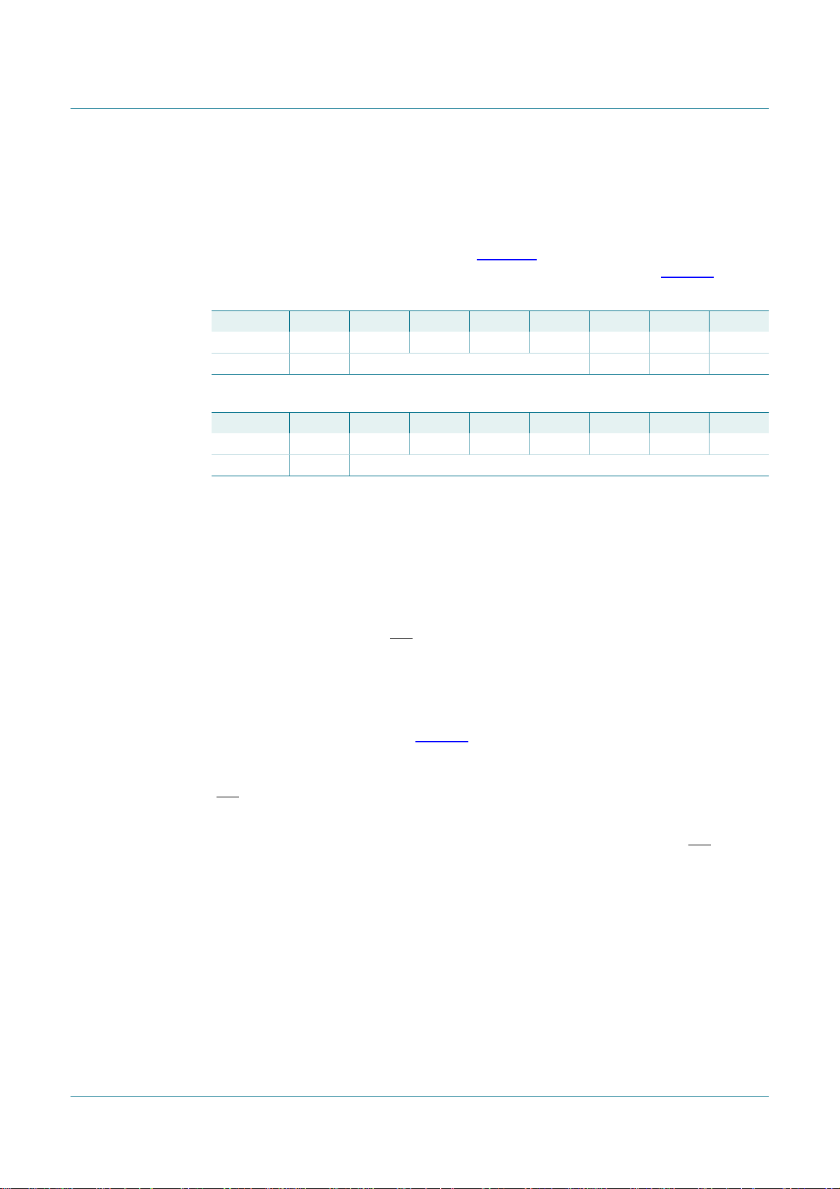
Table 25. I
I2CSCLL
(hexadecimal)
9D 86 99.9 00 Standard
2C 14 396.8 01 Fast
11 09 952.3 10 Fast-mode Plus
0E 05 11 Turbo mode
[1] I2CSCLL and I2CSCLH values in the table also represents the minimum values that can be used for the
corresponding I2C-bus mode. Use of lower values will cause the minimum values to be loaded.
[2] Using the formula
C-bus mode selection example
I2CSCLH
(hexadecimal)
f
=
---------------------------------------------------------------------------------------------- -
SCL
T
I2CSCLL I2CSCLH+()trt
osc
[1]
I2C-bus frequency
[2]
(kHz)
1
AC[1:0] Mode
++
f
PCA9665_2 © NXP B.V. 2006. All rights reserved.
Product data sheet Rev. 02 — 7 December 2006 15 of 91
Page 16

NXP Semiconductors
8. PCA9665 modes
8.1 Configuration modes
Byte mode and Buffered mode are selected using the MODE bit in I2CCON register:
MODE = 0: Byte mode
MODE = 1: Buffered mode
8.1.1 Byte mode
The Byte mode allows communication on a single command basis. Only one specific
command is executed at a time and the Status Register is updated once this single
command has been performed. A command can be a START, a STOP, a Byte Write, a
Byte Read, and so on.
8.1.2 Buffered mode
The Buffered mode allows several instructions to be executed before an Interrupt is
generated and before the I2CSTA register is updated. This allows the microcontroller to
request a sequence, up to 68 bytes in a single transmission and lets the PCA9665
perform it without having to access the Status Register and the Control Register each time
a single command is performed. The microcontroller can then perform other tasks while
the PCA9665 performs the requested sequence.
PCA9665
Fm+ parallel bus to I2C-bus controller
The number of bytes that needs to be sent from the internal buffer (Transmitter mode) or
received into the internal buffer (Receiver mode) is defined in the indirectly addressed
I2CCOUNT Register (BC[6:0]). Up to 68 bytes can be sent or received.
8.2 Operating modes
The four operating modes are:
• Master Transmitter
• Master Receiver
• Slave Receiver
• Slave Transmitter
Each mode can be used on a byte basis (Byte mode) or in an up to 68-byte buffer basis
(Buffered mode).
Data transfers in each mode of operation are shown in Figure 7 through Figure 10. These
figures contain the following abbreviations:
S — START condition
SLA — 7-bit slave address
R — Read bit (HIGH level at SDA)
W — Write bit (LOW level at SDA)
A — Acknowledge bit (LOW level at SDA)
A — Not acknowledge bit (HIGH level at SDA)
Data — 8-bit data byte
PCA9665_2 © NXP B.V. 2006. All rights reserved.
Product data sheet Rev. 02 — 7 December 2006 16 of 91
Page 17

NXP Semiconductors
P — STOP condition
In Figure 7, Figure 8, Figure 9, Figure 10, Figure 11, Figure 12, Figure 13 and Figure 14,
circles are used to indicate when the serial interrupt flag is set. A serial interrupt is not
generated when I2CSTA = F8h. This happens on a STOP condition or when an external
reset is generated (at power-up, when RESET pin is going LOW or during a software reset
on the parallel bus). The numbers in the circles show the status code held in the I2CSTA
register. At these points, a service routine must be executed to continue or complete the
serial transfer. These service routines are not critical since the serial transfer is
suspended until the serial interrupt flag is cleared by software.
When a serial interrupt routine is entered, the status code in I2CSTA is used to branch to
the appropriate service routine. For each status code, the required software action and
details of the following serial transfer are given in Table 27, Table 28, Table 31, Table 32,
Table 35, Table 36, Table 40, and Table 41.
8.3 Byte mode
8.3.1 Master Transmitter Byte mode
PCA9665
Fm+ parallel bus to I2C-bus controller
In the Master Transmitter Byte mode, a number of data bytes are transmitted to a slave
receiver (see Figure 7). Before the Master Transmitter Byte mode can be entered,
I2CCON must be initialized as shown in Table 26.
Table 26. I2CCON initialization (Byte mode)
Bit 7 6 5 4 3 2 1 0
Symbol AA ENSIO STA STO SI reserved reserved MODE
Value X1000XX0
ENSIO must be set to logic 1 to enable the PCA9665. If the AA bit is reset, the PCA9665
will not acknowledge its own slave address in the event of another device becoming
master of the bus. (In other words, if AA is reset, PCA9665 cannot enter a slave mode.)
STA, STO,and SI must be reset. Once ENSIO has been set to 1, it takes about 550 µsfor
the oscillator to start up.
The Master Transmitter Byte mode may now be entered by setting the STA bit. The
I2C-bus state machine will first test the I2C-bus and generate a START condition as soon
as the bus becomes free. When a START condition is transmitted, the serial interrupt flag
(SI) is set, the Interrupt line (INT) goes LOW and the status code in the status register
(I2CSTA) will be 08h. This status code must be used to vector to an interrupt service
routine that loads I2CDAT with the slave address and the data direction bit (SLA+W). A
write to I2CCON resets the SI bit, clears the Interrupt (INT goes HIGH) and allows the
serial transfer to continue.
When the slave address with the direction bit have been transmitted, the Serial Interrupt
flag (SI) is set again, the Interrupt line (INT) goes LOW again and I2CSTA is loaded with
the following possible codes:
• 18h if an acknowledgment bit (ACK) has been received
• 20h if an no acknowledgment bit (NACK) has been received
• 38h if the PCA9665 lost the arbitration
PCA9665_2 © NXP B.V. 2006. All rights reserved.
Product data sheet Rev. 02 — 7 December 2006 17 of 91
Page 18

NXP Semiconductors
• B0h if the PCA9665 lost the arbitration and is addressed as a slave transmitter (slave
• 68h if the PCA9665 lost the arbitration and is addressed as a slave receiver (slave
• D8h if the PCA9665 lost the arbitration and is addressed as a slave receiver during a
The appropriate action to be taken for each of these status codes is detailed in Table 27.
ENSIO is not affected by the serial transfer and is not referred to in Table 27.
After a repeated START condition (state 10h), the PCA9665 may switch to the Master
Receiver mode by loading I2CDAT with SLA+R.
Remark: A master should not transmit its own slave address.
PCA9665
Fm+ parallel bus to I2C-bus controller
mode enabled with AA = 1)
mode enabled with AA = 1)
General Call sequence (slave mode enabled with AA = 1 and General Call address
enabled with GC = 1 in I2CADR register)
PCA9665_2 © NXP B.V. 2006. All rights reserved.
Product data sheet Rev. 02 — 7 December 2006 18 of 91
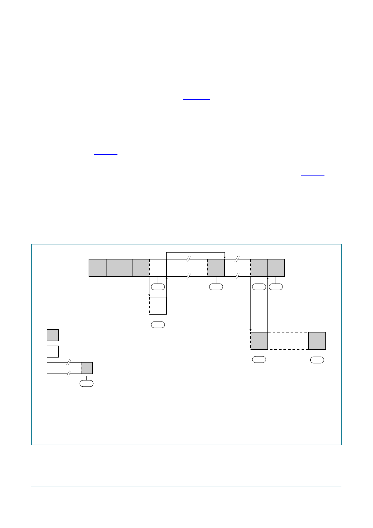
Page 19
NXP Semiconductors
PCA9665
Fm+ parallel bus to I2C-bus controller
MT
successful
transmission
to a Slave Receiver
next transfer started with a
repeated START condition
Not Acknowledge received after
the slave address
Not Acknowledge received after
a data byte
arbitration lost in slave address
or data byte
S SLA W A
08h
18h
A P
20h F8h
A or A
38h
other MST
continues
DATA
A P
28h F8h
(2)
A P
30h F8h
(3)
A or A
38h
S SLA W
10h
to Master Receiver
mode entry = MR
other MST
continues
R
(4)
other MST
arbitration lost and addressed as slave
from master to slave
from slave to master
any number of data bytes and
DATA
A
their associated Acknowledge bits
This number (contained in I2CSTA) corresponds
n
to a defined state of the I
A
B0h
68h
D8h
2
C-bus.
continues
to corresponding states in Slave Transmitter mode
to corresponding states in Slave Receiver mode
to corresponding states in Slave Receiver mode (General Call)
(1)
(1) See Table 27
(2) Defined state when a single byte is sent and an ACK is received.
(3) Defined state when a single byte is sent and a NACK is received.
(4) Master Receiver Byte mode is entered when MODE = 0. Master Receiver Buffered mode is entered when MODE = 1.
Fig 7. Format and states in the Master Transmitter Byte mode (MODE = 0)
002aab024
PCA9665_2 © NXP B.V. 2006. All rights reserved.
Product data sheet Rev. 02 — 7 December 2006 19 of 91
Page 20

NXP Semiconductors
Table 27. Master Transmitter Byte mode (MODE = 0)
Status
code
(I2CSTA)
08h A START condition
10h A repeated START
18h SLA+W has been
20h SLA+W has been
Status of the
2
I
C-bus and the
PCA9665
has been transmitted
condition has been
transmitted
transmitted; ACK has
been received
transmitted; NACK
has been received
Application software response Next action taken by the PCA9665
To/from I2CDAT To I2CCON
STA STO SI AA MODE
Load SLA+W X X 0 X 0 SLA+W will be transmitted;
Load SLA+W or X X 0 X 0 SLA+W will be transmitted;
Load SLA+R X X 0 X 0 SLA+R will be transmitted;
Load data byte or 0 0 0 X 0 Data byte will be transmitted;
noI2CDATactionor1 0 0 X 0 Repeated START will be transmitted;
noI2CDATactionor0 1 0 X 0 STOP condition will be transmitted;
no I2CDAT action 1 1 0 X 0 STOPconditionfollowedby a START
Load data byte or 0 0 0 X 0 Data byte will be transmitted;
noI2CDATactionor1 0 0 X 0 Repeated START will be transmitted;
PCA9665
Fm+ parallel bus to I2C-bus controller
ACK/NACK will be received
ACK/NACK will be received
PCA9665 will be switched to Master
Receiver Byte mode
ACK/NACK will be received
STO flag will be reset
condition will be transmitted;
STO flag will be reset
ACK/NACK will be received
28h Data byte in I2CDAT
has been transmitted;
ACK has been
received
noI2CDATactionor0 1 0 X 0 STOP condition will be transmitted;
STO flag will be reset
no I2CDAT action 1 1 0 X 0 STOPconditionfollowedby a START
condition will be transmitted;
STO flag will be reset
Load data byte or 0 0 0 X 0 Data byte will be transmitted;
ACK/NACK will be received
noI2CDATactionor1 0 0 X 0 Repeated START will be transmitted;
noI2CDATactionor0 1 0 X 0 STOP condition will be transmitted;
STO flag will be reset
no I2CDAT action 1 1 0 X 0 STOPconditionfollowedby a START
condition will be transmitted;
STO flag will be reset
PCA9665_2 © NXP B.V. 2006. All rights reserved.
Product data sheet Rev. 02 — 7 December 2006 20 of 91
Page 21

NXP Semiconductors
PCA9665
Fm+ parallel bus to I2C-bus controller
Table 27. Master Transmitter Byte mode (MODE = 0)
Status
code
(I2CSTA)
30h Data byte in I2CDAT
38h Arbitration lost in
Status of the
2
I
C-bus and the
PCA9665
has been transmitted;
NACK has been
received
SLA+W or Data bytes
Application software response Next action taken by the PCA9665
To/from I2CDAT To I2CCON
STA STO SI AA MODE
Load data byte or 0 0 0 X 0 Data byte will be transmitted;
noI2CDATactionor1 0 0 X 0 Repeated START will be transmitted;
noI2CDATactionor0 1 0 X 0 STOP condition will be transmitted;
no I2CDAT action 1 1 0 X 0 STOPconditionfollowedby a START
No I2CDAT
action or
No I2CDAT
action or
No I2CDAT
action
00000 I
00010 I
1 0 0 X 0 A START condition will be
…continued
ACK/NACK will be received
STO flag will be reset
condition will be transmitted;
STO flag will be reset
2
C-bus will be released;
PCA9665 will enter Slave mode.
2
C-bus will be released;
PCA9665 will enter the Slave mode.
transmitted when the bus becomes
free
PCA9665_2 © NXP B.V. 2006. All rights reserved.
Product data sheet Rev. 02 — 7 December 2006 21 of 91
Page 22

NXP Semiconductors
8.3.2 Master Receiver Byte mode
In the Master Receiver Byte mode, a number of data bytes are received from a slave
transmitter one byte at a time (see Figure 8). The transfer is initialized as in the Master
Transmitter Byte mode.
The Master Receiver Byte mode may now be entered by setting the STA bit. The I2C-bus
state machine will first test the I2C-bus and generate a START condition as soon as the
bus becomes free. When a START condition is transmitted, the Serial Interrupt flag (SI) is
set, the Interrupt line (INT) goes LOW and the status code in the status register (I2CSTA)
will be 08h. This status code must be used to vector to an interrupt service routine that
loads I2CDAT with the slave address and the data direction bit (SLA+R). A write to
I2CCON resets the SI bit, clears the Interrupt (INT goes HIGH) and allows the serial
transfer to continue.
When the slave address and the data direction bit have been transmitted, the serial
interrupt flag (SI) is set again, the Interrupt line (INT) goes LOW again and I2CSTA is
loaded with the following possible codes:
• 40h if an acknowledgment bit (ACK) has been received for the slave address with
• 48h if a no acknowledgment bit (NACK) has been received for the slave address with
• 38h if the PCA9665 lost the arbitration
• B0h if the PCA9665 lost the arbitration and is addressed as a slave transmitter (slave
• 68h if the PCA9665 lost the arbitration and is addressed as a slave receiver (slave
• D8h if the PCA9665 lost the arbitration and is addressed as a slave receiver during a
PCA9665
Fm+ parallel bus to I2C-bus controller
direction bit
direction bit
mode enabled with AA = 1)
mode enabled with AA = 1)
General Call sequence (slave mode enabled with AA = 1 and General Call address
enabled with GC = 1 in I2CADR register).
The appropriate action to be taken for each of these status codes is detailed in Table 28.
ENSIO is not affected by the serial transfer and is not referred to in Table 28.
After a repeated START condition (state 10h), the PCA9665 may switch to the Master
Transmitter mode by loading I2CDAT with SLA+W.
Remark: A master should not transmit its own slave address.
PCA9665_2 © NXP B.V. 2006. All rights reserved.
Product data sheet Rev. 02 — 7 December 2006 22 of 91
Page 23
NXP Semiconductors
PCA9665
Fm+ parallel bus to I2C-bus controller
MR
successful
reception from
a Slave Transmitter
next transfer started with a
repeated START condition
Not Acknowledge received after
the slave address
arbitration lost in slave address
or Acknowledge bit
arbitration lost and addressed as slave
S SLA R A
08h
40h
A P
48h F8h
A or A
38h
A
DATA
other MST
continues
other MST
continues
A P
DATA A
50h F8h
(2) (3)
58h
10h
to Master Transmitter mode
other MST
A
continues
38h
S SLA R
entry = MT
W
(4)
to corresponding states in Slave Transmitter mode
to corresponding states in Slave Receiver mode
to corresponding states in Slave Receiver mode (General Call)
(1)
from master to slave
from slave to master
DATA
B0h
68h
D8h
any number of data bytes and
A
their associated Acknowledge bits
This number (contained in I2CSTA) corresponds
n
to a defined state of the I
2
C-bus.
(1) See Table 28.
(2) Defined state when a single byte is received and an ACK is sent (AA = 1).
(3) Defined state when a single byte is received and a NACK is sent (AA = 0).
(4) Master Transmitter Byte mode is entered when MODE = 0. Master Transmitter Buffered mode is entered when MODE = 1.
Fig 8. Format and states in the Master Receiver Byte mode (MODE = 0)
002aab025
PCA9665_2 © NXP B.V. 2006. All rights reserved.
Product data sheet Rev. 02 — 7 December 2006 23 of 91
Page 24

NXP Semiconductors
Table 28. Master Receiver Byte mode (MODE = 0)
Status
code
(I2CSTA)
08h A START condition
10h A repeated START
38h Arbitration lost in
40h SLA+R has been
48h SLA+R has been
50h Data byte has been
58h Data byte has been
Status of the
2
I
C-bus and the
PCA9665
has been
transmitted
condition has been
transmitted
NACK bit
transmitted; ACK
has been received
transmitted; NACK
has been received
received; ACK has
been returned
received; NACK has
been returned
Application software response Next action taken by the PCA9665
To/from I2CDAT To I2CCON
Load SLA+R X X 0 X 0 SLA+R will be transmitted;
Load SLA+R or X X 0 X 0 SLA+R will be transmitted;
Load SLA+W X X 0 X 0 SLA+W will be transmitted;
No I2CDAT actionor000X0 I
no I2CDAT action 1 0 0 X 0 A START condition will be
No I2CDAT actionor0 0 0 0 0 Data byte will be received;
no I2CDAT action 0 0 0 1 0 Data byte will be received;
No I2CDAT actionor1 0 0 X 0 Repeated START condition will be
no I2CDAT actionor0 1 0 X 0 STOP condition will be transmitted;
no I2CDAT action 1 1 0 X 0 STOPconditionfollowedby a START
Read data byte or 0 0 0 0 0 Data byte will be received;
read data byte 0 0 0 1 0 Data byte will be received;
Read data byte or 1 0 0 X 0 Repeated START condition will be
read data byte or 0 1 0 X 0 STOP condition will be transmitted;
read data byte 1 1 0 X 0 STOPcondition followed byaSTART
Fm+ parallel bus to I2C-bus controller
STA STO SI AA MODE
PCA9665
ACK/NACK bit will be received
ACK/NACK bit will be received
PCA9665 will be switched to
Master Transmitter Byte mode
2
C-bus will be released;
PCA9665 will enter a slave mode
transmitted when the bus becomes
free
NACK bit will be returned
ACK bit will be returned
transmitted
STO flag will be reset
condition will be transmitted;
STO flag will be reset
NACK bit will be returned
ACK bit will be returned
transmitted
STO flag will be reset
condition will be transmitted;
STO flag will be reset
PCA9665_2 © NXP B.V. 2006. All rights reserved.
Product data sheet Rev. 02 — 7 December 2006 24 of 91
Page 25
NXP Semiconductors
8.3.3 Slave Receiver Byte mode
In the Slave Receiver Byte mode, a number of data bytes are received from a master
transmitter one byte at a time (see Figure 9). To initiate the Slave Receiver mode, I2CADR
and I2CCON must be loaded as shown in Table 29 and Table 30.
Table 29. I2CADR initialization
Bit 7 6 5 4 3 2 1 0
Symbol AD7 AD6 AD5 AD4 AD3 AD2 AD1 GC
Value own slave address X
The upper 7 bits are the I2C-bus address to which PCA9665 will respond when addressed
by a master. GC is the control bit that allows the PCA9665 to respond or not to the
General Call address (00h).
When programmed to logic 1, the PCA9665 will acknowledge the General Call address.
When programmed to logic 0, the PCA9665 will not acknowledge the General Call
address.
Table 30. I2CCON initialization
Bit 7 6 5 4 3 2 1 0
Symbol AA ENSIO STA STO SI - - MODE
Value 11000XX0
PCA9665
Fm+ parallel bus to I2C-bus controller
ENSIO must be set to logic 1 to enable the I2C-bus interface. The AA bit must be set to
enable PCA9665 to acknowledge its own slave address, STA, STO, and SI must be reset.
When I2CADR and I2CCON have been initialized, the PCA9665 waits until it is addressed
by its own slave address followed by the data direction bit which must be ‘0’ (W) to operate
in the Slave Receiver mode. After its own slave address and the W bit have been
received, the Serial Interrupt flag (SI) is set, the Interrupt line (INT) goes LOW, and
I2CSTA is loaded with 60h. This status code is used to vector to an interrupt service
routine, and the appropriate action to be taken is detailed in Table 31.
The Slave Receiver Buffered mode may also be entered when:
• The arbitration is lost while the PCA9665 is in the master mode. See status 68h and
D8h.
• The General Call Address (00h) has been received (General Call address enabled
with GC = 1). See status D0h.
If the AA bit is reset during a transfer, the PCA9665 will return a not acknowledge (logic 1)
on SDA after the next received data byte. While AA is reset, the I2C-bus state machine
does not respond to its own slave address. However, the I2C-bus is still monitored and
address recognition may be resumed at any time by setting AA. This means that the AA
bit may be used to temporarily isolate PCA9665 from the I2C-bus.
PCA9665_2 © NXP B.V. 2006. All rights reserved.
Product data sheet Rev. 02 — 7 December 2006 25 of 91
Page 26
NXP Semiconductors
reception of
own slave address
and one or more
data bytes;
all are Acknowledged.
last data byte received is
Not Acknowledged
arbitration lost as MST and
addressed as slave
reception of the
General Call address
and one or more
data bytes
last data byte received is
Not Acknowledged
arbitration lost as MST and
addressed as slave by
General Call
from master to slave
S SLA W A
GENERAL
S
CALL = 00h
W
D0h
D8h
Fm+ parallel bus to I2C-bus controller
A P or S
DATA
60h
A
68h
P or S
on STOP
F8h
A A P or S
DATA
A
P or S
80h A0h
E0h A0h
DATA A
80h
(2) (2)
88h
DATA A
E0h
(2) (2)
E8h
A
(3)
(3)
P or S
F8h
on STOP
P or SA
F8h
on STOP
PCA9665
from slave to master
DATA
any number of data bytes and
A
their associated Acknowledge bits
This number (contained in I2CSTA) corresponds
n
to a defined state of the I
2
C-bus.
on STOP
F8h
(1)
(1) See Table 31.
(2) Defined state when a single byte is received and an ACK is sent (AA = 1).
(3) Defined state when a single byte is received and a NACK is sent (AA = 0).
Fig 9. Format and states in the Slave Receiver Byte mode (MODE = 0)
002aab026
PCA9665_2 © NXP B.V. 2006. All rights reserved.
Product data sheet Rev. 02 — 7 December 2006 26 of 91
Page 27

NXP Semiconductors
Table 31. Slave Receiver Byte mode (MODE = 0)
Status
code
(I2CSTA)
60h Own SLA+W has
68h Arbitration lost in
D0h General Call
D8h Arbitration lost in
80h Previously
88h Previously
Status of the
2
I
C-bus and the
PCA9665
been received; ACK
has been returned
SLA+R/W as
master; Own
SLA+W has been
received, ACK has
been returned
address (00h) has
been received; ACK
has been returned.
SLA = R/W as
master; General Call
address has been
received; ACK bit
has been returned.
addressed with own
slaveaddress; DATA
has been received;
ACK has been
returned
addressed with own
slaveaddress; DATA
byte has been
received; NACK has
been returned
Application software response Next action taken by the
To/from I2CDAT To I2CCON
No I2CDAT actionorX X 0 0 0 Data byte will be received and
no I2CDAT action X X 0 1 0 Data byte will be received and ACK
No I2CDAT actionorX X 0 0 0 Data byte will be received and
no I2CDAT action X X 0 1 0 Data byte will be received and ACK
No I2CDAT actionorX X 0 0 0 Data byte will be received and
no I2CDAT action X X 0 1 0 Data byte will be received and ACK
No I2CDAT actionorX X 0 0 0 Data byte will be received and
no I2CDAT action X X 0 1 0 Data byte will be received and ACK
Read data byte or X X 0 0 0 Data byte will be received and
read data byte X X 0 1 0 Data byte will be received and ACK
Read data byte or 0 X 0 0 0 Switched to not addressed slave
read data byte or 0 X 0 1 0 Switched to not addressed slave
read data byte or 1 X 0 0 0 Switched to not addressed slave
read data byte 1 X 0 1 0 Switched to not addressed slave
PCA9665
Fm+ parallel bus to I2C-bus controller
PCA9665
STA STO SI AA MODE
NACK will be returned
will be returned
NACK will be returned
will be returned
NACK will be returned.
will be returned.
NACK will be returned.
will be returned.
NACK will be returned
will be returned
mode; no recognition of own SLA or
General Call address
mode; Own slave address will be
recognized; General Call address
will be recognized if GC = 1.
mode; no recognition of own slave
address or General Call address. A
START condition will be transmitted
when the bus becomes free
mode; Own slave address will be
recognized; General Call will be
recognized if GC = 1. A START
condition will be transmitted when
the bus becomes free.
PCA9665_2 © NXP B.V. 2006. All rights reserved.
Product data sheet Rev. 02 — 7 December 2006 27 of 91
Page 28

NXP Semiconductors
PCA9665
Fm+ parallel bus to I2C-bus controller
Table 31. Slave Receiver Byte mode (MODE = 0)
Status
code
(I2CSTA)
E0h Previously
E8h Previously
A0h A STOP condition or
Status of the
2
I
C-bus and the
PCA9665
addressed with
General Call; Data
has been received;
ACK has been
returned
addressed with
General Call; Data
has been received;
NACK has been
returned
repeated START
condition has been
received while still
addressed as Slave
Receiver
Application software response Next action taken by the
To/from I2CDAT To I2CCON
Read data byte or X X 0 0 0 Data byte will be received and
read data byte X X 0 1 0 Data byte will be received and ACK
Read data byte or 0 X 0 0 0 Switched to not addressed slave
read data byte or 0 X 0 1 0 Switched to not addressed slave
read data byte or 1 0 0 0 0 Switched to not addressed slave
read data byte 1 0 0 1 0 Switched to not addressed slave
No I2CDAT actionor0 X 0 0 0 Switched to not addressed slave
No I2CDAT actionor0 X 0 1 0 Switched to not addressed slave
No I2CDAT actionor1 X 0 0 0 Switched to not addressed slave
No I2CDAT action 1 X 0 1 0 Switched to not addressed slave
…continued
PCA9665
STA STO SI AA MODE
NACK will be returned.
will be returned.
mode; no recognition of own slave
address or General Call address.
mode; own slave address will be
recognized; General Call address
will be recognized if GC = 1.
mode; no recognition of own slave
address or General Call address. A
START condition will be transmitted
when the bus becomes free.
mode; own slave address will be
recognized; General Call address
will be recognized if GC = 1. A
START condition will be transmitted
when the bus becomes free.
mode; no recognition of own slave
address or General Call address.
mode; Own slave address will be
recognized; General Call will be
recognized if GC = 1.
mode; no recognition of own slave
address or General Call. A START
condition will be transmitted when
the bus becomes free
mode; Own slave address will be
recognized; General Call will be
recognized if GC = 1. A START
condition will be transmitted when
the bus becomes free.
PCA9665_2 © NXP B.V. 2006. All rights reserved.
Product data sheet Rev. 02 — 7 December 2006 28 of 91
Page 29
NXP Semiconductors
8.3.4 Slave Transmitter Byte mode
In the Slave Transmitter Byte mode, a number of data bytes are transmitted to a master
receiver one byte at a time (see Figure 10). Data transfer is initialized as in the Slave
Receiver Byte mode. When I2CADR and I2CCON have been initialized, the PCA9665
waits until it is addressed by its own slave address followed by the data direction bit which
must be ‘1’ (R) for the PCA9665 to operate in the Slave Transmitter mode. After its own
slave address and the R bit have been received, the Serial Interrupt flag (SI) is set, the
Interrupt line (INT) goes LOW and I2CSTA is loaded with A8h. This status code is used to
vector to an interrupt service routine, and the appropriate action to be taken is detailed in
Table 32.
The Slave Transmitter Byte mode may also be entered if arbitration is lost while the
PCA9665 is in the master mode. See state B0h and appropriate actions in Table 32.
If the AA bit is reset during a transfer, the PCA9665 will transmit the last byte of the
transfer and enter state C8h. The PCA9665 is switched to the not addressed slave mode
and will ignore the master receiver if it continues the transfer. Thus the master receiver
receives all ‘1’s as serial data. While AA is reset, the PCA9665 does not respond to its
own slave address. However, the I2C-bus is still monitored, and address recognition may
be resumed at any time by setting AA. This means that the AA bit may be used to
temporarily isolate SIO from the I2C-bus.
PCA9665
Fm+ parallel bus to I2C-bus controller
reception of own
slave address and
transmission of one
or more data bytes
arbitration lost as MST and
addressed as slave
from master to slave
from slave to master
DATA
(1) See Table 31.
(2) Defined state when a single byte is transmitted and an ACK is received.
(3) Defined state when a single byte is transmitted and a NACK is received.
(4) Defined state when a single byte is transmitted and the PCA9665 goes to the non-addressed mode (AA = 0) and an ACK is
received.
S SLA R A
A8h
A
B0h
any number of data bytes and
A
their associated Acknowledge bits
This number (contained in I2CSTA) corresponds
n
to a defined state of the I
2
C-bus.
(1)
A P or S
DATA
B8h F8h
last data byte transmitted;
switched to Not Addressed slave
(AA bit in I2CCON = 0)
DATA A
(2) (3)
C0h
A
C8h
(4)
on STOP
ALL '1's
Fig 10. Format and states in the Slave Transmitter Byte mode (MODE = 0)
P or S
F8h
on STOP
002aab027
PCA9665_2 © NXP B.V. 2006. All rights reserved.
Product data sheet Rev. 02 — 7 December 2006 29 of 91
Page 30
NXP Semiconductors
Table 32. Slave Transmitter Byte mode (MODE = 0)
Status
code
(I2CSTA)
A8h Own SLA+R has
B0h Arbitration lost in
B8h Data byte in I2CDAT
C0h Data byte in I2CDAT
C8h Last data byte in
Status of the
2
I
C-bus and the
PCA9665
been received; ACK
has been returned
SLA+R/W as
master; OwnSLA+R
has been received,
ACK has been
returned
has been
transmitted; ACK
has been received
has been
transmitted; NACK
has been received
I2CDAT has been
transmitted(AA=0);
ACK has been
received
Application software response Next action taken by PCA9665
To/from I2CDAT To I2CCON
STA STO SI AA MODE
Load data byteorX X 0 0 0 Last data byte will be transmitted and
load data byte X X 0 1 0 Data byte will be transmitted;
Load data byteorX X 0 0 0 Last data byte will be transmitted and
load data byte X X 0 1 0 Data byte will be transmitted;
Load data byteorX X 0 0 0 Last data byte will be transmitted and
load data byte X X 0 1 0 Data byte will be transmitted;
No I2CDAT
action or
no I2CDAT
action or
no I2CDAT
action or
no I2CDAT
action
No I2CDAT
action or
no I2CDAT
action or
no I2CDAT
action or
no I2CDAT
action
0 X 0 0 0 Switched to not addressed slave mode;
0 X 0 1 0 Switched to slave mode; Own slave
1 X 0 0 0 Switched to not addressed slave mode;
1 X 0 1 0 Switched to slave mode; Own slave
0 X 0 0 0 Switched to not addressed slave mode;
0 X 0 1 0 Switched to slave mode; Own slave
1 X 0 0 0 Switched to not addressed slave mode;
1 X 0 1 0 Switched to slave mode; Own slave
PCA9665
Fm+ parallel bus to I2C-bus controller
ACK/NACK bit will be received
ACK/NACK will be received
ACK/NACK bit will be received
ACK bit will be received
ACK/NACK bit will be received
ACK/NACK bit will be received
no recognition of own slave address.
General Call address recognized if
GC=1.
address will be recognized. General
Call address recognized if GC = 1.
no recognition of own slave address.
General Call address recognized if
GC = 1. A START condition will be
transmitted when the bus becomes free
address will be recognized. General
Call address recognized if GC = 1. A
START condition will be transmitted
when the bus becomes free.
no recognition of own slave address.
General Call address recognized if
GC=1.
address will be recognized. General
Call address recognized if GC = 1.
no recognition of own slave address.
General Call address recognized if
GC = 1. A START condition will be
transmitted when the bus becomes free
address will be recognized. General
Call address recognized if GC = 1. A
START condition will be transmitted
when the bus becomes free.
PCA9665_2 © NXP B.V. 2006. All rights reserved.
Product data sheet Rev. 02 — 7 December 2006 30 of 91
Page 31
NXP Semiconductors
8.4 Buffered mode
8.4.1 Master Transmitter Buffered mode
In the Master Transmitter Buffered mode, a number of data bytes are transmitted to a
slave receiver several bytes at a time (see Figure 11). Before the Master Transmitter
Buffered mode can be entered, I2CCON must be initialized as shown in Table 33.
Table 33. I2CCON initialization (Buffered mode)
Bit 7 6 5 4 3 2 1 0
Symbol AA ENSIO STA STO SI reserved reserved MODE
Value X1000XX1
Table 34. I2CCOUNT programming
Bit 7 6 5 4 3 2 1 0
Symbol LB BC6 BC5 BC4 BC3 BC2 BC1 BC0
Value X number of bytes received in a single sequence (1 byte to 68 bytes)
ENSIO must be set to logic 1 to enable the PCA9665. If the AA bit is reset, the PCA9665
will not acknowledge its own slave address in the event of another device becoming
master of the bus (in other words, if AA is reset, the PCA9665 cannot enter a slave mode).
STA, STO, and SI must be reset. Once ENSIO has been set to logic 1, it takes about
550 µs for the oscillator to start up.
PCA9665
Fm+ parallel bus to I2C-bus controller
The Master Transmitter Buffered mode may now be entered by setting the STA bit. The
I2C-bus state machine will first test the I2C-bus and generate a START condition as soon
as the bus becomes free. When a START condition is transmitted, the Serial Interrupt flag
(SI) is set, the Interrupt line (INT) goes LOW and the status code in the status register
(I2CSTA) will be 08h. This status code must be used to vector to an interrupt service
routine that loads I2CDAT with the slave address and the data direction bit (SLA+W)
followedby the number of data bytes to be sent. The byte count register (I2CCOUNT) has
been previously programmed with the number of bytes that need to be sent in a single
sequence (BC[6:0]) as shown in Table 34. LB bit is only used for the Receiver Buffered
modes and can be programmed to either logic 0 or logic 1. The total number of bytes
loaded in I2CDAT (slave address with direction bit plus data bytes) must be equal to the
value programmed in I2CCOUNT. A write to I2CCON resets the SI bit, clears the Interrupt
(INT goes HIGH) and allows the serial transfer to continue.
When the slave address with the direction bit and part of or all the following bytes have
been transmitted, the Serial Interrupt flag (SI) is set again, the Interrupt line (INT) goes
LOW again and I2CSTA is loaded with the following possible codes:
• 18h if an acknowledgment bit (ACK) has been received for the slave address with
direction bit (happens only if I2CCOUNT = 1; no data bytes have been sent).
• 20h if a no acknowledgment bit (NACK) has been received for the slave address with
direction bit (no data bytes have been sent).
• 28h if the slave address with direction bit and all the data bytes havebeen transmitted
and an acknowledgement bit has been received for each of them (number of bytes
sent is equal to value in I2CCOUNT).
PCA9665_2 © NXP B.V. 2006. All rights reserved.
Product data sheet Rev. 02 — 7 December 2006 31 of 91
Page 32

NXP Semiconductors
• 30h if the slave address with direction bit has been successfully sent and no
• 38h if the PCA9665 lost the arbitration when sending the slave address with the
• B0h if the PCA9665 lost the arbitration and is addressed as a slave transmitter (slave
• 68h if the PCA9665 lost the arbitration and is addressed as a slave receiver (slave
• D8h if the PCA9665 lost the arbitration and is addressed as a slave receiver during a
The appropriate action to be taken for each of these status codes is detailed in Table 35.
ENSIO is not affected by the serial transfer and is not referred to in Table 35.
After a repeated START condition (state 10h), the PCA9665 may switch to the Master
Receiver mode by loading I2CDAT with SLA+R).
PCA9665
Fm+ parallel bus to I2C-bus controller
acknowledgement (NACK) has been received while transmitting the data bytes
(number of total bytes sent is lower than or equal to value in I2CCOUNT).
direction bit or when sending data bytes.
mode enabled with AA = 1).
mode enabled with AA = 1).
General Call sequence (slave mode enabled with AA = 1 and General Call address
enabled with GC = 1 in I2CADR register).
Remark: A master should not transmit its own slave address.
PCA9665_2 © NXP B.V. 2006. All rights reserved.
Product data sheet Rev. 02 — 7 December 2006 32 of 91
Page 33

NXP Semiconductors
PCA9665
Fm+ parallel bus to I2C-bus controller
MT
successful
transmission
to a Slave Receiver
next transfer started with a
repeated START condition
Not Acknowledge received after
the slave address
Not Acknowledge received after
a data byte
arbitration lost in slave address
or data byte
S SLA W A
08h
18h
(2)
A P
20h F8h
A or A
38h
other MST
continues
DATA
A P
28h F8h
(3)
A P
30h F8h
(4)
A or A
38h
S SLA W
10h
to MST/REC mode
entry = MR
other MST
continues
R
(5)
other MST
arbitration lost and addressed as slave
from master to slave
from slave to master
any number of data bytes and
DATA
A
their associated Acknowledge bits
This number (contained in I2CSTA) corresponds
n
to a defined state of the I
A
B0h
68h
D8h
2
C-bus.
continues
to corresponding states in Slave Transmitter mode
to corresponding states in Slave Receiver mode
to corresponding states in Slave Receiver mode (General Call)
(1)
002aab659
(1) See Table 35
(2) Serial interrupt that occurs when BC[6:0] = 01. No serial interrupt if BC[6:0] > 01.
(3) Defined state when the number of bytes sent is equal to the value in I2CCOUNT register and an ACK has been received for
all the bytes sent.
(4) Defined state when a NACK received while number of bytes sent is lower than or equal to value in I2CCOUNT register.
(5) Master Receiver Byte mode is entered when MODE = 0. Master Receiver Buffered mode is entered when MODE = 1.
Remark: The master should never transmit its own slave address.
Fig 11. Format and states in the Master Transmitter Buffered mode (MODE = 1)
PCA9665_2 © NXP B.V. 2006. All rights reserved.
Product data sheet Rev. 02 — 7 December 2006 33 of 91
Page 34

xxxxxxxxxxxxxxxxxxxxx xxxxxxxxxxxxxxxxxxxxxxxxxx xxxxxxx x x x xxxxxxxxxxxxxxxxxxxxxxxxxxxxxx xxxxxxxxxxxxxxxxxxx xx xx
xxxxx xxxxxxxxxxxxxxxxxxxxxxxxxxx xxxxxxxxxxxxxxxxxxx xxxxxx xxxxxxxxxxxxxxxxxxxxxxxxxxxxxxxxxxx xxxxxxxxxxxx x x
xxxxxxxxxxxxxxxxxxxxx xxxxxxxxxxxxxxxxxxxxxxxxxxxxxx xxxxx xxxxxxxxxxxxxxxxxxxxxxxxxxxxxxxxxxxxxxxxxxxxxxxxxx xxxxxxxx
PCA9665_2 © NXP B.V. 2006. All rights reserved.
Product data sheet Rev. 02 — 7 December 2006 34 of 91
Table 35. Master Transmitter Buffered mode (MODE = 1)
Status
code
(I2CSTA)
08h A START condition
10h A repeated START
18h SLA+W has been
xxxxxxxxxxxxxxxxxxxxxxxxx xxxxxxxxxxxxxxxxxxxx xxx
Status of the
2
I
C-bus and the
PCA9665
has been
transmitted
condition has been
transmitted
transmitted; ACK
has been received
Application software response Next action taken by the PCA9665
To/from I2CDAT To I2CCOUNT To I2CCON
LoadSLA+Wand
the data bytes
LoadSLA+Wand
the data bytes or
Load SLA+R X Total number of bytes
Load the data
bytes or
no I2CDAT actionorX X 1 0 0 X 1 Repeated START will be transmitted.
LB BC[6:0] STA STO SI AA MODE
X Total number of bytes
to be transmitted
(= SLA+W + number
of data bytes)
X Total number of bytes
to be transmitted
(= SLA+W + number
of data bytes)
to be received
X Total number of data
bytes to be
transmitted
X X 0 X 1 SLA+W will be transmitted. If ACK bit received,
X X 0 X 1 SLA+W will be transmitted. If ACK bit received,
X X 0 X 1 SLA+R will be transmitted.
0 0 0 X 1 Up to BC[6:0] data bytes will be transmitted (until
NXP Semiconductors
data bytes will be transmitted until all of them
have been sent and an ACK has been received
for each of them or until a NACK bit is received.
data bytes will be transmitted until all of them
have been sent and an ACK has been received
for each of them or until a NACK bit is received.
PCA9665 will be switched to Master Receiver
Buffered mode.
all of them have been sent and an ACK has
been received for each of them or until a NACK
bit is received).
20h SLA+W has been
transmitted; NACK
has been received
no I2CDAT actionorX X 0 1 0 X 1 STOP condition will be transmitted.
STO flag will be reset.
no I2CDAT action X X 1 1 0 X 1 STOP condition followed by a START condition
will be transmitted.
STO flag will be reset.
Load the data
bytes or
no I2CDAT actionor1 X 1 0 0 X 1 Repeated START will be transmitted.
no I2CDAT actionor0 X 0 1 0 X 1 STOP condition will be transmitted;.
no I2CDAT action 1 X 1 1 0 X 1 STOP condition followed by a START condition
0 Total number of data
bytes to be
transmitted
0 0 0 X 1 Up to BC[6:0] data bytes will be transmitted (until
all of them have been sent and an ACK has
been received for each of them or until a NACK
bit is received).
STO flag will be reset.
will be transmitted.
STO flag will be reset.
Fm+ parallel bus to I
PCA9665
2
C-bus controller
Page 35

xxxxxxxxxxxxxxxxxxxxx xxxxxxxxxxxxxxxxxxxxxxxxxx xxxxxxx x x x xxxxxxxxxxxxxxxxxxxxxxxxxxxxxx xxxxxxxxxxxxxxxxxxx xx xx
xxxxx xxxxxxxxxxxxxxxxxxxxxxxxxxx xxxxxxxxxxxxxxxxxxx xxxxxx xxxxxxxxxxxxxxxxxxxxxxxxxxxxxxxxxxx xxxxxxxxxxxx x x
xxxxxxxxxxxxxxxxxxxxx xxxxxxxxxxxxxxxxxxxxxxxxxxxxxx xxxxx xxxxxxxxxxxxxxxxxxxxxxxxxxxxxxxxxxxxxxxxxxxxxxxxxx xxxxxxxx
PCA9665_2 © NXP B.V. 2006. All rights reserved.
Product data sheet Rev. 02 — 7 December 2006 35 of 91
Table 35. Master Transmitter Buffered mode (MODE = 1)
Status
code
(I2CSTA)
28h BC[6:0] bytes in
30h Up to BC[6:0] bytes
38h Arbitration lost in
xxxxxxxxxxxxxxxxxxxxxxxxx xxxxxxxxxxxxxxxxxxxx xxx
Status of the
2
I
C-bus and the
PCA9665
I2CDAT have been
transmitted; ACK
has been received
for all of them
in I2CDAT have
been transmitted;
NACK has been
received for the last
byte
SLA+W or
Data bytes
Application software response Next action taken by the PCA9665
To/from I2CDAT To I2CCOUNT To I2CCON
Load the data
bytes or
no I2CDAT actionorX X 1 0 0 X 1 Repeated START will be transmitted.
no I2CDAT actionorX X 0 1 0 X 1 STOP condition will be transmitted.
no I2CDAT action X X 1 1 0 X 1 TOP condition followed by a START condition
Load the data
bytes or
no I2CDAT actionorX X 1 0 0 X 1 Repeated START will be transmitted.
no I2CDAT actionorX X 0 1 0 X 1 STOP condition will be transmitted.
no I2CDAT action X X 1 1 0 X 1 STOP condition followed by a START condition
No I2CDAT
action or
No I2CDAT
action or
No I2CDAT
action
…continued
LB BC[6:0] STA STO SI AA MODE
X Total number of data
bytes to be
transmitted
X Total number of data
bytes to be
transmitted
XX 0 0 00 1 I
XX 0 0 01 1 I
X X 1 0 0 X 1 A START condition will be transmitted when the
0 0 0 X 1 Up to BC[6:0] data bytes will be transmitted (until
all of them have been sent and an ACK has
been received for each of them or until a NACK
bit is received).
STO flag will be reset.
will be transmitted.
STO flag will be reset.
0 0 0 X 1 Up to BC[6:0] data bytes will be transmitted (until
all of them have been sent and an ACK has
been received for each of them or until a NACK
bit is received).
STO flag will be reset.
will be transmitted.
STO flag will be reset.
2
C-bus will be released; PCA9665 will enter the
not addressed slave mode.
2
C-bus will be released; PCA9665 will enter the
slave mode.
bus becomes free.
NXP Semiconductors
Fm+ parallel bus to I
PCA9665
2
C-bus controller
Page 36

NXP Semiconductors
8.4.2 Master Receiver Buffered mode
In the Master Receiver Buffered mode, a number of data bytes are received from a slave
transmitter several bytes at a time (see Figure 12). The transfer is initialized as in the
Master Transmitter Byte mode.
The Master Receiver Buffered mode may now be entered by setting the STA bit. The
I2C-bus state machine will first test the I2C-bus and generate a START condition as soon
as the bus becomes free. When a START condition is transmitted, the Serial Interrupt flag
(SI) is set, the Interrupt line (INT) goes LOW and the status code in the status register
(I2CSTA) will be 08h. This status code must be used to vector to an interrupt service
routine that loads I2CDAT with the slave address and the data direction bit (SLA+R). The
byte count register (I2CCOUNT) needs to be programmed with the number of bytes that
need to be received in a single sequence (BC[6:0]). LB bit is programmed with logic 0 if
the last received byte needs to be acknowledged (read operation still ongoing) or with
logic 1 if the last received byte needs to be not acknowledged (read operation ends so the
PCA9665 can issue a STOP or Re-START condition). A write to I2CCON resets the SI bit,
clears the Interrupt (INT goes HIGH) and allows the serial transfer to continue.
When the slave address and the data direction bit have been transmitted and all the data
bytes have been received, the Serial Interrupt flag (SI) is set again, the Interrupt line (INT)
goes LOW again and I2CSTA is loaded with the following possible codes:
PCA9665
Fm+ parallel bus to I2C-bus controller
• 48h if a no acknowledgment bit (NACK) has been received for the slave address with
direction bit
• 50h when all the bytes have been received and an acknowledgement bit (ACK) has
been returned for all the bytes
• 58h when all the bytes have been received and an acknowledgement bit (ACK) has
been returned for all the bytes except the last one
• 38h if the PCA9665 lost the arbitration
• B0h if the PCA9665 lost the arbitration and is addressed as a slave transmitter (slave
mode enabled with AA = 1)
• 68h if the PCA9665 lost the arbitration and is addressed as a slave receiver (slave
mode enabled with AA = 1)
• D8h if the PCA9665 lost the arbitration and is addressed as a slave receiver during a
General Call sequence (slave mode enabled with AA = 1 and General Call address
enabled with GC = 1 in I2CADR register).
The appropriate action to be taken for each of these status codes is detailed in Table 36.
ENSIO is not affected by the serial transfer and is not referred to in Table 36.
After a repeated START condition (state 10h), the PCA9665 may switch to the Master
Transmitter mode by loading I2CDAT with SLA+W.
Remark: A master should not transmit its own slave address.
PCA9665_2 © NXP B.V. 2006. All rights reserved.
Product data sheet Rev. 02 — 7 December 2006 36 of 91
Page 37

NXP Semiconductors
successful
reception
from a Slave
Transmitter
next transfer
started with a
repeated START
condition
Not Acknowledge
received after
the slave address
S SLA R A
08h
MR
(2)
A P
48h F8h
DATA
Fm+ parallel bus to I2C-bus controller
A P
50h F8h
(3) (4)
DATA
A
DATA A
58h
10h
to Master Transmitter mode
PCA9665
S SLA R
W
entry = MT
(5)
arbitration lost in
slave address
or Acknowledge bit
arbitration lost and
addressed as slave
from master to slave
from slave to master
DATA
other MST
A or A
continues
38h
other MST
A
continues
B0h
68h
D8h
any number of data bytes and
A
their associated Acknowledge bits
This number (contained in I2CSTA) corresponds
n
to a defined state of the I
to corresponding states in Slave Transmitter mode
to corresponding states in Slave Receiver mode
to corresponding states in Slave Receiver mode (General Call)
2
(1)
C-bus.
38h
A
other MST
continues
(1) See Table 28.
(2) No serial interrupt.
(3) Defined state when LB = 0 and the number of bytes received is equal to the value in I2CCOUNT register.
(4) Defined state when LB = 1 and the number of bytes received is equal to the value in I2CCOUNT register.
(5) Master Transmitter Byte mode is entered with MODE = 0. Master Transmitter Buffered mode is entered when MODE = 1.
Fig 12. Format and states in the Master Receiver Buffered mode (MODE = 1)
002aab660
PCA9665_2 © NXP B.V. 2006. All rights reserved.
Product data sheet Rev. 02 — 7 December 2006 37 of 91
Page 38

xxxxxxxxxxxxxxxxxxxxx xxxxxxxxxxxxxxxxxxxxxxxxxx xxxxxxx x x x xxxxxxxxxxxxxxxxxxxxxxxxxxxxxx xxxxxxxxxxxxxxxxxxx xx xx
xxxxx xxxxxxxxxxxxxxxxxxxxxxxxxxx xxxxxxxxxxxxxxxxxxx xxxxxx xxxxxxxxxxxxxxxxxxxxxxxxxxxxxxxxxxx xxxxxxxxxxxx x x
xxxxxxxxxxxxxxxxxxxxx xxxxxxxxxxxxxxxxxxxxxxxxxxxxxx xxxxx xxxxxxxxxxxxxxxxxxxxxxxxxxxxxxxxxxxxxxxxxxxxxxxxxx xxxxxxxx
PCA9665_2 © NXP B.V. 2006. All rights reserved.
Product data sheet Rev. 02 — 7 December 2006 38 of 91
Table 36. Master Receiver Buffered mode (MODE = 1)
Status
code
(I2CSTA)
08h A START condition
10h A repeated START
38h Arbitration lost in
48h SLA+R has been
xxxxxxxxxxxxxxxxxxxxxxxxx xxxxxxxxxxxxxxxxxxxx xxx
Status of the
2
I
C-bus and the
PCA9665
has been transmitted
condition has been
transmitted
NACK bit
transmitted;
NACK has been
received
Application software response Next action taken by the PCA9665
To/from I2CDAT To/from I2CCOUNT To I2CCON
Load SLA+R 0 Total number of bytes
Load SLA+R or 0 Total numberof bytes
Load SLA+W and
the data bytes
No I2CDAT actionorXX 0 0 0X1 I
No I2CDAT action X X 1 0 0 X 1 A START condition will be transmitted when
No I2CDAT actionorX X 1 0 0 X 1 Repeated START condition will be
No I2CDAT actionorX X 0 1 0 X 1 STOP condition will be transmitted;
No I2CDAT action X X 1 1 0 X 1 STOP condition followed by a START
LB BC[6:0] STA STO SI AA MODE
X X 0 X 1 SLA+R will be transmitted.
to be received
1 Totalnumberofbytes
to be received
to be received
1 Totalnumberofbytes
to be received
X Totalnumberofbytes
to be transmitted
(= SLA+W + number
of data bytes)
X X 0 X 1 SLA+R will be transmitted.
X X 0 X 1 SLA+R will be transmitted.
X X 0 X 1 SLA+R will be transmitted.
X X 0 X 1 SLA+W will be transmitted;
If ACK bit received, BC[6:0] data bytes will be
received, ACK bit will be returned for all of
them.
If ACK bit received, BC[6:0] data bytes will be
received, ACK bit will be returned for all of
them, except for the last one where NACK bit
will be returned.
If ACK bit received, BC[6:0] data bytes will be
received, ACK bit will be returned for all of
them.
If ACK bit received, BC[6:0] data bytes will be
received, ACK bit will be returned for all of
them, except for the last one where NACK bit
will be returned.
PCA9665 will be switched to Master
Transmitter Buffered mode.
2
C-bus will be released;
PCA9665 will enter slave mode.
the bus becomes free.
transmitted.
STO flag will be reset.
condition will be transmitted;
STO flag will be reset.
NXP Semiconductors
Fm+ parallel bus to I
PCA9665
2
C-bus controller
Page 39

xxxxxxxxxxxxxxxxxxxxx xxxxxxxxxxxxxxxxxxxxxxxxxx xxxxxxx x x x xxxxxxxxxxxxxxxxxxxxxxxxxxxxxx xxxxxxxxxxxxxxxxxxx xx xx
xxxxx xxxxxxxxxxxxxxxxxxxxxxxxxxx xxxxxxxxxxxxxxxxxxx xxxxxx xxxxxxxxxxxxxxxxxxxxxxxxxxxxxxxxxxx xxxxxxxxxxxx x x
xxxxxxxxxxxxxxxxxxxxx xxxxxxxxxxxxxxxxxxxxxxxxxxxxxx xxxxx xxxxxxxxxxxxxxxxxxxxxxxxxxxxxxxxxxxxxxxxxxxxxxxxxx xxxxxxxx
PCA9665_2 © NXP B.V. 2006. All rights reserved.
Product data sheet Rev. 02 — 7 December 2006 39 of 91
Table 36. Master Receiver Buffered mode (MODE = 1)
Status
code
(I2CSTA)
50h BC[6:0] data bytes
58h BC[6:0] data bytes
xxxxxxxxxxxxxxxxxxxxxxxxx xxxxxxxxxxxxxxxxxxxx xxx
Status of the
2
I
C-bus and the
PCA9665
have been received;
ACK has been
returned for all the
bytes
have been received;
ACK has been
returned for all the
bytes, except for the
last one where NACK
bit has been returned
Application software response Next action taken by the PCA9665
To/from I2CDAT To/from I2CCOUNT To I2CCON
Read data bytesor0 Totalnumberofbytes
Read data bytesor1 Totalnumberofbytes
Read data bytesorX X 1 0 0 X 1 Repeated START condition will be transmitted
Read data bytesorX X 0 1 0 X 1 STOP condition will be transmitted;
Read data bytes X X 1 1 0 X 1 STOP condition followed by a START
…continued
LB BC[6:0] STA STO SI AA MODE
0 0 0 X 1 BC[6:0] data bytes will be received, ACK bit
to be received
0 0 0 X 1 BC[6:0] data bytes will be received, ACK bit
to be received
NXP Semiconductors
will be returned for all of them
will be returned for all of them, except for the
last one where NACK bit will be returned
STO flag will be reset.
condition will be transmitted;
STO flag will be reset.
Fm+ parallel bus to I
PCA9665
2
C-bus controller
Page 40

NXP Semiconductors
8.4.3 Slave Receiver Buffered mode
In the Slave Receiver Buffered mode, a number of data bytes are received from a master
transmitter several bytes at a time (see Figure 13). To initiate the Slave Receiver Byte
mode, I2CADR and I2CCON must be loaded as shown in Table 37 and Table 38.
Table 37. I2CADR initialization
Bit 7 6 5 4 3 2 1 0
Symbol AD7 AD6 AD5 AD4 AD3 AD2 AD1 GC
Value own slave address X
The upper 7 bits are the I2C-bus address to which PCA9665 will respond when addressed
by a master. GC is the control bit that allows the PCA9665 to respond or not to the
General Call address (00h).
When programmed to logic 1, the PCA9665 will acknowledge the General Call address.
When programmed to logic 0, the PCA9665 will not acknowledge the General Call
address.
Table 38. I2CCON initialization
Bit 7 6 5 4 3 2 1 0
Symbol AA ENSIO STA STO SI - - MODE
Value 11000XX1
PCA9665
Fm+ parallel bus to I2C-bus controller
Table 39. I2CCOUNT programming
Bit 7 6 5 4 3 2 1 0
Symbol LB BC6 BC5 BC4 BC3 BC2 BC1 BC0
Value X number of bytes received in a single sequence (1 byte to 68 bytes)
ENSIO must be set to logic 1 to enable the I2C-bus interface. The AA bit must be set to
enable the PCA9665 to acknowledge its own slave address; STA, STO, and SI must be
reset.
When I2CADR and I2CCON have been initialized, the PCA9665 waits until it is addressed
by its own slave address followed by the data direction bit which must be ‘0’ (W) to operate
in the Slave Receiver mode. After its own slave address and the W bit have been
received,the Serial Interrupt flag (SI) is set, the Interrupt line (INT) goes LOW and I2CSTA
is loaded with 60h. This status code is used to vector to an interrupt service routine, and
the appropriate action to be taken is detailed in Table 40.
The Slave Receiver Buffered mode may also be entered when:
• The arbitration is lost while the PCA9665 is in the master mode. See status 68h and
D8h.
• The General Call Address (00h) has been received (General Call address enabled
with GC = 1). See status D0h.
Appropriate actions to be taken from these status codes are also detailed in Table 40.
The byte count register (I2CCOUNT) is programmed with the number of bytes that need
to be sent in a single sequence (BC[6:0]) as shown in Table 39.
PCA9665_2 © NXP B.V. 2006. All rights reserved.
Product data sheet Rev. 02 — 7 December 2006 40 of 91
Page 41

NXP Semiconductors
If the LB bit is reset (logic 0), the PCA9665 will return an acknowledge forall the bytes that
will be received. The maximum number of bytes that are received in a single sequence is
defined by BC[6:0] in I2CCOUNT register as shown in Table 39.
If the LB bit is set (logic 1) during a transfer, the PCA9665 will return a not acknowledge
(logic 1) on SDA after receiving the last byte. If the AA bit is reset, the I2C-bus state
machine does not respond to its own slave address. However, the I2C-bus is still
monitored and address recognition may be resumed at any time by setting AA. This
means that the AA bit may be used to temporarily isolate the PCA9665 from the I2C-bus.
PCA9665
Fm+ parallel bus to I2C-bus controller
reception of
own slave address
and one or more
data bytes;
all are Acknowledged
last data byte received is
Not Acknowledged
arbitration lost as MST and
addressed as slave
reception of the
General Call address
and one or more
data bytes
last data byte received is
Not Acknowledged
arbitration lost as MST and
addressed as slave by
General Call
from master to slave
from slave to master
(4)
S SLA W A DATA A P or S
60h
A
68h
P or S
F8h
on STOP
S
CALL = 00h
GENERAL
A DATA A P or S
W
D0h
A
D8h
P or S
on STOP
F8h
A DATA
(4)
A DATA
DATA A
80h A0h
(2) (2)
DATA A
E0h A0h
(2) (2)
80h
A
88h
(3)
E0h
E8h
(3)
P or S
F8h
on STOP
P or SA
F8h
on STOP
any number of data bytes and
DATA
A
their associated Acknowledge bits
This number (contained in I2CSTA) corresponds
n
to a defined state of the I
2
C-bus.
(1)
002aab661
(1) See Table 40.
(2) Defined state when the number of bytes received is equal to the value in I2CCOUNT register and LB= 0.
(3) Defined state when the number of bytes received is equal to the value in I2CCOUNT register and LB= 1.
(4) Number of bytes received is lower than I2CCOUNT.
Fig 13. Format and states in the Slave Receiver Buffered mode (MODE = 1)
PCA9665_2 © NXP B.V. 2006. All rights reserved.
Product data sheet Rev. 02 — 7 December 2006 41 of 91
Page 42
xxxxxxxxxxxxxxxxxxxxx xxxxxxxxxxxxxxxxxxxxxxxxxx xxxxxxx x x x xxxxxxxxxxxxxxxxxxxxxxxxxxxxxx xxxxxxxxxxxxxxxxxxx xx xx
xxxxx xxxxxxxxxxxxxxxxxxxxxxxxxxx xxxxxxxxxxxxxxxxxxx xxxxxx xxxxxxxxxxxxxxxxxxxxxxxxxxxxxxxxxxx xxxxxxxxxxxx x x
xxxxxxxxxxxxxxxxxxxxx xxxxxxxxxxxxxxxxxxxxxxxxxxxxxx xxxxx xxxxxxxxxxxxxxxxxxxxxxxxxxxxxxxxxxxxxxxxxxxxxxxxxx xxxxxxxx
PCA9665_2 © NXP B.V. 2006. All rights reserved.
Product data sheet Rev. 02 — 7 December 2006 42 of 91
Table 40. Slave Receiver Buffered mode (MODE = 1)
Status
code
(I2CSTA)
60h Own SLA+W has
68h Arbitration lost in
D0h General Call address
D8h Arbitration lost in
xxxxxxxxxxxxxxxxxxxxxxxxx xxxxxxxxxxxxxxxxxxxx xxx
Status of the
2
I
C-bus and the
PCA9665
been received;
ACK has been
returned
SLA+R/W as master;
Own SLA+W has
been received;
ACK has been
returned
(00h) has been
received;
ACK has been
returned.
SLA = R/W as
master;
General Call address
has been received;
ACK bit has been
returned.
Application software response Next action taken by the PCA9665
To/from I2CDAT To/from I2CCOUNT To I2CCON
No I2CDAT actionor0 Total number of
No I2CDAT action 1 Total number of
No I2CDAT actionor0 Total number of
No I2CDAT action 1 Total number of
No I2CDAT actionor0 Total number of
No I2CDAT action 1 Total number of
No I2CDAT actionor0 Total number of
No I2CDAT action 1 Total number of
LB BC[6:0] STA STO SI AA MODE
X X 0 X 1 Up to BC[6:0] data bytes will be received, ACK bit
bytes to be
received
X X 0 X 1 Up to BC[6:0] data bytes will be received, ACK bit
bytes to be
received
X X 0 X 1 Up to BC[6:0] data bytes will be received, ACK bit
bytes to be
received
X X 0 X 1 Up to BC[6:0] data bytes will be received, ACK bit
bytes to be
received
X X 0 X 1 Up to BC[6:0] data bytes will be received, ACK bit
bytes to be
received
X X 0 X 1 Up to BC[6:0] data bytes will be received, ACK bit
bytes to be
received
X X 0 X 1 Up to BC[6:0] data bytes will be received, ACK bit
bytes to be
received
X X 0 X 1 Up to BC[6:0] data bytes will be received, ACK bit
bytes to be
received
will be returned for all of them.
will be returned for all of them, except for the last
one where NACK bit will be returned (unless
master transmitter sends a STOP or Repeated
START condition before).
will be returned for all of them.
will be returned for all of them, except for the last
one where NACK bit will be returned (unless
master transmitter sends a STOP or Repeated
START condition before).
will be returned for all of them.
will be returned for all of them, except for the last
one where NACK bit will be returned (unless
master transmitter sends a STOP or Repeated
START condition before).
will be returned for all of them.
will be returned for all of them, except for the last
one where NACK bit will be returned (unless
master transmitter sends a STOP or Repeated
START condition before).
NXP Semiconductors
Fm+ parallel bus to I
PCA9665
2
C-bus controller
Page 43
xxxxxxxxxxxxxxxxxxxxx xxxxxxxxxxxxxxxxxxxxxxxxxx xxxxxxx x x x xxxxxxxxxxxxxxxxxxxxxxxxxxxxxx xxxxxxxxxxxxxxxxxxx xx xx
xxxxx xxxxxxxxxxxxxxxxxxxxxxxxxxx xxxxxxxxxxxxxxxxxxx xxxxxx xxxxxxxxxxxxxxxxxxxxxxxxxxxxxxxxxxx xxxxxxxxxxxx x x
xxxxxxxxxxxxxxxxxxxxx xxxxxxxxxxxxxxxxxxxxxxxxxxxxxx xxxxx xxxxxxxxxxxxxxxxxxxxxxxxxxxxxxxxxxxxxxxxxxxxxxxxxx xxxxxxxx
PCA9665_2 © NXP B.V. 2006. All rights reserved.
Product data sheet Rev. 02 — 7 December 2006 43 of 91
Table 40. Slave Receiver Buffered mode (MODE = 1)
Status
code
(I2CSTA)
80h Previouslyaddressed
88h Previouslyaddressed
E0h Previouslyaddressed
xxxxxxxxxxxxxxxxxxxxxxxxx xxxxxxxxxxxxxxxxxxxx xxx
Status of the
2
I
C-bus and the
PCA9665
with own slave
address;
BC[6:0] data bytes
have been received;
ACK has been
returned for all the
bytes
with own slave
address;
BC[6:0] data bytes
have been received;
ACK has been
returned for all the
bytes, except for the
lastonewhereNACK
bit has been returned
with General Call;
BC[6:0] data bytes
have been received;
ACK has been
returned for all the
bytes
Application software response Next action taken by the PCA9665
To/from I2CDAT To/from I2CCOUNT To I2CCON
Read data bytesor0 Total number of
Read data bytes 1 Total number of
Read data bytesorX X 0 X 0 0 1 Switched to not addressed slave mode;
Read data bytesorX X 0 X 0 1 1 Switched to not addressed slave mode;
Read data bytesorX X 1 X 0 0 1 Switched to not addressed slave mode;
Read data bytes X X 1 X 0 1 1 Switched to not addressed slave mode;
Read data bytesor0 Total number of
Read data bytes 1 Total number of
…continued
LB BC[6:0] STA STO SI AA MODE
X X 0 X 1 Up to BC[6:0] data bytes will be received, ACK bit
bytes to be
received
X X 0 X 1 Up to BC[6:0] data bytes will be received, ACK bit
bytes to be
received
X X 0 X 1 BC[6:0] data bytes will be received, ACK bit will
bytes to be
received
X X 0 X 1 BC[6:0] data bytes will be received, ACK bit will
bytes to be
received
will be returned for all of them.
will be returned for all of them, except for the last
one where NACK bit will be returned (unless
master transmitter sends a STOP or Repeated
START condition before).
No recognition of own slave address; General
Call address will be recognized if GC = 1.
Own slave address will be recognized;
General Call address will be recognized if GC = 1.
No recognition of own slave address; General
Call address will be recognized if GC = 1;
A START condition will be transmitted when the
bus becomes free.
Own slave address will be recognized;
General Call address will be recognized if GC = 1;
A START condition will be transmitted when the
bus becomes free.
be returned for all of them.
be returned for all of them, except for the last one
where NACK bit will be returned (unless master
transmitter sends a STOP or Repeated START
condition before).
NXP Semiconductors
Fm+ parallel bus to I
PCA9665
2
C-bus controller
Page 44

xxxxxxxxxxxxxxxxxxxxx xxxxxxxxxxxxxxxxxxxxxxxxxx xxxxxxx x x x xxxxxxxxxxxxxxxxxxxxxxxxxxxxxx xxxxxxxxxxxxxxxxxxx xx xx
xxxxx xxxxxxxxxxxxxxxxxxxxxxxxxxx xxxxxxxxxxxxxxxxxxx xxxxxx xxxxxxxxxxxxxxxxxxxxxxxxxxxxxxxxxxx xxxxxxxxxxxx x x
xxxxxxxxxxxxxxxxxxxxx xxxxxxxxxxxxxxxxxxxxxxxxxxxxxx xxxxx xxxxxxxxxxxxxxxxxxxxxxxxxxxxxxxxxxxxxxxxxxxxxxxxxx xxxxxxxx
PCA9665_2 © NXP B.V. 2006. All rights reserved.
Product data sheet Rev. 02 — 7 December 2006 44 of 91
Table 40. Slave Receiver Buffered mode (MODE = 1)
Status
code
(I2CSTA)
E8h Previouslyaddressed
A0h A STOP condition or
xxxxxxxxxxxxxxxxxxxxxxxxx xxxxxxxxxxxxxxxxxxxx xxx
Status of the
2
I
C-bus and the
PCA9665
with General Call;
BC[6:0] data bytes
have been received;
ACK has been
returned for all the
bytes, except for the
lastonewhereNACK
bit has been returned
repeated START
condition has been
received while still
addressed as slave
receiver
Application software response Next action taken by the PCA9665
To/from I2CDAT To/from I2CCOUNT To I2CCON
Read data bytesorX X 0 X 0 0 1 Switched to not addressed slave mode;
Read data bytesorX X 0 X 0 1 1 Switched to not addressed slave mode;
Read data bytesorX X 1 X 0 0 1 Switched to not addressed slave mode;
Read data bytes X X 1 X 0 1 1 Switched to not addressed slave mode;
No I2CDAT actionorX X 0 X 0 0 1 Switched to not addressed slave mode;
No I2CDAT actionorX X 0 X 0 1 1 Switched to not addressed slave mode;
No I2CDAT actionorX X 1 X 0 0 1 Switched to not addressed slave mode;
No I2CDAT action X X 1 X 0 1 1 Switched to not addressed slave mode;
…continued
LB BC[6:0] STA STO SI AA MODE
No recognition of own slave address;
General Call address will be recognized if GC = 1
Own slave address will be recognized;
General Call address will be recognized if GC = 1
No recognition of own slave address;
General Call address will be recognized if GC = 1;
A START condition will be transmitted when the
bus becomes free.
Own slave address will be recognized;
General Call address will be recognized if GC = 1;
A START condition will be transmitted when the
bus becomes free.
No recognition of own slave address;
General Call address will be recognized if GC = 1
Own slave address will be recognized;
General Call address will be recognized if GC = 1
No recognition of own slave address;
General Call address will be recognized if GC = 1;
A START condition will be transmitted when the
bus becomes free.
Own slave address will be recognized;
General Call address will be recognized if GC = 1;
A START condition will be transmitted when the
bus becomes free.
NXP Semiconductors
Fm+ parallel bus to I
PCA9665
2
C-bus controller
Page 45
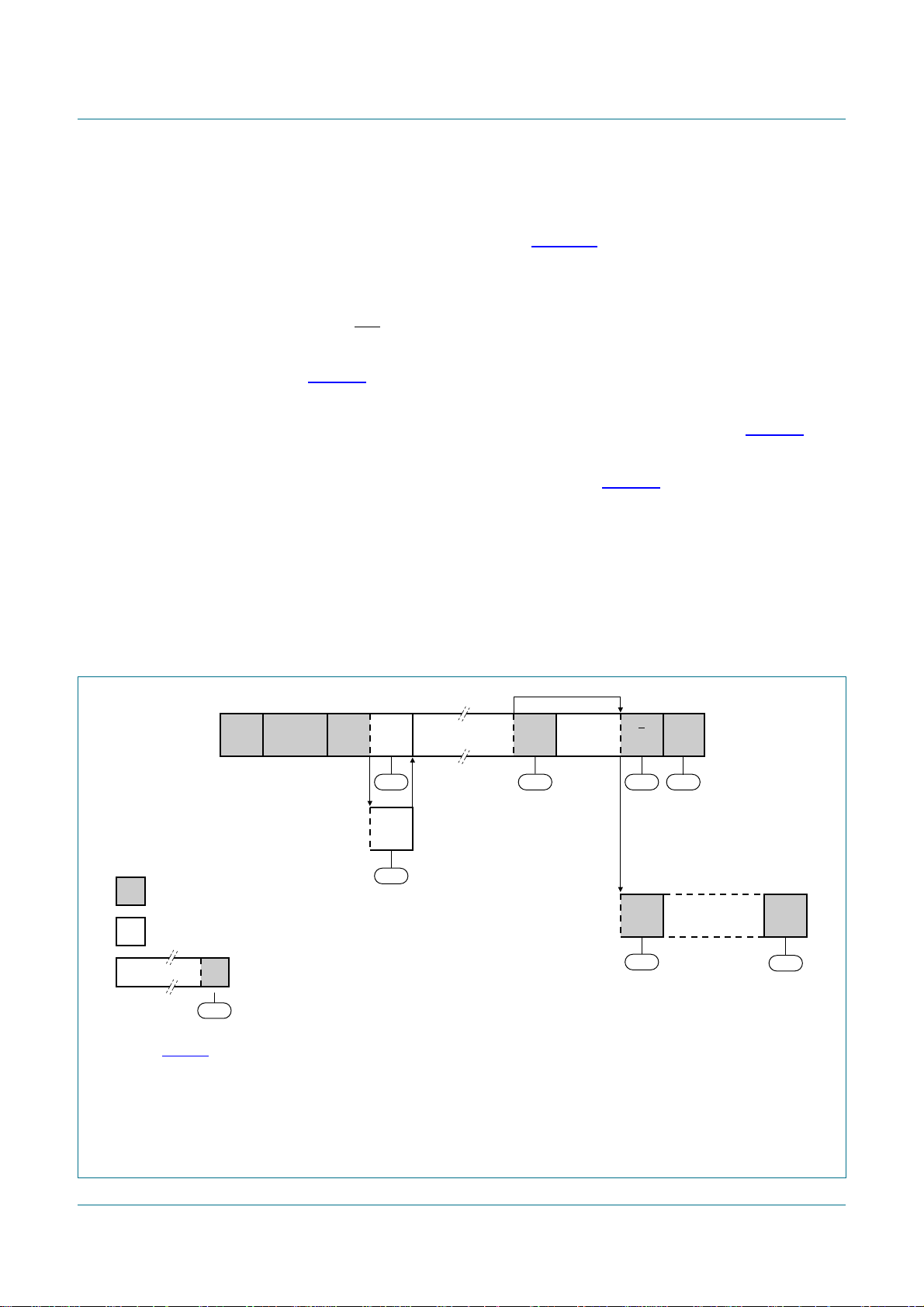
NXP Semiconductors
8.4.4 Slave Transmitter Buffered mode
In the Slave Transmitter Buffered mode, a number of data bytes are transmitted to a
master receiver severalbytesat a time (see Figure 14). Data transfer is initialized as in the
Slave Receiver Buffered mode. When I2CADR and I2CCON have been initialized, the
PCA9665 waits until it is addressed by its own slaveaddress followed by the data direction
bit which must be ‘1’ (R) for the PCA9665 to operate in the Slave Transmitter mode. After
its own slaveaddress and the R bit havebeen received,the Serial Interrupt flag (SI) is set,
the Interrupt line (INT) goes LOW and I2CSTA is loaded with A8h. This status code is
used to vector to an interrupt service routine, and the appropriate action to be taken is
detailed in Table 41.
The Slave Transmitter Buffered mode may also be entered if arbitration is lost while the
PCA9665 is in the master mode. See state B0h and appropriate actions in Table 41.
The byte count register (I2CCOUNT) is programmed with the number of bytes that need
to be sent in a single sequence (BC[6:0]) as shown in Table 39. LB bit is only used for the
Receiver Buffered modes and can be programmed to either logic 0 or logic 1.
If the AA bit is reset during a transfer, the PCA9665 will transmit all the bytes of the
transfer (values defined by BC[6:0]) and enter state C8h. The PCA9665 is switched to the
not addressed slave mode and will ignore the master receiver if it continues the transfer.
Thus the master receiver receives all ‘1’s as serial data. While AA is reset, the PCA9665
does not respond to its own slave address. However, the I2C-bus is still monitored, and
address recognition may be resumed at any time by setting AA. This means that the AA
bit may be used to temporarily isolate the PCA9665 from the I2C-bus.
PCA9665
Fm+ parallel bus to I2C-bus controller
reception of own
slave address and
transmission of one
or more data bytes
arbitration lost as MST and
addressed as slave
from master to slave
from slave to master
DATA
(1) See Table 31.
(2) Defined state when the number of bytes sent is equal to the value in I2CCOUNT register.
(3) Defined state when a NACK is received. The number of bytes transmitted is lower than or equal to the value in the
I2CCOUNT register.
(4) Defined state after the last byte has been transmitted and the PCA9665 goes to the non-addressed mode (AA = 0) and an
ACK is received. The number of bytes that are transmitted is equal to the value in I2CCOUNT register.
S SLA R A
A8h
A
B0h
any number of data bytes and
A
their associated Acknowledge bits
This number (contained in I2CSTA) corresponds
n
to a defined state of the I
2
C-bus.
(1)
A P or S
DATA
B8h F8h
last data byte transmitted;
switched to Not Addressed slave
(AA bit in I2CCON = 0)
DATA A
(2) (3)
C0h
A
C8h
(4)
on STOP
ALL '1's
Fig 14. Format and states in the Slave Transmitter Buffered mode (MODE = 1)
P or S
F8h
on STOP
002aab662
PCA9665_2 © NXP B.V. 2006. All rights reserved.
Product data sheet Rev. 02 — 7 December 2006 45 of 91
Page 46
xxxxxxxxxxxxxxxxxxxxx xxxxxxxxxxxxxxxxxxxxxxxxxx xxxxxxx x x x xxxxxxxxxxxxxxxxxxxxxxxxxxxxxx xxxxxxxxxxxxxxxxxxx xx xx
xxxxx xxxxxxxxxxxxxxxxxxxxxxxxxxx xxxxxxxxxxxxxxxxxxx xxxxxx xxxxxxxxxxxxxxxxxxxxxxxxxxxxxxxxxxx xxxxxxxxxxxx x x
xxxxxxxxxxxxxxxxxxxxx xxxxxxxxxxxxxxxxxxxxxxxxxxxxxx xxxxx xxxxxxxxxxxxxxxxxxxxxxxxxxxxxxxxxxxxxxxxxxxxxxxxxx xxxxxxxx
PCA9665_2 © NXP B.V. 2006. All rights reserved.
Product data sheet Rev. 02 — 7 December 2006 46 of 91
Table 41. Slave Transmitter Buffered mode (MODE = 1)
Status
code
(I2CSTA)
A8h Own SLA+R has
B0h Arbitration lost in
B8h BC[6:0] bytes in
C0h Up to BC[6:0] bytes
xxxxxxxxxxxxxxxxxxxxxxxxx xxxxxxxxxxxxxxxxxxxx xxx
Status of the
2
I
C-bus and the
PCA9665
been received;
ACK has been
returned
SLA+R/W as
master; Own
SLA+R has been
received, ACK has
been returned
I2CDAT have been
transmitted;
ACK has been
received
in I2CDAT have
been transmitted;
NACK has been
received
Application software response Next action taken by the PCA9665
To/from I2CDAT To/from I2CCOUNT To I2CCON
Load data bytesorX Total number of data
Load data bytes X Total number of data
Load data bytesorX Total number of data
Load data bytes X Total number of data
Load data bytesorX Total number of data
Load data bytes X Total number of data
No I2CDAT actionorX X 0 X 0 0 1 Switched to not addressed slave mode;
No I2CDAT actionorX X 0 X 0 1 1 Switched to slave mode; Own slave address
No I2CDAT actionorX X 1 X 0 0 1 Switched to not addressed slave mode;
No I2CDAT action X X 1 X 0 1 1 Switched to slave mode; Own slave address
LB BC[6:0] STA STO SI AA MODE
X X 0 0 1 Up to BC[6:0] bytes will be transmitted.
bytes to be transmitted
X X 0 1 1 Up to BC[6:0] bytes will be transmitted.
bytes to be transmitted
X X 0 0 1 Up to BC[6:0] bytes will be transmitted.
bytes to be transmitted
X X 0 1 1 Up to BC[6:0] bytes will be transmitted.
bytes to be transmitted
X X 0 0 1 Up to BC[6:0] bytes will be transmitted.
bytes to be transmitted
X X 0 1 1 Up to BC[6:0] bytes will be transmitted.
bytes to be transmitted
PCA9665 switches to the not addressed
mode after BC[6:0] bytes have been
transmitted.
PCA9665 switches to the not addressed
mode after BC[6:0] bytes have been
transmitted
PCA9665 switches to the not addressed
mode after BC[6:0] bytes have been
transmitted
No recognition of own slave address;
General Call address recognized if GC = 1
will be recognized; General Call address
recognized if GC = 1
No recognition of own slave address;
General Call address will be recognized if
GC = 1; A START condition will be
transmitted when the bus becomes free
will be recognized; General Call address will
be recognized if GC = 1; A START condition
will be transmitted when the bus becomes
free
NXP Semiconductors
Fm+ parallel bus to I
PCA9665
2
C-bus controller
Page 47
xxxxxxxxxxxxxxxxxxxxx xxxxxxxxxxxxxxxxxxxxxxxxxx xxxxxxx x x x xxxxxxxxxxxxxxxxxxxxxxxxxxxxxx xxxxxxxxxxxxxxxxxxx xx xx
xxxxx xxxxxxxxxxxxxxxxxxxxxxxxxxx xxxxxxxxxxxxxxxxxxx xxxxxx xxxxxxxxxxxxxxxxxxxxxxxxxxxxxxxxxxx xxxxxxxxxxxx x x
xxxxxxxxxxxxxxxxxxxxx xxxxxxxxxxxxxxxxxxxxxxxxxxxxxx xxxxx xxxxxxxxxxxxxxxxxxxxxxxxxxxxxxxxxxxxxxxxxxxxxxxxxx xxxxxxxx
PCA9665_2 © NXP B.V. 2006. All rights reserved.
Product data sheet Rev. 02 — 7 December 2006 47 of 91
Table 41. Slave Transmitter Buffered mode (MODE = 1)
Status
code
(I2CSTA)
C8h BC[6:0] bytes in
xxxxxxxxxxxxxxxxxxxxxxxxx xxxxxxxxxxxxxxxxxxxx xxx
Status of the
2
I
C-bus and the
PCA9665
I2CDAT have been
transmitted
(AA = 0);
ACK has been
received
Application software response Next action taken by the PCA9665
To/from I2CDAT To/from I2CCOUNT To I2CCON
No I2CDAT actionorX X 0 X 0 0 1 Switched to not addressed slave mode;
No I2CDAT actionorX X 0 X 0 1 1 Switched to slave mode; Own slave address
No I2CDAT actionorX X 1 X 0 0 1 Switched to not addressed slave mode;
No I2CDAT action X X 1 X 0 1 1 Switched to slave mode; Own slave address
…continued
LB BC[6:0] STA STO SI AA MODE
NXP Semiconductors
No recognition of own slave address;
General Call address recognized if GC = 1.
will be recognized; General Call address
recognized if GC = 1.
No recognition of own slave address;
General Call address will be recognized if
GC = 1; A START condition will be
transmitted when the bus becomes free.
will be recognized; General Call address will
be recognized if GC = 1; A START condition
will be transmitted when the bus becomes
free.
Fm+ parallel bus to I
PCA9665
2
C-bus controller
Page 48

NXP Semiconductors
8.5 Buffered mode examples
8.5.1 Buffered Master Transmitter mode of operation
1. Program the I2CCOUNT register with the number of bytes that need to be sent to the
2. Load the data bytes in I2CDAT buffer. The different bytes to be sent will be stored in
3. Program I2CCON register to initiate the Master Transmitter Buffered sequence. In
4. After reading the I2CSTA status register, the I2CCON is programmed with STA = 0.
5. When the sequence has been executed, an Interrupt is asserted and the SI bit is set
6. More sequence (program I2CCOUNT register, load data bytes in I2CDAT buffer, write
PCA9665
Fm+ parallel bus to I2C-bus controller
I2C-bus (BC[6:0] has a value from 01h to 44h). LB bit is used for Receiver mode only
and can be set to 0 or 1.
the PCA9665 buffer. There is no protection against writing over a buffer’s boundary. If
more than 68 bytes are written to the buffer, the data at address 00h will be
overwritten. The number of bytes that needs to be loaded in I2CDAT is equal to
BC[6:0] in the I2CCOUNT register. The number of data bytes sent is equal to BC[6:0],
therefore, if the number of data bytes loaded is greater than BC[6:0], the additional
data will not be sent. If the number of data bytes written to the buffer is less than
BC[6:0], the PCA9665 will still send out BC[6:0] data bytes.
Master mode, if STA = 1, a START command is sent. An interrupt will be asserted and
the SI bit is set in the I2CCON register after the START has been sent. The I2CSTA
register contains the status of the transmission. MODE bit must be set to ‘1’ each time
a write to the I2CCON register is performed.
That clears the previous Interrupt. If a START command has been previously sent, the
first byte loaded into the buffer and sent to the I2C-bus is interpreted as the
I2C-bus address + R/W operation. In transmitter mode, R/W = 0 and the following
bytes that are sent to the I2C-bus are interpreted as data bytes.
in the I2CCON register. The I2CSTA register contains the status of the transmission
and the I2CCOUNT register contains the number of bytes that have been sent to the
I2C-bus as described in Table 42.
the I2CCON register to send the data to the I2C-bus, read the I2CSTA register when
the sequence has been executed) can be performed as long as a STOP or Repeated
START command has not been sent. Master Transmitter Buffered mode ends when
the I2CCOUNT register is programmed with STO = 1.
8.5.2 Buffered Master Receiver mode of operation
1. Programthe I2CCOUNT register with the number of bytes that need to be read from a
slave device in the I2C-bus (BC[6:0] has a value from 01h to 44h). LB bit is used in
Receiver mode to let the PCA9665 know if the last byte received must be
acknowledged or not.
LB = 0: Last received byte is acknowledged and another sequence can be executed.
LB = 1: Last received byte is not acknowledged. The last sequence before sending a
STOP or Repeated START must be executed with LB = 1.
2. Load the I2C-bus address + R/W = 1 in I2CDAT buffer.
PCA9665_2 © NXP B.V. 2006. All rights reserved.
Product data sheet Rev. 02 — 7 December 2006 48 of 91
Page 49

NXP Semiconductors
3. Program I2CCON register to initiate the Master Receiver Buffered sequence. In
4. After reading the I2CSTA status register, the I2CCON is programmed with STA = 0.
5. When the sequence has been executed, an Interrupt is asserted and the SI bit is set
6. Moresequences (program the I2CCOUNT register,write to the I2CCON register, read
PCA9665
Fm+ parallel bus to I2C-bus controller
Master mode, if STA = 1, a START command is sent. An interrupt will be asserted and
the SI bit is set in the I2CCON register after the START has been sent. The I2CSTA
register contains the status of the transmission. MODE bit must be set to ‘1’ each time
a write to the I2CCON register is performed.
That clears the previous Interrupt. If a START command has been previously sent, the
I2C-bus address + R/W = 1 byte that has been loaded into the buffer is sent to the
I2C-bus, the PCA9665 then becomes a master receiver device and starts receiving
data from the addressed slave device.
Remark: The PCA9665 is already a master receiver device if a buffered sequence
has been previously executed.
in the I2CCON register. The I2CSTA register contains the status of the transmission
and the I2CCOUNT register contains the number of bytes that have been received.
I2CDAT buffer contains all the data that has been received and can be read by the
microcontroller.
the I2CSTA register when sequence has been executed, read the I2CDAT buffer) can
be performed as long as a STOP or a Repeated START command has not been sent.
To be able to end the reception, the last buffered sequence must be performed with
LB = 1. Master Receiver Buffered mode ends when the I2CCOUNT register is
programmed with STO = 1.
8.5.3 Buffered Slave Transmitter mode
1. An interrupt is asserted and the SI bit is set in the I2CCON register when the
PCA9665’s own slave address has been detected on the I2C-bus (AA = 1, own slave
address defined in the I2CADR register). In Slave Transmitter mode, R/W=1.
2. Program the I2CCOUNT register with the number of bytes that need to be sent to the
I2C-bus (BC[6:0] has a value from 01h to 44h). LB bit is used for Receiver Buffered
mode only.
3. Load the data bytes in I2CDAT buffer. The different bytes to be sent will be stored in
the PCA9665 buffer. There is no protection against writing over a buffer’s boundary. If
more than 68 bytes are written to the buffer, the data at address 00h will be
overwritten. The number of bytes that needs to be loaded in I2CDAT is equal to
BC[6:0] in the I2CCOUNT register. The number of data bytes sent is equal to BC[6:0],
therefore, if the number of data bytes loaded is greater than BC[6:0], the additional
data will not be sent. If the number of data bytes written to the buffer is less than
BC[6:0], the PCA9665 will still send out BC[6:0] data bytes.
4. The I2CCON is programmed to clear the previous Interrupt. The bytes loaded into the
buffer are sent to the I2C-bus. MODE bits must be set to ‘1’ each time a write to the
I2CCON register is performed.
5. When the sequence has been executed (BC[6:0] bytes sent or the master sent a
NACK), an Interrupt is asserted and the SI bit is set in the I2CCON register. The
I2CSTA register contains the status of the transmission and the I2CCOUNT register
contains the number of bytes that have been sent to the I2C-bus.
PCA9665_2 © NXP B.V. 2006. All rights reserved.
Product data sheet Rev. 02 — 7 December 2006 49 of 91
Page 50

NXP Semiconductors
6. More sequences (program I2CCOUNT register, load data bytes in I2CDAT buffer,
8.5.4 Buffered Slave Receiver mode
1. An interrupt is asserted and the SI bit is set in the I2CCON register when the
2. Program the I2CCOUNT register with the number of bytes that needs to be read from
3. The I2CCON is programmed to clear the previous Interrupt. The PCA9665 receives
4. When the sequence has been executed (BC[6:0] bytes have been received or the
5. More sequence (program the I2CCOUNT register, write to the I2CCON register, read
PCA9665
Fm+ parallel bus to I2C-bus controller
write the I2CCON register to send the data to the I2C-bus, read the I2CSTA register
when sequence has been executed) can be performed as long as the master
acknowledgesthe bytes sent by the PCA9665 and AA = 1. SlaveTransmitter Buffered
mode ends when the I2C-bus master does not acknowledge a byte or when the
PCA9665 goes to Non-addressed Slave mode.
PCA9665‘s own slave address has been detected in the I2C-bus (AA = 1, own slave
address defined in the I2CADR register). In Slave Receiver mode, R/W=0.
a master device in the I2C-bus (BC[6:0] has a value from 01h to 44h). LB bit is used in
Receiver mode to let the PCA9665 know if the last byte received must be
acknowledged or not.
LB = 0: Last received byte is acknowledged and another sequence can be executed.
LB = 1: Last received byte is not acknowledged.
data from the I2C-bus master. MODE bit must be set to ‘1’ each time a write to the
I2CCON register is performed.
master sent a STOP or Repeated START command), an Interrupt is asserted and the
SI bit is set in the I2CCON register. The I2CSTA register contains the status of the
transmission and the I2CCOUNT register contains the number of bytes that have
been received. I2CDAT buffer contains all the data that has been received and can be
read by the microcontroller.
the I2CDAT buffer) can be performed as long as a STOP or a Repeated START
command has not been sent by the I2C-bus master. Slave Receiver Buffered mode
ends when the I2C-bus master sends a STOP or Repeated START command, or
when the PCA9665 does not acknowledge the received bytes any more.
8.5.5 Example: Read 128 bytes in two 64-byte sequences of an EEPROM
2
(I
C-bus address = A0h for write operations and A1h for read operations)
starting at Location 08h
1. Program I2CCOUNT = 02h (2 bytes to be sent): I2C-bus slave address and memory
allocation.
2. Write A0h (I2C-bus slave address and write command) and 08h (Location) into the
I2CDAT register.
3. Program I2CCON with STA = 1, STO = SI = 0, MODE = 1.
– the PCA9665 sends a START command
– the PCA9665 sends an interrupt, sets SI = 1 and updates I2CSTA register
– I2CSTA reads 08h
4. Program I2CCON with STA = STO = SI = 0, MODE = 1.
– I2C-bus slave address A0h, then EEPROM sub address 08h is sent on the bus
PCA9665_2 © NXP B.V. 2006. All rights reserved.
Product data sheet Rev. 02 — 7 December 2006 50 of 91
Page 51

NXP Semiconductors
5. Program I2CCOUNT = 40h (64 bytes to read and Last byte acknowledged).
6. Load I2CDAT with A1h (I2C-bus slave address and Read command).
7. Program I2CCON with STA = 1, SI = 0, MODE = 1.
8. Program I2CCON with STA = STO = SI = 0, MODE = 1.
9. The microcontroller reads the 64 data bytes from the PCA9665.
10. Program I2CCOUNT = C0h (64 bytes and Last byte is not acknowledged).
11. Program I2CCON with STA = STO = SI = 0, MODE = 1.
12. The PCA9665 reads 64 bytes and does not acknowledge the last byte.
13. The microcontroller reads the 64 bytes from the PCA9665.
14. Program I2CCON with SI = STA = 0, ST0 = 1, MODE = X.
PCA9665
Fm+ parallel bus to I2C-bus controller
– the SCL line is held LOW by the PCA9665 after the 2 bytes have been sent
– the PCA9665 sends an Interrupt, sets SI = 1 and updates I2CSTA register
– I2CSTA reads 28h
– the PCA9665 sends a ReSTART command
– an interrupt is asserted and the I2CSTA register is updated
– the I2CSTA register reads 10h
– address A1h is sent followed by a read of 64 data bytes
– the last data byte is acknowledged
– the SCL line is held LOW by the PCA9665 after the data is read
– the PCA9665 sends an interrupt and updates I2CSTA register
– I2CSTA reads 50h
– the PCA9665 sends an Interrupt and updates I2CSTA register
– the I2CSTA reads 58h
– the SCL line is held LOW by the PCA9665
– the slave should release the SDA line
– the PCA9665 sends a STOP condition
– no interrupt is generated by the PCA9665
– the I2CSTA register contains F8h
8.6 I2CCOUNT register
When a write to the I2CCOUNT register is requested, the bufferpointer is reset and points
at the first byte. Loading of the data in the I2CDAT buffer then starts at the first byte.
Once an operation has been performed (SI = 1 and an interrupt is generated), the
I2CCOUNT register contains the number of bytes that have been received (Receiver
mode) or the number of bytes that have been sent (Transmitter mode). See Table 42 for
more information.
In Buffered Transmitter mode, the first byte that is sent to the I2C-bus is always the first
byte that has been loaded in the I2CDAT buffer.
PCA9665_2 © NXP B.V. 2006. All rights reserved.
Product data sheet Rev. 02 — 7 December 2006 51 of 91
Page 52

NXP Semiconductors
PCA9665
Fm+ parallel bus to I2C-bus controller
In Buffered Receiver mode, when an interrupt is generated and SI is set to 1 (after a
STOP command or a buffer full condition), the buffer pointer is reset and points at the first
received data byte. Reading the I2CCOUNT register then indicates the number of bytes
that have been sent or received (BC[6:0]). Reading of the data from I2CDAT buffer can
then be initiated starting with the first received byte.
Table 42. I2CCOUNT register value based on the performed operation
Operation performed I2CCOUNT register value
Master Transmitter Buffered mode
After START condition don’t care
After Slave Address Sent + ACK bit received and interrupt received 1
After Slave Address Sent + NACK bit received 1
After Slave Address Sent + ‘n’ data bytes sent, ACK bit received, both
address and ‘n’ data
After Slave Address Sent + ‘n’ data bytes sent, last byte n + 1
After STOP don’t care
After losing arbitration in Slave Address + W and addressed as slave 0
After losing arbitration in slave address + W and not addressed as slave 0
th
After losing arbitration in data at n
Master Receiver Buffered mode
After START condition don't care
After Slave Address Sent + ACK bit received don't care (because no interrupt received here)
After Slave Address Sent + NACK bit received 1
After Slave Address Sent + ‘n’ data bytes received, ACK bit received for
address and ACK bit returned for ‘n’ data bytes
After Slave Address Sent + ‘n’ data bytes received, NACK bit returned
for the last byte
After STOP don't care
After losing arbitration in Slave Address + R bit and addressed as slave 0
After losing arbitration in slave address + R and not addressed as slave 0
After losing arbitration in ACK of n
Slave Receiver Buffered mode (regular slave mode and General Call response
After SlaveAddress + W and ACKbit returned for slave address (both in
regular mode and when PCA9665 loses arbitration and is addressed as
slave)
After receiving ‘n’ bytes, ACK bit returned for the ‘n’ bytes n
After receiving ‘n’ bytes, NACK bit returned for the last byte n
Slave Transmitter Buffered mode
After Slave Address + R and ACK bit returned for slave address (both in
regular mode and when PCA9665 loses arbitration and is addressed as
slave)
After ‘n’ data bytes transmitted and ACK bit received for ‘n’ bytes n
After ‘n’ data bytes transmitted and NACK bit received for the last byte n
byte n (if there was no interrupt after slave address was
th
byte n
n+1
sent)
n − 1 (if there was an interrupt after slave address
was sent)
n
n
0
0
PCA9665_2 © NXP B.V. 2006. All rights reserved.
Product data sheet Rev. 02 — 7 December 2006 52 of 91
Page 53

NXP Semiconductors
Remark: Request to send or receive a number of bytes equal to 0 or higher than 68
(BC[6:0] = 000 0000 or BC[6:0] > 100 0100) will cause no data to be transferred and an
interrupt to be generated after writing to the I2CCON register. I2CSTA status register is
loaded with FCh that indicates that an invalid value was requested to be loaded in
I2CCOUNT.
8.7 Acknowledge management (I2C-bus addresses and data) in Byte and Buffered modes
Data acknowledge/not acknowledge management can be controlled on a byte basis (Byte
mode) or on a sequence basis (Buffered mode). The PCA9665 can be programmed to
respond (ACK) or not (NACK) to two differentI2C-bus addresses. Table 43 shows how this
is performed based on the different control bits (AA, GC, LB and MODE) and the different
modes.
Table 43. Own slave address, General Call address, and Data acknowledge management
AA GC LB MODE Address Data received
Master mode: the PCA9665 generates a START command and controls the I2C-bus
0 X X 0 not applicable data (each byte) = NACK
1 X X 0 not applicable data (each byte) = ACK
X X 0 1 not applicable all the bytes (BC[6:0] bytes) = ACK
X X 1 1 not applicable all the bytes except the last one
Slave mode: I
0 X X 0 Own address = NACK data (each byte)= NACK
1 X X 0 Own address = ACK data (each byte) = ACK
0 X 0 1 Own address = NACK all the bytes (≤ BC[6:0] bytes) = ACK
0 X 1 1 Own address = NACK all the bytes except the last one
1 X 0 1 Own address = ACK all the bytes (≤ BC[6:0] bytes) = ACK
1 X 1 1 Own address = ACK all the bytes except the last one
Slave mode: I2C-bus message starting with the General Call address
X 0 X 0 GC address = NACK data (each byte) = NACK
0 1 X 0 GC address = ACK data (each byte) = NACK
1 1 X 0 GC address = ACK data (each byte) = ACK
X 0 X 1 GC address = NACK data (each byte) = NACK
X 1 0 1 GC address = ACK all the bytes (≤ BC[6:0] bytes) = ACK
X 1 1 1 GC address = ACK all the bytes except the last one
PCA9665
Fm+ parallel bus to I2C-bus controller
[1]
(BC[6:0] bytes − 1) = ACK;
last byte = NACK
2
C-bus message starting with the PCA9665’s Own Slave address
(BC[6:0] bytes - 1) = ACK; last
byte=NACK
(BC[6:0] bytes - 1) = ACK;
last byte = NACK
(BC[6:0] bytes - 1) = ACK;
last byte = NACK
[2]
[2]
[2]
[1] Assumption is that Data Received follows the address (as defined in column “Address”); valid for slave
mode only.
[2] Unless the master sends a STOP command before.
PCA9665_2 © NXP B.V. 2006. All rights reserved.
Product data sheet Rev. 02 — 7 December 2006 53 of 91
Page 54

NXP Semiconductors
Table 44. Unbuffered Mode (MODE = 0)
Control
bits
AA = 0 Master Transmitter mode
• address/data are transmitted on a byte basis
Slave Transmitter mode
• NACK returned after own slave address received
• switch to not addressed slave mode any time
during an I
AA = 1 Master Transmitter mode
2
C-bus sequence
• address/data are transmitted on a byte basis
Slave Transmitter mode
• ACK returned after own slave address received
• always addressed during an I
2
C-bus sequence
PCA9665
Fm+ parallel bus to I2C-bus controller
LB = x
Master Receiver mode
• address is transmitted and data are received on a
byte basis
• NACK returned after one byte received
Slave Receiver mode
• NACK returned after own slave address received
• NACK returned after one byte received
Master Receiver mode
• data are received on a byte basis
• ACK returned after one byte received
Slave Receiver mode
• ACK returned after own slave address received
• ACK returned after one byte received
PCA9665_2 © NXP B.V. 2006. All rights reserved.
Product data sheet Rev. 02 — 7 December 2006 54 of 91
Page 55

NXP Semiconductors
Table 45. Buffered Mode (MODE = 1)
Control
bits
AA = 0 Master Transmitter
mode
LB=0 LB=1
Master Receiver mode
• address is transmitted
• address/data are
transmitted on a
multiple byte basis
= BC[6:0] value
Slave Transmitter
mode
• ACK returned after the
Slave Receiver mode
• NACK returned after own
• NACK returned
after own slave
address received
• in addressed mode, data
• in addressed
mode, data are
transmitted on a
multiple byte basis
= BC[6:0] value
• in addressed mode, ACK
• in addressed
mode, switch to
non addressed
mode after the last
byte of a buffered
sequence is
transmitted (after
bytes sent
= BC[6:0] value)
• in addressed mode,
and data are received on
a multiple byte basis
= BC[6:0] value
last byte of a buffered
sequence received (after
bytes received = BC[6:0]
value)
slave address received
are received on a multiple
byte basis = BC[6:0]
value
returned after the last
byte of a buffered
sequence received (after
bytes received = BC[6:0]
value)
switch to non-addressed
mode after the last byte of
a buffered sequence is
received (after bytes
received = BC[6:0] value)
Fm+ parallel bus to I2C-bus controller
Master Transmitter mode
• address/data are
transmitted on a
multiple byte basis
= BC[6:0] value
Slave Transmitter mode
• NACKreturnedafter
own slave address
received
• in addressed mode,
data are transmitted
on a multiple byte
basis = BC[6:0]
value
• in addressed mode,
switch to non
addressed mode
after the last byte of
a buffered
sequence is
transmitted (after
bytessent= BC[6:0]
value)
PCA9665
Master Receiver mode
• address is transmitted
and data are received on
a multiple byte basis
= BC[6:0] value
• NACK returned after the
last byte of a buffered
sequencereceived(after
bytes received = BC[6:0]
value)
Slave Receiver mode
• NACK returned after
own slave address
received
• in addressed mode, data
are received on a
multiple byte basis
= BC[6:0] value
• in addressed mode,
NACK returned after the
last byte of a buffered
sequencereceived(after
bytes received = BC[6:0]
value)
• in addressed mode,
switch to non-addressed
mode after the last byte
of a buffered sequence
is received (after bytes
received = BC[6:0]
value)
PCA9665_2 © NXP B.V. 2006. All rights reserved.
Product data sheet Rev. 02 — 7 December 2006 55 of 91
Page 56

NXP Semiconductors
PCA9665
Fm+ parallel bus to I2C-bus controller
Table 45. Buffered Mode (MODE = 1)
Control
bits
AA = 1 Master Transmitter
mode
LB=0 LB=1
Master Receiver mode
• address is transmitted
• address/data are
transmitted on a
multiple byte basis
= BC[6:0] value
Slave Transmitter
mode
• ACK returned after the
Slave Receiver mode
• ACK returned after own
• ACKreturnedafter
own slaveaddress
received
• in addressed mode, data
• in addressed
mode, data are
transmitted on a
multiple byte basis
= BC[6:0] value
• in addressed mode, ACK
• always addressed
during a buffered
sequence
…continued
and data are received on
a multiple byte basis
= BC[6:0] value
last byte of a buffered
sequence received (after
bytes received = BC[6:0]
value)
slave address received
are received on a multiple
byte basis = BC[6:0]
value
returned after the last
byte of a buffered
sequence received (after
bytes received = BC[6:0]
value)
Master Transmitter mode
• address/data are
transmitted on a
multiple byte basis
= BC[6:0] value
Slave Transmitter mode
• ACK returned after
own slave address
received
• in addressed mode,
data are transmitted
on a multiple byte
basis = BC[6:0]
value
• always addressed
during a buffered
sequence
Master Receiver mode
• address is transmitted
and data are received on
a multiple byte basis
= BC[6:0] value
• NACK returned after the
last byte of a buffered
sequencereceived(after
bytes received = BC[6:0]
value)
Slave Receiver mode
• ACK returned after own
slave address received
• in addressed mode, data
are received on a
multiple byte basis
= BC[6:0] value
• in addressed mode,
NACK returned after the
last byte of a buffered
sequencereceived(after
bytes received = BC[6:0]
value)
PCA9665_2 © NXP B.V. 2006. All rights reserved.
Product data sheet Rev. 02 — 7 December 2006 56 of 91
Page 57

NXP Semiconductors
8.8 Miscellaneous states
There are four I2CSTA codes that do not correspond to a defined PCA9665 state (see
Table 46). These are discussed in Section 8.8.1 through Section 8.8.4.
Table 46. Miscellaneous states
Status
code
(I2CSTA)
F8h On hardware or
70h Bus error
78h Bus error
FCh Illegal value in
00h Bus error during
StatusoftheI2C-bus
and the PCA9665
software reset or
STOP
SDA stuck LOW
SCL stuck LOW
I2CCOUNT
masterorslavemode,
due to illegal START
or STOP condition
PCA9665
Fm+ parallel bus to I2C-bus controller
Application software response Next action taken by PCA9665
To/from I2CDAT To I2CCON
STA STO SI AA MODE
No I2CDAT action 1 X 0 X X Go into master mode; send START
No I2CDAT action 0 X 0 0 X No recognition of own slave
address. General Call address will
be recognized if GC = 1.
No I2CDAT action 0 X 0 1 X Will recognize own slave address.
General Call address will be
recognized if GC = 1.
No I2CDAT action No I2CCON action Hardware or software reset of the
PCA9665 (requires reset to return
to state F8h)
No I2CDAT action No I2CCON action Hardware or software reset of the
PCA9665 (requires reset to return
to state F8h)
No I2CDAT action No I2CCON action Program a valid value in
I2CCOUNT:BC[6:0]between1and
68.
No I2CDAT action No I2CCON action Hardware or software reset of the
PCA9665 (requires reset to return
to state F8h)
8.8.1 I2CSTA = F8h
This status code indicates that the PCA9665 is in an idle state and that no relevant
information is availablebecause the serial interrupt flag, SI, is not yet set. This occurs on a
STOP condition or during a hardware or software reset event and when the PCA9665 is
not involved in a serial transfer.
8.8.2 I2CSTA = 00h
This status code indicates that a bus error has occurred during a serial transfer. A bus
error is caused when a START or STOP condition occurs at an illegal position in the
format frame. Examples of such illegal positions are during the serial transfer of an
address byte, a data byte, or an acknowledge bit. A bus error may also be caused when
external interference disturbs the internal PCA9665 signals. When a bus error occurs, SI
is set. To recover from a bus error, the microcontroller must send an external hardware or
software reset signal to reset the PCA9665.
8.8.3 I2CSTA = 70h
This status code indicates that the SDA line is stuck LOW when the PCA9665, in master
mode, is trying to send a START condition.
PCA9665_2 © NXP B.V. 2006. All rights reserved.
Product data sheet Rev. 02 — 7 December 2006 57 of 91
Page 58
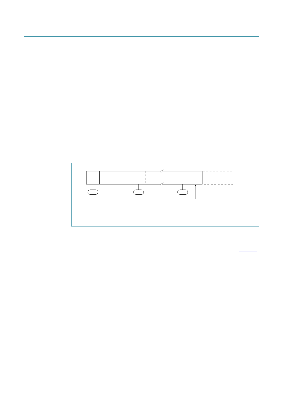
NXP Semiconductors
8.8.4 I2CSTA = 78h
This status code indicates that the SCL line is stuck LOW.
8.9 Some special cases
The PCA9665 has facilities to handle the following special cases that may occur during a
serial transfer.
8.9.1 Simultaneous repeated START conditions from two masters
A repeated START condition may be generated in the Master Transmitter or Master
Receiver modes. A special case occurs if another master simultaneously generates a
repeated START condition (see Figure 15). Until this occurs, arbitration is not lost by
either master since they were both transmitting the same data.
If the PCA9665 detects a repeated START condition on the I2C-bus before generating a
repeated START condition itself, it will use the repeated START as its own and continue
with the sending of the slave address.
PCA9665
Fm+ parallel bus to I2C-bus controller
S SLA W A
08h
Fig 15. Simultaneous repeated START conditions from 2 masters
18h
DATA
8.9.2 Data transfer after loss of arbitration
Arbitration may be lost in the Master Transmitter and Master Receiver modes. Loss of
arbitration is indicated by the following states in I2CSTA; 38h, 68h, and B0h (see Figure 7,
Figure 11, Figure 8, and Figure 12).
Remark: In order to exit state 38h, a Time-out, Reset, or external STOP are required.
If the STA flag in I2CCON is set by the routines which service these states, then, if the bus
is free again, a START condition (state 08h) is transmitted without intervention by the
CPU, and a retry of the total serial transfer can commence.
8.9.3 Forced access to the I2C-bus
In some applications, it may be possible for an uncontrolled source to cause a bus
hang-up. In such situations, the problem may be caused by interference, temporary
interruption of the bus or a temporary short-circuit between SDA and SCL.
28h
A
both masters continue
S
with SLA transmission
other master sends
repeated START condition earlier
002aab028
If an uncontrolled source generates a superfluous START or masks a STOP condition,
then the I2C-bus stays busy indefinitely. If the STA flag is set and bus access is not
obtained within a reasonable amount of time, then a forced access to the I2C-bus is
possible. If the I2C-bus stays idle for a time period equal to the time-out period, then the
PCA9665 concludes that no other master is using the bus and sends a START condition.
PCA9665_2 © NXP B.V. 2006. All rights reserved.
Product data sheet Rev. 02 — 7 December 2006 58 of 91
Page 59
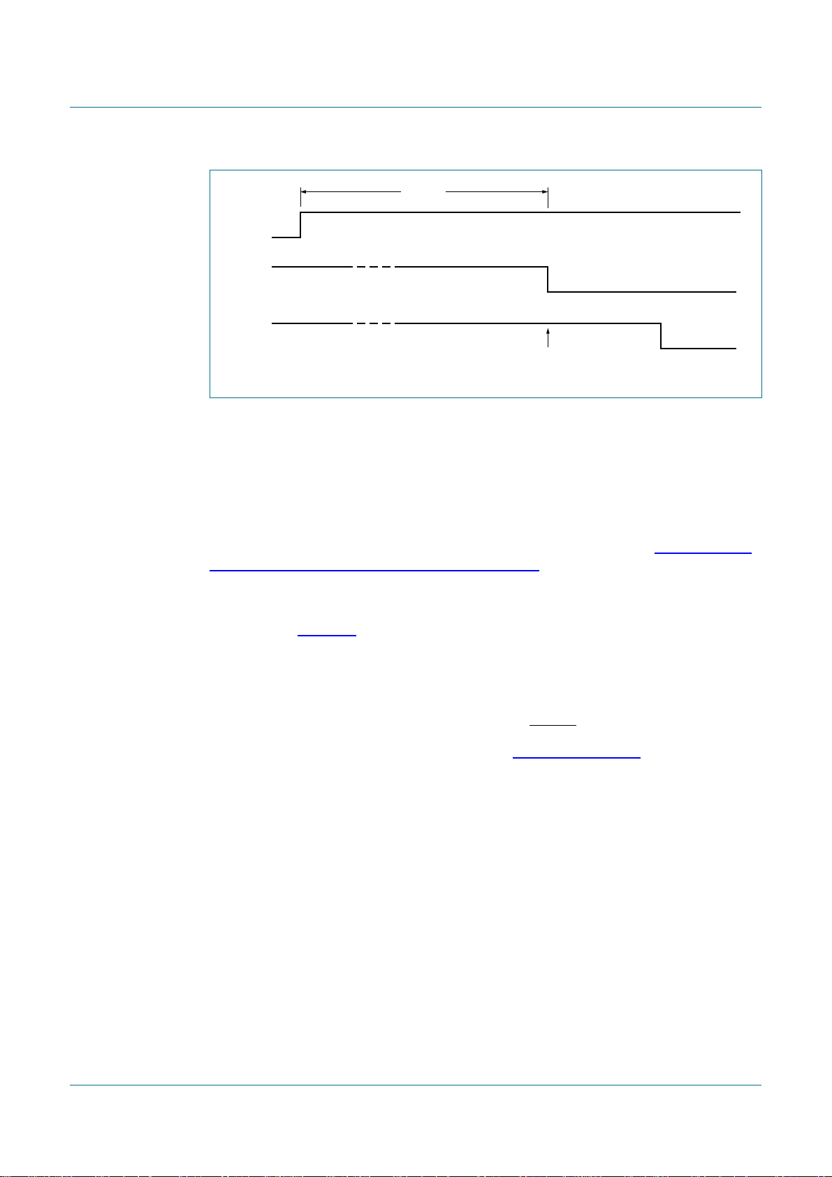
NXP Semiconductors
Fig 16. Forced access to a busy I2C-bus
8.9.4 I2C-bus obstructed by a LOW level on SCL or SDA
An I2C-bus hang-up occurs if SDA or SCL is pulled LOW by an uncontrolled source. If the
SCL line is obstructed (pulled LOW) by a device on the bus, no further serial transfer is
possible, and the PCA9665 cannot resolve this type of problem. When this occurs, the
problem must be resolved by the device that is pulling the SCL bus line LOW.
STA flag
SDA line
SCL line
PCA9665
Fm+ parallel bus to I2C-bus controller
time-out
START condition
002aab029
When the SCL line stays LOW for a period equal to the time-out value, the PCA9665
concludes that this is a bus error and behaves in a manner described in Section 7.3.2.4
“The Time-out register, I2CTO (indirect address 04h)”.
If the SDA line is obstructed by another device on the bus (e.g., a slave device out of bit
synchronization), the problem can be solved by transmitting additional clock pulses on the
SCL line (see Figure 17). The PCA9665 sends out nine clock pulses followed by the
STOP condition. If the SDA line is released by the slave pulling it LOW, a normal START
condition is transmitted by the PCA9665, state 08h is entered and the serial transfer
continues. If the SDA line is not released by the slave pulling it LOW, then the PCA9665
concludes that there is a bus error, loads 70h in I2CSTA, generates an interrupt signal,
and releases the SCL and SDA lines. After the microcontroller reads the status register, it
needs to send a reset signal (hardware through the RESET pin, or software through the
parallel port) in order to reset the PCA9665. See Section 8.11 “Reset” for more
information.
If a forced bus access occurs or a repeated START condition is transmitted while SDA is
obstructed (pulled LOW), the PCA9665 performs the same action as described above. In
each case, state 08h is entered after a successful START condition is transmitted and
normal serial transfer continues. Note that the CPU is not involved in solving these bus
hang-up problems.
PCA9665_2 © NXP B.V. 2006. All rights reserved.
Product data sheet Rev. 02 — 7 December 2006 59 of 91
Page 60
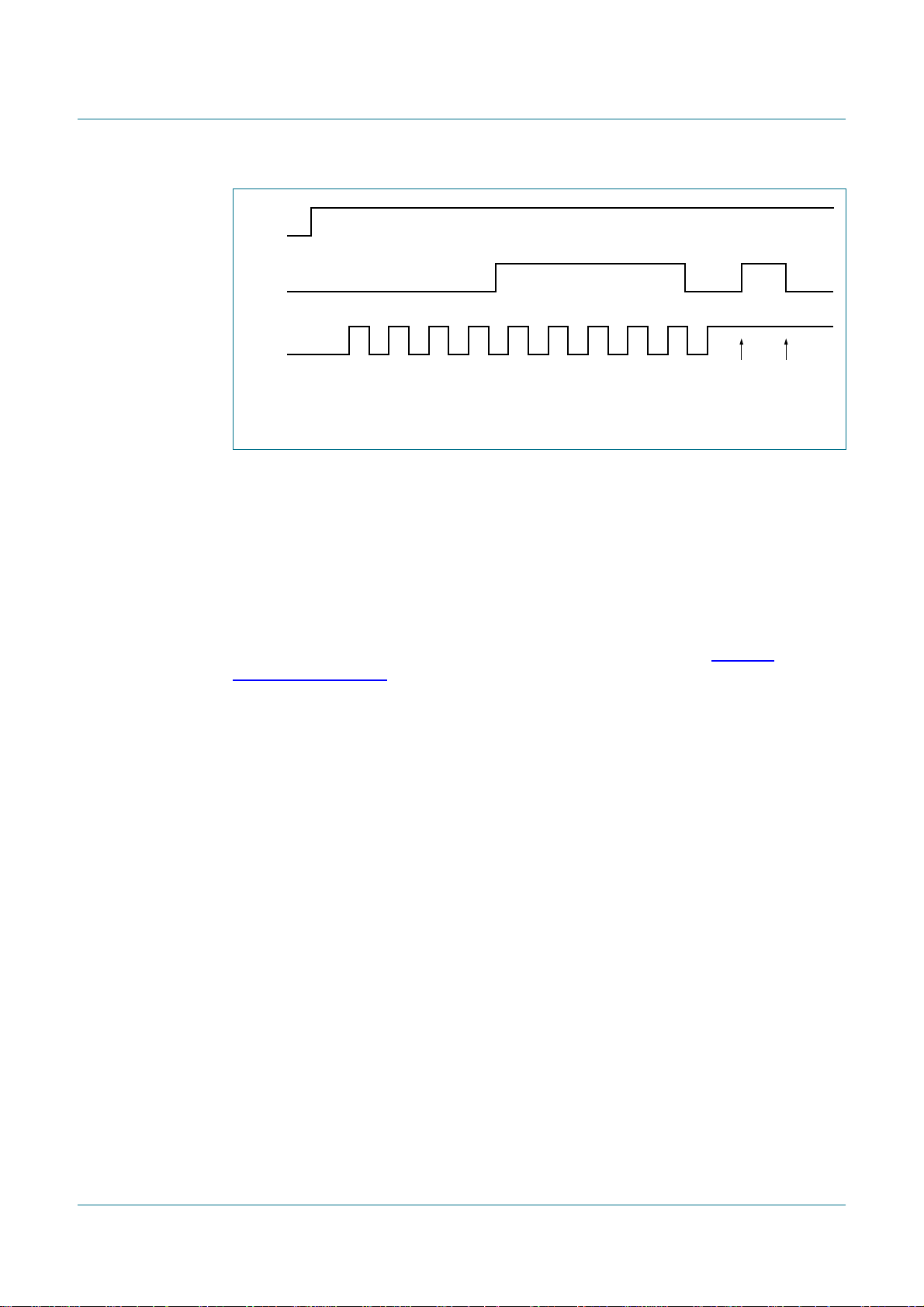
NXP Semiconductors
STA flag
SDA line
SCL line
PCA9665
Fm+ parallel bus to I2C-bus controller
123456789
Fig 17. Recovering from a bus obstruction caused by a LOW level on SDA
8.9.5 Bus error
A bus error occurs when a START or STOP condition is present at an illegal position in the
format frame. Examples of illegal positions are during the serial transfer of an address
byte, a data or an acknowledge bit.
The PCA9665 only reacts to a bus error when it is involved in a serial transfer either as a
master or an addressed slave. When a bus error is detected, PCA9665 releases the SDA
and SCL lines, sets the interrupt flag, and loads the status register with 00h. This status
code may be used to vector to a service routine which either attempts the aborted serial
transfer again or simply recovers from the error condition as shown in Table 46
“Miscellaneous states”. The microcontroller must send an external hardware or software
reset signal to reset the PCA9665.
8.10 Power-on reset
When power is applied to VDD, an internal Power-On Reset holds the PCA9665 in a reset
condition until VDDhas reached V
PCA9665 goes to the power-up initialization phase where the following operations are
performed:
STOP
condition
. At this point, the reset condition is released and the
POR
START
condition
002aab030
1. ENSIO bit is set to 1 to enable the internal oscillator.
2. Internal register initialization is performed.
3. ENSIO bit is set to 0 to disable the internal oscillator and go to the non-addressed low
power mode.
The complete power-up initialization phase takes 550 µs to be performed. During this
time, write to the PCA9665 through the parallel port is not permitted. However, the parallel
port can be read. This allows the device connected to the parallel port of the PCA9665 to
poll the I2CCON register and read the ENSIO state bit. When ENSIO bit is equal to 1, this
means that the power-up initialization is in progress. When ENSIO is set to 0, this means
that the power-up initialization is done and that the PCA9665 is initialized and ready to be
used.
PCA9665_2 © NXP B.V. 2006. All rights reserved.
Product data sheet Rev. 02 — 7 December 2006 60 of 91
Page 61
NXP Semiconductors
8.11 Reset
Reset of the PCA9665 to its default state can be performed in 2 different ways:
PCA9665
Fm+ parallel bus to I2C-bus controller
• By holding the RESET pin LOW for a minimum of t
• By using the Parallel Software Reset sequence as described in Figure 18.
access to INDPTR
Indirect Register pointer
A[1:0] 00
I2CPRESET register selected
D[7:0] 05h
WR
If D[7:0] ≠ A5h,
following byte is ignored
and reset is aborted.
internal
reset
signal
Fig 18. Parallel Software Reset sequence
8.12 I2C-bus timing diagrams, Unbuffered mode
The diagrams (Figure 19 through Figure 22) illustrate typical timing diagrams for the
PCA9665 in master/slave functions.
access to the INDIRECT
Indirect Data field
10
SWRST data byte 1
A5h
If D[7:0] ≠ 5Ah, reset is aborted.
If SWRST Data 1 = A5h and
SWRST Data 2 = 5Ah, PCA9665
is reset to its default state.
.
w(rst)
SWRST data byte 2
5Ah
002aab966
SCL
SDA
INT
START
condition
from slave receiver
7-bit address
R/W = 0
ACK
interrupt
first byte
interrupt
ACK
Master PCA9665 writes data to slave transmitter.
Fig 19. Bus timing diagram; Unbuffered Master Transmitter mode
n byte
ACK
interrupt
STOP
condition
002aab031
PCA9665_2 © NXP B.V. 2006. All rights reserved.
Product data sheet Rev. 02 — 7 December 2006 61 of 91
Page 62
NXP Semiconductors
SCL
SDA
PCA9665
Fm+ parallel bus to I2C-bus controller
INT
START
condition
7-bit address
R/W = 1
from slave
ACK
interrupt
first byte
ACK
Master PCA9665 reads data from slave transmitter.
Fig 20. Bus timing diagram; Unbuffered Master Receiver mode
SCL
SDA
INT
START
condition
7-bit address
from slave PCA9665
R/W = 1
(1)
ACK
interrupt
first byte
ACK
External master receiver reads data from PCA9665.
(1) As defined in I2CADR register.
Fig 21. Bus timing diagram; Unbuffered Slave Transmitter mode
interrupt
from master receiver
interrupt
from master receiver
n byte
n byte
no ACK
no ACK
STOP
condition
002aab032
interrupt
STOP
condition
002aab033
SCL
SDA
INT
START
condition
7-bit address
from slave PCA9665
R/W = 0
(1)
ACK
interrupt
first byte
ACK
interrupt
n byte
ACK
interrupt
interrupt
(after STOP)
STOP
condition
002aab034
Slave PCA9665 is written to by external master transmitter.
(1) As defined in I2CADR register.
Fig 22. Bus timing diagram; Unbuffered Slave Receiver mode
PCA9665_2 © NXP B.V. 2006. All rights reserved.
Product data sheet Rev. 02 — 7 December 2006 62 of 91
Page 63
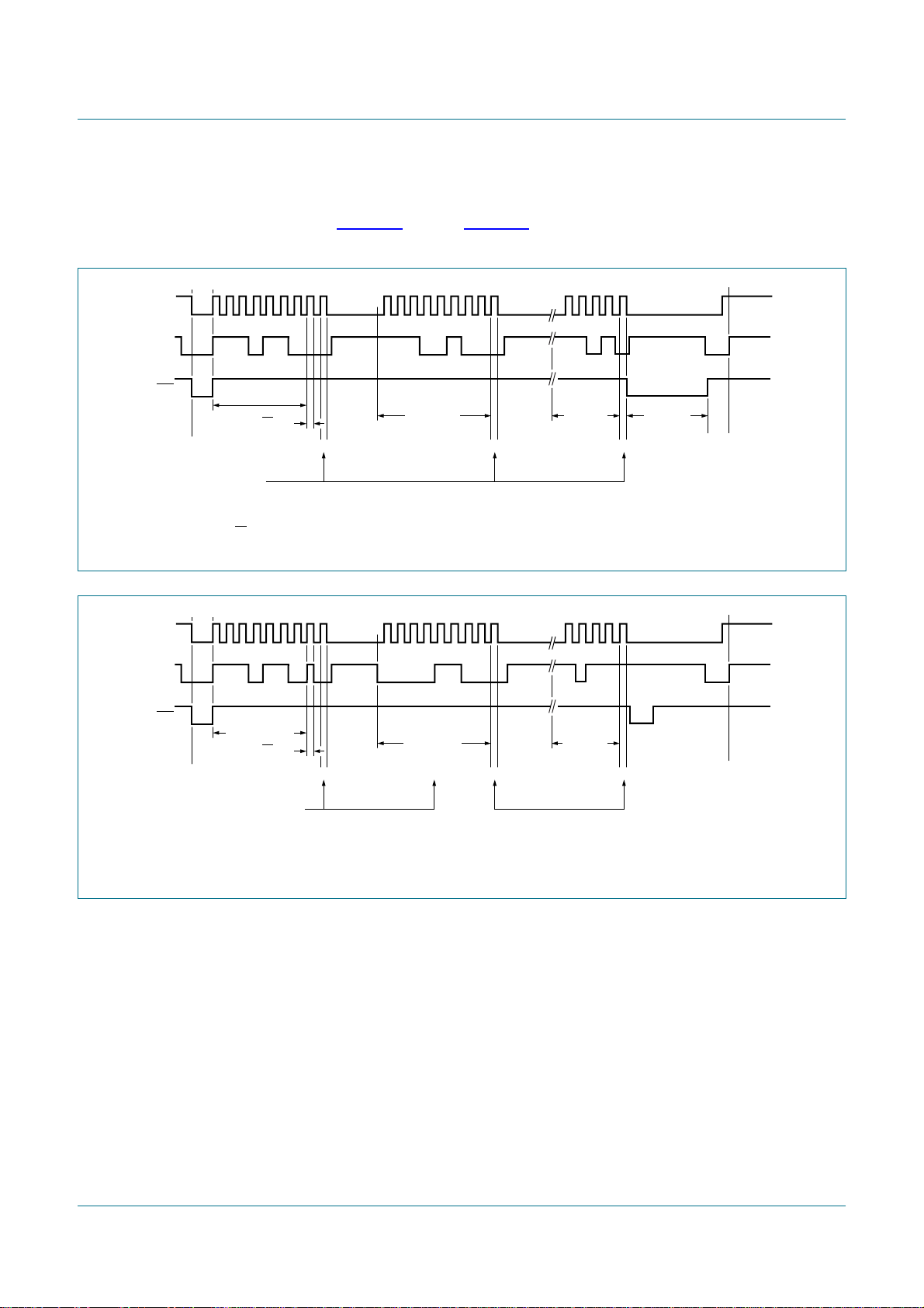
NXP Semiconductors
8.13 I2C-bus timing diagrams, Buffered mode
The diagrams (Figure 23 through Figure 26) illustrate typical timing diagrams for the
PCA9665 in master/slave functions.
SCL
SDA
PCA9665
Fm+ parallel bus to I2C-bus controller
INT
START
condition
from slave receiver
7-bit address
R/W = 0
(1)
n byte
(1)
interrupt
ACK
ACK
first byte
(1)
ACK
Master PCA9665 writes data to slave transmitter.
(1) 7-bit address + R/W = 0 byte and number of bytes sent = value programmed in I2CCOUNT register (BC[6:0] ≤ 68).
Fig 23. Bus timing diagram; Buffered Master Transmitter mode
SCL
SDA
INT
START
condition
7-bit address
R/W = 1
from slave
ACK
first byte
(1)
ACK
from master receiver
n byte
(1)
no ACK
STOP
condition
002aab267
STOP
condition
002aab268
Master PCA9665 reads data from slave transmitter.
(1) Number of bytes received = value programmed in I2CCOUNT register (BC[6:0]≤ 68).
Fig 24. Bus timing diagram; Buffered Master Receiver mode
PCA9665_2 © NXP B.V. 2006. All rights reserved.
Product data sheet Rev. 02 — 7 December 2006 63 of 91
Page 64

NXP Semiconductors
SCL
SDA
PCA9665
Fm+ parallel bus to I2C-bus controller
INT
START
condition
7-bit address
from slave PCA9665
R/W = 1
(1)
interrupt
ACK
first byte
(2)
ACK
from master receiver
External master receiver reads data from PCA9665.
(1) As defined in I2CADR register.
(2) Number of bytes received = value programmed in I2CCOUNT register (BC[6:0]≤ 68).
Fig 25. Bus timing diagram; Buffered Slave Transmitter mode
SCL
SDA
INT
START
condition
7-bit address
from slave PCA9665
R/W = 0
(1)
interrupt
ACK
first byte
(2)
ACK
n byte
n byte
(2)
(2)
no ACK
ACK
interrupt
interrupt
STOP
condition
002aab269
interrupt
(after STOP)
STOP
condition
002aab270
Slave PCA9665 is written to by external master transmitter.
(1) As defined in I2CADR register.
(2) Number of bytes received = value programmed in I2CCOUNT register (BC[6:0]≤ 68).
Fig 26. Bus timing diagram; Buffered Slave Receiver mode
SCL
SDA
INT
START
condition
7-bit SWRST
Call address
R/W = 0
from slave PCA9665
ACK
interrupt
first byte = 0xA5
ACK
second byte = 0x5A
ACK
interrupt
(after STOP)
STOP
condition
002aab488
Fig 27. Bus timing diagram; Software Reset Call
PCA9665_2 © NXP B.V. 2006. All rights reserved.
Product data sheet Rev. 02 — 7 December 2006 64 of 91
Page 65

NXP Semiconductors
9. Characteristics of the I2C-bus
The I2C-bus is for 2-way, 2-line communication between different ICs or modules. The two
lines are a serial data line (SDA) and a serial clock line (SCL). Both lines must be
connected to a positive supply via a pull-up resistor when connected to the output stages
of a device. Data transfer may be initiated only when the bus is not busy.
9.1 Bit transfer
One data bit is transferred during each clock pulse. The data on the SDA line must remain
stable during the HIGH period of the clock pulse as changes in the data line at this time
will be interpreted as control signals (see Figure 28).
SDA
SCL
PCA9665
Fm+ parallel bus to I2C-bus controller
Fig 28. Bit transfer
9.1.1 START and STOP conditions
Both data and clock lines remain HIGH when the bus is not busy. A HIGH-to-LOW
transition of the data line while the clock is HIGH is defined as the START condition (S). A
LOW-to-HIGH transition of the data line while the clock is HIGH is defined as the STOP
condition (P) (see Figure 29).
SDA
SCL
S
START condition
Fig 29. Definition of START and STOP conditions
9.2 System configuration
data line
stable;
data valid
change
of data
allowed
mba607
SDA
SCL
P
STOP condition
mba608
A device generating a message is a ‘transmitter’; a device receiving is the ‘receiver’. The
device that controls the message is the ‘master’ and the devices which are controlled by
the master are the ‘slaves’ (see Figure 30).
PCA9665_2 © NXP B.V. 2006. All rights reserved.
Product data sheet Rev. 02 — 7 December 2006 65 of 91
Page 66

NXP Semiconductors
SDA
SCL
PCA9665
Fm+ parallel bus to I2C-bus controller
MASTER
TRANSMITTER/
RECEIVER
Fig 30. System configuration
9.3 Acknowledge
The number of data bytes transferred between the START and the STOP conditions from
transmitter to receiver is not limited. Each byte of eight bits is followed by one
acknowledge bit. The acknowledge bit is a HIGH level put on the bus by the transmitter,
whereas the master generates an extra acknowledge related clock pulse.
A slave receiver which is addressed must generate an acknowledge after the reception of
each byte. Also a master must generate an acknowledge after the reception of each byte
that has been clocked out of the slave transmitter. The device that acknowledges has to
pull down the SDA line during the acknowledge clock pulse, so that the SDA line is stable
LOW during the HIGH period of the acknowledge related clock pulse; set-up and hold
times must be taken into account.
A master receiver must signal an end of data to the transmitter by not generating an
acknowledge on the last byte that has been clocked out of the slave. In this event, the
transmitter must leave the data line HIGH to enable the master to generate a STOP
condition.
SLAVE
RECEIVER
SLAVE
TRANSMITTER/
RECEIVER
MASTER
TRANSMITTER
MASTER
TRANSMITTER/
RECEIVER
SLAVE
I2C-BUS
MULTIPLEXER
002aaa966
data output
by transmitter
not acknowledge
data output
by receiver
acknowledge
SCL from master
S
START
condition
clock pulse for
acknowledgement
9821
002aaa987
Fig 31. Acknowledgement on the I2C-bus
PCA9665_2 © NXP B.V. 2006. All rights reserved.
Product data sheet Rev. 02 — 7 December 2006 66 of 91
Page 67
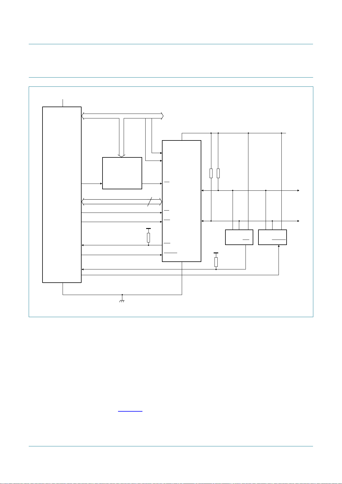
NXP Semiconductors
10. Application design-in information
V
DD
address bus
A0
A1
PCA9665
Fm+ parallel bus to I2C-bus controller
V
DD
V
DD
DECODER
ALE
80C51
V
SS
Fig 32. Application diagram using the 80C51
10.1 Specific applications
The PCA9665 is a parallel bus to I2C-bus controller that is designed to allow ‘smart’
devices to interface with I2C-bus or SMBus components, where the ‘smart’ device does
not have an integrated I2C-bus port and the designer does not want to ‘bit-bang’ the
I2C-bus port. The PCA9665 can also be used to add more I2C-bus ports to ‘smart’
devices, provide a higher frequency, lower voltage migration path for the PCF8584 and
convert 8 bits of parallel data to a serial bus to avoid running multiple traces across the
printed-circuit board.
PCA9665
CE
SCL
8
D0 to D7
RD
DD
WR
INT
RESET
V
SDA
SLAVE
INT RESET
V
DD
V
SS
SLAVE
002aab035
10.2 Add I2C-bus port
As shown in Figure 33, the PCA9665 converts 8-bits of parallel data into a multiple master
capable I2C-bus port for microcontrollers, microprocessors, custom ASICs, DSPs, etc.,
that need to interface with I2C-bus or SMBus components.
PCA9665_2 © NXP B.V. 2006. All rights reserved.
Product data sheet Rev. 02 — 7 December 2006 67 of 91
Page 68

NXP Semiconductors
PCA9665
Fm+ parallel bus to I2C-bus controller
MICROCONTROLLER,
MICROPROCESSOR,
OR ASIC
Fig 33. Adding I2C-bus port application
10.3 Add additional I2C-bus ports
The PCA9665 can be used to convert 8-bit parallel data into additional multiple master
capable I2C-bus port as shown in Figure 34. It is used if the microcontroller,
microprocessor, custom ASIC, DSP, etc., already have an I2C-bus port but need one or
more additional I2C-bus ports to interface with more I2C-bus or SMBus components or
components that cannot be located on the same bus (e.g., 100 kHz and 400 kHz slaves
on different buses so that each bus can operate at its maximum potential).
MICROCONTROLLER,
MICROPROCESSOR,
OR ASIC
control signals
8 bits data
SDA
SCL
control signals
8 bits data
PCA9665
SDA
SCL
002aab036
SDA
PCA9665
SCL
002aab037
Fig 34. Adding additional I2C-bus ports application
10.4 Convert 8 bits of parallel data into I2C-bus serial data stream
Functioning as a slave transmitter, the PCA9665 can convert 8-bit parallel data into a
two-wire I2C-bus data stream as is shown in Figure 35. This would prevent having to run
8 traces across the entire width of the printed-circuit board.
MICROCONTROLLER,
MICROPROCESSOR,
OR ASIC
control signals
PCA9665
8 bits data
Fig 35. Converting parallel to serial data application
SDA
SCL
MASTER
002aab039
PCA9665_2 © NXP B.V. 2006. All rights reserved.
Product data sheet Rev. 02 — 7 December 2006 68 of 91
Page 69

NXP Semiconductors
PCA9665
Fm+ parallel bus to I2C-bus controller
11. Limiting values
Table 47. Limiting values
In accordance with the Absolute Maximum Rating System (IEC 60134).
Symbol Parameter Conditions Min Max Unit
V
DD
V
I
I
I
I
O
P
tot
P/out power dissipation per output - 50 mW
T
stg
T
amb
[1] 5.5 V steady state voltage tolerance on inputs and outputs is valid only when the supply voltage is present. 4.6 V steady state voltage
tolerance on inputs and outputs when no supply voltage is present.
supply voltage −0.3 +4.6 V
input voltage any input
[1]
−0.8 +6.0 V
input current any input −10 +10 mA
output current any output −10 +10 mA
total power dissipation - 300 mW
storage temperature −65 +150 °C
ambient temperature operating −40 +85 °C
PCA9665_2 © NXP B.V. 2006. All rights reserved.
Product data sheet Rev. 02 — 7 December 2006 69 of 91
Page 70

NXP Semiconductors
PCA9665
Fm+ parallel bus to I2C-bus controller
12. Static characteristics
Table 48. Static characteristics
VDD = 2.3 V to 3.6 V; T
Symbol Parameter Conditions Min Typ Max Unit
Supply
V
DD
I
DD
V
POR
Inputs
V
IL
V
IH
I
L
C
i
supply voltage 2.3 - 3.6 V
supply current standby mode - 0.1 3.0 mA
power-on reset voltage - 1.8 2.2 V
WR, RD, A0, A1, CE, RESET
LOW-level input voltage 0 - 0.8 V
HIGH-level input voltage
leakage current input; VI= 0 V or 5.5 V −1-+1µA
input capacitance VI=VSS or V
Inputs/outputs D0 to D7
V
V
I
I
I
C
IL
IH
OH
OL
L
io
LOW-level input voltage 0 - 0.8 V
HIGH-level input voltage
HIGH-level output current VOH=VDD− 0.4 V −4.0 −7.0 - mA
LOW-level output current VOL= 0.4 V 4.0 8.0 - mA
leakage current input; VI= 0 V or 5.5 V −1-+1µA
input/output capacitance VI=VSS or V
SDA and SCL
V
IL
V
IH
I
L
I
OL
C
io
Outputs
I
OL
I
L
C
o
LOW-level input voltage 0 - 0.3V
HIGH-level input voltage
leakage current input/output; VI= 0 V or 3.6 V −1-+1µA
LOW-level output current VOL= 0.4 V 20 - - mA
input/output capacitance VI=VSS or V
INT
LOW-level output current VOL= 0.4 V 6.0 - - mA
leakage current VO= 0 V or 3.6 V −1-+1µA
output capacitance VI=VSS or V
=−40°C to +85°C; unless otherwise specified.
amb
operating mode; no load - - 8.0 mA
DD
DD
input/output; V
= 5.5 V −1 - +10 µA
I
DD
DD
[1]
2.0 - 5.5 V
- 2.0 3 pF
[1]
2.0 - 5.5 V
- 2.8 4 pF
DD
[1]
0.7V
- 5.5 V
DD
- 5.6 7 pF
- 3.8 5 pF
V
[1] 5.5 V steady state voltage tolerance on inputs and outputs is valid only when the supply voltage is present. 4.6 V steady state voltage
tolerance on inputs and outputs when no supply voltage is present.
PCA9665_2 © NXP B.V. 2006. All rights reserved.
Product data sheet Rev. 02 — 7 December 2006 70 of 91
Page 71

NXP Semiconductors
13. Dynamic characteristics
PCA9665
Fm+ parallel bus to I2C-bus controller
Table 49. Dynamic characteristics (3.3 volt)
VCC= 3.3 V±0.3 V; T
=−40°C to +85°C; unless otherwise specified. (See Table50 on page 72 for 2.5 V)
amb
[1][2][3]
Symbol Parameter Conditions Min Typ Max Unit
Initialization timing
t
init(po)
power-on initialization time - - 550 µs
Serial interface initialization timing
t
init(sintf)
serial interface initialization time
[4]
from ENSIO bit HIGH - - 550 µs
RESET timing (see Figure 36)
t
w(rst)
t
rst
t
rec(rst)
reset pulse width 10 - - ns
reset time
[5][6]
250 - - ns
reset recovery time 0 - - ns
INT timing (see Figure 37)
t
as(int)
t
das(int)
Bus timing (see
t
su(A)
t
h(A)
t
su(CE_N)
t
h(CE_N)
t
w(RDL)
t
w(WRL)
t
d(DV)
t
d(QZ)
t
su(Q)
t
h(Q)
t
w(RDH)
t
w(WRH)
interrupt assert time - - 500 ns
interrupt de-assert time - - 20 ns
Figure 38 and Figure 40)
address setup time to RD, WR LOW 0 - - ns
address hold time from RD, WR LOW 13 - - ns
CE setup time to RD, WR LOW 0 - - ns
CE hold time from RD, WR LOW 0 - - ns
RD LOW pulse width 20 - - ns
WR LOW pulse width 20 - - ns
data valid delay time after RD and CE LOW - - 17 ns
data output float delay time after RD or CE HIGH - - 17 ns
data output setup time beforeWR or CE HIGH (write cycle) 12 - - ns
data output hold time after WR HIGH 0 - - ns
RD HIGH pulse width 18 - - ns
WR HIGH pulse width 18 - - ns
[1] Parameters are valid over specified temperature and voltage range.
[2] All voltage measurements are referenced to ground (GND). For testing, all inputs swing between 0 V and 3.0 V with a transition time of
5 ns maximum. All time measurements are referenced at input voltages of 1.5 V and output voltages shown in Figure 38 and Figure 40.
[3] Test conditions for outputs: CL= 50 pF; RL= 500 Ω, except open-drain outputs.
Test conditions for open-drain outputs: CL= 50 pF; RL=1kΩ pull-up to VDD.
[4] Initialization time for the serial interface after ENSIO bit goes HIGH in a write operation to the control register.
[5] Resetting the device while actively communicating on the bus may cause glitches or an errant STOP condition.
[6] Upon reset, the full delay will be the sum of t
PCA9665_2 © NXP B.V. 2006. All rights reserved.
Product data sheet Rev. 02 — 7 December 2006 71 of 91
and the RC time constant of the SDA and SCL bus.
rst
Page 72

NXP Semiconductors
PCA9665
Fm+ parallel bus to I2C-bus controller
Table 50. Dynamic characteristics (2.5 volt)
VCC= 2.5 V±0.2 V; T
=−40°C to +85°C; unless otherwise specified. (See Table49 on page 71 for 3.3 V)
amb
[1][2][3]
Symbol Parameter Conditions Min Typ Max Unit
Initialization timing
t
init(po)
power-on initialization time - - 550 µs
Serial interface initialization timing
t
init(sintf)
serial interface initialization time
[4]
from ENSIO bit HIGH - - 550 µs
RESET timing (see Figure 36)
t
w(rst)
t
rst
t
rec(rst)
reset pulse width 10 - - ns
reset time
[5][6]
250 - - ns
reset recovery time 0 - - ns
INT timing (see Figure 37)
t
as(int)
t
das(int)
Bus timing (see
t
su(A)
t
h(A)
t
su(CE_N)
t
h(CE_N)
t
w(RDL)
t
w(WRL)
t
d(DV)
t
d(QZ)
t
su(Q)
t
h(Q)
t
w(RDH)
t
w(WRH)
interrupt assert time - - 550 ns
interrupt de-assert time - - 20 ns
Figure 38 and Figure 40)
address setup time to RD, WR LOW 0 - - ns
address hold time from RD, WR LOW 13 - - ns
CE setup time to RD, WR LOW 0 - - ns
CE hold time from RD, WR LOW 0 - - ns
RD LOW pulse width 20 - - ns
WR LOW pulse width 20 - - ns
data valid delay time after RD and CE LOW - - 22 ns
data output float delay time after RD or CE HIGH - - 17 ns
data output setup time beforeWR or CE HIGH (write cycle) 12 - - ns
data output hold time after WR HIGH 0 - - ns
RD HIGH pulse width 18 - - ns
WR HIGH pulse width 18 - - ns
[1] Parameters are valid over specified temperature and voltage range.
[2] All voltage measurements are referenced to ground (GND). For testing, all inputs swing between 0 V and 3.0 V with a transition time of
5 ns maximum. All time measurements are referenced at input voltages of 1.5 V and output voltages shown in Figure 38 and Figure 40.
[3] Test conditions for outputs: CL= 50 pF; RL= 500 Ω, except open-drain outputs.
Test conditions for open-drain outputs: CL= 50 pF; RL=1kΩ pull-up to VDD.
[4] Initialization time for the serial interface after ENSIO bit goes HIGH in a write operation to the control register.
[5] Resetting the device while actively communicating on the bus may cause glitches or an errant STOP condition.
[6] Upon reset, the full delay will be the sum of t
PCA9665_2 © NXP B.V. 2006. All rights reserved.
Product data sheet Rev. 02 — 7 December 2006 72 of 91
and the RC time constant of the SDA and SCL bus.
rst
Page 73

NXP Semiconductors
PCA9665
Fm+ parallel bus to I2C-bus controller
SCL
SDA
RESET
Dn
Fig 36. Reset timing
50 %
t
rec(rst)
D7 to D0
START
WR
30 %
ACK or read cycle
t
rst
50 % 50 %
t
w(rst)
t
rst
Dn on
write to I2CCON
30 %
30 %
30 %
Dn off
002aab272
6789
SCL
INT
Fig 37. Interrupt timing
t
as(int)
t
das(int)
123
002aac227
PCA9665_2 © NXP B.V. 2006. All rights reserved.
Product data sheet Rev. 02 — 7 December 2006 73 of 91
Page 74
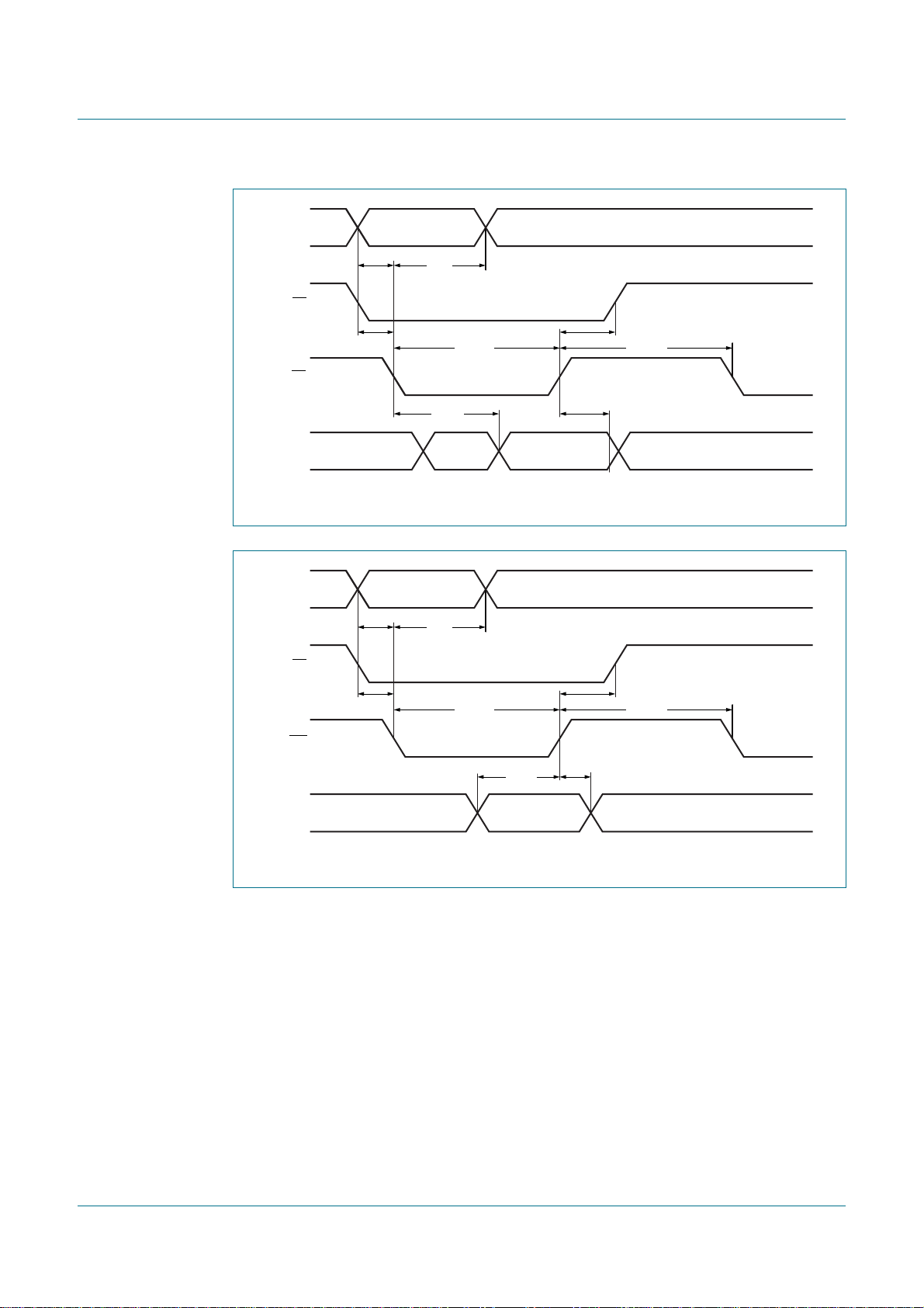
NXP Semiconductors
A0 to A1
CE
t
su(A)
t
h(A)
PCA9665
Fm+ parallel bus to I2C-bus controller
t
su(CE_N)
RD
D0 to D7
(read)
float floatnot valid valid
Fig 38. Bus timing (read cycle)
A0 to A1
t
su(A)
CE
WR
t
su(CE_N)
t
h(A)
t
d(DV)
t
w(RDL)
t
w(WRL)
t
su(Q)
t
h(Q)
t
d(QZ)
t
h(CE_N)
t
w(RDH)
t
h(CE_N)
t
w(WRH)
002aac693
D0 to D7
(write)
valid
002aac692
Fig 39. Parallel bus timing (write cycle)
PCA9665_2 © NXP B.V. 2006. All rights reserved.
Product data sheet Rev. 02 — 7 December 2006 74 of 91
Page 75

NXP Semiconductors
Fig 40. Data timing
Fm+ parallel bus to I2C-bus controller
V
I
RD, CE input
GND
V
Dn output
LOW-to-float
float-to-LOW
Dn output
HIGH-to-float
float-to-HIGH
DD
V
OL
V
OH
GND
VM= 1.5 V
VX=VOL+ 0.3 V
VY=VOH− 0.3 V
VOL and VOH are typical output voltage drops that occur with the output load.
V
M
t
d(QLZ)
t
d(QHZ)
outputs
enabled
V
M
t
d(QZL)
V
M
V
X
t
d(QZH)
V
Y
V
outputs
floating
PCA9665
M
outputs
enabled
002aab274
PCA9665_2 © NXP B.V. 2006. All rights reserved.
Product data sheet Rev. 02 — 7 December 2006 75 of 91
Page 76

NXP Semiconductors
PCA9665
Fm+ parallel bus to I2C-bus controller
Table 51. I2C-bus frequency and timing specifications
All the timing limits are valid within the operating supply voltage and ambient temperature range; VDD= 2.5 V±0.2 V and
3.3 V
±
0.3 V; T
Symbol Parameter Conditions Standard-mode
f
SCL
t
BUF
SCL clock frequency
bus free time between a
STOP and START
condition
t
HD;STA
hold time (repeated)
START condition
t
SU;STA
set-up time for a
repeated START
condition
t
SU;STO
set-up time for STOP
condition
t
HD;DAT
t
VD;ACK
data hold time 0 - 0 - 0 - ns
data valid acknowledge
time
t
VD;DAT
t
SU;DAT
t
LOW
data valid time
data set-up time 250 - 100 - 50 - ns
LOW period of the SCL
clock
t
HIGH
HIGH period of the SCL
clock
t
f
fall time of both SDA and
SCL signals
t
r
rise time of both SDAand
SCL signals
t
SP
pulse width of spikes that
must be suppressed by
the input filter
=−40°C to +85°C; and refer to VIL and VIH with an input voltage of VSS to VDD.
amb
Fast-mode I2C-bus Fast-modePlus
2
I
C-bus
Min Max Min Max Min Max
[1]
0 100 0 400 0 1000 kHz
4.7 - 1.3 - 0.5 - µs
4.0 - 0.6 - 0.26 - µs
4.7 - 0.6 - 0.26 - µs
4.0 - 0.6 - 0.26 - µs
[2]
0.05 3.45 0.05 0.9 0.05 0.45 µs
[3]
50 - 50 - 50 - ns
4.7 - 1.3 - 0.5 - µs
4.0 - 0.6 - 0.26 - µs
[5][6]
- 300 20 + 0.1C
- 1000 20 + 0.1C
[7]
- 50 - 50 - 50 ns
[4]
b
[4]
b
2
I
C-bus
300 - 120 ns
300 - 120 ns
Unit
[1] Minimum SCL clock frequency is limited by the bus time-out feature, which resets the serial bus interface if either SDA or SCL is held
LOW for a minimum of 25ms. Disable bus time-out feature for DC operation.
[2] t
[3] t
[4] Cb= total capacitance of one bus line in pF.
[5] A master device must internally provide a hold time of at least 300 ns for the SDA signal (refer to the VIL of the SCL signal) in order to
[6] The maximum tf for the SDA and SCL bus lines is specified at 300 ns. The maximum fall time for the SDA output stage tf is specified at
[7] Input filters on the SDA and SCL inputs suppress noise spikes less than 50 ns.
PCA9665_2 © NXP B.V. 2006. All rights reserved.
Product data sheet Rev. 02 — 7 December 2006 76 of 91
= time for Acknowledgement signal from SCL LOW to SDA (out) LOW.
VD;ACK
= minimum time for SDA data out to be valid following SCL LOW.
VD;DAT
bridge the undefined region SCL’s falling edge.
250 ns. This allows series protection resistors to be connected between the SDA and the SCL pins and the SDA/SCL bus lines without
exceeding the maximum specified tf.
Page 77
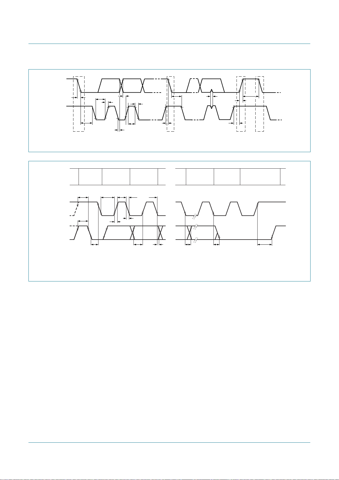
NXP Semiconductors
SDA
t
t
f
SCL
S
Fig 41. Definition of timing on the I2C-bus
LOW
t
HD;STA
t
r
t
t
HD;DAT
SU;DAT
t
HIGH
t
f
t
SU;STA
PCA9665
Fm+ parallel bus to I2C-bus controller
t
t
HD;STA
t
SP
t
SU;STO
Sr
t
r
P S
BUF
002aab271
protocol
START
condition
(S)
t
SU;STA
SCL
t
BUF
SDA
t
HD;STA
Rise and fall times refer to VIL and VIH.
Fig 42. I2C-bus timing diagram
bit 7
MSB
t
LOWtHIGH
t
r
bit 6 bit n bit 0
1
/f
SCL
t
f
t
SU;DAT
t
HD;DAT
t
VD;DAT
acknowledge
t
VD;ACK
(A)
STOP
condition
(P)
t
SU;STO
002aac696
PCA9665_2 © NXP B.V. 2006. All rights reserved.
Product data sheet Rev. 02 — 7 December 2006 77 of 91
Page 78
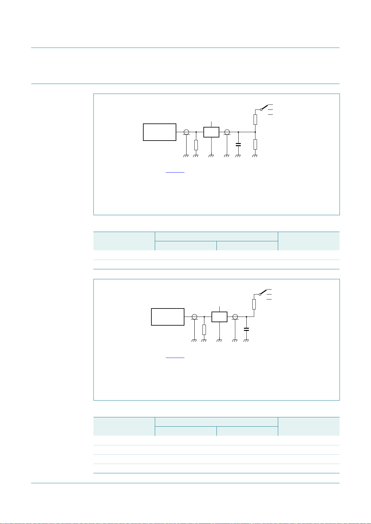
NXP Semiconductors
14. Test information
Fig 43. Test circuitry for switching times
PCA9665
Fm+ parallel bus to I2C-bus controller
VDD × 2
open
V
L
L
SS
002aac694
PULSE
GENERATOR
V
DD
DUT
V
O
V
I
R
T
C
L
50 pF
R
500 Ω
R
500 Ω
Test data are given in Table 52.
RL= load resistance.
CL= load capacitance includes jig and probe capacitance.
RT= termination resistance should be equal to the output impedance ZO of the pulse
generators.
Table 52. Test data
Test Load S1
t
d(DV)
t
d(QZ)
C
L
50 pF 500 Ω VDD× 2
50 pF 500 Ω open
V
PULSE
GENERATOR
Test data are given in Table 53.
RL= load resistance. RL for SDA and SCL> 1 kΩ (3 mA or less current).
CL= load capacitance includes jig and probe capacitance.
RT= termination resistance should be equal to the output impedance ZO of the pulse
generators.
I
R
L
V
DD
open
V
V
DD
V
DUT
R
T
O
C
L
50 pF
R
L
1 kΩ
002aac695
SS
Fig 44. Test circuitry for open-drain switching times
Table 53. Test data
Test Load S1
C
L
t
d(DV)
t
d(QZ)
t
as(int)
t
das(int)
PCA9665_2 © NXP B.V. 2006. All rights reserved.
50 pF 1 kΩ V
50 pF 1 kΩ V
50 pF 1 kΩ V
50 pF 1 kΩ V
Product data sheet Rev. 02 — 7 December 2006 78 of 91
R
L
DD
DD
DD
DD
Page 79
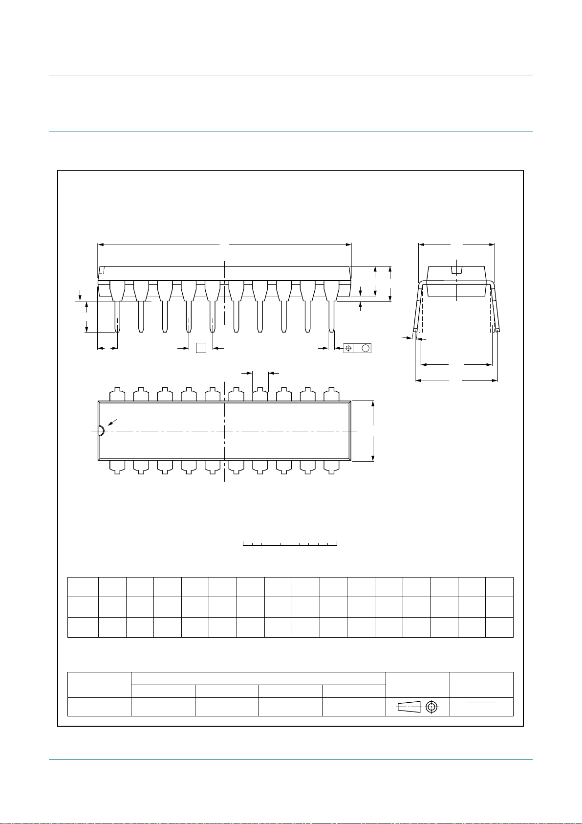
NXP Semiconductors
15. Package outline
PCA9665
Fm+ parallel bus to I2C-bus controller
DIP20: plastic dual in-line package; 20 leads (300 mil)
D
seating plane
L
Z
20
pin 1 index
e
b
SOT146-1
M
E
A
2
A
A
1
w M
b
1
11
E
c
(e )
1
M
H
1
0 5 10 mm
scale
DIMENSIONS (inch dimensions are derived from the original mm dimensions)
A
UNIT
mm
inches
Note
1. Plastic or metal protrusions of 0.25 mm (0.01 inch) maximum per side are not included.
max.
OUTLINE
VERSION
SOT146-1
A
min.
A
1 2
max.
IEC JEDEC JEITA
b
1.73
1.30
0.068
0.051
b
0.53
0.38
0.021
0.015
1
cD E e M
0.36
0.23
0.014
0.009
REFERENCES
(1) (1)
26.92
26.54
1.060
1.045
SC-603MS-001
6.40
6.22
0.25
0.24
10
(1)
1
3.60
8.25
3.05
7.80
0.14
0.32
0.12
0.31
EUROPEAN
PROJECTION
H
E
10.0
0.2542.54 7.62
8.3
0.39
0.010.1 0.3
0.33
ISSUE DATE
M
L
e
w
99-12-27
03-02-13
Z
max.
24.2 0.51 3.2
0.0780.17 0.02 0.13
Fig 45. Package outline SOT146-1 (DIP20)
PCA9665_2 © NXP B.V. 2006. All rights reserved.
Product data sheet Rev. 02 — 7 December 2006 79 of 91
Page 80

NXP Semiconductors
PCA9665
Fm+ parallel bus to I2C-bus controller
SO20: plastic small outline package; 20 leads; body width 7.5 mm
D
c
y
Z
20
pin 1 index
1
e
11
A
2
10
w M
b
p
SOT163-1
E
H
E
Q
A
1
L
p
L
detail X
(A )
A
X
v M
A
A
3
θ
0 5 10 mm
scale
DIMENSIONS (inch dimensions are derived from the original mm dimensions)
mm
OUTLINE
VERSION
SOT163-1
A
A1A2A3b
max.
0.3
2.65
0.1
0.012
0.1
0.004
p
2.45
2.25
0.096
0.089
IEC JEDEC JEITA
075E04 MS-013
0.25
0.01
0.49
0.36
0.019
0.014
0.32
0.23
0.013
0.009
UNIT
inches
Note
1. Plastic or metal protrusions of 0.15 mm (0.006 inch) maximum per side are not included.
(1)E(1) (1)
cD
13.0
12.6
0.51
0.49
REFERENCES
eHELLpQ
7.6
7.4
0.30
0.29
1.27
0.05
10.65
10.00
0.419
0.394
1.4
0.055
1.1
0.4
0.043
0.016
1.1
1.0
0.043
0.039
0.25
0.25 0.1
0.01
0.01
EUROPEAN
PROJECTION
ywv θ
Z
0.9
0.4
0.035
0.004
0.016
ISSUE DATE
99-12-27
03-02-19
o
8
o
0
Fig 46. Package outline SOT163-1 (SO20)
PCA9665_2 © NXP B.V. 2006. All rights reserved.
Product data sheet Rev. 02 — 7 December 2006 80 of 91
Page 81

NXP Semiconductors
PCA9665
Fm+ parallel bus to I2C-bus controller
TSSOP20: plastic thin shrink small outline package; 20 leads; body width 4.4 mm
D
c
y
Z
20
pin 1 index
11
A
2
A
1
110
w M
b
e
p
E
H
E
L
detail X
SOT360-1
A
X
v M
A
Q
(A )
3
A
θ
L
p
0 2.5 5 mm
scale
DIMENSIONS (mm are the original dimensions)
UNIT A1A2A
Notes
1. Plastic or metal protrusions of 0.15 mm maximum per side are not included.
2. Plastic interlead protrusions of 0.25 mm maximum per side are not included.
A
max.
0.15
mm
1.1
OUTLINE
VERSION
SOT360-1 MO-153
0.05
0.95
0.80
IEC JEDEC JEITA
0.25
b
3
p
0.30
0.19
(1)E(2) (1)
cD
0.2
6.6
0.1
6.4
REFERENCES
eHELLpQZywv θ
4.5
4.3
0.65
6.6
6.2
0.75
0.50
0.4
0.3
EUROPEAN
PROJECTION
o
0.5
0.13 0.10.21
ISSUE DATE
99-12-27
03-02-19
0.2
8
o
0
Fig 47. Package outline SOT360-1 (TSSOP20)
PCA9665_2 © NXP B.V. 2006. All rights reserved.
Product data sheet Rev. 02 — 7 December 2006 81 of 91
Page 82

NXP Semiconductors
HVQFN20: plastic thermal enhanced very thin quad flat package; no leads;
20 terminals; body 5 x 5 x 0.85 mm
A
D
terminal 1
index area
B
E
PCA9665
Fm+ parallel bus to I2C-bus controller
SOT662-1
A
A
1
detail X
c
e
1
e
L
5
E
h
1
terminal 1
index area
DIMENSIONS (mm are the original dimensions)
(1)
A
UNIT
mm
Note
1. Plastic or metal protrusions of 0.075 mm maximum per side are not included.
OUTLINE
VERSION
SOT662-1 MO-220- - - - - -
max.
A
0.05
0.00
1
0.38
0.23
610
20
(1)
c
b
D
5.1
0.2
4.9
IEC JEDEC JEITA
b
11
e
15
D
D
3.25
2.95
16
h
0 2.5 5 mm
scale
(1)
E
E
h
h
5.1
3.25
4.9
2.95
REFERENCES
0.651
v
w
2.6
C
M
ACCB
M
e
2
e
e
2.6
L
2
0.75
0.50
1
y
C
1
w
0.1v0.05
ye
0.05 0.1
EUROPEAN
PROJECTION
y
X
y
1
ISSUE DATE
01-08-08
02-10-22
Fig 48. Package outline SOT662-1 (HVQFN20)
PCA9665_2 © NXP B.V. 2006. All rights reserved.
Product data sheet Rev. 02 — 7 December 2006 82 of 91
Page 83

NXP Semiconductors
16. Handling information
Inputs and outputs are protected against electrostatic discharge in normal handling.
However, to be completely safe you must take normal precautions appropriate to handling
integrated circuits.
17. Soldering
17.1 Introduction
There is no soldering method that is ideal for all surface mount IC packages. Wave
soldering can still be used for certain surface mount ICs, but it is not suitable for fine pitch
SMDs. In these situations reflow soldering is recommended.
17.2 Through-hole mount packages
17.2.1 Soldering by dipping or by solder wave
Typical dwell time of the leads in the wave ranges from 3 seconds to 4 seconds at 250 °C
or 265 °C, depending on solder material applied, SnPb or Pb-free respectively.
PCA9665
Fm+ parallel bus to I2C-bus controller
The total contact time of successive solder waves must not exceed 5 seconds.
The device may be mounted up to the seating plane, but the temperature of the plastic
body must not exceed the specified maximum storage temperature (T
printed-circuit board has been pre-heated, forced cooling may be necessary immediately
after soldering to keep the temperature within the permissible limit.
17.2.2 Manual soldering
Apply the soldering iron (24 V or less) to the lead(s) of the package, either below the
seating plane or not more than 2 mm above it. If the temperature of the soldering iron bit is
less than 300 °C it may remain in contact for up to 10 seconds. If the bit temperature is
between 300 °C and 400 °C, contact may be up to 5 seconds.
17.3 Surface mount packages
17.3.1 Reflow soldering
Key characteristics in reflow soldering are:
• Lead-free versus SnPb soldering; note that a lead-free reflow process usually leads to
higher minimum peak temperatures (see Figure 49) than a PbSn process, thus
reducing the process window
• Solder paste printing issues including smearing, release, and adjusting the process
window for a mix of large and small components on one board
• Reflow temperature profile; this profile includes preheat, reflow (in which the board is
heated to the peak temperature) and cooling down. It is imperative that the peak
temperature is high enough for the solder to make reliable solder joints (a solder paste
characteristic). In addition, the peak temperature must be low enough that the
stg(max)
). If the
PCA9665_2 © NXP B.V. 2006. All rights reserved.
Product data sheet Rev. 02 — 7 December 2006 83 of 91
Page 84

NXP Semiconductors
Table 54. SnPb eutectic process (from J-STD-020C)
Package thickness (mm) Package reflow temperature (°C)
< 2.5 235 220
≥ 2.5 220 220
Table 55. Lead-free process (from J-STD-020C)
Package thickness (mm) Package reflow temperature (°C)
< 1.6 260 260 260
1.6 to 2.5 260 250 245
> 2.5 250 245 245
PCA9665
Fm+ parallel bus to I2C-bus controller
packages and/or boards are not damaged. The peak temperature of the package
depends on package thickness and volume and is classified in accordance with
Table 54 and 55
Volume (mm3)
< 350 ≥ 350
Volume (mm3)
< 350 350 to 2000 > 2000
Moisture sensitivity precautions, as indicated on the packing, must be respected at all
times.
Studies have shown that small packages reach higher temperatures during reflow
soldering, see Figure 49.
maximum peak temperature
temperature
MSL: Moisture Sensitivity Level
Fig 49. Temperature profiles for large and small components
= MSL limit, damage level
minimum peak temperature
= minimum soldering temperature
peak
temperature
time
001aac844
For further information on temperature profiles, refer to Application Note
“Surface mount reflow soldering description”
PCA9665_2 © NXP B.V. 2006. All rights reserved.
Product data sheet Rev. 02 — 7 December 2006 84 of 91
.
AN10365
Page 85

NXP Semiconductors
17.3.2 Wave soldering
Conventional single wave soldering is not recommended for surface mount devices
(SMDs) or printed-circuit boards with a high component density, as solder bridging and
non-wetting can present major problems.
To overcome these problems the double-wave soldering method was specifically
developed.
If wave soldering is used the following conditions must be observed for optimal results:
• Use a double-wave soldering method comprising a turbulent wave with high upward
• For packages with leads on two sides and a pitch (e):
• For packages with leads on four sides, the footprint must be placed at a 45° angle to
PCA9665
Fm+ parallel bus to I2C-bus controller
pressure followed by a smooth laminar wave.
– larger than or equal to 1.27 mm, the footprint longitudinal axis is preferred to be
parallel to the transport direction of the printed-circuit board;
– smaller than 1.27 mm, the footprint longitudinal axis must be parallel to the
transport direction of the printed-circuit board.
The footprint must incorporate solder thieves at the downstream end.
the transport direction of the printed-circuit board. The footprint must incorporate
solder thieves downstream and at the side corners.
During placement and before soldering, the package must be fixed with a droplet of
adhesive. The adhesive can be applied by screen printing, pin transfer or syringe
dispensing. The package can be soldered after the adhesive is cured.
Typical dwell time of the leads in the wave ranges from 3 seconds to 4 seconds at 250 °C
or 265 °C, depending on solder material applied, SnPb or Pb-free respectively.
A mildly-activated flux will eliminate the need for removal of corrosive residues in most
applications.
17.3.3 Manual soldering
Fix the component by first soldering two diagonally-opposite end leads. Use a low voltage
(24 V or less) soldering iron applied to the flat part of the lead. Contact time must be
limited to 10 seconds at up to 300 °C.
When using a dedicated tool, all other leads can be soldered in one operation within
2 seconds to 5 seconds between 270 °C and 320 °C.
17.4 Package related soldering information
Table 56. Suitability of IC packages for wave, reflow and dipping soldering methods
Mounting Package
Through-hole mount CPGA, HCPGA suitable −−
DBS, DIP, HDIP, RDBS, SDIP, SIL suitable
Through-hole-surface
mount
PMFP
[1]
[4]
Soldering method
Wave Reflow
[3]
not suitable not suitable −
[2]
− suitable
Dipping
PCA9665_2 © NXP B.V. 2006. All rights reserved.
Product data sheet Rev. 02 — 7 December 2006 85 of 91
Page 86

NXP Semiconductors
PCA9665
Fm+ parallel bus to I2C-bus controller
Table 56. Suitability of IC packages for wave, reflow and dipping soldering methods
Mounting Package
[1]
Soldering method
Wave Reflow
Surface mount BGA, HTSSON..T
LFBGA,SQFP,SSOP..T
[5]
, LBGA,
[5]
,TFBGA,
not suitable suitable −
…continued
[2]
Dipping
VFBGA, XSON
DHVQFN, HBCC, HBGA, HLQFP,
not suitable
[6]
suitable −
HSO, HSOP, HSQFP, HSSON,
HTQFP, HTSSOP, HVQFN,
HVSON, SMS
[7]
PLCC
LQFP, QFP, TQFP not recommended
SSOP, TSSOP, VSO, VSSOP not recommended
CWQCCN..L
[1] For more detailed information on the BGA packages refer to the
Semiconductors sales office.
[2] All surface mount (SMD) packages are moisture sensitive. Depending upon the moisture content, the maximum temperature (with
respect to time) and body size of the package, there is a risk that internal or external package cracks may occur due to vaporization of
the moisture in them (the so called popcorn effect).
[3] For SDIP packages, the longitudinal axis must be parallel to the transport direction of the printed-circuit board.
[4] Hot bar soldering or manual soldering is suitable for PMFP packages.
[5] These transparent plastic packages are extremely sensitive to reflow soldering conditions and must on no account be processed
through more than one soldering cycle or subjected to infrared reflow soldering with peak temperature exceeding 217 °C ± 10 °C
measured in the atmosphere of the reflow oven. The package body peak temperature must be kept as low as possible.
[6] These packages are not suitable for wave soldering. On versions with the heatsink on the bottom side, the solder cannot penetrate
between the printed-circuit board and the heatsink. On versions with the heatsink on the top side, the solder might be deposited on the
heatsink surface.
[7] If wave soldering is considered, then the package must be placed at a 45° angle to the solder wave direction. The package footprint
must incorporate solder thieves downstream and at the side corners.
[8] Wave soldering is suitable for LQFP, QFP and TQFP packages with a pitch (e) larger than 0.8 mm; it is definitely not suitable for
packages with a pitch (e) equal to or smaller than 0.65 mm.
[9] Wave soldering is suitable for SSOP, TSSOP, VSO and VSSOP packages with a pitch (e) equal to or larger than 0.65 mm; it is definitely
not suitable for packages with a pitch (e) equal to or smaller than 0.5mm.
[10] Image sensor packages in principle should not be soldered. They are mounted in sockets or delivered pre-mounted on flex foil.
However, the image sensor package can be mounted by the client on a flex foil by using a hot bar soldering process. The appropriate
soldering profile can be provided on request.
, SO, SOJ suitable suitable −
[10]
, WQCCN..L
[10]
not suitable not suitable −
(LF)BGA Application Note
[7][8]
[9]
(AN01026); order a copy from your NXP
suitable −
suitable −
PCA9665_2 © NXP B.V. 2006. All rights reserved.
Product data sheet Rev. 02 — 7 December 2006 86 of 91
Page 87

NXP Semiconductors
18. Abbreviations
Table 57. Abbreviations
Acronym Description
ASIC Application Specific Integrated Circuit
CDM Charged Device Model
CPU Central Processing Unit
DSP Digital Signal Processing
ESD ElectroStatic Discharge
HBM Human Body Model
2
C-bus Inter-Integrated Circuit bus
I
I/O Input/Output
MM Machine Model
PCB Printed-Circuit Board
SMBus System Management Bus
PCA9665
Fm+ parallel bus to I2C-bus controller
19. Revision history
Table 58. Revision history
Document ID Release date Data sheet status Change notice Supersedes
PCA9665_2 20061207 Product data sheet - PCA9665_1
Modifications:
• The format of this data sheet has been redesigned to comply with the new identity guidelines of NXP
Semiconductors.
• Legal texts have been adapted to the new company name where appropriate.
• Descriptive title changed from “Fast-modePlus parallel bus to I
2
to I
C-bus controller”
• Table 12 “I2CCON - Control register (A1 = 1, A0 = 1) bit description”, description of bit 6, 4
paragraph: changed “... it takes 550 µs for the internal oscillator to start up, ...” to “... it takes 550 µs
enable time for the internal oscillator to start up, and the serial interface to initialize.”
• Table 25 “I
position revised
2
C-bus mode selection example
[1]
”, Table note2: equation denominator close parenthesis
2
C-bus controller” to “Fm+ parallel bus
th
• Table 48 “Static characteristics”:
– sub-section “Supply”: unit for I
– sub-section “Supply”: I
– sub-section “Inputs
– sub-section “Inputs/outputs D0 to D7”, C
– sub-section “SDA and SCL”, C
7pF
– sub-section “Outputs
5pF
DD
WR, RD, A0, A1, CE, RESET”, Ci (Typ) changed from 1.7 pF to 2.0 pF
INT”, Co: (Typ) changed from 2.1 pF to 3.8 pF; (Max) changed from 4 pF to
• Table 49 “Dynamic characteristics (3.3 volt)
– sub-section “Power-on reset timing” changed to “Initialization timing”
– “t
– added sub-section “Serial interface initialization timing” and (new)
– added sub-section “
, power-on reset pulse time” changed to “t
POR
INT timing”
standby mode changed from “µA” to “mA”
DD
, operating mode: changed Max value from 6.0 mA to 8.0 mA
(Typ) changed from 2.4 pF to 2.8 pF
io
: (Typ) changed from 2.5 pF to 5.6 pF; (Max) changed from 4 pF to
io
[1][2][3]
”:
, power-on initialization time”
init(po)
Table note 4
PCA9665_2 © NXP B.V. 2006. All rights reserved.
Product data sheet Rev. 02 — 7 December 2006 87 of 91
Page 88

NXP Semiconductors
PCA9665
Fm+ parallel bus to I2C-bus controller
Table 58. Revision history
…continued
Document ID Release date Data sheet status Change notice Supersedes
Modifications:
(continued)
• Table 49, sub-section “Bus timing”:
– changed Min value for t
– changed Min value for t
– changed Min value for t
– changed Min value for t
– changed Min value for t
– changed Min value for t
from 7 ns to 13 ns
h(A)
from 7 ns to 20 ns
w(RDL)
from 7 ns to 20 ns
w(WRL)
from 7 ns to 12 ns
su(Q)
from 12 ns to 18 ns
w(RDH)
from 12 ns to 18 ns
w(WRH)
• Table 50 “Dynamic characteristics (2.5 volt)
[1][2][3]
”:
– added sub-sections “Initialization timing” and “Serial interface initialization timing”
– sub-section “
– sub-section “
INT timing”: changed t
INT timing”: changed t
from (Typ) “<tbd>” to (Max) “550 ns”
as(int)
from (Typ) “<tbd>” to (Max) “20 ns”
das(int)
• Table 50, sub-section “Bus timing”:
– changed Min value for t
– changed Min value for t
– changed Min value for t
– changed Min value for t
– changed Min value for t
– changed Min value for t
from 9 ns to 13 ns
h(A)
from 9 ns to 20 ns
w(RDL)
from 9 ns to 20 ns
w(WRL)
from 8 ns to 12 ns
su(Q)
from 12 ns to 18 ns
w(RDH)
from 12 ns to 18 ns
w(WRH)
• Figure 36 “Reset timing” modified
• Figure 38 “Bus timing (read cycle)” modified
• Added (new) Figure 39 “Parallel bus timing (write cycle)”
• Table 51 “I
– t
– t
– t
• Added (new) Figure 42 “I
• Figure 43 “Test circuitry for switching times” modified (at switch, “6.0 V” changed to “V
• Table 52: modified test t
2
C-bus frequency and timing specifications”:
(Min) changed: (Standard-mode) from 0.3 µs to 0.05 µs; (Fast-mode) from 0.1 µs to
VD;ACK
0.05 µs
(Min) changed: (Fast-mode Plus) from “<tbd>” to “50 ns”
VD;DAT
(Max) changed: (Fast-mode Plus) from “<tbd>” to “50 ns”
SP
2
C-bus timing diagram”
changed S1 value from “6 V” to “VDD× 2”
d(DV)
DD
× 2”
• Added (new) Figure 44 “Test circuitry for open-drain switching times” and Table 53.
PCA9665_1 20060807 Objective data sheet - -
PCA9665_2 © NXP B.V. 2006. All rights reserved.
Product data sheet Rev. 02 — 7 December 2006 88 of 91
Page 89

NXP Semiconductors
20. Legal information
20.1 Data sheet status
PCA9665
Fm+ parallel bus to I2C-bus controller
Document status
Objective [short] data sheet Development This document contains data from the objective specification for product development.
Preliminary [short] data sheet Qualification This document contains data from the preliminary specification.
Product [short] data sheet Production This document contains the product specification.
[1] Please consult the most recently issued document before initiating or completing a design.
[2] The term ‘short data sheet’ is explained in section “Definitions”.
[3] Theproduct status ofdevice(s) described inthis document mayhave changed since this document waspublished and may differ in case of multipledevices. Thelatest product status
information is available on the Internet at URL
[1][2]
Product status
20.2 Definitions
Draft — The document is a draft version only. The content is still under
internal review and subject to formal approval, which may result in
modifications or additions. NXP Semiconductors does not give any
representations or warranties as to the accuracy or completeness of
information includedhereinand shall haveno liability for theconsequences of
use of such information.
Short data sheet — A short data sheet is an extract from a full data sheet
with thesameproduct type number(s) andtitle. A short data sheet isintended
for quickreference only and should not be relied upontocontain detailed and
full information. For detailed and full information see the relevant full data
sheet, which is available on request via the local NXP Semiconductors sales
office. In case of any inconsistency or conflict with the short data sheet, the
full data sheet shall prevail.
20.3 Disclaimers
General — Information in this document is believed to be accurate and
reliable. However,NXP Semiconductors does not give anyrepresentationsor
warranties, expressedor implied, as to the accuracy orcompleteness of such
information and shall have no liability for the consequences of use of such
information.
Right to make changes — NXP Semiconductors reserves the right to make
changes to information published in this document, including without
limitation specifications and product descriptions, at any time and without
notice. This document supersedesand replaces all information supplied prior
to the publication hereof.
Suitability for use — NXP Semiconductors products are not designed,
authorized or warranted to be suitable for use in medical, military, aircraft,
space or life support equipment, nor in applications where failure or
malfunction ofa NXP Semiconductors productcanreasonably be expectedto
[3]
http://www.nxp.com.
Definition
result in personal injury, death or severe property or environmental damage.
NXP Semiconductors accepts no liability for inclusion and/or use of NXP
Semiconductors products in such equipment or applications and therefore
such inclusion and/or use is at the customer’s own risk.
Applications — Applications that are described herein for any of these
products are for illustrative purposes only. NXP Semiconductors makes no
representation or warranty that such applications will be suitable for the
specified use without further testing or modification.
Limiting values — Stress above one or more limiting values (as defined in
the Absolute MaximumRatingsSystem of IEC 60134) may cause permanent
damage to thedevice. Limiting values arestress ratings only and operation of
the device at these or any other conditions above those given in the
Characteristics sections of this document is not implied. Exposure to limiting
values for extended periods may affect device reliability.
Terms and conditions of sale — NXP Semiconductors products are sold
subject to the general terms and conditions of commercial sale, as published
at
http://www.nxp.com/profile/terms, including those pertaining to warranty,
intellectual property rights infringement and limitation of liability, unless
explicitly otherwise agreed to in writing by NXP Semiconductors. In case of
any inconsistency or conflict between information in this document and such
terms and conditions, the latter will prevail.
No offer to sell or license — Nothing in this document may be interpreted
or construed as an offer to sell products that is open for acceptance or the
grant, conveyance or implication of any license under any copyrights, patents
or other industrial or intellectual property rights.
20.4 Trademarks
Notice: Allreferenced brands, productnames, service names and trademarks
are the property of their respective owners.
I2C-bus — logo is a trademark of NXP B.V.
21. Contact information
For additional information, please visit: http://www.nxp.com
For sales office addresses, send an email to: salesaddresses@nxp.com
PCA9665_2 © NXP B.V. 2006. All rights reserved.
Product data sheet Rev. 02 — 7 December 2006 89 of 91
Page 90

NXP Semiconductors
22. Contents
PCA9665
Fm+ parallel bus to I2C-bus controller
1 General description. . . . . . . . . . . . . . . . . . . . . . 1
2 Features . . . . . . . . . . . . . . . . . . . . . . . . . . . . . . . 1
3 Applications . . . . . . . . . . . . . . . . . . . . . . . . . . . . 2
4 Ordering information. . . . . . . . . . . . . . . . . . . . . 2
5 Block diagram . . . . . . . . . . . . . . . . . . . . . . . . . . 3
6 Pinning information. . . . . . . . . . . . . . . . . . . . . . 4
6.1 Pinning . . . . . . . . . . . . . . . . . . . . . . . . . . . . . . . 4
6.2 Pin description . . . . . . . . . . . . . . . . . . . . . . . . . 5
7 Functional description . . . . . . . . . . . . . . . . . . . 6
7.1 General. . . . . . . . . . . . . . . . . . . . . . . . . . . . . . . 6
7.2 Internal oscillator . . . . . . . . . . . . . . . . . . . . . . . 6
7.3 Registers. . . . . . . . . . . . . . . . . . . . . . . . . . . . . . 6
7.3.1 Direct registers . . . . . . . . . . . . . . . . . . . . . . . . . 8
7.3.1.1 The Status register, I2CSTA (A1 = 0, A0 = 0). . 8
7.3.1.2 The Indirect Pointer register, INDPTR (A1 = 0,
A0 = 0) . . . . . . . . . . . . . . . . . . . . . . . . . . . . . . . 8
2
7.3.1.3 The I
C-bus Data register, I2CDAT (A1= 0,
A0 = 1) . . . . . . . . . . . . . . . . . . . . . . . . . . . . . . . 8
7.3.1.4 The Control register, I2CCON (A1 = 1, A0 = 1) 9
7.3.1.5 The indirect data field access register,
INDIRECT (A1 = 1, A0 = 0) . . . . . . . . . . . . . . 11
7.3.2 Indirect registers . . . . . . . . . . . . . . . . . . . . . . . 12
7.3.2.1 The Byte Count register, I2CCOUNT (indirect
address 00h). . . . . . . . . . . . . . . . . . . . . . . . . . 12
7.3.2.2 The Own Address register, I2CADR (indirect
address 01h). . . . . . . . . . . . . . . . . . . . . . . . . . 12
7.3.2.3 The Clock Rate registers, I2CSCLL and
I2CSCLH (indirect addresses 02h and 03h). . 13
7.3.2.4 The Time-out register, I2CTO (indirect
address 04h). . . . . . . . . . . . . . . . . . . . . . . . . . 14
7.3.2.5 The Parallel Software Reset register,
I2CPRESET (indirect address 05h) . . . . . . . . 14
7.3.2.6 The I
2
C-bus mode register, I2CMODE
(indirect address 06h). . . . . . . . . . . . . . . . . . . 15
8 PCA9665 modes. . . . . . . . . . . . . . . . . . . . . . . . 16
8.1 Configuration modes. . . . . . . . . . . . . . . . . . . . 16
8.1.1 Byte mode. . . . . . . . . . . . . . . . . . . . . . . . . . . . 16
8.1.2 Buffered mode . . . . . . . . . . . . . . . . . . . . . . . . 16
8.2 Operating modes . . . . . . . . . . . . . . . . . . . . . . 16
8.3 Byte mode. . . . . . . . . . . . . . . . . . . . . . . . . . . . 17
8.3.1 Master Transmitter Byte mode . . . . . . . . . . . . 17
8.3.2 Master Receiver Byte mode . . . . . . . . . . . . . . 22
8.3.3 Slave Receiver Byte mode . . . . . . . . . . . . . . . 25
8.3.4 Slave Transmitter Byte mode . . . . . . . . . . . . . 29
8.4 Buffered mode . . . . . . . . . . . . . . . . . . . . . . . . 31
8.4.1 Master Transmitter Buffered mode . . . . . . . . . 31
8.4.2 Master Receiver Buffered mode. . . . . . . . . . . 36
8.4.3 Slave Receiver Buffered mode. . . . . . . . . . . . 40
8.4.4 Slave Transmitter Buffered mode. . . . . . . . . . 45
8.5 Buffered mode examples . . . . . . . . . . . . . . . . 48
8.5.1 Buffered Master Transmitter mode of
operation . . . . . . . . . . . . . . . . . . . . . . . . . . . . 48
8.5.2 Buffered Master Receiver mode of operation. 48
8.5.3 Buffered Slave Transmitter mode. . . . . . . . . . 49
8.5.4 Buffered Slave Receiver mode. . . . . . . . . . . . 50
8.5.5 Example: Read 128 bytes in two 64-byte
sequences of an EEPROM
2
(I
C-bus address = A0h for write operations
and A1h for read operations) starting at
Location 08h. . . . . . . . . . . . . . . . . . . . . . . . . . 50
8.6 I2CCOUNT register . . . . . . . . . . . . . . . . . . . . 51
8.7 Acknowledge management
2
(I
C-busaddresses and data) in Byte and
Buffered modes . . . . . . . . . . . . . . . . . . . . . . . 53
8.8 Miscellaneous states . . . . . . . . . . . . . . . . . . . 57
8.8.1 I2CSTA= F8h. . . . . . . . . . . . . . . . . . . . . . . . . 57
8.8.2 I2CSTA= 00h. . . . . . . . . . . . . . . . . . . . . . . . . 57
8.8.3 I2CSTA= 70h. . . . . . . . . . . . . . . . . . . . . . . . . 57
8.8.4 I2CSTA= 78h. . . . . . . . . . . . . . . . . . . . . . . . . 58
8.9 Some special cases . . . . . . . . . . . . . . . . . . . . 58
8.9.1 Simultaneous repeated START conditions
from two masters . . . . . . . . . . . . . . . . . . . . . . 58
8.9.2 Data transfer after loss of arbitration . . . . . . . 58
8.9.3 Forced access to the I
8.9.4 I
2
C-bus obstructed by a LOW level on SCL or
2
C-bus. . . . . . . . . . . . . 58
SDA . . . . . . . . . . . . . . . . . . . . . . . . . . . . . . . . 59
8.9.5 Bus error . . . . . . . . . . . . . . . . . . . . . . . . . . . . 60
8.10 Power-on reset. . . . . . . . . . . . . . . . . . . . . . . . 60
8.11 Reset . . . . . . . . . . . . . . . . . . . . . . . . . . . . . . . 61
8.12 I
8.13 I
9 Characteristics of the I
2
C-bus timing diagrams, Unbuffered mode . . 61
2
C-bus timing diagrams, Buffered mode . . . . 63
2
C-bus . . . . . . . . . . . . 65
9.1 Bit transfer . . . . . . . . . . . . . . . . . . . . . . . . . . . 65
9.1.1 START and STOP conditions. . . . . . . . . . . . . 65
9.2 System configuration . . . . . . . . . . . . . . . . . . . 65
9.3 Acknowledge . . . . . . . . . . . . . . . . . . . . . . . . . 66
10 Application design-in information . . . . . . . . . 67
10.1 Specific applications. . . . . . . . . . . . . . . . . . . . 67
10.2 Add I
10.3 Add additional I
2
C-bus port . . . . . . . . . . . . . . . . . . . . . . 67
2
C-bus ports . . . . . . . . . . . . . 68
10.4 Convert 8 bits of parallel data into
2
I
C-bus serial data stream . . . . . . . . . . . . . . . 68
11 Limiting values . . . . . . . . . . . . . . . . . . . . . . . . 69
continued >>
PCA9665_2 © NXP B.V. 2006. All rights reserved.
Product data sheet Rev. 02 — 7 December 2006 90 of 91
Page 91

NXP Semiconductors
12 Static characteristics. . . . . . . . . . . . . . . . . . . . 70
13 Dynamic characteristics . . . . . . . . . . . . . . . . . 71
14 Test information. . . . . . . . . . . . . . . . . . . . . . . . 78
15 Package outline . . . . . . . . . . . . . . . . . . . . . . . . 79
16 Handling information. . . . . . . . . . . . . . . . . . . . 83
17 Soldering . . . . . . . . . . . . . . . . . . . . . . . . . . . . . 83
17.1 Introduction . . . . . . . . . . . . . . . . . . . . . . . . . . 83
17.2 Through-hole mount packages. . . . . . . . . . . . 83
17.2.1 Soldering by dipping or by solder wave . . . . . 83
17.2.2 Manual soldering . . . . . . . . . . . . . . . . . . . . . . 83
17.3 Surface mount packages . . . . . . . . . . . . . . . . 83
17.3.1 Reflow soldering . . . . . . . . . . . . . . . . . . . . . . . 83
17.3.2 Wave soldering. . . . . . . . . . . . . . . . . . . . . . . . 85
17.3.3 Manual soldering . . . . . . . . . . . . . . . . . . . . . . 85
17.4 Package related soldering information . . . . . . 85
18 Abbreviations. . . . . . . . . . . . . . . . . . . . . . . . . . 87
19 Revision history. . . . . . . . . . . . . . . . . . . . . . . . 87
20 Legal information. . . . . . . . . . . . . . . . . . . . . . . 89
20.1 Data sheet status . . . . . . . . . . . . . . . . . . . . . . 89
20.2 Definitions. . . . . . . . . . . . . . . . . . . . . . . . . . . . 89
20.3 Disclaimers. . . . . . . . . . . . . . . . . . . . . . . . . . . 89
20.4 Trademarks. . . . . . . . . . . . . . . . . . . . . . . . . . . 89
21 Contact information. . . . . . . . . . . . . . . . . . . . . 89
22 Contents . . . . . . . . . . . . . . . . . . . . . . . . . . . . . . 90
PCA9665
Fm+ parallel bus to I2C-bus controller
Please be aware that important notices concerning this document and the product(s)
described herein, have been included in section ‘Legal information’.
© NXP B.V. 2006. All rights reserved.
For more information, please visit: http://www.nxp.com
For sales office addresses, please send an email to: salesaddresses@nxp.com
Date of release: 7 December 2006
Document identifier: PCA9665_2
 Loading...