

NXP Semiconductors PCA9555 Product Data Sheet

PCA9555
16-bit I2C-bus and SMBus I/O port with interrupt
Rev. 10 — 8 November 2017 Product data sheet
1. General description
The PCA9555 is a 24-pin CMOS device that provides 16 bits of General Purpose parallel
Input/Output (GPIO) expansion for I
enhance the NXP Semiconductors family of I
include higher drive capability, 5 V I/O tolerance, lower supply current, individual I/O
configuration, and smaller packaging. I/O expanders provide a simple solution when
additional I/O is needed for ACPI power switch es, se nsors, p ush buttons, LEDs, fans, etc.
The PCA9555 consists of two 8-bit Configuration (Input or Output selection); Input, Outp ut
and Polarity Inversion (active HIGH or active LOW operation) registers. The system
master can enable the I/Os as either inputs or outputs by writing to the I/O configuration
bits. The data for each Input or Output is kept in the corresponding Input or Output
register. The polarity of the read register can be inverted with the Polarity Inversion
register. All registers can be read by the system master. Although pin-to-pin and I
address compatible with the PCF8575, software changes are requir ed due to the
enhancements, and are discussed in Application Note AN469.
The PCA9555 open-drain interrupt output is activated when any input state differs from its
corresponding input port register state and is used to indicate to the system master that
an input state has changed. The power-on reset sets the registers to their default values
and initializes the device state machine.
Three hardware pins (A0, A1, A2) vary the fixed I
devices to share the same I
the same as the PCA9554, allowing up to eight of these devices in any combination to
share the same I
2
C-bus/SMBus.
2
C-bus/SMBus. The fixed I2C-bus address of the PCA9555 is
2
C-bus/SMBus applications and was developed to
2
C-bus I/O expanders. The improvements
2
C-bus
2
C-bus address and allow up to eight
2. Features and benefits
Operating power supply voltage range of 2.3 V to 5.5 V
5 V tolerant I/Os
Polarity Inversion register
Active LOW interrupt output
Low standby current
Noise filter on SCL/SDA inputs
No glitch on power-up
Internal power-on reset
16 I/O pins which default to 16 inputs
0 Hz to 400 kHz clock frequency
ESD protection exceeds 2000 V HBM per JESD22-A114, 200 V MM per
JESD22-A115, and 1000 V CDM per JESD22-C101
NXP Semiconductors
Latch-up testing is done to JEDEC Standard JESD78 which exceeds 100 mA
Five packages offered: SO24, SSOP24, TSSOP24, HVQFN24 and HWQFN24
3. Ordering information
PCA9555
16-bit I2C-bus and SMBus I/O port with interrupt
Table 1. Ordering information
Type number Topside mark Package
Name Description Version
PCA9555D PCA9555D SO24 plastic small outline package; 24 leads;
body width 7.5 mm
PCA9555DB PCA9555 SSOP24 plastic shrink small outline package; 24 leads;
bodywidth 5.3 mm
PCA9555PW PCA9555 TSSOP24 plastic thin shrink small outline package; 24 leads;
body width 4.4 mm
PCA9555BS 9555 HVQFN24 plastic thermal enhanced very thin quad flat package;
no leads; 24 terminals; body 4 4 0.85 mm
PCA9555HF P55H HWQFN24 plastic thermal enhanced very very thin quad flat
package; no leads; 24 terminals; body 4 4 0.75 mm
3.1 Ordering options
Table 2. Ordering options
Type number Orderable
part number
PCA9555D PCA9555D,112 SO24 ST ANDARD MARKING * IC'S
PCA9555D,118 SO24 REEL 13" Q1/T1 *STANDARD
PCA9555DB PCA9555DB,1 12 SSOP24 STANDARD MARKING * IC'S
PCA9555DB,118 SSOP24 REEL 13" Q1/T1 *ST ANDARD
PCA9555PW PCA9555PW,112 TSSOP24 ST ANDARD MARKING * IC'S
PCA9555PW,118 TSSOP24 REEL 13" Q1/T1 *STANDARD
PCA9555BS PCA9555BS,118 HVQFN24 REEL 13" Q1/T1 *STANDARD
PCA9555BSHP HVQFN24 REEL 13" Q2/T3 *STANDARD
PCA9555HF PCA9555HF,118 HWQFN24 REEL 13" Q1/T1 *ST ANDARD
Package Packing method Minimum
Temperature
order
quantity
1200 T
= 40 C to +85 C
amb
TUBE - DSC BULK PACK
1000
MARK SMD
826 T
= 40 C to +85 C
amb
TUBE - DSC BULK PACK
1000
MARK SMD
1575 T
= 40 C to +85 C
amb
TUBE - DSC BULK PACK
2500
MARK SMD
6000 T
= 40 C to +85 C
amb
MARK SMD
6000
MARK SMD
6000 T
= 40 C to +85 C
amb
MARK SMD
SOT137-1
SOT340-1
SOT355-1
SOT616-1
SOT994-1
PCA9555 All information provided in this document is subject to legal disclaimers. © NXP Semiconductors N.V. 2017. All rights reserved.
Product data sheet Rev. 10 — 8 November 2017 2 of 34
NXP Semiconductors
PCA9555
POWER-ON
RESET
002aac702
I2C-BUS/SMBus
CONTROL
INPUT
FILTER
SCL
SDA
V
DD
INPUT/
OUTPUT
PORTS
IO0_0
V
SS
8-bit
write pulse
read pulse
IO0_2
IO0_1
IO0_3
IO0_4
IO0_5
IO0_6
IO0_7
INPUT/
OUTPUT
PORTS
IO1_0
8-bit
write pulse
read pulse
IO1_2
IO1_1
IO1_3
IO1_4
IO1_5
IO1_6
IO1_7
INT
A1
A0
A2
LP filter
V
DD
INT V
DD
A1 SDA
A2 SCL
IO0_0 A0
IO0_1 IO1_7
IO0_2 IO1_6
IO0_3 IO1_5
IO0_4 IO1_4
IO0_5 IO1_3
IO0_6 IO1_2
IO0_7 IO1_1
V
SS
IO1_0
PCA9555D
002aac698
1
2
3
4
5
6
7
8
9
10
11
12
14
13
16
15
18
17
20
19
22
21
24
23
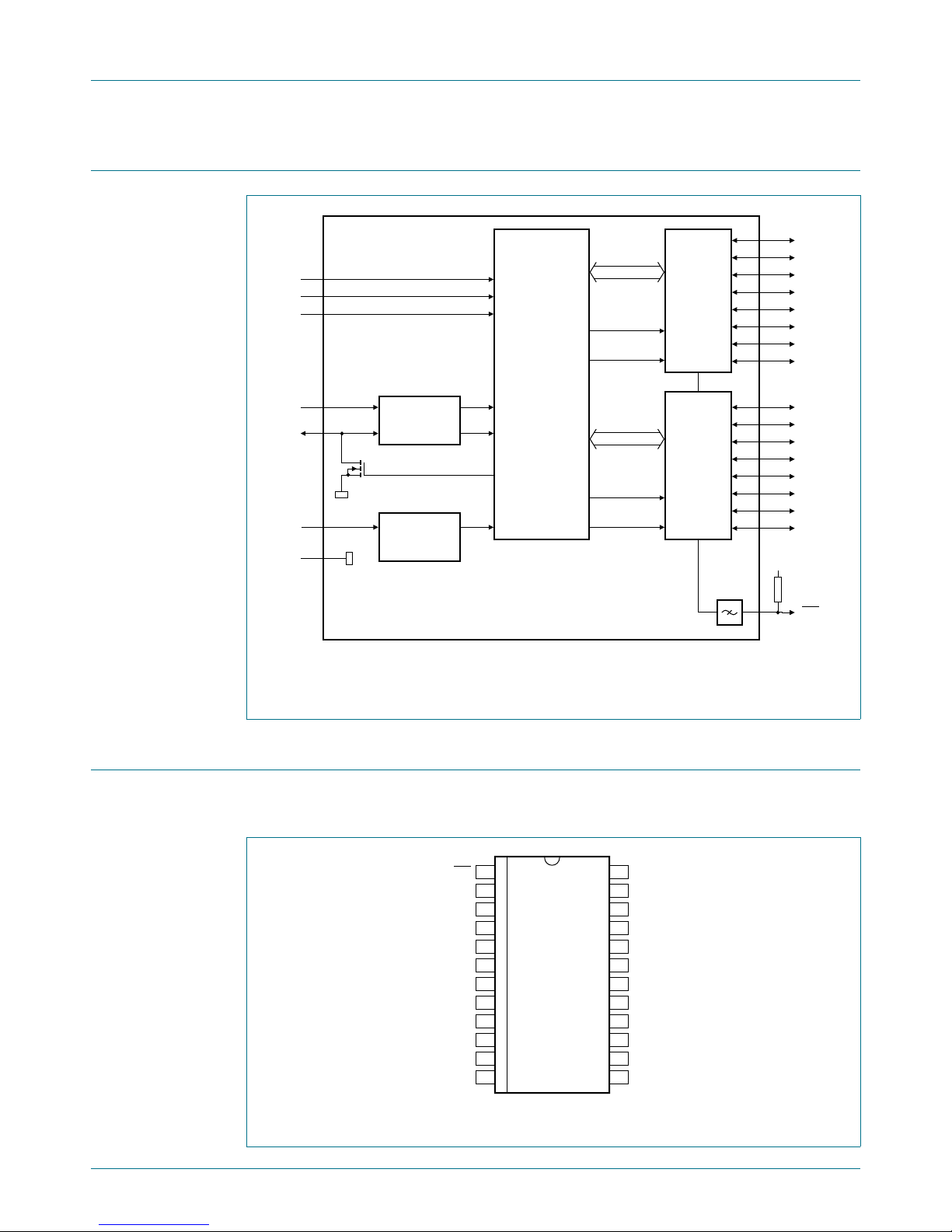
4. Block diagram
PCA9555
16-bit I2C-bus and SMBus I/O port with interrupt
Fig 1. Block diagram of PCA9555
5. Pinning information
PCA9555 All information provided in this document is subject to legal disclaimers. © NXP Semiconductors N.V. 2017. All rights reserved.
Product data sheet Rev. 10 — 8 November 2017 3 of 34
5.1 Pinning
Fig 2. Pin configuration for SO24
Remark: All I/Os are set to inputs at reset.
NXP Semiconductors
INT
A1
A2
IO0_0
IO0_1
IO0_2
IO0_3
IO0_4
IO0_5
IO0_6
IO0_7
V
SS
PCA9555DB
002aac699
1
2
3
4
5
6
7
8
9
10
11
12
14
13
16
15
18
17
20
19
22
21
24
23
V
DD
SDA
SCL
A0
IO1_7
IO1_6
IO1_5
IO1_4
IO1_3
IO1_2
IO1_1
IO1_0
V
DD
SDA
SCL
A0
IO1_7
IO1_6
IO1_5
IO1_4
IO1_3
IO1_2
IO1_1
IO1_0
INT
A1
A2
IO0_0
IO0_1
IO0_2
IO0_3
IO0_4
IO0_5
IO0_6
IO0_7
V
SS
PCA9555PW
002aac700
1
2
3
4
5
6
7
8
9
10
11
12
14
13
16
15
18
17
20
19
22
21
24
23
002aac701
PCA9555BS
Transparent top view
IO1_3
IO0_4
IO0_5
IO1_4
IO0_3 IO1_5
IO0_2 IO1_6
IO0_1 IO1_7
IO0_0 A0
IO0_6
IO0_7
V
SS
IO1_0
IO1_1
IO1_2
A2
A1
V
DD
SDA
SCL
terminal 1
index area
6
13
5
14
4 15
3 16
2 17
1
18
7
8
9
101112
2423222120
19
INT
002aac881
Transparent top view
IO1_3
IO0_4
IO0_5
IO1_4
IO0_3 IO1_5
IO0_2 IO1_6
IO0_1 IO1_7
IO0_0 A0
IO0_6
IO0_7
V
SS
IO1_0
IO1_1
IO1_2
A2A1INT
V
DD
SDA
SCL
terminal 1
index area
6
13
5
14
4 15
3 16
2 17
1
18
7
8
9
101112
2423222120
19
PCA9555HF
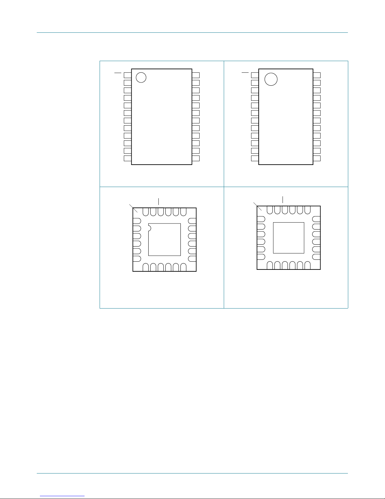
Fig 3. Pin configuration for SSOP24 Fig 4. Pin configuration for TSSOP24
PCA9555
16-bit I2C-bus and SMBus I/O port with interrupt
Fig 5. Pin configuration for HVQFN24 Fig 6. Pin configuration for HWQFN24
PCA9555 All information provided in this document is subject to legal disclaimers. © NXP Semiconductors N.V. 2017. All rights reserved.
Product data sheet Rev. 10 — 8 November 2017 4 of 34
NXP Semiconductors
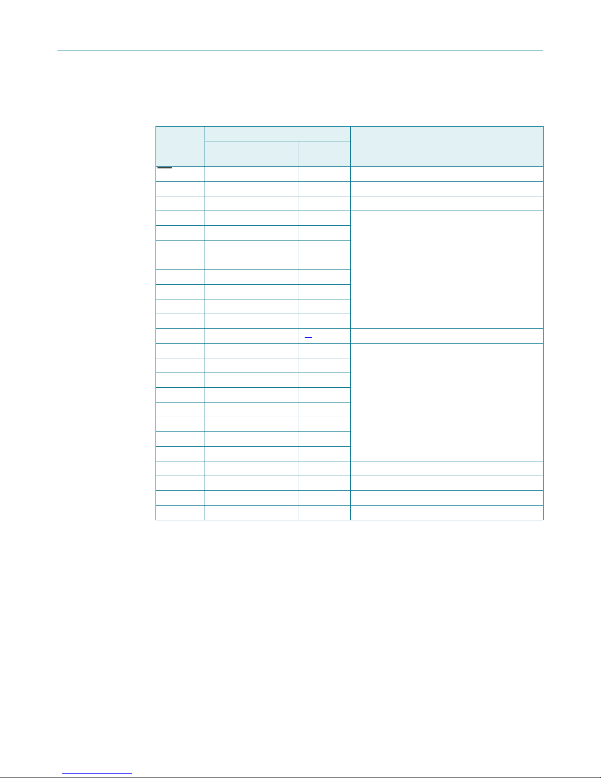
5.2 Pin description
Table 3. Pin description
Symbol Pin Description
INT
A1 2 23 address input 1
A2 3 24 address input 2
IO0_0 4 1 port 0 input/output
IO0_1 5 2
IO0_2 6 3
IO0_3 7 4
IO0_4 8 5
IO0_5 9 6
IO0_6 10 7
IO0_7 11 8
V
SS
IO1_0 13 10 port 1 input/output
IO1_1 14 11
IO1_2 15 12
IO1_3 16 13
IO1_4 17 14
IO1_5 18 15
IO1_6 19 16
IO1_7 20 17
A0 21 18 address input 0
SCL 22 19 serial clock line
SDA 23 20 serial data line
V
DD
[1] HVQFN and HWQFN package die supply ground is connected to both the VSS pin and the exposed center
PCA9555
16-bit I2C-bus and SMBus I/O port with interrupt
SO24, SSOP24,
TSSOP24
1 22 interrupt output (open-drain)
12 9
24 21 supply voltage
pad. The V
electrical, and board-level performance, the exposed pad needs to be soldered to the board using a
corresponding thermal pad on the board, and for proper heat conduction through the board thermal vias
need to be incorporated in the PCB in the thermal pad region.
pin must be connected to supply ground for proper device operation. For enhanced thermal,
SS
HVQFN24,
HWQFN24
[1]
supply ground
PCA9555 All information provided in this document is subject to legal disclaimers. © NXP Semiconductors N.V. 2017. All rights reserved.
Product data sheet Rev. 10 — 8 November 2017 5 of 34
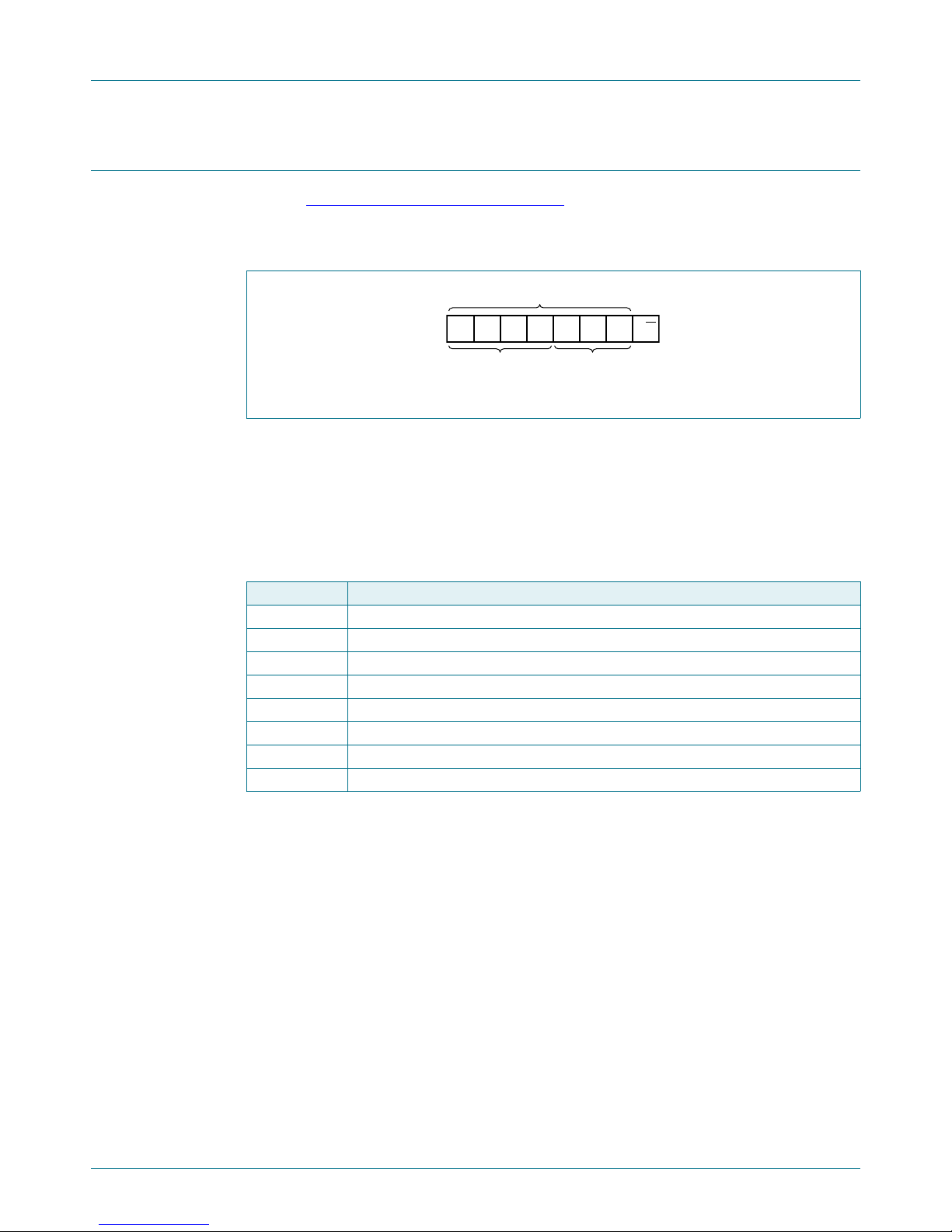
NXP Semiconductors
R/W
002aac219
0 1 0 0 A2 A1 A0
programmable
slave address
fixed
6. Functional description
Refer to Figure 1 “Block diagram of PCA9555”.
6.1 Device address
Fig 7. PCA9555 device address
6.2 Registers
6.2.1 Command byte
PCA9555
16-bit I2C-bus and SMBus I/O port with interrupt
The command byte is the first byte to follow the address byte during a write transmission.
It is used as a pointer to determine which of the following registers will be written or read.
Table 4. Command byte
Command Register
0 Input port 0
1 Input port 1
2 Output port 0
3 Output port 1
4 Polarity Inversion port 0
5 Polarity Inversion port 1
6 Configuration port 0
7 Configuration port 1
PCA9555 All information provided in this document is subject to legal disclaimers. © NXP Semiconductors N.V. 2017. All rights reserved.
Product data sheet Rev. 10 — 8 November 2017 6 of 34
NXP Semiconductors
6.2.2 Registers 0 and 1: Input port registers
This register is an input-only port. It reflects the incoming logic levels of the pins,
regardless of whether the pin is defined as an input or an output by Register 3. Writes to
this register have no effect.
The default value ‘X’ is determined by the externally applied logic level.
Table 5. Input port 0 Register
Bit 7 6 5 4 3 2 1 0
Symbol I0.7 I0.6 I0.5 I0.4 I0.3 I0.2 I0.1 I0.0
Default XXXXXXXX
Table 6. Input port 1 register
Bit 7 6 5 4 3 2 1 0
Symbol I1.7 I1.6 I1.5 I1.4 I1.3 I1.2 I1.1 I1.0
Default XXXXXXXX
6.2.3 Registers 2 and 3: Output port registers
PCA9555
16-bit I2C-bus and SMBus I/O port with interrupt
This register is an output-only port. It reflects the outgoing logic levels of the pins defined
as outputs by Registers 6 and 7. Bit values in this register have no effect on pins defined
as inputs. In turn, reads from this register reflect the value that is in the flip-flop controlling
the output selection, not the actual pin value.
T able 7. Output port 0 register
Bit 7 6 5 4 3 2 1 0
Symbol O0.7 O0.6 O0.5 O0.4 O0.3 O0.2 O0.1 O0.0
Default 11111111
T able 8. Output port 1 register
Bit 7 6 5 4 3 2 1 0
Symbol O1.7 O1.6 O1.5 O1.4 O1.3 O1.2 O1.1 O1.0
Default 11111111
6.2.4 Registers 4 and 5: Polarity Inversion registers
This register allows the user to invert the polarity of the Input port register data. If a bit in
this register is set (written with ‘1’), the Input port data polarity is inverted. If a bit in this
register is cleared (written with a ‘0’), the Input port data polarity is retained.
Table 9. Polarity Inversion port 0 register
Bit 7 6 5 4 3 2 1 0
Symbol N0.7 N0.6 N0.5 N0.4 N0.3 N0.2 N0.1 N0.0
Default 00000000
Table 10. Polarity Inversion port 1 register
Bit 7 6 5 4 3 2 1 0
Symbol N1.7 N1.6 N1.5 N1.4 N1.3 N1.2 N1.1 N1.0
Default 00000000
PCA9555 All information provided in this document is subject to legal disclaimers. © NXP Semiconductors N.V. 2017. All rights reserved.
Product data sheet Rev. 10 — 8 November 2017 7 of 34
NXP Semiconductors
6.2.5 Registers 6 and 7: Configuration registers
This register configures the directions of the I/O pins. If a bit in this register is set (written
with ‘1’), the corresponding port pin is enabled as an input with high-impedance output
driver. If a bit in this register is cleared (written with ‘0’), the corresponding port pin is
enabled as an output. Note that there is a high value resistor tied to V
reset, the device's ports are inputs with a pull-up to V
T able 11. Configuration port 0 register
Bit 7 6 5 4 3 2 1 0
Symbol C0.7 C0.6 C0.5 C0.4 C0.3 C0.2 C0.1 C0.0
Default 11111111
T able 12. Configuration port 1 register
Bit 7 6 5 4 3 2 1 0
Symbol C1.7 C1.6 C1.5 C1.4 C1.3 C1.2 C1.1 C1.0
Default 11111111
PCA9555
16-bit I2C-bus and SMBus I/O port with interrupt
at each pin. At
DD
.
DD
6.3 Power-on reset
When power is applied to VDD, an internal power-on reset holds the PCA9555 in a reset
condition until V
has reached V
DD
. At that point, the reset condition is released and the
POR
PCA9555 registers and SMBus state machine will initialize to their default states. The
power-on reset typically completes the reset and enables the part by the time the power
supply is above V
. However, when it is required to reset the part by lowering the power
POR
supply, it is necessary to lower it below 0.2 V.
6.4 I/O port
When an I/O is configured as an input, FETs Q1 and Q2 are off, creating a
high-impedance input with a weak pull-up to V
V
to a maximum of 5.5 V.
DD
If the I/O is configured as an output, then either Q1 or Q2 is on, depending on the state of
the Output Port register. Care should be exercised if an external voltage is applied to an
I/O configured as an output because of the low-impedance path that exists between the
pin and either V
or VSS.
DD
. The input voltage may be raised above
DD
PCA9555 All information provided in this document is subject to legal disclaimers. © NXP Semiconductors N.V. 2017. All rights reserved.
Product data sheet Rev. 10 — 8 November 2017 8 of 34
NXP Semiconductors
V
DD
I/O pin
output port
register data
configuration
register
DQ
CK Q
data from
shift register
write
configuration
pulse
output port
register
DQ
CK
write pulse
polarity inversion
register
DQ
CK
data from
shift register
write polarity
pulse
input port
register
DQ
CK
read pulse
input port
register data
polarity
inversion
register data
002aac703
FF
data from
shift register
FF
FF
FF
Q1
Q2
V
SS
to INT
100 kΩ
PCA9555
16-bit I2C-bus and SMBus I/O port with interrupt
Fig 8. Simplified schematic of I/Os
6.5 Bus transactions
6.5.1 Writing to the port registers
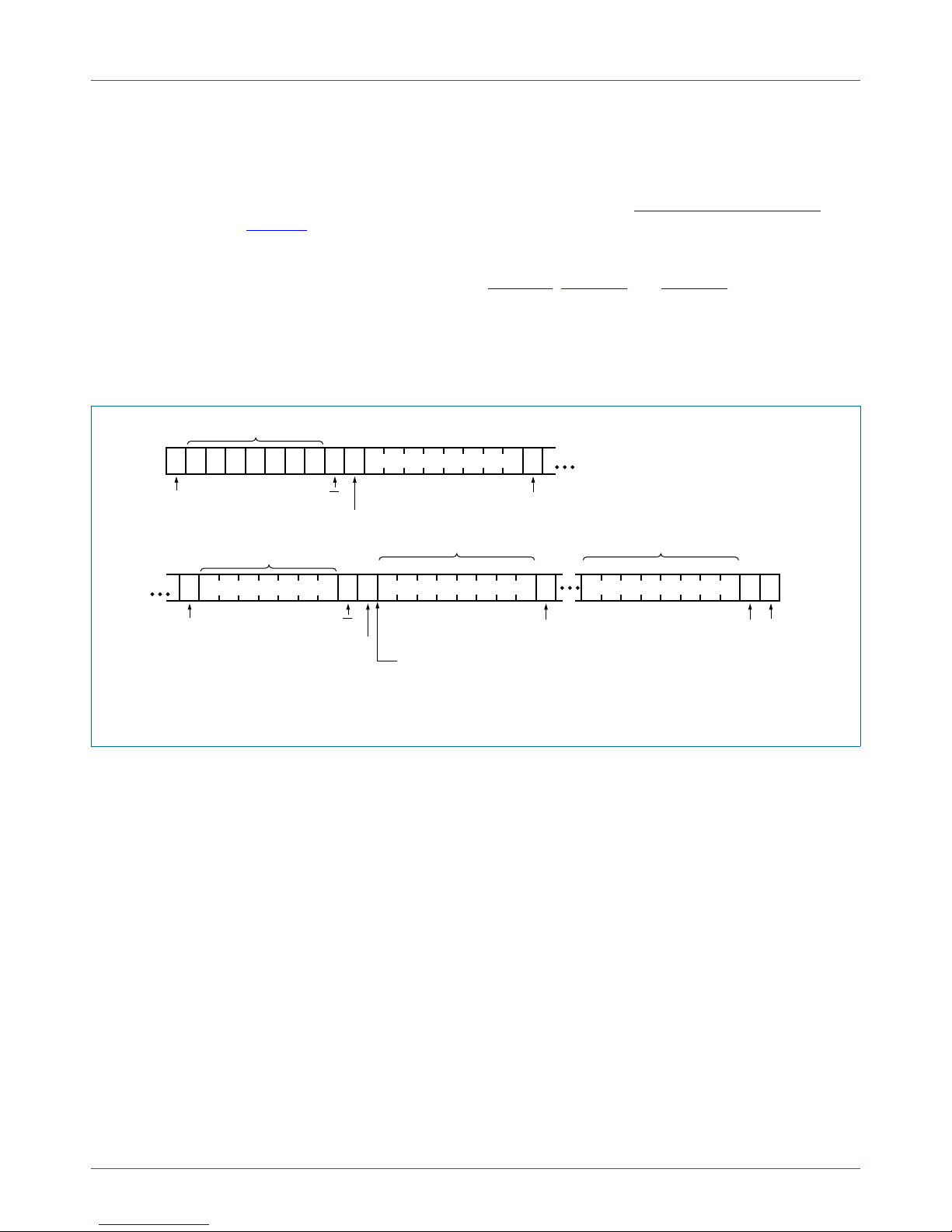
Data is transmitted to the PCA9555 by sending the device address and setting the least
significant bit to a logic 0 (see Figure 7 “
sent after the address and determines which register will receive the data following the
command byte.
PCA9555 All information provided in this document is subject to legal disclaimers. © NXP Semiconductors N.V. 2017. All rights reserved.
Product data sheet Rev. 10 — 8 November 2017 9 of 34
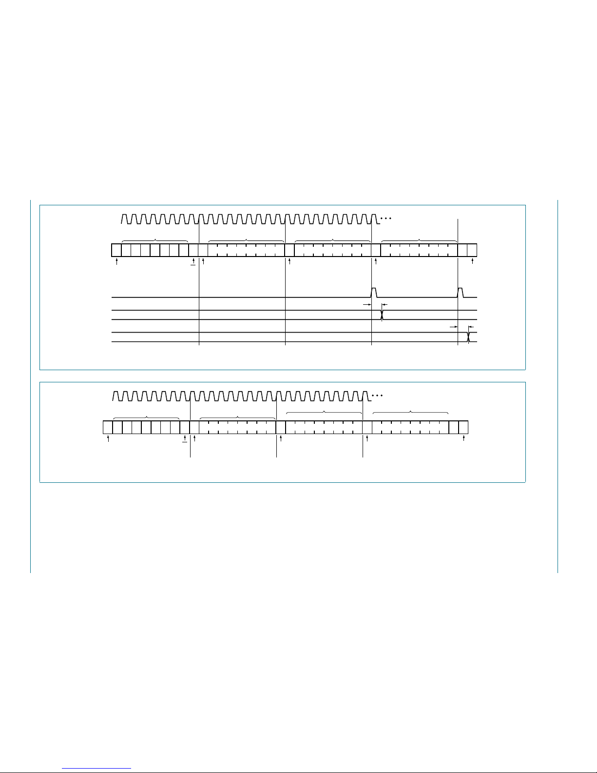
The eight registers within the PCA9555 are configured to operate as four register pairs.
The four pairs are Input Ports, Output Ports, Polarity Inversion Ports, and Configuration
Ports. After sending data to one register, the next data byte will be sent to the other
register in the pair (see Figure 9
Output Port 1 (register 3), then the next byte will be stored in Output Port 0 (register 2).
There is no limitation on the number of data bytes sent in one write transmission. In this
way, each 8-bit register may be updated independently of the other registers.
At power-on reset, all registers return to default values.
PCA9555 device address”). The command byte is
and Figure 10). For example, if the first byte is sent to
xxxxxxxxxxxxxxxxxxxxx xxxxxxxxxxxxxxxxxxxxxxxxxx xxxxxxx x x x xxxxxxxxxxxxxxxxxxxxxxxxxxxxxx xxxxxxxxxxxxxxxxxxx xx xx xxxxx
xxxxxxxxxxxxxxxxxxxxxxxxxxx xxxxxxxxxxxxxxxxxxx xxxxxx xxxxxxxxxxxxxxxxxxxxxxxxxxxxxxxxxxx xxxxxxxxxxxx x x
xxxxxxxxxxxxxxxxxxxxx xxxxxxxxxxxxxxxxxxxxxxxxxxxxxx xxxxx xxxxxxxxxxxxxxxxxxxxxxxxxxxxxxxxxxxxxxxxxxxxxxxxxx xxxxxxxx
xxxxxxxxxxxxxxxxxxxxxxxxx xxxxxxxxxxxxxxxxxxxx xxx
PCA9555 All information provided in this document is subject to legal disclaimers. © NXP Semiconductors N.V. 2017. All rights reserved.
Product data sheet Rev. 10 — 8 November 2017 10 of 34
NXP Semiconductors
PCA9555
16-bit I
2
C-bus and SMBus I/O port with interrupt
Fig 9. Write to Output port registers
1 0 0 A2 A1 A0 0 AS0
START condition R/W acknowledge
from slave
002aac220
A
SCL
SDA A
write to port
data out
from port 0
P
t
v(Q)
987654321
command byte
data to port 0
DATA 0
slave address
00000100
STOP
condition
0.00.7
acknowledge
from slave
acknowledge
from slave
data to port 1
DATA 1 1.01.7
A
data out
from port 1
t
v(Q)
DATA VALID
Fig 10. Write to Configuration registers
1 0 0 A2 A1 A0 0 AS0
START condition R/W acknowledge
from slave
002aac221
A
SCL
SDA A P
987654321
command byte
data to register
DATA 0
slave address
00001100
STOP
condition
LSBMSB
acknowledge
from slave
acknowledge
from slave
data to register
DATA 1
LSBMSB
A
NXP Semiconductors
AS
START condition R/W
acknowledge
from slave
002aac222
A
acknowledge
from slave
SDA
A P
acknowledge
from master
DATA (first byte)
slave address
STOP
condition
S
(repeated)
START condition
(cont.)
(cont.)
1 0 0 A2 A1 A0 1 A0
R/W
acknowledge
from slave
slave address
at this moment master-transmitter becomes master-receiver
and slave-receiver becomes slave-transmitter
NA
no acknowledge
from master
COMMAND BYTE
1 0 0 A2 A1 A00 0
data from lower or
upper byte of register
LSBMSB
DATA (last byte)
data from upper or
lower byte of register
LSBMSB
6.5.2 Reading the port registers
In order to read data from the PCA9555, the bus master must first send the PCA9555
address with the least significant bit set to a logic 0 (see Figure 7 “
address”). The command byte is sent after the address and determines which register will
be accessed. After a restart, the device address is sent again, but this time the least
significant bit is set to a logic 1. Data from the register defined by the command byte will
then be sent by the PCA9555 (see Figure 11
into the register on the falling edge of the acknowledge clock pulse. After the first byte is
read, additional bytes may be read but the data will now reflect the information in the other
register in the pair . For examp le, if you read Input Port 1, then the next byte read would be
Input Port 0. There is no limitation on the number of data bytes received in one read
transmission but the final byte received, the bus master must not acknowledge the data.
PCA9555
16-bit I2C-bus and SMBus I/O port with interrupt
PCA9555 device
, Figure 12 and Figure 13). Data is clocked
Fig 11. Read from register
Remark: Transfer can be stopped at any time by a STOP condition.
PCA9555 All information provided in this document is subject to legal disclaimers. © NXP Semiconductors N.V. 2017. All rights reserved.
Product data sheet Rev. 10 — 8 November 2017 11 of 34
 Loading...