

Page 1

UM10147
P89LPC952/954 User manual
Rev. 02 — 28 April 2008 User manual
Document information
Info Content
Keywords P89LPC952, P89LPC954
Abstract Technical information for the P89LPC952/954 devices.
Page 2

NXP Semiconductors
UM10147
P89LPC952/954 User manual
Revision history
Rev Date Description
02 20080428 Added LQFP48 package information
01 20070917 Initial version
Contact information
For more information, please visit: http://www.nxp.com
For sales office addresses, please send an email to: salesaddresses@nxp.com
UM10147_2 © NXP B.V. 2008. All rights reserved.
User manual Rev. 02 — 28 April 2008 2 of 134
Page 3
NXP Semiconductors
1. Introduction
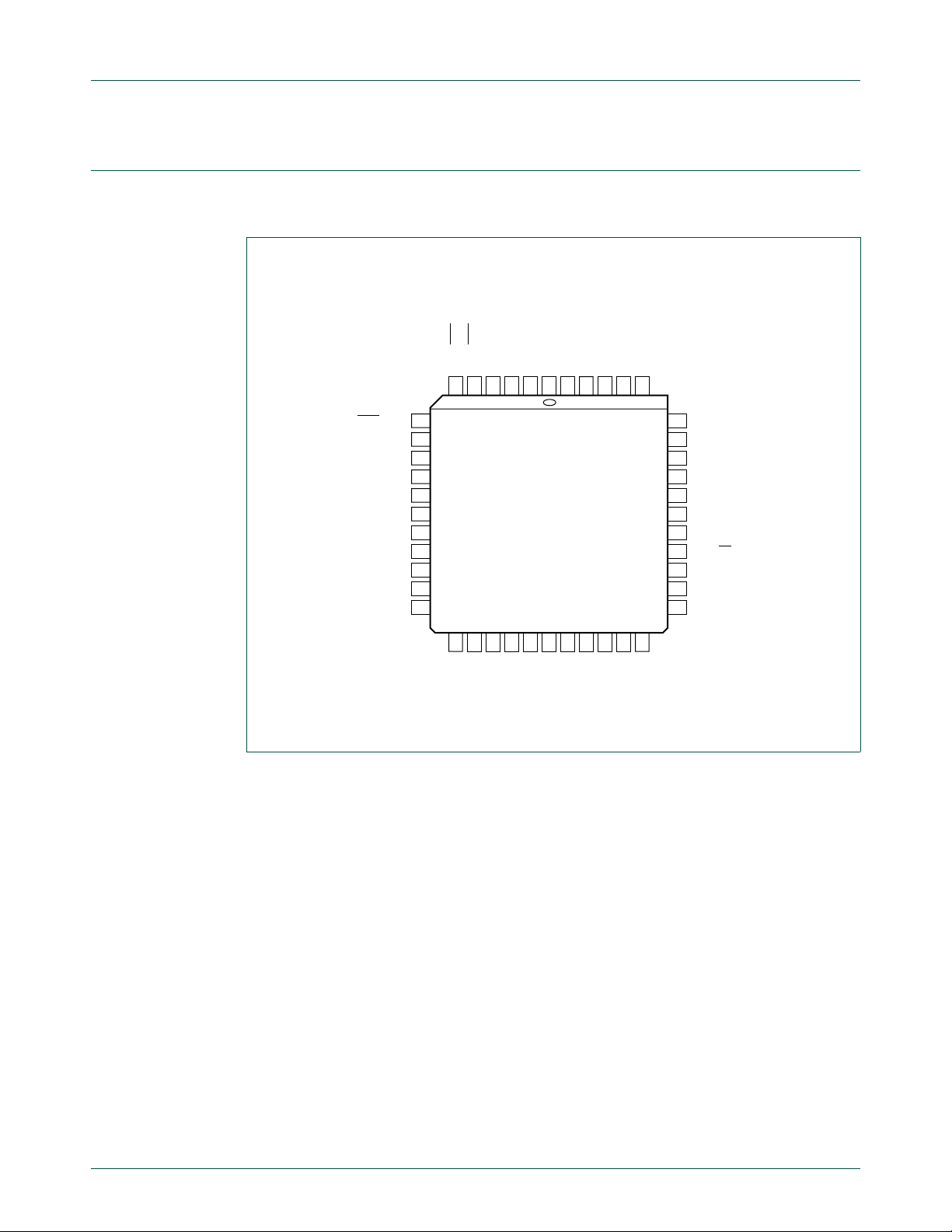
1.1 Pin configuration
UM10147
P89LPC952/954 User manual
P1.4/INT1
6
V
DD
P5.7
P5.6
P5.5
P5.4
7
8
9
10
11
12
13
14
15
16
17
181920212223242526
P5.3
P1.3/INT0/SDA
P1.2/T0/SCL
P1.1/RXD0
P1.0/TXD0
P3.1/XTAL1
P3.0/XTAL2/CLKOUT
Fig 1. PLCC44 pin configuration
SS
P1.5/RST
P1.6
V
5
4
3
P89LPC952FA
P89LPC954FA
P5.2
P5.1
P5.0
P1.7/AD04
P2.0/AD07
2
1
44
SS
V
P4.6 P2.1/AD06
P4.7/TCLK
43
424140
39
38
37
36
35
34
33
32
31
30
29
27
28
002aab307
P4.4 P0.1/CIN2B/KBI1/AD00
P4.5/TDI P0.0/CMP2/KBI0/AD05
P4.2/TXD1 P0.3/CIN1B/KBI3/AD02
P4.3/RXD1 P0.2/CIN2A/KBI2/AD01
P0.4/CIN1A/KBI4/AD03
P0.5/CMPREF/KBI5
P0.6/CMP1/KBI6
V
DD
P0.7/T1/KBI7
P2.2/MOSI
P2.3/MISO
P2.4/SS
P2.5/SPICLK
P4.0
P4.1/TRIG
UM10147_2 © NXP B.V. 2008. All rights reserved.
User manual Rev. 02 — 28 April 2008 3 of 134
Page 4
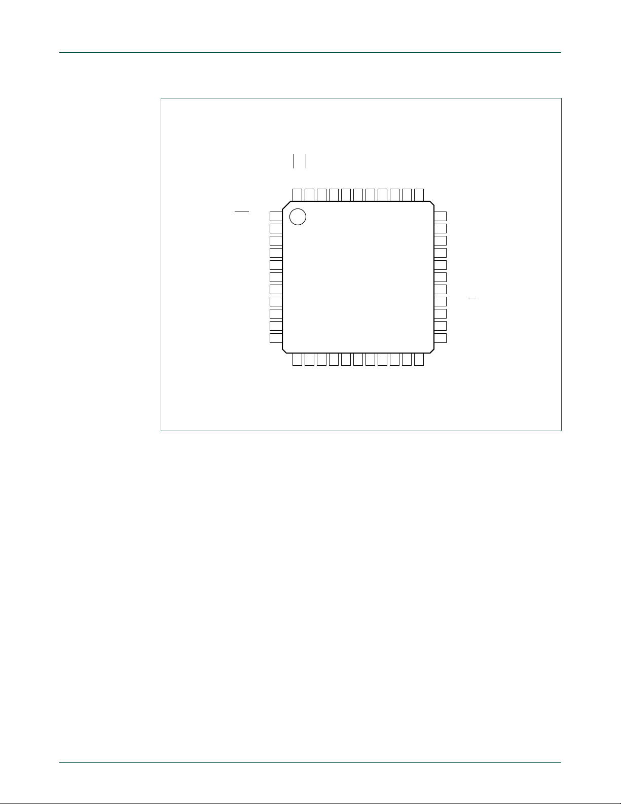
NXP Semiconductors
P1.4/INT1
P1.5/RST
P1.6
VSSP1.7/AD04
P2.0/AD07
P2.1/AD06
P0.0/CMP2/KBI0/AD05
P0.1/CIN2B/KBI1/AD00
P0.2/CIN2A/KBI2/AD01
4443424140393837363534
UM10147
P89LPC952/954 User manual
P0.3/CIN1B/KBI3/AD02
V
DD
P5.7
P5.6
P5.5
P5.4
1
2
3
4
5
6
7
8
9
10
11
1213141516171819202122
P5.3
P1.3/INT0/SDA
P1.2/T0/SCL
P1.1/RXD0
P1.0/TXD0
P3.1/XTAL1
P3.0/XTAL2/CLKOUT
Fig 2. LQFP44 pin configuration
P89LPC952FBD
P89LPC954FBD
P5.1
P5.0
V
P5.2
SS
P4.7/TCLK
P4.6
P4.4
P4.5/TDI
33
32
31
30
29
28
27
26
25
24
23
002aab306
P4.2/TXD1
P4.3/RXD1
P0.4/CIN1A/KBI4/AD03
P0.5/CMPREF/KBI5
P0.6/CMP1/KBI6
V
DD
P0.7/T1/KBI7
P2.2/MOSI
P2.3/MISO
P2.4/SS
P2.5/SPICLK
P4.0
P4.1/TRIG
UM10147_2 © NXP B.V. 2008. All rights reserved.
User manual Rev. 02 — 28 April 2008 4 of 134
Page 5
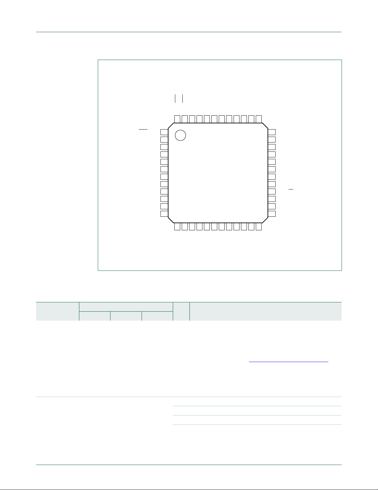
NXP Semiconductors
UM10147
P89LPC952/954 User manual
VREFN
P1.6
VSSP1.7/AD04
P2.0/AD07
P89LPC954FBD48
SS
V
P5.1
P5.0
P4.6
P4.7/TCLK
P2.1/AD06
P0.0/CMP2/KBI0/AD05
P0.1/CIN2B/KBI1/AD00
P0.2/CIN2A/KBI2/AD01
P0.3/CIN1B/KBI3/AD02
37
24
P4.4
P4.5/TDI
P4.1/TRIG
P4.2/TXD1
P4.3/RXD1
36
P0.4/CIN1A/KBI4/AD03
35
P0.5/CMPREF/KBI5
34
P0.6/CMP1/KBI6
33
VREFP
32
V
DD
31
P0.7/T1/KBI7
30
P2.2/MOSI
29
P2.3/MISO
28
P2.4/SS
27
P2.5/SPICLK
26
P2.6
25
P4.0
002aad095
P1.3/INT0/SDA
P1.2/T0/SCL
P1.1/RXD0
P1.0/TXD0
P2.7
P3.1/XTAL1
P3.0/XTAL2/CLKOUT
V
DD
P5.7
P5.6
P5.5
P5.4
P1.4/INT1
P1.5/RST
4847464544434241403938
1
2
3
4
5
6
7
8
9
10
11
12
1314151617181920212223
P5.3
P5.2
Fig 3. LQFP48 pin configuration
1.2 Pin description
Table 1. Pin description
Symbol Pin Type Description
P0.0 to P0.7 I/O Port 0: Port 0 is an 8-bit I/O port with a user-configurable
P0.0/CMP2/
KBI0/AD05
LQFP48 PLCC44 LQFP44
output type. During reset Port 0 latches are configured in the
input only mode with the internal pull-up disabled. The
operation of Port 0 pins as inputs and outputs depends upon
the port configuration selected. Each port pin is configured
independently. Refer to Section 5.1 “
The Keypad Interrupt feature operates with Port 0 pins.
All pins have Schmitt triggered inputs.
Port 0 also provides various special functions as described
below:
40 43 37 I/O P0.0 — Port 0 bit 0.
O CMP2 — Comparator 2 output.
I KBI0 — Keyboard input 0.
I AD05 — ADC0 channel 5 analog input.
Port configurations” .
UM10147_2 © NXP B.V. 2008. All rights reserved.
User manual Rev. 02 — 28 April 2008 5 of 134
Page 6

NXP Semiconductors
UM10147
P89LPC952/954 User manual
Table 1. Pin description
Symbol Pin Type Description
LQFP48 PLCC44 LQFP44
P0.1/CIN2B/
KBI1/AD00
P0.2/CIN2A/
KBI2/AD01
P0.3/CIN1B/
KBI3/AD02
P0.4/CIN1A/
KBI4/AD03
P0.5/CMPREF/
KBI5
P0.6/CMP1/
KBI6
P0.7/T1/KBI7313529I/OP0.7 — Port 0 bit 7.
P1.0 to P1.7 I/O, I
P1.0/TXD0 4 10 4 I/O P1.0 — Port 1 bit 0.
P1.1/RXD0393I/OP1.1 — Port 1 bit 1.
39 42 36 I/O P0.1 — Port 0 bit 1.
38 41 35 I/O P0.2 — Port 0 bit 2.
37 40 34 I/O P0.3 — Port 0 bit 3.
36 39 33 I/O P0.4 — Port 0 bit 4.
35 38 32 I/O P0.5 — Port 0 bit 5.
34 37 31 I/O P0.6 — Port 0 bit 6.
…continued
I CIN2B — Comparator 2 positive input B.
I KBI1 — Keyboard input 1.
I AD00 — ADC0 channel 0 analog input.
I CIN2A — Comparator 2 positive input A.
I KBI2 — Keyboard input 2.
I AD01 — ADC0 channel 1 analog input.
I CIN1B — Comparator 1 positive input B.
I KBI3 — Keyboard input 3.
I AD02 — ADC0 channel 2 analog input.
I CIN1A — Comparator 1 positive input A.
I KBI4 — Keyboard input 4.
I AD03 — ADC0 channel 3 analog input.
I CMPREF — Comparator reference (negative) input.
I KBI5 — Keyboard input 5.
O CMP1 — Comparator 1 output.
I KBI6 — Keyboard input 6.
I/O T1 — Timer/counter 1 external count input or overflow
output.
I KBI7 — Keyboard input 7.
Port 1: Port 1 is an 8-bit I/O port with a user-configurable
[1]
output type, except for three pins as noted below. During
reset Port 1 latches are configured in the input only mode
with the internal pull-up disabled. The operation of the
configurable Port 1 pins as inputs and outputs depends upon
the port configuration selected. Each of the configurable port
pins are programmed independently. Refer to Section 5.1
“Port configurations”. P1.2 to P1.3 are open drain when used
as outputs. P1.5 is input only.
All pins have Schmitt triggered inputs.
Port 1 also provides various special functions as described
below:
O TXD0 — Transmitter output for serial port 0.
I RXD0 — Receiver input for serial port 0.
UM10147_2 © NXP B.V. 2008. All rights reserved.
User manual Rev. 02 — 28 April 2008 6 of 134
Page 7

NXP Semiconductors
UM10147
P89LPC952/954 User manual
Table 1. Pin description
…continued
Symbol Pin Type Description
LQFP48 PLCC44 LQFP44
P1.2/T0/SCL282I/OP1.2 — Port 1 bit 2 (open-drain when used as output).
I/O T0 — Timer/counter 0 external count input or overflow output
(open-drain when used as output).
2
C-bus serial clock input/output.
— External interrupt 0 input.
2
C-bus serial data input/output.
— External interrupt 1 input.
— External Reset input during power-on or maybe a
P1.3/INT0
P1.4/INT1
P1.5/RST
I/O SCL — I
/SDA171I/OP1.3 — Port 1 bit 3 (open-drain when used as output).
I INT0
I/O SDA — I
48 6 44 I/O P1.4 — Port 1 bit 4.
I INT1
47 5 43 I P1.5 — Port 1 bit 5 (input only).
I RST
reset input/output if selected via UCFG1 and UCFG2. When
functioning as a reset input or input/output, a LOW on this
pin resets the microcontroller, causing I/O ports and
peripherals to take on their default states, and the processor
begins execution at address 0. When functioning as a reset
output or input/output an internal reset source will drive this
pin LOW. Also used during a power-on sequence to force
ISP mode. When using an oscillator frequency above
12 MHz, the reset input function of P1.5 must be
enabled. An external circuit is required to hold the
device in reset at power-up until V
has reached its
DD
specified level. When system power is removed VDD will
fall below the minimum specified operating voltage.
When using an oscillator frequency above 12 MHz, in
some applications, an external brownout detect circuit
may be required to hold the device in reset when V
DD
falls below the minimum specified operating voltage.
P1.6 46 4 42 I/O P1.6 — Port 1 bit 6.
P1.7/AD04 43 2 40 I/O P1.7 — Port 1 bit 7.
I AD04 — ADC0 channel 4 analog input.
P2.0 to P2.5 I/O Port 2: Port 2 is an 8-bit I/O port with a user-configurable
output type. During reset Port 2 latches are configured in the
input only mode with the internal pull-up disabled. The
operation of Port 2 pins as inputs and outputs depends upon
the port configuration selected. Each port pin is configured
independently. Refer to Section 5.1 “
Port configurations”.
All pins have Schmitt triggered inputs.
Port 2 also provides various special functions as described
below:
P2.0/AD07 42 1 39 I/O P2.0 — Port 2 bit 0.
I AD07 — ADC0 channel 7 analog input.
P2.1/AD06414438I/OP2.1 — Port 2 bit 1.
I AD06 — ADC0 channel 6 analog input.
UM10147_2 © NXP B.V. 2008. All rights reserved.
User manual Rev. 02 — 28 April 2008 7 of 134
Page 8

NXP Semiconductors
UM10147
P89LPC952/954 User manual
Table 1. Pin description
Symbol Pin Type Description
LQFP48 PLCC44 LQFP44
P2.2/MOSI303428I/OP2.2 — Port 2 bit 2.
P2.3/MISO293327I/OP2.3 — Port 2 bit 3.
P2.4/SS
P2.5/SPICLK273125I/OP2.5 — Port 2 bit 5.
P2.6 26 - - I/O P2.6 — Port 2 bit 6.
P2.7 5 - - I/O P2.7 — Port 2 bit 7.
P3.0 to P3.1 I/O Port 3: Port 3 is a 2-bit I/O port with a user-co n fi g urable
P3.0/XTAL2/
CLKOUT
P3.1/XTAL1 6 1 1 5 I/O P3.1 — Port 3 bit 1.
P4.0 to P4.7 I/O Port 4: Port 4 is an 8-bit I/O port with a user-configurable
28 32 26 I/O P2.4 — Port 2 bit 4.
7126I/OP3.0 — Port 3 bit 0.
…continued
I/O MOSI — SPI master out slave in. When configured as
master, this pin is output; when configured as slave, this pin
is input.
I/O MISO — When configured as master, this pin is input, when
configured as slave, this pin is output.
I/O SS
I/O SPICLK — SPI clock. When configured as master, this pin is
O XTAL2 — Output from the oscillator amplifier (when a crystal
O CLKOUT — CPU clock divided by 2 when enabled via SFR
I XTAL1 — Input to the oscillator circuit and internal clock
— SPI Slave select.
output; when configured as slave, this pin is input.
output type. During reset Port 3 latches are configured in the
input only mode with the internal pull-up disabled. The
operation of Port 3 pins as inputs and outputs depends upon
the port configuration selected. Each port pin is configured
independently. Refer to Section 5.1 “
All pins have Schmitt triggered inputs.
Port 3 also provides various special functions as described
below:
oscillator option is selected via the flash configuration.
bit (ENCLK -TRIM.6). It can be used if the CPU clock is the
internal RC oscillator, watchdog oscillator or external clock
input, except when XTAL1/XT AL2 are used to generate clock
source for the RTC/system timer.
generator circuits (when selected via the flash configuration).
It can be a port pin if internal RC oscillator or watchdog
oscillator is used as the CPU clock source, and if
XTAL1/XTAL 2 a re no t used to generate the clock for the
RTC/system timer.
output type. During reset Port 4 latches are configured in the
input only mode with the internal pull-up disabled. The
operation of Port 4 pins as inputs and outputs depends upon
the port configuration selected. Each port pin is configured
independently. Refer to Section 5.1 “
All pins have Schmitt triggered inputs.
Port 4 also provides various special functions as described
below:
Port configurations”.
Port configurations”.
UM10147_2 © NXP B.V. 2008. All rights reserved.
User manual Rev. 02 — 28 April 2008 8 of 134
Page 9

NXP Semiconductors
UM10147
P89LPC952/954 User manual
Table 1. Pin description
…continued
Symbol Pin Type Description
LQFP48 PLCC44 LQFP44
P4.0 25 30 24 I/O P4.0 — Port 4 bit 0.
P4.1/TRIG242923I/OP4.1 — Port 4 bit 1.
O TRIG — Debugger trigger output.
P4.2/TXD1232822I/OP4.2 — Port 4 bit 2.
O TXD1 — Transmitter output for serial port 1.
P4.3/RXD1222721I/OP4.3 — Port 4 bit 3.
I RXD1 — Receiver input for serial port 1.
P4.4 21 26 20 I/O P4.4 — Port 4 bit 4.
P4.5/TDI 20 25 19 I/O P4.5 — Port 4 bit 5.
I/O TDI — Serial data input/output for debugger interface.
P4.6 19 24 18 I/O P4.6 — Port 4 bit 6.
P4.7/TCLK182317I/OP4.7 — Port 4 bit 7.
I TCLK — Serial clock input for debugger interface.
P5.0 to P5.7 I/O Port 5: Port 5 is an 8-bit I/O port with a user-configurable
output type. During reset Port 5 latches are configured in the
input only mode with the internal pull-up disabled. The
operation of Port 5 pins as inputs and outputs depends upon
the port configuration selected. Each port pin is configured
independently. Refer to Section 5.1 “
Port configurations”.
All pins have Schmitt triggered inputs.
Port 5 also provides various special functions as described
below:
P5.0 16 21 15 I/O P5.0 — Port 5 bit 0. High current output.
P5.1 15 20 14 I/O P5.1 — Port 5 bit 1. High current output.
P5.2 14 19 13 I/O P5.2 — Port 5 bit 2. High current output.
P5.3 13 18 12 I/O P5.3 — Port 5 bit 3. High current output.
P5.4 12 17 1 1 I/O P5.4 — Port 5 bit 4. High current output.
P5.5 1 1 16 10 I/O P5.5 — Port 5 bit 5. High current output.
P5.6 10 15 9 I/O P5.6 — Port 5 bit 6. High current output.
P5.7 9 14 8 I/O P5.7 — Port 5 bit 7. High current output.
V
SS
17, 45 3, 22 16, 41 I Ground: 0 V reference.
VREFN 44 - - negative ADC reference voltage
V
DD
8, 32 13, 36 7, 30 I Power supply: This is the power supply voltage for normal
operation as well as Idle and Power-down modes.
VREFP 33 - - positive ADC refe rence voltage
[1] Input/output for P1.0 to P1.4, P1.6, P1.7. Input for P1.5.
UM10147_2 © NXP B.V. 2008. All rights reserved.
User manual Rev. 02 — 28 April 2008 9 of 134
Page 10
NXP Semiconductors
P89LPC952/954
UM10147
P89LPC952/954 User manual
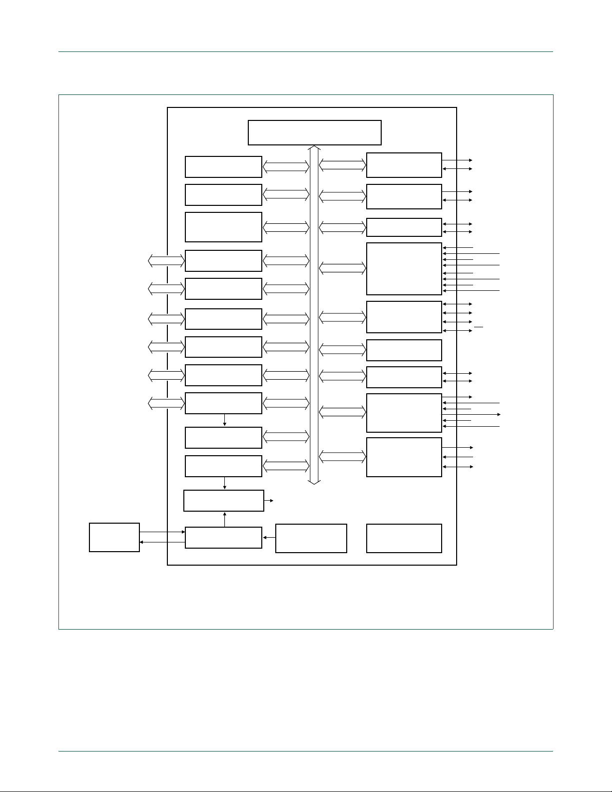
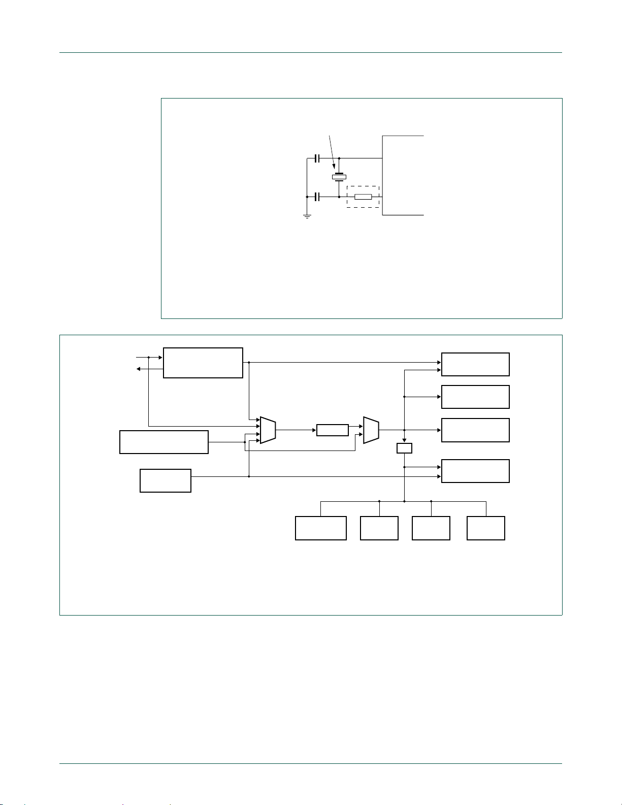
ACCELERATED 2-CLOCK 80C51 CPU
P5[7:0]
P4[7:0]
P3[1:0]
P2[5:0]
P2[7:0]
P1[7:0]
P0[7:0]
8 kB/16 kB
CODE FLASH
256-BYTE
DATA RAM
256-BYTE
AUXILIARY RAM
PORT 5
CONFIGURABLE I/Os
PORT 4
CONFIGURABLE I/Os
PORT 3
CONFIGURABLE I/Os
(1)
(2)
PORT 2
CONFIGURABLE I/Os
PORT 1
CONFIGURABLE I/Os
PORT 0
CONFIGURABLE I/Os
KEYPAD
INTERRUPT
WATCHDOG TIMER
AND OSCILLATOR
internal
bus
UART0
UART1
I2C-BUS
ADC0
SPI
REAL-TIME CLOCK/
SYSTEM TIMER
TIMER 0
TIMER 1
ANALOG
COMPARATORS
DEBUGGER
INTERFACE
TXD0
RXD0
TXD1
RXD1
SCL
SDA
AD00
AD02
AD04
AD06
SPICLK
MOSI
MISO
SS
T0
T1
CMP2
CIN2A
CIN1A
TRIG
TCLK
TDI
AD01
AD03
AD05
AD07
CIN2B
CMP1
CIN1B
CRYSTAL
OR
RESONATOR
XTAL1
XTAL2
PROGRAMMABLE
OSCILLATOR DIVIDER
CONFIGURABLE
OSCILLATOR
CPU
clock
ON-CHIP RC
OSCILLATOR WITH
CLOCK DOUBLER
POWER MONITOR
(POWER-ON RESET,
BROWNOUT RESET)
002aab305
(1) 44-pin package.
(2) 48-pin package.
Fig 4. Block diagram
UM10147_2 © NXP B.V. 2008. All rights reserved.
User manual Rev. 02 — 28 April 2008 10 of 134
Page 11

NXP Semiconductors
1.3 Special function registers
Remark: SFR accesses are restricted in the following ways:
• User must not attempt to access any SFR locations not defined.
• Accesses to any defined SFR locations m ust be strictly for the functions for the SFRs.
• SFR bits labeled ‘-’, ‘0’ or ‘1’ can only be written and read as follows:
UM10147
P89LPC952/954 User manual
– ‘-’ Unless otherwise specified, must be written with ‘0’, but can return any value
when read (even if it was written with ‘0’). It is a reserved bit and may be used in
future derivatives.
– ‘0’ must be written with ‘0’, and will return a ‘0’ when read.
– ‘1’ must be written with ‘1’, and will return a ‘1’ when read.
UM10147_2 © NXP B.V. 2008. All rights reserved.
User manual Rev. 02 — 28 April 2008 11 of 134
Page 12

xxxxxxxxxxxxxxxxxxxxx xxxxxxxxxxxxxxxxxxxxxxxxxx xxxxxxx x x x xxxxxxxxxxxxxxxxxxxxxxxxxxxxxx xxxxxxxxxxxxxxxxxxx xx xx xxxxx
xxxxxxxxxxxxxxxxxxxxxxxxxxx xxxxxxxxxxxxxxxxxxx xxxxxx xxxxxxxxxxxxxxxxxxxxxxxxxxxxxxxxxxx xxxxxxxxxxxx x x
xxxxxxxxxxxxxxxxxxxxx xxxxxxxxxxxxxxxxxxxxxxxxxxxxxx xxxxx xxxxxxxxxxxxxxxxxxxxxxxxxxxxxxxxxxxxxxxxxxxxxxxxxx xxxxxxxx
UM10147_2 © NXP B.V. 2008. All rights reserved.
User manual Rev. 02 — 28 April 2008 12 of 134
Table 2. Special function registers
* indicates SFRs that are bit addressable.
Name Description SFR
ACC* Accumulator E0H 00 0000 0000
AD0CON ADC0 control
AD0INS ADC0 input
AD0MODA ADC0 mode
AD0MODB ADC0 mode
AUXR1 Auxiliary
B* B register F0H 00 0000 0000
BRGR0_0 Baud rate
BRGR1_0 Baud rate
BRGCON_0 Baud rate
CMP1 Comparator 1
CMP2 Comparator 2
DIVM CPU clock
DPTR Data pointer
xxxxxxxxxxxxxxxxxxxxxxxxx xxxxxxxxxxxxxxxxxxxx xxx
Bit functions and addresses Reset value
addr.
MSB LSB Hex Binary
Bit addressE7E6E5E4E3E2E1E0
97H ENBI0 ENADCI0 TMM0 EDGE0 ADCI0 ENADC0 ADCS01 ADCS00 00 0000 0000
register
A3H ADI07 ADI06 ADI05 ADI04 ADI03 ADI02 ADI01 ADI00 00 0000 0000
select
C0HBNDI0BURST0SCC0SCAN0----0000000000
register A
A1HCLK2CLK1CLK0-----00000x0000
register B
A2H CLKLP EBRR ENT1 ENT0 SRST 0 - DPS 00 0000 00x0
function
register
Bit addressF7F6F5F4F3F2F1F0
BEH 00 0000 0000
generator 0
rate low
BFH 00 0000 0000
generator 0
rate high
BDH------SBRGS_0BRGEN_000
generator 0
control
ACH - - CE1 CP1 CN1 OE1 CO1 CMF1 00
control register
ADH - - CE2 CP2 CN2 OE2 CO2 CMF2 00
control register
95H 00 0000 0000
divide-by-M
control
(2 bytes)
[2]
[1]
[1]
xxxx xx00
xx00 0000
xx00 0000
NXP Semiconductors
P89LPC952/954 User manual
UM10147
Page 13

xxxxxxxxxxxxxxxxxxxxx xxxxxxxxxxxxxxxxxxxxxxxxxx xxxxxxx x x x xxxxxxxxxxxxxxxxxxxxxxxxxxxxxx xxxxxxxxxxxxxxxxxxx xx xx xxxxx
xxxxxxxxxxxxxxxxxxxxxxxxxxx xxxxxxxxxxxxxxxxxxx xxxxxx xxxxxxxxxxxxxxxxxxxxxxxxxxxxxxxxxxx xxxxxxxxxxxx x x
xxxxxxxxxxxxxxxxxxxxx xxxxxxxxxxxxxxxxxxxxxxxxxxxxxx xxxxx xxxxxxxxxxxxxxxxxxxxxxxxxxxxxxxxxxxxxxxxxxxxxxxxxx xxxxxxxx
UM10147_2 © NXP B.V. 2008. All rights reserved.
User manual Rev. 02 — 28 April 2008 13 of 134
Table 2. Special function registers
* indicates SFRs that are bit addressable.
Name Description SFR
DPH Data pointer
DPL Data poi n te r
FMADRH Program flash
FMADRL Program flash
FMCON Program flash
FMDATA Program flash
I2ADR I
I2CON* I
I2DAT I
I2SCLH Serial clock
I2SCLL Serial clock
I2STAT I
xxxxxxxxxxxxxxxxxxxxxxxxx xxxxxxxxxxxxxxxxxxxx xxx
high
low
address high
address low
control (Read)
Program flash
control (Write)
data
2
C-bus slave
address
register
Bit address DF DE DD DC DB DA D9 D8
2
C-bus control
register
2
C-bus data
register
generator/SCL
duty cycle
register high
generator/SCL
duty cycle
register low
2
C-bus status
register
Bit address AF AE AD AC AB AA A9 A8
…continued
Bit functions and addresses Reset value
addr.
83H 00 0000 0000
82H 00 0000 0000
E7H 00 0000 0000
E6H 00 0000 0000
E4H BUSY - - - HVA HVE SV OI 70 0111 0000
E4H FMCMD.7 FMCMD.6 FMCMD.5 FMCMD.4 FMCMD.3 FMCMD.2 FMCMD.1 FMCMD.0
E5H 00 0000 0000
DBH I2ADR.6 I2ADR.5 I2ADR.4 I2ADR.3 I2ADR.2 I2ADR.1 I2ADR.0 GC 00 0000 0000
D8H - I2EN STA STO SI AA - CRSEL 00 x000 00x0
DAH
DDH 00 0000 0000
DCH 00 0000 0000
D9H STA.4 STA.3 STA.2 STA.1 STA.0 0 0 0 F8 11111000
MSB LSB Hex Binary
NXP Semiconductors
P89LPC952/954 User manual
UM10147
Page 14

xxxxxxxxxxxxxxxxxxxxx xxxxxxxxxxxxxxxxxxxxxxxxxx xxxxxxx x x x xxxxxxxxxxxxxxxxxxxxxxxxxxxxxx xxxxxxxxxxxxxxxxxxx xx xx xxxxx
xxxxxxxxxxxxxxxxxxxxxxxxxxx xxxxxxxxxxxxxxxxxxx xxxxxx xxxxxxxxxxxxxxxxxxxxxxxxxxxxxxxxxxx xxxxxxxxxxxx x x
xxxxxxxxxxxxxxxxxxxxx xxxxxxxxxxxxxxxxxxxxxxxxxxxxxx xxxxx xxxxxxxxxxxxxxxxxxxxxxxxxxxxxxxxxxxxxxxxxxxxxxxxxx xxxxxxxx
UM10147_2 © NXP B.V. 2008. All rights reserved.
User manual Rev. 02 — 28 April 2008 14 of 134
Table 2. Special function registers …continued
* indicates SFRs that are bit addressable.
Name Description SFR
IEN0* Interrupt
IEN1* Interrupt
IEN2 Interrupt
IP0* Interrupt
IP0H Interrupt
IP1* Interrupt
IP1H Interrupt
IP2 Interrupt
IP2H Interrupt
KBCON Keypad control
KBMASK Keypad
KBPA TN Keypad pattern
P0* Port 0 80H T1/KB7 CMP1
P1* Port 1 90H - - RST
xxxxxxxxxxxxxxxxxxxxxxxxx xxxxxxxxxxxxxxxxxxxx xxx
Bit functions and addresses Reset value
addr.
A8H EA EWDRT EBO ES/ESR ET1 EX1 ET0 EX0 00 0000 0000
enable 0
Bit address EF EE ED EC EB EA E9 E8
E8H - EST - - ESPI EC EKBI EI2C 00
enable 1
D5H - - - - EST1 ES1/ESR1 EADC - 00
enable 2
Bit address BF BE BD BC BB BA B9 B8
B8H - PWDRT PBO PS/PSR PT1 PX1 PT0 PX0 00
priority 0
B7H - PWDRTH PBOH PSH/
priority 0 high
Bit address FF FE FD FC FB FA F9 F8
F8H - PST - - PSPI PC PKBI PI2C 00
priority 1
F7H - PSTH - - PSPIH PCH PKBIH PI2CH 00
priority 1 high
D6H - - - - PEST1 PES1/
priority 2
D7H - - - - PEST1H PES1H/
priority 2 high
94H------PATN
register
86H 00 0000 0000
interrupt mask
register
93H FF 1111 1111
register
Bit address8786858483828180
Bit address9796959493929190
MSB LSB Hex Binary
/KB6
CMPREF
/KB5
PT1H PX1H PT0H PX0H 00
PSRH
PADC - 00
PESR1
PADCH - 00
PESR1H
KBIF 00
_SEL
CIN1A
/KB4
CIN1B
/KB3
CIN2A
/KB2
CIN2B
/KB1
CMP2
/KB0
INT1 INT0/SDA T0/SCL RXD0 TXD0
NXP Semiconductors
[1]
00x0 0000
[1]
00x0 0000
[1]
x000 0000
[1]
x000 0000
[1]
00x0 0000
[1]
00x0 0000
[1]
00x0 0000
[1]
00x0 0000
[1]
xxxx xx00
P89LPC952/954 User manual
UM10147
[1]
[1]
Page 15

xxxxxxxxxxxxxxxxxxxxx xxxxxxxxxxxxxxxxxxxxxxxxxx xxxxxxx x x x xxxxxxxxxxxxxxxxxxxxxxxxxxxxxx xxxxxxxxxxxxxxxxxxx xx xx xxxxx
xxxxxxxxxxxxxxxxxxxxxxxxxxx xxxxxxxxxxxxxxxxxxx xxxxxx xxxxxxxxxxxxxxxxxxxxxxxxxxxxxxxxxxx xxxxxxxxxxxx x x
xxxxxxxxxxxxxxxxxxxxx xxxxxxxxxxxxxxxxxxxxxxxxxxxxxx xxxxx xxxxxxxxxxxxxxxxxxxxxxxxxxxxxxxxxxxxxxxxxxxxxxxxxx xxxxxxxx
UM10147_2 © NXP B.V. 2008. All rights reserved.
User manual Rev. 02 — 28 April 2008 15 of 134
Table 2. Special function registers …continued
* indicates SFRs that are bit addressable.
Name Description SFR
P2* Port 2 A0H - - SPICLK SS
P3*Port3B0H------XTAL1XTAL2
P4 Port 4 B3H - TMS - - RXD1 TXD1 TRIG T3EX
P5Port5B4HT3------P0M1 Port 0 output
P0M2 Port 0 output
P1M1 Port 1 output
P1M2 Port 1 output
P2M1 Port 2 output
P2M2 Port 2 output
P3M1 Port 3 output
P3M2 Port 3 output
PCON Power control
PCONA Power control
PSW* Program status
PT0AD Port 0 digital
RSTSRC Reset source
xxxxxxxxxxxxxxxxxxxxxxxxx xxxxxxxxxxxxxxxxxxxx xxx
Bit functions and addresses Reset value
addr.
Bit address9796959493929190
Bit addressB7B6B5B4B3B2B1B0
84H (P0M1.7) (P0M1.6) (P0M1.5) (P0M1.4) (P0M1.3) (P0M1.2) (P0M1.1) (P0M1.0) FF
mode 1
85H (P0M2.7) (P0M2.6) (P0M2.5) (P0M2.4) (P0M2.3) (P0M2.2) (P0M2.1) (P0M2.0) 00
mode 2
91H (P1M1.7) (P1M1.6) - (P1M1.4) (P1M1.3) (P1M1.2) (P1M1.1) (P1M1.0) D3
mode 1
92H (P1M2.7) (P1M2.6) - (P1M2.4) (P1M2.3) (P1M2.2) (P1M2.1) (P1M2.0) 00
mode 2
A4H - - (P2M1.5) (P2M1.4) (P2M1.3) (P2M1.2) (P2M1.1) (P2M1.0) FF
mode 1
A5H - - (P2M2.5) (P2M2.4) (P2M2.3) (P2M2.2) (P2M2.1) (P2M2.0) 00
mode 2
B1H------(P3M1.1)(P3M1.0)03xxxx xx11
mode 1
B2H------(P3M2.1)(P3M2.0)00
mode 2
87H SMOD1 SMOD0 BOPD BOI GF1 GF0 PMOD1 PMOD0 00 0000 0000
register
B5H RTCPD - VCPD ADPD I2PD SPPD SPD - 00
register A
Bit addressD7D6D5D4D3D2D1D0
D0H CY AC F0 RS1 RS0 OV F1 P 00 0000 0000
word
F6H - - PT0AD.5 PT0AD.4 PT0AD.3 PT0AD.2 PT0AD.1 - 00 xx00 000x
input disable
DFH - - BOF POF R_BK R_WD R_SF R_EX
register
MSB LSB Hex Binary
MISO MOSI - -
NXP Semiconductors
[1]
[1]
[1]
[1]
[1]
1111 1111
[1]
0000 0000
[1]
11x1 xx11
[1]
00x0 xx00
[1]
1111 1111
[1]
0000 0000
[1]
xxxx xx00
P89LPC952/954 User manual
[1]
0000 0000
UM10147
[3]
Page 16

xxxxxxxxxxxxxxxxxxxxx xxxxxxxxxxxxxxxxxxxxxxxxxx xxxxxxx x x x xxxxxxxxxxxxxxxxxxxxxxxxxxxxxx xxxxxxxxxxxxxxxxxxx xx xx xxxxx
xxxxxxxxxxxxxxxxxxxxxxxxxxx xxxxxxxxxxxxxxxxxxx xxxxxx xxxxxxxxxxxxxxxxxxxxxxxxxxxxxxxxxxx xxxxxxxxxxxx x x
xxxxxxxxxxxxxxxxxxxxx xxxxxxxxxxxxxxxxxxxxxxxxxxxxxx xxxxx xxxxxxxxxxxxxxxxxxxxxxxxxxxxxxxxxxxxxxxxxxxxxxxxxx xxxxxxxx
UM10147_2 © NXP B.V. 2008. All rights reserved.
User manual Rev. 02 — 28 April 2008 16 of 134
Table 2. Special function registers
* indicates SFRs that are bit addressable.
Name Description SFR
RTCCON RTC control D1H RTCF RTCS1 RTCS0 - - - ERTC RTCEN 60
RTCH RTC register
RTCL RTC register
S0ADDR Serial port
S0ADEN Serial port
S0BUF Serial Port data
S0CON* Serial port
S0STAT Serial port
SP Stack pointer 81H 07 0000 0111
SPCTL SPI control
SPSTAT SPI status
SPDAT SPI data
S1CON Serial port 1
S1STAT Serial port 1
TAMOD Timer 0 and 1
xxxxxxxxxxxxxxxxxxxxxxxxx xxxxxxxxxxxxxxxxxxxx xxx
…continued
Bit functions and addresses Reset value
addr.
D2H 00
high
D3H 00
low
A9H 00 0000 0000
address
register
B9H 00 0000 0000
address enable
99H xx xxxx xxxx
buffer register
Bit address 9F 9E 9D 9C 9B 9A 99 98
98H SM0_0/FE_0SM1_00 SM2_0 REN_0 TB8_0 RB8_0 TI_0 RI_0 00 0000 0000
control
BAH DBMOD_0 INTLO_0 CIDIS_0 DBISEL_0 FE_0 BR_0 OE_0 STINT_0 00 0000 0000
extended
status register
E2H SSIG SPEN DORD MSTR CPOL CPHA SPR1 SPR0 04 0000 0100
register
E1HSPIFWCOL------0000xxxxxx
register
E3H 00 0000 0000
register
B6H SM0_1/FE_1SM1_1 SM2_1 REN_1 TB8_1 RB8_1 TI_1 RI_1 00 0000 0000
control
D4H DBMOD_1 INTLO_1 CIDIS_1 DBISEL_1 FE_1 BR_1 OE_1 STINT_1 00 0000 0000
extended
status register
8FH - - - T1M2 - - - T0M2 00 xxx0 xxx0
auxiliary mode
Bit address 8F 8E 8D 8C 8B 8A 89 88
MSB LSB Hex Binary
[1][6]
[6]
[6]
NXP Semiconductors
011x xx00
0000 0000
0000 0000
P89LPC952/954 User manual
UM10147
Page 17

xxxxxxxxxxxxxxxxxxxxx xxxxxxxxxxxxxxxxxxxxxxxxxx xxxxxxx x x x xxxxxxxxxxxxxxxxxxxxxxxxxxxxxx xxxxxxxxxxxxxxxxxxx xx xx xxxxx
xxxxxxxxxxxxxxxxxxxxxxxxxxx xxxxxxxxxxxxxxxxxxx xxxxxx xxxxxxxxxxxxxxxxxxxxxxxxxxxxxxxxxxx xxxxxxxxxxxx x x
xxxxxxxxxxxxxxxxxxxxx xxxxxxxxxxxxxxxxxxxxxxxxxxxxxx xxxxx xxxxxxxxxxxxxxxxxxxxxxxxxxxxxxxxxxxxxxxxxxxxxxxxxx xxxxxxxx
UM10147_2 © NXP B.V. 2008. All rights reserved.
User manual Rev. 02 — 28 April 2008 17 of 134
Table 2. Special function registers
* indicates SFRs that are bit addressable.
Name Description SFR
TCON* Timer 0 and 1
TH0 Timer 0 high 8CH 00 0000 0000
TH1 Timer 1 high 8DH 00 0000 0000
TL0 Timer 0 low 8AH 00 0000 0000
TL1 Timer 1 low 8BH 00 0000 0000
TMOD Timer 0 and 1
TRIM Internal
WDCON Watchdog
WDL Watchdog load C1H FF 1111 1111
WFEED1 Watchdog
WFEED2 Watchdog
xxxxxxxxxxxxxxxxxxxxxxxxx xxxxxxxxxxxxxxxxxxxx xxx
…continued
Bit functions and addresses Reset value
addr.
88H TF1 TR1 TF0 TR0 IE1 IT1 IE0 IT0 00 0000 0000
control
89H T1GATE T1C/T T1M1 T1M0 T0GATE T0C/T T0M1 T0M0 00 0000 0000
mode
96H RCCLK ENCLK TRIM.5 TRIM.4 TRIM.3 TRIM.2 TRIM.1 TRIM.0
oscillator trim
register
A7H PRE2 PRE1 PRE0 - - WDRUN WDTOF WDCLK
control register
C2H
feed 1
C3H
feed 2
MSB LSB Hex Binary
[5] [6]
[4] [6]
NXP Semiconductors
[1] All ports are in input only (high-impedance) state after power-up.
[2] BRGR1_0 and BRGR0_0 must only be written if BRGEN_0 in BRGCON_0 SFR is logic 0. If any are written while BRGEN_0 = 1, the result is unpredictable.
[3] The RSTSRC register reflects the cause of the UM10147 reset. Upon a power-up reset, all reset source flags are cleared except POF and BOF; the power-on reset value is
xx110000.
[4] After reset, the value is 1110 01x1, i.e., PRE2 to PRE0 are all logic 1, WDRUN = 1 and WDCLK = 1. WDTOF bit is logic 1 after watchdog reset and is logic 0 after power-on reset.
Other resets will not affect WDTOF.
[5] On power-on reset, the TRIM SFR is initialized with a factory preprogrammed value. Other resets will not cause initialization of the TRIM register.
[6] The only reset source that affects these SFRs is power-on reset.
P89LPC952/954 User manual
UM10147
Page 18

xxxxxxxxxxxxxxxxxxxxx xxxxxxxxxxxxxxxxxxxxxxxxxx xxxxxxx x x x xxxxxxxxxxxxxxxxxxxxxxxxxxxxxx xxxxxxxxxxxxxxxxxxx xx xx xxxxx
xxxxxxxxxxxxxxxxxxxxxxxxxxx xxxxxxxxxxxxxxxxxxx xxxxxx xxxxxxxxxxxxxxxxxxxxxxxxxxxxxxxxxxx xxxxxxxxxxxx x x
xxxxxxxxxxxxxxxxxxxxx xxxxxxxxxxxxxxxxxxxxxxxxxxxxxx xxxxx xxxxxxxxxxxxxxxxxxxxxxxxxxxxxxxxxxxxxxxxxxxxxxxxxx xxxxxxxx
UM10147_2 © NXP B.V. 2008. All rights reserved.
User manual Rev. 02 — 28 April 2008 18 of 134
Table 3. Extended special function registers
Name Description SFR
ADC0HBND ADC0 high_boundary register,
ADC0LBND ADC0 low_boundary register
AD0DAT0R ADC0 data register 0, right
AD0DAT0L ADC0 data register 0, left
AD0DAT1R ADC0 data register 1, right
AD0DAT1L ADC0 data register 1, left
AD0DAT2R ADC0 data register 2, right
AD0DAT2L ADC0 data register 2, left
AD0DAT3R ADC0 data register 3, right
AD0DAT3L ADC0 data register 3, left
AD0DAT4R ADC0 data register 4, right
AD0DAT4L ADC0 data register 4, left
AD0DAT5R ADC0 data register 5, right
AD0DAT5L ADC0 data register 5, left
AD0DAT6R ADC0 data register 6, right
AD0DAT6L ADC0 data register 6, left
AD0DAT7R ADC0 data register 7, right
xxxxxxxxxxxxxxxxxxxxxxxxx xxxxxxxxxxxxxxxxxxxx xxx
left (MSB)
(MSB)
(LSB)
(MSB)
(LSB)
(MSB)
(LSB)
(MSB)
(LSB)
(MSB)
(LSB)
(MSB)
(LSB)
(MSB)
(LSB)
(MSB)
(LSB)
Bit functions and addresses Reset value
addr.
FFEFH FF 1111 1111
FFEEH 00 0000 0000
FFFEH AD0DAT0[7:0] 00 0000 0000
FFFFH AD0DAT0[9:2] 00 0000 0000
FFFCH AD0DAT1[7:0] 00 0000 0000
FFFDH AD0DAT1[9:2] 00 0000 0000
FFFAH AD0DAT2[7:0] 00 0000 0000
FFFBH AD0DAT2[9:2] 00 0000 0000
FFF8H AD0DAT3[7:0] 00 0000 0000
FFF9H AD0DAT3[9:2] 00 0000 0000
FFF6H AD0DAT4[7:0] 00 0000 0000
FFF7H AD0DAT4[9:2] 00 0000 0000
FFF4H AD0DAT5[7:0] 00 0000 0000
FFF5H AD0DAT5[9:2] 00 0000 0000
FFF2H AD0DAT6[7:0] 00 0000 0000
FFF3H AD0DAT6[9:2] 00 0000 0000
FFF0H AD0DAT7[7:0]
MSB LSB Hex Binary
NXP Semiconductors
P89LPC952/954 User manual
UM10147
Page 19

xxxxxxxxxxxxxxxxxxxxx xxxxxxxxxxxxxxxxxxxxxxxxxx xxxxxxx x x x xxxxxxxxxxxxxxxxxxxxxxxxxxxxxx xxxxxxxxxxxxxxxxxxx xx xx xxxxx
xxxxxxxxxxxxxxxxxxxxxxxxxxx xxxxxxxxxxxxxxxxxxx xxxxxx xxxxxxxxxxxxxxxxxxxxxxxxxxxxxxxxxxx xxxxxxxxxxxx x x
xxxxxxxxxxxxxxxxxxxxx xxxxxxxxxxxxxxxxxxxxxxxxxxxxxx xxxxx xxxxxxxxxxxxxxxxxxxxxxxxxxxxxxxxxxxxxxxxxxxxxxxxxx xxxxxxxx
UM10147_2 © NXP B.V. 2008. All rights reserved.
User manual Rev. 02 — 28 April 2008 19 of 134
Table 3. Extended special function registers
Name Description SFR
AD0DAT7L ADC0 data register 7, left
BNDSTA0 ADC0 boundary status register FFEDH
BRGCON_1 Baud rate generator 1 control FFB3H - - - - - - SBRGS_1BRGEN_100
BRG0_1 Baud rate generator 1 rate low FFB4H
BRG1_1 Baud rate generator 1 rate high FFB5H
FREEZE Peripheral clock freeze FFD0H - - - RTC_F - WDT_F T1_F T0_F 00 xxx0 0000
P4M1 Port 4 output mode 1 FFB8H (P4M1.7) (P4M1.6) (P4M1.5) (P4M1.4) (P4M1.3) (P4M1.2) (P4M1.1) (P4M1.0) FF
P4M2 Port 4 output mode 2 FFB9H (P4M2.7) (P4M2.6) (P4M2.5) (P4M2.4) (P4M2.3) (P4M2.2) (P4M2.1) (P4M2.0) 00
P5M1 Port 5 output mode 1 FFBAH (P5M1.7) (P5M1.6) (P5M1.5) (P5M1.4) (P5M1.3) (P5M1.2) (P5M1.1) (P5M1.0) FF
P5M2 Port 5 output mode 3 FFBBH (P5M2.7) (P5M2.6) (P5M2.5) (P5M2.4) (P5M2.3) (P5M2.2) (P5M2.1) (P5M2.0) 00
S1ADDR Serial port 1 address register FFB2H 00 0000 0000
S1ADEN Serial port 1 address enable FFB1H 00 0000 0000
S1BUF Serial port 1 data buffer
xxxxxxxxxxxxxxxxxxxxxxxxx xxxxxxxxxxxxxxxxxxxx xxx
…continued
Bit functions and addresses Reset value
addr.
FFF1H AD0DAT7[9:2]
(MSB)
FFB0H xx xxxx xxxx
register
MSB LSB Hex Binary
[2]
xxxx xx00
[1]
1111 1111
[1]
0000 0000
[1]
1111 1111
[1]
0000 0000
NXP Semiconductors
[1] Extended SFRs are physically located on-chip but logically located in external data memory address space (XDATA). The MOVX A,@DPTR and MOVX @DPTR,A instructions are
used to access these extended SFRs.
[2] BRGR1_1 and BRGR0_1 must only be written if BRGEN_1 in BRGCON_1 SFR is logic 0. If any are written while BRGEN_1 = 1, the result is unpredictable.
P89LPC952/954 User manual
UM10147
Page 20
NXP Semiconductors
1.4 Memory organization
FF00h
FFEFh
1FFFh
1E00h
1C00h
1BFFh
1800h
17FFh
1400h
13FFh
1000h
0FFFh
0C00h
0BFFh
0800h
07FFh
0400h
03FFh
0000h
IAP entry-
points
ISP CODE
(512B)*
SECTOR 7
SECTOR 6
SECTOR 5
SECTOR 4
SECTOR 3
SECTOR 2
SECTOR 1
SECTOR 0
Read-protected
IAP calls only
IDATA routines
entry points for:
-51 ASM. code
-C code
ISP serial loader
entry points for:
-UART (auto-baud)
-I2C, SPI, etc.*
Flexible choices:
-as supplied (UART)
-Philips libraries*
-user-defined
FFEFh
FF1Fh
FF00h
1FFFh
1E00h
entry
points
SPECIAL FUNCTION
REGISTERS
(DIRECTLY ADDRESSABLE)
UM10147
P89LPC952/954 User manual
IDATA (incl. DATA)
128 BYTES ON-CHIP
DATA MEMORY (STACK
AND INDIR. ADDR.)
DATA
128 BYTES ON-CHIP
DATA MEMORY (STACK,
DIRECT AND INDIR. ADDR.)
4 REG. BANKS R[7:0]
data memory
(DATA, IDATA)
002aaa948
Fig 5. P89LPC952 memory map - P89LPC954 is similar
The various P89LPC952/954 memory spaces are as follows:
DATA — 128 bytes of internal data memory space (00h:7Fh) accessed via direct or
indirect addressing, using instruction other than MOVX and MOVC. All or part of the Stack
may be in this area.
IDATA — Indirect Data. 256 bytes of internal data memory space (00h:FFh) accessed via
indirect addressing using instructions other than MOVX and MOVC. All or part of the
Stack may be in this area. This area includes the DATA area and the 128 bytes
immediately above it.
SFR — Special Function Registers. Sele cted CPU registers and peripheral control and
status registers, accessible only via direct addressing.
XDATA — ‘External’ Data or Auxiliary RAM. Duplicates the classic 80C51 64 kB memory
space addressed via the MOVX instruction using the DPTR, R0, or R1. All or part of this
space could be implemented on-chip. The P89LPC952/954 has 256 bytes of on-chip
XDATA memory.
CODE — 64 kB of Code memory space, accessed as part of program execution and via
the MOVC instruction. The P89LPC952/954 has 8 kB/ 16 kB of on-chip Code memory.
Table 4. Data RAM arrangement
Type Data RAM Size (bytes)
DATA Directl y an d indirectly addressable memory 128
IDATA Indirectly addressable memory 256
XDATA Indirectly addressable using MOVX, MOVC, DPTR, R0, R1 256
UM10147_2 © NXP B.V. 2008. All rights reserved.
User manual Rev. 02 — 28 April 2008 20 of 134
Page 21

NXP Semiconductors
The P89LPC952/954 is a single-chip microcontroller designed for applications demanding
high-integration, low cost solutions over a wide range of performance requirements. The
P89LPC952/954 is based on a high performance processor architecture that executes
instructions in two to four clocks, six times the rate of standard 80C51 devices. Many
system-level functions have been incorporated into the P89LPC952/954 in order to
reduce component count, board space, and system cost
UM10147
P89LPC952/954 User manual
UM10147_2 © NXP B.V. 2008. All rights reserved.
User manual Rev. 02 — 28 April 2008 21 of 134
Page 22

NXP Semiconductors
2. Clocks
2.1 Enhanced CPU
The P89LPC952/954 uses an enhanced 80C51 CPU which ru ns at six times the spee d of
standard 80C51 devices. A machine cycle consists of two CPU clock cycles, and most
instructions execute in one or two machine cycles.
2.2 Clock definitions
The P89LPC952/954 device has several internal clocks as defined below:
OSCCLK — Input to the DIVM clock divider. OSCCLK is selected from one of four clock
sources and can also be optionally divided to a slower frequency (see Figure 6
Section 2.8 “
OSCCLK frequency.
CCLK — CPU clock; output of the DIVM clock divider. There are two CCLK cycles per
machine cycle, and most instructions are executed in one to two machine cycles (two or
four CCLK cycles).
RCCLK — The internal 7.373 MHz RC oscillator output.
PCLK — Clock for the various peripheral devices and is
P89LPC952/954 User manual
CPU Clock (CCLK) modification: DIVM register”). Note: f
CCLK
⁄
.
2
UM10147
and
is defined as the
osc
2.2.1 Oscillator Clock (OSCCLK)
The P89LPC952/954 provides several user-selectable oscillator options. This allows
optimization for a range of needs from high precision to lowest possible cost. These
options are configured when the FLASH is programmed and include an on -chip watchdog
oscillator, an on-chip RC oscillator, an oscillator using an external crystal, or an external
clock source. The crystal oscillator can be optimized for low, medium, or high frequency
crystals covering a range from 20 kHz to 18 MHz.
2.2.2 Low speed oscillator option
This option supports an external crystal in the range of 20 kHz to 100 kHz. Ceramic
resonators are also supported in this configuration.
2.2.3 Medium speed oscillator option
This option supports an external crystal in the range of 100 kHz to 4 MHz. Ceramic
resonators are also supported in this configuration.
2.2.4 High speed oscillator option
This option supports an external crystal in the range of 4 MHz to 18 MHz. Ceramic
resonators are also supported in this configuration. When using a clock frequency
above 12 MHz, the reset input function of P1.5 must be enabled. An external circuit
is required to hold the device in reset at power-up until V
specified level. When system power is removed V
specified operating voltage. When using a clock frequency above 12 MHz, in some
applications, an external brownout detect circuit may be required to hold the device
in reset when V
requirements for clock frequencies above 12 MHz do not apply when using the
internal RC oscillator in clock doubler mode.
falls below the minimum specified operating voltage. These
DD
has reached its
DD
will fall below the minimum
DD
UM10147_2 © NXP B.V. 2008. All rights reserved.
User manual Rev. 02 — 28 April 2008 22 of 134
Page 23

NXP Semiconductors
2.3 Clock output
The P89LPC952/954 supports a user-selectable clock output function on the XTAL2 /
CLKOUT pin when the crystal oscillator is not being used. This condition occurs if a
different clock source has been selected (on-chip RC oscillator, watchdog oscillator,
external clock input on X1) and if the Real-time Clock is not using the crystal oscillator as
its clock source. This allows external devices to synchronize to the P89LPC9 52/954 . This
output is enabled by the ENCLK bit in the TRIM register
UM10147
P89LPC952/954 User manual
The frequency of this clock output is
1
⁄
that of the CCLK. If the clock output is not needed
2
in Idle mode, it may be turned off prior to entering Idle, saving additional power. Note: on
reset, the TRIM SFR is initialized with a factory preprogrammed value. Therefore when
setting or clearing the ENCLK bit, the user should retain the contents of other bits of the
TRIM register. This can be done by reading the contents of the TRIM register (into the
ACC for example), modifying bit 6, and writing this result back into the TRIM register.
Alternatively, the ‘ANL direct’ or ‘ORL direct’ instructions can be used to clear or set bit 6
of the TRIM register.
2.4 On-chip RC oscillator option
The P89LPC952 has a 6-bit TRIM register that can be used to tune the frequency of the
RC oscillator. During reset, the TRIM value is initialized to a factory pre-programmed
value to adjust the oscillator frequency to 7.373 MHz ± 1 % at room temperature. (Note:
the initial value is better than 1 %; please refer to the P89LPC952/954 data sheet for
behavior over temperature). End user applications can write to the TRIM register to adjust
the on-chip RC oscillator to other frequencies. Increasing the TRIM value will decrease
the oscillator frequency. When the clock doubler option is enabled (UCFG1.3 = 1), the
output frequency is doubled. If CCLK is 8 MHz or slower, the CLKLP SFR bit (AUXR1.7)
can be set to logic 1 to reduce power consumption. On reset, CLKLP is logic 0 allowing
highest performance access. This bit can then be se t in software if CCLK is runni ng at
8 MHz or slower.
The requirements in Section 2.2.4 “
an external reset input and using an external reset circuit when the clock freq uency is
greater than 12 MHz do not apply when using the internal RC oscillator’s clock doubler
option.
Table 5. On-chip RC oscillator trim register (TRIM - address 96h) bit allocation
Bit 7 6 5 4 3 2 1 0
Symbol RCCLK ENCLK TRIM.5 TRIM.4 TRIM.3 TRIM.2 TRIM.1 TRIM.0
Reset 0 0 Bits 5:0 loaded with factory stored value during reset.
High speed oscillator option” for configuring P1.5 as
UM10147_2 © NXP B.V. 2008. All rights reserved.
User manual Rev. 02 — 28 April 2008 23 of 134
Page 24

NXP Semiconductors
UM10147
P89LPC952/954 User manual
Table 6. On-chip RC oscillator trim register (TRIM - address 96h) bit description
Bit Symbol Description
0 TRIM.0 Trim value. Determines the frequency of the internal RC oscillator. During reset,
1TRIM.1
2TRIM.2
3TRIM.3
4TRIM.4
5TRIM.5
6 ENCLK when = 1,
7 RCCLK when = 1, selects the RC Oscillator output as the CPU clock (CCLK). This allows for
these bits are loaded with a stored factory calibration value. When writing to either
bit 6 or bit 7 of this register, care should be taken to preserve the current TRIM value
by reading this register, modifying bits 6 or 7 as required, and writing the result to
this register.
CCLK
⁄
is output on the XTAL2 pin provided the crystal oscillator is not
being used.
fast switching between any clock source and the internal RC oscillator without
needing to go through a reset cycle.
2
2.5 Watchdog oscillator option
The watchdog has a separate oscillator which has a frequency of 400 kHz. This oscillator
can be used to save power when a high clock frequency is not needed.
2.6 External clock input option
In this configuration, the processor clock is derived from an external source driving the
XT AL1 / P3.1 pin. The rate may be from 0 Hz up to 18 MHz. The XTAL2 / P3.0 pin may be
used as a standard port pin or a clock output.
When using an external clock input frequency above 12 MHz, the reset input
function of P1.5 must be enabled. An external circuit is required to hold the device
in reset at power-up until V
removed V
will fall below the minimum specified operating voltage. When using
DD
has reached its specified level. When syst em power is
DD
an external clock input frequency above 12 MHz, in some applications, an external
brownout detect circuit may be required to hold the device in reset when V
DD
falls
below the minimum specified operating voltage. These requirements for clock
frequencies above 12 MHz do not apply when using the internal RC oscillator in
clock doubler mode.
UM10147_2 © NXP B.V. 2008. All rights reserved.
User manual Rev. 02 — 28 April 2008 24 of 134
Page 25
NXP Semiconductors
Fig 6. Using the crystal oscillator.
UM10147
P89LPC952/954 User manual
quartz crystal or
ceramic resonator
P89LPC952/954
XTAL1
(1)
XTAL2
002aad364
Note: The oscillator must be configured in one of the following modes: Low frequency crystal,
medium frequency crystal, or high frequency crystal.
(1) A series resistor may be required to limit crystal drive levels. This is especially important for low
frequency crystals (see text).
XTAL1
XTAL2
RC OSCILLATOR
WITH CLOCK DOUBLER
(7.3728 MHz/14.7456 MHz ± 1 %)
(400 kHz +30 % −20 %)
HIGH FREQUENCY
MEDIUM FREQUENCY
LOW FREQUENCY
WATCHDOG
OSCILLATOR
RCCLK
OSCCLK
TIMER 0 AND
DIVM
TIMER 1
RCCLK
PCLK
RTC
ADC0
CCLK
÷2
PCLK
SPI
CPU
WDT
UARTSI2C-BUS
002aab409
Note: The oscillator must be configured in one of the following modes: Low frequency crystal, medium frequency crystal, or high
frequency crystal.
(1) A series resistor may be required to limit crystal drive levels. This is especially important for low frequency crystals (see text).
Fig 7. Block diagram of oscillator control.
2.7 Oscillator Clock (OSCCLK) wake-up delay
The P89LPC952/954 has an internal wake-up timer that delays the clock until it stabilizes
depending to the clock source used. If the clock source is any of the three crystal
selections, the delay is 992 OSCCLK cycles plus 60 μs to 100 μs. If the clock source is
either the internal RC oscillator or the Watchdog oscillator, the delay is 224 OSCCLK
cycles plus 60 μs to 100 μs.
UM10147_2 © NXP B.V. 2008. All rights reserved.
User manual Rev. 02 — 28 April 2008 25 of 134
Page 26

NXP Semiconductors
2.8 CPU Clock (CCLK) modification: DIVM register
The OSCCLK frequency can be divided down, by an integer, up to 510 times by
configuring a dividing register, DIVM, to provide CCLK. This produces the CCLK
frequency using the following formula:
UM10147
P89LPC952/954 User manual
Where: f
Since N ranges from 0 to 255, the CCLK frequency can be in the range of f
(for N = 0, CCLK = f
This feature makes it possible to temporarily run the CPU at a lower rate, reducing power
consumption. By dividing the clock, the CPU can retain the ability to respond to events
other than those that can cause interrupts (i.e. events that allow exiting the Idle mode) by
executing its normal program at a lower rate. This can often result in lower power
consumption than in Idle mode. This can allow bypassing the oscillator start-up time in
cases where Power-down mode would otherwise be used. The value of DIVM may be
changed by the program at any time without interrupting code execution.
2.9 Low power select
The P89LPC952/954 is designed to run at 18 MHz (CCLK) maximum. However, if CCLK
is 8 MHz or slower, the CLKLP SFR bit (AUXR1.7) can be set to a logic 1 to lower the
power consumption further. On any reset, CLKLP is logic 0 allowing highest performance.
This bit can then be set in software if CCLK is running at 8 MHz or slower.
3. A/D converter
CCLK frequency = f
is the frequency of OSCCLK, N is the value of DIVM.
osc
osc
osc
).
/ (2N)
osc
to f
osc
/510.
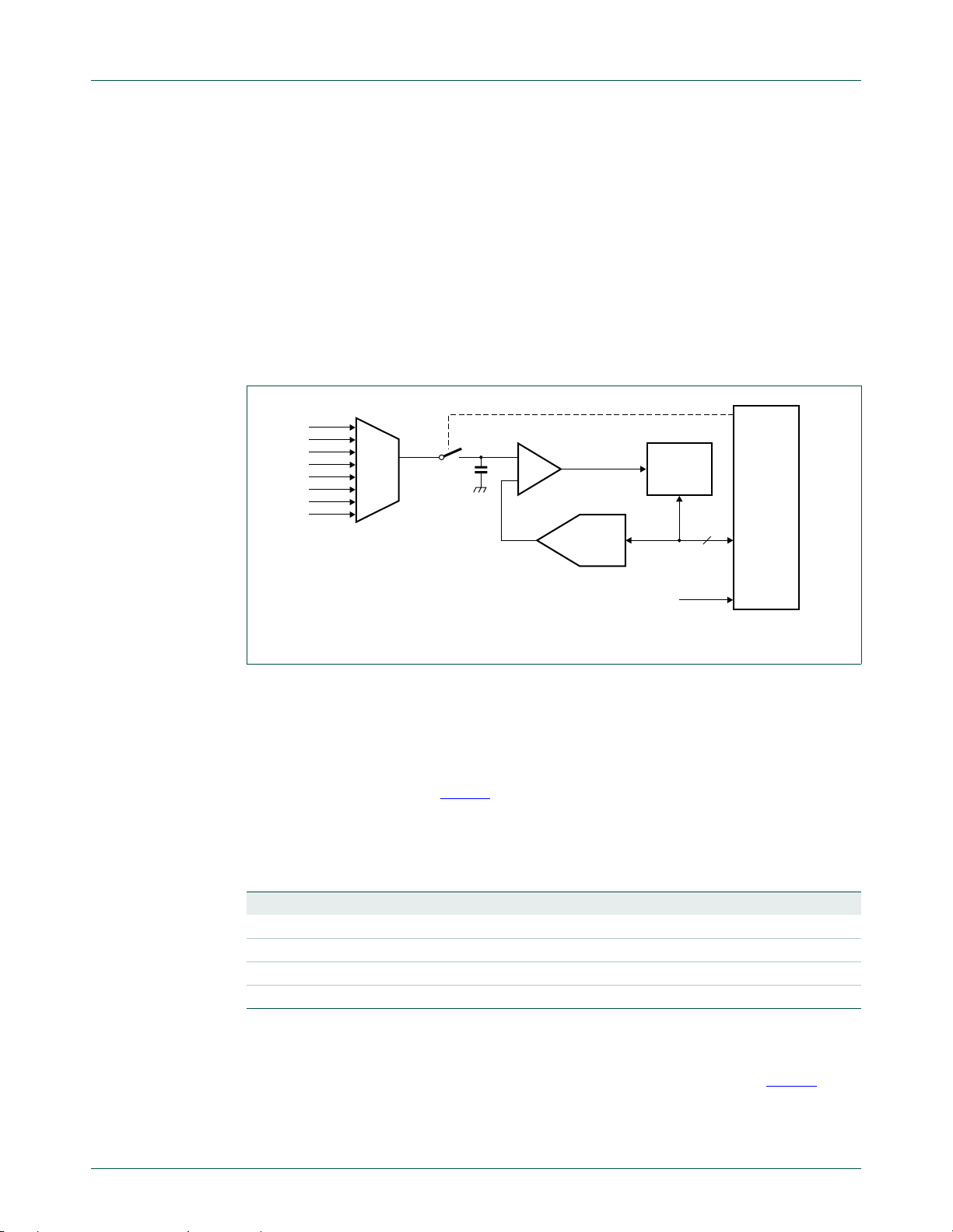
3.1 General description
The P89LPC952/954 has a 10-bit, 8-channel multiplexed successive approximation
analog-to-digital converter module. A block diagram of the A/D converter is shown in
Figure 8
providing an input signal to one of two comp arator inpu ts. The contro l logic in combinati on
with the SAR drives a digital-to-analog converter which provides the other input to the
comparator. The output of the comparator is fed to the SAR.
. The A/D consists of an 8-input multiplexer which feeds a sample-and-hold circuit
3.2 A/D features
• 10-bit, 8-channel multiplexed input, successive approximation A/D converter.
• Eight result register pairs.
• Six operating modes
– Fixed channel, single conversion mode
– Fixed channel, continuous conversion mode
– Auto scan, single conversion mode
– Auto scan, continuous conversion mode
– Dual channel, continuous conversion mode
– Single step mode
UM10147_2 © NXP B.V. 2008. All rights reserved.
User manual Rev. 02 — 28 April 2008 26 of 134
Page 27
NXP Semiconductors
3
• Three conversion start modes
• 10-bit conversion time of 4μs at an A/D clock of 9 MHz
• Interrupt or polled operation
• High and low boundary limits interrupt
• Clock divider
• Power down mode
– Timer triggered start
– Start immediately
– Edge triggered
INPUT
MUX
comp
+
–
DAC0
UM10147
P89LPC952/954 User manual
SAR
CONTROL
LOGIC
8
Fig 8. ADC block diagram.
3.2.1 A/D operating modes
3.2.1.1 Fixed channel, single conversion mode
A single input channel can be selected for conversion. A single conversion will be
performed and the result placed in the result register pair which corresponds to the
selected input channel (see Table 7
conversion completes. The input channel is selected in the ADINS register. This mode is
selected by setting the SCAN0 bit in the ADMODA register.
T able 7. Input channels and result registers for fixed channel single, auto scan single, and
auto scan continuous conversion modes
Result register Input channel Result register Input channel
AD0DAT0R/L AD00 AD0DAT4R/L AD04
AD0DAT1R/L AD01 AD0DAT5R/L AD05
AD0DAT2R/L AD02 AD0DAT6R/L AD06
AD0DAT3R/L AD03 AD0DAT7R/L AD07
3.2.1.2 Fixed channel, continuous conversion mode
A single input channel can be selected for continuous conversion. The results of the
conversions will be sequentially placed in the eight result register pairs (see Table 8
user may select whether an interrupt can be generated after every four or every eight
). An interrupt, if enabled, will be generated after the
CCLK
002aab10
). The
UM10147_2 © NXP B.V. 2008. All rights reserved.
User manual Rev. 02 — 28 April 2008 27 of 134
Page 28

NXP Semiconductors
conversions. Additional conversion results will again cycle through the result register
pairs, overwriting the previous results. Continuous conversions continue until terminated
by the user. This mode is selected by setting the SCC0 bit in the ADMODA register.
T able 8. Result registers and conversion results for fixed channel, continuous conversion
Result register Contains
AD0DAT0R/L Selected channel, first conversion result
AD0DAT1R/L Selected channel, second conversion result
AD0DAT2R/L Selected channel, third conversion result
AD0DAT3R/L Selected channel, fourth conversion result
AD0DAT4R/L Selected channel, fifth conversion result
AD0DAT5R/L Selected channel, sixth conversion result
AD0DAT6R/L Selected channel, seventh conversion result
AD0DAT7R/L Selected channel, eighth conversion result
3.2.1.3 Auto scan, single conversion mode
Any combination of the eight input channels can be selected for conversion by setting a
channel’s respective bit in the ADINS register. A single conversion of each selected input
will be performed and the result placed in the result register pair which corresponds to the
selected input channel (see Table 7
enabled, will be generated after either the first four conversions have occurred or all
selected channels have been converted. If the user selects to generate an interrupt after
the first four input channels have been converted, a second interrupt will be generated
after the remaining input channels have been converted. If only a single channel is
selected this is equivalent to single channel, single conversion mode. The channels are
converted from LSB to MSB order (in ADINS). This mode is selected by setting the
SCAN0 bit in the ADMODA register.
UM10147
P89LPC952/954 User manual
mode
). The user may select whether an interrupt, if
3.2.1.4 Auto scan, continuous conversion mode
Any combination of the eight input channels can be selected for conversion by setting a
channel’s respective bit in the ADINS register. A conversion of each selected input will be
performed and the result placed in the result register pair which corresponds to the
selected input channel (See Table 7
). The user may select whether an interrupt, if
enabled, will be generated after either the first four conversions have occurred or all
selected channels have been converted. If the user selects to generate an interrupt after
the four input channels have been converted, a second interrupt will be generated after
the remaining input channels have been converted. Afte r all selected channels have been
converted, the process will repeat starting with the first selected channel. Additional
conversion results will again cycle through the eight result register pairs, overwriting the
previous results. Continuous conversions continue until terminated by the user. The
channels are converted from LSB to MSB order (in ADINS). This mode is selected by
setting the BURST0 bit in the ADMODA register.
3.2.1.5 Dual channel, continuous conversion mode
This is a variation of the auto scan continuous conversion mode where conversio n occurs
on two user-selectable inputs. Any combination of two of the eight input channels can be
selected for conversion. The result of the conversion of the first channel is placed in the
result register pair, AD0DAT0R and AD0DAT0L. The result of the conversion of the
UM10147_2 © NXP B.V. 2008. All rights reserved.
User manual Rev. 02 — 28 April 2008 28 of 134
Page 29

NXP Semiconductors
second channel is placed in result register pair, AD0DAT1R and AD0DAT1L. The first
channel is again converted and its result stored in AD0DAT2R and AD0DAT2L. The
second channel is again converted and its result placed in AD0DAT3R and AD0DAT3L,
etc. (see Table 9
conversions (user selectable). This mode is selected by setting the SCC0 bit in the
ADMODA register.
Table 9. Result registers and conversion results for dual channel, continuous conversion
Result register Contains
AD0DAT0R/L First channel, first conversion result
AD0DAT1R/L Second channel, first conversion result
AD0DAT2R/L First channel, second conversion result
AD0DAT3R/L Second channel, second conversion result
AD0DAT4R/L First channel, third conversion result
AD0DAT5R/L Second channel, third conversion result
AD0DAT6R/L First channel, fourth conversion result
AD0DAT7R/L Second channel, fourth conversion result
UM10147
P89LPC952/954 User manual
). An interrupt is generated, if enabled, after every set of four or eight
mode
3.2.1.6 Single step mode
This special mode allows ‘single-stepping’ in an auto scan conversion mode. Any
combination of the eight input channels can be selected for conversion. After each
channel is converted, an interrupt is generated, if enabled, and the A/D waits for the next
start condition. The result of each channel is placed in the result register which
corresponds to the selected input channel (See Table 7
start modes. This mode is selected by clearing the BURST0, SCC0, and SCAN0 bits in
the ADMODA register.
3.2.2 Conversion mode selection bits
The A/D uses three bits in ADMODA to select the conversio n mode . T hese mod e bits are
summarized in Table 10
combinations shown, are undefined.
Table 10. Conversion mode bits
Burst0 SCC0 Scan0 ADC0 conversion mode
0 0 0 Single step
0 0 1 Fixed channel, single
0 1 0 Fixed channel, continuous
1 0 0 Auto scan, continuous
,below. Combinations of the three bits, other than the
). May be used with any of the
Auto scan, single
Dual channel, continuous
UM10147_2 © NXP B.V. 2008. All rights reserved.
User manual Rev. 02 — 28 April 2008 29 of 134
Page 30

NXP Semiconductors
3.2.3 Conversion start modes
3.2.3.1 Timer triggered start
An A/D conversion is started by the overflow of Timer 0. Once a conversion has started,
additional Timer 0 triggers are ignored until the conversion has completed. The Timer
triggered start mode is available in all A/D operating modes.This mode is selected by the
TMMx bit and the ADCS01 and ADCS00 bits (see Table 12
3.2.3.2 Start immediately
Programming this mode immediately start s a conversion.Th is start mode is avai lable in all
A/D operating modes.This mode is selected by setting the ADCS01 and ADCS00 bits in
the ADCON0 register (See Table 12
3.2.3.3 Edge triggered
An A/D conversion is started by rising or falling edge of P1.4. Once a conversion has
started, additional edge triggers are ignored until th e conversion has completed. The edge
triggered start mode is available in all A/D operating modes.This mode is selected by
setting the ADCS01 and ADCS00 bits in the ADCON0 register (See Table 12
Table 14
UM10147
P89LPC952/954 User manual
and Table 14).
and Table 14).
and
).
3.2.4 Stopping and restarting conversions
An A/D conversion or set of conversions can be stopped by clearing the ADCS01 and
ADCS00 bits in ADCON0 (and also theTMM0 bit in ADCON0 if the conversion was started
in Timer triggered mode). Prior to resuming conversions, the user will need to reset the
input multiplexer to the first user specified channel. This can be accomplished by writing
the ADINS register with the desired channels.
3.2.5 Boundary limits interrupt
The A/D converter has both a high and low boundary limit register. The user may select
whether an interrupt is generated when the conversion result is within (or equal to) the
high and low boundary limits or when the conversion result is out side the boun da ry limits.
An interrupt will be generated, if enabled, if the result meets the selected interrupt criteria.
The boundary limit may be disabled by clearing the boundary limit interrupt enable.
An early detection mechanism exists when the interrupt criteria has been selected to be
outside the boundary limits. In this case, after the four MSBs have been converted, these
four bits are compared with the fo ur MSBs of the boundary high and low registers. If the
four MSBs of the conversion meet the interrupt criteria (i.e.- outside the boundary limits)
an interrupt will be generated, if enabled. If the four MSBs do not meet the interrupt
criteria, the boundary limits will again be comp ared af ter all 8MSBs have been converted.
The boundary status register (BNDSTA0) flags the channels which caused a boundary
interrupt.
3.2.6 Clock divider
The A/D converter requires that its internal clock source be in the range of 320 kHz to
9 MHz to maintain accuracy . A programmable clock divider that divides the clock from 1 to
8 is provided for this purpose (See Table 16
UM10147_2 © NXP B.V. 2008. All rights reserved.
User manual Rev. 02 — 28 April 2008 30 of 134
).
Page 31

NXP Semiconductors
UM10147
P89LPC952/954 User manual
3.2.7 I/O pins used with ADC functions
The analog input pins maybe be used as either digital I/O or as inputs to A/D and thus
have a digital input and output function. In order to give the best analog performan ce, pins
that are being used with the ADC should have their digital outp uts and inputs disabled and
have the 5V tolerance disconnected. Digital outputs are disabled by putting the port pins
into the input-only mode as described in the Port Configurations section (see Table 24
).
Digital inputs will be disconnected automatically from these pins when the pin has been
selected by setting its corresponding bit in the ADINS register and its corresponding A/D
has been enabled
When used as digital I/O these pins are 5 V tolerant. If selected as input signals in ADINS,
these pins will be 3V tolerant if the corresponding A/D is enabled and the device is not in
power down. Otherwise the pin will remain 5V tolerant. Please refer to the
P89LPC952/954 data sheet for specifications.
3.2.8 Power-down and Idle mode
In Idle mode the A/D converter, if enabled, will continue to function and can cause the
device to exit Idle mode when the conversion is completed if the A/D interrupt is enabled.
In Power-down mode or Total Power-down mode, the A/D does not function. If the A/D is
enabled, it will consume power. Power can be reduced by disabling the A/D.
Table 11. A/D Control register 0 (ADCON0 - address 97h) bit allocation
Bit 7 6 5 4 3 2 1 0
Symbol ENBI0 ENADCI0 TMM0 EDGE0 ADCI0 ENADC0 ADCS01 ADCS00
Reset00000000
Table 12. A/D Control register 0 (ADCON0 - address 97h) bit description
Bit Symbol Description
1:0 ADCS01,ADCS00 A/D start mode bits, see below.
2 ENADC0 Enable ADC0. When set = 1, enables ADC0, when = 0, the ADC is in power-down.
3 ADCI0 A/D Conversion complete Interrupt 0. Set when any conversion or set of multiple
4 EDGE0 An edge conversion start is triggered by a falling edge on P1.4 when EDGE0 =0
5 TMM0 Timer Trigger Mode 0. Selects either stop mode (TMM0 = 0) or timer trigger mode
6 ENADCI0 Enable A/D Conversion complete Interrupt 0. When set, will cause an interrupt if the
7 ENBI0 Enable A/D boundary interrupt 0. When set, will cause an interru pt if the boun dary
00 — Timer T rigger Mode when TMM0 = 1. Conversions starts on overflow of Timer
0. When TMM0 =0, no start occurs (stop mode).
01 — Immediate Start Mode. Conversion starts immediately.
10 — Edge Trigger Mode. Conversion starts when edge condition defined by bit
EDGE0 occurs.
conversions has completed. Cleared by software.
while in edge-triggered mode. An edge conversion start is triggered by a rising edge
on P1.4 when EDGE0 =1 while in edge-triggered mode.
(TMM0 = 1) when the ADCS01 and ADCS00 bits = 00.
ADCI0 flag is set and the A/D interrupt is enabled.
interrupt 0 flag, BNDI0, is set and the A/D interrupt is enabled.
UM10147_2 © NXP B.V. 2008. All rights reserved.
User manual Rev. 02 — 28 April 2008 31 of 134
Page 32

NXP Semiconductors
UM10147
P89LPC952/954 User manual
Table 13. A/D Mode register A (ADMODA - address 0C0h) bit allocation
Bit 7 6 5 4 3 2 1 0
Symbol BNDI0 BURST0 SCC0 SCAN0 - - - Reset00000000
Table 14. A/D Mode register A (ADMODA - address 0C0h) bit description
Bit Symbol Description
0:3 - Reserved.
4 SCAN0 When = 1, selects single conversion mode (auto scan or fixed channel).
5 SCC0 When = 1, selects fixed and dual channel, continuous conversion modes.
6 BURST0 When = 1, selects auto scan, continuous conversion mode.
7 BNDI0 ADC0 boundary interrupt flag. When set, indicates that the converted result is
inside/outside of the range defined by the ADC0 boundary registers.
Table 15. A/D Mode register B (ADMODB - address A1h) bit allocation
Bit 7 6 5 4 3 2 1 0
Symbol CLK2 CLK1 CLK0 INBND0 - - BSA0 FCIIS
Reset00000000
Table 16. A/D Mode register B (ADMODB - address A1h) bit description
Bit Symbol Description
0 FCIIS Four conversion intermediate interrupt select. Wh en =1, will generate an interrupt
after four conversions in fixed channel or dual channel continuous modes. In any of
the scan modes setting this bit will generate an interrupt after the fourth conversion
if the number of channels selected is greater than four.
1 BSA0 ADC0 Boundary Select All. When =1, BNDI0 will be set if any ADC0 input exceeds
the boundary limits. When = 0, BNDI0 will be set only if the AD00 input exceeded
the boundary limits.
2:3 - Reserved
4 INBND0 When set = 1, generates an interrupt if the conversion result is inside or equal to the
boundary limits. When cleared = 0, generates an interrupt if the conversion result is
outside the boundary limits.
7:5 CLK2,CLK1,CLK0 Clock divider to produce the ADC clock. Divides CCLK by the value indicated below.
The resulting ADC clock should be 9 MHz or less. A minimum of 320 kHz is required
to maintain A/D accuracy.
CLK2:0 — Divisor
000 — 1
001 — 2
010 — 3
011 — 4
011 — 5
011 — 6
011 — 7
011 — 8
UM10147_2 © NXP B.V. 2008. All rights reserved.
User manual Rev. 02 — 28 April 2008 32 of 134
Page 33

NXP Semiconductors
UM10147
P89LPC952/954 User manual
Table 17. A/D Input select (ADINS - address A3h) bit allocation
Bit 7 6 5 4 3 2 1 0
Symbol AIN07 AIN06 AIN05 AIN04 AIN03 AIN02 AIN01 AIN00
Reset00000000
Table 18. A/D Input select (ADINS - address A3h) bit description
Bit Symbol Description
0 AIN00 When set, enables the AD00 pin for sampling and conversion.
1 AIN01 When set, enables the AD01 pin for sampling and conversion.
2 AIN02 When set, enables the AD02 pin for sampling and conversion.
3 AIN03 When set, enables the AD03 pin for sampling and conversion.
4 AIN04 When set, enables the AD04 pin for sampling and conversion.
5 AIN05 When set, enables the AD05 pin for sampling and conversion.
6 AIN06 When set, enables the AD06 pin for sampling and conversion.
7 AIN07 When set, enables the AD07 pin for sampling and conversion.
Table 19. Boundary status register 0 (BNDSTA0 - address FFEDh) bit allocation
Bit 7 6 5 4 3 2 1 0
Symbol BST07 BST06 BST05 BST04 BST03 BST02 BST01 BST00
Reset00000000
Table 20. Boundary status register 0 (BNDSTA0 - address FFEDh) bit description
Bit Symbol Description
0 BST00 When set, indicates that conversion result for the AD00 pin was inside/outside the
boundary limits. This bit is cleared in software by writing a 1 to this bit.
1 BST01 When set, indicates that conversion result for the AD01 pin was inside/outside the
boundary limits. This bit is cleared in software by writing a 1 to this bit.
2 BST02 When set, indicates that conversion result for the AD02 pin was inside/outside the
boundary limits. This bit is cleared in software by writing a 1 to this bit.
3 BST03 When set, indicates that conversion result for the AD03 pin was inside/outside the
boundary limits. This bit is cleared in software by writing a 1 to this bit.
4 BST04 When set, indicates that conversion result for the AD04 pin was inside/outside the
boundary limits. This bit is cleared in software by writing a 1 to this bit.
5 BST05 When set, indicates that conversion result for the AD05 pin was inside/outside the
boundary limits. This bit is cleared in software by writing a 1 to this bit.
6 BST06 When set, indicates that conversion result for the AD06 pin was inside/outside the
boundary limits. This bit is cleared in software by writing a 1 to this bit.
7 BST07 When set, indicates that conversion result for the AD07 pin was inside/outside the
boundary limits. This bit is cleared in software by writing a 1 to this bit.
4. Interrupts
The P89LPC952/954 uses a four priority level interrupt structure. This allows great
flexibility in controlling the handling of the P89LPC952/954’s 15 interrupt sources.
UM10147_2 © NXP B.V. 2008. All rights reserved.
User manual Rev. 02 — 28 April 2008 33 of 134
Page 34

NXP Semiconductors
Each interrupt source can be individually enabled or disabled by setting or clearing a bit in
the interrupt enable registers IEN0 or IEN1. The IEN0 register also contains a glo bal
enable bit, EA, which enables all interrupts.
Each interrupt source can be individually programmed to one of four priority levels by
setting or clearing bits in the interrupt priority registers IP0, IP0H, IP1, and IP1H. An
interrupt service routine in progress can be interrupted by a higher priority interrupt, but
not by another interrupt of the same or lower priority. The highest priority interrupt service
cannot be interrupted by any other interrupt source. If two requests of different priority
levels are received simultaneously, the request of higher priority level is serviced.
If requests of the same priority level are pending at the start of an instruction cycle, an
internal polling sequence determines which request is serviced. This is called the
arbitration ranking. Note that the arbit ra tio n ra nk ing is only us ed for pen din g req ue sts of
the same priority level. Table 22
addresses, enable bits, priority bits, arbitration ranking, and whether each interrupt may
wake-up the CPU from a Power-down mode.
4.1 Interrupt priority structure
Table 21. Interrupt priority level
Priority bits
IPxH IPx Interrupt priority level
0 0 Level 0 (lowest priority)
0 1 Level 1
1 0 Level 2
1 1 Level 3
UM10147
P89LPC952/954 User manual
summarizes the interrupt sources, flag bits, vector
There are four SFRs associated with the four interrupt levels: IP0, IP0H, IP1, IP1H. Every
interrupt has two bits in IPx and IPxH (x = 0, 1) and can therefore be assigned to one of
four levels, as shown in Table 22
.
The P89LPC952/954 has two external interrupt inputs in addition to the Keypad Interrupt
function. The two interrupt inputs are identical to those present on the standard 80C51
microcontrollers.
These external interrupts can be programmed to be level-triggered or edge-triggered by
clearing or setting bit IT1 or IT0 in Register TCON. If ITn = 0, external interrupt n is
triggered by a low level detected at the INTn
triggered. In this mode if consecutive samples of the INTn
pin. If ITn = 1, external interrupt n is edge
pin show a high level in one
cycle and a low level in the next cycle, interrupt request flag IEn in TCON is set, causing
an interrupt request.
Since the external interrupt pins are sample d once each machine cycle, an input high or
low level should be held for at least one machine cycle to ensure proper sampling. If the
external interrupt is edge-triggered, the external source has to hold the request pin high
for at least one machine cycle, and then hold it low for at least one machine cycle. This is
to ensure that the transition is detected and that interrupt request flag IEn is set. IEn is
automatically cleared by the CPU when the service routine is called.
UM10147_2 © NXP B.V. 2008. All rights reserved.
User manual Rev. 02 — 28 April 2008 34 of 134
Page 35

NXP Semiconductors
UM10147
P89LPC952/954 User manual
If the external interrupt is level-triggered, the external source must h old the re quest a ctive
until the requested interrupt is generated. If the external interrupt is still asserted when the
interrupt service routine is completed, another interrupt will be generated. It is not
necessary to clear the interrupt flag IEn when the interrupt is level sensitive, it simply
tracks the input pin level.
If an external interrupt has been programmed as level-triggered and is enabled when the
P89LPC952/954 is put into Power-down mode or Idle mode, the interrupt occurrence will
cause the processor to wake-up and resume operation. Refer to Section 6.3 “
Power
reduction modes” for details.
4.2 External Interrupt pin glitch suppression
Most of the P89LPC952/954 pins have glitch suppression circuits to reject short glitches
(please refer to the P89LPC952/954 data sheet, Dynamic characteristics for glitch filter
specifications). However, pins SDA/INT0
suppression circuits. Therefore, INT1
Table 22. Summary of interrupts
Description Interrupt flag
External interrupt 0 IE0 0003h EX0 (IEN0.0) IP0H.0, IP0.0 1 (hig hest) Yes
Timer 0 interrupt TF0 000Bh ET0 (IEN0.1) IP0H.1, IP0.1 4 No
External interrupt 1 IE1 0013h EX1 (IEN0.2) IP0H.2, IP0.2 7 Yes
Timer 1 interrupt TF1 001Bh ET1 (IEN0.3) IP0H.3, IP0.3 10 No
Serial port 0 Tx and Rx TI_0 and RI_0 0023h ES/ESR (IEN0.4) IP0H.4, IP0.4 13 No
Serial port 0 Rx RI_0
Brownout detect BOF 002Bh EBO (IEN0.5) IP0H.5, IP0.5 2 Yes
Watchdog timer/Real-time
clock
2
C interrupt SI 0033h EI2C (IEN1.0) IP0H.0, IP0.0 5 No
I
KBI interrupt KBIF 003Bh EKBI (IEN1.1) IP0H.0, IP0.0 8 Yes
Comparators 1 and 2
interrupts
SPI interrupt SPIF 004Bh ESPI (IEN1.3) IP1H.3, IP1.3 14 No
Serial port 0 Tx TI_0 006Bh EST (IEN1.6) IP0H.0, IP0.0 12 No
Data EEPROM 0073h EAD (IEN1.7) IP1H.7, IP1.7 15 No
A/D converter ADCI0, BNDI1 0083h EADC (IEN2.1) IP2H.1, IP2.1 16 (lowest) No
Serial port 1 Tx and Rx TI_1 and RI_1 008Bh ES1/ESR1
Serial port 1 Rx RI_1
Serial port 1 Tx TI_1 0093h EST1 (IEN2.3) IP2H.3, IP2.3 18 No
Vector
bit(s)
WDOVF/RTCF 0053h EWDRT (IEN0.6) IP0H.6, IP0.6 3 Yes
CMF1/CMF2 0043h EC (IEN1.2) IP0H.0, IP0.0 11 Yes
address
Interrupt enable
bit(s)
(IEN2.2)
/P1.3 and SCL/T0/P1.2 do not have the glitch
has glitch suppression while INT0 does not.
Interrupt
priority
IP2H.2, IP2.2 17 No
Arbitration
ranking
Powerdown
wake-up
UM10147_2 © NXP B.V. 2008. All rights reserved.
User manual Rev. 02 — 28 April 2008 35 of 134
Page 36

NXP Semiconductors
RTCF
ERTC
(RTCCON.1)
WDOVF
TI_1 and RI_1/RI_1
IE0
EX0
IE1
EX1
BOF
EBO
KBIF
EKBI
EWDRT
CMF2
CMF1
EC
EA (IE0.7)
TF0
ET0
TF1
ET1
TI_0 and RI_0/RI_0
ES/ESR
TI_0
EST
EI2C
SPIF
ESPI
ES1/ESR1
TI_1
EST1
UM10147
P89LPC952/954 User manual
wake-up
(if in power-down)
interrupt
to CPU
SI
(1)
ENADCI0
ADCI0
ENBI0
BNDI0
EADC
002aab408
Fig 9. Interrupt sources, interrupt enables, and power-down wake-up sources.
5. I/O ports
The P89LPC952/954 has four I/O ports: Port 0, Port 1, Port 2, Port 3, Port 4, and Port 5.
Ports 0, 1, 4 and 5 are 8-bit port s, Port 2 is a 6-bit port, and Por t 3 is a 2-bit port. The e xact
number of I/O pins available depends upon the clock and reset options chosen (see
Table 23
Table 23. Number of I/O pins available
Clock source Reset option Number of I/O
On-chip oscillator or watchdog
oscillator
UM10147_2 © NXP B.V. 2008. All rights reserved.
User manual Rev. 02 — 28 April 2008 36 of 134
).
pins
No external reset (except during power up) 40
External RST
pin supported 39
Page 37

NXP Semiconductors
UM10147
P89LPC952/954 User manual
Table 23. Number of I/O pins available
Clock source Reset option Number of I/O
External clock input No external reset (except during power up) 39
Low/medium/high speed oscillator
(external crystal or resonator)
[1] Required for a clock frequency above 12 MHz.
…continued
pins
External RST
No external reset (except during power up) 38
External RST
pin supported
pin supported
[1]
[1]
38
37
5.1 Port configurations
All but three I/O port pins on the P89LPC952/954 may be configured by sof tware to one of
four types on a pin-by-pin basis, as shown in Table 24
(standard 80C51 port outputs), push-pull, open drain, and input-only. Two configuration
registers for each port select the output type for each port pin.
P1.5 (RST
P1.2 (SCL/T0) and P1.3 (SDA/INT0
) can only be an input and cannot be configured.
) may only be configured to be either input-only or
open drain.
Table 24. Port output configuration settings
PxM1.y PxM2.y Port output mode
0 0 Quasi-bidirectional
0 1 Push-pull
1 0 Input only (high-impedance)
1 1 Open drain
. These are: quasi-bidirectional
5.2 Quasi-bidirectional output configuration
Quasi-bidirectional outputs can be used both as an input and output without the need to
reconfigure the port. This is possible because when the port outputs a logic high, it is
weakly driven, allowing an external device to pull the pin low . When the pin is driven low, it
is driven strongly and able to sink a large current. There are three pull-up transistors in the
quasi-bidirectional output that serve different purposes.
One of these pull-ups, called the ‘very weak’ pull-up, is turned on whenever the port latch
for the pin contains a logic 1. This very weak pull-up sources a very small current that will
pull the pin high if it is left floating.
A second pull-up, called the ‘weak’ pull-up, is turned on when the port latch for the pin
contains a logic 1 and the pin itself is also at a logic 1 level. This pull-up provides the
primary source current for a quasi-bidirectional pin that is outputting a 1. If this pin is
pulled low by an external device, the weak pull-up turns of f, and only the very weak pu ll-up
remains on. In order to pull the pin low under these conditions, the external device has to
sink enough current to overpower the weak pull-up and pull the port pin below its input
threshold voltage.
UM10147_2 © NXP B.V. 2008. All rights reserved.
User manual Rev. 02 — 28 April 2008 37 of 134
Page 38

NXP Semiconductors
The third pull-up is referred to as the ‘strong’ pull-up. This pull-up is used to speed up
low-to-high transitions on a quasi-bidirectional port pin when the port latch cha nges from a
logic 0 to a logic 1. When this occurs, the strong pull-up turns on for two CPU clocks
quickly pulling the port pin high.
UM10147
P89LPC952/954 User manual
port latch
data
The quasi-bidirectional port configuration is shown in Figure 10
.
Although the P89LPC952/954 is a 3 V device most of the pins are 5 V-tolerant. If 5 V is
applied to a pin configured in quasi-bidirectional mode, there will be a current flowing from
the pin to V
causing extra power consumption. Therefore, applying 5 V to pins
DD
configured in quasi-bidirectional mode is discouraged.
A quasi-bidirectional port pin has a Schmitt-triggered input that also has a glitch
suppression circuit
(Please refer to the P89LPC952/954 data sheet, Dynamic characteristics for glitch filter
specifications).
V
DD
2 CPU
CLOCK DELAY
PP P
very
weak
weakstrong
port
pin
input
data
glitch rejection
002aaa914
Fig 10. Quasi-bidirectional output.
5.3 Open drain output configuration
The open drain output configuration turns off all pull-ups and only drives the pull-down
transistor of the port pin when the port latch contains a logic 0. To be used as a logic
output, a port configured in this manner must have an external pull-up, typically a resistor
tied to V
The open drain port configuration is shown in Figure 11
An open drain port pin has a Schmitt-triggered input that also has a glitch suppression
circuit.
Please refer to the P89LPC952/954 data sheet, Dynamic characteristics for glitch filter
specifications.
UM10147_2 © NXP B.V. 2008. All rights reserved.
User manual Rev. 02 — 28 April 2008 38 of 134
. The pull-down for this mode is the same as for the quasi-bidirectional mode.
DD
.
Page 39

NXP Semiconductors
Fig 11. Open drain output.
5.4 Input-only configuration
The input port configuration is shown in Figure 12. It is a Schmitt-triggered input that also
has a glitch suppression circuit.
port latch
data
UM10147
P89LPC952/954 User manual
port
pin
input
data
glitch rejection
002aaa915
(Please refer to the P89LPC952/954 data sheet, Dynamic characteristics for glitch filter
specifications).
input
data
glitch rejection
port
pin
002aaa916
Fig 12. Input only.
5.5 Push-pull output configuration
The push-pull output configuration has the same pull-down structure as both the open
drain and the quasi-bidirectional output modes, but provides a continuous strong pull-up
when the port latch contains a logic 1. The push-pull mode may be used when more
source current is needed from a port output.
The push-pull port configuration is shown in Figure 13
A push-pull port pin has a Schmitt-triggered inpu t that also has a glitch suppression circuit.
(Please refer to the P89LPC952/954 data sheet, Dynamic characteristics for glitch filter
specifications).
.
UM10147_2 © NXP B.V. 2008. All rights reserved.
User manual Rev. 02 — 28 April 2008 39 of 134
Page 40

NXP Semiconductors
Fig 13. Push-pull output.
port latch
data
input
data
UM10147
P89LPC952/954 User manual
V
DD
P
strong
port
N
glitch rejection
pin
002aaa917
5.6 Port 0 and Analog Comparator functions
The P89LPC952/954 incorporates two Analog Comparators. In order to give the best
analog performance and minimize power consumption, pins that are being used for
analog functions must have both the digital outputs and digital inputs disabled.
Digital outputs are disabled by putting the port pins into the input-only mode as describe d
in the Port Configurations section (see Figure 12
).
Digital inputs on Port 0 may be disabled through the use of the PT0AD register. Bits 1
through 5 in this register correspond to pins P0.1 through P0.5 of Port 0, respectively.
Setting the corresponding bit in PT0AD disabl es tha t pin’s digital input. Port bits that have
their digital inputs disabled will be read as 0 by any instruction that accesses the port.
On any reset, PT0AD bits 1 through 5 default to logi c 0s to enable the digital functions.
5.7 Additional port features
After power-up, all pins are in Input-Only mode. Please note that this is different from
the LPC76x series of devices.
• After power-up, all I/O pins except P1.5, may be configured by software.
• Pin P1.5 is input only. Pins P1.2 and P1.3 are configurable for either input-only or
open drain.
Every output on the P89LPC952/954 has been design ed to sink typical LED drive current.
However, there is a maximum total output current for all ports which must not be
exceeded. Please refer to the P89LPC952/954 data sheet for detailed specifications.
All ports pins that can function as an output have slew rate controlled outputs to limit noise
generated by quickly switching output signals. The slew rate is factory-set to
approximately 10 ns rise and fall times.
UM10147_2 © NXP B.V. 2008. All rights reserved.
User manual Rev. 02 — 28 April 2008 40 of 134
Page 41

NXP Semiconductors
Table 25. Port output configuration
Port pin Configuration SFR bits
P0.0 P0M1.0 P0M2.0 KBIO, CMP2, AD05
P0.1 P0M1.1 P0M2.1 KBI1, CIN2B, AD00 Refer to Section 5.6 “
P0.2 P0M1.2 P0M2.2 KBI2, CIN2A, AD01
P0.3 P0M1.3 P0M2.3 KBI3, CIN1B, AD02
P0.4 P0M1.4 P0M2.4 KBI4, CIN1A, AD03
P0.5 P0M1.5 P0M2.5 KBI5, CMPREF
P0.6 P0M1.6 P0M2.6 KBI6, CMP1
P0.7 P0M1.7 P0M2.7 KBI7, T1
P1.0 P1M1.0 P1M2.0 TXD
P1.1 P1M1.1 P1M2.1 RXD
P1.2 P1M1.2 P1M2.2 T0, SCL Input-only or open-drain
P1.3 P1M1.3 P1M2.3 INTO
P1.4 P1M1.4 P1M2.4 INT1
P1.5 P1M1.5 P1M2.5 RST
P1.6 P1M1.6 P1M2.6 OCB
P1.7 P1M1.7 P1M2.7 OCC, AD04
P2.0 P2M1.0 P2M2.0 ICB, AD07
P2.1 P2M1.1 P2M2.1 OCD, AD06
P2.2 P2M1.2 P2M2.2 MOSI
P2.3 P2M1.3 P2M2.3 MISO
P2.4 P2M1.4 P2M2.4 SS
P2.5 P2M1.5 P2M2.5 SPICLK
P3.0 P3M1.0 P3M2.0 CLKOUT, XTAL2
P3.1 P3M1.1 P3M2.1 XTAL1
P4.0 P4M1.0 P4M2.0
P4.1 P4M1.1 P4M2.1 TRIG
P4.2 P4M1.2 P4M2.2 TXD1
P4.3 P4M1.3 P4M2.3 RXD1
P4.4 P4M1.4 P4M2.4
P4.5 P4M1.5 P4M2.5 TDI
P4.6 P4M1.6 P4M2.6
P4.7 P4M1.7 P4M2.7 TCLK
P5.0 P5M1.0 P5M2.0
P5.1 P5M1.1 P5M2.1
P5.2 P5M1.2 P5M2.2
P5.3 P5M1.3 P5M2.3
P5.4 P5M1.4 P5M2.4
P5.5 P5M1.5 P5M2.5
P5.6 P5M1.6 P5M2.6
P5.7 P5M1.7 P5M2.7
UM10147
P89LPC952/954 User manual
PxM1.y PxM2.y Alternate usage Notes
Port 0 and
Analog Comparator functions” for
usage as analog inputs.
, SDA input-only or open-drain
UM10147_2 © NXP B.V. 2008. All rights reserved.
User manual Rev. 02 — 28 April 2008 41 of 134
Page 42

NXP Semiconductors
6. Power monitoring functions
The P89LPC952/954 incorporates power monitoring functions designed to prevent
incorrect operation during initial power-on and power loss or reduction during operation.
This is accomplished with two hardware functions: Power-on Detect and Brownout Detect.
6.1 Brownout detection
The Brownout Detect function determines if the power supply voltage drops below a
certain level. The default operation for a Brownout Detection is to cause a processor
reset. However, it may alternatively be configured to generate an interrupt by setting the
BOI (PCON.4) bit and the EBO (IEN0.5) bit.
Enabling and disabling of Brownout Detection is done via the BOPD (PCON.5) bit, bit field
PMOD1/PMOD0 (PCON[1:0]) and user configuration bit BOE (UCFG1.5). If BOE is in an
unprogrammed state, brownout is disabled regardless of PMOD1/PM OD0 and BOPD. If
BOE is in a programmed state, PMOD1/PMOD0 and BOPD will be used to determine
whether Brownout Detect will be disabled or enabled. PMOD1/PMOD0 is used to select
the power reduction mode. If PMOD1/PMOD0 = ‘11’, the circuitry for the Brownout
Detection is disabled for lowest power consumption. BOPD defaults to logic 0, indicating
brownout detection is enabled on power-on if BOE is programmed.
UM10147
P89LPC952/954 User manual
If Brownout Detection is enabled, the brownout condition occurs when V
Brownout trip voltage, VBO (see P89LPC952/954 data sheet, Static characteristics), and
is negated when V
power supply that can be below 2.7 V, BOE should be left in the unprogrammed state so
that the device can operate at 2.4 V, otherwise continuous brownout reset may prevent
the device from operating.
If Brownout Detect is enabled (BOE programmed, PMOD1/PMOD0 ≠ ‘11’, BOPD = 0),
BOF (RSTSRC.5) will be set when a brownout is detected, regardless of whether a reset
or an interrupt is enabled. BOF will stay set until it is cleared in software by writing a
logic 0 to the bit. Note that if BOE is unprogrammed, BOF is meaningless. If BOE is
programmed, and a initial power-on occurs, BOF will be set in addition to the power-on
flag (POF - RSTSRC.4).
For correct activation of Brownout Detect, certain V
observed. Please see the data sheet for specifications.
rises above VBO. If the P89LPC952/954 device is to operate with a
DD
rise and fall times must be
DD
falls below the
DD
UM10147_2 © NXP B.V. 2008. All rights reserved.
User manual Rev. 02 — 28 April 2008 42 of 134
Page 43

NXP Semiconductors
UM10147
P89LPC952/954 User manual
Table 26. Brownout options
BOE
(UCFG1.5)
0 (erased) XX X X X X Brownout disabled. V
1(program
med)
PMOD1/
PMOD0
(PCON[1:0])
1 1 (total
power-down)
≠ 1 1 (any mode
other than total
power-down)
[1]
BOPD
(PCON.5)
XXXX
1 (brownout
detect
power-down)
0 (brownout
detect active)
BOI
(PCON.4)
X X X Brownout disabled. V
0 (brownout
detect
generates
reset)
1 (brownout
detect
generates an
interrupt)
EBO
(IEN0.5)
X X Brownout reset enabled. V
1 (enable
brownout
interrupt)
0 X Both brownout reset and
X0
EA (IEN0.7) Description
1 (global
interrupt
enable)
operating range is 2.4 V to 3.6 V.
operating range is 2.4 V to 3.6 V.
However, BOPD is default to
logic 0 upon power-up.
operating range is 2.7 V to 3.6 V.
Upon a brownout reset, BOF
(RSTSRC.5) will be set to
indicate the reset source. BOF
can be cleared by writing a
logic 0 to the bit.
Brownout interrupt enabled. V
operating range is 2.7 V to 3.6 V.
Upon a brownout interrupt, BOF
(RSTSRC.5) will be set. BOF can
be cleared by writing a logic 0 to
the bit.
interrupt disabled. V
range is 2.4 V to 3.6 V. However,
BOF (RSTSRC.5) will be set
when V
Detection trip point. BOF can be
cleared by writing a logic 0 to the
bit.
falls to the Brownout
DD
DD
DD
operating
DD
DD
DD
[1] Cannot be used with operation above 12 MHz as this requires VDD of 3.0 V or above.
6.2 Power-on detection
The Power-On Detect has a function similar to the Brownout Detect, but is designed to
work as power initially comes up, before the power supply voltage reaches a level where
the Brownout Detect can function. The POF flag (RSTSRC.4) is set to indicate an initial
power-on condition. The POF flag will remain set until cleared by software by writing a
logic 0 to the bit. Note that if BOE (UCFG1.5) is programmed, BOF (RSTSRC.5) will be
set when POF is set. If BOE is unprogrammed, BOF is meaningless.
6.3 Power reduction modes
The P89LPC952/954 supports three different power reduction modes as determined by
SFR bits PCON[1:0] (see Table 27
UM10147_2 © NXP B.V. 2008. All rights reserved.
User manual Rev. 02 — 28 April 2008 43 of 134
).
Page 44

NXP Semiconductors
UM10147
P89LPC952/954 User manual
Table 27. Power reduction modes
PMOD1
(PCON.1)
0 0 Normal mode (default) - no power reduction.
0 1 Idle mode. The Idle mode leaves peripherals running in order to allow them to activate the
1 0 Power-down mode:
PMOD0
(PCON.0)
Description
processor when an interrupt is generated. Any enabled interrupt source or reset may terminate Idle
mode.
The Power-down mode stops the oscillator in order to minimize power consumption.
The P89LPC952/954 exits Power-down mode via any reset, or certain interrupts - external pins
INT0/INT1, brownout Interrupt, keyboard, Real-time Clock/System Timer), watchdog, and
comparator trips. Waking up by reset is only enabled if the corresponding reset is enabled, and
waking up by interrupt is only enabled if the corresponding interrupt is enabled and the EA SFR bit
(IEN0.7) is set. External interrupts should be programmed to level-triggered mode to be used to exit
Power-down mode.
In Power-down mode the internal RC oscillator is disabled unless both the RC oscillator has been
selected as the system clock AND the RTC is enabled.
In Power-down mode, the power supply voltage may be reduced to the RAM keep-alive voltage
VRAM. This retains the RAM contents at the point where Power-down mode was entered. SFR
contents are not guaranteed after V
wake-up the processor via Reset in this situation. V
before the Power-down mode is exited.
When the processor wakes up from Power-down mode, it will start the oscillator immediately and
begin execution when the oscillator is stable. Oscillator stability is determined by counting 1024
CPU clocks after start-up when one of the crystal oscillator configurations is used, or 256 clocks
after start-up for the internal RC or external clock input configurations.
Some chip functions continue to operate and draw power during Power-down mode, increasing the
total power used during power-down. These include:
has been lowered to VRAM, therefore it is recommended to
DD
must be raised to within the operating range
DD
• Brownout Detect
• Watchdog Timer if WDCLK (WDCON.0) is logic 1.
• Comparators (Note: Comparators can be powered down separately with PCONA.5 set to
logic 1 and comparators disabled);
• Real-time Clock/System T imer (and the cryst al oscillator circuitry if this block is using it, unless
RTCPD, i.e., PCONA.7 is logic 1).
1 1 Total Power-down mode: This is the same as Power-down mode except that the Brownout
Detection circuitry and the voltage comparators are also disabled to conserve additional power.
Note that a brownout reset or interrupt will not occur. V oltage comparator interrupts and Brownout
interrupt cannot be used as a wake-up source. The internal RC oscillator is disabled unless both
the RC oscillator has been selected as the system clock AND the RTC is enabled.
The following are the wake-up options supported:
• Watchdog Timer if WDCLK (WDCON.0) is logic 1. Could generate Interrupt or Reset, either
one can wake up the device
• External interrupts INTO/INT1 (when programmed to level-triggered mode).
• Keyboard Interrupt
• Real-time Clock/System T imer (and the cryst al oscillator circuitry if this block is using it, unless
RTCPD, i.e., PCONA.7 is logic 1).
Note: Using the internal RC-oscillator to clock the RTC during power-down may result in relatively
high power consumption. Lower power consumption can be achieved by using an external lo w
frequency clock when the Real-time Clock is running during power-down.
UM10147_2 © NXP B.V. 2008. All rights reserved.
User manual Rev. 02 — 28 April 2008 44 of 134
Page 45

NXP Semiconductors
UM10147
P89LPC952/954 User manual
Table 28. Power Control register (PCON - address 87h) bit allocation
Bit 7 6 5 4 3 2 1 0
Symbol SMOD1 SMOD0 BOPD BOI GF1 GF0 PMOD1 PMOD0
Reset00000000
Table 29. Power Control registe r (PCON - address 87h) bit description
Bit Symbol Description
0 PMOD0 Power Reduction Mode (see Section 6.3
)
1PMOD1
2 GF0 General Purpose Flag 0. May be read or written by user software, but has no effect
on operation
3 GF1 General Purpose Flag 1. May be read or written by user software, but has no effect
on operation
4 BOI Brownout Detect Interrupt Enable. When logic 1, Brownout Detection will generate a
interrupt. When logic 0, Brownout Detection will cause a reset
5 BOPD Brownout Detect power-down. When logic 1, Brownout Detect is powered down and
therefore disabled. When logic 0, Brownout Detect is enabled. (Note: BOPD must
be logic 0 before any programming or erasing commands can be issued. Otherwise
these commands will be aborted.)
6 SMOD0 Framing Error Location:
• When logic 0, bit 7 of SCON is accessed as SM0 for the UART.
• When logic 1, bit 7 of SCON is accessed as the framing error status (FE) for the
UART
7 SMOD1 Double Baud Rate bit for the serial port (UART) when Timer 1 is used as the baud
rate source. When logic 1, the Timer 1 overflow rate is supplied to the UART. When
logic 0, the Timer 1 overflow rate is divided by two before being supplied to the
UART. (See Section 10
)
Table 30. Power Control register A (PCONA - address B5h) bit allocation
Bit 7 6 5 4 3 2 1 0
Symbol RTCPD DEEPD VCPD ADPD I2PD SPPD SPD Reset00000000
Table 31. Power Control register A (PCONA - address B5h) bit description
Bit Symbol Description
0 - Not used.
1 SPD Serial Port (UART) power-down: When logic 1, the internal clock to the UART is
disabled. Note that in either Power-down mode or T otal Power-down mode, the
UART clock will be disabled regardless of this bit.
2 SPPD SPI power-down: When logic1, the internal clock to the SPI is disabled. Note that in
either Power-down mode or T otal Power-down mode, the SPI clock will be disabled
regardless of this bit.
2
3I2PDI
C power-down: When logic 1, the internal clock to the I2C-bus is disabled. Note
2
that in either Power-down mode or Total Power-down mode, the I
C clock will be
disabled regardless of this bit.
4 ADPD A/D converter power-down: When logic 1, the ADC is powered down.
UM10147_2 © NXP B.V. 2008. All rights reserved.
User manual Rev. 02 — 28 April 2008 45 of 134
Page 46

NXP Semiconductors
UM10147
P89LPC952/954 User manual
Table 31. Power Control register A (PCONA - address B5h) bit description
Bit Symbol Description
5 VCPD Analog Voltage Comparators power-down: When logic 1, the voltage comparators
are powered down. User must disable the voltage comparators prior to setting this
bit.
6 DEEPD Data EEPROM power-down: When logic 1, the Data EEPROM is powered down.
Note that in either Power-down mode or Total Power-down mode, the Data
EEPROM will be powered down regardless of this bit.
7 RTCPD Real-time Clock power-down: When logic 1, the internal clock to the Real-time
Clock is disabled.
…continued
7. Reset
The P1.5/RST pin can function as either a digital input (P1.5), an active-LOW reset input
with an internal pullup, a bidirectional reset input/output (open drain output with an i nternal
pullup), or as push-pull reset output. These modes are selected by the RPE (Reset Pin
Enable) bit in UCFG1 and the RPE1 (Reset Pin Enable 1) bit in UCFG2.
Table 32. Reset pin modes
P1.5/RST mode RPE1 (UCFG2.0) RPE (UCFG1.6)
General purpose input 0 0
Reset input with pullup 0 1
Bidirectional reset input/output (open drain with pullup) 1 0
Reset ouput 1 1
Remark: During a power-up sequence, The RPE and RPE1 selection is overr idden and
this pin always functions as a reset input. An external circuit connected to this pin
should not hold this pin LOW during a power-on sequence as this will keep the
device in reset. After power-up this pin will function as defined by the RPE and RPE1
bits. Only a power-up reset will temporarily override the selection defined by RPE and
RPE1 bits. Other sources of reset will not override the RPE and RPE1 bits.
Note: During a power cycle, V
must fall below V
DD
(see P89LPC952/954 data sheet,
POR
Static characteristics) before power is reapplied, in order to ensure a power-on reset.
Note: When using an oscillator frequency above 12 MHz, the reset input function of P1.5
must be enabled. An external circuit is required to hold the device in reset at power-up
until V
has reached its specified level. When system power is removed VDD will fall
DD
below the minimum specified operating voltage. When using an oscillator frequency
above 12 MHz, in some applications, an external brownout detect circuit m ay be req uir ed
to hold the device in reset when V
falls below the minimum specified operating voltage.
DD
Reset can be triggered from the following sources:
• External reset pin (during power-up or if user configured via UCFG1, UCGF2);
• Power-on detect;
• Brownout detect;
• W atchdog timer;
• Software reset;
• UART break character detect reset.
UM10147_2 © NXP B.V. 2008. All rights reserved.
User manual Rev. 02 — 28 April 2008 46 of 134
Page 47

NXP Semiconductors
8
For every reset source, there is a flag in the Reset Register, RSTSRC. The user can read
this register to determine the most recent reset source. These flag bits can be cleared in
software by writing a ‘0’ to the corresponding bit. More than one flag bit may be set:
• During a power-on reset, both POF and BOF are set but the other flag bits are
• For any other reset, previously set flag bits that have not been cleared will remain set.
UM10147
P89LPC952/954 User manual
cleared.
RPE (UCFG1.6)
RST pin
WDTE (UCFG1.7)
Watchdog timer reset
Software reset SRST (AUXR1.3)
Power-on detect
UART break detect
EBRR (AUXR1.6)
Brownout detect reset
BOPD (PCON.5)
chip reset
002aaa91
Fig 14. Block diagram of reset.
Table 33. Reset Sources reg ister (RSTSRC - address DFh) bit allocation
Bit 7 6 5 4 3 2 1 0
Symbol - - BOF POF R_BK R_WD R_SF R_EX
[1]
Reset
[1] The value shown is for a power-on reset. Other reset sources will set their corresponding bits.
Table 34. Reset Sources register (RSTSRC - address DFh) bit description
xx110000
Bit Symbol Description
0 R_EX external reset Flag. When this bit is logic 1, it indicates external pin reset. Cleared by software by writing a
logic 0 to the bit or a Power-on reset. If RST
is still asserted after the Power-on reset is over, R_EX will be set.
1 R_SF software reset Flag. Cleared by software by writing a logic 0 to the bit or a Power-on reset
2 R_WD Watchdog Timer reset flag. Cleared by software by writing a logic 0 to the bit or a Power-on reset.(NOTE:
UCFG1.7 must be = 1)
3 R_BK break detect reset. If a break detect occurs and EBRR (AUXR1.6) is set to logic 1, a system reset will occur.
This bit is set to indicate that the system reset is caused by a break detect. Cleared by software by writing a
logic 0 to the bit or on a Power-on reset.
4 POF Power-on Detect Flag. When Power-on Detect is activated, the POF flag is set to indicate an initial power-up
condition. The POF flag will remain set until cleared by software by writing a logic 0 to the bit. (Note: On a
Power-on reset, both BOF and this bit will be set while the other flag bits are cleared.)
5 BOF Brownout Detect Flag. When Brownout Detect is activated, this bit is set. It will remain set until cleared by
software by writing a logic 0 to the bit. (Note: On a Power-on reset, both POF and this bit will be set while the
other flag bits are cleared.)
6:7 - reserved
UM10147_2 © NXP B.V. 2008. All rights reserved.
User manual Rev. 02 — 28 April 2008 47 of 134
Page 48

NXP Semiconductors
7.1 Reset vector
Following reset, the P89LPC952/954 will fetch instructions from either address 0000h or
the Boot address. The Boot address is formed by using the Boot V ector as the high byte of
the address and the low byte of the address = 00h. The Boot address will be used if a
UART break reset occurs or the non-volatile Boot Status bit (BOOTSTAT.0) = 1, or the
device has been forced into ISP mode. Otherwise, instructions will be fetched from
address 0000H.
8. Timers 0 and 1
The P89LPC952/954 has two general-purpose counter/timers which are upward
compatible with the 80C51 T ime r 0 and Timer 1. Both can be configured to operate either
as timers or event counters (see Table 36
upon timer overflow has been added.
In the ‘Timer’ function, the timer is incremented every PCLK.
In the ‘Counter’ function, the register is incremented in response to a 1-to-0 transition on
its corresponding external input pin (T0 or T1). The external input is samp led o nce during
every machine cycle. When the pin is high during one cycle and low in the next cycle, the
count is incremented. The new count value appears in the register during the cycle
following the one in which the transition was detected. Since it takes two machine cycles
(four CPU clocks) to recognize a 1-to-0 transition, the maximum count rate is
CPU clock frequency. There are no restrictions on the duty cycle of the external input
signal, but to ensure that a given level is sampled at least once before it changes, it
should be held for at least one full machine cycle.
UM10147
P89LPC952/954 User manual
). An option to automatically toggle the Tx pin
1
⁄
of the
4
The ‘Timer’ or ‘Counter’ function is selected by control bits TnC/T
(x = 0 and 1 for Timers 0
and 1 respectively) in the Special Function Register TMOD. T imer 0 and Timer 1 have five
operating modes (modes 0, 1, 2, 3 and 6), which are selected by bit-pa irs (TnM1, TnM0)
in TMOD and TnM2 in TAMOD. Modes 0, 1, 2 and 6 are the same for both
Timers/Counters. Mode 3 is different. The operating modes are described later in this
section.
Table 35. Timer/Counter Mode register (TMOD - address 89h) bit allocation
Bit 7 6 5 4 3 2 1 0
Symbol T1GATE T1C/T
Reset00000000
Table 36. Timer/Counter Mode register (TMOD - address 89h) bit description
Bit Symbol Description
0 T0M0 Mode Select for Timer 0. These bits are used with the T0M2 bit in the TAMOD register to determine the
1T0M1
2T0C/T
3 T0GATE Gating control for Timer 0. When set, Timer/Counter is enabled only while the INT0
Timer 0 mode (see Table 38
Timer or Counter selector for Timer 0. Cleared for Timer operation (input from CCLK). Set for Counter
operation (input from T0 input pin).
control pin is set. When cleared, Timer 0 is enabled when the TR0 control bit is set.
T1M1 T1M0 T0GATE T0C/T T0M1 T0M0
).
pin is high and the TR0
UM10147_2 © NXP B.V. 2008. All rights reserved.
User manual Rev. 02 — 28 April 2008 48 of 134
Page 49

NXP Semiconductors
UM10147
P89LPC952/954 User manual
Table 36. Timer/Counter Mode register (TMOD - address 89h) bit description
Bit Symbol Description
4 T1M0 Mode Select for Timer 1. These bits are used with the T1M2 bit in the TAMOD register to determine the
5T1M1
6T1C/T
7 T1GATE Gating control for Timer 1. When set, Timer/Counter is enabled only while the INT1
Table 37. Timer/Counter Auxiliary Mode register (TAMOD - address 8Fh) bit allocation
Bit 7 6 5 4 3 2 1 0
Symbol----T1M2---T0M2
Resetxxx0xxx0
Table 38. Timer/Counter Auxiliary Mode register (TAMOD - address 8Fh) bit description
Bit Symbol Description
0 T0M2 Mode Select for Timer 0. These bits are used with the T0M2 bit in the TAMOD register to determine the
1:3 - reserved
4 T1M2 Mode Select for Timer 1. These bits are used with the T1M2 bit in the TAMOD register to determine the
5:7 - reserved
Timer 1 mode (see Table 38).
Timer or Counter Selector for Timer 1. Cleared for Timer operation (input from CCLK). Set for Counter
operation (input from T1 input pin).
control pin is set. When cleared, Timer 1 is enabled when the TR1 control bit is set.
Timer 0 mode (see Table 38
Timer 1 mode (see Table 38
The following timer modes are selected by timer mode bits TnM[2:0]:
000 — 8048 Timer ‘TLn’ serves as 5-bit prescaler. (Mode 0)
001 — 16-bit Timer/Counter ‘THn’ and ‘TLn’ are cascaded; there is no prescaler.(Mode 1)
010 — 8-bit auto-reload Timer/Counter. THn holds a value which is loaded into TLn when it overflows.
(Mode 2)
011 — Timer 0 is a dual 8-bit Timer/Counter in this mode. TL0 is an 8-bit Timer/Counter controlled by the
standard Timer 0 control bits. TH0 is an 8-bit timer only, controlled by the Timer 1 control bits (see text).
Timer 1 in this mode is stopped. (Mode 3)
100 — Reserved. User must not configure to this mode.
101 — Reserved. User must not configure to this mode.
110 — PWM mode (see Section 8.5
111 — Reserved. User must not configure to this mode.
).
).
).
…continued
pin is high and the TR1
8.1 Mode 0
Putting either Timer into Mode 0 makes it look like an 8048 Timer, which is an 8-bit
Counter with a divide-by-32 prescaler. Figure 15
In this mode, the Timer register is configured as a 13-bit register. As the count ro lls over
from all 1s to all 0s, it sets the Timer interrupt flag TFn. The count input is enabled to the
Timer when TRn = 1 and either TnGATE = 0 or INTn
Timer to be controlled by external input INTn
TRn is a control bit in the Special Function Register TCON (Table 40
in the TMOD register.
UM10147_2 © NXP B.V. 2008. All rights reserved.
User manual Rev. 02 — 28 April 2008 49 of 134
shows Mode 0 operation.
= 1. (Setting TnGATE = 1 allows the
, to facilitate pulse width measurements).
). The TnGATE bit is
Page 50

NXP Semiconductors
The 13-bit register consists of all 8 bits of THn and the lower 5 bits of TLn. The upper 3
bits of TLn are indeterminate and should be ignored . Setting the run flag (TRn) does not
clear the registers.
UM10147
P89LPC952/954 User manual
Mode 0 operation is the same for Timer 0 and Timer 1. See Figure 15
different GATE bits, one for Timer 1 (TMOD.7) and one for Timer 0 (TMOD.3).
. There are two
8.2 Mode 1
Mode 1 is the same as Mode 0, except that all 16 bits of the timer register (THn and TLn)
are used. See Figure 16
.
8.3 Mode 2
Mode 2 configures the Timer re gister as an 8-bit Counter (TLn) with automatic reload, as
shown in Figure 17
contents of THn, which must be preset by software. The reload leaves THn unchanged.
Mode 2 operation is the same for Timer 0 and Timer 1.
. Overflow from TLn not only sets TFn, but also reloads TLn with the
8.4 Mode 3
When Timer 1 is in Mode 3 it is stopped. The effect is the same as setting TR1 = 0.
Timer 0 in Mode 3 establishes TL0 and TH0 as two separate 8-bit counters. The logic for
Mode 3 on Timer 0 is shown in Figure 18
T0GATE, TR0, INT0
cycles) and takes over the use of TR1 and TF1 from Timer 1. Thus, TH0 now controls the
‘Timer 1’ interrupt.
, and TF0. TH0 is locked into a timer function (counting machine
. TL0 uses the Timer 0 control bits: T0C/T,
Mode 3 is provided for applications that require an extra 8-bit timer. With Timer 0 in Mode
3, an P89LPC952/954 device can look like it has three Timer/Counters.
Note: When Timer 0 is in Mode 3, Timer 1 can be turned on and off by switching it into and
out of its own Mode 3. It can still be used by the serial port as a baud rate generator, or in
any application not requiring an interrupt.
8.5 Mode 6
In this mode, the corresponding timer can be changed to a PWM with a full period of 256
timer clocks (see Figure 19
). Its structure is similar to mode 2, except that:
• TFn (n = 0 and 1 for Timers 0 and 1 respectively) is set and cleared in hardware;
• The low period of the TFn is in THn, and should be between 1 and 254, and;
• The high period of the TFn is always 256−THn.
• Loading THn with 00h will force the Tx pin high, loading THn with FFh will force the Tx
pin low.
Note that interrupt can still be enabled on the low to high transition of TFn, and that TFn
can still be cleared in software like in any other modes.
UM10147_2 © NXP B.V. 2008. All rights reserved.
User manual Rev. 02 — 28 April 2008 50 of 134
Page 51

NXP Semiconductors
UM10147
P89LPC952/954 User manual
Table 39. Timer/Counter Control register (TCON) - address 88h) bit allocation
Bit 7 6 5 4 3 2 1 0
Symbol TF1 TR1 TF0 TR0 IE1 IT1 IE0 IT0
Reset00000000
Table 40. Timer/Counter Control register (TCON - addres s 88h) bit description
Bit Symbol Description
0 IT0 Interrupt 0 Type control bit. Set/cleared by software to specify falling edge/low level triggered external
interrupts.
1 IE0 Interrupt 0 Edge flag. Set by hardware when external interrupt 0 edge is detected. Cleared by hardware
when the interrupt is processed, or by software.
2 IT1 Interrupt 1 Type control bit. Set/cleared by software to specify falling edge/low level triggered external
interrupts.
3 IE1 Interrupt 1 Edge flag. Set by hardware when external interrupt 1 edge is detected. Cleared by hardware
when the interrupt is processed, or by software.
4 TR0 Timer 0 Run control bit. Set/cleared by software to turn Timer/Counter 0 on/of f .
5 TF0 Timer 0 overflow flag. Set by hardware on Timer/Counter overflow. Cleared by hardware when the
processor vectors to the interrupt routin e, or by sof tw are. (except in mode 6, where it is cleared in hardware)
6 TR1 Timer 1 Run control bit. Set/cleared by software to turn Timer/Counter 1 on/off
7 TF1 Timer 1 overflow flag. Set by hardware on Timer/Counter overflow. Cleared by hardware when the interrupt
is processed, or by software (except in mode 6, see above, when it is cleared in hardware).
PCLK
Tn pin
TRn
Gate
INTn pin
C/T = 0
C/T = 1
control
Fig 15. Timer/counter 0 or 1 in Mode 0 (13-bit counter).
PCLK
Tn pin
TRn
Gate
INTn pin
C/T = 0
C/T = 1
control
TLn
(5-bits)
TLn
(8-bits)
THn
(8-bits)
THn
(8-bits)
overflow
toggle
overflow
toggle
TFn
ENTn
002aaa919
TFn
ENTn
002aaa920
interrupt
Tn pin
interrupt
Tn pin
Fig 16. Timer/counter 0 or 1 in mode 1 (16-bit counter).
UM10147_2 © NXP B.V. 2008. All rights reserved.
User manual Rev. 02 — 28 April 2008 51 of 134
Page 52

NXP Semiconductors
2
UM10147
P89LPC952/954 User manual
PCLK
Tn pin
TRn
Gate
INTn pin
C/T = 0
C/T = 1
control
Fig 17. Timer/counter 0 or 1 in Mode 2 (8-bit auto-reload).
PCLK
T0 pin
TR0
Gate
INT0 pin
C/T = 0
C/T = 1
Osc/2
control
control
(8-bits)
(8-bits)
TL0
(8-bits)
TH0
(8-bits)
TLn
THn
reload
overflow
toggle
overflow
toggle
overflow
TFn
ENTn
002aaa921
TF0
ENT0
(AUXR1.4)
TF1
interrupt
Tn pin
interrupt
T0 pin
(P1.2 open drain)
interrupt
TR1
Fig 18. Timer/counter 0 Mode 3 (two 8-bit counters).
C/T = 0
PCLK
control
TRn
Gate
INTn pin
Fig 19. Timer/counter 0 or 1 in mode 6 (PWM auto-reload).
8.6 Timer overflow toggle output
Timers 0 and 1 can be configured to automatically toggle a port output whenever a timer
overflow occurs. The same device pins that are used for the T0 and T1 count inputs and
PWM outputs are also used for the timer toggle outputs. This function is enabled by
toggle
TLn
(8-bits)
THn
(8-bits)
overflow
reload THn on falling transition
and (256-THn) on rising transition
toggle
ENT1
(AUXR1.5)
TFn
ENTn
002aaa923
T1 pin
(P0.7)
002aaa92
interrupt
Tn pin
UM10147_2 © NXP B.V. 2008. All rights reserved.
User manual Rev. 02 — 28 April 2008 52 of 134
Page 53

NXP Semiconductors
4
control bits ENT0 and ENT1 in the AUXR1 register, and apply to Timer 0 and Timer 1
respectively. The port outputs will be a logic 1 prior to the first timer overflow when this
mode is turned on. In order for this mode to functio n, the C/T bit must be cleared selecting
PCLK as the clock source for the timer.
9. Real-time clock system timer
The P89LPC952/954 has a simple Real-time Clock/Syste m Timer that allows a user to
continue running an accurate timer while the rest of the device is powered down. The
Real-time Clock can be an interrupt or a wake-up source (see Figure 20
The Real-time Clock is a 23-bit down counter. The clock source for this counter can be
either the CPU clock (CCLK) or the XTAL1-2 oscillator, provided that the XTAL1-2
oscillator is not being used as the CPU clock. If the XT AL1-2 oscillator is used as the CPU
clock, then the RTC will use CCLK as its clock source regardless of the state of the
RTCS1:0 in the RTCCON register. There are three SFRs used for the RTC:
RTCCON — Real-time Clock control.
RTCH — Real-time Clock counter reload high (bits 22 to 15).
RTCL — Real-time Clock counter reload low (bits 14 to 7).
UM10147
P89LPC952/954 User manual
).
The Real-time clock system timer can be enabled by settin g th e R TCEN (RTCCON.0) bit.
The Real-time Clock is a 23-bit down counter (initialized to all 0’ s when R TCEN = 0) that is
comprised of a 7-bit prescaler and a 16-bit loadable down counter. When RTCEN is
written with logic 1, the counter is first loaded with (RTCH, RTCL, ‘11 11111’) and will count
down. When it reaches all 0’s, the counter will be reloaded again with (RTCH, RTCL,
‘11 11111’) and a flag - RTCF (RTCCON.7) - will be set.
RTCH RTCL RTC Reset
Reload on underflow
MSB LSB
23-bit down counter
Wake-up from power-down
Interrupt if enabled
(shared with WDT)
ERTC
RTCF
RTC underflow flag
Power-on
reset
7-bit prescaler
÷
128
RTCEN
RTC enable
XTAL2 XTAL1
LOW FREQ.
MED. FREQ.
HIGH FREQ.
CCLK
internal
oscillators
RTCS1 RTCS2
RTC clk select
002aaa92
Fig 20. Real-time clock/system timer block diagram.
UM10147_2 © NXP B.V. 2008. All rights reserved.
User manual Rev. 02 — 28 April 2008 53 of 134
Page 54

NXP Semiconductors
9.1 Real-time clock source
RTCS1/RTCS0 (RTCCON[6:5]) are used to select the clock source for the RTC if either
the Internal RC oscillator or the internal WD oscillator is used as the CPU clock. If the
internal crystal oscillator or the external clock input on XTAL1 is used as the CPU clock,
then the RTC will use CCLK as its clock source.
9.2 Changing RTCS1/RTCS0
RTCS1/RTCS0 cannot be changed if the RTC is currently enabled (RTCCON.0 = 1).
Setting RTCEN and updating RTCS1/RTCS0 may be done in a single write to RTCCON.
However, if RTCEN = 1, this bit must first be cleared before updating RTCS1/RTCS0.
9.3 Real-time clock interrupt/wake-up
If ERTC (RTCCON.1), EWDRT (IEN1.0.6) and EA (IEN0.7) are set to logic 1, RTCF can
be used as an interrupt source. This interrupt vector is shared with the watchdog timer. It
can also be a source to wake-up the device.
9.4 Reset sources affecting the Real-time clock
UM10147
P89LPC952/954 User manual
Only power-on reset will reset the Real-time Clock and its associated SFRs to their d efault
state.
Table 41. Real-time Clock/System Timer clock sources
FOSC2:0 RCCLK RTCS1:0 RTC clock source CPU clock source
000 0 00 High frequency crystal High frequency crystal
01
10
11 High frequency crystal
/DIVM
1 00 High frequency crystal Internal RC oscillator
01
10
11 Internal RC oscillator
001 0 00 Medium frequency crystal Medium frequency crystal
01
10
11 Medium frequency crystal
/DIVM
1 00 Medium frequency crystal Internal RC oscillator
01
10
11 Internal RC oscillator
/DIVM
/DIVM
UM10147_2 © NXP B.V. 2008. All rights reserved.
User manual Rev. 02 — 28 April 2008 54 of 134
Page 55

NXP Semiconductors
UM10147
P89LPC952/954 User manual
Table 41. Real-time Clock/System Timer clock sources
FOSC2:0 RCCLK RTCS1:0 RTC clock source CPU clock source
010 0 00 Low frequency crystal Low frequency crystal
01
10
11 Low frequency crystal
/DIV
1 00 Low frequency crystal Internal RC oscillator
01
10
11 Internal RC oscillator
011 0 00 High frequency crystal Internal RC oscillator
01 Medium frequency crystal
10 Low frequency crystal
11 Internal RC oscillator
/DIVM
1 00 High frequency crystal Internal RC oscillator
01 Medium frequency crystal
10 Low frequency crystal
11 Internal RC oscillator
100 0 00 High frequency crystal Watchdog oscillator
01 Medium frequency crystal
10 Low frequency crystal
11 Watchdog oscillator /DIVM
1 00 High frequency crystal Internal RC oscillator
01 Medium frequency crystal
10 Low frequency crystal
11 Internal RC oscillator
101 x xx undefined undefined
1 10 x xx undefined undefined
111 0 00 External clock input External clock input
01
10
11 External clock input /DIVM
1 00 External clock input Internal RC oscillator
01
10
11 Internal RC oscillator
…continued
/DIVM
/DIVM
/DIVM
/DIVM
Table 42. Real-time Clock Control register (RTCCON - address D1h) bit allocation
Bit 7 6 5 4 3 2 1 0
Symbol RTCF RTCS1 RTCS0 - - - ERTC RTCEN
Reset011xxx00
UM10147_2 © NXP B.V. 2008. All rights reserved.
User manual Rev. 02 — 28 April 2008 55 of 134
Page 56

NXP Semiconductors
Table 43. Real-time Clock Control register (RTCCON - address D1h) bit description
Bit Symbol Description
0 RTCEN Real-time Clock enable. The Real-time Clock will be enabled if this bit is logic 1.
1 ERTC Real-time Clock interrupt enable. The Real-time Clock shares the same
2:4 - reserved
5 RTCS0 Real-time Clock source select (see Table 41
6RTCS1
7 RTCF Real-time Clock Flag. This bit is set to logic 1 when the 23-bit Real-time Clock
10. UARTs
UM10147
P89LPC952/954 User manual
Note that this bit will not power-down the Real-time Clock. The RTCPD bit
(PCONA.7) if set, will power-down and disable this block regardless of RTCEN.
interrupt as the watchdog timer. Note that if the user configuration bit WDTE
(UCFG1.7) is logic 0, the watchdog timer can be enabled to generate an
interrupt. Users can read the RTCF (RTCCON.7) bit to determine whether the
Real-time Clock caused the interrupt.
).
reaches a count of logic 0. It can be cleared in software.
The P89LPC952/954 has two enhanced UARTs that are compatible with the conventional
80C51 UART except that Timer 2 overflow cannot be used as a baud rate source. The
P89LPC952/954 does include an independent Baud Rate Generator for each UART. The
baud rate can be selected from the oscillator (divided by a constant), Timer 1 overflow, or
the independent Baud Rate Generator. In addition to the baud rate generation,
enhancements over the standard 80C51 UART include Framing Error detection, break
detect, automatic address recognition, selectable double buffering and several interrupt
options.
The UART can be operated in 4 modes, as described in the following sections.
10.1 Mode 0
Serial data enters and exits through RXDn. TXDn outputs the shift clock. 8 bits are
transmitted or received, LSB first. The baud rate is fixed at
frequency.
10.2 Mode 1
10 bits are transmitted (through TXDn) or received (through RXDn): a start bit (logic 0), 8
data bits (LSB first), and a stop bit (logic 1). When data is received, the stop bit is stored in
RB8 in Special Function Register SnCON. The baud rate is variable and is determined b y
the Timer 1 overflow rate or the Baud Rate Generator (see Section 10.6 “
generator and selection” on page 57).
1
⁄
of the CPU clock
16
Baud Rate
10.3 Mode 2
11 bits are transmitted (through TXDn) or received (through RXDn): start bit (logic 0), 8
data bits (LSB first), a programmable 9th data bit, and a stop bit (logic 1). When data is
transmitted, the 9th data bit (TB8 in SnCON) can be assigned the value of 0 or 1. Or, for
example, the parity bit (P, in the PSW) could be moved into TB8. When data is received,
UM10147_2 © NXP B.V. 2008. All rights reserved.
User manual Rev. 02 — 28 April 2008 56 of 134
Page 57

NXP Semiconductors
UM10147
P89LPC952/954 User manual
the 9th data bit goes into RB8_n in Special Function Register SnCON and the stop bit is
not saved. The baud rate is programmable to either
determined by the SMOD1 bit in PCON. The SMOD1 bit is used by both UARTs.
10.4 Mode 3
11 bits are transmitted (through TXDn) or received (through RXDn): a start bit (logic 0), 8
data bits (LSB first), a programmable 9th data bit, and a stop bit (logic 1). Mode 3 is the
same as Mode 2 in all respects e xcept baud rate. The baud rate in Mode 3 is va riable and
is determined by the Timer 1 overflow rate or the Baud Rate Generator (see Section 10.6
“Baud Rate generator and selection” on page 57).
In all four modes, transmission is initiated by any instruction that uses SnBUF as a
destination register. Reception is initiated in Mode 0 by the condition RI_n = 0 and REN_n
= 1. Reception is initiated in the other modes by the incoming start bit if REN_n = 1.
10.5 SFR space
The UART SFRs are at the following locations:
Table 44. UART SFR addresses
Register Description SFR location
PCON Power Control 87H
S0CON Serial Port (UART0) Control 98H
S0BUF Serial Port (UART0) Data Buffer 99H
S0ADDR Serial Port (UART0) Address A9H
S0ADEN Serial Port (UART0) Address Enable B9H
S0STAT Serial Port (UART0) Status BAH
BRGR1_0 Baud Rate Generator 0 High Byte BFH
BRGR0_0 Baud Rate Generator 0 Low Byte BEH
BRGCON_0 Baud Rate Generator 0 Control BDH
S1CON Serial Port (UART1) Control B5H
S1BUF Serial Port (UART1) Data Buffer FFB0H
S1ADDR Serial Port (UART1) Address FFB2H
S1ADEN Serial Port (UART1) Address Enable FFB1H
S1STAT Serial Port (UART1) Status D4H
BRGR1_1 Baud Rate Generator 1 Rate High Byte FFB5H
BRGR0_1 Baud Rate GeneratoR 1 Rate Low
BRGCON_1 Baud Rate Generator 1 Control FFB3H
Byte
1
1
⁄
or
⁄
16
of the CCLK frequency, as
32
FFB4H
10.6 Baud Rate generator and selection
The P89LPC952/954 enhanced UART has an independent Baud Rate Generator. The
baud rate is determined by a value programmed into the BRGR1_n and BRGR0_n SFRs.
Each UART can use either Timer 1 or the baud rate generator output as determined by
BRGCON_n[2:1] (see Figure 21
bit (PCON.7) is set (and thus applies to both UARTs). The independent Baud Rate
Generator uses CCLK.
UM10147_2 © NXP B.V. 2008. All rights reserved.
User manual Rev. 02 — 28 April 2008 57 of 134
). Note that Timer T1 is further divid ed by 2 if the SMOD1
Page 58

NXP Semiconductors
10.7 Updating the BRGR1 and BRGR0 SFRs
The baud rate SFRs, BRGR1_n and BRGR0_n must only be loaded wh en the Baud Rate
Generator is disabled (the BRGEN_0 bit in the BRGCON_n reg ist er is logic 0). This
avoids the loading of an interim value to the baud rate generator. (CAU TI O N: If eith e r
BRGR0_n or BRGR1_n is written when BRGEN_n = 1, the result is unpredictable.)
Table 45. UART baud rate generation
SnCON.7
(SM0)
00XX
0100
100X
1100
SnCON.6
(SM1)
PCON.7
(SMOD1)
BRGCON_n
.1 (SBRGS)
10
X1
1X
10
X1
UM10147
P89LPC952/954 User manual
Receive/transmit baud rate for UART
CCLK
⁄
16
CCLK
⁄
(256−TH1)64
CCLK
⁄
(256−TH1)32
CCLK
⁄
((BRGR1_n, BRGR0_n)+16)
CCLK
⁄
32
CCLK
⁄
16
CCLK
⁄
(256−TH1)64
CCLK
⁄
(256−TH1)32
CCLK
⁄
((BRGR1_n, BRGR0_n)+16)
Table 46. Baud Rate Generator Control register (BRGCON_0 - address BDh) bit allocation
Bit 7 6 5 4 3 2 1 0
Symbol-------SBRGS_0BRGEN_0
Resetxxxxxx0 0
Table 47. Baud Rate Generator Control re gister (BRGCON - address BDh) bit description
Bit Symbol Description
0BRGEN_0Baud Rate Generator 0 Enable. Enables the baud rate generator. BRGR1_0 and
BRGR0_0 can only be written when BRGEN_0 = 0.
1SBRGS_0Select Baud Rate Generator 0 as the source for baud rates to UART0 in modes 1
and 3 (see Table 45
for details)
2:7 - reserved
Table 48. Baud Rate Generator Control re gister (BRGCON_1 - address FFB3h) bit
allocation
Bit 7 6 5 4 3 2 1 0
Symbol-------SBRGS_1BRGEN_1
Resetxxxxxx0 0
Table 49. Baud Rate Generator Control re gister (BRGCON_1 - address FFB3h) bit
description
Bit Symbol Description
0BRGEN_1Baud Rate Generator 1Enable. Enables the baud rate generator. BRGR1_1 and
BRGR0_1 can only be written when BRGEN_1 = 0.
1SBRGS_1Select Baud Rate Generator 1as the source for baud rates to UART1 in modes 1
and 3 (see Table 45
for details)
2:7 - reserved
UM10147_2 © NXP B.V. 2008. All rights reserved.
User manual Rev. 02 — 28 April 2008 58 of 134
Page 59

NXP Semiconductors
UM10147
P89LPC952/954 User manual
timer 1 overflow
(PCLK-based)
baud rate generator
(CCLK-based)
Fig 21. Baud rate generation for UARTs (Modes 1, 3).
10.8 Framing error
A Framing error occurs when the stop bit is sensed as a logic 0. A Framing error is
reported in the status register (SnSTAT). In addition, if SMOD0 (PCON.6) is 1, framing
errors can be made available in SnCON.7. If SMOD0 is 0, S0CON.7 is SM0_0 and
S1CON is SM0_1. It is recommended that SM0_n and SM1_n (SnCON[7:6]) are
programmed when SMOD0 is logic 0.
10.9 Break detect
A break detect is reported in the status register (SnSTAT). A break is detected when any
11 consecutive bits are sensed low. Since a break condition also satisfies the
requirements for a framing error, a break condition will also result in reporting a framing
error. Once a break condition has been detected, the UART will go into an idle state and
remain in this idle state until a stop bit has been received. The break dete ct of UART0 can
be used to reset the device and force the device into ISP mode by setting the EBRR bit
(AUXR1.6). The break detect of UART1 cannot reset the device but can be used to
generate an interrupt.
Table 50. Serial Port 0 Control regi ster (S0CON - address 98h) bit allocation
Bit 7 6 5 4 3 2 1 0
Symbol SM0_0/F
E_0
Resetxxxxxx00
SMOD1 = 1
÷2
SMOD1 = 0
SBRGS = 0
SBRGS = 1
baud rate modes 1 and 3
002aaa897
SM1_0 SM2_0 REN_0 TB8_0 RB8_0 TI_0 RI_0
Table 51. Serial Port 0 Control register (S0CO N - address 98h) bit description
Bit Symbol Description
0 RI_0 Receive interrupt flag 0. Set by hardware at the end of the 8th bit time in Mode 0,
or approximately halfway through the stop bit time in Mode 1. For Mode 2 or Mode
3, if SMOD0, it is set near the middle of the 9th data bit (bit 8). If SMOD0 = 1, it is
set near the middle of the stop bit (see SM2_0 - S0CON.5 - for exceptions). Must
be cleared by software.
1 TI_0 Transmit interrupt flag 0. Set by hardware at the end of the 8th bit time in Mode 0,
or at the stop bit (see description of INTLO_0 bit in S0STAT register) in the other
modes. Must be cleared by software.
2 RB8_0 The 9th data bit that was received in Modes 2 and 3. In Mode 1 (SM2 must be 0),
RB8_0 is the stop bit that was received. In Mode 0, RB_0 is undefined.
3 TB8_0 The 9th data bit that will be transmitted in Modes 2 and 3. Set or clear by software
as desired.
4 REN_0 Enables serial reception. Set by software to enable reception. Clear by software to
disable reception.
UM10147_2 © NXP B.V. 2008. All rights reserved.
User manual Rev. 02 — 28 April 2008 59 of 134
Page 60

NXP Semiconductors
UM10147
P89LPC952/954 User manual
Table 51. Serial Port 0 Control register (S0CO N - address 98h) bit description
…continued
Bit Symbol Description
5 SM2_0 Enables the multiprocessor communication feature in Modes 2 and 3. In Mode 2 or
3, if SM2 is set to 1, then Rl will not be activated if the received 9th data bit (RB8)
is 0. In Mode 0, SM2 should be 0. In Mode 1, SM2 must be 0.
6 SM1_0 With SM0 defines the serial port mode, see Table 54
7 SM0_0/
FE_0
The use of this bit is determined by SMOD0 in the PCON register. If SMOD0 = 0,
this bit is read and written as SM0, which with SM1, defines the serial port mode. If
.
SMOD0 = 1, this bit is read and written as FE (Framing Error). FE is set by the
receiver when an invalid stop bit is detected. Once set, this bit cannot be cleared
by valid frames but is cleared by software. (Note: UART0 mode bits SM0_0 and
SM1_0 should be programmed when SMOD0 is logic 0 - default mode on any
reset.)
Table 52. Serial Port 1 Control regi ster (S1CON - address B5h) bit allocation
Bit 7 6 5 4 3 2 1 0
Symbol SM0_0/F
SM1_1 SM2_1 REN_1 TB8_1 RB8_1 TI_1 RI_1
E_1
Resetxxxxxx00
Table 53. Serial Port 1 Control register (S1CO N - address B5h) bit description
Bit Symbol Description
0 RI_1 Receive interrupt flag 1. Set by hardware at the end of the 8th bit time in Mode 0,
or approximately halfway through the stop bit time in Mode 1. For Mode 2 or Mode
3, if SMOD0, it is set near the middle of the 9th data bit (bit 8). If SMOD0 = 1, it is
set near the middle of the stop bit (see SM2_1 - S1CON.5 - for exceptions). Must
be cleared by software.
1 TI_1 Transmit interrupt flag 1. Set by hardware at the end of the 8th bit time in Mode 0,
or at the stop bit (see description of INTLO_1 bit in S1STAT register) in the other
modes. Must be cleared by software.
2 RB8_1 The 9th data bit that was received in Modes 2 and 3. In Mode 1 (SM2 must be 0),
RB8_1 is the stop bit that was received. In Mode 0, RB_1 is undefined.
3 TB8_1 The 9th data bit that will be transmitted in Modes 2 and 3. Set or clear by software
as desired.
4 REN_1 Enables serial reception. Set by software to enable reception. Clear by software to
disable reception.
5 SM2_1 Enables the multiprocessor communication feature in Modes 2 and 3. In Mode 2 or
3, if SM2 is set to 1, then Rl_1 will not be activated if the received 9th data bit
(RB8_1) is 0. In Mode 0, SM2_1 should be 0. In Mode 1, SM_1 must be 0.
6 SM1_1 With SM0_1 defines the serial port mode, see Table 54
7 SM0_1/
FE_1
The use of this bit is determined by SMOD0 in the PCON register. If SMOD0 = 0,
this bit is read and written as SM0_1, which with SM1_1, defines the serial port
.
mode. If SMOD0 = 1, this bit is read and written as FE_1 (Framing Error). FE_1 is
set by the receiver when an invalid stop bit is detected. Once set, this bit cannot be
cleared by valid frames but is cleared by software. (Note: UART1 mode bits
SM0_1 and SM1_1 should be programmed when SMOD0 is logic 0 - default mode
on any reset.)
UM10147_2 © NXP B.V. 2008. All rights reserved.
User manual Rev. 02 — 28 April 2008 60 of 134
Page 61

NXP Semiconductors
Table 54. Serial Port modes
SM0_n, SM1_n UART mode UART baud rate
00 Mode 0: shift register
01 Mode 1: 8-bit UART Variable (see Table 45
10 Mode 2: 9-bit UART
1 1 Mode 3: 9-bit UART Variable (see Table 45)
Table 55. Serial Port 0 Status register (S0STAT - addre ss BAh) bit allocation
Bit 7 6 5 4 3 2 1 0
Symbol DBMOD_0INTLO_0 CIDIS_0 DBISEL_0FE_0 BR_0 OE_0 STINT_0
Resetxxxxxx00
Table 56. Serial Port 0 Status register (S0STAT - address BAh) bit description
Bit Symbol Description
0 STINT_0 Status Interrupt Enable 0 . When set = 1, FE_0, BR_0, or OE_0 can cause an
1 OE_0 Overrun Error 0 flag is set if a new character is received in the receiver buffer while
2 BR_0 Break Detect 0 flag. A break is detected when any 11 consecutive bits are sensed
3 FE_0 Framing error 0 flag is set when the receiver fails to see a valid STOP bit at the
4 DBISEL_0Double buffering transmit interrupt select 0. Used only if double buffering is
5 CIDIS_0 Combined Interrupt Disable 0. When set = 1, Rx and Tx interrupts are separate.
6INTLO_0Transmit interrupt position 0. When cleared = 0, the Tx interrupt is issued at the
7DBMOD_0Double buffering mode 0. When set = 1 enables double buffering. Must be logic 0
UM10147
P89LPC952/954 User manual
CCLK
⁄
(default mode on any reset)
16
)
CCLK
interrupt. The interrupt used (vector address 0023h) is shared with RI (CIDIS = 1)
or the combined TI/RI (CIDIS = 0). When cleared = 0, FE_0, BR_0, OE_0 cannot
cause an interrupt. (Note: FE_0, BR_0, or OE_0 is often accompanied by a RI_0,
which will generate an interrupt regardless of the state of STINT_0). Note that
BR_0 can cause a break detect reset if EBRR (AUXR1.6) is set to logic 1.
it is still full (before the software has read the previous character from the buffer),
i.e., when bit 8 of a new byte is received while RI_0 in S0CON is still set. Cleared
by software.
low. Cleared by software.
end of the frame. Cleared by software.
enabled. This bit controls the number of interrupts that can occur when double
buffering is enabled. When set, one transmit interrupt is generated after each
character written to S0BUF, and there is also one more transmit interrupt
generated at the beginning (INTLO_0 = 0) or the end (INTLO_0 = 1) of the STOP
bit of the last character sent (i.e., no more data in buffer). This last interrupt can be
used to indicate that all transmit operations are over. When cleared = 0, only one
transmit interrupt is generated per character written to S0BUF. Must be logic 0
when double buffering is disabled. Note that except for the first character written
(when buffer is empty), the location of the transmit interrupt is determined by
INTLO_0. When the first character is written, the transmit interrupt is generated
immediately after S0BUF is written.
When cleared = 0, the UART uses a combined Tx/Rx interrupt (like a conventional
80C51 UART). This bit is reset to logic 0 to select combined interrupts.
beginning of the stop bit. When set = 1, the Tx interrupt is issued at end of the stop
bit. Must be logic 0 for mode 0. Note that in the case of single buffering, if the Tx
interrupt occurs at the end of a STOP bit, a gap may exist before the next start bit.
for UART mode 0. In order to be compatible with existing 80C51 devices, this bit is
reset to logic 0 to disable double buffering.
CCLK
⁄
or
32
⁄
16
UM10147_2 © NXP B.V. 2008. All rights reserved.
User manual Rev. 02 — 28 April 2008 61 of 134
Page 62

NXP Semiconductors
Table 57. Serial Port 1 Status register (S1STAT - addre ss D4h) bit allocation
Bit 7 6 5 4 3 2 1 0
Symbol DBMOD_1INTLO_1 CIDIS_1 DBISEL_1FE_1 BR_1 OE_1 STINT_1
Resetxxxxxx00
Table 58. Serial Port 1 Status register (S1STAT - address D4h) bit description
Bit Symbol Description
0 STINT_1 Status Interrupt Enable 1. When set = 1, FE_1, BR_1, or OE_1 can cause an
1 OE_1 Overrun Error 1 flag is set if a new character is received in the receiver buffer while
2 BR_1 Break Detect flag. A break is detected when any 11 consecutive bits are sensed
3 FE_1 Framing error flag is set when the receiver fails to see a valid STOP bit at the end
4 DBISEL_1Double buffering transmit interrupt select. Used only if double buffering is enabled.
5 CIDIS_1 Combined Interrupt Disable 1. When set = 1, Rx and Tx interrupts are separate.
6INTLO_1Transmit interrupt position 1. When cleared = 0, the Tx interrupt is issued at the
7DBMOD_1Double buffering mode 1. When set = 1 enables double buffering. Must be logic 0
UM10147
P89LPC952/954 User manual
interrupt. The interrupt used (vector address 008Bh) is shared with RI (CIDIS_1 =
1) or the combined TI/RI (CIDIS_1 = 0). When cleared = 0, FE_1, BR_1, OE_1
cannot cause an interrupt. (Note: FE_1, BR_1, or OE_1 is often accompanied by a
RI, which will generate an interrupt regardless of the state of STINT_1.
it is still full (before the software has read the previous character from the buffer),
i.e., when bit 8 of a new byte is received while RI_1 in S1CON is still set. Cleared
by software.
low. Cleared by software.
of the frame. Cleared by software.
This bit controls the number of interrupts that can occur when double buffering is
enabled. When set, one transmit interrupt is generated after each character written
to S1BUF , and there is also one more transmit interrupt generated at the beginning
(INTLO_1 = 0) or the end (INTLO_1 = 1) of the STOP bit of the last character sent
(i.e., no more data in buffer). This last interrupt can be used to indicate that all
transmit operations are over. When cleared = 0, only one transmit interrupt is
generated per character written to S1BUF. Must be logic 0 when double buffering
is disabled. Note that except for the first character written (when buffer is empty),
the location of the transmit interrupt is determined by INTLO_1. When the first
character is written, the transmit interrupt is generated immediately after S1BUF is
written.
When cleared = 0, the UART 1 uses a combined Tx/Rx interrupt (like a
conventional 80C51 UART). This bit is reset to logic 0 to select combined
interrupts.
beginning of the stop bit. When set = 1, the Tx interrupt is issued at end of the stop
bit. Must be logic 0 for mode 0. Note that in the case of single buffering, if the Tx
interrupt occurs at the end of a STOP bit, a gap may exist before the next start bit.
for UART mode 0. In order to be compatible with existing 80C51 devices, this bit is
reset to logic 0 to disable double buffering.
10.10 More about UART Mode 0
In Mode 0, a write to SnBUF will initiate a transmission. At the end of the transmission,
TI_n(SnCON.1) is set, which must be cleared in software. Double buffering must be
disabled in this mode.
UM10147_2 © NXP B.V. 2008. All rights reserved.
User manual Rev. 02 — 28 April 2008 62 of 134
Page 63

NXP Semiconductors
Reception is initiated by clearing RI_n (SnCON.0). Synchronous serial transfer occurs
and RI_n will be set again at the end of the transfer. When RI_n is cleared, the reception
of the next character will begin. Refer to Figure 22
write to
SBUF
shift
RXD (data out)
TXD (shift clock)
TI
WRITE to SCON
(clear RI)
RI
shift
RXD
(data in)
TXD (shift clock)
UM10147
P89LPC952/954 User manual
S1 ... S16 S1 ... S16 S1 ... S16 S1 ... S16S1 ... S16S1 ... S16 S1 ... S16 S1 ... S16 S1 ... S16 S1 ... S16S1 ... S16S1 ... S16 S1 ... S16
transmit
D0 D1 D5D2 D6D3 D4 D7
receive
D0 D1 D5D2 D6D3 D4 D7
Fig 22. Serial Port Mode 0 (double buffering must be disabled).
10.11 More about UART Mode 1
Reception is initiated by detecting a 1-to-0 transition on RXDn. RXDn is sampled at a rate
16 times the programmed baud rate. When a transition is detected, the divide-by-16
counter is immediately reset. Each bit time is thus divided into 16 counter states. At the
7th, 8th, and 9th counter states, the bit detector samples the value of RXDn. The value
accepted is the value that was seen in at least 2 of the 3 samples. This is done for noise
rejection. If the value accepted during the first bit time is not 0, the receive circuits are
reset and the receiver goes back to looking for another 1-to-0 transition. This provides
rejection of false start bits. If the start bit proves valid, it is shifted into the input shift
register, and reception of the rest of the frame will proceed.
The signal to load SnBUF and RB8_n, and to set RI_n, will be generated if, and only if, the
following conditions are met at the time the final shift pulse is generated: RI_n = 0 and
either SM2_n = 0 or the re ce ived sto p bit = 1. If either of these two conditions is not met,
the received frame is lost. If both conditions are met, the stop bit goes into RB8_n, the 8
data bits go into S0BUF, and RI_n is activated.
002aaa925
UM10147_2 © NXP B.V. 2008. All rights reserved.
User manual Rev. 02 — 28 April 2008 63 of 134
Page 64

NXP Semiconductors
6
7
TX clock
write to
SBUF
shift
TXD
TI
RX
clock
RXD
shift
RI
÷16 reset
Fig 23. Serial Port Mode 1 (only single transmit buffering case is shown).
start
bit
D0 D1 D5D2 D6D3 D4 D7
start
D0 D1 D5D2 D6D3 D4 D7
bit
UM10147
P89LPC952/954 User manual
transmit
stop bit
INTLO = 0
INTLO = 1
stop bit
receive
002aaa92
TX clock
write to
SBUF
shift
TXD
RX
clock
RXD
shift
10.12 More about UART Modes 2 and 3
Reception is the same as in Mode 1.
The signal to load S0BUF and RB8_n, and to set RI_n, will be generated if, and only if, the
following conditions are met at the time the final shift pulse is generated. (a) RI_n = 0, and
(b) Either SM2_n = 0, or the received 9th data bit = 1. If either of these conditions is not
met, the received frame is lost, and RI_n is not set. If both conditions are met, the
received 9th data bit goes into RB_n, and the first 8 data bits go into SnBUF.
start
bit
TI
÷16 reset
RI
D0 D1 D5D2 D6D3 D4 D7
start
D0 D1 D5D2 D6D3 D4 D7
bit
TB8
stop bit
INTLO = 0 INTLO = 1
RB8
stop bit
SMOD0 = 0 SMOD0 = 1
transmit
receive
002aaa92
Fig 24. Serial Port Mode 2 or 3 (only single transmit buffering case is shown).
10.13 Framing error and RI_n in Modes 2 and 3 with SM2_n = 1
If SM2_n = 1 in modes 2 and 3, RI_n and FE_n behaves as in the following table.
UM10147_2 © NXP B.V. 2008. All rights reserved.
User manual Rev. 02 — 28 April 2008 64 of 134
Page 65

NXP Semiconductors
Table 59. FE_n and RI_n when SM2_n = 1 in Modes 2 and 3
Mode PCON.6
2 0 0 No RI_n when RB8_n = 0 Occurs during STOP
3 1 0 No RI_n when RB8 _n = 0 Will NOT occur
10.14 Break detect
A break is detected when 11 consecutive bits are sensed low and is reported in the status
register (SnSTAT). For Mode 1, this consists of the start bit, 8 data bits, and two stop bit
times. For Modes 2 and 3, this consists of the start bit, 9 data bits, and one stop bit. The
break detect bit is cleared in software or by a reset. The break detect of UART0 can be
used to reset the device and force the device into ISP mode. This occurs if UART0 is
enabled and the the EBRR bit (AUXR1.6) is set and a break occurs.
(SMOD0)
UM10147
P89LPC952/954 User manual
RB8_n RI_n FE_n
bit
1 Similar to Figure 24
1 Similar to
occurs during STOP bit
[24]
, with SMOD0 = 0, R_n Occurs during STOP
bit
, with SMOD0 = 1, RI_n
Occurs during STOP
bit
10.15 Double buffering
The UARs have a transmit double buffer that allows buffering of the next character to be
written to SBUF while the first character is being transmitted. Double buffering allows
transmission of a string of characters with only one stop bit between any two characters,
provided the next character is written between the start bit and the stop bit of the previous
character.
Double buffering can be disabled. If disabled (D BMOD_n, i.e. SnSTAT.7 = 0), the UART is
compatible with the conventional 80C51 UART. If enabled, the UART allows writing to
SnBUF while the previous data is being shifted out.
10.16 Double buffering in different modes
Double buffering is only allowed in Modes 1, 2 and 3. When operated in Mode 0, double
buffering must be disabled (DBMOD_n = 0).
10.17 Transmit interrupts with double buffering enabled (Modes 1, 2, and 3)
Unlike the conventional UART, when double buffering is enabled, the Tx interrupt is
generated when the double buffer is ready to receive new data. The following occurs
during a transmission (assuming eight data bits):
1. The double buffer is empty initially.
2. The CPU writes to SnBUF.
3. The SnBUF data is loaded to the shift register and a Tx interrupt is generated
immediately.
4. If there is more data, go to 6, else continue.
5. If ther e is no mor e da ta, then:
– If DBISEL_n is logic 0, no more interrupts will occur.
UM10147_2 © NXP B.V. 2008. All rights reserved.
User manual Rev. 02 — 28 April 2008 65 of 134
Page 66

NXP Semiconductors
8
6. If there is more data, the CPU writes to SBUF again. Then:
TXD
UM10147
P89LPC952/954 User manual
– If DBISEL_n is logic 1 and INTLO_n is logic 0, a Tx interrupt will occur at the
beginning of the STOP bit of the data currently in the shifter (which is also the last
data).
– If DBISEL_n is logic 1 and INTLO_n is logic 1, a Tx interrupt will occur at the end of
the STOP bit of the data currently in the shifter (which is also the last data).
– Note that if DBISEL_n is logic 1 and the CPU is writing to SnBUF when the STOP
bit of the last data is shifted out, there can be an uncertainty of whether a Tx
interrupt is generated already with the UART not knowing whether there is any
more data following.
– If INTLO_n is logic 0, the new data will be loaded and a Tx interrupt will occur at
the beginning of the STOP bit of the data currently in the shifter.
– If INTLO_n is logic 1, the new data will be loaded and a Tx interrupt will occur at
the end of the STOP bit of the data currently in the shifter.
– Go to 3.
write to
SBUF
TX interrupt
single buffering (DBMOD/SSTAT.7 = 0), early interrupt (INTLO/SSTAT.6 = 0) is shown
TXD
write to
SBUF
TX interrupt
double buffering (DBMOD/SSTAT.7 = 1), early interrupt (INTLO/SSTAT.6 = 0) is shown,
no ending TX interrupt (DBISEL/SSTAT.4 = 0)
TXD
write to
SBUF
TX interrupt
double buffering (DBMOD/SSTAT.7 = 1), early interrupt (INTLO/SSTAT.6 = 0) is shown,
with ending TX interrupt (DBISEL/SSTAT.4 = 1)
Fig 25. Transmission with and without double buffe r ing.
002aaa92
10.18 The 9th bit (bit 8) in double buffering (Modes 1, 2, and 3)
If double buffering is disabled (DBMOD_n, i.e. SnSTAT.7 = 0), TB8_n can be written
before or after SnBUF is written, provided TB8_n is updated before that TB8_n is shifted
out. TB8_n must not be changed again until after TB8_n shifting has been completed, as
indicated by the Tx interrupt.
UM10147_2 © NXP B.V. 2008. All rights reserved.
User manual Rev. 02 — 28 April 2008 66 of 134
Page 67

NXP Semiconductors
If double buffering is enabled, TB8_n MUST be updated before SnBUF is written, as
TB8_n will be double-buffered together with SnBUF data. The operation described in the
Section 10.17 “
page 65 becomes as follows:
1. The double buffer is empty initially.
2. The CPU writes to TB8_n.
3. The CPU writes to SnBUF.
4. The SnBUF/TB8_n data is loaded to the shift register and a Tx interrupt is generated
5. If there is more data, go to 7, else continue on 6.
6. If ther e is no mor e da ta, then:
7. If there is more data, the CPU writes to TB8_n again.
8. The CPU writes to SnBUF again. Then:
9. Go to 4.
10. Note that if DBISEL_n is logic 1 and the CPU is writing to SnBUF when the STOP bit
UM10147
P89LPC952/954 User manual
Transmit interrupts with double buffering enabled (Modes 1, 2, and 3)” on
immediately.
– If DBISEL_n is logic 0, no more interrupt will occur.
– If DBISEL_n is logic 1 and INTLO_n is logic 0, a Tx interrupt will occur at the
beginning of the STOP bit of the data currently in the shifter (which is also the last
data).
– If DBISEL_n is logic 1 and INTLO_n is logic 1, a Tx interrupt will occur at the end of
the STOP bit of the data currently in the shifter (which is also the last data).
– If INTLO_n is logic 0, the new data will be loaded and a Tx interrupt will occur at
the beginning of the STOP bit of the data currently in the shifter.
– If INTLO_n is logic 1, the new data will be loaded and a Tx interrupt will occur at
the end of the STOP bit of the data currently in the shifter.
of the last data is shifted out, there can be an uncertainty of whether a Tx interrupt is
generated already with the UART not knowing whether there is any more data
following.
10.19 Multiprocessor communications
UART modes 2 and 3 have a special provision for multiprocessor communications. In
these modes, 9 data bits are received or transmitted. When data is received, the 9th bit is
stored in RB8_n. The UART can be programmed such that when the stop bit is received,
the serial port interrupt will be activated only if RB8_n = 1. This feature is enabled by
setting bit SM2_n in SnCON. One way to use this feature in multiprocessor systems is as
follows:
When the master processor wants to transmit a block of data to one of several slaves, it
first sends out an address byte which identifies the target slave. An address byte differs
from a data byte in that the 9th bit is 1 in an address byte and 0 in a data byte. With
SM2_n = 1, no slave will be interrupted by a data byte. An address byte, however, will
interrupt all slaves, so that each slave can examine the received byte and see if it is being
addressed. The addressed slave will clear its SM2_n bit and prepare to receive the data
bytes that follow. The slaves that were n’t bei n g addr esse d leave their SM2_n bits set and
go on about their business, ignoring the subsequent data bytes.
UM10147_2 © NXP B.V. 2008. All rights reserved.
User manual Rev. 02 — 28 April 2008 67 of 134
Page 68

NXP Semiconductors
Note that SM2_n has no effect in Mode 0, and must be logic 0 in Mode 1.
10.20 Automatic address recognition
Automatic address recognition is a feature which allows the UART to recognize certain
addresses in the serial bit stream by using hardware to make the comparisons. This
feature saves a great deal of software overhead by eliminating the need for the software
to examine every serial address which passes by the serial port. This feature is enabled
by setting the SM2_n bit in SnCON. In the 9 bit UART modes (mode 2 and mode 3), the
Receive Interrupt flag (RI_n) will be automatically set when the received byte contains
either the ‘Given’ address or the ‘Broadcast’ address. The 9 bit mode requires that the 9th
information bit is a 1 to indicate that the received information is an address and not data.
Using the Automatic Address Recognition feature allows a master to selectively
communicate with one or more slaves by invoking the Given slave address or addresses.
All of the slaves may be contacted by using the Broadcast address. Two special Function
Registers are used to define the slave’s address, SnADDR, and the address mask,
SnADEN. SnADEN is used to define which bits in the SnADDR are to be used and which
bits are ‘don’t care’. The SnADEN mask can be logically ANDed with the SnADDR to
create the ‘Given’ address which the master will use for addressing each of the slaves.
Use of the Given address allows multiple slaves to be recognized while excluding others.
The following examples will help to show the versatility of this scheme:
Table 60. Slave 0/1 examples
Example 1 Example 2
Slave 0 SnADDR = 1100 0000 Slave 1 SnADDR = 1100 0000
UM10147
P89LPC952/954 User manual
SnADEN = 1111 1101 SnADEN = 1111 1110
Given = 1100 00X0 Given = 1100 000X
In the above example SnADDR is the same and the SnADEN data is used to dif fer entia te
between the two slaves. Slave 0 requires a 0 in bit 0 and it ignores bit 1. Slave 1 requires
a 0 in bit 1 and bit 0 is ignored. A unique address for Slave 0 would be 1100 0010 since
slave 1 requires a 0 in bit 1. A unique address for slave 1 would be 1100 0001 since a 1 in
bit 0 will exclude slave 0. Both slaves can be selected at the same time by an address
which has bit 0 = 0 (for slave 0) and bit 1 = 0 (for slave 1). Thus, both could be addressed
with 1100 0000.
In a more complex system the following could be used to select slaves 1 and 2 while
excluding slave 0:
Table 61. Slave 0/1/2 examples
Example 1 Example 2 Example 3
Slave 0 SnADDR = 1100 0000 Slave 1 SnADDR = 1110 0000 Slave 2 SnADDR = 1100 0000
SnADEN = 1111 1001 SnADEN = 1111 1010 SnADEN = 1111 1100
Given = 1100 0XX0 Given = 1110 0X0X Given = 1110 00XX
In the above example the differentiation among the 3 slaves is in the lower 3 address bits.
Slave 0 requires that bit 0 = 0 and it can be uniquely addres se d by 1110 0110. Slave 1
requires that bit 1 = 0 and it can be uniquely addressed by 1110 and 0101. Slave 2
requires that bit 2 = 0 and its unique address is 1110 0011. To select Slaves 0 and 1 and
exclude Slave 2 use address 1110 0100, since it is ne cessary to make bit 2 = 1 to exclude
slave 2. The Broadcast Address for each slave is created by taking the logical OR of
UM10147_2 © NXP B.V. 2008. All rights reserved.
User manual Rev. 02 — 28 April 2008 68 of 134
Page 69

NXP Semiconductors
SnADDR and SnADEN. Zeros in this result are treated as don’t-cares. In most cases,
interpreting the don’t-cares as ones, the broadcast address will be FF hexadecimal. Upon
reset SnADDR and SnADEN are loaded with 0s. This produces a given address of all
‘don’t cares’ as well as a Broadcast address of all ‘don’t cares’. This effectively disables
the Automatic Addressing mode and allows the microcontroller to use standard UART
drivers which do not make use of this feature.
11. I2C interface
The I2C-bus uses two wires, serial clock (SCL) and serial data (SDA) to transfer
information between devices connected to the bus, and has the following features:
• Bidirectional data transfer between masters and slaves
• Multimaster bus (no central master)
• Arbitration between simultaneo usly transmitting masters without corruption of serial
• Serial clock synchronization allows devices with different bit rates to communicate via
• Serial clock synchronization can be used as a handshake mechani sm to suspend and
• The I
data on the bus
one serial bus
resume serial transfer
2
C-bus may be used for test and diagnostic purposes
UM10147
P89LPC952/954 User manual
A typical I
direction bit (R/W), two types of data transfers are possible on the I
2
C-bus configuration is shown in Figure 26. Depending on the state of the
2
C-bus:
• Data transfer from a master transmitter to a slave receiver. The first byte transmitted
by the master is the slave address. Next follows a number of data bytes. The slave
returns an acknowledge bit after each received byte.
• Data transfer from a slave transmitter to a master receiver. The first byte (the slave
address) is transmitted by the master. The slave then returns an acknowledge bit.
Next follows the data bytes transmitted by th e slave to the master. The master returns
an acknowledge bit after all received bytes other than the last byte. At the end of the
last received byte, a ‘not acknowledge’ is returned. The master device generates all of
the serial clock pulses and the START and STOP conditions. A transfer is ended with
a STOP condition or with a repeated START condition. Since a repeated START
condition is also the beginning of the next serial transfer, the I
released.
The P89LPC952/954 device provides a byte-oriented I
modes: Master Transmitter Mode, Master Receiver Mode, Slave Transmitter Mode and
Slave Receiver Mode
2
C interface. It has four operation
2
C-bus will not be
UM10147_2 © NXP B.V. 2008. All rights reserved.
User manual Rev. 02 — 28 April 2008 69 of 134
Page 70

NXP Semiconductors
UM10147
P89LPC952/954 User manual
2
C-bus
I
Fig 26. I2C-bus configuration.
The P89LPC952/954 CPU interfaces with the I2C-bus through six Special Function
Registers (SFRs): I2CON (I
Status Register), I2ADR (I
High Byte), and I2SCLL (SCL Duty Cycle Register Low Byte).
11.1 I2C data register
I2DA T register contains the dat a to be transmitted or the data received. The CPU can read
and write to this 8-bit register while it is not in the process of shifting a byte. Thus this
register should only be accessed when the SI bit is set. Data in I2DAT remains stable as
long as the SI bit is set. Data in I2DAT is always shifted from right to left: the first bit to be
transmitted is the MSB (bit 7), and after a byte has been received , the first bit of re ce ived
data is located at the MSB of I2DAT.
Table 62. I2C data register (I2DAT - address DAh) bit allocation
Bit 7 6 5 4 3 2 1 0
Symbol I2DAT.7 I2DAT.6 I2DAT.5 I2DAT.4 I2DAT.3 I2DAT.2 I2DAT.1 I2DAT.0
Reset00000000
R
P1.3/SDA P1.2/SCL
2
C MCU
I
2
C Control Register), I2DAT (I2C Data Register), I2STAT (I2C
2
C Slave Address Register), I2SCLH (SCL Duty Cycle Register
OTHER DEVICE
WITH I
INTERFACE
R
2
C-BUS
pu
SDA
SCL
OTHER DEVICE
2
C-BUS
WITH I
INTERFACE
002aac130
pu
11.2 I2C slave address register
I2ADR register is readable and writable, and is only used when the I2C interface is set to
slave mode. In master mode, this register has no effect. The LSB of I2ADR is general call
bit. When this bit is set, the general call address (00h) is recognized.
Table 63. I2C slave address register (I2ADR - address DBh) bit allocation
Bit 7 6 5 4 3 2 1 0
Symbol I2ADR.6 I2ADR.5 I2ADR.4 I2ADR.3 I2ADR.2 I2ADR.1 I2ADR.0 GC
Reset00000000
Table 64. I
Bit Symbol Description
0 GC General call bit. When set, the general call address (00H) is recognized,
1:7 I2ADR1:7 7 bit own slave address. When in master mode, the contents of this register has
UM10147_2 © NXP B.V. 2008. All rights reserved.
User manual Rev. 02 — 28 April 2008 70 of 134
2
C slave address register (I2ADR - address DBh) bit description
otherwise it is ignored.
no effect.
Page 71

NXP Semiconductors
11.3 I2C control register
The CPU can read and write this register. There are two bits are affected by hardware: the
SI bit and the STO bit. The SI bit is set by hardware and the STO bit is cleared by
hardware.
CRSEL determines the SCL source when the I
this bit is ignored and the bus will automatically synchronize with any clock frequency up
to 400 kHz from the master I
Timer 1 overflow rate divided by 2 for the I
by the user in 8 bit auto-reload mode (Mode 2).
UM10147
P89LPC952/954 User manual
2
C-bus is in master mode. In slave mode
2
C device. When CRSEL = 1, the I2C interface uses the
2
C clock rate. Timer 1 should be programmed
Data rate of I
If f
= 12 MHz, reload value is 0 to 255, so I2C data rate range is 11.72 Kbit/sec to
osc
2
C-bus = Timer overflow rate / 2 = PCLK / (2*(256-reload value)).
3000 Kbit/sec.
When CRSEL = 0, the I
2
C interface uses the internal clock generator based on the value
of I2SCLL and I2CSCLH register. The duty cycle does not need to be 50 %.
The STA bit is START flag. Setting this bit causes the I
2
C interface to enter master mode
and attempt transmitting a START condition or transmitting a repeated START condition
when it is already in master mode.
The STO bit is STOP flag. Setting this bit causes the I
2
C interface to transmit a STOP
condition in master mode, or recovering from an error condition in slave mode.
2
If the ST A and STO are both se t, then a STOP condition is transmitted to the I
C-bus if it is
in master mode, and transmits a START condition afterwar ds. If it is in slave mode, an
internal STOP condition will be generated, bu t it is not transmitted to the bus.
Table 65. I2C Control register (I2CON - address D8h) bit allocation
Bit 7 6 5 4 3 2 1 0
Symbol - I2EN STA STO SI AA - CRSEL
Resetx00000x0
Table 66. I
Bit Symbol Description
0 CRSEL SCL clock selection. When set = 1, Timer 1 overflow generates SCL, when cleared
1 - reserved
2 AA The Assert Acknowledge Flag. When set to 1, an acknowledge (low level to SDA)
2
C Control register (I2CON - address D8h) bit description
= 0, the internal SCL generator is used base on values of I2SCLH and I2SCLL.
will be returned during the acknowledge clock pulse on the SCL line on the
following situations:
(1)The ‘own slave address’ has been received. (2)The general call address has
been received while the general call bit (GC) in I2ADR is set. (3) A data byte has
been received while the I
byte has been received while the I
Mode. When cleared to 0, an not acknowledge (high level to SDA) will be returned
during the acknowledge clock pulse on the SCL line on the following situations: (1)
A data byte has been received while the I
Mode. (2) A data byte has been received while the I
addressed Slave Receiver Mode.
2
C interface is in the Master Receiver Mode. (4)A data
2
C interface is in the addressed Slave Receiver
2
C interface is in the Master Receiver
2
C interface is in the
UM10147_2 © NXP B.V. 2008. All rights reserved.
User manual Rev. 02 — 28 April 2008 71 of 134
Page 72

NXP Semiconductors
Table 66. I
Bit Symbol Description
3SI I2C Interrupt Flag. This bit is set when one of the 25 possible I2C states is entered.
4 STO STOP Flag. STO = 1: In master mode, a STOP condition is transmitted to the
5 STA Start Flag. STA = 1: I
6I2EN I
7 - reserved
UM10147
P89LPC952/954 User manual
2
C Control register (I2CON - address D8h) bit description …continued
When EA bit and EI2C (IEN1.0) bit are both set, an interrupt is requested when SI
is set. Must be cleared by software by writing 0 to this bit.
2
C-bus. When the bus detects the STOP condition, it will clear STO bit
I
automatically. In slave mode, setting this bit can recover from an error condition. In
this case, no STOP condition is transmitted to the bus. The hardware behaves as
if a STOP condition has been received and it switches to ‘not addressed’ Slave
Receiver Mode. The STO flag is cleared by hardware automatically.
2
C-bus enters master mode, checks the bus and generates a
ST ART condition if the bus is free. If the bus is not free, it waits for a STOP
condition (which will free the bus) and generates a START condition after a delay
of a half clock period of the internal clock generator. When the I
already in master mode and some data is transmitted or received, it transmits a
repeated START condition. STA may be set at any time, it may also be set when
2
C interface is in an addressed slave mode. STA = 0: no START condition or
the I
repeated START condition will be generated.
2
C Interface Enable. When set, enables the I2C interface. When clear, the I2C
function is disabled.
2
C interface is
11.4 I2C Status register
This is a read-only register. It contains the status code of the I2C interface. The least three
bits are always 0. There are 26 possible status codes. When the code is F8H, there is no
relevant information available and SI bit is not set. All other 25 st atus co des correspon d to
defined I
Table 72
Table 67. I2C Status register (I2STAT - address D9h) bit allocation
Bit 7 6 5 4 3 2 1 0
Symbol STA.4 STA.3 STA.2 STA.1 STA.0 0 0 0
Reset00000000
Table 68. I
Bit Symbol Description
0:2 - Reserved, are always set to 0.
3:7 STA[0:4] I
2
C states. When any of these states entered, the SI bit will be set. Refer to
to Table 75 for details.
2
C Status register (I2STAT - address D9h) bit description
2
C Status code.
11.5 I2C SCL duty cycle registers I2SCLH and I2SCLL
When the internal SCL generator is selected for the I2C interface by setting CRSEL = 0 in
the I2CON register, the user must set values for registers I2SCLL and I2SCLH to select
the data rate. I2SCLH defines the number of PCLK cycles for SCL = high, I2SCLL defines
the number of PCLK cycles for SCL = low. The frequency is determined by the following
formula:
Bit Frequency = f
Where f
UM10147_2 © NXP B.V. 2008. All rights reserved.
User manual Rev. 02 — 28 April 2008 72 of 134
is the frequency of PCLK.
PCLK
/ (2*(I2SCLH + I2SCLL))
PCLK
Page 73

NXP Semiconductors
The values for I2SCLL and I2SCLH do not have to be the same; the user can give
different duty cycles for SCL by setting these two registers. However, the value of the
register must ensure that the data rate is in the I
the values of I2SCLL and I2SCLH have some restrictions and values for both registers
greater than three PCLKs are recommended.
Table 69. I2C clock rates selection
I2SCLL+
I2SCLH
6 0 - 307 154 - 7 0 - 263 132 - 8 0 - 230 115 - 375
9 0 - 205 102 - 333
10 0 369 184 92 - 300
15 0 246 123 61 400 200
25 0 147 74 37 240 120
30 0 123 61 31 200 100
50 0 74 37 18 120 60
60 0 61 31 15 100 50
100 0 37 18 9 60 30
150 0 25 12 6 40 20
200 0 18 9 5 30 15
- 1 3.6 Kbps to
UM10147
P89LPC952/954 User manual
2
C data rate range of 0 to 400 kHz. Thus
Bit data rate (Kbit/sec) at f
CRSEL 7.373 MHz 3.6865 MHz 1.8433 MHz 12 MHz 6 MHz
1.8 Kbps to
922 Kbps
Timer 1 in
mode 2
461 Kbps
Timer 1 in
mode 2
osc
0.9 Kbps to
230 Kbps
Timer 1 in
mode 2
5.86 Kbps to
1500 Kbps
Timer 1 in
mode 2
2.93 Kbps to
750 Kbps
Timer 1 in
mode 2
11.6 I2C operation modes
11.6.1 Master Transmitter mode
In this mode data is transmitted from master to slave. Before the Master Transmitter mode
can be entered, I2CON must be initialized as follows:
Table 70. I2C Control register (I2CON - address D8h)
Bit 7 6 5 4 3 2 1 0
- I2EN STA STO SI AA - CRSEL
value- 1000x- bit rate
CRSEL defines the bit rate. I2EN must be set to 1 to enable the I2C function. If the AA bit
is 0, it will not acknowledge its own slave address or the general call address in the event
of another device becoming master of the bus and it ca n not enter slave mode. STA, STO,
and SI bits must be cleared to 0.
UM10147_2 © NXP B.V. 2008. All rights reserved.
User manual Rev. 02 — 28 April 2008 73 of 134
Page 74

NXP Semiconductors
The first byte transmitted contains the slave address of the receiving device (7 bits) and
the data direction bit. In this case, the data direction bit (R/W) will be logic 0 indicating a
write. Data is transmitted 8 bits at a time. After each byte is transmitted, an acknowledge
bit is received. START and STOP conditions are output to indicate the beginning and the
end of a serial transfer.
The I
send the START condition as soon as the bus is free. After the START condition is
transmitted, the SI bit is set, and the status code in I2STAT should be 08h. This status
code must be used to vector to an interrupt service routine where the user should load the
slave address to I2DAT (Data Register) and data direction bit (SLA+W). The SI bit must
be cleared before the data transfer can continue.
When the slave address and R/W bit have been transmitted and an acknowledgment bit
has been received, the SI bit is set again, and the possible status codes are 18h, 20h, or
38h for the master mode or 68h, 78h, or 0B0h if the slave mode was enabled (setting
AA = Logic 1). The appropriate action to be taken for each of these status codes is shown
in Table 72
UM10147
P89LPC952/954 User manual
2
C-bus will enter Master Transmitter Mode by setting the STA bit. The I2C logic will
.
S R/W A D ATA D ATA
from master to slave
from slave to master
Fig 27. Format in the Master Transmitter mode.
11.6.2 Master Receiver mode
In the Master Receiver Mode, data is received from a slave transmitter. The transfer
started in the same manner as in the Master Transmitter Mode. When the START
condition has been transmitted, the interrupt service routine must load the slave address
and the data direction bit to I
the data transfer can continue.
When the slave address and data direction bit have been transmitted and an
acknowledge bit has been received, the SI bit is set, and the Status Register will show the
status code. For master mode, the possible status codes ar e 40H, 48 H, or 38H. For slave
mode, the possible status codes are 68H, 78H, or B0H. Refer to Table 74
A A/A Pslave address
logic 0 = write
logic 1 = read
2
C Data Register (I2DAT). The SI bit must be cleared before
data transferred
(n Bytes + acknowledge)
A = acknowledge (SDA LOW)
A = not acknowledge (SDA HIGH)
S = START condition
P = STOP condition
002aaa929
for details.
UM10147_2 © NXP B.V. 2008. All rights reserved.
User manual Rev. 02 — 28 April 2008 74 of 134
Page 75

NXP Semiconductors
0
UM10147
P89LPC952/954 User manual
S R Aslave address
logic 0 = write
logic 1 = read
from master to slave
from slave to master
DATA D ATA
A = acknowledge (SDA LOW)
A = not acknowledge (SDA HIGH)
S = START condition
A A P
data transferred
(n Bytes + acknowledge)
Fig 28. Format of Master Receiver mode.
After a repeated START condition, I2C-bus may switch to the Master Transmitter Mode.
S R ASLA
logic 0 = write
logic 1 = read
from master to slave
from slave to master
Fig 29. A Master Receiver switches to Master Transmitter after sending Repeated Start.
DATA D ATA
A W ASLA DATA A PA RS
data transferred
(n Bytes + acknowledge)
A = acknowledge (SDA LOW)
A = not acknowledge (SDA HIGH)
S = START condition
P = STOP condition
SLA = slave address
RS = repeat START condition
002aaa93
002aaa931
11.6.3 Slave Receiver mode
In the Slave Receiver Mode, data bytes are received from a master transmitter. To
initialize the Slave Receiver Mode, the user should write the slave address to the Slave
Address Register (I2ADR) and the I
follows:
Table 71. I2C Control register (I2CON - address D8h)
Bit 7 6 5 4 3 2 1 0
- I2EN STA STO SI AA - CRSEL
value- 10001--
CRSEL is not used for slave mode. I2EN must be set = 1 to enable I2C function. AA bit
must be set = 1 to acknowledge its own slave address or the general call address. STA,
STO and SI are cleared to 0.
After I2ADR and I2CON are initialized, the interface waits until it is addressed by its own
address or general address followed by the data dir ection bit which is 0(W). If the direction
bit is 1(R), it will enter Slave Transmitter Mode. After the address and the direction bit
have been received, the SI bit is set and a valid status code can be read from the Status
Register(I2STAT). Refer to Table 75
2
C Control Register (I2CON) should be configured as
for the status codes and actions.
UM10147_2 © NXP B.V. 2008. All rights reserved.
User manual Rev. 02 — 28 April 2008 75 of 134
Page 76

NXP Semiconductors
2
UM10147
P89LPC952/954 User manual
S W Aslave address
from master to slave
from slave to master
Fig 30. Format of Slave Receiver mode.
11.6.4 Slave Transmitter mode
The first byte is received and handled as in the Slave Receiv er Mode . Howe ve r, in this
mode, the direction bit will indicate that the transfer direction is reversed. Serial data is
transmitted via P1.3/SDA while the serial clock is input through P1.2/SCL. START and
STOP conditions are recognized as the beginning and end of a serial transfer. In a given
application, the I
2
I
C hardware looks for its own slave address a nd the gener al call address. If one of these
addresses is detected, an interrupt is requested. When the microcontrollers wishes to
become the bus master , the hardware waits until the bus is free be fore the master mode is
entered so that a possible slave action is not interrupted. If bus arbitration is lost in the
master mode, the I
slave address in the same serial transfer.
2
C-bus may operate as a master and as a slave. In the slave mode, the
2
C-bus switches to the slave mode immediately and can detect its own
logic 0 = write
logic 1 = read
DATA D ATA
A = acknowledge (SDA LOW)
A = not acknowledge (SDA HIGH)
S = START condition
P = STOP condition
RS = repeated START condition
A A/A P/RS
data transferred
(n Bytes + acknowledge)
002aaa93
S R Aslave address
logic 0 = write
logic 1 = read
from master to slave
from slave to master
Fig 31. Format of Slave Transmitter mode.
DATA D ATA
A = acknowledge (SDA LOW)
A = not acknowledge (SDA HIGH)
S = START condition
P = STOP condition
A A P
data transferred
(n Bytes + acknowledge)
002aaa933
UM10147_2 © NXP B.V. 2008. All rights reserved.
User manual Rev. 02 — 28 April 2008 76 of 134
Page 77

NXP Semiconductors
9
UM10147
P89LPC952/954 User manual
8
P1.3/SDA
P1.2/SCL
P1.3
INPUT
FILTER
OUTPUT
STAGE
INPUT
FILTER
OUTPUT
STAGE
P1.2
timer 1
overflow
I2CON
I2SCLH
I2SCLL
ADDRESS REGISTER
COMPARATOR
SHIFT REGISTER
8
BIT COUNTER /
ARBITRATION
AND SYNC LOGIC
CONTROL
SERIAL CLOCK
GENERATOR
CONTROL REGISTERS AND
SCL DUTY CYCLE REGISTERS
I2DAT
TIMING
AND
LOGIC
I2ADR
ACK
8
CCLK
interrupt
INTERNAL BUS
status bus
I2STAT
STATUS
DECODER
STATUS REGISTER
8
002aaa89
Fig 32. I2C serial interface block diagram.
UM10147_2 © NXP B.V. 2008. All rights reserved.
User manual Rev. 02 — 28 April 2008 77 of 134
Page 78

NXP Semiconductors
UM10147
P89LPC952/954 User manual
Table 72. Master Transmitter mode
Status code
(I2STAT)
08H A START
10H A repeat START
18h SLA+W has been
20h SLA+W has been
28h Data byte in
Status of the I2C
hardware
condition has
been transmitted
condition has
been transmitted
transmitted; ACK
has been received
transmitted;
NOT-ACK has
been received
I2DAT has been
transmitted; ACK
has been received
Application software response Next action taken by I2C
to/from I2DAT to I2CON
STA STO SI AA
Load SLA+W x 0 0 x SLA+W will be transmitted;
Load SLA+W or
Load SLA+R
Load data byte or000xData byte will be transmitted;
no I2DAT action or100xRepeated START will be
no I2DAT action or010xSTOP condition will be
no I2DAT action 110xSTOP condition followed by a
Load data byte or000xData byte will be transmitted;
no I2DAT action or100xRepeated START will be
no I2DAT action or010xSTOP condition will be
no I2DAT action 110xSTOP condition followed by a
Load data byte or000xData byte will be transmitted;
no I2DAT action or100xRepeated START will be
no I2DAT action or010xSTOP condition will be
no I2DAT action 110xSTOP condition followed by a
x 0 0 x As above; SLA+W will be
hardware
ACK bit will be received
2
transmitted; I
to Master Receiver Mode
ACK bit will be received
transmitted;
transmitted;
STO flag will be reset
START condition will be
transmitted; STO flag will be
reset.
ACK bit will be received
transmitted;
transmitted; STO flag will be
reset
START condition will be
transmitted; STO flag will be
reset
ACK bit will be received
transmitted;
transmitted; STO flag will be
reset
START condition will be
transmitted; STO flag will be
reset
C-bus switches
UM10147_2 © NXP B.V. 2008. All rights reserved.
User manual Rev. 02 — 28 April 2008 78 of 134
Page 79

NXP Semiconductors
UM10147
P89LPC952/954 User manual
Table 72. Master Transmitter mode
Status code
(I2STAT)
Status of the I2C
hardware
30h Data byte in
I2DAT has been
transmitted, NOT
ACK has been
received
38H Arbitration lost in
SLA+R/W or data
bytes
Table 73. Master Receiver mode
Status code
(I2STAT)
Status of the I2C
hardware
08H A START
condition has
been transmitted
10H A repeat START
condition has
been transmitted
38H Arbitration lost in
NOT ACK bit
40h SLA+R has been
transmitted; ACK
has been received
48h SLA+R has been
transmitted; NOT
ACK has been
received
…continued
Application software response Next action taken by I2C
to/from I2DAT to I2CON
hardware
STA STO SI AA
Load data byte or000xData byte will be transmitted;
ACK bit will be received
no I2DAT action or100xRepeated START will be
transmitted;
no I2DAT action or010xSTOP condition will be
transmitted; STO flag will be
reset
no I2DAT action110xSTOP condition followed by a
START condition will be
transmitted. STO flag will be
reset.
2
No I2DAT action or000xI
C-bus will be released; not
addressed slave will be
entered
No I2DAT action 100xA START condition will be
transmitted when the bus
becomes free.
Application software response Next action taken by I2C hardware
to/from I2DAT to I2CON
STA STO SI STA
Load SLA+R x 0 0 x SLA+R will be transmitted; ACK bit
will be received
Load SLA+R or x 0 0 x As above
2
Load SLA+W SLA+W will be transmitted; I
C-bus
will be switched to Master
Transmitter Mode
2
no I2DAT action or000xI
C-bus will be released; it will enter
a slave mode
no I2DAT action 1 0 0 x A START condition will be
transmitted when the bus becomes
free
no I2DAT action or0 0 0 0 Data byte will be received; NOT ACK
bit will be returned
no I2DAT action or0 0 0 1 Data byte will be received; ACK bit
will be returned
No I2DAT action or1 0 0 x Repeated START will be transmitted
no I2DAT action or0 1 0 x STOP condition will be transmitted;
STO flag will be reset
no I2DAT action or1 1 0 x STOP condition followed by a START
condition will be transmitted; STO
flag will be reset
UM10147_2 © NXP B.V. 2008. All rights reserved.
User manual Rev. 02 — 28 April 2008 79 of 134
Page 80

NXP Semiconductors
UM10147
P89LPC952/954 User manual
Table 73. Master Receiver mode
Status code
(I2STAT)
50h Data byte has
58h Data byte has
Table 74. Slave Receiver mode
Status code
(I2STAT)
60H Own SLA+W has
68H Arbitration lost in
70H General call
78H Arbitration lost in
80H Previously
Status of the I2C
hardware
been received;
ACK has been
returned
been received;
NACK has been
returned
Status of the I2C
hardware
been received;
ACK has been
received
SLA+R/Was
master; Own
SLA+W has been
received, ACK
returned
address(00H) has
been received,
ACK has been
returned
SLA+R/W as
master; General
call address has
been received,
ACK bit has been
returned
addressed with
own SLA address;
Data has been
received; ACK
has been returned
…continued
Application software response Next action taken by I2C hardware
to/from I2DAT to I2CON
STA STO SI STA
Read data byte 0 0 0 0 Data byte will be received; NOT ACK
bit will be returned
read data byte 0 0 0 1 Data byte will be received; ACK bit
will be returned
Read data byte or 1 0 0 x Repeated START will be transmitted;
read data byte or 0 1 0 x STOP condition will be transmitted;
STO flag will be reset
read data byte 1 1 0 x STOP condition followed by a START
condition will be transmitted; STO
flag will be reset
Application software response Next action taken by I2C
to/from I2DAT to I2CON
STA STO SI AA
no I2DAT action orx000Data byte will be received and NOT
no I2DAT action x001Data byte will be received and ACK
No I2DAT action orx000Data byte will be received and NOT
no I2DAT action x001Data byte will be received and ACK
No I2DAT action orx000Data byte will be received and NOT
no I2DAT action x001Data byte will be received and ACK
no I2DAT action orx000Data byte will be received and NOT
no I2DAT action x001Data byte will be received and ACK
Read data byte orx000Data byte will be received and NOT
read data bytex001Data byte will be received; ACK bit
hardware
ACK will be returned
will be returned
ACK will be returned
will be returned
ACK will be returned
will be returned
ACK will be returned
will be returned
ACK will be returned
will be returned
UM10147_2 © NXP B.V. 2008. All rights reserved.
User manual Rev. 02 — 28 April 2008 80 of 134
Page 81

NXP Semiconductors
UM10147
P89LPC952/954 User manual
Table 74. Slave Receiver mode
Status code
(I2STAT)
88H Previously
90H Previously
98H Previously
Status of the I2C
hardware
addressed with
own SLA address;
Data has been
received; NACK
has been returned
addressed with
General call; Data
has been
received; ACK
has been returned
addressed with
General call; Data
has been
received; NACK
has been returned
…continued
Application software response Next action taken by I2C
to/from I2DAT to I2CON
STA STO SI AA
Read data byte or0000Switched to not addressed SLA
read data byte
or
read data byte
or
read data byte1001Switched to not addressed SLA
Read data byte orx000Data byte will be received and NOT
read data bytex001Data byte will be received and ACK
Read data byte0000Switched to not addressed SLA
read data byte0001Switched to not addressed SLA
read data byte1000Switched to not addressed SLA
read data byte1001Switched to not addressed SLA
0001Switched to not addressed SLA
1000Switched to not addressed SLA
hardware
mode; no recognition of own SLA or
general address
mode; Own SLA will be recognized;
general call address will be
recognized if I2ADR.0 = 1
mode; no recognition of own SLA or
General call address. A START
condition will be transmitted when
the bus becomes free
mode; Own slave address will be
recognized; General call address
will be recognized if I2ADR.0 = 1. A
START condition will be transmitted
when the bus becomes free.
ACK will be returned
will be returned
mode; no recognition of own SLA or
General call address
mode; Own slave address will be
recognized; General call address
will be recognized if I2ADR.0 = 1.
mode; no recognition of own SLA or
General call address. A START
condition will be transmitted when
the bus becomes free.
mode; Own slave address will be
recognized; General call address
will be recognized if I2ADR.0 = 1. A
START condition will be transmitted
when the bus becomes free.
UM10147_2 © NXP B.V. 2008. All rights reserved.
User manual Rev. 02 — 28 April 2008 81 of 134
Page 82

NXP Semiconductors
UM10147
P89LPC952/954 User manual
Table 74. Slave Receiver mode
Status code
(I2STAT)
A0H A STOP condition
Table 75. Slave Transmitter mode
Status code
(I2STAT)
A8h Own SLA+R has
B0h Arbitration lost in
B8H Data byte in
Status of the I2C
hardware
or repeated
START condition
has been received
while still
addressed as
SLA/REC or
SLA/TRX
Status of the I2C
hardware
been received;
ACK has been
returned
SLA+R/W as
master; Own
SLA+R has been
received, ACK
has been returned
I2DAT has been
transmitted; ACK
has been received
…continued
Application software response Next action taken by I2C
to/from I2DAT to I2CON
STA STO SI AA
No I2DAT action0000Switched to not addressed SLA
no I2DAT action0001Switched to not addressed SLA
no I2DAT action1000Switched to not addressed SLA
no I2DAT action1001Switched to not addressed SLA
Application software response Next action taken by I2C
to/from I2DAT to I2CON
STA STO SI AA
Load data byte orx000Last data byte will be transmitted
load data bytex001Data byte will be transmitted; ACK
Load data byte orx000Last data byte will be transmitted
load data bytex001Data byte will be transmitted; ACK
Load data byte orx000Last data byte will be transmitted
load data bytex001Data byte will be transmitted; ACK
hardware
mode; no recognition of own SLA or
General call address
mode; Own slave address will be
recognized; General call address
will be recognized if I2ADR.0 = 1.
mode; no recognition of own SLA or
General call address. A START
condition will be transmitted when
the bus becomes free.
mode; Own slave address will be
recognized; General call address
will be recognized if I2ADR.0 = 1. A
START condition will be transmitted
when the bus becomes free.
hardware
and ACK bit will be received
will be received
and ACK bit will be received
bit will be received
and ACK bit will be received
will be received
UM10147_2 © NXP B.V. 2008. All rights reserved.
User manual Rev. 02 — 28 April 2008 82 of 134
Page 83

NXP Semiconductors
UM10147
P89LPC952/954 User manual
Table 75. Slave Transmitter mode
Status code
(I2STAT)
C0H Data byte in
C8H Last data byte in
Status of the I2C
hardware
I2DAT has been
transmitted;
NACK has been
received
I2DAT has been
transmitted
(AA = 0); ACK
has been received
…continued
Application software response Next action taken by I2C
to/from I2DAT to I2CON
STA STO SI AA
No I2DAT action or0000Switched to not addressed SLA
no I2DAT action or0001Switched to not addressed SLA
no I2DAT action or1000Switched to not addressed SLA
no I2DAT action 1001Switched to not addressed SLA
No I2DAT action or0000Switched to not addressed SLA
no I2DAT action or0001Switched to not addressed SLA
no I2DAT action or1000Switched to not addressed SLA
no I2DAT action 1001Switched to not addressed SLA
hardware
mode; no recognition of own SLA or
General call address.
mode; Own slave address will be
recognized; General call address
will be recognized if I2ADR.0 = 1.
mode; no recognition of own SLA or
General call address. A START
condition will be transmitted when
the bus becomes free.
mode; Own slave address will be
recognized; General call address
will be recognized if I2ADR.0 = 1. A
STAR T condition will be transmitted
when the bus becomes free.
mode; no recognition of own SLA or
General call address.
mode; Own slave address will be
recognized; General call address
will be recognized if I2ADR.0 = 1.
mode; no recognition of own SLA or
General call address. A START
condition will be transmitted when
the bus becomes free.
mode; Own slave address will be
recognized; General call address
will be recognized if I2ADR.0 = 1. A
STAR T condition will be transmitted
when the bus becomes free.
12. Serial Peripheral Interface (SPI)
The P89LPC952/954 provides another high-speed serial communication interface, the
SPI interface. SPI is a full-duplex, high-speed, synchronous communication bus with two
operation modes: Master mode and Slave mode. Up to 3 Mbit/s can be supported in either
Master or Slave mode. It has a Transfer Completion Flag and Write Collision Flag
Protection.
UM10147_2 © NXP B.V. 2008. All rights reserved.
User manual Rev. 02 — 28 April 2008 83 of 134
Page 84

NXP Semiconductors
CPU clock
DIVIDER
BY 4, 16, 64, 128
SELECT
SPR1
SPR0
SPI CONTROL
SPIF
WCOL
SPI STATUS REGISTER
SPI clock (master)
MSTR
SPEN
SPI
interrupt
request
8-BIT SHIFT REGISTER
READ DATA BUFFER
CLOCK LOGIC
SSIG
SPEN
DORD
MSTR
SPI CONTROL REGISTER
internal
data
bus
clock
CPHA
CPOL
SPR1
SPR0
UM10147
P89LPC952/954 User manual
S
M
M
S
PIN
CONTROL
LOGIC
S
M
SPEN
MSTR
MISO
P2.3
MOSI
P2.2
SPICLK
P2.5
SS
P2.4
002aaa900
Fig 33. SPI block diagram.
The SPI interface has four pins: SPICLK, MOSI, MISO and SS:
• SPICLK, MOSI and MISO are typically tied together between two or more SPI
• SS is the optional slave select pin. In a typical configuration, an SPI master asserts
Note that even if the SPI is configured as a master (MSTR = 1), it can still be converted to
a slave by driving the SS
happen, the SPIF bit (SPSTAT.7) will be set (see Section 12.4 “
devices. Data flows from master to slave on the MOSI (Master Out Slave In) pin and
flows from slave to master on the MISO (Master In Slave Out) pin. The SPICLK signal
is output in the master mode and is input in the slave mode. If the SPI system is
disabled, i.e. SPEN (SPCTL.6) = 0 (reset value), these pins are configured for port
functions.
one of its port pins to select one SPI devi ce as the curr ent sla ve. An SPI slave device
uses its SS
pin to determine whether it is selected. The SS is ignored if any of the
following conditions are true:
– If the SPI system is disabled, i.e. SPEN (SPCTL.6) = 0 (reset value)
– If the SPI is configured as a master, i.e., MSTR (SPCTL.4) = 1, and P2.4 is
configured as an output (via the P2M1.4 and P2M2.4 SFR bits);
– If the SS
pin is ignored, i.e. SSIG (SPCTL.7) bit = 1, this pin is configured for port
functions.
pin low (if P2.4 is configured as input and SSIG = 0) . Should this
Mode change on SS”)
Typical connections are shown in Figure 34
T able 76. SPI Control register (SPCTL - address E2h) bit allocation
to Figure 36.
Bit 7 6 5 4 3 2 1 0
Symbol SSIG SPEN DORD MSTR CPOL CPHA SPR1 SPR0
Reset00000100
UM10147_2 © NXP B.V. 2008. All rights reserved.
User manual Rev. 02 — 28 April 2008 84 of 134
Page 85

NXP Semiconductors
Table 77. SPI Control register (SPCTL - address E2h) bit description
Bit Symbol Description
0 SPR0 SPI Clock Rate Select
1 SPR1
2 CPHA SPI Clock PHAse select (see Figure 37 to Figure 40):
3 CPOL SPI Clock POLarity (see Figure 37
4 MSTR Master/Slave mode Select (see Table 81).
5 DORD SPI Data ORDer.
6 SPEN SPI Enable.
7 SSIG SS IGnore.
UM10147
P89LPC952/954 User manual
SPR1, SPR0:
CCLK
00 —
01 —
10 —
11 —
1 — Data is driven on the leading edge of SPICLK, and is sampled on the trailing
edge.
0 — Data is driven when SS
SPICLK, and is sampled on the leading edge. (Note: If SSIG = 1, the operation is
not defined.
1 — SPICLK is high when idle. The leading edge of SPICLK is the falling edge and
the trailing edge is the rising edge.
0 — SPICLK is low when idle. The leading edge of SPICLK is the rising edge and
the trailing edge is the falling edge.
1 — The LSB of the data word is transmitted first.
0 — The MSB of the data word is transmitted first.
1 — The SPI is enabled.
0 — The SPI is disabled and all SPI pins will be port pins.
1 — MSTR (bit 4) decides whether the device is a master or slave.
0 — The SS
used as a port pin (see Table 81
⁄
4
CCLK
⁄
16
CCLK
⁄
64
CCLK
⁄
128
is low (SSIG = 0) and changes on the trailing edge of
to Figure 40):
pin decides whether the device is master or slave. The SS pin can be
).
Table 78. SPI Status register (SPSTAT - address E1h) bit allocation
Bit 7 6 5 4 3 2 1 0
SymbolSPIFWCOL-----Reset00xxxxxx
Table 79. SPI Status register (SPSTAT - address E1h) bit description
Bit Symbol Description
0:5 - reserved
6 WCOL SPI Write Collision Flag. The WCOL bit is set if the SPI data register, SPDAT, is
written during a data transfer (see Section 12.5 “
Write collision”). The WCOL flag
is cleared in software by writing a logic 1 to this bit.
7 SPIF SPI Transfer Completion Flag. When a serial transfer finishes , the SPIF bit is set
and an interrupt is generated if both the ESPI (IEN1.3) bit and the EA bit are set. If
is an input and is driven low when SPI is in master mode, and SSIG = 0, this bit
SS
will also be set (see Section 12.4 “
Mode change on SS”). The SPIF flag is cleared
in software by writing a logic 1 to this bit.
UM10147_2 © NXP B.V. 2008. All rights reserved.
User manual Rev. 02 — 28 April 2008 85 of 134
Page 86

NXP Semiconductors
2
Table 80. SPI Data register (SPDAT - address E3h) bit allocation
Bit 7 6 5 4 3 2 1 0
Symbol MSB LSB
Reset00000000
UM10147
P89LPC952/954 User manual
master slave
8-BIT SHIFT
REGISTER
SPI CLOCK
GENERATOR
MISO
MOSI
SPICLK
PORT
MISO
MOSI
SPICLK
SS
8-BIT SHIFT
REGISTER
002aaa901
Fig 34. SPI single master single slave configuration.
In Figure 34, SSIG (SPCTL.7) for the slave is logic 0, and SS is used to select the slave.
The SPI master can use any port pin (including P2.4/SS
master slave
MISO
8-BIT SHIFT
REGISTER
MOSI
) to drive the SS pin.
MISO
MOSI
8-BIT SHIFT
REGISTER
SPI CLOCK
GENERATOR
SPICLK
SS
SPICLK
SS
SPI CLOCK
GENERATOR
002aaa90
Fig 35. SPI dual device configuration , where either can be a master or a slave.
Figure 35 shows a case where two devices are connected to each other and either device
can be a master or a slave. When no SPI operation is occurring, both can be configured
as masters (MSTR = 1) with SSIG cleared to 0 and P2.4 (SS
) configured in
quasi-bidirectional mode. When a device initiates a transfer, it can configure P2.4 as an
output and drive it low, forcing a mode change in the other device (see Section 12.4
“Mode change on SS”) to slave.
UM10147_2 © NXP B.V. 2008. All rights reserved.
User manual Rev. 02 — 28 April 2008 86 of 134
Page 87

NXP Semiconductors
UM10147
P89LPC952/954 User manual
master slave
8-BIT SHIFT
REGISTER
SPI CLOCK
GENERATOR
MISO
MOSI
SPICLK
port
port
MISO
MOSI
SPICLK
SS
MISO
MOSI
SPICLK
SS
8-BIT SHIFT
REGISTER
slave
8-BIT SHIFT
REGISTER
002aaa903
Fig 36. SPI single master multiple slaves configuration.
In Figure 36, SSIG (SPCTL.7) bits for the slaves are logic 0, and the slaves are selected
by the corresponding SS
P2.4/SS
) to drive the SS pins.
signals. The SPI master can use any port pin (including
12.1 Configuring the SPI
Table 81 shows configuration for the master/slave modes as well as usages and
directions for the modes.
Table 81. SPI master and slave selection
SPEN SSIG SS Pin MSTR Master
0xP2.4
1 0 0 0 Slave output input input Selected as slave.
1 0 1 0 Slave Hi-Z input input Not selected. MISO is high-impedance to avoid
1001 (->
or Slave
Mode
[1]
xSPI
Disabled
Slave output input input P2.4/SS is configured as an input or
[2]
0)
MISO MOSI SPICLK Remarks
P2.3
[1]
P2.2
[1]
P2.5
[1]
SPI disabled. P2.2, P2.3, P2.4, P2.5 are used
as port pins.
bus contention.
quasi-bidirectional pin. SSIG is 0. Selected
externally as slave if SS is selected and is
driven low. The MSTR bit will be cleared to
logic 0 when SS
becomes low.
UM10147_2 © NXP B.V. 2008. All rights reserved.
User manual Rev. 02 — 28 April 2008 87 of 134
Page 88

NXP Semiconductors
Table 81. SPI master and slave selection …continued
SPEN SSIG SS Pin MSTR Master
or Slave
Mode
1011 Master
(idle)
Master
(active)
[1]
11P2.4
11P2.4
[1] Selected as a port function
[2] The MSTR bit changes to logic 0 automatically when SS
0 Slave output input input
[1]
1 Master input output output
MISO MOSI SPICLK Remarks
input Hi-Z Hi-Z MOSI and SPICLK are at high-impedance to
12.2 Additional considerations for a slave
UM10147
P89LPC952/954 User manual
avoid bus contention when the MAster is idle.
The application must pull-up or pull-down
SPICLK (depending on CPOL - SPCTL.3) to
avoid a floating SPICLK.
output output MOSI and SPICLK are push-pull when the
Master is active.
becomes low in input mode and SSIG is logic 0.
When CPHA equals zero, SSIG must be logic 0 and the SS pin must be negated and
reasserted between each successive serial byte. If the SPDA T register is wr itten while SS
is active (low), a write collision error results. The operation is undefined if CPHA is logic 0
and SSIG is logic 1.
When CPHA equals one, SSIG may be set to logic 1. If SSIG = 0, the SS
active low between successive transfers (can be tied low at all times). This format is
sometimes preferred in systems having a single fixed master and a single slave driving
the MISO data line.
12.3 Additional considerations for a master
In SPI, transfers are always initiated by the master. If the SPI is enabled (SPEN = 1) and
selected as master, writing to the SPI data register by the master starts the SPI clock
generator and data transfer. The data will start to appear on MOSI about one half SPI
bit-time to one SPI bit-time after data is written to SPDAT.
Note that the master can select a slave by driving the SS
low. Data written to the SPDAT register of the master is shifted out of the MOSI pin of the
master to the MOSI pin of the slave, at the same time the data in SPDAT register in slave
side is shifted out on MISO pin to the MISO pin of the master.
After shifting one byte, the SPI clock generator stop s, setting the transfer completion flag
(SPIF) and an interrupt will be created if the SPI interrupt is enabled (ESPI, or IEN1.3 = 1).
The two shift registers in the master CPU and slave CPU can be considered as one
distributed 16-bit circular shift register. When data is shifted from the master to the slave,
data is also shifted in the opposite direction simultaneously. This means that during one
shift cycle, data in the master and the slave are interchanged.
pin may remain
pin of the corresponding device
12.4 Mode change on SS
If SPEN = 1, SSIG = 0 and MSTR = 1, the SPI is enabled in master mode. The SS pin can
be configured as an input (P2M2.4, P2M1.4 = 00) or q uasi-bidi rectional (P2M2 .4, P2M1.4
= 01). In this case, another master can drive this pin low to select this device as an SPI
UM10147_2 © NXP B.V. 2008. All rights reserved.
User manual Rev. 02 — 28 April 2008 88 of 134
Page 89

NXP Semiconductors
slave and start sending data to it. To avoid bus contention, the SPI becomes a slave. As a
result of the SPI becoming a slave, the MOSI and SPICLK pins are forced to be an input
and MISO becomes an output.
The SPIF flag in SPSTAT is set, and if the SPI interrupt is enabled, an SPI interrupt will
occur.
User software should always check the MSTR bit. If this bit is cleared by a slave select
and the user wants to continue to use the SPI as a master , the user must set the MSTR bit
again, otherwise it will stay in slave mode.
12.5 Write collision
The SPI is single buffered in the transmit direction and double buffered in the receive
direction. New data for transmission can not be written to the shift register until the
previous transaction is complete. The WCOL (SPSTAT.6) bit is set to indicate data
collision when the data register is written during transmission. In this case, the data
currently being transmitted will continue to be transmitted, but the new data, i.e., the one
causing the collision, will be lost.
UM10147
P89LPC952/954 User manual
While write collision is detected for both a master or a slave, it is uncommon for a master
because the master has full control of the transfer in progress. The slave, however , has no
control over when the master will initiate a transfer and therefore collision can occur.
For receiving data, received data is transferred into a parallel read data buffer so that the
shift register is free to accept a second character. However, the received character must
be read from the Data Register before the next character has been completely shifted in.
Otherwise. the previous data is lost.
WCOL can be cleared in software by writing a logic 1 to the bit.
12.6 Data mode
Clock Phase Bit (CPHA) allows the user to set the edges for sampling and changing data.
The Clock Polarity bit, CPOL, allows the user to set the clock polarity. Figure 37
Figure 40
show the different settings of Clock Phase bit CPHA.
to
UM10147_2 © NXP B.V. 2008. All rights reserved.
User manual Rev. 02 — 28 April 2008 89 of 134
Page 90

NXP Semiconductors
4
UM10147
P89LPC952/954 User manual
Clock cycle
SPICLK (CPOL = 0)
SPICLK (CPOL = 1)
MOSI (input)
MISO (output)
SS (if SSIG bit = 0)
DORD = 0
DORD = 1
DORD = 0
DORD = 1
1 2 3 4 5 6 7 8
MSB
LSB
MSB
LSB
6
1
6
1
(1) Not defined
Fig 37. SPI slave transfer format with CPHA = 0.
5
2
5
2
4
3
4
3
3
4
3
4
2
5
2
5
1
6
1
6
LSB
MSB
LSB
MSB
(1)
002aaa93
UM10147_2 © NXP B.V. 2008. All rights reserved.
User manual Rev. 02 — 28 April 2008 90 of 134
Page 91

NXP Semiconductors
5
UM10147
P89LPC952/954 User manual
Clock cycle
SPICLK (CPOL = 0)
SPICLK (CPOL = 1)
MOSI (input)
MISO (output)
SS (if SSIG bit = 0)
DORD = 0
DORD = 1
DORD = 0
DORD = 1
1 2 3 4 5 6 7 8
MSB
LSB
(1)
MSB
LSB
6
1
6
1
(1) Not defined
Fig 38. SPI slave transfer format with CPHA = 1.
5
2
5
2
4
3
4
3
3
4
3
4
2
5
2
5
1
6
1
6
LSB
MSB
LSB
MSB
002aaa93
UM10147_2 © NXP B.V. 2008. All rights reserved.
User manual Rev. 02 — 28 April 2008 91 of 134
Page 92

NXP Semiconductors
6
UM10147
P89LPC952/954 User manual
Clock cycle
SPICLK (CPOL = 0)
SPICLK (CPOL = 1)
MOSI (input)
MISO (output)
SS (if SSIG bit = 0)
DORD = 0
DORD = 1
DORD = 0
DORD = 1
1 2 3 4 5 6 7 8
MSB
LSB
MSB
LSB
6
1
6
1
5
2
5
2
(1) Not defined
Fig 39. SPI master transfer format with CPHA = 0.
4
3
4
3
3
4
3
4
2
5
2
5
1
6
1
6
LSB
MSB
LSB
MSB
002aaa93
UM10147_2 © NXP B.V. 2008. All rights reserved.
User manual Rev. 02 — 28 April 2008 92 of 134
Page 93

NXP Semiconductors
7
UM10147
P89LPC952/954 User manual
Clock cycle
SPICLK (CPOL = 0)
SPICLK (CPOL = 1)
MOSI (input)
MISO (output)
SS (if SSIG bit = 0)
(1) Not defined
DORD = 0
DORD = 1
DORD = 0
DORD = 1
1 2 3 4 5 6 7 8
MSB
LSB
MSB
LSB
6
1
6
1
5
2
5
2
Fig 40. SPI master transfer format with CPHA = 1.
4
3
4
3
3
4
3
4
2
5
2
5
1
6
1
6
LSB
MSB
LSB
MSB
002aaa93
12.7 SPI clock prescaler select
The SPI clock prescalar selection uses the SPR1-SPR0 bits in the SPCTL register (see
Table 77
).
13. Analog comparators
Two analog comparators are provided on the P89LPC952/954. Input and output options
allow use of the comparators in a number of different configurations. Comparator
operation is such that the output is a logic 1 (which may be read in a register and/or routed
to a pin) when the positive input (one of two selectable pins) is greater than the negative
input (selectable from a pin or an internal reference voltage). Otherwise the output is a
zero. Each comparator may be configured to cause an interrupt when the output value
changes.
13.1 Comparator configuration
Each comparator has a control register , CMP1 for comp arator 1 and CMP2 for comparator
2. The control registers are identical and are shown in Table 83
The overall connections to both comparators are shown in Figure 41
possible configurations for each comparator, as determined by the control bits in the
corresponding CMPn register: CPn, CNn, and OEn. These configurations are shown in
Figure 42
.
.
. There are eight
UM10147_2 © NXP B.V. 2008. All rights reserved.
User manual Rev. 02 — 28 April 2008 93 of 134
Page 94

NXP Semiconductors
When each comparator is first enabled, the comparat or outp u t an d in te r ru pt flag ar e no t
guaranteed to be stable for 10 microseconds. The corresponding comparator interrupt
should not be enabled during that time, and the comparator inter rupt flag mu st be cl eared
before the interrupt is enabled in order to prevent an immediate interrupt service.
T able 82. Comparator Control register (CMP1 - address ACh, CMP2 - address ADh) bit
Bit 7 6 5 4 3 2 1 0
Symbol - - CEn CPn CNn OEn COn CMFn
Resetxx000000
T able 83. Comparator Control register (CMP1 - address ACh, CMP2 - address ADh) bit
Bit Symbol Description
0 CMFn Comparator interrupt flag. This bit is set by hardware whenever the comparator
1 COn Comparator output, synchronized to the CPU clock to allo w reading by software.
2 OEn Output enable. When logic 1, the comparator output is connected to the CMPn pin
3 CNn Comparator negative input select. When logic 0, the comparator reference pin
4 CPn Comparator positive input select. When logic 0, CINnA is selected as the positive
5 CEn Comparator enable. When set, the corresponding comparator function is enabled.
6:7 - reserved
UM10147
P89LPC952/954 User manual
allocation
description
output COn changes state. This bit will cause a hardware interrupt if enabled.
Cleared by software.
if the comparator is enabled (CEn = 1). This output is asynchronous to the CPU
clock.
CMPREF is selected as the negative comparator input. When logic 1, the internal
comparator reference, Vref, is selected as the negative comparator input.
comparator input. When logic 1, CINnB is selected as the positive comparator
input.
Comparator output is stable 10 microseconds after CEn is set.
CP1
(P0.4) CIN1A
(P0.3) CIN1B
(P0.5) CMPREF
V
ref(bg)
(P0.2) CIN2A
(P0.1) CIN2B
comparator 1
CO1
CN1
CP2
comparator 2
CO2
CN2
OE1
change detect
change detect
OE2
CMP1 (P0.6)
CMF1
interrupt
EC
CMF2
CMP2 (P0.0)
002aaa904
Fig 41. Comparator input and output connections.
UM10147_2 © NXP B.V. 2008. All rights reserved.
User manual Rev. 02 — 28 April 2008 94 of 134
Page 95

NXP Semiconductors
13.2 Internal reference voltage
An internal reference voltage, Vref, may supply a default reference when a single
comparator input pin is used. Please refer to the P89LPC952/954 data sheet for
specifications
13.3 Comparator input pins
Comparator input and reference pins maybe be used as either digital I/O or as inputs to
the comparator. When used as digital I/O these pins are 5 V tolerant. However, when
selected as comparator input signals in CMPn lower voltage limits apply. Please refer to
the P89LPC952/954 data sheet for specifications.
13.4 Comparator interrupt
Each comparator has an interrupt flag CMFn cont ained in its configuration register. This
flag is set whenever the comparator output changes state. The flag may be polled by
software or may be used to generate an interrupt. The two comparators use one common
interrupt vector. The interrupt will be generated when the interrupt enable bit EC in the
IEN1 register is set and the interrupt system is enabled via the EA bit in the IEN0 register.
If both comparators enable interrupts, after entering the interrupt service routine, the user
will need to read the flags to determine which comparator caused the interrupt.
UM10147
P89LPC952/954 User manual
When a comparator is disabled the comparator’s output, COx, goes high. If the
comparator output was low and then is disabled, the resulting transition of the comparator
output from a low to high state will set the comparator flag, CMFx. This will cause an
interrupt if the comparator interrupt is enabled. The user should therefore disable the
comparator interrupt prior to disabling the comparator. Additionally, the user should clear
the comparator flag, CMFx, after disabling the comparator.
13.5 Comparators and power reduction modes
Either or both comparators may remain enabled when Power-down mode or Idle mode is
activated, but both comparators are disabled automatically in Total Power-down mode.
If a comparator interrupt is enabled (except in Total Power-down mode), a change of the
comparator output state will generate an interrupt and wake-up the processor. If the
comparator output to a pin is enabled, the p in should be conf igured in the push-pull m ode
in order to obtain fast switching times while in Power-down mode. The reason is that with
the oscillator stopped, the temporary strong pull-up that normally occurs during switching
on a quasi-bidirectional port pin does not take place.
Comparators consume power in Power-down mode and Idle mode, as well as in the
normal operating mode. This should be taken into consideration when system power
consumption is an issue. To minimize power consumption, the user can power-down the
comparators by disabling the comparators and setting PCONA.5 to logic 1, or simply
putting the device in Total Power-down mode.
UM10147_2 © NXP B.V. 2008. All rights reserved.
User manual Rev. 02 — 28 April 2008 95 of 134
Page 96

NXP Semiconductors
0
UM10147
P89LPC952/954 User manual
CINnA
CMPREF
COn
002aaa618
CINnA
CMPREF
a. CPn, CNn, OEn = 0 0 0 b. CPn, CNn, OEn = 0 0 1
V
REF
CINnA
(1.23 V)
COn
002aaa621
V
REF
CINnA
(1.23 V)
c. CPn, CNn, OEn = 0 1 0 d. CPn, CNn, OEn = 0 1 1
CINnB
CMPREF
COn
002aaa623
CINnB
CMPREF
e. CPn, CNn, OEn = 1 0 0 f. CPn, CNn, OEn = 1 0 1
V
REF
CINnB
(1.23 V)
COn
002aaa625
V
REF
CINnB
(1.23 V)
g. CPn, CNn, OEn = 1 1 0 h. CPn, CNn, OEn = 1 1 1
Fig 42. Comparator configurations.
COn
002aaa62
COn
COn
002aaa624
COn
CMPn
CMPn
002aaa622
CMPn
CMPn
002aaa626
13.6 Comparators configuration example
The code shown below is an example of initializing one comparator. Comparator 1 is
configured to use the CIN1A and CMPREF inputs, outputs the comparator result to the
CMP1 pin, and generates an interrupt when the comparator output changes.
CMPINIT:
MOV PT0AD,#030h ;Disable digital INPUTS on CIN1A, CMPREF.
ANL P0M2,#0CFh ;Disable digital OUTPUTS on pins that are used
ORL P0M1,#030h ;for analog functions: CIN1A, CMPREF.
MOV CMP1,#024h ;Turn on comparator 1 and set up for:
;Positive input on CIN1A.
;Negative input from CMPREF
pin.
;Output to CMP1 pin enabled.
CALL delay10us ;The comparator needs at least 10 microseconds
before use.
ANL CMP1,#0FEh ;Clear comparator 1 interrupt flag.
SETB EC ;Enable the comparator interrupt,
SETB EA ;Enable the interrupt system (if needed).
RET ;Return to caller.
The interrupt routine used for the comparator must clear the interrupt flag (CMF1 in this
case) before returning
UM10147_2 © NXP B.V. 2008. All rights reserved.
User manual Rev. 02 — 28 April 2008 96 of 134
Page 97

NXP Semiconductors
14. Keypad interrupt (KBI)
The Keypad Interrupt function is intended primarily to allow a single interrupt to be
generated when Port 0 is equal to or not equal to a certain pattern. This function can be
used for bus address recognition or keypad recognition. The user can configure the port
via SFRs for different tasks.
There are three SFRs used for this function. The Keypad Interrupt Mask Register
(KBMASK) is used to define which input pins connected to Port 0 are enabled to trigger
the interrupt. The Keypad Pattern Register (KBPATN) is used to define a pattern that is
compared to the value of Port 0. The Keypad Interrupt Flag (KBIF) in the Keypad Interrupt
Control Register (KBCON) is set when the condition is matched while the Keypad
Interrupt function is active. An interrupt will be generated if it has been enabled by setting
the EKBI bit in IEN1 register and EA = 1. The PATN_SEL bit in the Keypad Interrupt
Control Register (KBCON) is used to define equal or not-equal for the comparison.
In order to use the Keypad Interrupt as an original KBI function like in the 87LPC76x
series, the user needs to set KBPATN = 0FFH and PATN_SEL = 0 (not equal), then any
key connected to Port0 which is enabled by KBMASK register is will cause the hardware
to set KBIF = 1 and generate an interrupt if it has been enabled. The interrupt may be
used to wake-up the CPU from Idle or Power-down modes. This feature is particularly
useful in handheld, battery powered systems that need to carefully manage power
consumption yet also need to be convenient to use.
UM10147
P89LPC952/954 User manual
In order to set the flag and cause an interrupt, the pattern on Port 0 must be held longer
than 6 CCLKs
Table 84. Keypad Pattern register (KBPATN - address 93h) bit allocation
Bit 7 6 5 4 3 2 1 0
Symbol KBPATN.7 KBPATN.6 KBPATN.5 KBPATN.4 KBPATN.3 KBPATN.2 KBPATN.1 KBPATN.0
Reset11111111
Table 85. Keypad Pattern register (KBPATN - address 93h) bit description
Bit Symbol Access Description
0:7 KBPATN.7:0 R/W Pattern bit 0 - bit 7
Table 86. Keypad Control register (KBCON - address 94h) bit allocation
Bit 7 6 5 4 3 2 1 0
Symbol------PATN_SELKBIF
Resetxxxxxx00
Table 87. Keypad Control register (KBCON - address 94h) bit description
Bit Symbol Access Description
0 KBIF R/W Keypad Interrupt Flag. Set when Port 0 matches user defined conditions specified in KBPATN,
1 PATN_SEL R/W Pattern Matching Polarity selection. When set, Port 0 has to be equal to the user-defined
2:7 - - reserved
KBMASK, and PATN_SEL. Needs to be cleared by software by writing logic 0.
Pattern in KBPATN to generate the interrupt. When clear, Port 0 has to be not equal to the
value of KBPATN register to generate the interrupt.
UM10147_2 © NXP B.V. 2008. All rights reserved.
User manual Rev. 02 — 28 April 2008 97 of 134
Page 98

NXP Semiconductors
UM10147
P89LPC952/954 User manual
Table 88. Keypad Interrupt Mask register (KBMASK - address 86h) bit allocation
Bit 7 6 5 4 3 2 1 0
Symbol KBMASK.7 KBMASK.6 KBMASK.5 KBMASK.4 KBMASK.3 KBMASK.2 KBMASK.1 KBMASK.0
Reset00000000
Table 89. Keypad Interrupt Mask register (KBMASK - address 86h) bit description
Bit Symbol Description
0 KBMASK.0 When set, enables P0.0 as a cause of a Keypad Interrupt.
1 KBMASK.1 When set, enables P0.1 as a cause of a Keypad Interrupt.
2 KBMASK.2 When set, enables P0.2 as a cause of a Keypad Interrupt.
3 KBMASK.3 When set, enables P0.3 as a cause of a Keypad Interrupt.
4 KBMASK.4 When set, enables P0.4 as a cause of a Keypad Interrupt.
5 KBMASK.5 When set, enables P0.5 as a cause of a Keypad Interrupt.
6 KBMASK.6 When set, enables P0.6 as a cause of a Keypad Interrupt.
7 KBMASK.7 When set, enables P0.7 as a cause of a Keypad Interrupt.
[1] The Keypad Interrupt must be enabled in order for the settings of the KBMASK register to be effective.
15. Watchdog timer (WDT)
The watchdog timer subsystem protects the system from incorrect code execution by
causing a system reset when it underflows as a result of a failure of software to feed the
timer prior to the timer reaching its terminal count. The watchdog timer can only be reset
by a power-on reset.
15.1 Watchdog function
The user has the ability using the WDCON and UCFG1 registers to control the run /stop
condition of the WDT, the clock source for the WDT, the prescaler value, and whether the
WDT is enabled to reset the device on underflow. In addition, there is a safety mechanism
which forces the WDT to be enabled by values programmed into UCFG1 either through
IAP or a commercial programmer.
The WDTE bit (UCFG1.7), if set, enables the WDT to reset the device on underflow.
Following reset, the WDT will be running regardless of the state of the WDTE bit.
The WDRUN bit (WDCON.2) can be set to start the WDT and cleared to stop the WDT.
Following reset this bit will be set and the WDT will be running. All writes to WDCON need
to be followed by a feed sequence (see Section 15.2
user to select the clock source for the WDT and the prescaler.
When the timer is not enabled to reset the device on underflow, the WDT can be used in
‘timer mode’ and be enabled to produce an interrupt (IEN0.6) if desired
The Watchdog Safety Enable bit, WDSE (UCFG1.4) along with WDTE, is designed to
force certain operating conditions at power-up. Refer to Table 90
). Additional bits in WDCON allow the
for details.
UM10147_2 © NXP B.V. 2008. All rights reserved.
User manual Rev. 02 — 28 April 2008 98 of 134
Page 99

NXP Semiconductors
Figure 45 shows the watchdog timer in watchdog mode. It consists of a programmable
13-bit prescaler, and an 8-bit down counter. The down counter is clocked (decremented)
by a tap taken from the prescaler. The clock source for the prescaler is either PCLK or the
watchdog oscillator selected by the WDCLK bit in the WDCON register. (Note that
switching of the clock sources will not take effect immediately - see Section 15.3
The watchdog asserts the watchdog reset when the wa tchdog count underflows and the
watchdog reset is enabled. When the watchdog reset is enabled, writing to WDL or
WDCON must be followed by a feed sequence for the new values to take effect.
If a watchdog reset occurs, the internal reset is active for at least one watchdog clock
cycle (PCLK or the watchdog oscillator clock). If CCLK is still running, code execution will
begin immediately after the reset cycle. If the processor was in Power-down mode, the
watchdog reset will start the oscillator and code execution will resume after the oscillator
is stable.
Table 90. Watchdog timer configuration
WDTE WDSE FUNCTION
0 x The watchdog reset is disabled. The timer can be used as an internal timer and
1 0 The watch dog reset is enabled. The user can set WDCLK to choose the clock
1 1 The watch dog reset is enabled, along with additional safety features:
UM10147
P89LPC952/954 User manual
).
can be used to generate an interrupt. WDSE has no effect.
source.
1. WDCLK is forced to 1 (using watchdog oscillator)
2. WDCON and WDL register can only be written once
3. WDRUN is forced to 1
Watchdog
oscillator
PCLK
WDCLK after a
Watchdog feed
sequence
PRE2
PRE1
PRE0
DECODE
÷
32
000
001
010
011
100
101
110
111
Fig 43. Watchdog Prescaler.
15.2 Feed sequence
The watchdog timer control register and the 8-bit down counter (See Figure 44) are not
directly loaded by the user. The user writes to the WDCON and the WDL SFRs. At the end
of a feed sequence, the values in the WDCON and WDL SFRs are loaded to the control
register and the 8-bit down counter. Before the feed sequence, any new values written to
÷
2
÷
2
÷
2
÷
2
÷
2
÷
2
÷
÷
32
64
÷
128
÷
256
÷
512÷1024÷2048÷4096
÷
2
TO WATCHDOG
DOWN COUNTER
(after one prescaler
count delay)
002aaa938
UM10147_2 © NXP B.V. 2008. All rights reserved.
User manual Rev. 02 — 28 April 2008 99 of 134
Page 100

NXP Semiconductors
these two SFRs will not take effect. To avoid a watchdog reset, the watchdog timer needs
to be fed (via a special sequence of software action called the feed sequence) prior to
reaching an underflow.
To feed the watchdog, two write instructions must be sequentially executed successfully.
Between the two write instructions, SFR reads are allowed, but writes are not allowed.
The instructions should move A5H to the WFEED1 register and then 5AH to the WFEED2
register. An incorrect feed sequence will cause an immediate watchdog reset. The
program sequence to feed the watchdog timer is as follows:
CLR EA ;disable interrupt
This sequence assumes that the P89LPC952/954 interrupt system is enabled and there is
a possibility of an interrupt request occurring during the feed sequence. If an interrupt was
allowed to be serviced and the service routine contained any SFR writes, it would trigger a
watchdog reset. If it is known that no interrupt could occur during the feed sequence, the
instructions to disable and re-enable interrupts may be removed.
UM10147
P89LPC952/954 User manual
MOV WFEED1,#0A5h ;do watchdog feed part 1
MOV WFEED2,#05Ah ;do watchdog feed part 2
SETB EA ;enable interrupt
In watchdog mode (WDTE = 1), writing the WDCON register must be IMMEDIATELY
followed by a feed sequence to load th e WDL to the 8- bit do wn cou nter, and the WDCON
to the shadow register. If writing to the WDCON register is not immediately followed by the
feed sequence, a watchdog reset will occur.
For example: setting WDRUN = 1:
MOV ACC,WDCON ;get WDCON
SETB ACC.2 ;set WD_RUN=1
MOV WDL,#0FFh ;New count to be loaded to 8-bit down counter
CLR EA ;disable interrupt
MOV WDCON,ACC ;write back to WDCON (after the watchdog is enabled, a feed
must occur ; immediately)
MOV WFEED1,#0A5h ;do watchdog feed part 1
MOV WFEED2,#05Ah ;do watchdog feed part 2
SETB EA ;enable interrupt
In timer mode (WDTE = 0), WDCON is loaded to the control register every CCLK cycle
(no feed sequence is required to load the control register), but a feed sequence is
required to load from the WDL SFR to the 8-bit down counter before a time-out occurs.
The number of watchdog clocks before timing out is calculated by the following equations:
tclks 2
5 PRE+()
()WDL 1+()1+=
(1)
where:
PRE is the value of prescaler (PRE2 to PRE0) which can be the range 0 to 7, and;
WDL is the value of watchdog load register which can be the range of 0 to 255.
The minimum number of tclks is:
50+()
tclks 2
UM10147_2 © NXP B.V. 2008. All rights reserved.
User manual Rev. 02 — 28 April 2008 100 of 134
()01+()133=+=
(2)
 Loading...