

Page 1

Freescale Semiconductor
User Guide
Document Number: P5040RDBUG
Rev. 0, 05/2013
P5040/P5020 Reference Design Board User Guide
This document describes the functionality of the P5040
(quad-core)/P5021 (dual core) and P5020 (dual core)/P5010
(single core) processors as the reference design board (RDB)
for customers.
The P5040/P5020 reference board is a lead-free,
RoHS-compliant board that is also known as
P5040/P5020RDB. Figure 1 shows the block diagram for
both processors implemented in this reference board.
The processors currently supported and the orderable part
number for each kit are as follows:
P5040/P5021 P5040-RDB
P5020/P5010 P5020-RDB
1 Before you begin
This table lists useful documentation references.
NOTE
Contact your local Freescale
field applications engineer to
access documents that are not
available on freescale.com.
Contents
1. Before you begin . . . . . . . . . . . . . . . . . . . . . . . . . . . . . 1
2. Features . . . . . . . . . . . . . . . . . . . . . . . . . . . . . . . . . . . . 2
3. Block Diagram . . . . . . . . . . . . . . . . . . . . . . . . . . . . . . 4
4. Evaluation Support . . . . . . . . . . . . . . . . . . . . . . . . . . . 5
5. Architecture . . . . . . . . . . . . . . . . . . . . . . . . . . . . . . . . 7
6. Configuration . . . . . . . . . . . . . . . . . . . . . . . . . . . . . . 44
7. Programming Model . . . . . . . . . . . . . . . . . . . . . . . . . 48
8. Revision History . . . . . . . . . . . . . . . . . . . . . . . . . . . . 69
© 2013 Freescale Semiconductor, Inc. All rights reserved.
Page 2

Features
Table 1. Useful References
Topic Document Title Document ID
System design P5040 QorIQ Integrated Processor Hardware Specifications
P5020 QorIQ Integrated Processor Hardware Specifications
SoC programming P5040 QorIQ Integrated Multicore Communication Processor Family Reference Manual P5040RM
P5020 QorIQ Integrated Multicore Communication Processor Family Reference Manual P5020RM
Switch
configuration
SystemID format The SystemID Format for Power Architecture® Development Systems AN3638
P5040/P5020DS Configuration Sheet —
P5040EC/
P5020EC
The initial version of the Software Development Kit (version 1.3) is shipped with the P5040/P5020
reference design board. The customer should check for new patch releases, which generally are updated
on Freescale.com two times a year.
2Features
The general features of the P5040/P5020RDB are as follows:
• P5040/P5020 supports functions that include the following:
— Standard 400W 1U power supply connector
— One SD card/MMC connector
— SerDes PCI-Express (PCIe) connector
– One PCIe x2/x4 connector (SerDes lanes “A” through connector “D”), which can support
up to four lanes of PCIe 2.0/1.0
– One mini PCIe x1 connector
– Two Type A USB 2.0 connectors.
— One DUART DB-9 RS-232 connector (muxed UART0/1 and UART 2/3 serial ports) that
operate at up to 115200 Kbps
— Two XAUI copper (10Gbit RJ-45 connectors) and two fiber optic SFP+ connectors
– One dual-port TN8022 PHY supporting two XAUI copper link(10GHz) and two XFI link
supporting 10GHz modules.
– Two SATA II connectors
— Two Gigabit Ethernet ports 0 and 1 supporting one dual RGMII (1-GHz) RJ-45 Ethernet
connectors
– One dual-port PHY supporting one dual RGMII (1GHz/100/10-MHz) multifunction FPGA
— Two dual ported SGMII connectors supporting Gigabit Ethernet ports 0(top)/1(bottom) and
ports 2(top)/3(bottom)
– One quad-port PHY supporting four SGMII (1GHz) links
— Programmed by the processor on the following a power-up or hard reset. The FPGA
functionality varies depending on the specific processor.
P5040/P5020 Reference Design Board User Guide, Rev. 0
2 Freescale Semiconductor
Page 3

— 1588 header—support is TBD
— Aurora debug port
• Other functions routed to reference board devices are as follows:
— Local bus
– 128-Mbyte NOR Flash contains Uboot firmware.
– 4 Gigabit NOR Flash is used for Freescale debug purposes. The user may access this using
their own developed software.
— eSDHC
– Connects to SDMedia card slot for boot code or mass storage
— SPI
– 16-Mbyte EEPROM module for boot code and storage
—I2C
– Three I2C controllers from P5040 and P5020
–I2C1 to RCW/Boot Sequencer and System configuration EEPROMs, XAUI SFP+ ports 1
and 2
–I2C2 to DDR slots’ SPD
Features
–I2C3 to system real time clock and CPU Thermal Monitor
— Debug features
– Legacy COP/JTAG and USBTAP headers for use with CodeWarrior software
– Aurora Debug connector
• System logic FPGA—other functions
— FPGA manages power sequencing
— Programming model with registers accessible via local bus
• SerDes clock for PCIe slots and XAUI PHY
• Power supplies
— Power is supplied to the reference board via a standard 1U 450W power supply
— Power is supplied via +12 V pins, VCC_RTC=3.3 V, and VCC_5V_stby = 5 V on the COM
Express connectors
— 2.5-V power for RMII Ethernet PHY
P5040/P5020 Reference Design Board User Guide, Rev. 0
Freescale Semiconductor 3
Page 4
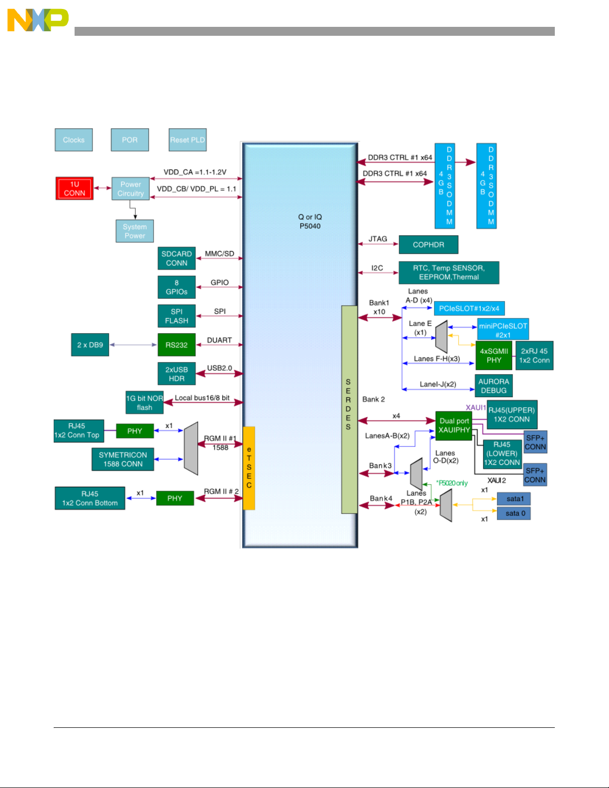
Block Diagram
3 Block Diagram
This figure depicts the general features and connectivity of the P5040/P5020 reference board.
Figure 1. P5040/P5020 Reference Board Block Diagram
P5040/P5020 Reference Design Board User Guide, Rev. 0
4 Freescale Semiconductor
Page 5
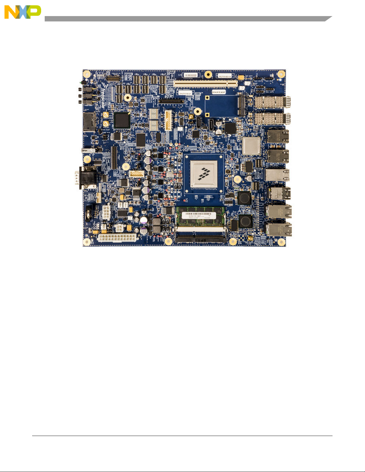
This figure shows the P5040 reference design board.
Evaluation Support
Figure 2. P5040 Reference Design Board
4 Evaluation Support
4.1 P5040/P5020RDB as a Processor Reference Board
For general hardware and/or software development and evaluation purposes, the P5040/P5020 reference
design board can be used like an ordinary, desktop computer.
The P5040/P5020 reference board can also be used as reference for many features of the P5040/P5020.
This table summarizes the processor hardware interfaces that can be evaluated by using the reference
board.
NOTE
Shaded features apply to only one processor.
P5040/P5020 Reference Design Board User Guide, Rev. 0
Freescale Semiconductor 5
Page 6
Evaluation Support
Table 2. P5040/P5020RDB device Interfaces
Device Feature Configuration Options
SerDes • Connect to PCI Express 2.0 x1 and x4 slots for use with graphics or other PEX cards
• Test via PCI Express card (typically graphics) or Catalyst™ PCI Express control/monitoring card
DDR3 • Memory controller capable of supporting DDR3 and DDR3-LV devices.
• Provides 2 SODIMM slots with one DDR3 8GB 204-pin 1.35/1.5v SODIMM module at 1333/1600 Mbps
data rate at 72-bit, and ECC support.
eSDHC SDMedia card and MMC card
SPI Supports standard 128Kbyte(2 MHz, 1.8V) and 16MB (100 MHz)
Local bus • Connects 8bit data and 10bit address to system control FPGA to access programming model to configure
system: Internal debug
Serial UART supports two 4-wire serial ports
I2CI
2
C bus #1 can be used for the following:
• Boot initialization code
• System EEPROM (MAC address storage, serial number, and so on)
• Fiber optic mode for XAUI ports 1 and 2
2
C bus #2 can be used for the following:
I
• DDR SODIMM SPD
2
C bus #4 can be used for the following:
I
• System RTC clock and CPU Thermal monitorl
Clocking • SerDes clock generator for XAUI PHY, SGMII PHY,and PCI Express slots
• RMII clock and buffers
GPIO Eight GPIOs are connected FPGA for future usage
IRQs EVENT switch normally asserts IRQ* but can drive SRESET0, and/or SRESET1 via software setting
Power 1U power supply to P5040/P5020 connector VCC_12, VCC_5_STBY, VCC_RTC_BAT
4.2 Reference Design Board Use
In the absence of a special hardware or software configuration, the P5040/P5020 reference design board
operates identically to a development/evaluation system.
4.3 Embedded Use
Section 6.1, “Configuration Options,” and Section 6.2, “Configuration Modes,” provide the FPGA and
external configuration switch settings used for start-up configuration information for U-Boot or Linux
when the system is used as an embedded platform.
4.4 Difficult-to-Find P5040/P5020 Connections
P5040/P5020 Reference Design Board User Guide, Rev. 0
6 Freescale Semiconductor
Page 7
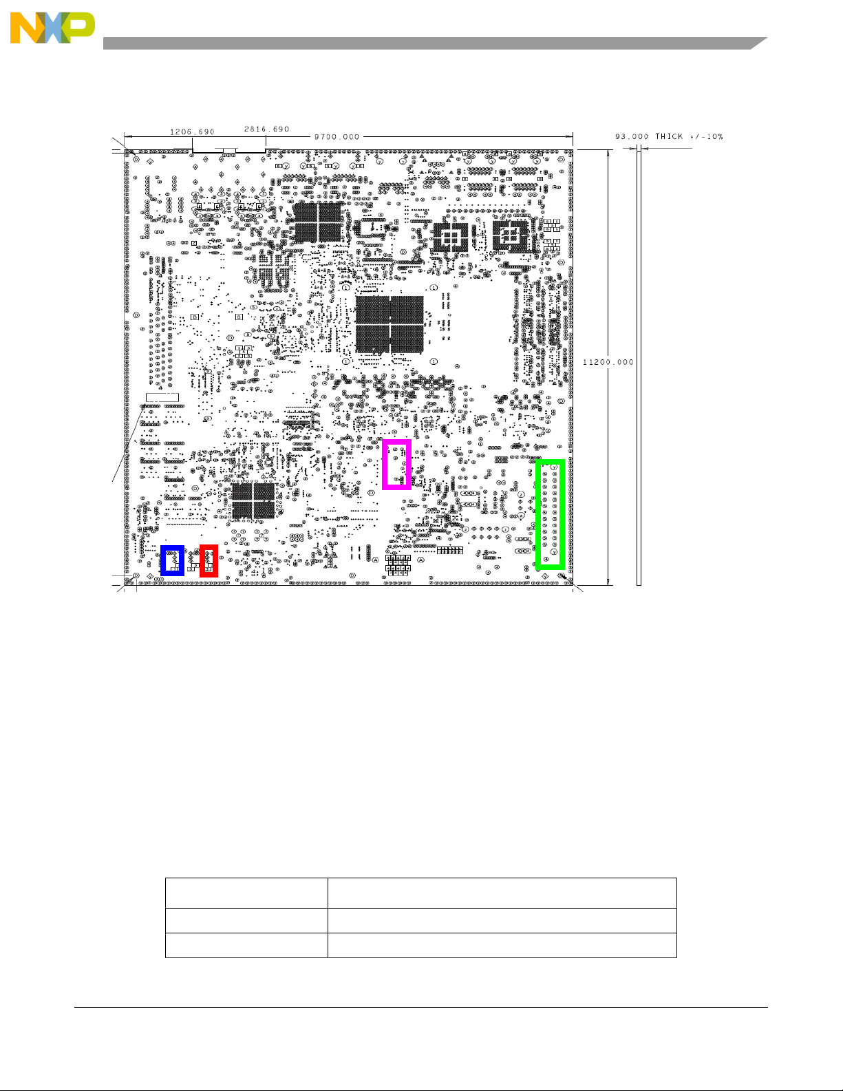
This figure shows connections that are difficult to find on the COM Express reference board.
Key:
1U power connector
SW3 power-on button
SW1 local reset
FPGA programming header
Architecture
Figure 3. Difficult-to-Find Connections—P5040/P5020 reference board Top View
5 Architecture
5.1 Processor
This table lists the major pin groupings of the P5040/P5020.
Table 3. P5040/P5020 Pin Groupings Summary
Signal Group Details
Memory Controllers Section 5.1.1, “DDR”
SerDes x18 Section 5.1.2, “SerDes x20/x18 Interface”
P5040/P5020 Reference Design Board User Guide, Rev. 0
Freescale Semiconductor 7
Page 8
Architecture
Table 3. P5040/P5020 Pin Groupings Summary (continued)
Signal Group Details
Ethernet Section 5.1.3, “Ethernet Controller (EC) Interfaces”
™
IEEE 1588 Section 5.1.4, “Support for IEEE Std 1588
Serial interfaces Section 5.1.5, “Serial Interfaces”
eSDHC Section 5.1.7, “enhanced Secure Digital Host Controller
(eSDHC) & embedded Multi Media Controller (eMMC)”
SPI Section 5.1.6, “enhanced Serial Peripheral Interface (eSPI)”
UART Serial Por ts Section 5.1.8, “UART Serial Ports”
USB Section 5.1.9, “USB Interfaces”
DMA Section 5.1.10, “DMA Controllers”
eOpenPIC Section 5.1.11, “eOpenPIC Interrupt Controller”
GPIO Section 5.1.12, “GPIO Signals”
System Control Section 5.1.13, “Control Group”
2
I2C Section 5.1.14, “I
C”
Protocol”
EM1 and EM2 Management Section 5.1.15, “EM1 and EM2 Management Buses”
Debug/Power Management Section 5.1.17, “Debug Features”
Clock Section 5.1.18, “Clock”
Thermal Section 5.1.19, “Temperature Anode and Cathode”
Power Section 5.1.20, “Power”
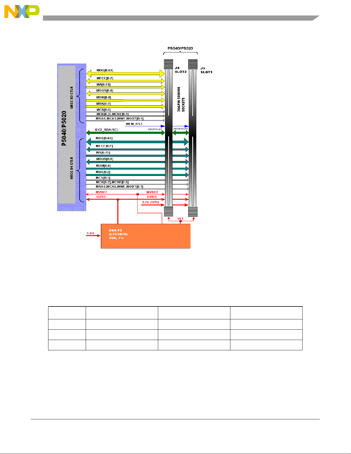
5.1.1 DDR
The P5040/P5020RDB contains a number of DDR-related features, as follows:
• Memory controller capable of supporting DDR3 and DDR3-LV devices
• Supports DDR3 using one 8GB, 1.35V/1.5V 204-pin Micron MT18KSF1G72HZ-1G6E2
SODIMM module @ 1333/1600 Mbps data rate at 72-bit, and ECC support
• Memory interface includes all necessary termination and IO power and is routed in order to achieve
maximum performance on the memory bus.
• As noted in the table below, P5040/P5020 has a dual DDR controller connected to dual DDR3
SODIMM slots.
Table 4. DDR Features
DDR Feature Description
DDR3 Topology Each controller connects to its own SODIMM slot.
Supports write-leveling intended to help determine timing skews.
Termination All input signal lines are terminated at the DIMM modules.
Additional termination is not required.
P5040/P5020 Reference Design Board User Guide, Rev. 0
8 Freescale Semiconductor
Page 9
Architecture
Figure 4. DDR interface
5.1.1.1 DDR Power
P5040/P5020RDB DDR power supplies these voltages.
Figure 5. DDR Power Supply
Voltage Name Voltage Current Note
GVDD 1.5V/1.35V > 10A DRAM core and IO
MVREF 0.75V/0.675V >= 10mA DRAM reference voltage
VTT 0.75V/0.675V >= 3A Bus termination supply
The P5040/P5020RDB uses the Linear Technology LTC3876 (U55) switching power controller as
follows:
• Dual-phase controller for up to 20 A at a default at 1.35 v adjustable to 1.5 V output.
• Supplies GVDD, VREF , and VTT for SODIMM DRAM DDR3 and P5040/P5020 DDR controller .
P5040/P5020 Reference Design Board User Guide, Rev. 0
Freescale Semiconductor 9
Page 10

Architecture
The following summarizes the use of MECC pins on the P5040/P5020RDB:
• RDB does not directly support MECC pin usage to access internal debug information. Since the
RDB does not provide a dedicated MUX, it has simpler routing and signal integrity status.
• However, as the RDB does not interfere with the controller-to-DDR path, access to debug
information on MECC pins is possible by using a NextWave (or equivalent) DDR logic analyzer
connector and non-ECC DDR modules.
5.1.2 SerDes x20/x18 Interface
The SerDes block on the P5040/P5020 provides high-speed serial communications interfaces for several
internal devices. The SerDes block provides 20 or 18 serial lanes for the P5040 or P5020, respectively.
They may be partitioned as shown in Table 5(a) or (b), respectively.
Note that the term ‘lane’ is used to describe the minimum number of signals needed to create a
bidirectional communications channel; in the case of PCI-Express or Serial RapidIO, a lane consists of two
differential pairs, one for receive and one for transmit, or four in all.
Table 5, top down, shows the following clocking banks and how they are configured by the reference
board:
Bank1 Lanes A–D go to x4 slot 1, E is demuxed to either x1 slot 2 or combined with lanes
E-F to support 4 SGMII ports, and I–J to the Aurora debug connector
Bank2 Lanes A–D go to port 1 of dual-ported XAUI PHY
Bank3 Lanes A–B of P5040 goes to port 2 of dual-ported XAUI PHY while lanes C and
D of P5020 could be demuxed to either go to SATA ports 1 and 2 or go to port 2
of dual-ported XAUI PHY.
Bank 4 Lanes P1B and P2A of P5040 are muxed are with lanes C–D of P5020 to SATA
ports 1 and 2.
Table 5. P5040/P5020 SerDes Lane Multiplexing Configurations on P5040/P5020
Bank 1 Bank 2 Bank 3
ABCD E F G H I J A B C D A B C D
0 1 2 3 4 5 6 7 8 9 10 11 12 13 14 15 16 17 — —
SLOT 1 SLOT 2
PCIe1
(5/2.5G)
PCIe1
(5/2.5G)
PCIe2
(5/2.5G)
SGMII
FM2
SGMII
FM2
SGMII
FM2
SGMII
FM2
Aurora Conn on
P5040 (RCW 02 and 34)
Debug (5/2.5G) XAUI FM1 XAUI FM2
Debug (5/2.5G) XAUI FM2 ——SATA1SATA2——
SLOT 3
SATA
Port1
SATA
Port2
————
Bank
4
P1B
SATA1
P2A
SATA2
P5020 (RCW 34 and 35)
P5040/P5020 Reference Design Board User Guide, Rev. 0
10 Freescale Semiconductor
Page 11

Architecture
Table 5. P5040/P5020 SerDes Lane Multiplexing Configurations on P5040/P5020 (continued)
Bank 1 Bank 2 Bank 3
ABCD E F G H I J A B C D A B C D
Bank
4
P1B
0 1 2 3 4 5 6 7 8 9 10 11 12 13 14 15 16 17 — —
SLOT 1 SLOT 2
PCIe1
(5/2.5G)
PCIe1
(5/2.5G)
PCIe2
(5/2.5G)
SGMII
FM2
SGMII
FM2
SGMII
Aurora Conn on
SLOT 3
——Debug (5/2.5G) XAUI FM1 — —
FM2
SGMII
FM2
Debug (5/2.5G) XAUI FM1 ——
SATA
Port1
SATA
Port2
————
——
SATA1
SATA2
——
SATA1
SATA2
P2A
P5040/P5020 Reference Design Board User Guide, Rev. 0
Freescale Semiconductor 11
Page 12
Architecture
P5040/P5020
SD_TX/RX[0:3](p,n)
PEX Slot 1
TX/RX[0:3](p,n)
REFCLK_SD1(p,n)
100 MHz
PEX Slot 2
TX/RX[4:7](p,n)
Aurora Conn
TX/RX[1:0](p,n)
SD_TX/RX[4:7](p,n)
SD_TX/RX[8:9](p,n)
x4 PCIe Card
Aurora Debug
x1 PCIe card
x4 SGMII PHY
Connector
Figure 6. P5040/P5020 SerDes Bank1 to Reference Board Cards/
Debug Connector Configuration
12 Freescale Semiconductor
P5040/P5020 Reference Design Board User Guide, Rev. 0
Page 13
Architecture
P5040/P5020
REFCLK_SD2/3/4(p,n)
125 MHz
Port 1 of TN8022
TX/RX[0:3](p,n)
SATA port1 & 2
TX/RX[1:2](p,n)
SD_TX/RX[10:13](p,n)
SD_TX/RX[14:17](p,n)
SATA connectors
2 COPPER PORTS
Port 2 of TN8022
p5040B3lanesA-D
p5020B3lanesCD
2 SFP+ PORTS
SD_TX/RX[P1B,P1A](p,n)
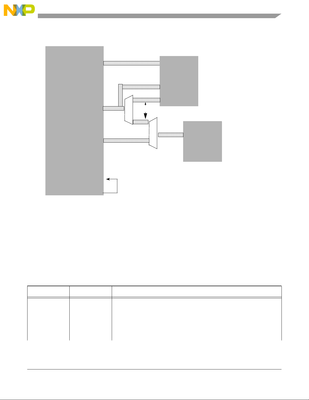
5.1.3 Ethernet Controller (EC) Interfaces
The two TSEC—with twisted pair 10/100/1000-Base-T interface—are IEEE 802.3-compliant. Vitesse
VSC8244 PHY supports four integrated PHYs though only two are in use. The P5040/P5020RDB only
uses the RGMII protocol.
This table shows the general organization of the ETH system.
GETH Feature Specifics Description
GETH Clocks IDT
Figure 7. P5040/P5020 SerDes Banks 2,3, and 4 to Reference Board XAUI ports/
SATA Connectors Configuration
ICS8304AMLF
Table 6. 10/100/1000 Base-T GETH Ports
• Low skew Fanout Buffer
• Receives 125MHz clock oscillator input and generates four LVCMOS/LVTLL
outputs:
– P5040/P5020 EC1_GTXCLK_125 clock input
– P5040/P5020 EC2_GTXCLK_125 clock input
– P5040/P5020 1588 clock input
– VSC8244 PHY XTAL1 input
Freescale Semiconductor 13
P5040/P5020 Reference Design Board User Guide, Rev. 0
Page 14

Architecture
Table 6. 10/100/1000 Base-T GETH Ports (continued)
GETH Feature Specifics Description
GETH
Copper Interface • Integrated GETH RJ45 Connector for EC1 and USB TypeA connector for USB1
Connectors
PHY
CMODE[7...0] Inputs used to configure VSC8244 hardware operating modes by connecting
Configuration
PHY Default
Configuration
PHY Control MII Management
Por t
MAX4906 Analog switch that chooses EMI1 routing.
EMI1 • Routing determined by one of the following:
PHY Reset VSC8244
PHY RESET
VSC8244
SOFT_RESET
(J2)
0
RJ45 connector for EC2 (P1)
•90
Pull-up/down resistors.
• MAC interface select: RGMII to CAT5.
• Speed/Duplex auto negotiation: 10/100/1000 Base-T HDX, FDX.
• PHY address[4:2] = ’000’
• Controls the following via the two-wire interface port:
– EMI1_MDC clock
– EMI1_MDIO bi-directional data line
– P5040/P5020 GPIO[0...3]
– ngPIXIS registers PX_BRDCFG1 and PX_BRDCFG2
• Input is driven by the P5040/P5020 HRESET
signal via FPGA, and reset after
each P5040/P5020 HRESET sequence.
• Input can be driven by register PX_RST P5040/P5020RDB FPGA Bit 7.
• Input is driven by the P5040/P5020 HRESET
each P5040/P5020 HRESET
sequence.
signal via FPGA, and reset after
• Input can be driven by register PX_RST P5040/P5020RDB FPGA Bit 5.
• Can implement by asserting bit 15 (MSB) on VSC8244 PHY MII Mode Control
Register 0.
P5040/P5020 Reference Design Board User Guide, Rev. 0
14 Freescale Semiconductor
Page 15
Architecture
MI
CLKBUF
EC #2
EC #1
ENET PHY
1
2
GTXCLK
EC Port #1
USB Port #1
125 MHz
To USB1
EC Port #2
To 1588 Riser Card Connector
P5040/P5020
Figure 8. P5040/P5020 Ethernet Connections to the Reference Board
This table summarizes the reference board EC connections and routing when the board is populated with
a P5040 or P5020 processor.
Table 7. P5040/P5020 Ethernet Port Locations on P5040/P5020
P5040/
P5020 EC #
1 1 0 Conn. J6 top
2 2 1 Conn. P1
Connection Port PHY Address Location
See Section 5.1.9, “USB Interfaces.”
P5040/P5020 Reference Design Board User Guide, Rev. 0
Freescale Semiconductor 15
Page 16
Architecture
TX >
P5040/P5020
STMP_TX/RX[1:2]
CLKIN
XTALOSC
125.000 MHz
±25 ppm
1588
CLKOUT
TRIGIN[1:2]
ALARMOUT[1:2]
Symmetricon
Riser Connector
PULSEOUT[1:2]
5.1.4 Support for IEEE Std 1588™ Protocol
The reference board supports the P5040/P5020 IEEE® 1588 precision time protocol (PTP) as shown in
Figure 9. This facility works in tandem with an Ethernet controller to timestamp incoming packets.
Figure 9. IEEE® 1588 Interface to Reference Board Symmetricon Riser Connector
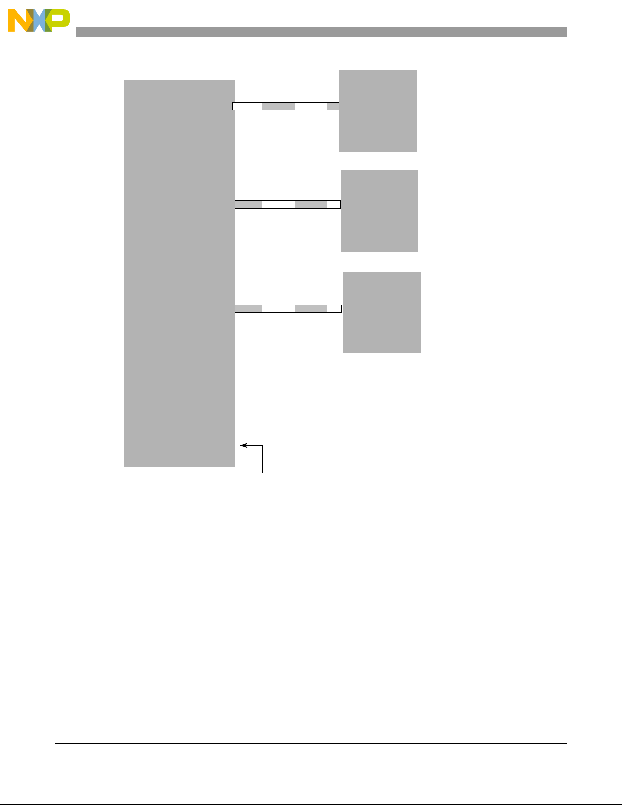
5.1.5 Serial Interfaces
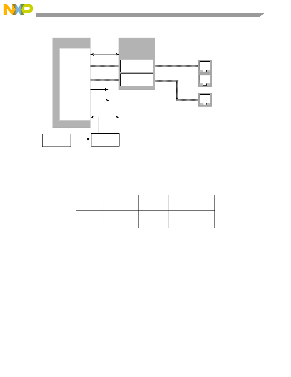
This figure shows overall connections of RS-232, eSPI, and eSDHC/eMMC interfaces.
16 Freescale Semiconductor
P5040/P5020 Reference Design Board User Guide, Rev. 0
Page 17
Architecture
Figure 10. Serial Interfaces
5.1.6 enhanced Serial Peripheral Interface (eSPI)
The P5040/P5020 has an eSPI Master Controller used to communicate with various peripherals.
• Two SPI FLASH support 24-bit address and SPI Modes 0, 3.
• Use Chip Select 0 or 1 with S25FL129P0XNFI001 FLASH if CVDD=3.3 V.
• Use Chip Select 2 with 25AA1024T-I/SM FLASH for all CVDD voltages (1.8, 2.5, or 3.3 V).
• Chip Select 3 is reserved for 1588 Riser Card.
This table describes the P5040/P5020RDB SPI FLASH memory.
P5040/P5020 Reference Design Board User Guide, Rev. 0
Freescale Semiconductor 17
Page 18

Architecture
Table 8. eSPI Slave devices
Device
Spansion
S25FL129P0XNFI001
Microchip
25AA1024T-I/SM
1588 Riser Card — 1.8–3.3 — CS3
Clock Frequency
(MHz)
104 2.7–3.3 16 MB CS[0,1]
2, 10, 20 1.8–3.3 128 KB CS2
Voltage Range (V) Capacity SPI CS
5.1.7 enhanced Secure Digital Host Controller (eSDHC) & embedded Multi Media Controller (eMMC)
The P5040/P5020 processor has an eSDHC and an eMMC controller, which the P5040/P5020 connects to
an SD media card slot. The I2C3_SDA signal uses write protect (WP). The I2C3_SCL signal uses card
detect (CD). The DS supports the following:
• 1.8, 2.5, and 3.3V SD/eMMC media card voltages.
• x4-bit and x8-bit cards though the latter uses SPI_CS[0:3] signals as eSDHC_DAT[4:7].
— eSDHC_DAT[4:7] signals are shared with SPI CS pins.
— Software can route the pins to either eSDHC/eMMC cards or SPI devices; however, they
cannot be used simultaneously.
CAUTION
Insert an SD/eMMC media card suited to P5040/P5020 CVDD voltage.
5.1.8 UART Serial Ports
Two RS-232 transceivers on the P5040/P5020RDB contribute to user application development and
provide convenient communication channels to both terminal and host computers. The transceivers are
connected to P5040/P5020 dedicated UAR T ports: one provides interconnection to DUT UART1/3 ports
or ngPIXIS FPGA; the other explores UART2/4 dedicated ports.
Analog Devices’ ADM561JRSZ product internally generates required RS-232 levels from 3.3V_HOT
supply.
NOTE
Powering from the 3.3V_HOT power rail is possible even when
P5040/P5020 is powered down. Thus, the FPGA processor can run
programs and interact with the user while allowing board reconfiguration
while sealed in the chassis.
This table describes the P5040/P5020RDB RS-232 interface.
P5040/P5020 Reference Design Board User Guide, Rev. 0
18 Freescale Semiconductor
Page 19

Architecture
Table 9. P5040/P5020RDB RS232 Interface
UART Ports Destination Power supply Flow control External Connector
UART1 Terminal (Host
UART3 Unsupported
UART2 Supported UART2/4 (J5 Top)
UART4 Unsupported
Computer)
3.3V_HOT Supported UART1/3 (J5 Bottom)
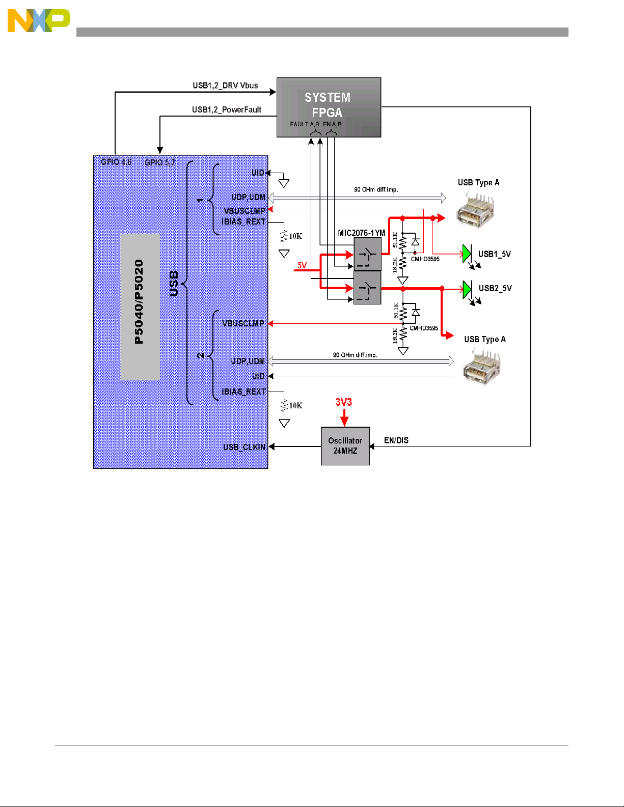
5.1.9 USB Interfaces
The P5040/P5020 has dual HS USB transceivers whose main features are as follows:
• Compliance with USB Specification, USB Rev. 2.0.
• USB 2.0 Transceiver Macrocell Interface (UTMI) with Link Controller.
• Supports HS, FS, and LS modes of operation.
• Supports signalling.
• Supports Host and Device modes.
— Working in Host mode only, the RDB connects a USB transceiver to connector Type A thus
enabling communication with keyboards, mice, memory sticks, etc.
— Working in Host and Device modes, a second USB transceiver connects to a second Type A
connector which has bus signal connecting directly to the P5040/P5020 internal PHY.
The 24MHz USB block reference clock provides additional control to the P5040/P5020 in conjunction
with the USB power sequence. GPIO 4,6 control the VBUS Drive. GPIO 5,7 get Power Fault indications
via the FPGA.
This figure shows the P5040/P5020RDB USB interface.
P5040/P5020 Reference Design Board User Guide, Rev. 0
Freescale Semiconductor 19
Page 20
Architecture
Figure 11. P5040/P5020 USB Connection to Reference Board USB Interfaces
5.1.10 DMA Controllers
The P5040/P5020 DMA controllers have internal and external controls to initiate and monitor DMA
activity. The reference board does not incorporate any specific devices that make use of the external
pin-controlled DMA controllers.
The P5040/P5020 DMA ports are connected to test points on the reference board to allow external
hardware control, as needed.
P5040/P5020 Reference Design Board User Guide, Rev. 0
20 Freescale Semiconductor
Page 21
Architecture
5.1.11 eOpenPIC Interrupt Controller
The reference board contains numerous interrupt connections. The P5040/P5020 eOpenPIC connections
to the P5040/P5020 are shown in this table.
Table 10. P5040/P5020 Interrupt Assignments
Signal Name Interrupt Source Description
IRQ0_B — —
IRQ1_B DS3232 (U50) System RTC.
IRQ2_B Zilker ZL6100 PS_CB Two ZL6100 SALRT outputs.
Zilker ZL6100 PS_GVDD
IRQ3_B Onboard RGMII PHY (J36) • VSC8244 interrupts 0,1 (wire-OR’d)
• Optional 1588 Riser Card
IRQ4_B ngPIXIS FPGA From Local Event Switch.
IRQ5_B NOR FLASH Memory RD/BY
IRQ6_B Reserved
IRQ7_B
IRQ8_B
IRQ9_B
IRQ10_B Analog Device Thermal Monitor ADT461 ALERT PIN
IRQ11_B THERM PIN
IRQ_OUT_B P5040/P5020 ngPIXIS FPGA used as an EVT pin.
Indicates completion of FLASH programming.
5.1.12 GPIO Signals
FPGA provides the control for EMI1 mux; therefore, software can configure the MDIO bus. See the MDIO
section for how to select between RGMII and SGMII PHY.
Table 11. Future Options for Configuring P5040/P5020-Dedicated GPIO Signals
for EMI MDIO Bus Multiplexing
Signal Name System Function
GPIO[0:1] EM1 management bus mux control
GPIO[4:7] Spares connected to test points
5.1.13 Control Group
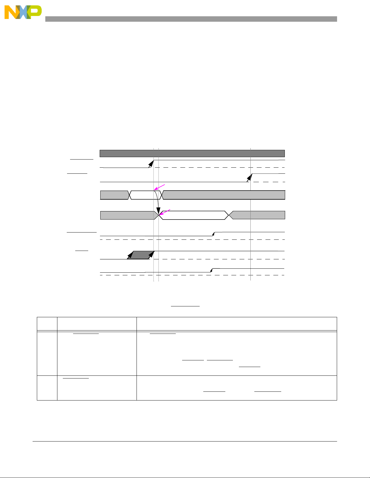
P5040/P5020 control group signals, for the most part, stop or restart execution. Figure 12 gives a
connections overview and shows the POR flow while Table 12 outlines the POR sequence.
• Legacy COP and Aurora connector resets are muxed to the ngPIXIS FPGA.
P5040/P5020 Reference Design Board User Guide, Rev. 0
Freescale Semiconductor 21
Page 22
Architecture
Stable CLKIN
PORESET
Min 32 CLKIN cycles
HRESET(IO)
PLLs are locked
(output)
RESET_REQ
Device ready, can start Pre-Boot
(output)
TRST
(Input)
(Input)
(Output)
(Reset Configuration Word-512 bit)
Start Load Reset Configuration
CFG Signals
Sampling point, when PORESET is negated
ASLEEP
(Reset Configuration Input Signals)
RCW
High Impedance
High Impedance
• ngPIXIS FPGA injects system-level resets along with legacy COP or Aurora resets.
• Legacy COP HRST is mapped to the P5040/P5020 POR.
• Legacy COP SRST is mapped to the P5040/P5020 HRESET.
• P5040/P5020 HRST is a bi-directional open drain signal; it is not monitored by ngPIXIS FPGA.
NOTE
Reset configuration input signals are ONLY sampled at the negation of
POR. Reset Configuration input pins—CFG_RCW_SRC[4...0],
CFG_SVR[1...0], CFG_GPINPUT[15...0], CFG_ENG_USE[3...0],
CFG_ELBC_ECC, CFG_DRAM_TYPE—function differently when a
device is not in a reset state.
Step Sequence Stage Description
1 PORESET
2 PORESET
22 Freescale Semiconductor
Figure 12. Power-on Reset Sequence
Sequence
/ PORESET to load a new RCW to the device.
throughout PORESET.
.
Table 12. PORESET
: General
Information
: During Negation 1. Sampling of input signals determines the interface to be loaded into the
P5040/P5020 Reference Design Board User Guide, Rev. 0
1. PORESET is asserted.
2. FPGA drives CFG_RCW_SRC[4...0] and all reset configuration input signals
to P5040/P5020; see Ta bl e 1 3.
3. P5040/P5020 loads RCWs.
4. FPGA drives HRESET
P5040/P5020 loads the RCW during HRESET
device.
2. P5040/P5020 asserts HRESET
Page 23

Architecture
Table 12. PORESET Sequence
Step Sequence Stage Description
3 PORESET: After Negation 1. P5040/P5020 begins the configuration process and starts loading reset
configuration.
2. Host debugger controls PORESET
configuration).
4 Configuration Input Reset configuration inputs are sampled to determine the following:
• Configuration source: CFG_RCW_SRC[4...0]
• CFG_DBG_RST_DIS
• CFG_ENG_USE[3...0]
• CFG_PLL_CONFIG_SEL_B
• CFG_POR_AINIT
• CFG_RCW_SRC_SLEW
• CFG_TEST_PORT_DIS
• CFG_TEST_PORT_MUX_SEL
• CFG_XVDD_SEL
• DRAM Type Select (DDR3 or DDR3L): CFG_DRAM_TYPE
• General Purpose Input: CFG_GPINPUT[15...0]. Only two[1...0] are driven.
• NAND FLASH ECC Enable: CFG_ELBC_ECC
• Response Disable: CFG_RSP_DIS
• System Version Register: CFG_SVR[1...0]
processor signal (which sets a chosen
5 Configuration Time Time required varies according to configuration source and CLKIN frequency.
NOTE
The P5040/P5020RDB has default DIP-switch settings that can be manually
repositioned as per user selected configuration levels. Several RCW bits
only can be changed by DIP-switches.
P5040/P5020 Reference Design Board User Guide, Rev. 0
Freescale Semiconductor 23
Page 24

Architecture
This table lists RCW sources.
Table 13. Reset Configuration Word Source
Value (Binary) Reset Configuration Signal Name Description
0_0000 CFG_RCW_SRC[4...0] I
0_0001 I
0_0010 Reserved
0_0011 Reserved
0_0100 SPI 16-bit addressing
0_0101 SPI 24-bit addressing
0_0110 eSDHC
0_0111 Reserved
0_1000 eLBC FCM (NAND FLASH, 8-bit small page)
0_1001 eLBC FCM (NAND FLASH, 8-bit large page)
0_1010 Reserved
0_1011 Reserved
0_1100 eLBC GPCM (NOR FLASH, 8-bit)
0_1101 eLBC GPCM (NOR FLASH, 16-bit)
0_1110 Reserved
0_1111 Reserved
2
C1 normal addressing supports ROMs up to 256 bytes.
2
C1 extended addressing
1_0000 -1_1011 Hard-coded RCW options
1_1100-1_1111 Reserved
5.1.14 I2C
The reference design board uses three of the four I2C buses on the P5040/P5020.
•I2C1 is electrically isolated before P5040/P5020 power-up to allow external or FPGA I2C masters
to program Zilker power devices.
2
•I
C2 and I2C4 can function independently, or together with I2C2 as the controller.
This table summarizes I2C bus device addresses while Figure 13 shows overall I2C scheme connections.
Table 14. I2C Bus Device Map
I2C Bus I2C Address Device Notes
1 0x22 LTC3889: VCORE PM Bus (TBD) Controls rail VDD_CORE.
1 0x24 LTC3876 regulator: DDR PM Bus (TBD) Controls rail VDD_GVDD.
P5040/P5020 Reference Design Board User Guide, Rev. 0
24 Freescale Semiconductor
1
Page 25

Table 14. I2C Bus Device Map1 (continued)
I2C Bus I2C Address Device Notes
Architecture
1 0x27 Platform regulator LTC3880 (TBD)
Controls VDD_PL
I2C/SMBus Expander
1 0x50 Atmel AT24C64A or equivalent: 8192 bytes
EEPROM
1 0x55 Atmel AT24C02B or equivalent: 256 bytes
EEPROM
Stores RCW and PBLOADER data.
WP
Stores ngPIXIS accessed configuration
data.
Accessible when board is powered-off.
WP
1 0x56 Atmel AT24C64A or equivalent: 8192 bytes
EEPROM
Stores ngPIXIS GMSA program code.
Accessible when board is powered-off.
WP
1 0x57 Atmel AT24C02B or equivalent: 256 bytes
SYSTEM ID EEPROM
Stores board specific data, including
MAC addresses, serial number, errata,
etc.
WP
1 n/a ngPIXIS I
2
C Port For bus reset, monitoring, and
master-only data collection.
1n/aI
2
C Access Header For remote programming of boot
sequencer startup code (if needed) or
Zilker Lab PM Bus programmer.
2 0x51 DDR3 SODIMM Socket 1 SPD EEPROM
Type of device depends on uDIMM
vendor.
2 0x52 DDR3 SODIMM Socket 2 SPD EEPROM
Type of device depends on uDIMM
vendor.
2
2n/aI
C Access Header For remote programming of boot
sequencer startup code (if needed).
3 n/a Not used for I
2
C functionality. Used for alternate SD/eMMC functions:
SD_WP and SD_CD instead of I2C.
4 0x40 INA220 Current/Power Monitor(n/a) For current/power measurements on
P5040/P5020 GVDD.
4 0x41 INA220 Current/Power Monitor(n/a) For current/power measurements on
P5040/P5020 VDD_PL.
4 0x44 INA220 Current/Power Monitor(n/a) For current/power measurements on
P5040/P5020 VDD_CA.
4 0x45 INA220 Current/Power Monitor For current/power measurements on
P5040/P5020 VDD_CB.
4 0x4C ADT7461A or equivalent: Processor
Thermal Monitor
For measuring P5040/P5020
temperature.
4 0x68 DS3232: RTC Used by software.
P5040/P5020 Reference Design Board User Guide, Rev. 0
Freescale Semiconductor 25
Page 26

Architecture
Table 14. I2C Bus Device Map1 (continued)
I2C Bus I2C Address Device Notes
4n/aI
4 n/a ngPIXIS I
2
C Access Header For remote programming (if needed).
2
C Port For bus reset, monitoring, and
master-only data collection.
1
Map addresses do not include the position of a transmitted address LSB (R/W bit).
Figure 13. I2C Scheme
P5040/P5020 Reference Design Board User Guide, Rev. 0
26 Freescale Semiconductor
Page 27

Architecture
See Section 7, “Programming Model,” for I2C implementation information.
5.1.15 EM1 and EM2 Management Buses
The P5040/P5020 has the following types of buses:
• SGMII and RGMII PHY management
• XAUI PHY management
Because one set of buses must span across multiple devices on the reference board, multiplexers are used
to route from the P5040/P5020 to each SGMII and RGMII PHYs while EMI2_MDIO bus is routed to
XAUI PHY. See Section 7, “Programming Model,” for details on using GPIO to select EMI1 device.
PHY management bus control is summarized in this table.
Table 15. P5040/P5020 PHY Management Bus Map for EMI1 on Reference Board
Bus FPGA_S1S0 Device
EMI1 00 On board RGMI PHYI
EMI1 01 SGMII
5.1.16 Enhanced Local Bus (eLBC) Interface
The eLBC has the following features:
• Supports GPCM, NAND FCM, and UPM.
• Only operates in 3.3V IO voltage.
• Clients include: PromJet Emulator, FPGA, NOR and NAND FLASH.
P5040/P5020 Reference Design Board User Guide, Rev. 0
Freescale Semiconductor 27
Page 28

Architecture
This figure shows the eLBC block diagram.
Figure 14. eLBC Interface
P5040/P5020 Reference Design Board User Guide, Rev. 0
28 Freescale Semiconductor
Page 29

This table summarizes local bus chip select routing.
Table 16. Local Bus Chip select Mapping
Architecture
FLASH Selection
cfg_lbmap
1010–1111 Invalid
1
cfg_lbmap[0:3] are user configuration DIP-switches.
1
[0:3]
0000 LCS0 LCS[2,4:6] LCS1 LCS3 Boot from NOR FLASH region #0
0001 Boot from NOR FLASH region #1
0010 Boot from NOR FLASH region #2
0011 Boot from NOR FLASH region #3
0100 Boot from NOR FLASH region #4
0101 Boot from NOR FLASH region #5
0110 Boot from NOR FLASH region #6
0111 Boot from NOR FLASH region #7
1000 LCS1 LCS[2,4:6] LCS0 — Boot from PromJet & NOR FLASH unbanked.
1001 LCS2 LCS[0,4:6] LCS1 — Boot from NAND & NOR FLASH unbanked.
NOR
FLASH
NAND
FLASH
PromJet ngPIXIS Description
5.1.16.1 Address Latch/Data Transceivers
TI device SN74ALVTH32373ZKER provides address latch while the On Semiconductor device
MC74LCX16245DTG provides dual data transceivers.
A transceiver latch enable (LE) input signal is driven by a P5040/P3041/P5020 LALE output signal.
• When LE is taken low, transceiver Q outputs are latched at input-set levels.
• Latched LA[0:26] + LA[27:31] comes directly from the CPU to build a full LA[0:31] address bus.
• The data bus was built with data buffers controlled by the CPU_LBCTL signal.
• D[0:26] is muxed with address.
• D[27:31] is only defined as data.
5.1.16.2 NOR FLASH
Spansion in-socket NOR FLASH memory (S29GL01GP11TFIR1) has 128 MB and a 16-bit data width.
The FLASH is controlled by the GPCM local bus. Bus data is obtained from the data transceiver. For
address information, see Section 5.1.16.1, “Address Latch/Data Transceivers.”
FLASH functioning is as follows:
• Local bus LOE
•FLASH RY/BY output signal detects the completion of FLASH programming or erasure. The
signal is connected to the P5040/P5020 IRQ5
controls FLASH OE while LWE0 controls the FLASH WE signal.
interrupt line.
P5040/P5020 Reference Design Board User Guide, Rev. 0
Freescale Semiconductor 29
Page 30

Architecture
•CS0, CS1, or CS2 select NOR FLASH depending on “CFG_Vbank[0...2]”.
• FPGA-generated signals are used to re-arrange internal addresses as per user configuration options
“CFG_LBMAP[0...3]”.
5.1.16.3 NAND FLASH
Micron NAND FLASH memory (MT29F4G08ABADAWP:D) has 512 MB and an 8-bit data width.
NAND FLASH is controlled by the FCM Local Bus.
• FLASH R/B output indicates the status of a device operation. This open drain output connects to
the P5040/P5020 LFR/B/LGPL4 line.
•CS0, CS2, or CS[4:6] select NAND FLASH as per “CFG_LBMAP[0...3]”.
5.1.16.4 PromJet Connector
A PromJet connector can be used for debugging purposes.
connected to the PromJet superset connector. The 16-bit PromJet modules (FLASH memory emulators)
are available from Emutec. See www.emutec.com.
CS0 or CS1 select between PromJet FLASH and onboard FLASH as per “CFG_LBMAP[0...3]”.
Perpiherals and embedded storage can be
5.1.17 Debug Features
The reference board provides a JT AG COP header and AURORA test points for debug purposes, using the
CodeWarrior USBTAP already installed in the system.
To upgrade the U-Boot stored on the NOR FLASH, use the CodeWarrior USBTAP tool.
5.1.18 Clock
For a description of the clock architecture, see Section 5.4, “Clocks.”
5.1.19 Temperature Anode and Cathode
The P5040/P5020 has two pins, Temp_Anode and Temp_Cathode, connected to a thermal body diode on
the die that allow direct temperature measurement. The pins are connected to an ADT7461 thermal
monitor that allows direct die temperature readings with an accuracy of ±1 °C.
5.1.20 Power
For a description of the clock architecture, see Section 5.3, “System Power Connections.”
5.2 System Control Logic
The P5040/P5020RDB contains FPGA ngPIXIS that implements the following functions:
• Resets sequencing/timing as per COP/JTAG connections.
• Maps/re-maps P5040/P5020 local bus chip selects to FLASH, compact FLASH, and so on.
P5040/P5020 Reference Design Board User Guide, Rev. 0
30 Freescale Semiconductor
Page 31

Architecture
PSU_PWR_GOOD
RESET
LOCAL
BUS
CONFIG
DRIVE
RESET
REG
RESETS
COP IO
REGISTERS
LBUS
CPU
COP
CONFIG
CONFIG
RESET SW
SEQ
• Transfers switch settings to processor/board configuration signals.
• Loads configuration data from RAM (registers) or EEPROM to override configuration (for
self-test).
• Miscellaneous system logic:
— COP reset merging
—I2C timeout reset
The FPGA is powered from standby power supplies and an independent clock. This allows the FPGA to
control all aspects of board bring-up, including power, clocking, and reset.
The ngPIXIS is implemented in an Actel A3P1000-FGG484 484-pad micro-BGA. This figure shows the
overall ngPIXIS architecture.
Figure 15. FPGA Overview
Main ngPIXIS features include the following:
CONFIG Configuration Monitors and/or sets selected configuration signals.
COP JTAG COP Handles, in a transparent manner, the merging of COP header resets with onboard
LOCALBUS Local Bus Interface between processor and REGFILE.
REGISTERS Register Files Multi-ported register file containing status and configuration data.
Freescale Semiconductor 31
Feature Description
P5040/P5020 Reference Design Board User Guide, Rev. 0
Table 17. ngPIXIS Features
resets.
Page 32

Architecture
Table 17. ngPIXIS Features (continued)
Feature Description
REGRESETS Register Resets Drives resets from one of the following: sequencer, register-based software control,
or VELA.
RESETSEQ Reset Sequence Collects various reset/power-good signals and starts the global reset sequencer.
5.2.1 CONFIG
CONFIG monitors and/or sets selected configuration signals, per the following examples.
• CONFIG can, in some instances, map switch settings into direct configuration outputs.
• For SYSCLK, it maps a 3-position switch into a 16-bit register initialization pattern that is
subsequently used to initialize the clock generator.
5.2.2 COP JTAG
COP JTAG handles, in a transparent manner, the merging of COP header resets with onboard resets.
• It is critical that COP_ HRST input reset the entire system EXCEPT for the COP JT AG controller;
for example, TRST must not be asserted.
• If COP JTAG is not connected to P5040/P5020RDB, then it is critical that reset assert TRST.
The COP core manages these modal operations.
5.2.3 LOCALBUS
LOCALBUS is the interface between processor and REGFILE; asynchronous signaling is used since
access to the internal registers may be blocked.
5.2.4 REGISTERS
REGFILE is a dual-port register file that contains several types of registers.
NOTE
REGFILE must be able to accept (or arbitrate for) concurrent writes to the
same register. This, however, is not a statistically likely occurrence.
5.2.5 REGRESETS
REGRESETS copies sequencer reset signals and allows register-based software to individually assert reset
to the local bus, memory, and/or compact FLASH interfaces.
5.2.6 RESETSEQ
RESETSEQ collects various reset/power good signals and initiates the global reset sequencer.
P5040/P5020 Reference Design Board User Guide, Rev. 0
32 Freescale Semiconductor
Page 33

Architecture
NOTE
ASLEEP negation indicates the processor has exited reset. ASLEEP
assertion does not cause reset because, following HRST, the processor can
“sleep” for multiple reasons.
Drivers can be driven following power up. Normal operation and/or use of the VELA engine can lead to
tri-stated IOs. During power-off, all IO and output drivers must be tri-stated.
5.3 System Power Connections
The 12-V, 5-V, and 3.3-V power requirements for the reference board are met by the attached 1U-12V
compatible power supply unit (PSU) of the P5040/P5020RDB. The 5 V and 3.3 V are connected to
individual power planes in the P5040/P5020RDB PCB stackup. The 12-V power from the standard 1U
header is treated as separate from the 1U-12V power, which supplies a large amount of current and is
referred to as VCC_12V_BULK. Other supplies include VCC_5VSTBY and VCC_BAT.
Note that to support the FPGA standby operation, video cards, or other high-power-dissipation cards in the
PCI Express slot, the PSU should support the following minimum specifications:
• Minimum 450 W overall, 500 W recommended
• PCIE 12 V supports a minimum of 150 W
• Minimum 5-V, 2-A standby current
All other power sources are also derived from the 1U PSU. The figure below shows the principal system
power connections in relation to the FPGA control. For details about the processor power scheme
implemented by this system, see the Power device feature row in Table 2.
P5040/P5020 Reference Design Board User Guide, Rev. 0
Freescale Semiconductor 33
Page 34

Architecture
SPS
+3.3VHOT
FPGA
LDO
+1.8VHOT
1U PSU
+5 V
+3.3 V
+12 V
+5VSTB
+12V_BULK
PWRGD
PWRON
Batt.
+2.5 V
+1.8 V
+1.2 V
VSTANDBY
+3.3 V HOT
Select
LDO
LDO
LDO
+1.5VHOT
LDO
+1.1V/1.0V
SWREG
CORE/PL
Figure 16. Power connections in relation to the FPGA control
5.3.1 Power Supplies
An 1U power supply SPI4601UG (460 W) is provided in the system to support the P5040/P5020 devices,
the reference board and all its I/O cards. VCC_12, VCC_12V_BULK, VCC_5V_STBY, and
VCC_RTC_BAT are provided from the reference board. In addition, the P5040/P5020RDB PS provides
all the voltages necessary for correct operation x2 DDR3 SODIMMs, GETH, FPGA, and all onboard
peripherals.
This figure details the power supplies.
34 Freescale Semiconductor
P5040/P5020 Reference Design Board User Guide, Rev. 0
Page 35

Architecture
Figure 17. Power Supplies
5.3.1.1 PDN of Main Power Supplies
To reduce cost, a LTC3880 switcher regulator is used to supply both VDD_CA and VDD_CB (core voltage) up to 30A, 1% tolerance. The same chip is also used to supply VDD_PL(platform voltage).
5.3.1.2 PDN Options
Figure 18 shows various main power supplies combination used for different DUT types (depends on
PROC_SEL switches: SW7[6:7], SW15[5]) as well as a lot of other optional power combinations which
could be used for testing purposes. Power options supported are for P5040/P5021 and P5020/P5010 as
shown highlighted in pink in the table below.
P5040/P5020 Reference Design Board User Guide, Rev. 0
Freescale Semiconductor 35
Page 36

Architecture
Figure 18. P5040/P5020RDB PDN Options
5.3.1.3 DDR
DDR SDRAM GVDD, termination (M_VTT) and reference (M_VREF) voltages are automatically set at
the noted limits, depending on SW1[6] "DRAM TYPE" following power on:
SW1[6] = “1” (DDR3 regular)
• DDR3 default GVDD = 1.5V
• M_VTT = 0.75V
• M_VREF = 0.75V
P5040/P5020 Reference Design Board User Guide, Rev. 0
36 Freescale Semiconductor
Page 37

SW1/6 = “0” (DDR3L low power)
• DDR3L default GVDD = 1.35V
• M_VTT = 0.675V
• M_VREF = 0.675V
5.3.1.4 LVDD
GETH LVDD voltage is set to 2.5V.
5.3.1.5 CVDD
CVDD voltage has these characteristics:
• Powers SD and SPI interfaces.
• Used to define IO_VSEL P5020 configuration pins setting.
• CVDD selection of 1.8, 2.5, or 3.3V is made by correctly setting J11.
• IO_VSEL is done automatically in compliance with selected CVDD values.
5.3.1.6 XVDD
Architecture
XVDD voltage has these characteristics:
• Powers the SERDES block IO.
• Voltage value is set to 1.5 or 1.8V using SW3[5] or a corresponding FPGA control bit.
5.3.1.7 VDD_CORE
VDD_CB voltage has the following characteristics:
• Powers both cores A and B of P5040/P5020 Rev 1.0 and 2.0 devices.
• Set SW6[7] to “0” to turn off voltage. The voltage connected/disconnected from corresponding
power plane in conjunction with selected PDN options (see Table 18)
5.3.1.8 POVDD
• Possible to set to 0V, 1.0V, or 1.5V.
• SW3[8] controls ON/OFF status of POVDD onboard secondary PS.
• SW8[6] selects desired POVDD value.
• J21 connects POVDD power line to a selected voltage OR “shorts” it to the GND plane.
5.3.1.9 BVDD & OVDD
BVDD (eLBC block) and OVDD (general IO) voltages are set to 3.3V.
P5040/P5020 Reference Design Board User Guide, Rev. 0
Freescale Semiconductor 37
Page 38

Architecture
5.3.1.10 USB
USB voltages has the following characteristics:
• USB transceiver: USB_VDD_3P3 voltage is set to 3.3V.
• USB PLL: USB_VDD_1P0 voltage is set to 1.0V.
• External periphery device power: USB1_VBUS, USB2_VBUS voltage = 5V corresponds to
USB1_PWR_EN, USB2_PWR_EN signal; otherwise, [default] USB_VBUS = 0V.
5.3.1.11 VDD_LP
VDD_LP voltage has the following characteristics:
• VDD_LP = 1.0V.
• Low-power security monitor supply: VCC_HOT3V3 or onboard battery BT1 (which is
independent of the main PS) supply voltage to the VDD_LP via LDO regulator U21.
• When the main ATX PS is powered and connected to the RDB (VCC_HOT3V3 is present) then
voltage is supplied to the CPU. Alternatively, the battery can supply voltage if J9 is “shorted.”
• Auxiliary J10, VDD_LP_DET, provides low-power, tamper detect functionality.
This table lists all possible VDD_LP voltage options.
Table 18. VDD_LP Voltage Options
VDD_LP J10 J9 VCC_HOT3V3 Battery VDD_LP_TMP_DETECT
1.0V 1-2
2-3
1-2
2-3
0V X X Not existing Not existing X
X Existing X On
Off
Short X Existing On
Off
5.4 Clocks
The reference board clock signals are generated by the board in use. Table 19 lists the requirements of the
reference board clock signals when the reference board is populated with a P5040 or P5020 processor . This
board uses a custom IDT 6T49278BNLGI8 clock to meet the requirements listed in the table below.
P5040/P5020 Reference Design Board User Guide, Rev. 0
38 Freescale Semiconductor
Page 39

This figure shows the principal clock connections for the P5040/P5020.
Conversely, the reference board provides a battery to the RTC clock to keep time while the system is turned off.
This table summarizes P5040/P5020 clock distribution.
NOTE
DDR clocks are provided by the P5040/P5020.
Page 40

Architecture
Table 19. P5040/P5020 Clock Distribution
Clock Frequency Destination Device
SYSCLK 33–200 MHz SYSCLK IDT ICS307M-02:
•t
typ = 1ns
R
typ = 1ns
t
F
• Duty-cycle <= 60%
• Jitter type = ± 120 ps
• 25MHz input clock oscillator
RTC ~50KHz RTCCLK FPGA
SD_REF_CLK1 100.00 MHz
125.00 MHz
156.25 MHz
SD_REF_CLK2 100.00 MHz
125.00 MHz
156.25 MHz
SD_REF_CLK3 100.00 MHz
125.00 MHz
156.25 MHz
SD_REF_CLK4 100.00 MHz
125.00 MHz
156.25 MHz
GTX_CLK125 125 MHz P5040/P5020
USB_PHYCLK 24 MHz USB_CLOCK_In Clock oscillator
FPGA_CLK 33.33 MHz FPGA Clock Oscillator
SD2_REFCLK(p,n)
SLOT1 REFCLK(p,n)
SD2_REFCLK(p,n)
SLOT2 REFCLK(p,n)
AURORA DEBUG REFCLK(p,n)
SD3_REFCLK(p,n)
TN8022 XAUI PHY
P5040 SD4_REFCLK(p,n)
• EC1_GTX_CLK125
• EC2_GTX_CLK125
• 1588_CLK_IN
(MUX with 1588 Riser Card REFCLK)
Vitess VSC8244 XTAL1
• IDT 6T49278BNLGI8 generator
• RMS phase jitter type <= 3.04ps
• Ten selectable 100MHz, 125MHz,
156.25MHz and 312.5MHz clocks for
PCI Express, sRIO and GbE, HCSL
interface levels r
IDT ICS8304AMLN
• 1-to-4 Fanout Clock Buffer
• 125MHz input clock oscillator
• Maximum output skew = 45ps
5.4.1 SYSCLK
A significant amount of P5040/P5020 timing is derived from SYSCLK input. The P5040/P5020 reference
design board has the following features:
• SYSCLK pin is controlled by an IDT ICS307M-02 frequency synthesizer.
• IDT device, as part of the reset/power-up sequence, is serially configured by 24 data bits via
ngPIXIS.
• 24 data bits can be controlled to set the SYSCLK speed to fine increments; this is done using the
dynamic (re)configuration facilities of remote access ngPIXIS.
• To ease configuration, ngPIXIS pre-loads the 24-bit configuration pattern; this is done using one
of eight popular values and by sampling three switches located on the motherboard,
SW_SYSCLK[0...2].
P5040/P5020 Reference Design Board User Guide, Rev. 0
40 Freescale Semiconductor
Page 41

Architecture
This table summarizes switch-selectable clock generation possibilities. The calculations are based upon
25 MHz reference clock input. “Control Word” field values are characterized as follows:
• Data was sent to ICS307 upon startup or if commanded by the FPGA VELA controller.
• Values were calculated from ICS307 data sheet examples or using the IDT on-line calculator.
• Values were calculated for frequency accuracy versus lowest-jitter; the latter parameter was
chosen.
Table 20. SYSCLK Frequency Options
SYSCLK_SEL[0...2]
0 0 0 67 66.666 4.985 0x370801
0 0 1 83 83.333 4.012 0x330601
0 1 0 100 100.000 0 0x330801
0 1 1 125 125.000 0 0x310381
1 0 0 133 133.333 2.503 0x310401
1 0 1 150 150.000 0 0x310501
1 1 0 160 160.000 0 0x310C03
1 1 1 167 166.666 2 0x310601
Desired SYSCLK
(MHz)
Actual SYSCLK
(MHz)
Error
(ppm)
ICS307
Control Word
5.5 System Reset
Figure 19 shows P5040/P5020RDB reset connections from which the following can be inferred:
• ngPIXIS registers are reset by every reset input as well as GO.
— GO is a VELA-controller output that is, in turn, controlled by ngPIXIS registers.
• Most ngPIXIS registers are reset by either RRST or XRST.
— PX_AUX is the exception; it is ONLY reset by RRST and is unaffected by COP_HRST and
wdog_rst.
• If the watchdog timer expires then all internal settings are reset. This includes VELA-controlled
configurations.
• If the COP_HRST signal is asserted then all internal settings are reset.This includes
VELA-controlled configurations.
• Reset sequencer is triggered at GO, COP_HRESET, or RST.
— Sequencer asserts CPU_TRST when triggered by GO and RST.
— Sequencer does NOT assert CPU_TRST when triggered by COP_HRST.
• Reset sequencer controls CPU_HRST. The sequencer must be active in order for the COP_HRST
signal to pass through.
• Conversely, CPU_TRST is wire-OR’ed with the sequencer.
P5040/P5020 Reference Design Board User Guide, Rev. 0
Freescale Semiconductor 41
Page 42

Architecture
ngPIXIS
PWRGD(SYSRST)
P5040/P5020
RRST
+
+
COP_TRST
GO
RESET
SEQ
PHY_RST
MEM_RST
GEN_RST
COP_HRST
HOTRST
RESET_REQ
wdog_rst
GO
RST
PORST
rreq_rst
COP_HRST
CPU_PORESET
TRST
CPU_TRST
HOTRST
Lower_case = internal signal
Upper case = external signal
+ XRST
ngPIXIS
No polarity information is shown
REGS
COP_SRST
CPU_HRESET
open drain
— Thus, COP directly controls the CPU_TRST.
Figure 19. P5040/P5020RDB Reset Hierarchy
5.5.1 System Reset Performed by the FPGA Reset Sequencer
The reference board FPGA contains a reset sequencer that properly manages the orderly bring-up of the
system. Note that this is not the same as the power sequencer , which is similar , but not sp ecifically related
to reset.
After the system transitions to having fully-stable power supplies, the reset sequencer performs the
following:
1. Waits for all reset conditions to clear.
2. Configures and releases the processor from reset.
3. Idles waiting for further reset conditions to occur.
This table summarizes the reset conditions and actions of the FPGA.
Signal Type Description Action
HOT_RST_B External HOT power stable Restarts all FPGA internal state machines and registers
PWRGD External 1U power stable Causes full system reset unless the system is in S3 (power
42 Freescale Semiconductor
Table 21. Reset Conditions and Actions of the FPGA Reset Sequencer
down) state
P5040/P5020 Reference Design Board User Guide, Rev. 0
Page 43

Architecture
Table 21. Reset Conditions and Actions of the FPGA Reset Sequencer (continued)
Signal Type Description Action
SYS_HRST_B External COP tool reset request Upon power good, sys_rst_b is sent to P5040/P5020 and all
peripheral functional blocks
RESET_REQ_B External CPU requests reset Full reset
5.5.2 Reset Terms
All reset operations are conducted within various portions of the ngPIXIS. See Section 5.2.6,
“RESETSEQ,” for details. This table summarizes the reset terms.
Table 22. Reset Terms
Reset Term Description Notes
Input Terms
COP_HRST
COP_SRST
COP_TRST
HOT_RST
PWRGD
RESET_REQ
VELA “GO”
CFG_DRV*
CPU_HRESET
CPU_PORESET
CPU_TRST
GEN_RST
MEM_RST
Asserted under System Reset Controller, Legacy COP, or
Aurora control.
Asserted under System Reset Controller, Legacy COP, or
Aurora control.
Asserted under Legacy COP or Aurora control. Mapped to CPU_TRST.
Asserted low until VCC_HOT_3.3 is stable; thereafter it is
negated high.
Asserted low:
• until ATX power supply is stable
• while system reset is asserted; e.g., motherboard
switch or chassis cable switch.
Assertion by CPU(s) begins self-reset. Short duration - needs stretching.
• Software asserted (local or remote).
• Triggers configuration controlled startup.
•CPU_TRST
• Mapped to CPU_PORESET
•CPU_TRST
• Mapped to CPU_HRESET
Toggles when power supply is removed/unplugged.
Asserted only after the following:
• Power-ON is asserted.
• Intervention by a manual user.
Not applicable to P5040/P5020RDB —
must never be asserted.
.
must never be asserted.
.
Output Terms
Asserts one clock, beyond CPU_HRST
adequate configuration sampling.
• Restarts P5040/P5020 cores.
• Holds debug data.
Restarts P5040/P5020 cores.
Resets P5040/P5020 JTAG controller.
HRST of PHY and other devices. —
HRST of DDR3 DIMMs. —
, to ensure
—
• Does not directly cause CPU_TRST
• Derived from reset controller, Aurora HRESET, and
Legacy COP SRST.
• Does not directly cause CPU_TRST
• Asserted with entire system reset.
• Derived from reset controller, Aurora PORESET, and
Legacy COP HRST.
• If COP is unattached, then must be asserted by others.
• If COP is attached, then others cannot perform assert.
.
.
PHY_RST
SRST of PHY. —
P5040/P5020 Reference Design Board User Guide, Rev. 0
Freescale Semiconductor 43
Page 44

Configuration
P5040/P3041/P5020
CONFIG_PIN
ngPIXIS
where needed
OVDD
CFGDRV
SW1
EN1
SW2
EN2
...
ngPIXIS
EEPROM
ENx.y
SWx.y
5.5.3 Reset controller considerations
When creating the reset controller, consider the following:
PWRGD Functions as general system reset (from ATX power supply).
COP_TRST Assert during normal, non-COP startup.
COP_HRST If asserted by COP then do not assert COP_TRST.
Resets the target system and processor HRESET inputs.
HRESET_REQ Only has two-three clock cycles and requires pulse stretching.
SHMOO/Test Tracking
Register PX_AUX must be reset by all reset sources except COP_HRST and
WDOG_RST.
6 Configuration
This figure shows the configuration logic for signals configured using DIP-switches.
Figure 20. Configuration Logic
Configuration logic has several options, as follows:
• ngPIXIS, by default, transfers switch settings to the processor configuration pin during the
HRESET_B assertion interval.
• Software running on the P5040/P5020 can initialize internal registers (SWx, ENx) that allow a
board to configure itself for the next restart; this is called self-SHMOO or self-characterization.
2
• At reset, ngPIXIS copies configuration data from an external I
C EEPROM and applies these
values to the SWx/ENx registers (while ignoring external hardware switches).
6.1 Configuration Options
There are three configuration options, as follows:
44 Freescale Semiconductor
1. Require software configuration in order to support evaluation.
2. Easily and frequently changed by the end-user/developer.
P5040/P5020 Reference Design Board User Guide, Rev. 0
Page 45

Configuration
P5040/P5020
CONFIG_PIN
FPGA
ENx.y
SWx.y
where needed
OVDD
CFGDRV
SW1
EN1
SW2
EN2
...
EEPROM
3. Rarely or never altered.
Options 1 and 2 are implemented with DIP-switches and/or options in which it is possible to set software.
Option 3 is normally implemented by resistors that are added/removed by competent technicians.
6.2 Configuration Modes
There are different types of reference board configurations. A list of these configuration types and their
implementation is shown below.
Table 23. Configuration Types
Configuration Type Implementation
Requires software configuration to
support evaluation
Expected to be easily or often
changed by the end-user or
developer
Implemented with “DIP switches” and/or software-settable options
When used with a P5040/P5020, the reference board switches and their default settings are shown in
Appendix A, “Reference board Switch Assignments and Defaults When Used with P5040/P5020.” Switch
names exactly match the name on the schematics and on the printed-circuit board in most cases, except
where a spare has been newly assigned and only the FPGA has changed.
6.2.1 Configuration Switches
For those signals configured using switches, the configuration logic is as shown in this figure.
Figure 21. Configuration Switch Logic and P5040/P5020
The default action is for the FPGA to transfer the switch setting to the processor configuration pin during
the PORESET_B assertion interval. However, local bus also provides a way to configure certain features
dynamically.
Freescale Semiconductor 45
P5040/P5020 Reference Design Board User Guide, Rev. 0
Page 46

Configuration
Switch names exactly match those found in the schematics and on the printed circuit board. See the
P5040/P5020RDB Configuration Sheet for help setting the system to a default configuration and for more
information about switch functionality.
• Dynamic (processor-only) configuration pins are only asserted during HRESET_B.
• Static configuration pins remain constant while system power is operational.
This table notes software register formats. Figure 21 shows a block diagram of control architecture and
switch configurations.
Table 24. Configuration Switch Format
Switch Bit
DIP Switch Label 12345678
ngPIXIS Register Bit — Power Architecture: “Big Endian”
format
This table provides a summary of switch configurations.
Table 25. Configuration Switches
Group Switches Configuration Signals Class
SW1
(see Switch 1 (SW1)
description)
SW2
(see Switch 2 (SW2)
description)
1–5 cfg_rcw_src[0:4] Dynamic
6 cfg_dram_type
7 cfg_rsp_dis
8 cfg_elbc_ecc
1 SDREFCLK1_QA_FSEL0 Static
2 SDREFCLK1_QA_FSEL1
3 SDREFCLK1_QD_FSEL0
4 SDREFCLK1_QD_FSEL1
5 SDREFCLK1_QE_FSEL0
6 SDREFCLK1_QE_FSEL1
7 UART1_3_SEL0
01234567
8 UART1_3_SEL1
SW3
(see Switch 3 (SW3)
description)
P5040/P5020 Reference Design Board User Guide, Rev. 0
46 Freescale Semiconductor
1 SW_LANE_SATA_SEL Static
2 SW_MUX_SATA_CNTR
3 SW_LANE_4_SEL
4 SW_LANE_1617_SEL
5 SW_VDD_CB_EN
6 SW_POVDD_PWR_EN
7 SW_EP_nRC
8 SW_ENGUSE3
Page 47

Table 25. Configuration Switches (continued)
Group Switches Configuration Signals Class
Configuration
SW5
(see Switch 5 (SW5)
description)
SW6
(see Switch 6 (SW6)
description)
SW7
(see Switch 7 (SW7)
description)
SW8
(see Switch 8 (SW8)
description)
1 SW_SD1_REFSPREAD Static
2 SW_UART2_nUART4
3 SW_UART2_UART4_SHDN
4 SW_UART3_nUART1
5 SW_XVDD_SEL
6-8 SW_SYSCLK0-2
1-4 SW_LBMAP[0-3]
Static
(Local Bus Map)"
5-7 SW_ENGUSE[0:2] Dynamic
8 SW_RESET_REQ_BYPASS Static
1–2 SW_CFG_GPINPUT[0:1] Static
3-4 SW_CFG_SVR[0:1]
5 SW_TESTSEL_B
6-7 SW_PROC_SEL[0:1]
8 SW_I2C1_PROC_ISO
1 SW_FORCE_I2C_OPEN Static
2 SW_I2C_RCW_WP
3 SW_FLASH_WP
SW9
(see Switch 9 (SW9)
description)
SW11
(see Switch 11 (SW11)
description)
4SW_ID_WP
5 AURORA_CLK_EN
6 SW_VDD_POVDD_CNTL
7 SW_RESET_REQ_MODE
8 SW_LEGACY_POD_B
1-3 10G_P2_PHYAD[0-2] Static
4 10G_P2_PHYAD0
5 XAUI_MDIO_SEL
6-8
Spare
1 SDREFCLK1_QB_FSEL0 —
2 SDREFCLK1_QB_FSEL1 Static
3 SDREFCLK1_QB_FSEL1 —
4-8 Spare
P5040/P5020 Reference Design Board User Guide, Rev. 0
Freescale Semiconductor 47
Page 48

Programming Model
Group Switches Configuration Signals Class
Table 25. Configuration Switches (continued)
SW12
(see Switch 12 (SW12)
description)
SW15
(see Switch 15 (SW15)
description)
SW17
(see Switch 17 (SW17)
description)
1 SW_cfg_pixisopt[0] Static
2 SW_cfg_pixisopt[1]
3 iplwp-FPGA Ex Config Data
WP
SW_IPLWP
4 cfgwp-FPGA Config Data WP
SW_CFGWP
5 ATX-PS System Power
ON/OFF after ATX_PS ON
SW_RP_CNTRL
6
7–8 cfg_cfgopt[0:1]-System
1-4 PDN_CFG[0:3] Static
5 SW_PROC_SEL2
6–8 spare
1-4 Reserved
1 XAUI_JTAG_SEL1
2 XAUI_JTAG_SEL0
spare6 —
2
Config: Switches/I
Content[0:1]
C
Static
3 P1_DEVSEL
4-8 P2_DEVSEL
7 Programming Model
7.1 ngPIXIS Registers
The ngPIXIS (FPGA) device contains several software accessible registers; they are accessed from the
base address programmed for the eLBC LCS3 signal. Table 26 is the register map for the ngPIXIS device.
Table 26. ngPIXIS Register Map
Base Address Offset Name ngPIXIS (PX) Register Access Reset
0x00 PX_ID System ID R 0x20
0x01 PX_ARCH System Architecture R Board
revision-dependant
0x02 PX_SCVER System Control Version R FPGA
version-dependant
0x03 PX_CSR General Control/Status R/W 0x00
P5040/P5020 Reference Design Board User Guide, Rev. 0
48 Freescale Semiconductor
Page 49

Programming Model
Table 26. ngPIXIS Register Map (continued)
Base Address Offset Name ngPIXIS (PX) Register Access Reset
0x04 PX_RST Reset Control R/W 0xFF
0x05 PX_SERCLK Clock Enable R/W 0xF8 for P5020
0xFC for P5040
0x06 PX_AUX Auxiliary R/W 0x00
0x07 PX_SPD Speed R Variable
0x08 PX_BRDCFG0 Board Configuration 0 R/W 0x91
0x09 PX_BRDCFG1 Board Configuration 1 R/W 0x09
0x0A PX_ADDR SRAM Address R/W 0x00
0x0B PX_BRDCFG2 Board Configuration 2 R/W 0x8C for P5020
0x8E for P5040
0x0C PX_GPIO_DIR FPGA GPIO Direction R/W 0x00
0x0D PX_DATA SRAM Data R/W Undefined
0x0E PX_LED LED Data R/W 0x00
0x0F PX_TAG TAG Data R FPGA build
data-dependant
0x10 PX_VCTL VELA Control R/W 0x00
0x11 PX_VSTAT VELA Status R 0x00
0x12 PX_HSTAT P5040/P5020RDBP5040
R 0x03
/P5020 Status
0x13 Reserved Reserved Reserved Undefined
0x14 PX_OCMCSR OCM Control/Status R/W 0x00
0x15 PX_OCMMSG OCM Message R/W 0x00
0x16 – 0x18 Reserved Reserved Reserved Undefined
0x19 PX_SCLK0 System Clock 0 R/W Variable
0x1A PX_SCLK1 System Clock 1 R/W Variable
0x1B PX_SCLK2 System Clock 2 R/W Variable
0x1C PX_GPIO_OUT FPGA GPIO Out R xx
0x1D PX_GPIO_IN FPGA GPIO IN R/W 0x00
0x1F PX_WATCH WATCH R/W 0x7F
0x20, 0x22,..., 0x30 PX_SW(1:8),
Switches (1:8), 11 R/W Variable
PX_SW11
0x21, 0x23,..., 0x31 PX_EN(1:8), PX_EN11 Enable Switches (1:8),
R/W 0x00
11
P5040/P5020 Reference Design Board User Guide, Rev. 0
Freescale Semiconductor 49
Page 50

Programming Model
Table 26. ngPIXIS Register Map (continued)
Base Address Offset Name ngPIXIS (PX) Register Access Reset
0x32 PX_VID_DIR FPGA
VID(0-3)/GPIO(28-31)
Direction - N/A for
P5040RDB
0x33 PX_VID_OUT FPGA
VID(0-3)/GPIO(28-31)
Out
0x34 PX_VID_IN FPGA GPIO(28-31) In R/W 0x00
R/W 0x00
Rxx
7.1.1 ID Register (PX_ID)
The ID register has a unique classification number; the software uses it to uniquely identify development
boards. The number remains the same for all revisions.
01234567
R ID
W
Reset 0x20
Offset 0x00
Figure 22. ID Register (PX_ID)
Table 27. PX_ID Field Descriptions
Bits Name Description
0–7 ID Board identification
7.1.2 Architectural Version Register (PX_ARCH)
The architectural version register holds the board’s architectural revision. Registers change only after a
significant board revision—a software-visible and impacting change; for example, replacing a component
with a slot or eliminating a “backup” device.
NOTE
Changing a FLASH manufacturer is not considered an architectural change
as CFI-compliant FLASH programmers are meant to be adaptable.
P5040/P5020 Reference Design Board User Guide, Rev. 0
50 Freescale Semiconductor
Page 51

01234567
R VER
W
Reset 0x01
Offset 0x01
Figure 23. Version Register (PX_ARCH)
Table 28. PX_ARCH Field Descriptions
Bits Name Description
0–7 VER • %00000001: Version 1
• %00010010: Version 2, and so on.
7.1.3 System Control FPGA Version Register (PX_SCVER)
The system control FPGA version register has the following features:
• Contains both minor and major ngPIXIS system controller FPGA revision information.
• Changes as FPGA features are added/corrected.
Programming Model
• Increments as FPGA images are distributed—FPGA images are (generally) designed to work on
one or more board versions therefore there is no correlation between them.
01234567
R VER
W
Reset 0x02
Offset 0x02
Figure 24. Version Register (PX_SCVER)
Table 29. PX_SCVER Field Descriptions
Bits Name Description
0–7 VER • %00000001: Version 1
• %00000010: Version 2, etc.
P5040/P5020 Reference Design Board User Guide, Rev. 0
Freescale Semiconductor 51
Page 52

Programming Model
7.1.4 General Control/Status Register (PX_CSR)
The general control/status register contains various control and status fields; see Table 30
Figure 25. General Control/Status Register (PX_CSR)
01234567
R
W
Reset 0XXX0000
Offset 0x03
EVESRC 9999 LED FAIL
Table 30. PX_CSR Field Descriptions
Bits Name Description
• Selects one of several inputs for mapping to an internal signal, “esig”.
• “esig”, in turn, can connect to special outputs; see “EVEDEST” below.
– 000esig <- event_b
0–2 33EVESRC
3–53 EVEDEST
6LED
7FAIL
– 001esig <- trig_out
– 010esig <- evt_b(2)
– 011esig <- evt_b(3)
– 111esig <- chkstpi_b
• Selects the output pin.
• “esig” is driven to a selected output pin; see “EVESRC” (bits 0-2).
– 001esig -> trig_in
– 010esig -> evt_b(7)
– 011esig -> evt_b(8)
– 100esig -> evt_b(9)
• Set: PX_LED register value drives diagnostic LEDs.
• Unset: LEDs default to activity monitors; see “Debug” section.
• Set/Fail: external LED (“FAIL”) is lighted while “PASS” LED is unlighted.
• Unset/Clear: “PASS” LED is lighted while “FAIL” LED is unlighted.
7.1.5 Reset Control Register (PX_RST)
The reset control register can be used to reset all or part of the system; see Table 31. Register-based resets
merge with others internal resets; for example, the VELA sequencer. The setting of bits during a VELA
configuration cycle can have unpredictable results.
Figure 26. Reset Control Register (PX_RST)
01234567
R
ALL
W
Reset 11111111
Offset 0x04
52 Freescale Semiconductor
———
SXSLOT PHY
P5040/P5020 Reference Design Board User Guide, Rev. 0
—
GEN
Page 53

Bits
Programming Model
Table 31. PX_RST Field Descriptions
1
Name Description
0ALL
1–3 — Reserved
4 SXSLOT
5PHY
6—Reserved
7GEN
1
PX_RST register bits cannot reset independently.
2
PX_RST[ALL] only resets during a full system reset. Bits [1-7] must be cleared with software.
2
Resets the entire system.
• 0 - Initiates a full system reset.
• 1 - Normal operation
Resets any board connected via the SGMII/XAUI riser card slot.
• 0 - SXSLOT_RST_B is asserted.
• 1 - SXSLOT_RST_B is deasserted.
Resets 10/100/1G Ethernet PHY.
• 0 - PHY_RST_B is asserted.
• 1 - PHY_RST_B is deasserted.
Resets miscellaneous board features; see schematics and/or documentation.
• 0 - GEN_RST_B is asserted.
• 1 - GEN_RST_B is deasserted.
7.1.6 Clock Enable Register (PX_SERCLK)
This section outlines the clock enable register.
Figure 27. Clock Enable Register (PX_SERCLK)
01234567
R
W
Reset 11111--Offset 0x05
1
The Default depends on chip: For P5040 =’1’, otherwise ‘0’;
SERCLK_EN
SDREFCLK1_ENSDREFCLK2_ENSDREFCLK3_
EN
USBCLK_EN
SDREFCLK4_
EN
1
Table 32. PX_SERCLK Field Descriptions
Bits Name Description
Enables/disables the SerDes Reference Clock to Bank 1 and Slot 1
0 SDREFCLK1_QA_EN
1 SDREFCLK1_QB_EN
2 SDREFCLK2_QC_EN
• 0 - disabled
• 1 - enabled
Enables/disables the SerDes Reference Clock to Aurora port and Slot 2
• 0 - disabled
• 1 - enabled
Enables/disables the SerDes Reference Clock to Bank2 and XAUI PHY
• 0 - disabled
• 1 - enabled
——
00
P5040/P5020 Reference Design Board User Guide, Rev. 0
Freescale Semiconductor 53
Page 54

Programming Model
Table 32. PX_SERCLK Field Descriptions (continued)
Bits Name Description
Enables/disables Serdes Reference Clock to Bank 3.
3 SDREFCLK3_QD_EN
4 USBCLK_EN
5 SDREFCLK4_QE_EN
6 OE_REF_EN Enables/disables SGMII PHY Reference Clock.
7—Reserved
• 0 - disabled
• 1 - enabled
Enables/disables USB Clock Oscillator.
• 0 - disabled
• 1 - enabled
Enables/disables Serdes Reference Clock to Bank 4.
• 0 - disabled
• 1 - enabled
7.1.7 Auxiliary Register (PX_AUX)
The auxiliary register is a general-purpose R/W register that resets at initial Power-ON or via chassis reset
sources. RX-AUX preserves its value between Aurora-, COP- or watchdog-initiated resets.
Figure 28. Auxiliary Register (PX_AUX)
01234567
R
W
Reset 00000000
Offset 0x06
USER
Table 33. PX_AUX Field Descriptions
Bits Name Description
0–7 USER User defined
P5040/P5020 Reference Design Board User Guide, Rev. 0
54 Freescale Semiconductor
Page 55

Programming Model
7.1.8 Speed Register (PX_SPD)
The speed register communicates current switch-selectable settings for the SYSCLK clock generator.
PX_SPD enables software to accurately initialize timing-dependant parameters for local bus, DDR
memory, I
R — — — — — SYSCLK
W
Reset XX000XXX
Offset 0x07
2
C clock rates, and so on.
Figure 29. Speed Status Register (PX_SPD)
01234567
Table 34. PX_SPD Field Descriptions
Bits Name Description
0–1 PIXISOPT Reflects SW12(1-2) settings.
2-4 — Reserved (0)
5–7 SYSCLK Reflects SW5(6-8) settings; see Table 35.
Table 35. SYSCLK Frequency Options
SYSCLK
(PX_SPD[5:7])
0 0 0 66.666 MHz 67 MHz 4.985 ppm 0x370801
0 0 1 83.333 MHz 83 MHz 4.012 ppm 0x330601
0 1 0 100.000 MHz 100 MHz 0 ppm 0x330801
0 1 1 125.000 MHz 125 MHz 0 ppm 0x310381
1 0 0 133.333 MHz 133 MHz 2.503 ppm 0x310401
1 0 1 150.000 MHz 150 MHz 0 ppm 0x310501
1 1 0 160.000 MHz 160 MHz 0 ppm 0x310C03
1 1 1 166.666 MHz 167 MHz 2 ppm 0x310601
Actual
SYSCLK
Nominal
SYSCLK
Error
ICS307
Control Word
P5040/P5020 Reference Design Board User Guide, Rev. 0
Freescale Semiconductor 55
Page 56

Programming Model
7.1.9 Board Configuration Register (PX_BRDCFG0)
This register controls board configurations; they can be changed at any time.
Figure 30. Board Configuration Register 0 (PX_BRDCFG0)
01234567
R
W
Reset 10010001
Offset 0x08
2
C2_EN I2C4_nI2C2 NGI2C ACC I2C4_ISOLb PJWP_B
I
FLASHCS_SEL0FLASHCS_SE
L1
SD8X
Table 36. PX_BRDCFG0 Field Descriptions
Bits Name Description
Controls processor access to I2C2 connected devices: DDR1 SPD and DDR2
0I
1I
2NGI
3I
2
C2_EN
2
C4_nI2C2
2
C_ACC
2
C4_ISOLb
SPD.
• 0 - Inaccessible
• 1 - Accessible
2
Controls I
• 0 - Separated I
• 1 - Integrated I2C4 = I2C2
Controls CPU access to I
EEPROM FPGA Configuration Data, and EEPROM FPGA ExConfiguration
Data.
• 0 - Inaccessible
• 1 - Accessible
Controls processor access to I
1588 riser card, and FPGA.
• 0 - Inaccessible
• 1 - Accessible
C4 integration—if it is separated from or integrated into an I2C2 bus.
2C41
2
C1 connected devices owned by ngPIXIS: FPGA,
2
C4 connected devices: Thermal Monitor, RTC,
Controls write access to PROMJet.
4PJWP_B
5FLASHCS_SEL0
6FLASHCS_SEL1
7SD8X
1
Bit [1]: used for P5040/P5020.
• 0 - No access
•1 - Access
Controls SPICS connections to Spansion HS SPI FLASH
S25FL129P0XNFI001 as per FLASHCS_SEL1. See Table 37.
Controls SPICS connection to Spansion HS SPI FLASH S25FL129P0XNFI001
as per FLASHCS_SEL0. See Table37.
• 0 - Uses SPI_CS(0:3)_B pins as SDHC data bits 4:7 for SDHC-8bit mode.
SPI CS_B pins are pulled high.
• 1 - Uses SPI_CS(0:3)_B pins with the SPI controller. SDHC data bits 4:7 are
pulled high. Only uses SDHC-4bit mode.
P5040/P5020 Reference Design Board User Guide, Rev. 0
56 Freescale Semiconductor
Page 57

Programming Model
Table 37. FLASHCS_SEL
FLASHCS_SEL1 FLASHCS_SEL0 SPI_CS_SEL Description
0 0 SPI_CS0
0 1 SPI_CS1
10
NC
11
SPI FLASH S25FL129P0XNFI001
operates when CVDD = 3.3V.
7.1.10 Board Configuration Register (PX_BRDCFG1)
This register controls board configurations; they can be changed at any time.
Figure 31. Board Configuration Register 1 (PX_BRDCFG1)
01234567
R—
— EMI1_SEL1 EMI1_SEL0
W
Reset 00001001
Offset 0x09
EMI1_SEL_E
N
— — SPI_I
2
C_SEL
Table 38. PX_BRDCFG1 Field Descriptions
Bits Name Description
0 — Reserved.
1 — Reserved.
2 EMI1_SEL1
3 EMI1_SEL0
4 EMI1_SEL_EN
5—Reserved
6—Reserved
7 SPI_I
1
See reg_BRDCFG2[1:2] for extra control signals.
2
C_SEL
Controls connection to EMI1 bus as per EMI1_SEL0 and EMI1_SEL1.
See Table 39.
Controls connection to EMI1 Bus as per EMI1_SEL0 and EMI1_SEL1.
See Table 39.
Always enabled. Controls EMI1 signal access to PEX sideband connectors.
• 0 - Disconnected
• 1 - Connected
Controls selection of 1588 riser card interface: SPI or I
2
•0 - I
C4
•1 - SPI
1
2
C4 bus interface.
P5040/P5020 Reference Design Board User Guide, Rev. 0
Freescale Semiconductor 57
Page 58

Programming Model
Table 39. MII-1 Bus Selection
EMI1_SEL1 EMI1_SEL0 Connected PHYs
0 0 Onboard Vitesse
RGMII PHY
0 1 Onboard SGMII PHY
10Reserved
11Reserved
7.1.11 Address Register (PX_ADDR)
The address register is a general-purpose R/W register used to index an internal 256-byte SRAM array.
PX_ADDR resets at initial Power-ON or via chassis reset sources. The register preserves its value between
COP- or watchdog-initiated resets. PX_ADDR write is non-atomic.
Figure 32. SRAM Address Register (PX_ADDR)
01234567
R
W
Reset 00000000
Offset 0x0A
ADDR
Table 40. PX_ADDR Field Descriptions
Bits Name Description
0–7 ADDR PX_DATA read/writes to this SRAM address array.
Exercise caution when sharing SRAM between processors and/or the ngPIXIS GMSA core.
7.1.12 Board Configuration Register (PX_BRDCFG2)
This register controls board configurations; they can be changed at any time.
Figure 33. Board Configuration Register 2 (PX_BRDCFG2)
0 12 3 4567
R
MGN_DISABLE GPIO_TEST
W
Reset100011—
REG/GPIO
SEL
THERM_SHTN_ON
PS_PL_CNTR
_SEL
PS_CA_CNTR
_SEL
LANE_SATA_
SEL
1
—
0
Offset 0x0B
1
The Default depends on chip: For P5040 = ‘1’, otherwise ‘0’.
P5040/P5020 Reference Design Board User Guide, Rev. 0
58 Freescale Semiconductor
Page 59

Programming Model
Table 41. PX_BRDCFG2 Field Descriptions
Bits Name Description
0 MGN_DISABLE Controls signal usage:VID( not used )or alternate functions.
•0 - VID
• 1 - Default - Alternate function: GPIO2(28:31)
1 GPIO_TEST Controls GPIO[0:7] signal usage: GPIO or alternate functions and P5040
VID/GPIO[28:31]
• 0 - Alternate functions:
– GPIO[0:3] – MII Management signals selection
– GPIO[4:7] – USB1_PWR_EN, USB2_PWR_EN,
USB1_PWR_FAULT, USB2_PWR_FAULT
– GPIO[28:31] - VID[0:3] (Not applicable for P5040)
• 1 - GPIO
Note: Not relevant for 1 - GPIO.
2 REG/GPIO SEL Selects signals:
– CPU GPIO[0:1] drives MII Management EMI1_SEL[0:1]
– FPGA PX_BRDCFG1[1:3,6] drives MII Management
EMI2_SEL0(Not Applicable)
• 0 - GPIO
• 1 - FPGA
3 THERM_SHDN_ON Controls THERM ALERT Power shutdown.
• 0 - Not active
• 1 - Function is active
2
1
4 PS_PL_CNTR_SEL Controls Platform Rail from either jumper J61 or I2C1.
• 0 - Selects I2C1
• 1 - Selects jumper J61
5 PS_CA_CNTR_SEL Not applicable - Controls Core Rail from either jumpers J60 and J62 or
I2C1.
• 0 - Selects I2C1
• 1 - Selects jumpers J60 and J62
6 LANE_SATA_SEL Controls SerDes MUX routing of SATA1, SATA2 connectors signals
• 0- SATA Connectors signals are routed to P5020 BANK 3 Lanes 16, 17.
• 1- SATA Connectors signals are routed to P5040 BANK 4 Lanes 18, 19
7 LANE_1617_SEL Controls SerDes MUX routing of SATA1, SATA2 connectors signals and
XAUI signals to TN8022 PHY.
• 0- SATA Connectors signals are routed to P5020 BANK 3 Lanes 16, 17.
• 1- XAUI signals are routed to P5040 BANK 3 Lanes 16, 17
1
In order to work with P5040 GPIO2, it is needed to program MGN_DISABLE = ‘1’ and GPIO_TEST = ‘1’.
2
GPIO0 drives EMI1_SEL0; GPIO1 drives EMI1_SEL1; GPIO2 drives EMI1_SEL1; GPIO3 drives EMI2_SEL0; and
register PX_BRDCFG1[6] drives EMI2_SEL1.(Not supported for P5040/P5020RDB)
7.1.13 GPIO FPGA Direction (PX_GPIO_DIR)
The GPIO FPGA direction register controls the R/W direction of GPIO[0:7] signals passed via the FPGA.
P5040/P5020 Reference Design Board User Guide, Rev. 0
Freescale Semiconductor 59
Page 60

Programming Model
NOTE
The direction of P5040/P5020 GPIO[0:7] must be configured.
Figure 34. GPIO Direction (PX_GPIO_DIR)
01234567
R
W
Reset 00000000
Offset 0x0C
R/W GPIO(0) R/W GPIO1) R/W GPIO(2) R/W GPIO(3) R/W GPIO(4) R/W GPIO(5) R/W GPIO(6) R/W GPIO(7)
Table 42. PX_GPIO_DIR Field Descriptions
Bits Name Description
0-7 R/W GPIO(0-7) Controls the FPGA GPIO[0-7] (R/W) signal direction.
• 0 - Processor output (W)
• 1 - Processor input (R)
1
Used when processor GPIO signals are utilized as GPIO: reg_BRDCFG2[1] = ‘1’ and reg_BRDCFG2[2] = ‘1’.
1
7.1.14 Data Register (PX_DATA)
The data register is a general-purpose (non-atomic) R/W register used to R/W to an internal 256-byte
SRAM array . PX_DATA resets at initial Power-ON or via chassis reset sources. The register preserves its
value between COP- or watchdog-initiated resets.
Figure 35. Power Status Register (PX_DATA)
01234567
R
W
Reset 00000000
Offset 0x0D
DATA
Table 43. PX_DATA Field Descriptions
Bits Name Description
0–7 DATA PX_ADDR-indexed contents of the SRAM array.
P5040/P5020 Reference Design Board User Guide, Rev. 0
60 Freescale Semiconductor
Page 61

Programming Model
7.1.15 LED Data Register (PX_LED)
The LED data register can directly control indicator LEDs; for example, for software message purposes.
Direct LED control is only possible if PX_CSR[LED] is set to ‘1’.
Figure 36. LED Control Register (PX_LED)
01234567
R
W
Reset 00000000
Offset 0x0E
Table 44. FS_LED Field Descriptions
Bits Name Description
0–7 LED • Indicator LEDs (L0:7) have corresponding values.
• Set a bit to ‘1’ to light a LED.
LED
7.1.16 FPGA TAG (PX_TAG)
The FPGA T AG register contains the following information: embedded FPGA build date, minor revisions,
image name, and so on.
NOTE
Type “ngPIXIS INFO” under eDINK to display FPGA TAG register data.
Figure 37. TAG Register (PX_TAG)
01234567
R TAG
W
Reset 00000000
Offset 0x0F
7.1.17 VELA Control Register (PX_VCTL)
The VELA control register can start and control the configuration reset sequencer as well as other
configuration/test-related features.
P5040/P5020 Reference Design Board User Guide, Rev. 0
Freescale Semiconductor 61
Page 62

Programming Model
NOTE
Not supported for P5040/P5020RDB.
Figure 38. Configuration Sequencer Control Register (PX_VCTL)
01234567
R ————
W
Reset 00000000
Offset 0x10
WDEN
Table 45. PX_VCTL Field Descriptions
Bits Name Description
0–3 — Reserved
Watchdog Enable
4WDEN
5—Reserved
6PWROFF
7GO
• 0 - Disabled
• 1 - Enabled; must be disabled with 2^29 clock cycles (> 5 min. at 30ns clock)
or the system will reset. At any time the software can reset the bit and
disable the watchdog.
Power Off
• [Default] 0 - Normal Power-ON
• 1 - Forced Power-OFF; HW must restore power as the software cannot
force Power-ON.
Go
• 0 - VELA sequencer is idle.
• 1 - VELA sequencer starts then halts till software resets GO to ‘0’.
—
PWROFF GO
NOTE
PWROFF = [Default] ‘0’; normal operations do not interfere with the power
switches.
PWROFF = ‘1’ overrides any user- or APM-initiated power switch event.
7.1.18 VELA Status Register (PX_VSTAT)
The VELA status register can be used to monitor configuration sequencer activity.
NOTE
Not supported for P5040/P5020RDB.
P5040/P5020 Reference Design Board User Guide, Rev. 0
62 Freescale Semiconductor
Page 63

Programming Model
01234567
R ———————BUSY
W
Reset 00000000
Offset 0x11
Figure 39. Configuration Sequencer Status Register (PX_VSTAT)
Table 46. PX_VSTAT Field Descriptions
Bits Name Description
0–6 — Reserved
7BUSY
• 0 - VELA sequencer is idle.
• 1 - VELA sequencer is busy.
7.1.19 P5040/P5020RDB Status Register (PX_HSTAT)
The P5040/P5020RDB status register can be used to monitor optional connectivity.
Figure 40. P5040/P5020RDBP5040/P5020RDB Status Register (PX_HSTAT)
01234567
R ——————
W
Reset 00000011
Offset 0x12
PRESENT
_1588
NAND_TYPE
Table 47. PX_HSTAT Field Descriptions
Bits Name Description
0–5 — Reserved
6 PRESENT_1588
7 NAND_TYPE
• 0 - Detects 1588 riser card
• 1 - No riser card
• 0 - Micron MT29F4G08ABADAWP:D
• 1 - Numonix NAND08GW3B2CN1E
7.1.20 OCM Control/Status Register (PX_OCMCSR)
The OCM control/status register is a general-purpose R/W register that communicates between
P5040/P5020 and the FPGA GMSA processor.
P5040/P5020 Reference Design Board User Guide, Rev. 0
Freescale Semiconductor 63
Page 64

Programming Model
NOTE
Not supported for P5040/P5020RDB.
Figure 41. Configuration Sequencer Status Register (PX_OCMCSR)
01234567
R
W
Reset 00000000
Offset 0x14
ACK U0 DBGSEL U1 MSG
Table 48. PX_OCMCSR Field Descriptions
Bits Name Description
0 ACK • 0 - No acknowledgement
• 1 - OCM software signals that message has been processed.
1 U0 Unassigned values
2–5 DBGSEL Selects information for the GMDBG register.
6 U1 Unassigned values
7 MSG • 0 - No message
• 1 - Software-initiated signal notifies OCM of a message.
NOTE
Software sets the values. Use different software in the GMSA processor to
redefine the values.
7.1.21 OCM Message Register (PX_OCMMSG)
The OCM message register is a general-purpose R/W register used to communicate between P5040/P5020
and the FPGA GMSA processor.
NOTE
Not applicable for P5040/P5020RDB.
Figure 42. Configuration Sequencer Status Register (PX_OCMMSG)
01234567
R
W
Reset 00000000
Offset 0x15
MSGADDR
P5040/P5020 Reference Design Board User Guide, Rev. 0
64 Freescale Semiconductor
Page 65

Programming Model
Table 49. PX_OCMMSG Field Descriptions
Bits Name Description
0–7 ADDR Address in the shared SRAM is still being processed.
NOTE
Software sets the values. Use different software in the GMSA processor to
redefine the values.
7.1.22 SCLK[0:2] Registers (PX_SCLK[0:2])
The SCLK[0:2] registers control the 24-bit configuration word of the ICS307 system clock generator.
Figure 43. SCLK[0:2] Register (PX_SCLK[0:2])
01234567
R
W
Reset XXXXXXXX
Offset
WORD
0x19 (MSB)
0x1A (midbyte)
0x1B (LSB)
Table 50. PX_SCLK[0:2] Field Descriptions
Bits Name Description
• R - Returns current programmed values.
0–7 WORD
• W - WORD-written values are driven into ICS307 during reset sequencing
if PX_VCFGEN0[SCLK]=1. Otherwise, the encoded value of
CFG_SYSCLK(0:2) is used.
7.1.23 Watchdog Register (PX_WATCH)
The watchdog register selects a watchdog timer event for the VELA-controlled sequencer. The selected
watchdog works independently of other watchdog timers; for example, those within P5040/P5020.
Figure 44. Watchdog Register (PX_WATCH)
01234567
R
W
Reset 01111111
Offset 0x1F
WVAL
P5040/P5020 Reference Design Board User Guide, Rev. 0
Freescale Semiconductor 65
Page 66

Programming Model
Bits Name Description
Table 51. PX_WATCH Field Descriptions
0–7 WVAL
• R - Returns current programmed values.
• W - Sets the watchdog timer.
The PX_WATCH register has the following characteristics:
• Represents the eight most significant bits of an internal 34-bit watchdog timer.
• New values MUST be written before the PX_VCTL[WDEN] bit is set to ‘1’.
• Rewrites new values (except the PX_VCTL[GO] bit) every time the register is reset due to timeout
or other reset/restart conditions.
• Time formulae:
— Timer Base = 26-bits x 30ns interval = 2.01326592 seconds
— where the upper 8-bit field represents (seconds)
[(decimal value of the 8-bit field) x (2.01326592sec)] + 2.01326592sec
This table lists examples of PX_WATCH register values.
Table 52. Watchdog Timer Values
Timeout Value
Timeout
Binary Hex
11111111 0xFF 0.59 min
01111111 0x7F 4.29 min
00111111 0x3F 2.15min
00011111 0x1F 1.07 min
00001111 0x0F 32.1 sec
00000111 0x07 16.1 sec
00000011 0x03 8.05 sec
00000001 0x01 4.027 sec
00000000 0x00 2.013 sec
7.1.24 Switch Register (PX_SWx)
The switch register defines configuration switch overrides. Each SWx register and its bits correspond to a
similarly named board switch.
If a matching ENx bit is set then the value written to the corresponding register bit is selected, not the
corresponding DIP-switch.
P5040/P5020 Reference Design Board User Guide, Rev. 0
66 Freescale Semiconductor
Page 67

Programming Model
NOTE
SW registers do NOT reflect the content of physical switches.
Figure 45. Switch Register (PX_SW(1:8))
01234567
R
W
Reset 00000000
Offset 0x20, 0x22, 0x24,...
SWx #1 SWx #2 SWx #3 SWx #4 SWx #5 SWx #6 SWx #7 SWx #8
Table 53. PX_SW (1:8) Field Descriptions
Bits Name Description
0–7 SWx #b Values that will replace switch SWx #b.
7.1.25 Switch Enable Register (PX_ENx)
The switch enable register selects the bit source PX_SWx register or corresponding switches.
Figure 46. Switch Enable Register (PX_EN(1:8))
01234567
R
W
Reset 00000000
Offset 0x21, 0x23, 0x25,...
ENx #1 ENx #2 ENx #3 ENx #4 ENx #5 ENx #6 ENx #7 ENx #8
Table 54. PX_EN(1:8) Field Descriptions
Bits Name Description
• 0 - External switch SWx #b controls a corresponding configuration pin; the
0–7 ENx #b
value is unaffected by the system controller.
• 1 - Internal register SWx #b controls a corresponding configuration pin; the
value is unaffected by the external switches.
P5040/P5020 Reference Design Board User Guide, Rev. 0
Freescale Semiconductor 67
Page 68

Programming Model
7.1.26 GPIO OUT (PX_GPIO_OUT)
The read-only GPIO_OUT register stores GPIO values—values written from the processor when GPIO
signals are used for testing purposes, and the corresponding register PX_GPIO_DIR bit = ‘0’.
Figure 47. GPIO OUT (PX_GPIO_OUT)
01234567
R GPIO_OUT(0) GPIO_OUT(1) GPIO_OUT(2) GPIO_OUT(3) GPIO_OUT(4) GPIO_OUT(5) GPIO_OUT(6) GPIO_OUT(7)
W
Reset 00000000
Offset 0x1C
Table 55. PX_GPIO_OUT Field Descriptions
Bits Name Description
0-7 GPIO_OUT(0-7) Stores processor-written GPIO(0-7) value.
1
When testing processor GPIO signals: reg_BRDCFG2[1] = ‘1’, reg_BRDCFG2[2] = ‘1’, and the corresponding
PX_GPIO_DIR bit = ‘0’.
1
7.1.27 GPIO Input (PX_GPIO_IN)
The GPIO input register drives processor GPIO input values when GPIO signals are used for testing
purposes, and the corresponding PX_GPIO_DIR bit = ‘1’.
Figure 48. GPIO Input (PX_GPIO_IN)
01234567
R
W
Reset 00000000
Offset 0x1D
GPIO_IN(0) GPIO_IN(1) GPIO_IN(2) GPIO_IN(3) GPIO_IN(4) GPIO_IN(5) GPIO_IN(6) GPIO_IN(7)
Table 56. PX_GPIO_IN Field Descriptions
Bits Name Description
0-7 GPIO_IN(0-7) Processor input value: GPIO(0-7)
1
When testing processor GPIO signals: reg_BRDCFG2[1] = ‘1’, reg_BRDCFG2[2] = ‘1’, and the corresponding
PX_GPIO_DIR bit = ‘1’.
1
7.2 EEPROM Data
SystemID EEPROM stores important P5040/P5020RDB system data such as the board ID, errata (as
shipped), manufacturing date, and Ethernet MAC address.
P5040/P5020 Reference Design Board User Guide, Rev. 0
68 Freescale Semiconductor
Page 69

Revision History
SystemID EEPROM is a factory-programmed, write-protected device. Data content is described in detail
in AN3638: The SystemID Format for Power Architecture® Development Systems; the document is
found on the http://www.freescale.com website.
8 Revision History
This table provides a revision history for this document.
Table 57. Document Revision History
Rev.
Number
0 05/2013 Initial public release
Date Substantive Change(s)
P5040/P5020 Reference Design Board User Guide, Rev. 0
Freescale Semiconductor 69
Page 70

Reference board Switch Assignments and Defaults When Used with P5040/P5020
Appendix A Reference board Switch Assignments and
Defaults When Used with P5040/P5020
NOTE
For the default settings listed in the tables below, ON = 1 and OFF = 0.
The following tables describe the default settings for the devices listed.
This figure describes switch 1 (SW1).
Figure 49. Switch 1 (SW1) description
This figure describes switch 2 (SW2).
P5040/P5020 Reference Design Board User Guide, Rev. 0
70 Freescale Semiconductor
Page 71

Reference board Switch Assignments and Defaults When Used with P5040/P5020
Figure 50. Switch 2 (SW2) description
This figure describes switch 3 (SW3).
Figure 51. Switch 3 (SW3) description
P5040/P5020 Reference Design Board User Guide, Rev. 0
Freescale Semiconductor 71
Page 72

Reference board Switch Assignments and Defaults When Used with P5040/P5020
This figure describes switch 5 (SW5).
Figure 52. Switch 5 (SW5) description
This figure describes switch 6 (SW6).
Figure 53. Switch 6 (SW6) description
P5040/P5020 Reference Design Board User Guide, Rev. 0
72 Freescale Semiconductor
Page 73

This figure describes switch 7 (SW7).
Reference board Switch Assignments and Defaults When Used with P5040/P5020
Figure 54. Switch 7 (SW7) description
P5040/P5020 Reference Design Board User Guide, Rev. 0
Freescale Semiconductor 73
Page 74

Reference board Switch Assignments and Defaults When Used with P5040/P5020
This figure describes switch 8 (SW8).
Figure 55. Switch 8 (SW8) description
This figure describes switch 9 (SW9).
Figure 56. Switch 9 (SW9) description
P5040/P5020 Reference Design Board User Guide, Rev. 0
74 Freescale Semiconductor
Page 75

This figure describes switch 11 (SW11).
Reference board Switch Assignments and Defaults When Used with P5040/P5020
Figure 57. Switch 11 (SW11) description
This figure describes switch 12 (SW12).
Figure 58. Switch 12 (SW12) description
P5040/P5020 Reference Design Board User Guide, Rev. 0
Freescale Semiconductor 75
Page 76

Reference board Switch Assignments and Defaults When Used with P5040/P5020
This figure describes switch 15 (SW15).
This table describes SW17.
Figure 59. Switch 15 (SW15) description
Figure 60. Switch 17 (SW17) description
P5040/P5020 Reference Design Board User Guide, Rev. 0
76 Freescale Semiconductor
Page 77

How to Reach Us:
Home Page:
freescale.com
Web Support:
freescale.com/support
Information in this document is provided solely to enable system and software
implementers to use Freescale products. There are no express or implied copyright
licenses granted hereunder to design or fabricate any integrated circuits based on the
information in this document.
Freescale reserves the right to make changes without further notice to any products
herein. Freescale makes no warranty, representation, or guarantee regarding the
suitability of its products for any particular purpose, nor does Freescale assume any
liability arising out of the application or use of any product or circuit, and specifically
disclaims any and all liability, including without limitation consequential or incidental
damages. “Typical” parameters that may be provided in Freescale data sheets and/or
specifications can and do vary in different applications, and actual performance may
vary over time. All operating parameters, including “typicals,” must be validated for each
customer application by customer’s technical experts. Freescale does not convey any
license under its patent rights nor the rights of others. Freescale sells products pursuant
to standard terms and conditions of sale, which can be found at the following address:
freescale.com/SalesTermsandConditions.
Freescale, the Freescale logo, CodeWarrior, and QorIQ are trademarks of Freescale
Semiconductor, Inc., Reg. U.S. Pat. & Tm. Off. All other product or service names are
the property of their respective owners. The Power Architecture and Power.org word
marks and the Power and Power.org logos and related marks are trademarks and
service marks licensed by Power.org.
© 2013 Freescale Semiconductor, Inc.
Document Number: P5040RDBUG
Rev. 0
05/2013
 Loading...