

Page 1

UM11099
PCAL6534 demonstration board OM13541
Rev. 1.0 — 1 August 2019 User manual
Document information
Information Content
Keywords OM13320 Fm+ development kit, OM13260 Fm+ I2C bus development board,
OM13303 GPIO target board
Abstract Installation guide and User Manual for the OM13541 34-bit GPIO Daughter
Card that connects to OM13260 Fm+ I2C bus development board. This
daughter board makes it easy to test and design with the PCAL6534, an ultralow voltage translating 34-bit general purpose I/O expander that provides
remote I/O expansion for most microcontroller families via the Fast-mode
Plus (Fm+) I2C-bus interface. This daughter board, along with the Fm+
Development board, provides an easy to use evaluation platform.
Page 2

NXP Semiconductors
Revision history
Rev Date Description
v.1 20190801 Initial version
UM11099
PCAL6534 demonstration board OM13541
UM11099 All information provided in this document is subject to legal disclaimers. © NXP B.V. 2019. All rights reserved.
User manual Rev. 1.0 — 1 August 2019
2 / 29
Page 3

NXP Semiconductors
1 Introduction
The PCAL6534 34-bit GPIO evaluation board allows bidirectional voltage-level translation
and GPIO expansion between 0.8 V to 3.6 V on SCL/SDA and 1.8 V, 2.5 V, 3.3 V, 5.5 V
on I/O ports with active low reset input control and open-drain active low interrupt output
indicator (red LED) plus one hardware address input setting to select one of four different
slave addresses. A graphical interface allows the user to easily explore the different
functions of the I/O expander.
The IC communicates to the host via the industry standard I2C-bus/SMBus port. The
evaluation software runs under Microsoft Windows PC platform.
UM11099
PCAL6534 demonstration board OM13541
UM11099 All information provided in this document is subject to legal disclaimers. © NXP B.V. 2019. All rights reserved.
User manual Rev. 1.0 — 1 August 2019
3 / 29
Page 4

NXP Semiconductors
PCAL6534 demonstration board OM13541
2 Features of the OM13541 34-bit GPIO daughter board
• Direct connection to OM13260 Fm+ I2C-bus Development board
• Easy to use GUI-based software demonstrates the capabilities of the PCAL6534
• Jumper configuration for most features of PCAL6534
• Flexible power supply configuration: 3.3 V, 5 V or external supply
• Direct connection to OM13303 GPIO Target board for I/O visualization
• Convenient test points for easy scope measurements and signal access
• Jumper configuration of device I2C address
• LED indicators for power and INT
• No external power supply required and obtains +5 V power from PC USB port
UM11099
UM11099 All information provided in this document is subject to legal disclaimers. © NXP B.V. 2019. All rights reserved.
User manual Rev. 1.0 — 1 August 2019
4 / 29
Page 5
NXP Semiconductors
3 Hardware description
3.1 Power supply jumpers
The power supply selection for the OM13541 is very flexible and allows for detailed
analysis and evaluation of 34-bit GPIO device. J13 selects +5V_PWR supply from either
the tester connector J1 (pins 4 and 6, +5V_TSTR) or the Fm+ board connector J11 (pins
7 and 12, +5V). J7 selects VDDP (U1 pin A6) supply from either +5V_PWR or +3V3 (J11
pins 8 and 11) and J2 selects VDDI (U1 pin A1) supply from either +3V3 (J11 pins 8
and 11) or +5V_PWR. If external power operation is desired from TP2 (VDDP-IN) and
TP3 (VDDI), no jumper is required on J7 and J2. The D2 green LED is lit when VDDP is
available.
3.2 SCL and SDA jumpers
The I2C -bus signals SDA and SCL supplied to the device under test can be sourced
from either the Fm+ board via J11 or the tester via J1. Jumpers J10 and J9 select the I2C
bus 1 or bus 2 signals from the Fm+ board, shorting pins 1 to 2 to select I2C bus 1 while
shorting pins 2 to 3 to select I2C bus 2.
UM11099
PCAL6534 demonstration board OM13541
3.3 Device reset, interrupt and address pin selection
• Reset (U1, pin A5), the device is resetting when shorting pin 1 to 2 on jumper J5
• Interrupt (U1, pin B1), open-drain interrupt (INT) output is activated and D1 red LED is
lit when any input state differs from its corresponding Input Port register state, TP4 can
be used to monitor the INT pin 32.
• Address input (U1, pin A4), jumper J8 is used to select device address as shorting
pins 1 to 2 (VDD, address is 46h), shorting pins 3 to 4 (VSS, address is 44h), shorting
pins 5 to 6 (SDA, address is 42h), shorting pins 7 to 8 (SCL, address is 40h).
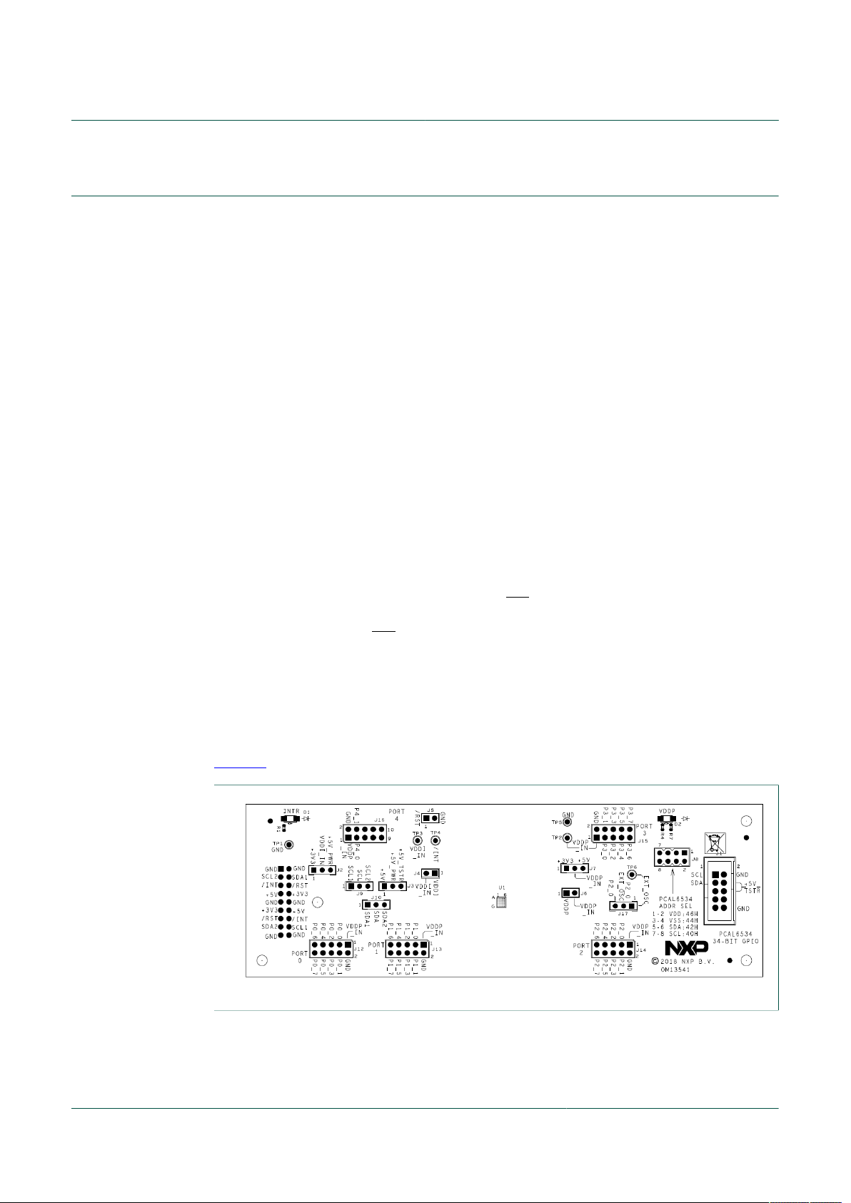
3.4 Board layout viewer
Figure 1 shows all jumper locations and labels on PCB.
Figure 1. PCAL6534 demo board layout and Labels
UM11099 All information provided in this document is subject to legal disclaimers. © NXP B.V. 2019. All rights reserved.
User manual Rev. 1.0 — 1 August 2019
5 / 29
Page 6
NXP Semiconductors
3.5 Connector pinouts
• J1 (10-pin male tester connector) is connected to master which is driving either I2C-
bus for PCAL6534. This is easily achieved with third party development tools from Total
Phase (http://www.totalphase.com). There are two tools called Aardvark and Beagle
that direct connect to this board through J1.
Table 1. J1 10-pin tester connector
J1 Pin # Function Board connection
1 SCL U1 pin A3 (PCAL6534)
2,10 GND Ground
3 SDA U1 pin A2 (PCAL6544)
4, 6 +5V_TSTR J13 pin 3
5 SDOUT (MISO) NC
7 SCLK NC
8 SDIN (MOSI) NC
9 /CS (SS) NC
UM11099
PCAL6534 demonstration board OM13541
Note: Since SDA and SCL are both connected to the device (U1) under test, the
Aardvark and the Fm+ Development board cannot be used simultaneously. The Beagle,
a bus sniffer, does not have any issues.
• J11 (18-pin female connector) can connect directly to the OM13260 Fm+ Development
board. This connector provides power, I2C signals and other ancillary signals.
Table 2. J11 18-pin Fm+ board connector
J11 Pin # Function Board connection
1, 2, 9, 10, 17, 18 GND Ground
3 SCL2 SCL Bus 2 to J9 pin 3
4 SDA1 SDA Bus 1 to J10 pin 1
5, 14 INT Interrupt to U1 pin B1, LED (D1) and TP4 (test point 4)
6, 13 RESET U1 pin A5 and J5 pin 1
7, 12 +5V J3 pin 1
8, 11 +3V3 J2 pin 1 and J7 pin 1
15 SDA2 SDA Bus 2 to J10 pin 3
16 SCL1 SCL Bus 1 to J9 pin 1
Note: The connector on the Fm+ board is a male, shrouded 14 pin types, while the
connector on this 34-bit GPIO board is an 18-pin female. The reason lies with the shroud
around the 14-pin connector. To ensure correct mating of the female with the male, two
pin positions on both female sides are grounded.
• J12, J13, J14, J15, J16 (10-pin male connector) is connected to GPIO target board
(OM13303) which consists of eight LEDs and eight switches and connects directly to
this 34-bit GPIO board through J12 (I/O of port 0), J13 (I/O of port 1), J14 (I/O of port
2), J15 (I/O of port 3), J16 (I/O of port 4). These switches and LEDs on GPIO target
board permit easy exercise of the I/O functionality of the device under test. The LEDs
light red when the voltage on that channel is below VDDP x 0.3V and LEDs light green
UM11099 All information provided in this document is subject to legal disclaimers. © NXP B.V. 2019. All rights reserved.
User manual Rev. 1.0 — 1 August 2019
6 / 29
Page 7
NXP Semiconductors
UM11099
PCAL6534 demonstration board OM13541
when the voltage is above VDDP x 0.7V. The LEDs remain off when the voltage is
between those two levels.
Table 3. J12, J13, J14, J15, J16 10-pin GPIO target board connector
J[12:16] pin # Function Board connection
1 VDDP_IN J7 pin 2 and TP2 (test point 2) and by J6 to VDDP (U1 pin A6)
2 GND Ground
3 P[0:4]_0 (I/O 0) U1 pin C1, D3, E3, E6, B5
4 P[0:4]_1 (I/O 1) U1 pin B2, F1, F4, E4, B4
5 P[0:4]_2 (I/O 2) U1 pin B3, E2, G5, D5
6 P[0:4]_3 (I/O 3) U1 pin D1, G1, G5, D6
7 P[0:4]_4 (I/O 4) U1 pin C2, G2, G6, D4
8 P[0:4]_5 (I/O 5) U1 pin C3, F2, F6, C5
9 P[0:4]_6 (I/O 6) U1 pin E1, G3, F5, C6
10 P[0:4]_7 (I/O 7) U1 pin D2, F3, E5, C4
3.6 All jumpers default setting and test points
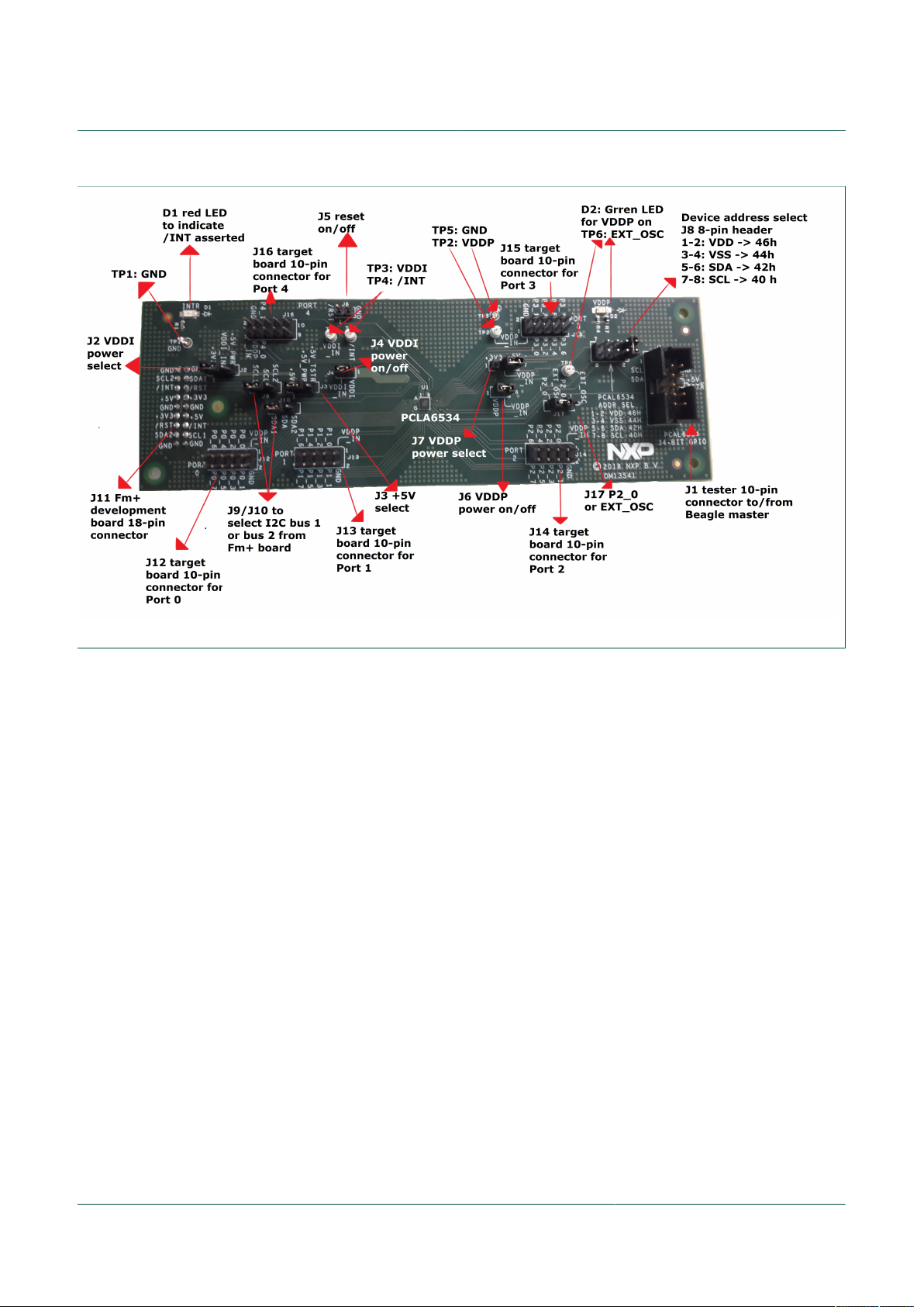
Figure 2 shows the PCAL6534 demo board.
• D1 (red LED) is connected to interrupt output (U1 pin B1), it is ON when INT is
asserted
• TP4 (INT) is connected to interrupt output (U1 pin B1) for probing use.
• TP1 and TP5 are GND test points for probing use.
• TP6 (EXT_OSC) is external clock input through J17 (1-2) to P2_0 (pin E3) for
debouncer circuit use
• TP2 (VDDP_IN) and TP3 (VDDI) are connected to external power inputs.
• All jumpers default settings and functions are shown in Table 4.
Table 4. All jumpers setting for test and evaluation
Jumper Default setting Comment
J7 (3-pin) 2-3 (VDDP_IN = +5V_
PWR)
J2 (3-pin) 1-2 (VDDI_IN = +3V3) This jumper is used to select VDDI for U1device VDDI (pin A1)
J3 (3-pin) 1-2 (+5V = +5V_PWR) This jumper is used to select +5V_PWR source
J4 (2-pin) Short Short: connect VDDI to U1 device VDDI (pin A1)
J5 (2-pin) Open Short: force /RESET (U1 pin A5) to GND
J6 (2-pin) Short Short: connect VDDP_IN to U1 device VDDP (pin A6)
This jumper is used to select VDDP for U1 device (pin A6)
1-2: select +3V3
2-3: select +5V_PWR
1-2: select +3V3 (from Fm+ development board)
2-3: select +5V_PWR
1-2: select +5V from Fm+ development board
2-3: select +5V_TSTR from tester (beagle) board
Open: connect current meter to measure the IDDI on U1 device
Open: 10K pull-up /RESET (U1 pin A5) to VDDI
Open: connect current meter to measure the IDDP on U1 device
UM11099 All information provided in this document is subject to legal disclaimers. © NXP B.V. 2019. All rights reserved.
User manual Rev. 1.0 — 1 August 2019
7 / 29
Page 8

NXP Semiconductors
UM11099
PCAL6534 demonstration board OM13541
Jumper Default setting Comment
J8 (4x2-pin) 1-2 (VDDI)*note1 This 4x2 jumper is used to select input value for ADDR (U1 pin A4)
1-2: select VDDI (address is 0x46 for PCAL6534)
3-4: select VSS (address is 0x44 for PCAL6534)
5-6: select SDA (address is 0x42 for PCAL6534)
7-8: select SCL (address is 0x40 for PCAL6534)
J9 (3-pin) 1-2 (SCL = SCL1) This jumper is used to select SCL source for U1 device (pin A3)
1-2: select SCL1 (bus 1 from Fm+ development board)
2-3: select SCL2 (bus 2 from Fm+ development board)
J10 (3-pin) 1-2 (SDA = SDA1) This jumper is used to select SDA source for U1 device (pin A2)
1-2: select SDA1 (bus 1 from Fm+ development board)
2-3: select SDA2 (bus 2 from Fm+ development board)
J11 (18-pin) Connect Fm+
development board
J12-J16 (10-pin) Connect to GPIO
Target board
J17 (3-pin) 2-3 (P2_0) This jumper is used to select function either P2_0 or EXT_OSC for U1
1. Default PCAL6534 slave address is set to 0x46 (ADDR = VDD)
This 18-pin female connect to PORT A/B/C/D (14-pin male) on Fm+
development board (OM13260) for power supply, I2C-bus and control
signals to test
This 10-pin male connect to GPIO target board (OM13303) for input/
output pins test
device (pin E3)
1-2: select external oscillator (EXT_OSC) input for debounce circuit use
2-3: select P2_0 input as normal operation
Figure 2. PCAL6534 demo board (OM13541)
UM11099 All information provided in this document is subject to legal disclaimers. © NXP B.V. 2019. All rights reserved.
User manual Rev. 1.0 — 1 August 2019
8 / 29
Page 9
NXP Semiconductors
UM11099
PCAL6534 demonstration board OM13541
Figure 3. PCAL6534 demo board (OM13541) detailed
UM11099 All information provided in this document is subject to legal disclaimers. © NXP B.V. 2019. All rights reserved.
User manual Rev. 1.0 — 1 August 2019
9 / 29
Page 10

NXP Semiconductors
5
5
4
4
3
3
2
2
1
1
D D
C C
B B
A A
External power inputs:
VDDP_IN: J7 -> open
VDDI_IN: J2 -> open
J3
+5V_PWR source
1-2: Fm+ Develp board
2-3: +5V_TSTR from tester (beagle)
board
J2
VDDI_IN source
1-2: 3.3v from Fm+ board
2-3: +5V_PWR
J5:
Short: force /RESET (U1 pin A5) to GND
Open: 10K pull-up /RESET (U1 pin A5) to VDDI
J6:
Short: connect VDDP_IN to U1 device VDDP
(pin A6)
Open: connect current meter to measure the
IDDP on U1 device
GND
PCAL6534 address select:
1-2 (VDDI) : 46h
3-4 (VSS) : 44h
5-6 (SDA) : 42h
7-8 (SCL) : 40h
VDDP SELECCION
RESET
I2C BUS SELECTION
EXTERNAL OSCILLATOR SELECION
J[12:16] connect to OM13303 GPIO target board which consists
ofeight LEDs and eight switches for each I/O pin test
TESTPOINTS
CONNECTORS
POWER SUPPLY SELECTION
PORT 0 PORT 1 PORT 2 PORT 3 PORT 4
P2_0 function select
1-2: Ext. debounce clock input
2-3: Normal P2_0 port
10-pin male header connector
to/from Beagle master (I2C or
SPI) to drive the PCAL6534
VDDP Indicator
18-pin female header connector to/from
the Fm+ development board (OM13260)
master to provide power, I2C signals
and other control signals
J4
Short: connect VDDI to U1 device
VDDI (pin A1)
Open: connect current meter to
measure the IDDI on U1 device
INTR Indicator
OM13541: PCAL6534EV 34-Bit Fm+ I2C-bus GPIO test & demo board
J7:
This jumper is used to select VDDP for U1 device
(pin A6)
1-2: select +3V3
2-3: select +5V_PWR
J10:
This jumper is used to select SDA source for U1
device (pin A2)
1-2: select SDA1 (bus 1 from Fm+ development board)
2-3: select SDA2 (bus 2 from Fm+ development board)
J9:
This jumper is used to select SCL source for U1
device (pin A3)
1-2: select SCL1 (bus 1 from Fm+ development board)
2-3: select SCL2 (bus 2 from Fm+ development board)
+5V_TSTR
+5V_TSTR
+5V
+5V_PWR
+3V3
VDDI_IN VDDI
VDDI_IN
VDDI_IN
+3V3 +5V_PWR
VDDI_IN
VDDP_IN VDDP_IN VDDP_IN VDDP_IN VDDP_IN
VDDP_IN
+5V
+3V3
+3V3
+5V
VDDI
VDDP_IN
VDDI_IN
Drawing Title:
Size Document Number Rev
Date: Sheet
of
Page Title:
ICAP Classification: CP: IUO: PUBI:
SCH-32015 PDF: SPF-32015 A
OM13541SKT
C
Monday, February 26, 2018
PCAL6534
3 3
___ ___
X
Drawing Title:
Size Document Number Rev
Date: Sheet
of
Page Title:
ICAP Classification: CP: IUO: PUBI:
SCH-32015 PDF: SPF-32015 A
OM13541SKT
C
Monday, February 26, 2018
PCAL6534
3 3
___ ___
X
Drawing Title:
Size Document Number Rev
Date: Sheet
of
Page Title:
ICAP Classification: CP: IUO: PUBI:
SCH-32015 PDF: SPF-32015 A
OM13541SKT
C
Monday, February 26, 2018
PCAL6534
3 3
___ ___
X
J8
M20-9980446
1 2
3 4
65
7 8
J3
HDR_1X3
1
2
3
TP4
J15
HDR_2X5
12
34
6 5
78
910
TP2
TP1
J7
HDR_1X3
1
2
3
J2
HDR_1X3
1
2
3
J4
HDR_1X2
1
2
R1
1K
J1
5103308-1
12
34
6 5
78
910
+
C1
4.7uF
J14
HDR_2X5
12
34
6 5
78
910
D2
GREEN
AC
TP5
R2
10K
C2
0.1uF
J13
HDR_2X5
12
34
6 5
78
910
J6
HDR_1X2
1
2
J9
HDR_1X3
1
2
3
TP3
J12
HDR_2X5
12
34
6 5
78
910
D1
RED
AC
C4
0.1uF
R4
1K
J10
HDR_1X3
1
2
3
R7
AVR-M1608C080MTAAB
12
J11
CON_2X9
1 2
3 4
65
7 8
9 10
11 12
13 14
15 16
17 18
TP6
U1
PCAL6534 + SKT_BGA42
SCL
A3
SDA
A2
VDD_I2C_BUS
A1
INT
B1
P0_0
C1
P0_1
B2
P0_2
B3
P0_3
D1
P0_4
C2
P0_5
C3
P0_6
E1
P0_7
D2
P1_0
D3
P1_1
F1
P1_2
E2
P1_3
G1
P1_4
G2
P1_5
F2
P1_6
G3
P1_7
F3
P4_0
B5
P4_1
B4
ADDR
A4
VSS
B6
VDD
A6
RESET
A5
P3_0
E6
P3_1
E4
P3_2
D5
P3_3
D6
P3_4
D4
P3_5
C5
P3_6
C6
P3_7
C4
P2_0
E3
P2_1
F4
P2_2
G4
P2_3
G5
P2_4
G6
P2_5
F6
P2_6
F5
P2_7
E5
+
C3
4.7uF
R6
10K
R5
10K
J5
HDR_1X2
1
2
J16
HDR_2X5
12
34
6 5
78
910
J17
HDR_1X3
1
2
3
SDA
SCL
/INT
ADDR
SDA
SCL
SDA1
SDA2
SCL2
SCL1
GND
SCL2
SDA2
/RESET
/INT
SDA1
/RESET
/INT
SCL1
P0_7
P0_5
P0_3
P0_1 P0_0
P0_2
P0_4
P0_6 P1_7
P1_5
P1_3
P1_1 P1_0
P1_2
P1_4
P1_6 P2_7
P2_5
P2_3
P2_1 P2_0
P2_2
P2_4
P2_6
P2_0/EXT_OSC
EXT_OSC
P3_7
P3_5
P3_3
P3_1 P3_0
P3_2
P3_4
P3_6
P4_1 P4_0
P2_0
/RESET
VDDP
VDDP
SDA
SCL
/INT
ADDR
/RESET
P0_0
P0_1
P0_2
P0_3
P0_4
P0_5
P0_6
P0_7
P1_0
P1_1
P1_2
P1_3
P1_4
P1_5
P1_6
P1_7
P2_0/EXT_OSC
P2_1
P2_2
P2_3
P2_4
P2_5
P2_6
P2_7
P3_0
P3_1
P3_2
P3_3
P3_4
P3_5
P3_6
P3_7
P4_0
P4_1
UM11099
PCAL6534 demonstration board OM13541
4 Schematic
Figure 4. PCAL6534 demo board schematic
UM11099 All information provided in this document is subject to legal disclaimers. © NXP B.V. 2019. All rights reserved.
User manual Rev. 1.0 — 1 August 2019
10 / 29
Page 11

NXP Semiconductors
5 Installation
5.1 PCAL6534 demo board, Fm+ development board, GPIO target board
The OM13541 PCAL6534 34-bit GPIO demo board is a daughter card to the OM13260
Fm+ I2C bus development board, which is part of the Fm+ development board kit
(OM13320); three I/O ports (8-bit × 3) on PCAL6534 are connected to the GPIO target
board for I/O visualization. You may download the software, user manual, and find
ordering information at the NXP web site:
https://www.nxp.com/products/analog/interfaces/ic-bus/ic-led-controllers/ic-fm-plusdevelopment-board:OM13320
5.2 OM13541 connection to Fm+ I2C-bus development board
The OM13260 Fm+ I2C-bus development board should be disconnected from your PC
before mounting the OM13541 board with GPIO target board on to it. The OM13541
board has an 18-pin female connector (J11) that connects to CN4 14-pin male connector
on the Fm+ development board (OM13260) as shown in Figure 5. Five GPIO Target
boards (OM13303) through ribbon cables connect to 10-pin male connectors (J12, J13,
J14, J15, J16) on OM13541 PCAL6534 34-bit GPIO demo board for 8-bit I/O port0,
port1, port2, port3 and port4.
UM11099
PCAL6534 demonstration board OM13541
Figure 5. PCAL6534 demo board (OM13541) mounting to the Fm+ development board (OM13260) and connecting
to five GPIO target boards (OM13303)
UM11099 All information provided in this document is subject to legal disclaimers. © NXP B.V. 2019. All rights reserved.
User manual Rev. 1.0 — 1 August 2019
11 / 29
Page 12

NXP Semiconductors
PCAL6534 demonstration board OM13541
6 PCAL6534 evaluation steps with Fm+ development board
The PCAL6534 is controlled by the Fm+ development board GUI in Expert mode as
shown in Figure 6 and Figure 7.
UM11099
Figure 6. Select the Expert Mode from Fm+ development board GUI (1 of 2)
UM11099 All information provided in this document is subject to legal disclaimers. © NXP B.V. 2019. All rights reserved.
User manual Rev. 1.0 — 1 August 2019
12 / 29
Page 13

NXP Semiconductors
UM11099
PCAL6534 demonstration board OM13541
Figure 7. Select the Expert Mode from Fm+ development board GUI (2 of 2)
Connect the hardware as described in Section 5.2. All jumpers are in default setting and
device address is set to 0x46h on J8 (set ADDR = VDDI) for PCAL6534 demo board.
When you have correctly installed the software and the demonstration board hardware is
connected and recognized by the computer, start the Fm+ development board software.
As shown in Figure 7, when the demonstration board hardware is correctly connected
to the USB port and the computer recognizes it, the message “USB-I2C Hardware
Detected” is displayed on the bottom of the window.
6.1 PCAL6534 output shifting pattern demo for all five ports
1. From the ‘Device’ drop-down menus select ‘Expert Mode’ as shown in Figure 7.
2. Copy the “output shifting pattern on all five ports” text file as shown below. From the
‘File’ drop-down menus select ‘Open’, and from the “open data file” window to select
the “output shifting pattern on all five ports” text file.
========================================================================
Expert Mode Data File
46,Write,Yes,200,0F,00,00,00,00,00,Comments: set all GPIOs as output ports
46,Write,Yes,200,05,FF,FF,FF,FF,FF,Comments: write registers 04,05,06 to set all
output ports to 1s
46,Write,Yes,200,05,FE,FE,FE,FE,FE,Comments: set bit0 to 0 in all five ports
46,Write,Yes,200,05,FD,FD,FD,FD,FD,Comments: set bit1 to 0 in all five ports
UM11099 All information provided in this document is subject to legal disclaimers. © NXP B.V. 2019. All rights reserved.
User manual Rev. 1.0 — 1 August 2019
13 / 29
Page 14

NXP Semiconductors
46,Write,Yes,200,05,FB,FB,FB,FB,Comments: set bit2 to 0 in Ports 0 to 3
46,Write,Yes,200,05,F7,F7,F7,F7,Comments: set bit3 to 0 in Ports 0 to 3
46,Write,Yes,200,05,EF,EF,EF,EF,Comments: set bit4 to 0 in Ports 0 to 3
46,Write,Yes,200,05,DF,DF,DF,DF,Comments: set bit5 to 0 in Ports 0 to 3
46,Write,Yes,200,05,BF,BF,BF,BF,Comments: set bit6 to 0 in Ports 0 to 3
46,Write,Yes,200,05,7F,7F,7F,7F,Comments: set bit7 to 0 in Ports 0 to 3
Sequence:01,02,03,04,05,06,07,08,09,10
=========================================================================
3. After opening the “output shifting pattern on all five ports” text file, the “NXP Fm+
Board GUI” in Expert mode screen is displayed as shown in Figure 8.
4. Click the ‘Send All’ button; all the valid messages on the screen are sent in the order
of the row number (Msg #). This action is performed once.
UM11099
PCAL6534 demonstration board OM13541
Figure 8. Message data in Expert mode to demo “output shifting pattern on all five ports”
6.2 PCAL6534 registers are controlled by Fm+ board GUI
1. Select 34-bit PCAL6534 from I/O Expanders as shown in Figure 9.
UM11099 All information provided in this document is subject to legal disclaimers. © NXP B.V. 2019. All rights reserved.
User manual Rev. 1.0 — 1 August 2019
14 / 29
Page 15

NXP Semiconductors
UM11099
PCAL6534 demonstration board OM13541
Figure 9. Device selection screen for PCAL6534
2. Input registers read are shown in Figure 10.
Figure 10. Device configuration screen for registers 00-04 hex
3. Output registers read or write are shown in Figure 11.
UM11099 All information provided in this document is subject to legal disclaimers. © NXP B.V. 2019. All rights reserved.
User manual Rev. 1.0 — 1 August 2019
15 / 29
Page 16

NXP Semiconductors
UM11099
PCAL6534 demonstration board OM13541
Figure 11. Device configuration screen for registers 05-09 hex
4. Polarity registers read or write are shown in Figure 12.
Figure 12. Device configuration screen for registers 0A-0E hex
5. Port Configuration registers read or write are shown in Figure 13.
UM11099 All information provided in this document is subject to legal disclaimers. © NXP B.V. 2019. All rights reserved.
User manual Rev. 1.0 — 1 August 2019
16 / 29
Page 17

NXP Semiconductors
UM11099
PCAL6534 demonstration board OM13541
Figure 13. Device configuration screen for registers 0F-13 hex
6. Drive strength registers read or write are shown in Figure 14.
Figure 14. Device configuration screen for registers 30-38 hex
7. Input latch registers read or write are shown in Figure 15.
UM11099 All information provided in this document is subject to legal disclaimers. © NXP B.V. 2019. All rights reserved.
User manual Rev. 1.0 — 1 August 2019
17 / 29
Page 18

NXP Semiconductors
UM11099
PCAL6534 demonstration board OM13541
Figure 15. Device configuration screen for registers 3A-3E hex
8. PU/PD Enable registers read or write are shown in Figure 16.
Figure 16. Device configuration screen for registers 3F-43 hex
9. PU/PD select registers read or write are shown in Figure 17.
UM11099 All information provided in this document is subject to legal disclaimers. © NXP B.V. 2019. All rights reserved.
User manual Rev. 1.0 — 1 August 2019
18 / 29
Page 19

NXP Semiconductors
UM11099
PCAL6534 demonstration board OM13541
Figure 17. Device configuration screen for registers 44-48 hex
10.Interrupt mask registers read or write are shown in Figure 18.
Figure 18. Device configuration screen for registers 49-4D hex
11.Output port configuration register read or write is shown in Figure 19.
UM11099 All information provided in this document is subject to legal disclaimers. © NXP B.V. 2019. All rights reserved.
User manual Rev. 1.0 — 1 August 2019
19 / 29
Page 20

NXP Semiconductors
UM11099
PCAL6534 demonstration board OM13541
Figure 19. Device configuration screen for registers 53 hex
12.Interrupt edge registers read or write are shown in Figure 20.
Figure 20. Device configuration screen for registers 54-5C hex
13.Interrupt Clear registers write are shown in Figure 21.
UM11099 All information provided in this document is subject to legal disclaimers. © NXP B.V. 2019. All rights reserved.
User manual Rev. 1.0 — 1 August 2019
20 / 29
Page 21

NXP Semiconductors
UM11099
PCAL6534 demonstration board OM13541
Figure 21. Device configuration screen for registers 5E-62 hex
14.Input status registers read are shown in Figure 22.
Figure 22. Device configuration screen for registers 63-67 hex
15.Pin Configuration registers read or write are shown in Figure 23.
UM11099 All information provided in this document is subject to legal disclaimers. © NXP B.V. 2019. All rights reserved.
User manual Rev. 1.0 — 1 August 2019
21 / 29
Page 22

NXP Semiconductors
UM11099
PCAL6534 demonstration board OM13541
Figure 23. Device configuration screen for registers 68-6C hex
16.Debounce registers read or write are shown in Figure 24.
Figure 24. Device configuration screen for registers 6D-6F hex
UM11099 All information provided in this document is subject to legal disclaimers. © NXP B.V. 2019. All rights reserved.
User manual Rev. 1.0 — 1 August 2019
22 / 29
Page 23

NXP Semiconductors
7 Support
For support, please send an E-mail to: i2c.support@nxp.com
UM11099
PCAL6534 demonstration board OM13541
UM11099 All information provided in this document is subject to legal disclaimers. © NXP B.V. 2019. All rights reserved.
User manual Rev. 1.0 — 1 August 2019
23 / 29
Page 24

NXP Semiconductors
8 Abbreviations
Table 5. Abbreviations
Acronym Description
ESD Electro Static Discharge
GPIO General Purpose Input/Output
GUI Graphical User Interface
I2C-bus Inter-integrated Circuit bus
LED Light Emitting Diode
PC Personal Computer
PCB Printed-Circuit Board
SMBus System Management Bus
USB Universal Serial Bus
UM11099
PCAL6534 demonstration board OM13541
UM11099 All information provided in this document is subject to legal disclaimers. © NXP B.V. 2019. All rights reserved.
User manual Rev. 1.0 — 1 August 2019
24 / 29
Page 25

NXP Semiconductors
9 References
1. PCAL6534, Ultra low-voltage translating 34-bit Fm+ I2C-bus/SMBus I/O expander;
Product data sheet; NXP Semiconductors
2. UM10741, Fm+ Development Kit OM13320 User manual; NXP Semiconductors
UM11099
PCAL6534 demonstration board OM13541
UM11099 All information provided in this document is subject to legal disclaimers. © NXP B.V. 2019. All rights reserved.
User manual Rev. 1.0 — 1 August 2019
25 / 29
Page 26

NXP Semiconductors
10 Legal information
10.1 Definitions
Draft — The document is a draft version only. The content is still under
internal review and subject to formal approval, which may result in
modifications or additions. NXP Semiconductors does not give any
representations or warranties as to the accuracy or completeness of
information included herein and shall have no liability for the consequences
of use of such information.
10.2 Disclaimers
Limited warranty and liability — Information in this document is believed
to be accurate and reliable. However, NXP Semiconductors does not
give any representations or warranties, expressed or implied, as to the
accuracy or completeness of such information and shall have no liability
for the consequences of use of such information. NXP Semiconductors
takes no responsibility for the content in this document if provided by an
information source outside of NXP Semiconductors. In no event shall NXP
Semiconductors be liable for any indirect, incidental, punitive, special or
consequential damages (including - without limitation - lost profits, lost
savings, business interruption, costs related to the removal or replacement
of any products or rework charges) whether or not such damages are based
on tort (including negligence), warranty, breach of contract or any other
legal theory. Notwithstanding any damages that customer might incur for
any reason whatsoever, NXP Semiconductors’ aggregate and cumulative
liability towards customer for the products described herein shall be limited
in accordance with the Terms and conditions of commercial sale of NXP
Semiconductors.
Right to make changes — NXP Semiconductors reserves the right to
make changes to information published in this document, including without
limitation specifications and product descriptions, at any time and without
notice. This document supersedes and replaces all information supplied prior
to the publication hereof.
Suitability for use — NXP Semiconductors products are not designed,
authorized or warranted to be suitable for use in life support, life-critical or
safety-critical systems or equipment, nor in applications where failure or
malfunction of an NXP Semiconductors product can reasonably be expected
to result in personal injury, death or severe property or environmental
damage. NXP Semiconductors and its suppliers accept no liability for
inclusion and/or use of NXP Semiconductors products in such equipment or
applications and therefore such inclusion and/or use is at the customer’s own
risk.
UM11099
PCAL6534 demonstration board OM13541
products using NXP Semiconductors products, and NXP Semiconductors
accepts no liability for any assistance with applications or customer product
design. It is customer’s sole responsibility to determine whether the NXP
Semiconductors product is suitable and fit for the customer’s applications
and products planned, as well as for the planned application and use of
customer’s third party customer(s). Customers should provide appropriate
design and operating safeguards to minimize the risks associated with
their applications and products. NXP Semiconductors does not accept any
liability related to any default, damage, costs or problem which is based
on any weakness or default in the customer’s applications or products, or
the application or use by customer’s third party customer(s). Customer is
responsible for doing all necessary testing for the customer’s applications
and products using NXP Semiconductors products in order to avoid a
default of the applications and the products or of the application or use by
customer’s third party customer(s). NXP does not accept any liability in this
respect.
Export control — This document as well as the item(s) described herein
may be subject to export control regulations. Export might require a prior
authorization from competent authorities.
Evaluation products — This product is provided on an “as is” and “with all
faults” basis for evaluation purposes only. NXP Semiconductors, its affiliates
and their suppliers expressly disclaim all warranties, whether express,
implied or statutory, including but not limited to the implied warranties of
non-infringement, merchantability and fitness for a particular purpose. The
entire risk as to the quality, or arising out of the use or performance, of this
product remains with customer. In no event shall NXP Semiconductors, its
affiliates or their suppliers be liable to customer for any special, indirect,
consequential, punitive or incidental damages (including without limitation
damages for loss of business, business interruption, loss of use, loss of
data or information, and the like) arising out the use of or inability to use
the product, whether or not based on tort (including negligence), strict
liability, breach of contract, breach of warranty or any other theory, even if
advised of the possibility of such damages. Notwithstanding any damages
that customer might incur for any reason whatsoever (including without
limitation, all damages referenced above and all direct or general damages),
the entire liability of NXP Semiconductors, its affiliates and their suppliers
and customer’s exclusive remedy for all of the foregoing shall be limited to
actual damages incurred by customer based on reasonable reliance up to
the greater of the amount actually paid by customer for the product or five
dollars (US$5.00). The foregoing limitations, exclusions and disclaimers
shall apply to the maximum extent permitted by applicable law, even if any
remedy fails of its essential purpose.
Translations — A non-English (translated) version of a document is for
reference only. The English version shall prevail in case of any discrepancy
between the translated and English versions.
Applications — Applications that are described herein for any of these
products are for illustrative purposes only. NXP Semiconductors makes
no representation or warranty that such applications will be suitable
for the specified use without further testing or modification. Customers
are responsible for the design and operation of their applications and
UM11099 All information provided in this document is subject to legal disclaimers. © NXP B.V. 2019. All rights reserved.
10.3 Trademarks
Notice: All referenced brands, product names, service names and
trademarks are the property of their respective owners.
User manual Rev. 1.0 — 1 August 2019
26 / 29
Page 27

NXP Semiconductors
Tables
UM11099
PCAL6534 demonstration board OM13541
Tab. 1. J1 10-pin tester connector ................................ 6
Tab. 2. J11 18-pin Fm+ board connector ...................... 6
Tab. 3. J12, J13, J14, J15, J16 10-pin GPIO target
board connector ................................................ 7
Tab. 4. All jumpers setting for test and evaluation .........7
Tab. 5. Abbreviations ...................................................24
UM11099 All information provided in this document is subject to legal disclaimers. © NXP B.V. 2019. All rights reserved.
User manual Rev. 1.0 — 1 August 2019
27 / 29
Page 28

NXP Semiconductors
Figures
UM11099
PCAL6534 demonstration board OM13541
Fig. 1. PCAL6534 demo board layout and Labels ........5
Fig. 2. PCAL6534 demo board (OM13541) ..................8
Fig. 3. PCAL6534 demo board (OM13541) detailed .... 9
Fig. 4. PCAL6534 demo board schematic ..................10
Fig. 5. PCAL6534 demo board (OM13541)
mounting to the Fm+ development board
(OM13260) and connecting to five GPIO
target boards (OM13303) ................................ 11
Fig. 6. Select the Expert Mode from Fm+
development board GUI (1 of 2) ..................... 12
Fig. 7. Select the Expert Mode from Fm+
development board GUI (2 of 2) ..................... 13
Fig. 8. Message data in Expert mode to demo
“output shifting pattern on all five ports” .......... 14
Fig. 9. Device selection screen for PCAL6534 ........... 15
Fig. 10. Device configuration screen for registers
00-04 hex ........................................................ 15
Fig. 11. Device configuration screen for registers
05-09 hex ........................................................ 16
Fig. 12. Device configuration screen for registers
0A-0E hex ....................................................... 16
Fig. 13. Device configuration screen for registers
0F-13 hex ........................................................17
Fig. 14. Device configuration screen for registers
30-38 hex ........................................................ 17
Fig. 15. Device configuration screen for registers
3A-3E hex ....................................................... 18
Fig. 16. Device configuration screen for registers
3F-43 hex ........................................................18
Fig. 17. Device configuration screen for registers
44-48 hex ........................................................ 19
Fig. 18. Device configuration screen for registers
49-4D hex ........................................................19
Fig. 19. Device configuration screen for registers 53
hex ...................................................................20
Fig. 20. Device configuration screen for registers
54-5C hex ........................................................20
Fig. 21. Device configuration screen for registers
5E-62 hex ........................................................21
Fig. 22. Device configuration screen for registers
63-67 hex ........................................................ 21
Fig. 23. Device configuration screen for registers
68-6C hex ........................................................22
Fig. 24. Device configuration screen for registers
6D-6F hex ....................................................... 22
UM11099 All information provided in this document is subject to legal disclaimers. © NXP B.V. 2019. All rights reserved.
User manual Rev. 1.0 — 1 August 2019
28 / 29
Page 29

NXP Semiconductors
Contents
1 Introduction ......................................................... 3
2 Features of the OM13541 34-bit GPIO
daughter board ....................................................4
3 Hardware description ......................................... 5
3.1 Power supply jumpers ....................................... 5
3.2 SCL and SDA jumpers ...................................... 5
3.3 Device reset, interrupt and address pin
selection .............................................................5
3.4 Board layout viewer ...........................................5
3.5 Connector pinouts ............................................. 6
3.6 All jumpers default setting and test points ......... 7
4 Schematic .......................................................... 10
5 Installation ......................................................... 11
5.1 PCAL6534 demo board, Fm+ development
board, GPIO target board ................................11
5.2 OM13541 connection to Fm+ I2C-bus
development board .......................................... 11
6 PCAL6534 evaluation steps with Fm+
development board ........................................... 12
6.1 PCAL6534 output shifting pattern demo for
all five ports ..................................................... 13
6.2 PCAL6534 registers are controlled by Fm+
board GUI ........................................................14
7 Support ...............................................................23
8 Abbreviations .................................................... 24
9 References ......................................................... 25
10 Legal information ..............................................26
UM11099
PCAL6534 demonstration board OM13541
Please be aware that important notices concerning this document and the product(s)
described herein, have been included in section 'Legal information'.
© NXP B.V. 2019. All rights reserved.
For more information, please visit: http://www.nxp.com
For sales office addresses, please send an email to: salesaddresses@nxp.com
Date of release: 1 August 2019
Document identifier: UM11099
 Loading...