

Page 1
SECURITY
STATUS
UM10966
NTAG I²C plus Explorer Kit - Android Demo
Rev. 2.1 — 09 March 2017
360121
User manual
COMPANY PUBLIC
Document information
Info
Content
Keywords
NTAG I2C plus, Explorer Kit, Android, NFC tag
Abstract
This User Manual describes the functionalities and how to use the
and have the same look and
Android and PC application of the NTAG I2C plus Explorer kit. Both
applications provide the same functionality
feel so this User Manual is valid for both.
Page 2

SECURITY
STATUS
NXP Semiconductors
UM10966
NTAG I²C plus Explorer Kit - Android Demo
UM10966
All information provided in this docum ent is subject to legal disclaimers.
© NXP Semiconductors N.V. 2017. All rights reserved.
User manual
COMPANY PUBLIC
Rev. 2.1 — 09 March 2017
360121
2 of 55
Contact information
For more information, please visit:
Revision history
Rev
Date
Description
2.1
20170309
Update - Bluetooth Pairing added
2.0
20170201
Updates
1.0
20160216
Initial Version
http://www.nxp.com
Page 3

SECURITY
STATUS
NXP Semiconductors
UM10966
NTAG I²C plus Explorer Kit - Android Demo
UM10966
All information provided in this docum ent is subject to legal disclaimers.
© NXP Semiconductors N.V. 2017. All rights reserved.
User manual
COMPANY PUBLIC
Rev. 2.1 — 09 March 2017
360121
3 of 55
1. Object
NTAG I2C plus Explorer kit is an all-in-one demonstr ation and development res ource to
demonstrate the unique pr operties of the NTAG I
full complement of hardware and s oftware tools, users can inv estigate the capabiliti es of
the chip through the various demonstrations, develop and test their own applications
(with additional LPC-Link2 debug probe
This User Manual ex plains how to use the NTAG I
The Windows app is not detailed in this User Manual since it provides identical
functionalities as the Android app, therefore the same User Manual is valid.
Technical aspects relat ed to the IC features are beyond the scope of this doc ument. To
get further technical details please consult the dedicated Datasheet “NTAG I
Forum Type 2 Tag compliant IC with I
1
).
2
C interface” (refer to [NTAGI2Cplus]).
2
C plus connected tag. By including a
2
C plus d emo application f or Android.
2
C plus, NFC
1
www.nxp.com/LPC-LINK2
Page 4
SECURITY
STATUS
NXP Semiconductors
UM10966
NTAG I²C plus Explorer Kit - Android Demo
UM10966
All information provided in this docum ent is subject to legal disclaimers.
© NXP Semiconductors N.V. 2017. All rights reserved.
User manual
COMPANY PUBLIC
Rev. 2.1 — 09 March 2017
360121
4 of 55
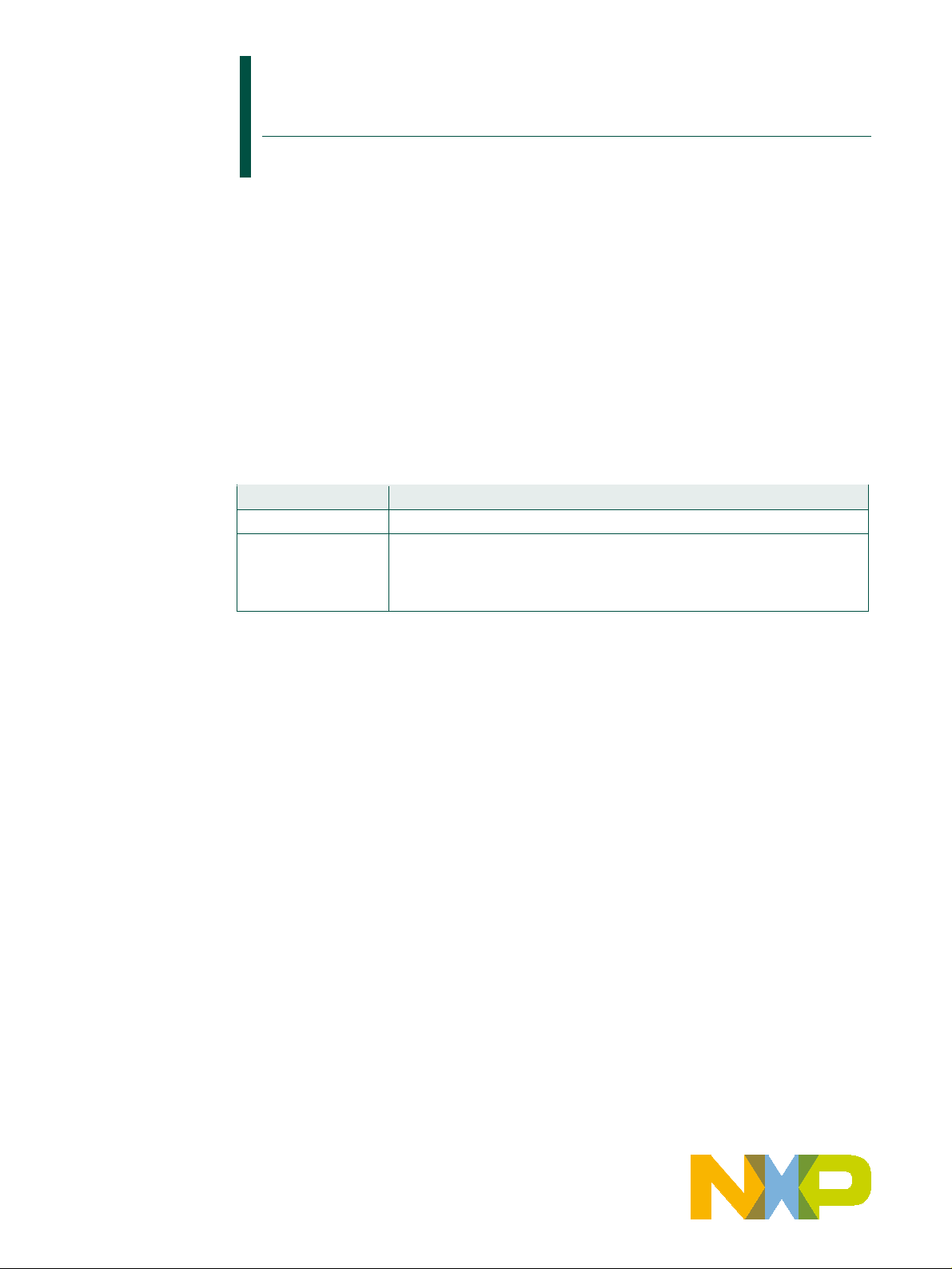
Fig 1. NTAG I2C plus
2. NT AG I2C plus introduction
The NTAG I2C plus part of NXP’s NTAG family offering both contactless and contact
interfaces. In addit ion to the passive NFC F orum compliant RF interface, the NTAG I
plus pro vides an I
when the chip is powered by an external device, i.e. a NFC mobile phone.
The NTAG I
supply external lo w power devices (e.g. microc ontrollers ) with the ener gy gener ated f rom
the RF field of the external NFC device.
2
C interface that al lows the IC to c ommunicate with the mic rocontroller
2
C plus operating in energy harvesting mode provides the possibility to
2
C
The NTAG I
1. EEPROM memory compliant with the NFC Forum Type 2 Tag implementation.
2. 64-byte SRAM memory, which is mapped to the EEPROM memory and it is
The N TAG I
of data from the RF interf ace to the I
use of the SRAM memory that allows fas t data transfer between interfaces without the
EEPROM performance limitations.
In addition to the I
Detection pin for waking up the connected host devices or synchronizing the data
transfer between the two interfaces.
The NTAG I
done by authenticating the tag with a password. When the tag is protected,
authentication is nee ded to access the memor y. The NTAG I
speed when writing into the SRAM memory.
2
C plus product has two types of memories:
externally powered.
2
C plus feat ures a pass-through mode tha t allows fas t download an d upload
2
C interface func tionalit y, the NT AG I2C plus pr oduct f eatures an Event
2
C plus offers the pos sibil ity to pr otec t the memory access. This protection is
2
C interface and vi ce versa. T his f unctional it y m akes
2
C plus also impr oves the
Page 5
SECURITY
STATUS
NXP Semiconductors
UM10966
NTAG I²C plus Explorer Kit - Android Demo
UM10966
All information provided in this docum ent is subject to legal disclaimers.
© NXP Semiconductors N.V. 2017. All rights reserved.
User manual
COMPANY PUBLIC
Rev. 2.1 — 09 March 2017
360121
5 of 55
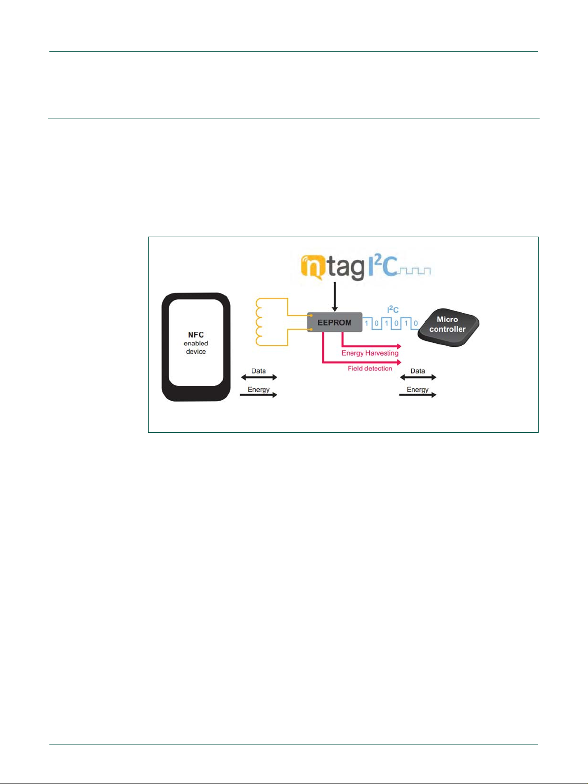
Fig 2. NTAG I2C plus Explorer Board (refer to [EXPLORER])
3. NT AG I2C plus Expl orer kit contents
The NTAG I2C plus Explorer kit (NEK) consists of hardware and software tools that
developers can use to und erstand th e NXP NTAG I
prototypes to demonstrate its potential for other application. The kit includes:
3.1 Hardware components
3.1.1 NT AG I2C plus Explorer Board
A hardware board bas ed on the NXP LPC 11U24 m icrocontroller (refer to [LPC11U24]),
with on-board LCD d isplay, NXP LM75B tem perature sensor (refer to [LM75B]), vo ltage
monitors, I2C serial bus connector, JT AG/SWD debug connector, RGD LED micro USB
connector and five push buttons.
2
C plus functionalities and c reate firs t
Page 6
SECURITY
STATUS
NXP Semiconductors
UM10966
NTAG I²C plus Explorer Kit - Android Demo
UM10966
All information provided in this docum ent is subject to legal disclaimers.
© NXP Semiconductors N.V. 2017. All rights reserved.
User manual
COMPANY PUBLIC
Rev. 2.1 — 09 March 2017
360121
6 of 55
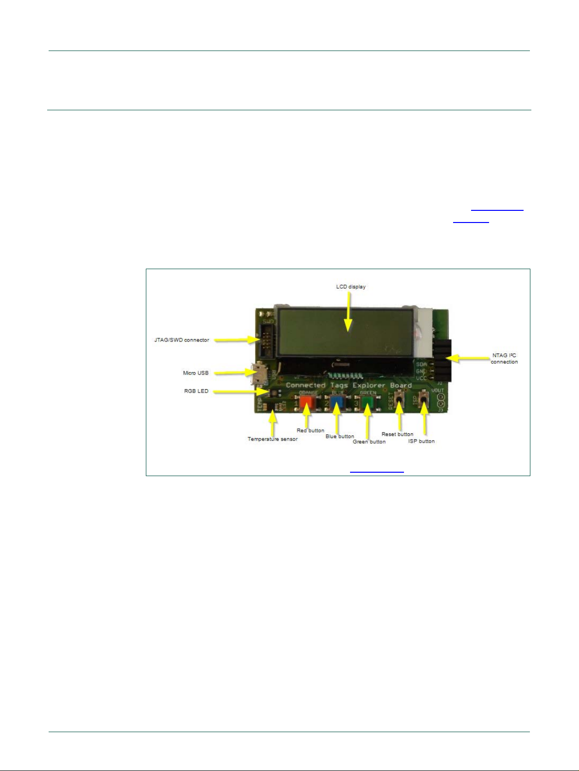
Fig 3. PCB and Flex antenna boards with NTAG I²C plus IC
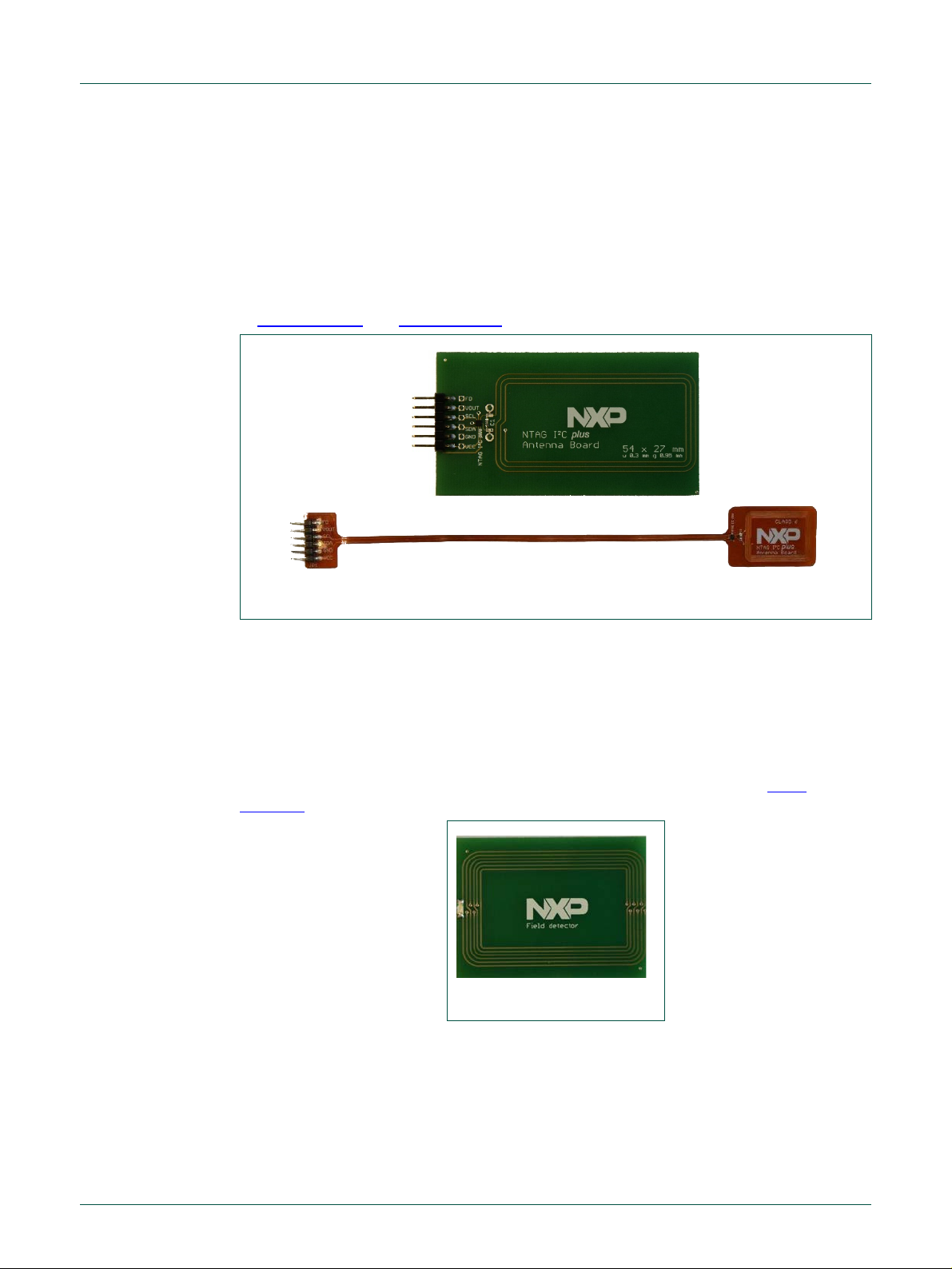
Fig 4. Field detector board
3.1.2 Antenna board
The antenna board carries the NTAG I2C plus 2k version itself and provides two
interfaces:
• The RF interface to an NFC device.
• The I
The design files for both th e PCB a nd Flex ante nna c an be f ound on the web pa ge (ref er
to [PCB Antenna] and [Flex Antenna]
2
C interface to the host, e.g. the NTAG I2C plus Explorer board.
3.1.3 Field detector board
The position of the antenna of NFC devices vary from device to device. To use the
Explorer Kit with an NFC Device, NFC radio needs to be enabled. To find the position of
the antenna, it is convenient to use the included field detector board. The LED helps to
find the antenna position.
Design files may be downloaded from the demo board homepage (refer to
Detector])
[Field
Page 7
SECURITY
STATUS
NXP Semiconductors
UM10966
NTAG I²C plus Explorer Kit - Android Demo
UM10966
All information provided in this docum ent is subject to legal disclaimers.
© NXP Semiconductors N.V. 2017. All rights reserved.
User manual
COMPANY PUBLIC
Rev. 2.1 — 09 March 2017
360121
7 of 55
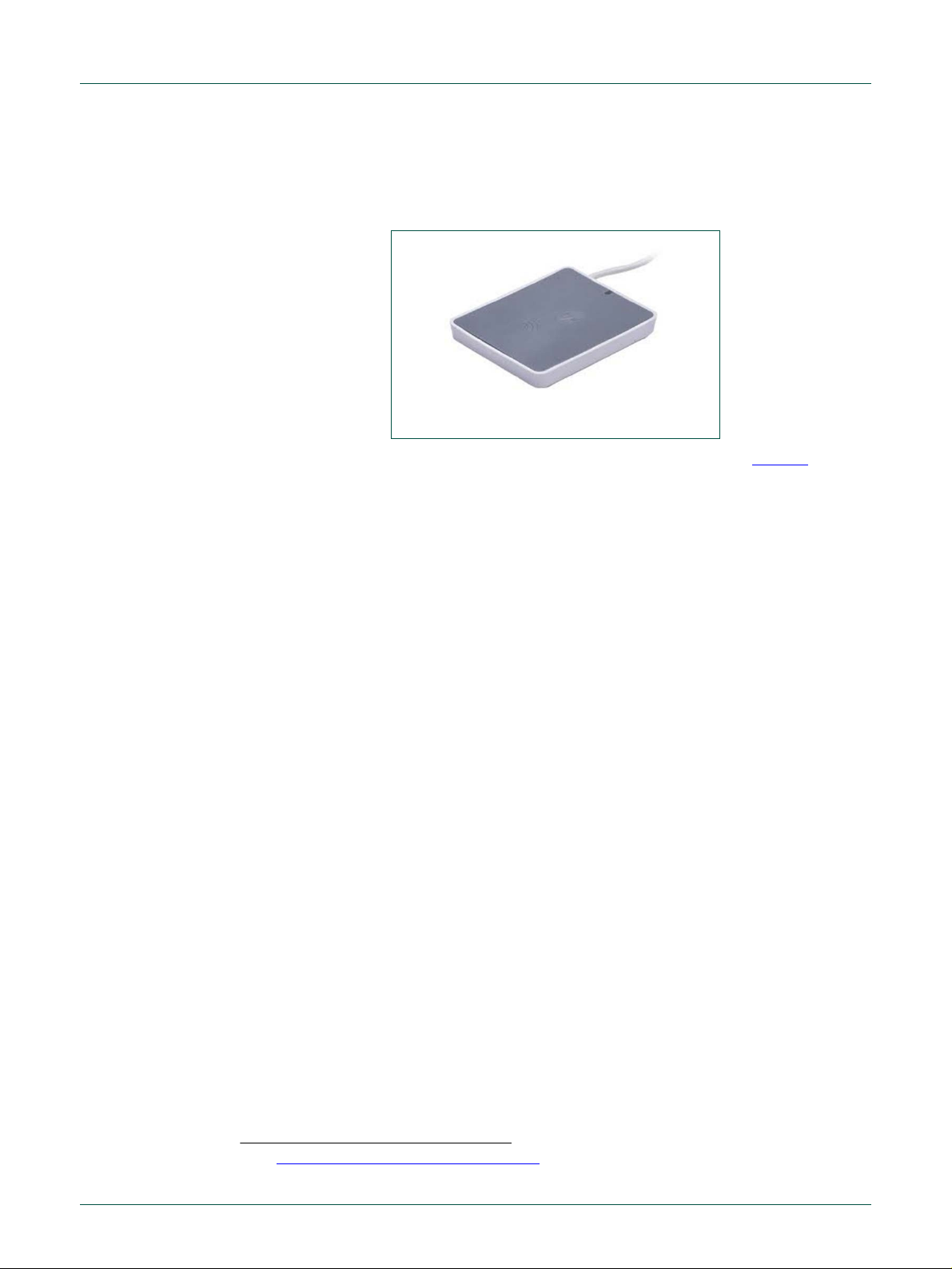
Fig 5. Identiv uTrust CLOUD 3700F reader
3.1.4 USB reader
Instead of a NFC dev ice, the USB (PCSC) reader (Identiv uT r us t CLO UD 37 00F ) may be
used in combination with the Windows app to develop applications.
To install the reader , do wnload latest driv er fr om the web page (r efer to [Identiv]), extract
“Identiv uTrust Installer.zip” and install it with no reader connected.
In Windows 7 operativ e systems, when a sm artcard is placed over the reader there is
frequently an issue regarding the smartcard mini-drivers. Although a solution to this
problem is given in this section , more inf ormation can be found on the W indows Support
Webpage
Group Policy has to be changed to prim ary group policy settings for smart cards. The
procedure is as follows:
2
. To s olve t his is sue t he Sm art Card P lug has to be disabled and Play in local
1. Click Start, type gpedit.msc in the Search programs and files box, and then
press ENTER.
2. In the console tree under Computer Configuration, click Administrative
Templates.
3. In the details pane, double-click Windows Components, and then doubleclick Smart Card.
4. Right-click Turn on Smart Card Plug and Play service, and then click Edit.
5. Click Disabled, and then click OK.
6. Click Start, type regedit.exe in the Search programs and files box, and then
press ENTER.
7. Go through the tree key, on the left, up to the key
• HKEY_LOCAL_MACHINE \ Software \ Microsoft \ Cryptography \
Calais for 32-bit system or
• HKEY_LOCAL_MACHINE \ SOFTWARE \ Wow6432Node \ Microsoft \
Cryptography \ Calais for 64-bit system
8. Add a new DWORD value nam ed CardDisconnectPowerDo wnDelay and set its
value to 0.
9. Click Start, type services.msc in the Search programs and files box, and then
press ENTER.
10. Find the smart card service in the list, right-click and click Restart.
11. Now you may plug the reader
2
https://support.microsoft.com/en-us/kb/976832.
Page 8

SECURITY
STATUS
NXP Semiconductors
UM10966
NTAG I²C plus Explorer Kit - Android Demo
UM10966
All information provided in this docum ent is subject to legal disclaimers.
© NXP Semiconductors N.V. 2017. All rights reserved.
User manual
COMPANY PUBLIC
Rev. 2.1 — 09 March 2017
360121
8 of 55
3.1.4.1 USB Reader firmware update
In some cases, reader is not functioning properly with Windows “NTAG I²C plus Demo”
application. This is due to newer Reader´s firmware. In this case, it needs to be updated,
using patch tool
3
.
3.2 Software components
3.2.1 NT AG I2C plus Explorer board firmware
The firmware runs on the NTAG I2C plus Explor er boar d and is flashed dur ing produc tion
at the MCU which supports the demonstration functionality of the hardware. The
delivered NTAG I
• NTAG_I
bootloader application. It is flashed at on-chip memory address starting at
0x0000 0000 and it is the f irst application to be executed after the MCU boots.
This application has three functions:
2
C plus Explorer board firmware consists of three applications:
2
C_Explorer_Bootloader: This project implements the secondary
o Jump to the start memory of the user application.
o Enter into flashing mode functionality.
o Enter into USB mode (Peek and Poke).
• NTAG_I
Android / Windows demonstration applications. It is flashed at on-chip flash
memory starting at 0x0 000 4000 address and it is executed af ter the bootloader
jumps to the application start address.
• NTAG_I
the NTAG_I
application is provided to il lustrate the NFC flashing functionality and its binary
image is provided embedded by default into the Android app (see Section 4.5).
3.2.2 Android app
The demo applicat ion on an Andro id NFC phone ( “NFC m obile”) sho wcasing t he various
features of the NT AG I
from the public NXP website as well as at Google Play.
2
C_Explorer_Demo: This project implements the logic supporting the
2
C_Explorer_Blink: This is a sample proj ect that sets into blinking m ode
2
C Explorer board as soon as the RF field is detected. This
2
C plus. The NT AG I2C Demo application is available f o r download
3
http://www.nxp.com/demoboard/OM5569-NT322ER/documents/software/SW4044.zip
Page 9
SECURITY
STATUS
NXP Semiconductors
UM10966
NTAG I²C plus Explorer Kit - Android Demo
UM10966
All information provided in this docum ent is subject to legal disclaimers.
© NXP Semiconductors N.V. 2017. All rights reserved.
User manual
COMPANY PUBLIC
Rev. 2.1 — 09 March 2017
360121
9 of 55
Fig 6. Android app GUI
Note: The UM10989 (refer to [UM10989]) descr ibes in detail how to get started with the
development of Android Applications.
3.2.3 Windows app
Together with the US B reader, the W indows app can be utilized to substitute a m issing
NFC mobile phone. The Windows app has similar functionaliti es as the An dr oi d a pp. This
software component is available as a download from the public NXP website. The
software will inclu de a setup file whic h will install the Windows App in the f o lder ‘Program
files/NXP Semiconduc tors’, this instal latio n proc ess will c reat e a sh ortc ut to t he W indo ws
App on your desktop. No further procedure is required to run this application.
1. Download the NTAG I
2. If not done, install the Identiv uTrust driver as described above and the NTAG I2C
Demo App
3. Launch the NTAG I
There are some po ints to consider when using the Windows App, since it is conn ec ted to
an external reader via USB. There are sometimes issues with the co nnection between
the reader and the tag. On these cas es, it is recommended to restart t he a pp and re-plug
the reader.
2
C Demo App (refer to [PC App])
2
C Demo App
Page 10
SECURITY
STATUS
NXP Semiconductors
UM10966
NTAG I²C plus Explorer Kit - Android Demo
UM10966
All information provided in this docum ent is subject to legal disclaimers.
© NXP Semiconductors N.V. 2017. All rights reserved.
User manual
COMPANY PUBLIC
Rev. 2.1 — 09 March 2017
360121
10 of 55
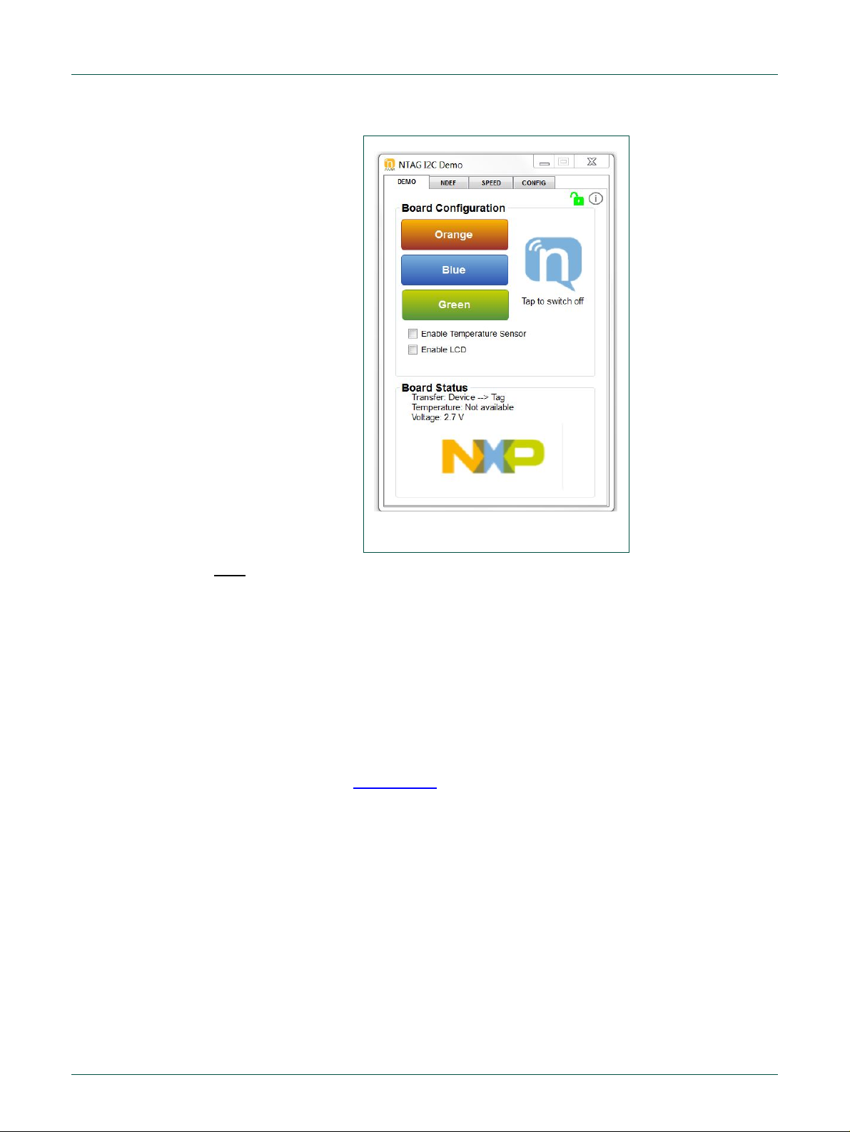
Fig 7. Windows application GUI
Note: The Windows application functionalities, GUI and look and feel are intentionally
made the sam e as the Android application . The Windows application is in ten ded t o run in
a Windows environment together with the Identiv uTrust CLOUD 3700F reader as a
substitute in case an NFC phon e is not available . Ther efore, this User Manual is valid f or
both the Android app and Windows applicat ion. However, only Android app screensho ts
are shown in this document.
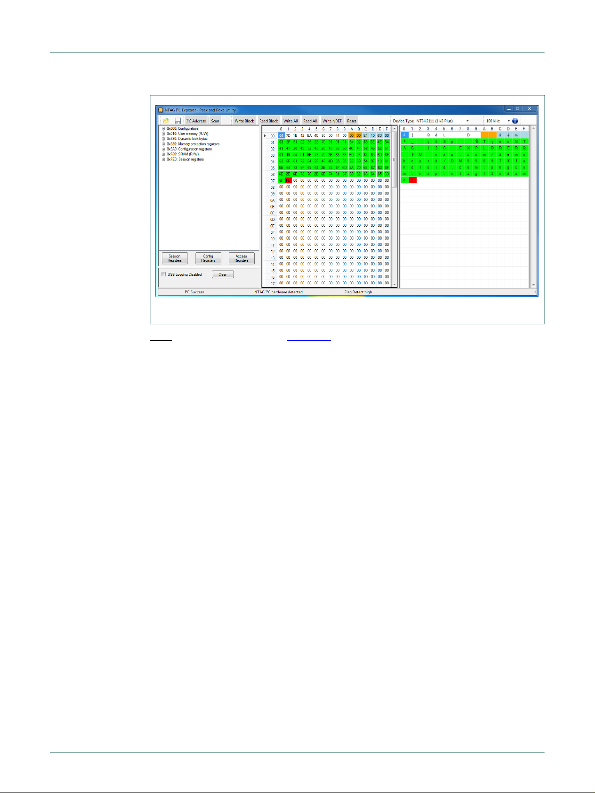
3.2.4 Peek and Poke GUI
The Peek and Poke GUI is a Windows app that can be used to examine the detailed
memory contents of the NT AG I
of view only a USB cab le connec tion fr om the b oard t o th e PC is neede d (n o ne ed of t he
USB NFC reader). This software component is available as a downlo ad from the public
NXP website (refer to [Peek&Poke]
.
2
C plus EEPROM via I2C interface. From hardwar e poi nt
).
Page 11
SECURITY
STATUS
NXP Semiconductors
UM10966
NTAG I²C plus Explorer Kit - Android Demo
UM10966
All information provided in this docum ent is subject to legal disclaimers.
© NXP Semiconductors N.V. 2017. All rights reserved.
User manual
COMPANY PUBLIC
Rev. 2.1 — 09 March 2017
360121
11 of 55
Fig 8. Peek and Poke GUI
Note: The UM10967 (refer to [ UM10967]) descr ibes in detail how to get started with the
Peek and Poke tool and the different functionalities it offers.
Page 12
SECURITY
STATUS
NXP Semiconductors
UM10966
NTAG I²C plus Explorer Kit - Android Demo
UM10966
All information provided in this docum ent is subject to legal disclaimers.
© NXP Semiconductors N.V. 2017. All rights reserved.
User manual
COMPANY PUBLIC
Rev. 2.1 — 09 March 2017
360121
12 of 55
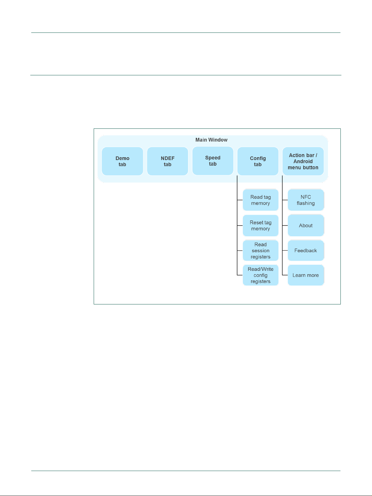
Fig 9. Application overview
4. NT AG I2C plus Explorer Demo app
The Android application is intended to operate on devices running Andr oid version 4.0
and above. The applicatio n has been optimized for a correct visioning of the graphical
elements in smartphones featuring different resolutions.
As seen in Fig 9, the Andr oid application consists of two demos that can be launched
from the main activity of the application and four configuration functionalities that are
accessed from the configuration selection view in the main activity.
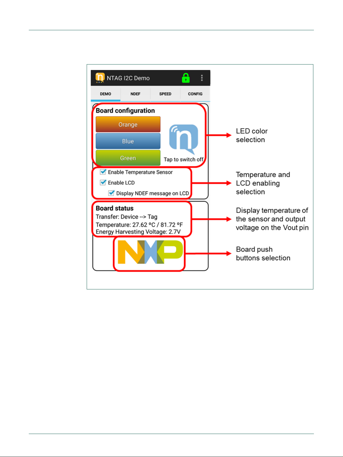
4.1 Demo tab
After the Splash wi ndo w c l os es, the Demo tab will a p pear. This screen allo ws th e us er to
launch the Demo tab itself, the NDEF demo tab, the Speed demo tab and access the
Configuration tab, with all configuration functionalities supported by the application.
Regarding the Demo tab, it allows demonstrating:
• The Energy harvesting functionality of the NTAG I
powering up of the complete dem o kit board with the energy harvested f rom the
RF interface without any battery.
• The RF to I
related color button on the NFC device screen.
• The I
the demo kit board reflected on the NFC device screen.
• The dynamic bidirectional communication between the two interfaces as the
temperature value as well as the voltage on the energy-harvesting pin get
dynamically updated on both the low power screen and the NFC device screen.
2
C com munication ena bling us to modify th e LED c olor b y pressing the
2
C to RF comm unication as the set of push buttons pres sed by the user o n
2
C plus that enables the
Page 13
SECURITY
STATUS
NXP Semiconductors
UM10966
NTAG I²C plus Explorer Kit - Android Demo
UM10966
All information provided in this docum ent is subject to legal disclaimers.
© NXP Semiconductors N.V. 2017. All rights reserved.
User manual
COMPANY PUBLIC
Rev. 2.1 — 09 March 2017
360121
13 of 55
Fig 10. Demo tab snapshot
Page 14
SECURITY
STATUS
NXP Semiconductors
UM10966
NTAG I²C plus Explorer Kit - Android Demo
UM10966
All information provided in this docum ent is subject to legal disclaimers.
© NXP Semiconductors N.V. 2017. All rights reserved.
User manual
COMPANY PUBLIC
Rev. 2.1 — 09 March 2017
360121
14 of 55
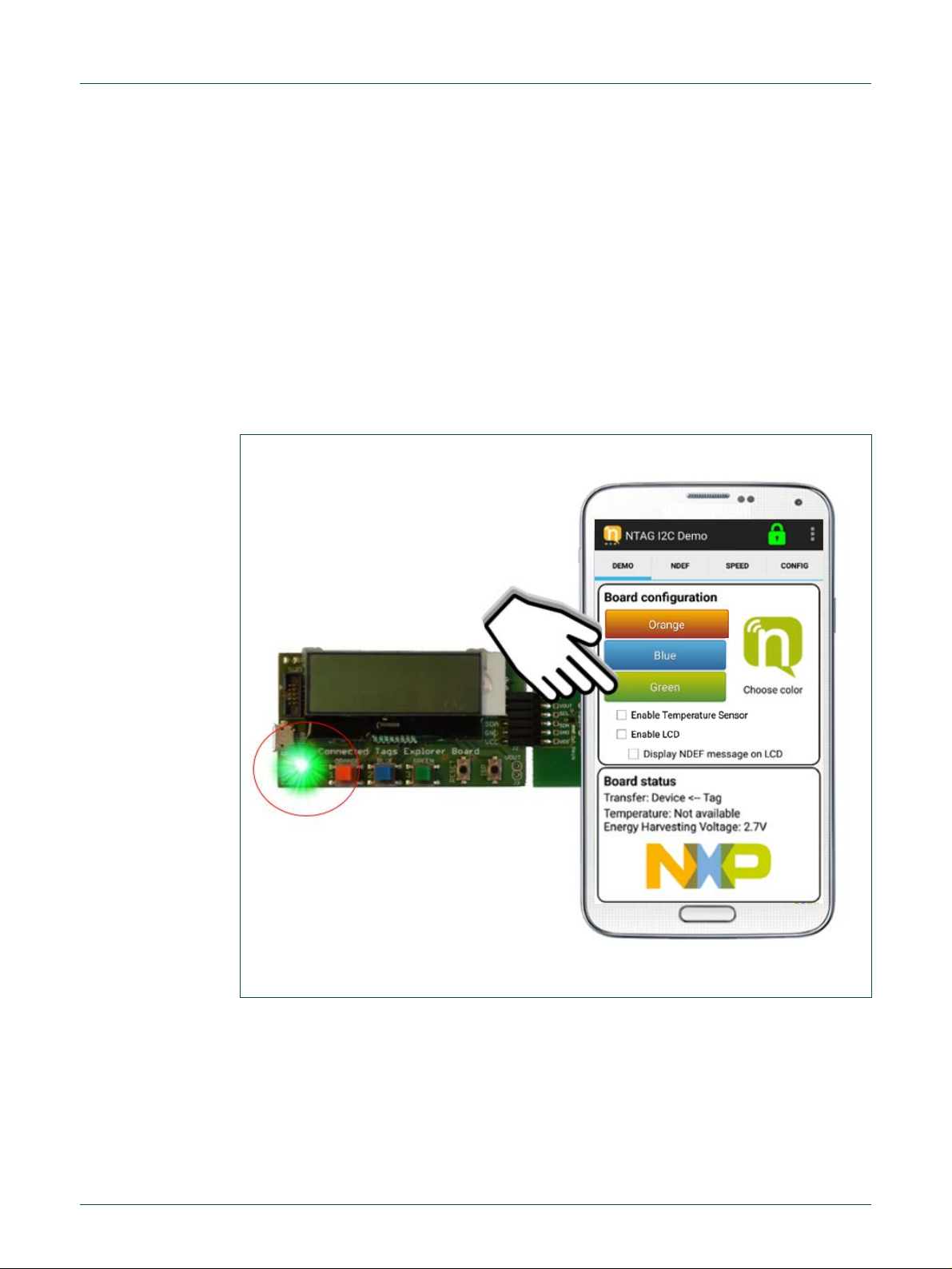
Fig 11. Green LED board configuration selection
4.1.1 Configuring NEK board to demonstrate RF to I2C communication
The board configuration p art of the demonstration s hows ho w the NTAG I2C plus passes
a command from the RF input throug h the SRAM and I
microprocessor, which acts upon the command and lights the appropriate LED.
1. Touch one of the colored board conf ig uration buttons on your mobile device. The
NTAG icon then changes color, indicating the color selection.
2. Tap your mobile device on the antenna. When properly placed, the LED will
illuminate in the chosen color. Optionally, the LCD display will display the
harvested voltage, the t emperature sensed by the board, the d efault text or the
stored NDEF message if the corresponding options are enabled in the board
configuration menu.
2
C serial interface outp ut to the
Page 15
SECURITY
STATUS
NXP Semiconductors
UM10966
NTAG I²C plus Explorer Kit - Android Demo
UM10966
All information provided in this docum ent is subject to legal disclaimers.
© NXP Semiconductors N.V. 2017. All rights reserved.
User manual
COMPANY PUBLIC
Rev. 2.1 — 09 March 2017
360121
15 of 55
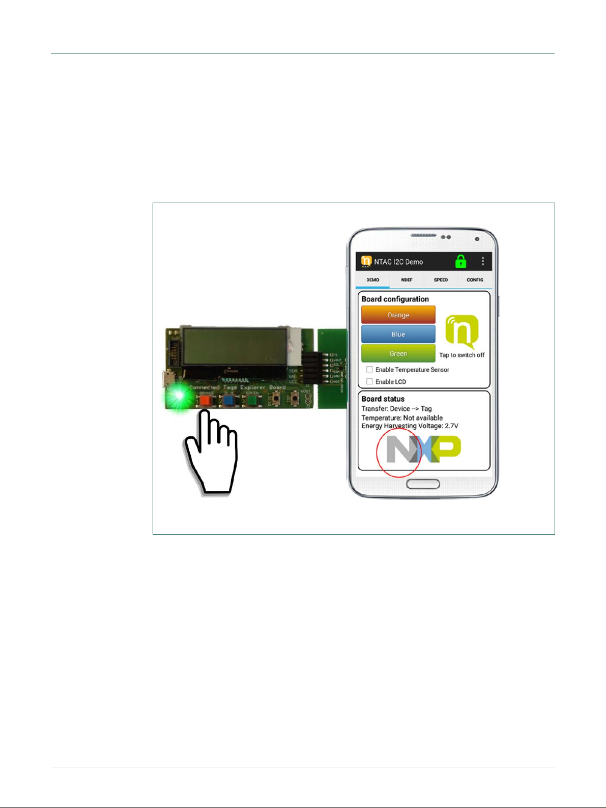
Fig 12. Reading board input
4.1.2 Reading board input to demonstrate I2C to RF communication
The three colored buttons on the NEK board demonstrate information from the board
beings transferred f rom the microprocessor through t he I
plus, which then sends it vi a the RF field t o the m obile devic e for dis pla y. W hen press ed,
each colored button on t he NEK boar d wi ll caus e a cor r espond ing s h ade of f on t he board
input NXP logo.
2
C serial bus to the N TAG I2C
Page 16
SECURITY
STATUS
NXP Semiconductors
UM10966
NTAG I²C plus Explorer Kit - Android Demo
UM10966
All information provided in this docum ent is subject to legal disclaimers.
© NXP Semiconductors N.V. 2017. All rights reserved.
User manual
COMPANY PUBLIC
Rev. 2.1 — 09 March 2017
360121
16 of 55
Fig 13. Temperature sensor demonstrates SRAM pass through mode
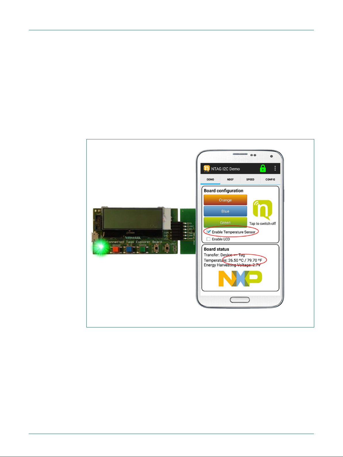
4.1.3 Temperature sensor
The NEK board incorporates a temperature sensor for measuring the ambient
temperature. This information can be shown in the Demo tab of the Android/PC
application. Addit ion all y it can be shown in the LCD displa y if the opt io n is c heck ed in the
menu.
This operation demonstrates the NTAG I
which data passes through its SRAM. It is also an other demonstration of passing data
from the microproc essor through the I
read through the RF interface for display on the mobile device.
2
C plus operating in pass-through mode, in
2
C serial bus to the NT AG I2C plus, which can be
Page 17
SECURITY
STATUS
NXP Semiconductors
UM10966
NTAG I²C plus Explorer Kit - Android Demo
UM10966
All information provided in this docum ent is subject to legal disclaimers.
© NXP Semiconductors N.V. 2017. All rights reserved.
User manual
COMPANY PUBLIC
Rev. 2.1 — 09 March 2017
360121
17 of 55
Fig 14. Enabling NEK board LCD
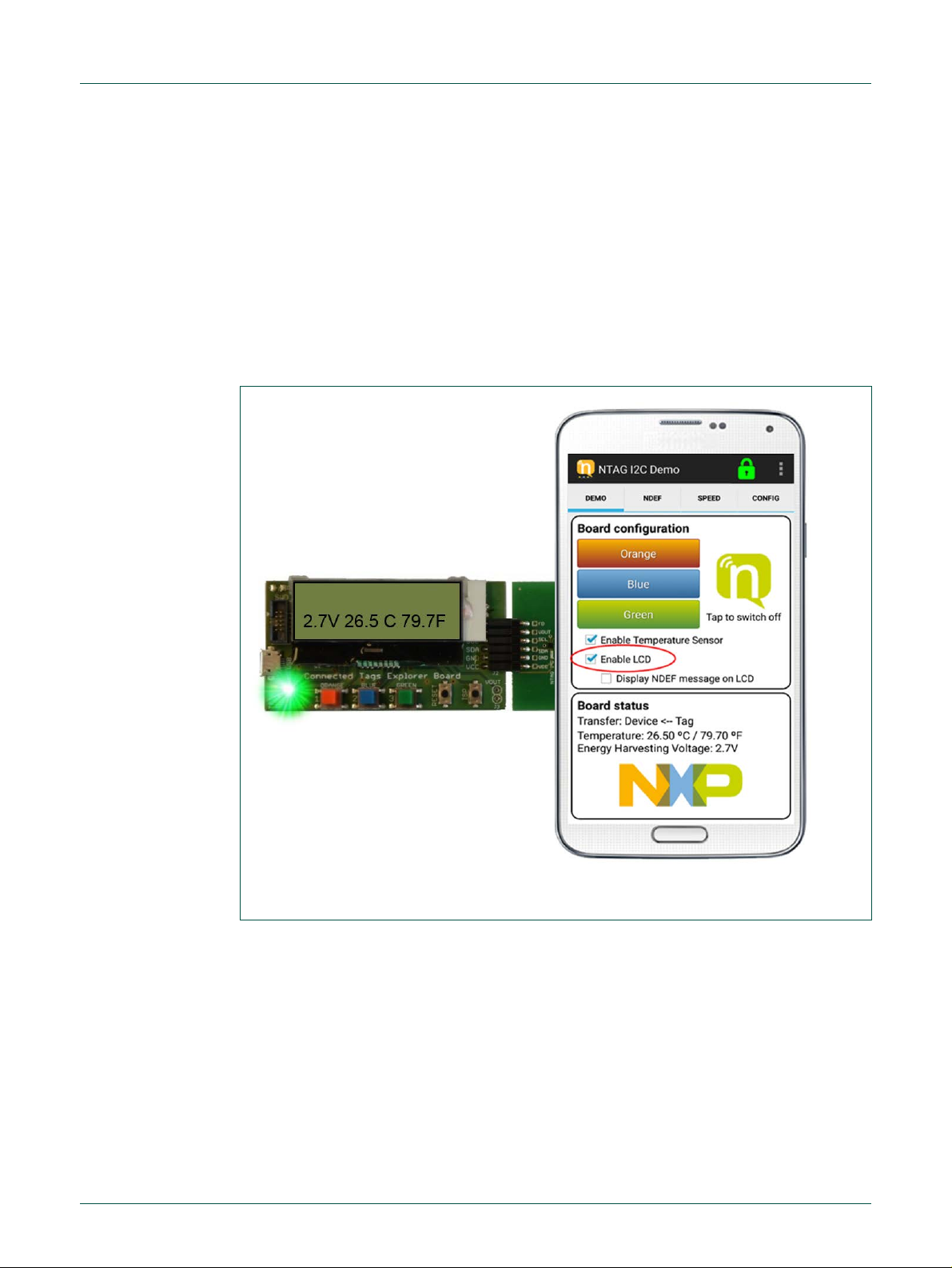
4.1.4 Enabling LCD display
You can enable th e NEK board LCD b y touching the Enable LCD se lection bo x. When
doing so, the LCD will show the predefined NTAG I
energy harvested and , if enabled, the temperature s ensed by the board in Celsi us and
Fahrenheit degrees.
Once again, this operation demonstrates the NTAG I
through mode sends a command from the RF input through the I
to the microprocessor, which in turn acts upon the command and turns on the LCD
display.
2
C plus Explorer text message, the
2
C plus chip operating in pass-
2
C serial interface output
Page 18

SECURITY
STATUS
NXP Semiconductors
UM10966
NTAG I²C plus Explorer Kit - Android Demo
UM10966
All information provided in this docum ent is subject to legal disclaimers.
© NXP Semiconductors N.V. 2017. All rights reserved.
User manual
COMPANY PUBLIC
Rev. 2.1 — 09 March 2017
360121
18 of 55
Fig 15. Displaying NDEF text message on NEK board LCD
4.1.5 Displaying NDEF text message on the NEK board LCD
You can displa y the ND EF text m ess age on the NEK boar d LCD b y touch ing the Display
NDEF message on LCD selection box.
Again, this operation dem onstrates the NT AG I
First, the NDEF message is read from the NTAG I
transferred to the MCU using the SRAM memory, which displays it in the display.
2
C plus operating in pass-through mode.
2
C plus EEPROM memory and is
Page 19

SECURITY
STATUS
NXP Semiconductors
UM10966
NTAG I²C plus Explorer Kit - Android Demo
UM10966
All information provided in this docum ent is subject to legal disclaimers.
© NXP Semiconductors N.V. 2017. All rights reserved.
User manual
COMPANY PUBLIC
Rev. 2.1 — 09 March 2017
360121
19 of 55
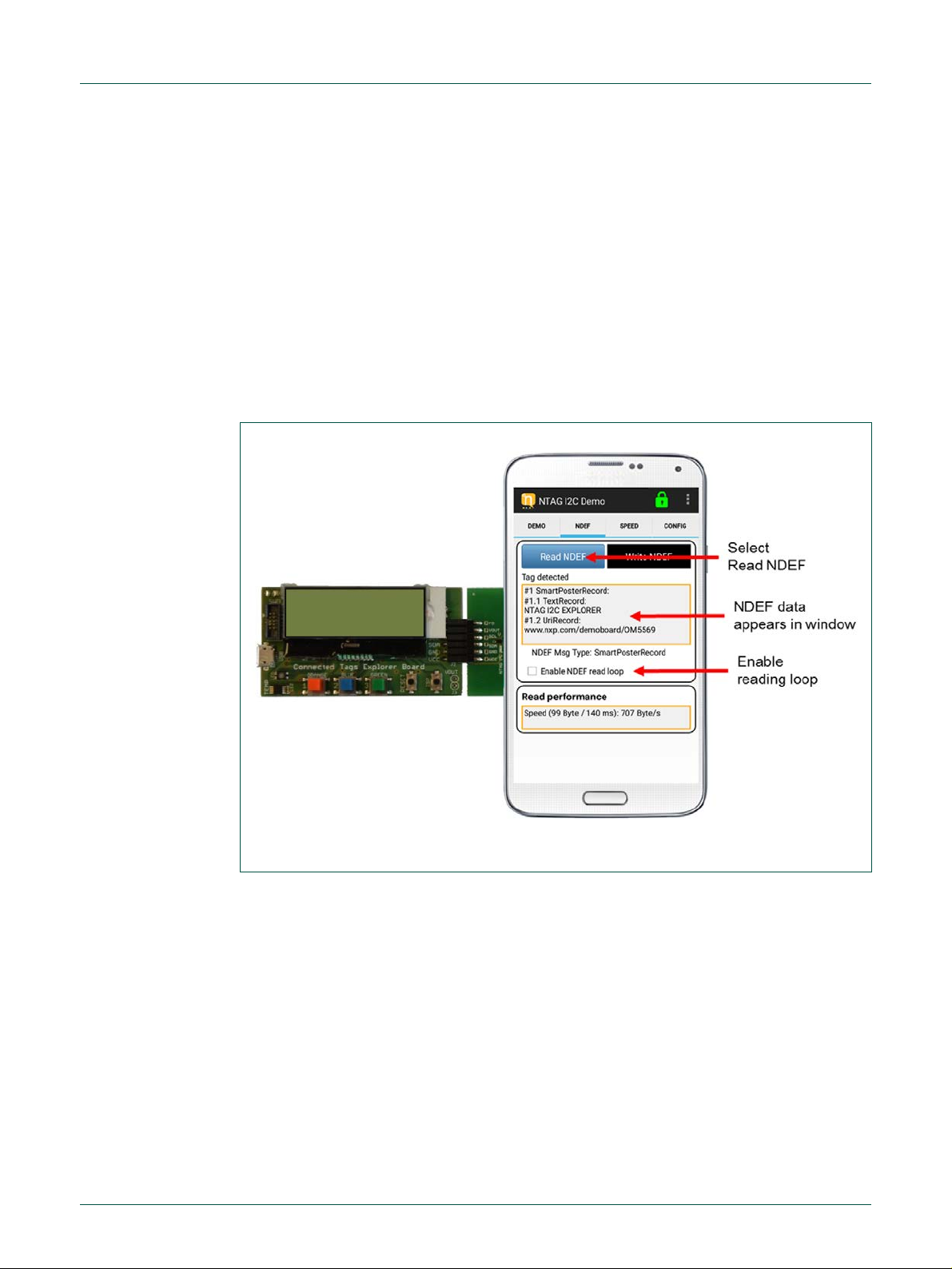
4.2 NDEF tab
The NDEF tab allows the user to r ead or write an NDEF m essage to the NT AG I2C plus
EEPROM. Actually, it could be used to read or write an NDEF message to any NFC
Forum Type 2 Tag, such as a MIFARE Ultralight, NTAG21x, ...
On the Read NDEF m ode, the ap pl ic ati on rea ds the NDEF message TLV from the NTAG
2
I
C plus and returns its content and the type of NDEF message.
On the Write NDEF m ode, the ap plicat ion allows th e user to write a T ext type, U RI type,
Bluetooth pairing type or Smart Poster NDEF message.
• Text record type is used to store plain text data.
• URI record type allows NFC tags to trigg er actions on the NFC de vice (usua lly the
smartphone), such as opening a webpage or sending an SMS message.
• Bluetooth pairing NDEF messages contain information about a Bluetooth device
that allows the smar tphone to pair with that Bluetooth device by just ta pping the
tag. In the case of writing a Bluetooth pairing type message, it is important to
remember that the MAC addr ess shall be 6 bytes, in hex adecimal (therefor e, 12
characters from 0 to F).
• Smart Poster record type defines a structure including a URI record type and a
Text record type as building blocks.
The NDEF tab also co nt a ins a Writ e def ault NDEF message button. When this butto n is
pressed, the application automatically writes a NDEF Smart Poster mes sage with the 2
records (optionally 3):
• Text record “NTAG I2C plus EXPLORER”
• URI content: www.nxp.com/demoboard/OM5569
.
• Optionally: AAR (Android Application Record)
More on Write default NDEF message is described below in section 4.2.2
.
Page 20

SECURITY
STATUS
NXP Semiconductors
UM10966
NTAG I²C plus Explorer Kit - Android Demo
UM10966
All information provided in this docum ent is subject to legal disclaimers.
© NXP Semiconductors N.V. 2017. All rights reserved.
User manual
COMPANY PUBLIC
Rev. 2.1 — 09 March 2017
360121
20 of 55
Fig 16. NDEF tab snapshot
When the NDEF message has been successfully written the “write tag successfully done”
popup appears temporarily in the application informing the user that t he message has
been correctly written. There is n o need to tap th e tag again if you want to write m ultiple
NDEF messages and read them in between.
In order to learn mor e about the different t ypes of NDEF mess ages and what structure
they have, please refer to the following NFC Forum specifications:
“NFC Data Exchange Format (NDEF) Technical Specifications”
“NFC Record Type Definition (RTD) Technical Specification”
“NFC Text RTD Technical Specification”
“NFC URI RTD Technical Specificati on”
“NFC Forum Connection Handover Technical Specification”
“NFC Smart Poster RTD Technical Specification”
“Bluetooth Secure Simple Pair ing Usin g NFC”
Page 21
SECURITY
STATUS
NXP Semiconductors
UM10966
NTAG I²C plus Explorer Kit - Android Demo
UM10966
All information provided in this docum ent is subject to legal disclaimers.
© NXP Semiconductors N.V. 2017. All rights reserved.
User manual
COMPANY PUBLIC
Rev. 2.1 — 09 March 2017
360121
21 of 55
Fig 17. Reading NDEF message stored in EEPROM of NTAG I2C plus
4.2.1 Reading NDEF data
To read a NDEF message out of NTAG I2C plus:
1. Select Read NDEF from the tab on the right of the mobile device screen.
2. Tap the mobile device onto the antenna.
3. A proper read will result in a m essage on the m obile device in dicating Read tag
successfully done. If no NDEF message is found or NTAG I²C plus is not
formatted as defined in NF C Forum Type 2 Tag s pec, it will result in a m essage
NTAG I2C plus product is not NDEF formatted. Additional ly, the Enable NDEF
read loop selec tion box can be used to se t the application to perm anently read
the EEPROM memory, so any change will automatically appear in the window.
Page 22
SECURITY
STATUS
NXP Semiconductors
UM10966
NTAG I²C plus Explorer Kit - Android Demo
UM10966
All information provided in this docum ent is subject to legal disclaimers.
© NXP Semiconductors N.V. 2017. All rights reserved.
User manual
COMPANY PUBLIC
Rev. 2.1 — 09 March 2017
360121
22 of 55
Fig 18. Writing NDEF message to NTAG I2C plus EEPROM
4.2.2 Writing NDEF data
To write an NDEF message into the NTAG I2C plus:
1. Select Write NDEF from the tab on the right of the mobile device screen.
2. Type a message into the NDEF message area. Or alternatively, press Write
Default NDEF message on your screen, which writes a NDEF Smart Poster
message with the text content: “NTAG I2C plus EXPLORER” and the URI
content: www.nxp.com/demoboard/OM5569
NDEF message an Android Applicatio n Record (AAR) , which adds the p ackage
name of the NTAG I
record. You can add an AAR to any NDEF record of your NDEF message
because Android searches the entire NDEF message for AARs. If it finds an
AAR, it starts the applicati on based on the pack age name inside the AAR. If the
application is not pr esent on the device, Google Pla y is launched to do wnload
the application.
. Additionally, you can add to your
2
C plus Demo application embedded inside the NDEF
3. Tap the mobile device onto the antenna.
4. A proper write will result in a mes sage on the mobile device indicating write tag
successfully done.
Page 23
SECURITY
STATUS
NXP Semiconductors
UM10966
NTAG I²C plus Explorer Kit - Android Demo
UM10966
All information provided in this docum ent is subject to legal disclaimers.
© NXP Semiconductors N.V. 2017. All rights reserved.
User manual
COMPANY PUBLIC
Rev. 2.1 — 09 March 2017
360121
23 of 55
Fig 19. Data transfer speed measurement concept behind the SRAM selection
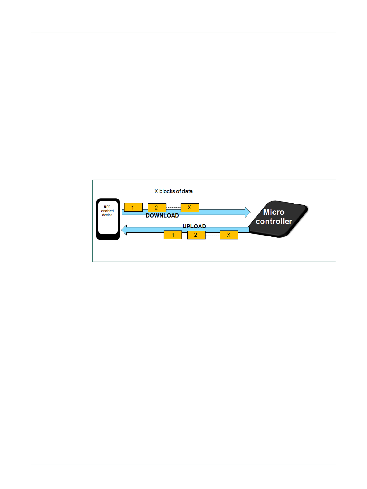
4.3 Speed tab
The speed Test Demo measures the transfer bit rate when communicating with the
NTAG I
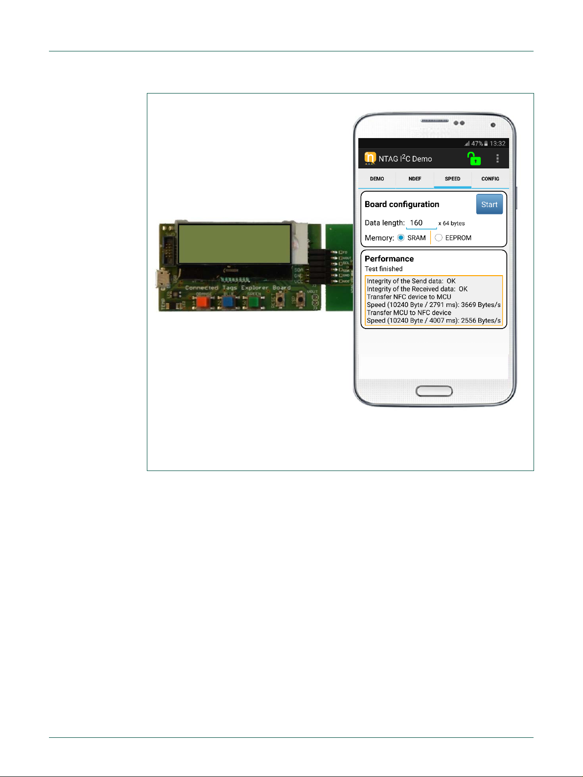
4.3.1 SRAM speed test
The SRAM speed Test measures the speed at which the data is transferred from the
application to the microcontroller through the SRAM (with the NTAG I
through mode), and vice versa. First, the application writes data to the SRAM several
times, and the microcontroller reads from it. This way, the throughput of the
communication in pass-through m ode from the application to the microcontroller can be
obtained. Once this f irst test has finished, the m icrocontroller starts writing to the SRAM
memory, while the application reads from it. This way, the throughput from the
microcontroller to the application can be measured.
2
C plus Explorer board according to different configurations.
2
C plus in pass-
Since the s ize of the SR AM m emory is 64 bytes, the data to be transm itted and rec eived
has to be a multiple of 64. Actually, what is transmitted is the number of 64-byte block s
defined by the user in the Block multiplier field (10 by default).
The integrity of the d ata trans fer red in both dir ections is c heck ed b y appending a C RC32
value in the last b lock. The CRC32 is calculated f or the whole message that h as been
transferred (for all the blocks). If the CRC32 from the message received by the
application is right, it will show an “Integrity of the data: OK” message. On the other hand,
if the CRC32 from the m essage received by the board is right, it will turn on the green
LED at the end of the Speed Test.
Once the test has been finished, both the application and the microcontroller indicate
whether the integrit y check was succ essful ( through a green LED at th e m icrocontrol ler),
and the application shows the time, mean speed and data transferred for both directions.
Page 24
SECURITY
STATUS
NXP Semiconductors
UM10966
NTAG I²C plus Explorer Kit - Android Demo
UM10966
All information provided in this docum ent is subject to legal disclaimers.
© NXP Semiconductors N.V. 2017. All rights reserved.
User manual
COMPANY PUBLIC
Rev. 2.1 — 09 March 2017
360121
24 of 55
Fig 20. SRAM Speed test snapshot
Page 25
SECURITY
STATUS
NXP Semiconductors
UM10966
NTAG I²C plus Explorer Kit - Android Demo
UM10966
All information provided in this docum ent is subject to legal disclaimers.
© NXP Semiconductors N.V. 2017. All rights reserved.
User manual
COMPANY PUBLIC
Rev. 2.1 — 09 March 2017
360121
25 of 55
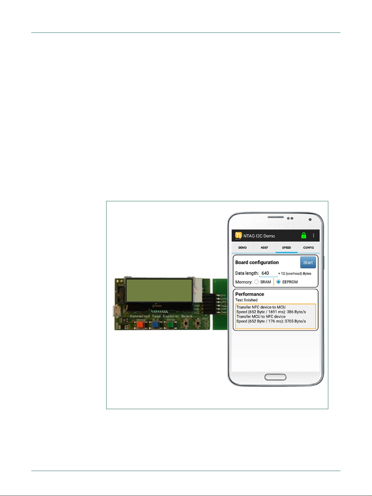
Fig 21. EEPROM Speed test snapshot
4.3.2 EEPROM speed test
The EEPROM Speed Test measur es the speed at which the applicat ion is able to write
and read the EEPROM memory of the NTAG I
message is written to t he EEPROM, and then, the same NDEF m essage is read. The
written NDEF mess age is a tex t t ype message that contains th e da ta i n the textbox of the
application repeated as many times as indicated in the Block multiplier field.
First, the applicatio n creates the NDEF mess age to be written by creating a string that
contains the content from the textbox as many times as indicated, and adding the
appropriate header. T hen, it writes it to the EEPROM m emory by sendin g as man y NFC
Forum T ype 2 Tag Write comm ands as neces sar y, and m easuring t he tim e it ta k es to do
so. Once it has finished writing, it reads the NDEF message from the NTAG I
EEPROM memory.
Once the test is f inished, the application s hows the number of b ytes, mean speed and
time for both the readi ng and writin g proces s. T he user c an also check the cont ent of the
memory to ensure that the NDEF message has been written appropriately.
2
C plus. In order to do this, an NDEF
2
C plus
Comparison between EEPROM read/write Fig 21 and SRAM read/write Fig 20 is
represented. Performing operations on SRAM memory with FAST_READ and
FAST_WRITE commands, highly improve overall communication speed.
Page 26

SECURITY
STATUS
NXP Semiconductors
UM10966
NTAG I²C plus Explorer Kit - Android Demo
UM10966
All information provided in this docum ent is subject to legal disclaimers.
© NXP Semiconductors N.V. 2017. All rights reserved.
User manual
COMPANY PUBLIC
Rev. 2.1 — 09 March 2017
360121
26 of 55
Fig 22. CONFIG tab menu
4.4 Configuration tab
This tab shows a selection menu that provides access to the different configuration
activities of the NT AG I
may select Read Tag Memory, Reset Tag Memory, Read Session Registers or
Read/Write Configuration registers.
2
C plus supported by the application. Fr om this screen, the user
Page 27
SECURITY
STATUS
NXP Semiconductors
UM10966
NTAG I²C plus Explorer Kit - Android Demo
UM10966
All information provided in this docum ent is subject to legal disclaimers.
© NXP Semiconductors N.V. 2017. All rights reserved.
User manual
COMPANY PUBLIC
Rev. 2.1 — 09 March 2017
360121
27 of 55
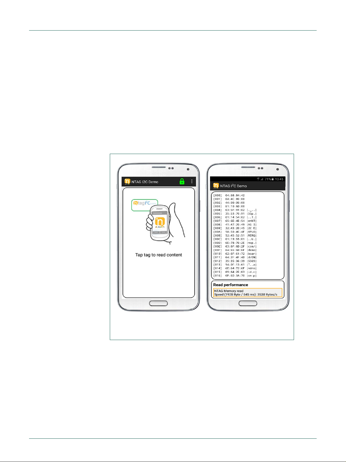
Fig 23. Read tag memory snapshot
4.4.1 Reading tag memory
This option reads and displays on the screen the content of the whole memory of the
NTAG I
tag memory:
For security reasons, the pages from 0xE2 to 0xFF in the sector 0 are hidden when
reading all the memory. These bytes define the PWD, PACK, AUTH0, PT_I2C and
ACCESS bytes.
2
C plus product. T h e c omplete content can be sc r olled on t he s c r een. T o read the
1. Select Read Tag Memory from the Configuration tab.
2. Tap the mobile device to the antenna (it might take 2-3 seconds to read the
memory content.
3. The screen will display the entire memory contents.
Page 28
SECURITY
STATUS
NXP Semiconductors
UM10966
NTAG I²C plus Explorer Kit - Android Demo
UM10966
All information provided in this docum ent is subject to legal disclaimers.
© NXP Semiconductors N.V. 2017. All rights reserved.
User manual
COMPANY PUBLIC
Rev. 2.1 — 09 March 2017
360121
28 of 55
Fig 24. Reset tag snapshot
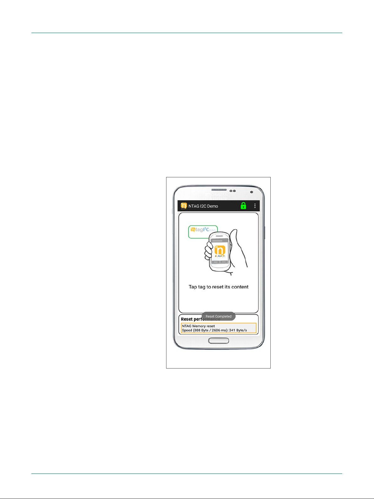
4.4.2 Resetting tag memory
This configuration functionality is about resetting the whole user memory of the NTAG I2C
plus product to the original content that was programmed during production.
1. Select Reset Tag memory from the Config tab screen.
2. Tap the mobile device to the antenna tag. The user should tap the NTAG I
plus device for 2-3 seconds to reset the memory content.
3. Upon successful reset, a banner indicating completion will be displayed along
the bottom of the screen.
In addition, when the user runs the reset mem ory on the NTAG I
write the PWD to 0xF FF FF FF F, AU T H0 to 0x F F, P AC K to 0x 000 0, A CC E SS to 0x00 and
PT_I2C to 0x00. These are the default values for the access configuration.
2
C PLU S version, it will
2
C
Alternatively, we can a lso reset the tag contents if we k eep the second button pressed
and tap the p hone with the NF C communication e nabled. W hen the LED is set to green,
the tag memory has been reset to the default NDEF SmartPoster.
Page 29

SECURITY
STATUS
NXP Semiconductors
UM10966
NTAG I²C plus Explorer Kit - Android Demo
UM10966
All information provided in this docum ent is subject to legal disclaimers.
© NXP Semiconductors N.V. 2017. All rights reserved.
User manual
COMPANY PUBLIC
Rev. 2.1 — 09 March 2017
360121
29 of 55
Fig 25. Alternative way to reset tag
Page 30

SECURITY
STATUS
NXP Semiconductors
UM10966
NTAG I²C plus Explorer Kit - Android Demo
UM10966
All information provided in this docum ent is subject to legal disclaimers.
© NXP Semiconductors N.V. 2017. All rights reserved.
User manual
COMPANY PUBLIC
Rev. 2.1 — 09 March 2017
360121
30 of 55
Fig 26. Read Session registers snapshot
4.4.3 Reading session registers
This option displa ys the content of the session registers in the NTAG I2C plus. Session
registers are used to configure or monitor the registers values of the current
communication session. Session registers values can be modified within a particular
communication sess ion ( on l y v ia t he I
them). However, after Power-On-Reset, these values go back to their default
configuration values, which are obtained from the configuration registers.
2
C interface, so the a ppl ication is not able to modify
Session registers values c a n be r ea d on pages F8h to F 9h (s ec tor 3) vi a the RF int erf ac e
or at block FEh via the I
2
C interface.
To read the tag session registers:
1. Select Read Session Registers from the Config tab screen.
2. Tap the mobile device to the tag antenna.
3. Upon successful read, the session registers values will be shown. Tapping o n
any of the right-f acing arrows will bring up more details. A blue mark indicates
ON or selected.
Page 31

SECURITY
STATUS
NXP Semiconductors
UM10966
NTAG I²C plus Explorer Kit - Android Demo
UM10966
All information provided in this docum ent is subject to legal disclaimers.
© NXP Semiconductors N.V. 2017. All rights reserved.
User manual
COMPANY PUBLIC
Rev. 2.1 — 09 March 2017
360121
31 of 55
Session register values are displayed on the screen divided into different groups:
• General Chip Information: General information about the discovered NTAG I
plus product. It shows the following information:
o IC product: NTAG I
o User Memory: Size of the user memory of the NTAG I
• NTAG Configuration: General NTAG configuration:
2
o I
C RST on start is: Shows the content of the I2C_RST_ON_OFF bit,
which is responsible for enabling a soft reset through an I
start.
• Field Detection: Information related to the field detection functionality, which is
used for the smart pairing with devices, as it triggers a signal to the connec ted
host when the NTAG I
o FD_OFF: Shows the co ntent of the FD_OFF bits, which define th e event
upon which the signal output on the field detection pin is brought up.
2
C plus chip version.
2
C plus chip.
2
C repeated
2
C plus product is powered by an external NFC device.
2
C
o FD_ON: Shows the content of the FD_ON bits, which define the event
upon which the signal output on the field detection pin is brought down.
o Last NDEF Page is: Shows the content of the LA ST _N DEF_ BLO C K byte,
this is the address of the last block (I
NDEF message.
o NDEF Data Read is: Shows the content of the NDEF_DATA_READ bit.
o RF Field present is: S hows the co ntent of the RF_FIELD_PR ESENT bit,
which indicates if an RF field is detected.
• Pass through: Information related to the pas s-through functionality, which allo ws
the fast transfer of data between the R F and the I
SRAM memory.
o Pass Through is: Shows the content of the PT HRU_ON_OFF bit, which
is responsible for enabling the data transfer via the SRAM memory.
2
o I
C locked is: Shows th e content of the I2C_LOCKED bit, which can lock
the access to memory to the I
o RF locked is: Sho ws the content of the RF_LOCKED bit, which can lock
the access to memory to the RF interface.
o SRAM I
which indicates if the data in the SRAM memor y is ready to be read by
the I
o From RF to I
defines the data flow direction for the data transfer.
2
C ready is: Shows the content of the SRAM_I2C_READY bit,
2
C interface.
2
C is: Shows the content of the PTHRU_DIR bit, which
2
C interface.
2
C interface addressing) of the
2
C interface by usin g a 64 byte
• SRAM Memory settings: Information about the SRAM mirroring feature. The
SRAM memory can be mirrored in the User Memor y for RF access b y enabling
the SRAM mirroring feature.
o SRAM Mirror: Shows the content of the SRAM_MIRROR_ON_OFF bit.
o SRAM M irror block: Shows the conten t of the SRAM_MIRROR_BLOC K
byte, which indicates the address of the first block (I
addressing) of the mirror of SRAM memory.
2
C interface
Page 32

SECURITY
STATUS
NXP Semiconductors
UM10966
NTAG I²C plus Explorer Kit - Android Demo
UM10966
All information provided in this docum ent is subject to legal disclaimers.
© NXP Semiconductors N.V. 2017. All rights reserved.
User manual
COMPANY PUBLIC
Rev. 2.1 — 09 March 2017
360121
32 of 55
Fig 27. Read / Write configuration registers snapshot
• I2C Settings: Information about the I2C management configuration.
o WD_LS Ti mer is: Sho ws the conte nt of the W DT_LS byte: the LS B of the
watchdog time control register.
o WD_MS T imer: Shows the content of the W DT_MS byte: the MSB of the
watchdog time control register.
2
o I
C Clock stretch: Shows the content of the I2C_CLOCK_STR bit, which
is responsible for enabling the I
For further inform ation about the session registers b ytes, please refer to the NTAG I
plus product data sheet (refer to [NTAGI2Cplus
4.4.4 Reading / Writing configuration registers
Configuration register s define the def ault functi onalities of the NTAG I2C plus to be use d
for the communication after a Power-On-Reset.
2
C clock stretching.
]).
2
C
Configuration register s values can be read and written in Pages E8h and E9h ( sector 0
for NTAG I
selected by pressing the Read/Write config buttons on top of the window.
For further informat ion about the co nfiguration reg isters bytes, p lease consult t he NTAG
2
I
C plus product datasheet (refer to [NTAGI2Cplus]).
2
C plus 1k). The operation to be performed, read or write, in each tap is
Page 33

SECURITY
STATUS
NXP Semiconductors
UM10966
NTAG I²C plus Explorer Kit - Android Demo
UM10966
All information provided in this docum ent is subject to legal disclaimers.
© NXP Semiconductors N.V. 2017. All rights reserved.
User manual
COMPANY PUBLIC
Rev. 2.1 — 09 March 2017
360121
33 of 55
To read configuration registers:
1. Select Read/Write Config registers from the Config tab screen.
2. Tap the mobile device to the antenna tag.
3. Upon successful read, the configuration registers values will be shown.
4. To write the configurati on registers, s witch to W rite config. Register contents are
controlled either via dr opdown menus, direc t input or by slider contr ollers where
grey indicates OFF and blue indicates ON.
Configuration register values are displayed on the screen divided into different groups:
• General Chip Information: General information about the discovered NTAG I
plus product. It shows the following information
o IC product: NTAG I
o User Memory: Size of the user memory of the NTAG I
2
C plus chip version
2
C plus chip
2
C
• Field Detection: Information related to the field detection functionality, which is
used for the smart pairing with devices, as it triggers a signal to the connec ted
host when the NTAG I
o FD_OFF: Shows the co ntent of the FD_OFF bits, which define th e event
upon which the signal output on the field detection pin is brought up
o FD_ON: Shows the content of the FD_ON bits, which define the event
upon which the signal output on the field detection pin is brought down
• Pass through: Information related to the pas s-through functionalit y, which allows
the fast transfer of data between t he RF and the I
SRAM memory.
o Functionality: Shows the content of the PTHRU_ON_OFF bit, which is
responsible for enabling the data transfer via the SRAM memory.
o Direction: Shows the c ontent of the TRANSFER_DI R bit, which defines
the data flow direction for the data transfer.
o Write from RF: Shows the c ontent of the TRANSFER_D IR bit (same as
direction), which defines the data flow direction for the data transfer
• SRAM Memory settings: Information about the SRAM mirroring feature. The
SRAM memory can be mirrored in the User Memor y for RF access b y enabling
the SRAM mirroring feature.
o Last NDEF Page: Sh ows the content of the LAST_NDEF_ BLOCK byte,
this is the address of the last block (I
NDEF message.
2
C plus product is powered by an external NFC device.
2
C interface by using a 64 byte
2
C interface addressing) of the
o SRAM Mirror: Shows the content of the SRAM_MIRROR_ON_OFF bit.
o SRAM M irror block: Shows the conten t of the SRAM_MIRROR_BLOC K
• I2C Settings: Information about the I2C management configuration.
o WD_LS Timer: Sho ws the content of the W DT_LS byte: the LSB of the
byte, which indicates the address of the first block (I
addressing) of the mirror of SRAM memory.
watchdog time control register
2
C interface
Page 34

SECURITY
STATUS
NXP Semiconductors
UM10966
NTAG I²C plus Explorer Kit - Android Demo
UM10966
All information provided in this docum ent is subject to legal disclaimers.
© NXP Semiconductors N.V. 2017. All rights reserved.
User manual
COMPANY PUBLIC
Rev. 2.1 — 09 March 2017
360121
34 of 55
o WD_MS T imer: Shows the content of the W DT_MS byte: the MSB of the
watchdog time control register
2
o I
C Clock stretch: Shows the content of the I2C_CLOCK_STR bit, which
is responsible for enabling the I
2
C RST on start: Shows the c ontent of the I2C_RST_ON_OFF bit , which
o I
is responsible for enabling a soft reset through an I
• Access Configuration: Information about the I
o AUTH0: This is the first page of the Sec tor 0 where the authentication is
needed in order to acces s the user memory from NFC perspective. By
default the AUTH0 value is 0xFF, this means that the password
protection is effectively disabled. When the user introduces a new
password this AUTH0 will be automatically set to 0x03.
o NFC Prot: Sho ws t he memory protection b it. If s et to O FF onl y the wr ite t o
the protected area is protec ted by the password. If set to ON, read and
write into the protected area is protected by password.
2
C clock stretching.
2
C repeated start.
2
C management configuration.
o NFC DIS SEC 1: Shows the NFC access protection t o Sector 1. If set to
OFF the Sector 1 will be a ccessible in 2K vers ion. If set to ON, Sector 1
is not accessible and will return NACK0.
o AUTHLIM: Shows limitation of negative password authentication attempts.
If the limit is reached then the protected area will no longer be
accessible. Set to 0 means that limitation is disabled.
o 2K Prot: Shows the pass word protec tion for Sec tor 1 f or 2k version. If set
to OFF, t he pass word auth entication f or Sec tor 1 is disable d. Other wise,
if set to ON the password is needed to access to Sector 1.
o SRAM Prot: Shows the p assword protection for pass-through and mirr or
mode. If set to OFF th e password aut hentication f or pass-through m ode
is disabled. If set to ON then the password authentication to access
SRAM in pass-through is required.
o I2C Prot: Shows the acc ess to protected area from I
then the whole user m emory is accessible from I
the protected area is read only. Other value will disable the access to
protected area.
For further informat ion about the configurat ion register s bytes, please ref er to the NTAG
2
I
C plus product datasheet (refer to [NTAGI2Cplus]).
2
C perspective. If 0
2
C. If this value is 1 then
Page 35

SECURITY
STATUS
NXP Semiconductors
UM10966
NTAG I²C plus Explorer Kit - Android Demo
UM10966
All information provided in this docum ent is subject to legal disclaimers.
© NXP Semiconductors N.V. 2017. All rights reserved.
User manual
COMPANY PUBLIC
Rev. 2.1 — 09 March 2017
360121
35 of 55
Fig 28. Figure title here
Fig 29. LPC11U1x/2x flash sectors
4.5 Action bar
4.5.1 NFC Flashing via NTAG I2C plus Explorer demo
NTAG I2C plus enabl es data download cap ability. The on-chip SRAM permits tem porary
storage of data during the transfer, enabling the tag to act as a modem.
4.5.1.1 Design implementation choice
The NEK board em beds a LPC11U24. The following table shows th e correspondence
between sector numbers and memory addresses for LPC11U2x/1x devices.
Page 36

SECURITY
STATUS
NXP Semiconductors
UM10966
NTAG I²C plus Explorer Kit - Android Demo
UM10966
All information provided in this docum ent is subject to legal disclaimers.
© NXP Semiconductors N.V. 2017. All rights reserved.
User manual
COMPANY PUBLIC
Rev. 2.1 — 09 March 2017
360121
36 of 55
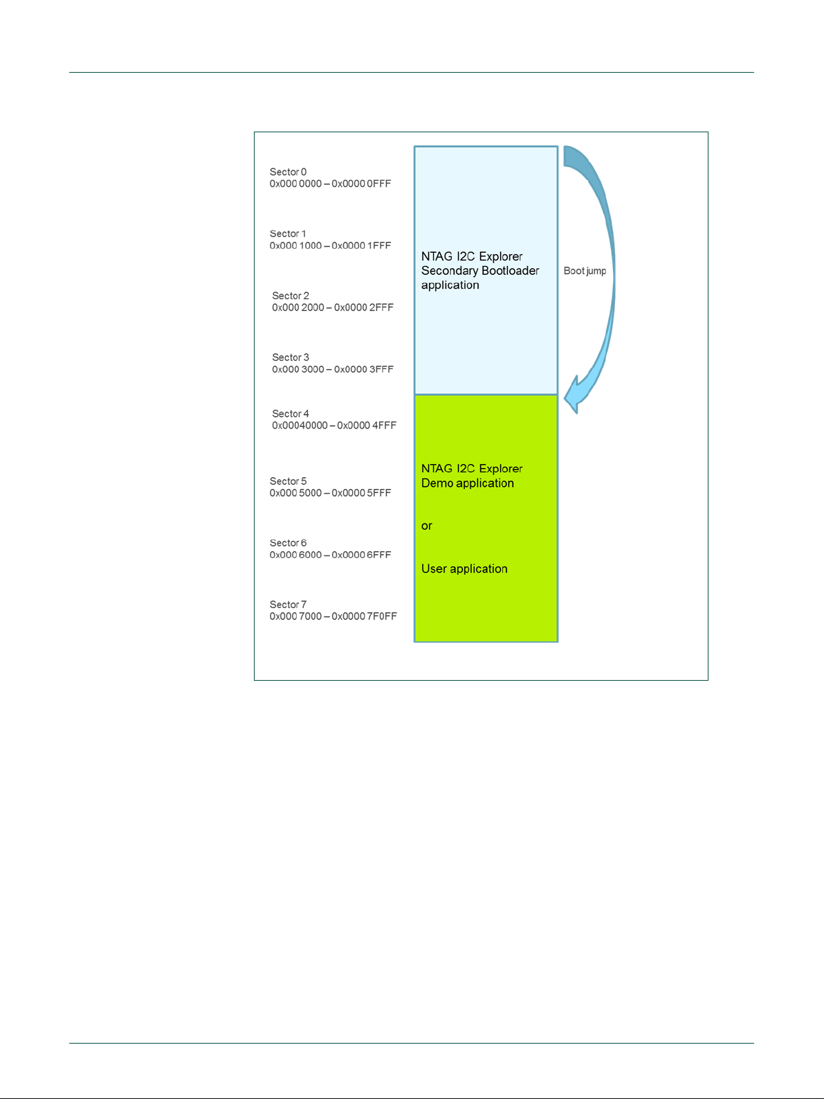
The on-chip flash mem ory of the LPC11U24 is grouped in s ectors. The flash mem ory is
divided into 8 sectors of 4 Kb each. Therefore, for LPC11 U24 we have 32Kb of Flash
memory available.
NXP’s LPC11U24 microcontroller provides two methods to update the flash contents:
• In-system-programming (ISP): We use this method when we flash new contents
using the USB port and a computer (drag-and-drop a binary file).
• In application programming (IAP): Programming is performed by erase and write
operation on the on-chip flash m emory, as directed by the end-user application
code this is the method we use for NFC flashing.
A secondary bootloader has been implemented in order to enable firmware flashing
through NFC inter face. A secondar y bootloader is a piece of code, which allows a user
application code to be downloaded via alternative channels to the USB (i.e.: NFC
flashing).
The primary bootloader is the firmware that resides in a microcontroller’s boot ROM block
and is executed on power -up and resets. After the b oot ROM’s executio n, the sec ondary
bootloader is executed. T he secondary bootlo ader in turn will then execut e the end-user
application.
Both the secondary boot loader and the us er appl icati on res ide in flas h. T herefor e, for the
secondary bo otloader to fla sh the user app licat ion w ithout m odif ying an y of its own c ode,
the user application should be flashed starting the next available sector.
Page 37
SECURITY
STATUS
NXP Semiconductors
UM10966
NTAG I²C plus Explorer Kit - Android Demo
UM10966
All information provided in this docum ent is subject to legal disclaimers.
© NXP Semiconductors N.V. 2017. All rights reserved.
User manual
COMPANY PUBLIC
Rev. 2.1 — 09 March 2017
360121
37 of 55
Fig 30. On-chip flash memory organization for NFC flashing functionality
The NEK secondary bootloader implements the IAP functionality that allows to
erase/write flash m emor y sectors dir ected b y the appl ic ation and t he HID dr ivers for USB
communication. In our case, the NEK secondary bootloader occupies 4 flash sectors.
This means that th is four f irst m emor y sectors are never er ased since they belong to the
secondary bootloader (they must always be there in order to have the NFC flashing
functionality available).
Therefore, we hav e 4 extra flash sectors available for end-user application (16 K b). In
this memory area, we store the NEK Demo (LED, Speed Tests, etc.), the blink
application or an y other us er appl ication. NFC f lashin g func tiona lity ac tuall y re-writes this
16 Kb with the user application send b y the Android or PC app via NFC interface. For
this reason, the maximum size of the binary file that can be upgraded through the
RF interface is 16 KB.
Page 38
SECURITY
STATUS
NXP Semiconductors
UM10966
NTAG I²C plus Explorer Kit - Android Demo
UM10966
All information provided in this docum ent is subject to legal disclaimers.
© NXP Semiconductors N.V. 2017. All rights reserved.
User manual
COMPANY PUBLIC
Rev. 2.1 — 09 March 2017
360121
38 of 55
Fig 31. NFC Flashing option selection within the Android app
4.5.1.2 How to flash new firmware through NFC
As an illustr ative exam ple, we are going to f lash the provided Blink application via NFC
flashing (green LED bl inks when detec ts th e pres e nc e of the R F f iel d) . Af ter this p r oces s ,
the default NTAG Explorer Demo will be replaced by the Blink application
Pre-condition:
(1) Install NTAG I
(2) Verity that NEK board firmware version is v3.4
Main flow:
(1) Tap on the Context menu button on your phone or in the app (depending on
which phone you are using)
(2) Select the NFC Flashing option in the Android app
2
C plus Demo Android application v1.7.4
(3) Once in the NF C Flashing m enu, we need to select the binar y file to be flashed
into the NEK board MCU. We have two options:
- Select the Blink application or Demo application embedded by default in the
Android app by clicking on “Select from Appl” button.
Page 39

SECURITY
STATUS
NXP Semiconductors
UM10966
NTAG I²C plus Explorer Kit - Android Demo
UM10966
All information provided in this docum ent is subject to legal disclaimers.
© NXP Semiconductors N.V. 2017. All rights reserved.
User manual
COMPANY PUBLIC
Rev. 2.1 — 09 March 2017
360121
39 of 55
Fig 32. Selection of binary file to be flashed into MCU memory
Page 40

SECURITY
STATUS
NXP Semiconductors
UM10966
NTAG I²C plus Explorer Kit - Android Demo
UM10966
All information provided in this docum ent is subject to legal disclaimers.
© NXP Semiconductors N.V. 2017. All rights reserved.
User manual
COMPANY PUBLIC
Rev. 2.1 — 09 March 2017
360121
40 of 55
Fig 33. Selection of binary file to be flashed into MCU memory (II)
Fig 34. Entering NFC Flashing mode
- Alternat ively, we can s elect fr om the phone mem ory a binary fi le by clicking on
the “Select from Storage” button.
(4) NFC Flash ing m ode is e nable d in th e N EK boar d b y pressing the third colored
button (right button) before power up. While keeping the button pressed, we
tap the NEK board into the phone NFC sweet spot.
Page 41

SECURITY
STATUS
NXP Semiconductors
UM10966
NTAG I²C plus Explorer Kit - Android Demo
UM10966
All information provided in this docum ent is subject to legal disclaimers.
© NXP Semiconductors N.V. 2017. All rights reserved.
User manual
COMPANY PUBLIC
Rev. 2.1 — 09 March 2017
360121
41 of 55
Fig 35. NFC Flashing progress bar
As soon as we tap the NEK board, the NFC flashing will start. O nce the NFC Flashing
process has started, we can release the right button. This process may take some
seconds, it is important to keep the phone steady until the NFC flashing process has
finished (as indicated by the progress bar and green blinking LED).
In this example, we flash the Blink application binary file into the MCU memory. For doing
so, we need to click on Select from Appl button and click on LED Blinker.
Page 42

SECURITY
STATUS
NXP Semiconductors
UM10966
NTAG I²C plus Explorer Kit - Android Demo
UM10966
All information provided in this docum ent is subject to legal disclaimers.
© NXP Semiconductors N.V. 2017. All rights reserved.
User manual
COMPANY PUBLIC
Rev. 2.1 — 09 March 2017
360121
42 of 55
Fig 36. NFC Flashing successful execution
(5) When the NFC Flashing process has finished, both the Android app and the NEK
board notifies it to the user. In the Android app, a message appears on the
bottom part of the scr een. The NEK board blink s the green LED thre e times and
displays “Flashing OK”.
(6) If the process has finished successfully, we can now check if the Blink
application is installed and has replaced the previous Demo app.
Page 43

SECURITY
STATUS
NXP Semiconductors
UM10966
NTAG I²C plus Explorer Kit - Android Demo
UM10966
All information provided in this docum ent is subject to legal disclaimers.
© NXP Semiconductors N.V. 2017. All rights reserved.
User manual
COMPANY PUBLIC
Rev. 2.1 — 09 March 2017
360121
43 of 55
Fig 37. LED Blinker NFC Flashing upgrade verification
(7) If the proc ess has not fin ished suc cess fully, (e.g. due to an RF f ield lost), we can
retry as many times as required. For that, we need to go back to Step 1 and
repeat the entire process. Note that, if the flashing process has not finished
successfully, the pre vious installed firmware ma y be not usable, and therefore,
we need to retry flashing a new firmware.
Page 44
SECURITY
STATUS
NXP Semiconductors
UM10966
NTAG I²C plus Explorer Kit - Android Demo
UM10966
All information provided in this docum ent is subject to legal disclaimers.
© NXP Semiconductors N.V. 2017. All rights reserved.
User manual
COMPANY PUBLIC
Rev. 2.1 — 09 March 2017
360121
44 of 55
Fig 38. About tab snapshot
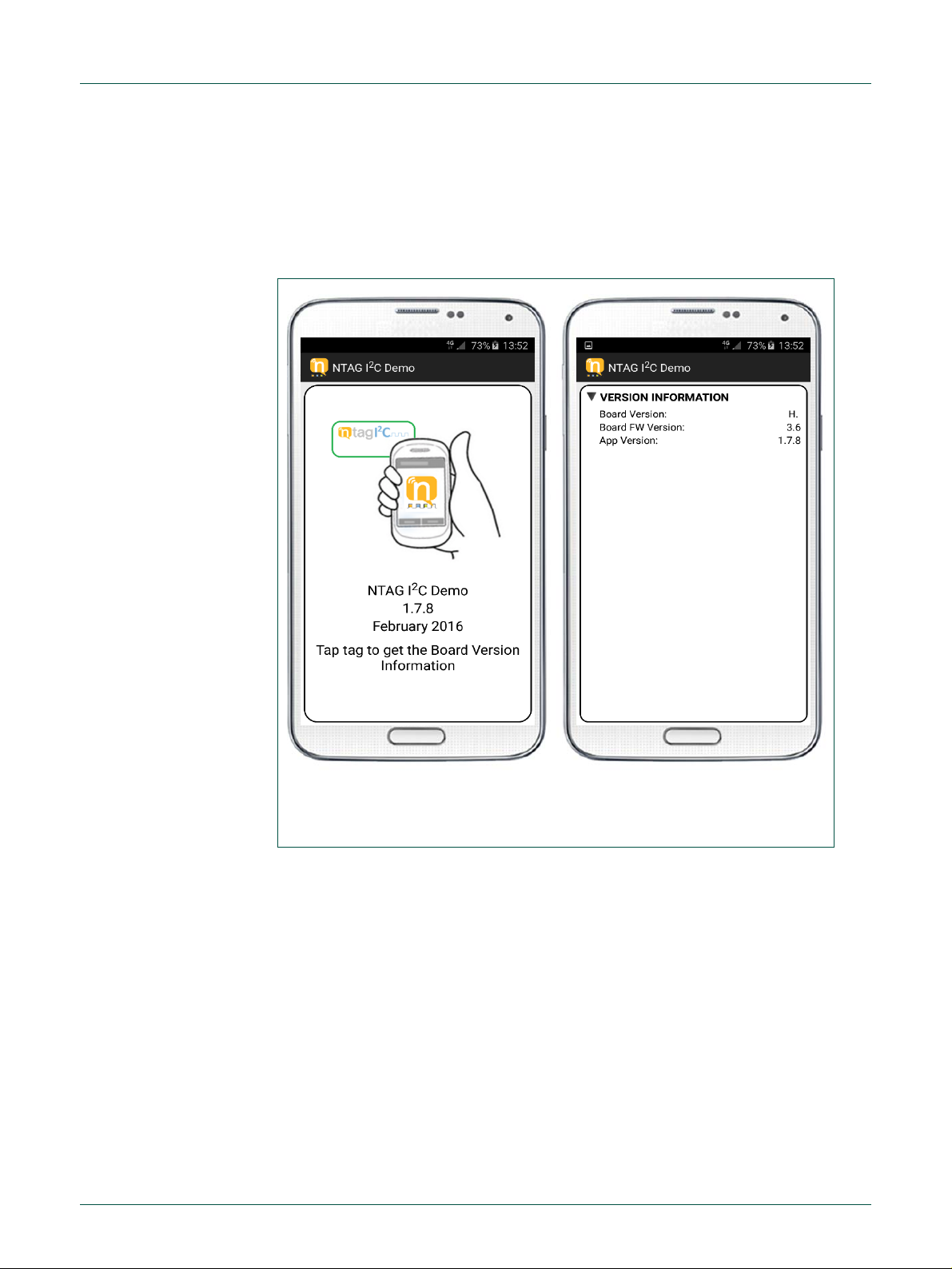
4.5.2 About
The about functiona lity can be used to get the vers ion being used for th e board design,
firmware of the boar d and the Android app by tapping the board wit h the NFC enabled
device.
4.5.3 Feedback
This option allows you to report feed back on the Android app direc tly to the NXP suppor t
team.
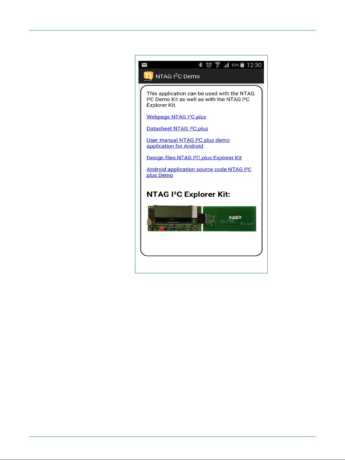
4.5.4 Learn more
This option will bring you to a set of links w ith further information ab out NXP NTAG I2C
plus tag, application notes, and design files and to the Android app source code.
All these functions can be found in the context menu
Page 45
SECURITY
STATUS
NXP Semiconductors
UM10966
NTAG I²C plus Explorer Kit - Android Demo
UM10966
All information provided in this docum ent is subject to legal disclaimers.
© NXP Semiconductors N.V. 2017. All rights reserved.
User manual
COMPANY PUBLIC
Rev. 2.1 — 09 March 2017
360121
45 of 55
Fig 39. Learn more snapshot
Page 46

SECURITY
STATUS
NXP Semiconductors
UM10966
NTAG I²C plus Explorer Kit - Android Demo
UM10966
All information provided in this docum ent is subject to legal disclaimers.
© NXP Semiconductors N.V. 2017. All rights reserved.
User manual
COMPANY PUBLIC
Rev. 2.1 — 09 March 2017
360121
46 of 55
4.6 Authentication
The NTAG I2C Plus offers authenticati on to protect memor y operations. The device can
be locked or not. If it is not lock ed, the user is able to perf orm any mem ory operation. If
the device is lock ed, the user must introduce t he correct password to authent icate and
access the memory.
The application provides the feature to lock and unloc k the device. In t he up per right side
of the screen there is a locker icon. In case the device is a NTAG I
authentication feature, the locker will be white and open. This means, the user can
interact will all m emor y. Nonetheless , if th e dev ice is a NT G I
are possible: the de vice can be loc ked or unl ocked, and th e device ca n be aut henticated
or not. In the case, the device is unlocked, there is no need of authentication. This is
shown with an open green loc ker. On the other side, if the device is locked, for a nonauthenticated stat e, the icon shown is a r e d cl os ed locker, while if it is auth enticated then
is a green closed locker. The different states are shown in Fig. 40.
2
C plus, the follo wing s tates
2
C, which has no
Page 47

SECURITY
STATUS
NXP Semiconductors
UM10966
NTAG I²C plus Explorer Kit - Android Demo
UM10966
All information provided in this docum ent is subject to legal disclaimers.
© NXP Semiconductors N.V. 2017. All rights reserved.
User manual
COMPANY PUBLIC
Rev. 2.1 — 09 March 2017
360121
47 of 55
Fig 40. Authentication States snapshot. (a) NTAG I2C Tag without authentication feature.
: (b) unlocked, (c) locked and authenticated, and (d)
locked and not authenticated.
(a) (b)
( c) (d)
The rest are NTAG I2C plus
Page 48

SECURITY
STATUS
NXP Semiconductors
UM10966
NTAG I²C plus Explorer Kit - Android Demo
UM10966
All information provided in this docum ent is subject to legal disclaimers.
© NXP Semiconductors N.V. 2017. All rights reserved.
User manual
COMPANY PUBLIC
Rev. 2.1 — 09 March 2017
360121
48 of 55
Fig 41. Password snapshot
Fig 42. Authentication state diagram
In order to lock or unlock the device, the user can press on the locker icon. A password
selection menu wi ll be shown, as shown in Fig. 41. If the device is unlock ed, then the
menu is to set a password. After setting it, the device is locked and authenticated. In
case the device is locked, the menu is to authentic ate the us er with the cor rec t pa s s word.
If the user introduces the correct password, the device is unlocked. Fig 42. depicts a
state diagram about the authentication procedure.
Page 49
SECURITY
STATUS
NXP Semiconductors
UM10966
NTAG I²C plus Explorer Kit - Android Demo
UM10966
All information provided in this docum ent is subject to legal disclaimers.
© NXP Semiconductors N.V. 2017. All rights reserved.
User manual
COMPANY PUBLIC
Rev. 2.1 — 09 March 2017
360121
49 of 55
Fig 43. Bluetooth pairing pop-up message
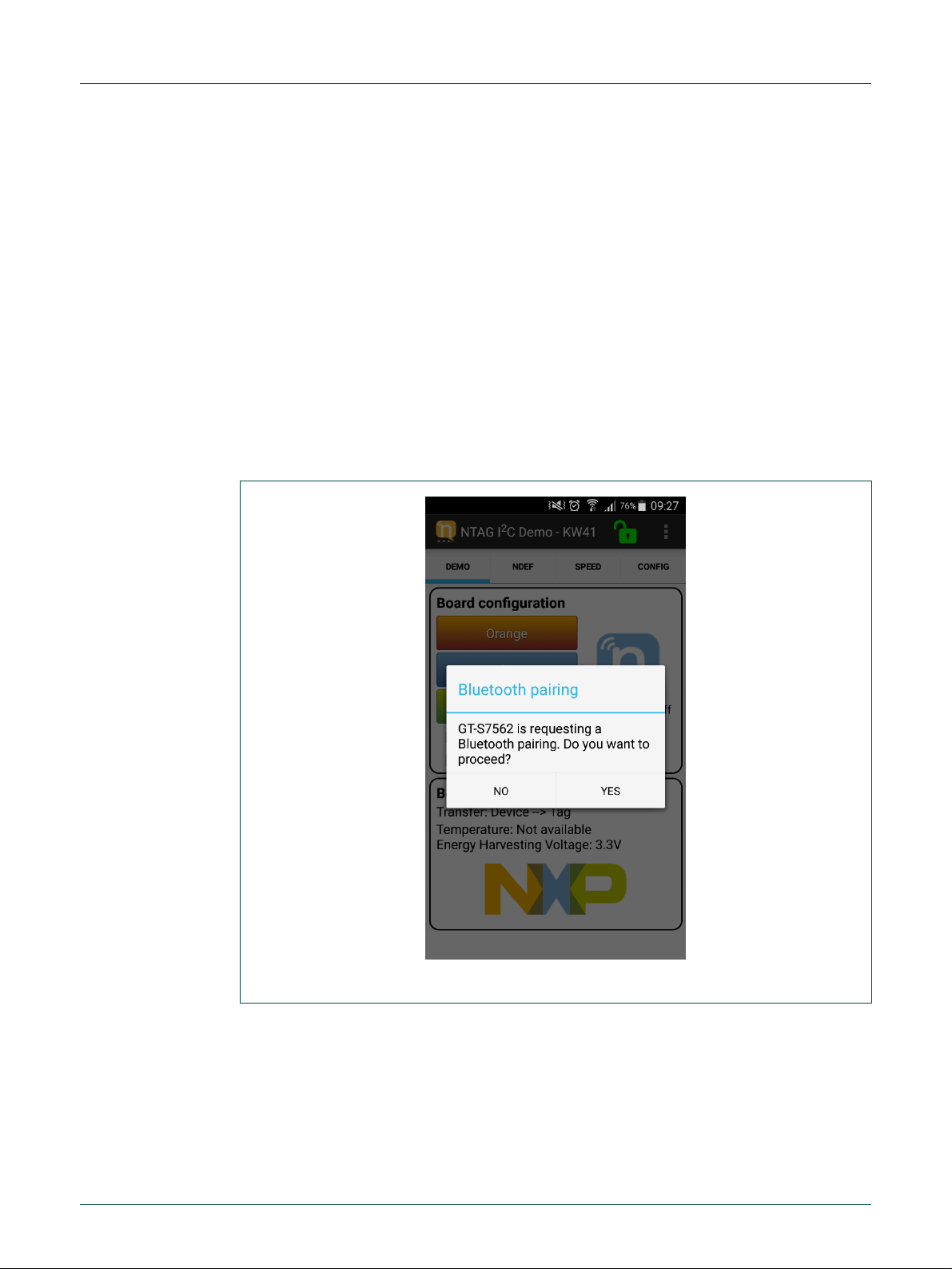
4.7 Bluetooth pairing functionality
This new feature is included in version 1.1 of the Android App. When working with a
Kinetis KW41Z board, a Bluetooth pairing NDEF message can be automatically written in
the NTAG I²C plus when pressing button ‘SW3’ on the board.
This Bluetooth pairing NDEF message is detected by the Android App when tapping the
NTAG I²C plus board to the phone. Once the NDEF message has been read by the
Android App, the NTAG I²C plus will delete it and write the default NDEF message.
A pop-up message is displayed on the phone to let the user decide, whether to proceed
to the Bluetooth pairing or ignore it. Fig 43 s ho ws the pop-up message displayed. If the
user decides to proceed with the Bluetooth pairing, the Andro id S ystem will pair both
devices and launch ‘Kinetis BLE Toolbox’ application from Play Store.
When using this functionality, this functionality is not restricted to NTAG I²C plus, it works
also with the previous NTAG I²C IC version.
Page 50
SECURITY
STATUS
NXP Semiconductors
UM10966
NTAG I²C plus Explorer Kit - Android Demo
UM10966
All information provided in this docum ent is subject to legal disclaimers.
© NXP Semiconductors N.V. 2017. All rights reserved.
User manual
COMPANY PUBLIC
Rev. 2.1 — 09 March 2017
360121
50 of 55
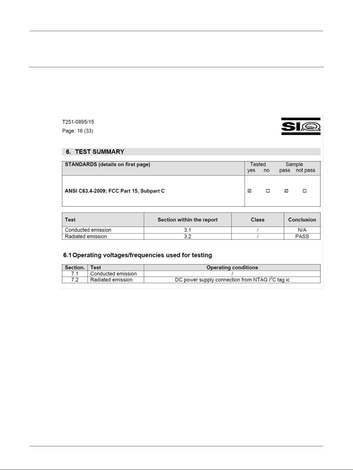
5. Federal Communication Com mi s s ion Interference Statement
5.1 FCC Grant
The NTAG I²C plus Explorer Kit with FCC ID OWROM5569-NT322E has been tested to
fulfil the approval requirements ANSI C63.4-2009; FCC Part 15, Subpart C and has
passed the tests.
5.2 Integration condition
NTAG I²C plus Explorer Kit is not intended to be reused as a module for integration into
end devices. If used, FCC certification needs to be repeated.
Page 51

SECURITY
STATUS
NXP Semiconductors
UM10966
NTAG I²C plus Explorer Kit - Android Demo
UM10966
All information provided in this docum ent is subject to legal disclaimers.
© NXP Semiconductors N.V. 2017. All rights reserved.
User manual
COMPANY PUBLIC
Rev. 2.1 — 09 March 2017
360121
51 of 55
6. References
[NTAGI2Cplus] NT3H2111/NT3H2211, NTAG I²C plus, NFC Forum Type 2 Tag
compliant IC with I²C interface
http://www.nxp.com/documents/data_sheet/NT3H2111_2211.pdf
[DEMOBOARD] Demo board home page with all resources
www.nxp.com/demoboard/OM5569
[EXPLORER] Schematics of the Explorer main board
http://www.nxp.com/documents/software/SW3638.zip
[Flex Antenna] Schematics of the Flex antenna
http://www.nxp.com/documents/software/SW3641.zip
[PCB Antenna] Schematics of the PCB antenna board
http://www.nxp.com/documents/software/SW3639.zip
[Field Detector] Schematics of the Field detector board
http://www.nxp.com/documents/software/SW3640.zip
[Identiv] Identiv Reader Driver
http://www.nxp.com/documents/software/SW3750.zip
[PC App] PC Applicatio n
http://www.nxp.com/documents/software/SW3651.zip
[Peek&Poke] Peek and Poke
http://www.nxp.com/documents/software/SW3652.zip
[LPC11U24] LPC11U24, 32-bit ARM Cortex-M0 microcontroller; up to 32 kB flash;
up to 10 kB SRAM and 4 kB EEPROM; USB device; USART
http://www.nxp.com/documents/data_sheet/LPC11U2X.pdf
[LM75B] LM75B, Digital temperature sensor and thermal watchdog
http://www.nxp.com/documents/data_sheet/LM75B.pdf
Page 52

SECURITY
STATUS
NXP Semiconductors
UM10966
NTAG I²C plus Explorer Kit - Android Demo
UM10966
All information provided in this docum ent is subject to legal disclaimers.
© NXP Semiconductors N.V. 2017. All rights reserved.
User manual
COMPANY PUBLIC
Rev. 2.1 — 09 March 2017
360121
52 of 55
[UM10989] NTAG I²C Demo Android app Developer start-up guide
www.nxp.com/documents/user_manual/UM10989.pdf
[UM10967] NTAG I²C plus Explorer Kit and Peek & Poke
www.nxp.com/documents/user_manual/UM10967.pdf
Page 53

SECURITY
STATUS
NXP Semiconductors
UM10966
NTAG I²C plus Explorer Kit - Android Demo
UM10966
All information provided in this docum ent is subject to legal disclaimers.
© NXP Semiconductors N.V. 2017. All rights reserved.
User manual
COMPANY PUBLIC
Rev. 2.1 — 09 March 2017
360121
53 of 55
Purchase of NXP ICs with NFC technology
Purchase of an NXP Semiconductors IC that complies with one of the Near
whether hardware or software.
7. Legal information
7.1 Definitions
Draft — The document is a draft version only. The content is still under
internal review and subject to formal approval, which may result in
modifications or additions. NXP Semiconductors does not give any
representations or war ra nti e s as to th e accu racy or completeness of
information included herein and shall have no liability for the consequences
of use of such information.
7.2 Disclaimers
Limited warranty and liability — Information in this document is believed to
be accurate and reliable. However, NXP Semiconductors does not give any
representations or warranties, expressed or implied, as to the accuracy or
completeness of such information and shall have no liability for the
consequences of use of such information. NXP Semiconductors takes no
responsibility for the content in this document if provided by an information
source outside of NXP Semiconductors.
In no event shall NXP Semiconductors be liable for any indirect, incidental,
punitive, special or consequential damages (including - without limitation lost profits, lost savings, business interruption, costs related to the removal or
replacement of any products or rework charges) whether or not such
damages are based on tort (including n egl ig ence), warranty, breach of
contract or any other legal theory.
Notwithstanding any damages that customer might incur for any reason
whatsoever, NXP Semiconductors’ aggregate and cumulative liability
towards customer for the products described herein shall be limited in
accordance with the Terms and conditions of commercial sale of NXP
Semiconductors.
Right to make changes — NXP Semiconductors reserves the right to make
changes to information published in this document, including without
limitation specifica ti on s and pr od uct de scri pti ons, at any time and without
notice. This document supersedes and replaces all information supplied prior
to the publication hereof .
Suitability fo r use — NXP Semiconductors products are not designed,
authorized or warranted to be suitable for use in life support, life-critical or
safety-critical systems or equipment, nor in applications where failure or
malfunction of an NXP Semiconductors product can reasonably be expected
to result in personal injury, death or severe property or environmental
damage. NXP Semiconductors and its suppliers accept no liability for
inclusion and/or use of NXP Semiconductors products in such equipment or
applications and therefore such inclusion and/or use is at the customer’s
own risk.
Applications — Applications that are described herein for any of these
products are for illustrative purposes only. NXP Semiconductors makes no
representation or warranty that such applications will be suitable for the
specified use without further testing or modification.
Customers are responsible for the design and operation of their applications
and products using NXP Semiconductors products, and NXP
Semiconductors acc ept s no liabi li t y for any assistance with applicati ons or
customer product design. It is customer’s sole responsibility to determine
whether the NXP Semiconductors product is suitable and fit for the
customer’s applications and products planned, as well as for the planned
application and use of customer’s third party customer(s). Customers should
provide appropriate design and operating safeguards to minimize the risks
associated with their applications and products.
NXP Semiconductors does not accept any liability related to any default,
damage, costs or problem whic h is bas ed on an y weak n ess or def ault in the
customer’s applications or products, or the application or use by customer’s
third party customer(s). Customer is responsible for doing all necessary
testing for the customer’s applications and products using NXP
Semiconductors products in order to avoid a default of the ap pli cations and
the products or of the application or use by customer’s third party
customer(s). NXP does not accept any liability in this respect.
Export control — This document as well as the item ( s) described herein
may be subject to export control regulations. Export might require a prior
authorization from competent authorities.
Translations — A non-English (translated) version of a document is for
reference only. The English version shall prevail in case of any discrepancy
between the translated and English versions.
Evaluation pro du ct s — This product is provided on an “as is” and “with all
faults” basis for evaluation purposes only. NXP Semiconductors, its affiliates
and their suppliers expressly disclaim all warranties, whether express,
implied or statutory, including but not limited to the implied warranties of noninfringement, merchantability and fitness for a particular purpose. The entire
risk as to the quality, or arising out of the use or performance, of this product
remains with customer.
In no event shall NXP Semiconductors, its affiliates or their suppliers be
liable to customer for any special, indirect, consequential, punitive or
incidental damages (including without limitation damages for loss of
business, business interruption, loss of use, loss of data or info rm ati o n, and
the like) arising out the use of or inability to use the product, whether or not
based on tort (including negligence), strict liability, breach of contract, breach
of warranty or any other theor y, even if advised of the possibilit y of suc h
damages.
Notwithstanding any damages that customer might incur for any reason
whatsoever (including without limitation, all damages referenced above and
all direct or general damages), the entire liability of NXP Semiconductors, its
affiliates and their suppliers and customer’s exclusive remedy for all of the
foregoing shall be limited to actual damages incurred by customer based on
reasonable reliance up to the greater of the amount actually paid by
customer for the product or five dollars (US$5.00). The foregoing limitations,
exclusions and disclaimers shall apply to the maximum extent permitted by
applicable law, even if any remedy fails of its essential purpose.
7.3 Licenses
Field Communicatio n (NFC ) st an da rds ISO / IEC 18092 and ISO/IEC 21481
does not convey an implied license under any patent right infringed by
implementation of any of those standards. Purchase of NXP
Semiconductors IC does not include a license to any NXP patent (or other
IP right) covering combinations of those products with other products,
7.4 Trademarks
Notice: All referenced brands, product names, service names and
trademarks are property of their respective owners.
MIFARE — is a trademark of NXP Semiconductors N.V.
I²C-bus — logo is a trademark of NXP Semiconductors N.V
Page 54

SECURITY
STATUS
NXP Semiconductors
UM10966
NTAG I²C plus Explorer Kit - Android Demo
UM10966
All information provided in this docum ent is subject to legal disclaimers.
© NXP Semiconductors N.V. 2017. All rights reserved.
User manual
COMPANY PUBLIC
Rev. 2.1 — 09 March 2017
360121
54 of 55
8. List of figures
Fig 1. NTAG I2C plus .................................................. 4
Fig 2. NTAG I2C plus Explorer Board (refer to
[EXPLORER]) ................................................... 5
Fig 3. PCB and Flex antenna boards with NTAG I²C
plus IC ............................................................... 6
Fig 4. Field detector board .......................................... 6
Fig 5. Identiv uTrust CLOUD 3700F reader ................ 7
Fig 6. Android app GUI ............................................... 9
Fig 7. Windows application GUI ................................ 10
Fig 8. Peek and Poke GUI ........................................ 11
Fig 9. Application overview ....................................... 12
Fig 10. Demo tab snapshot ......................................... 13
Fig 11. Green LED board configuration selection ....... 14
Fig 12. Reading board input ........................................ 15
Fig 13. Temperature sensor demonstrates SRAM pass
through mode .................................................. 16
Fig 14. Enabling NEK board LCD ............................... 17
Fig 15. Displaying NDEF text message on NEK board
LCD ................................................................. 18
Fig 16. NDEF tab snapshot ......................................... 20
Fig 17. Reading NDEF message stored in EEPROM of
Fig 18. Writing NDEF message to NTAG I2C plus
Fig 19. Data transfer speed mea sur ement concept
Fig 20. SRAM Speed test snapshot ............................ 24
Fig 21. EEPROM Speed test snapshot ....................... 25
Fig 22. CONFIG tab menu .......................................... 26
Fig 23. Read tag memory snapshot ............................ 27
Fig 24. Reset tag snapsh ot ......................................... 28
Fig 25. Alternative way to reset tag ............................. 29
Fig 26. Read Session registers snapshot ................... 30
Fig 27. Read / Write configuration registers snapshot 32
Fig 28. Figure title here ............................................... 35
Fig 29. LPC11U1x/2x flash sectors ............................. 35
Fig 30. On-chip flash memory organization for NFC
Fig 31. NFC Flashing option selection within the
Fig 32. Selection of binary file to be flashed into MCU
Fig 33. Selection of binary file to be flashed into MCU
Fig 34. Entering NFC Flashing mode .......................... 40
Fig 35. NFC Flashing progress bar ............................. 41
Fig 36. NFC Flashing successful execution ................ 42
2
NTAG I
EEPROM ........................................................ 22
behind the SRAM selection ............................. 23
flashing functionality ........................................ 37
Android app..................................................... 38
memory ........................................................... 39
memory (II) ...................................................... 40
C plus ................................................ 21
Fig 37. LED Blinker NFC Flashing upgrade verification
........................................................................ 43
Fig 38. About tab snapsho t ......................................... 44
Fig 39. Learn more snapshot ...................................... 45
Fig 40. Authentication States snapshot. (a) NTAG I2C
Tag without authentication feature. The rest are
NTAG I2C plus: (b) unlocked, (c) locked and
authenticated, and (d) locked and not
authenticated. .................................................. 47
Fig 41. Password snapshot ......................................... 48
Fig 42. Authentic at io n state dia gram ........................... 48
Fig 43. Bluetooth pair i ng pop-up message .................. 49
Page 55

SECURITY
STATUS
NXP Semiconductors
UM10966
NTAG I²C plus Explorer Kit - Android Demo
Please be aware that important notices concerning this document and the product(s)
described herein, have been included in the section 'Legal information'.
©
For more information, please visit: http://www.nxp.com
09 March 2017 360121
UM10966
9. Contents
1. Object ................................................................... 3
2. NTAG I2C plus introduction ................................ 4
3. NTAG I2C plus Explorer kit contents ................. 5
3.1 Hardware components ....................................... 5
3.1.1 NTAG I2C plus Explorer Board ........................... 5
3.1.2 Antenna board .................................................... 6
3.1.3 Field detector board ........................................... 6
3.1.4 USB reader ........................................................ 7
3.1.4.1 USB Reader firmware update ............................ 8
3.2 Software components ........................................ 8
3.2.1 NTAG I2C plus Explorer board firmware ............. 8
3.2.2 Android app ........................................................ 8
3.2.3 Windows app ...................................................... 9
3.2.4 Peek and Poke GUI ......................................... 10
4. NTAG I2C plus Explorer Demo app .................. 12
4.1 Demo tab.......................................................... 12
4.1.1 Configuring NEK board to demonstrate RF to I2C
communication ................................................. 14
4.1.2 Reading board input to demonstrate I2C to RF
communication ................................................. 15
4.1.3 Temperature sensor ......................................... 16
4.1.4 Enabling LCD display ....................................... 17
4.1.5 Displaying NDEF text message on the NEK
board LCD ........................................................ 18
4.2 NDEF ta b ......................................................... 19
4.2.1 Reading NDEF data ......................................... 21
4.2.2 Writing NDEF d ata ........................................... 22
4.3 Speed tab ......................................................... 23
4.3.1 SRAM speed test ............................................. 23
4.3.2 EEPROM speed test ........................................ 25
4.4 Configuration tab .............................................. 26
4.4.1 Reading tag memory ........................................ 27
4.4.2 Resetting tag me mory ...................................... 28
4.4.3 Reading session registers ................................ 30
4.4.4 Reading / Writing configuration registers ......... 32
4.5 Action bar ......................................................... 35
4.5.1 NFC Flashing via NTAG I2C plus Explorer demo
......................................................................... 35
4.5.1.1 Design implementation choice ......................... 35
4.5.1.2 How to flash new firmware through NFC .......... 38
4.5.2 About ................................................................ 44
4.5.3 Feedback ......................................................... 44
4.5.4 Learn more ....................................................... 44
4.6 Authentication .................................................. 46
4.7 Bluetooth pairing functionality .......................... 49
5. Federal Communication Commission
Interference Statement ...................................... 50
5.1 FCC Gran t ........................................................ 50
5.2 Integration condition ......................................... 50
6. References ......................................................... 51
7. Legal information .............................................. 53
7.1 Definitions ......................................................... 53
7.2 Disclaimers ....................................................... 53
7.3 Licenses ........................................................... 53
7.4 Trademarks ...................................................... 53
8. List of figures ..................................................... 54
9. Contents ............................................................. 55
Date of release:
NXP Semiconductors N.V. 2017. All rights reserved.
Document identifier:
Page 56

Mouser Electronics
Authorized Distributor
Click to View Pricing, Inventory, Delivery & Lifecycle Information:
NXP:
OM23221ARD
 Loading...