

Page 1

Freescale Semiconductor
Reference Manual
MSC711xADSRM
Rev. 1, 6/2007
MSC711x Application Development
System (MSC711xADS) Reference
Manual
MSC7110, MSC7112, MSC7113, MSC7115, MSC 7116, MSC7118,
MSC7119
The MSC711xADS board uses one StarCore™-based 16-bit
MSC711x proce ssor, the MSC7116, along with the
PowerQUICC II ™ MPC8272 as the host processor. The
MSC711xADS board serves as a platform for software and
hardware development in the MSC711x environment.
Developers can use on-board resources and the associated
debugger to perform a variety of tasks, such as downloading
and running code, setting breakpoints, displaying memory and
registers, and connecting proprietary hardware via the
expansion connectors. The MSC711xADS board can also
function as a demonstrati on system, with application software
programmed into its Flash memory.
The board works seamlessly with an evalua tion copy of
CodeWarrior® Development S tudio. The MSC711x family is a
high-performanc e, cost-effective family of DSPs based on the
StarCore
flexibilit y with pe riphe rals a nd performanc e, and over all system
cost savings. Devices in the MSC711x family target highbandwidth highly computat ional DSP applications and are
optimized for packet tele phony a pplications, providing a
competitive price per ch annel for voice over packet systems.
Designed with attenti on to system requirements from the start,
the MSC711x family de livers one core architecture for digita l
signal processing that spans the low to high end.
This manual is an operation gui de for the MSC71 1 xADS board.
It describes the board architecture and functionali ty and
provides instruc tions on how to use the board.
SC1400 core, which offers system solutions,
CONTENTS
1 Overvi ew ........... .............. .............. ........... ............. ..3
1.1 How the MSC711xADS Works ..............................6
1.2 Produc t Do cu m e nt at io n ........ ... ... ................ ... ... .......6
1.3 Third-Party Documentation .................................... 7
2 Hardwar e C onfigura tio n an d Boo t ...... ... ................. 9
2.1 Board Un pa c ki ng ...... ... ... ........ ... ... ................ ... ... ....9
2.2 Board In s ta lla ti o n ......... ... ........ ... ... ................ ... ... ....9
2.3 Board Co nf ig u ra tio n ....... ........ ... ... ................ ... ... ..1 0
2.4 DIP-Switch and Jumper Settings ..........................10
2.5 MSC711xADS Boot .............................................18
2.6 Board Co nt ro ls and Indic at or s ........ ................. ... ..2 0
3 Board-Level Functions ..........................................23
3.1 Reset . ......... ........ ...... ........ ........ ...... ........ ........ ........2 3
3.2 Clocking................................................................ 24
3.3 Power Supply ........................................................ 27
4 Memory Map/Programming Model ......................29
4.1 Memory Map .........................................................29
4.2 Board Control and Status Registers (BCSRx) ......30
5 MSC711xADS Interfaces .....................................37
5.1 HDI16 Host Processor Interface ...........................37
5.2 60x Bus Buffering .................................................40
5.3 MSC711x Connection to the MPC8272 ...............40
5.4 RS-232 P or ts ..... ... ........ ... ... ................ ... ... .............41
5.5 JTAG/ OC E 10 Test Access P or t (T A P ) .... ............. 4 2
5.6 DDR SDRAM Interface ........................................44
5.7 Ethern et ............. ................. ...................... ............. 45
5.8 Synch rono u s D RA M (6 0x B us ) ......... ... ................46
5.9 Flash Memory .......................................................48
5.10 Time-Slot Interchanger (TSI).................................49
5.11 SLIC SLA C In te rface ... ........ ... ... ................ ... ... .....49
5.12 E1/T1 Framer ........................................................50
© Freescale Semiconductor, Inc., 2005, 2007. All rights reserved.
Page 2

MSC711x Application Development System (MSC711xADS) Reference Manual, Rev. 1
Page 3

Overvi ew 1
Table 1-1 lists the feat ures , components, an d specificatio ns of the MSC711xADS board.
Table 1-1. Features of the MSC711xADS Boar d
Feature Description
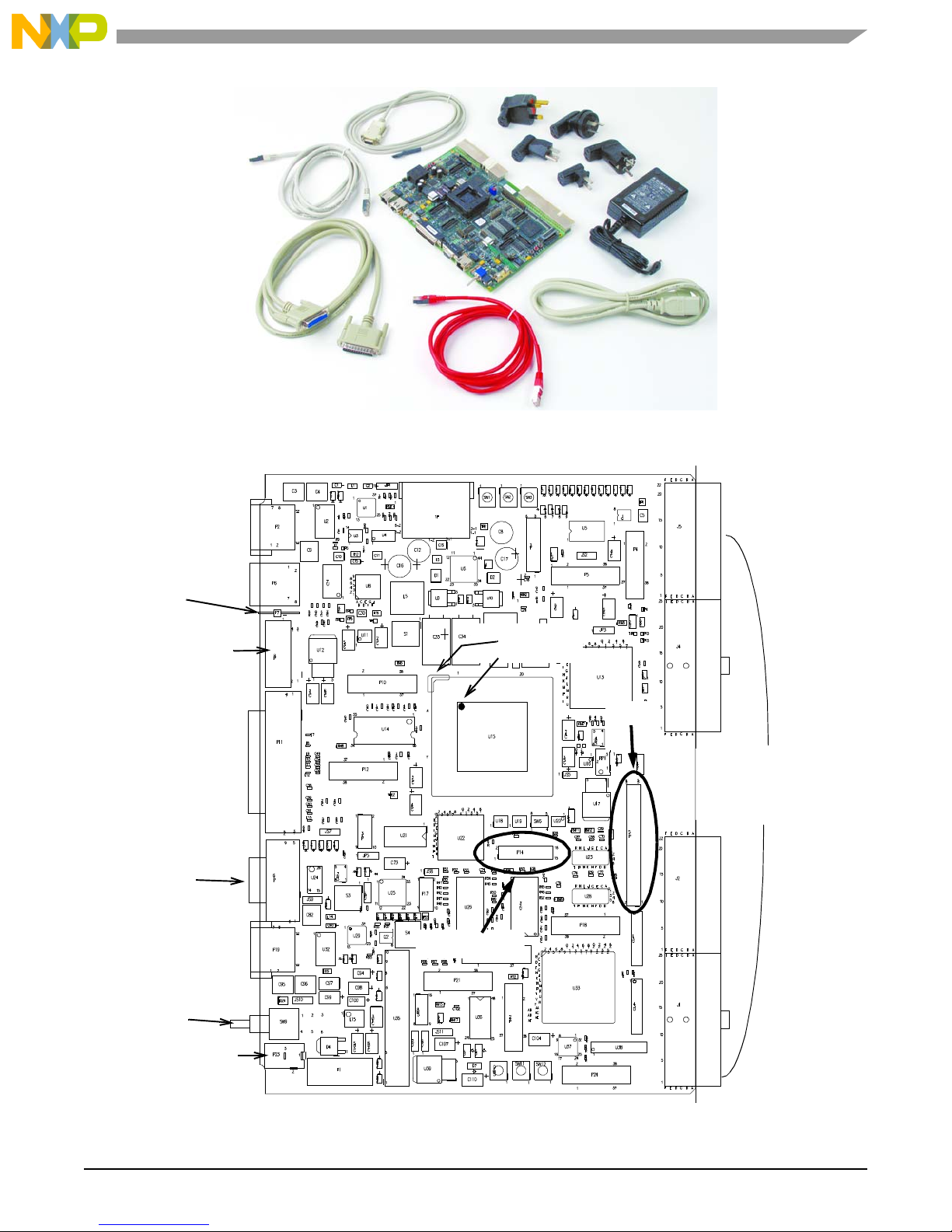
Kit contents (see Figure 1-1):
Full-Featured
Development Kit
Board
Specifications
MSC7116 Device
• MSC711xADS board.
• Evaluati on copy of CodeWarrior Developm ent St udio
• User documen tation.
• Power supply and cables.
• Operating temperature: 0° C to 70° C (room temperature).
• Storage temperature: –25° C to 85° C.
• Dimensions: One single-slot 6U PCI form factor.
• Relativ e hum idi ty: 5% to 90% (non-condensin g)
• +12 V external DC power supply rate for a maximum current of 1.8 A.
•Functionality:
—SC1400 DSP core.
—800 MMACS at 200 MHz.
—408 KB total memory.
—Two time-division multiplex (TDM) interfaces, 128-channels each.
—10/100 Ethernet MAC.
—32-channel DMA controller.
—AHB-Lite internal bus.
—DDR external memory controller interface.
—16-bit enhanced host port.
—JTAG/OCE10 emulator test.
• Process/Voltage:
—0.13 μ, 1.2 V core; 2.5 V–3.3 V I/O
• Power Consumption:
—300 to 400 mW target (200 MHz).
• Packaging
—Pb-free 400 MAPBGA (17 × 17 mm, 0.8 mm pitch).
—Footprint-compatibl e with MSC7110, MSC7112, MSC7113, and MSC7115
• 100 MHz bus frequency, 200 MHz CPM frequency, and 400 MHz over all frequency.
• Efficient , dual-core architec ture that combines the PowerPC 603e ecore® with a separate RISCbased communicat ions processor module.
• Superior integration with featu res optimized for cost-s ensitive designs and sec uri ty-oriented
MPC8272
MSC711x Application Development System (MSC711xADS) Reference Manual, Rev. 1
networking applications.
• Economical, powerful integrat ed security engine that supports industry-standard encryption
algorithms.
• Smooth migration path for PowerQUICC™ and PowerQUICC II™ processor-based designs.
• Strong third-party tools support through the Freescale Smart Networks Alliance Program me mb ers.
Page 4

Overview
Table 1-1. Features of the MSC711xADS Board (Continued)
Feature Description
• MPC8272 is the MSC711x host. The MPC8272 system bus connects t o the MSC711x HDI.
• Host/Slave connection through the 16-bit HDI16 port; the HDI16 interface is accessible via a PCI
backplane multiplexed with PCI signals.
• 32-bit PCI host compatible.
• Host debug thr ough a single JTAG connector suppor ts both the MPC8272 and MSC711x
processors.
• Debugging via either one JTAG chain (MPC8272 and MSC711x device together) or two
independent JTAG connections (MPC8272 separat e fr om the MSC711x device) through the
COP/JTAG connection or the parallel port command converter.
• Flash memory for stand-alone applications.
• Memory:
—8 MB Flash memory for the MPC8272 (16 bits wide).
—64 MB SDR SDRAM for the MPC8272 (64 bits wide).
—32 MB DDR SDRAM for the MSC711x device (32 bits wide).
• Communicati ons ports/external connections (see Figure 1-2):
—10/100Base-T Ethernet port (MII/RMII) using Davicom DM9161 connected to the MSC711x
device.
—10/100Base-T Ethernet port using Davicom DM9161 connected to the MPC8272 device.
—T1/E1 TDM interface using PMC-Sier ra PM4351 connected to the TSI.
—Two PSTN connections using Legerity Le78D110VC/Le77D11xVC (SLI C/SLAC) connect ed to the
TSI.
MSC711xADS
—H.110.
—RS-232 universal asynchronous receiver/transmitter (UART) port (9-pin D-connector attached to
the MPC8272).
—RS-232 port (pins) connected to a UART that is connected to the MSC711x device.
—OCE10/JTAG connector for the MSC711x device.
—Parallel port that includes a JTAG command converter connected to the MP8272 device.
—COP/JTAG connector for the MPC8272.
—High-density (MICTOR) l ogic analyzer connectors to monitor MSC711x signals
—6U P C I fo rm fa c to r.
• MSC711x devices boot through the HDI16 host port or the I2C port.
• After reset, selectable Debug Enable/Disable and Debug Request opti ons.
• Board identification and board status read via the Board Control and Status Registers (BCSRx).
• Variant board configurations available via the dual-in-line package (DIP) switch setting.
• Push buttons for both the host and slave:
— Power-on reset.
—Soft reset.
—Hard reset.
— Abort.
• Time-slo t interchanger (TSI) devi ce connected to the TDM channels on the MSC711x processor;
used as the H110 framer and TDM master .
• SLIC-SLAC interf ace enables use of 6-line commun ication board with Voice-over-Broadband
SLIC/SLAC chip set.
• LEDs indicate power supply, peripheral enables, and software signals.
MSC711x Application Development System (MSC711xADS) Reference Manual, Rev. 1
Page 5
cPCI
(Backplane)
Connections
PSTN
Ports
Fast Ethernet
to MSC711x
E1/T1
RS-232
JTAG/OCE10
Parallel
Port
RS-232
Fast Ethernet
to MPC8272
(MPC8272)
(MSC711x)
MSC711x
Device
MPC8272
device
Power
Voltage Input
On/Off
Fuse
JTAG/COP
alignment
indicators
HDI
Figure 1-1. Full-Featured MSC711x Development Kit
Figure 1-2. MSC711xADS External Connections
MSC711x Application Development System (MSC711xADS) Reference Manual, Rev. 1
Page 6
Overview
Expansion Header
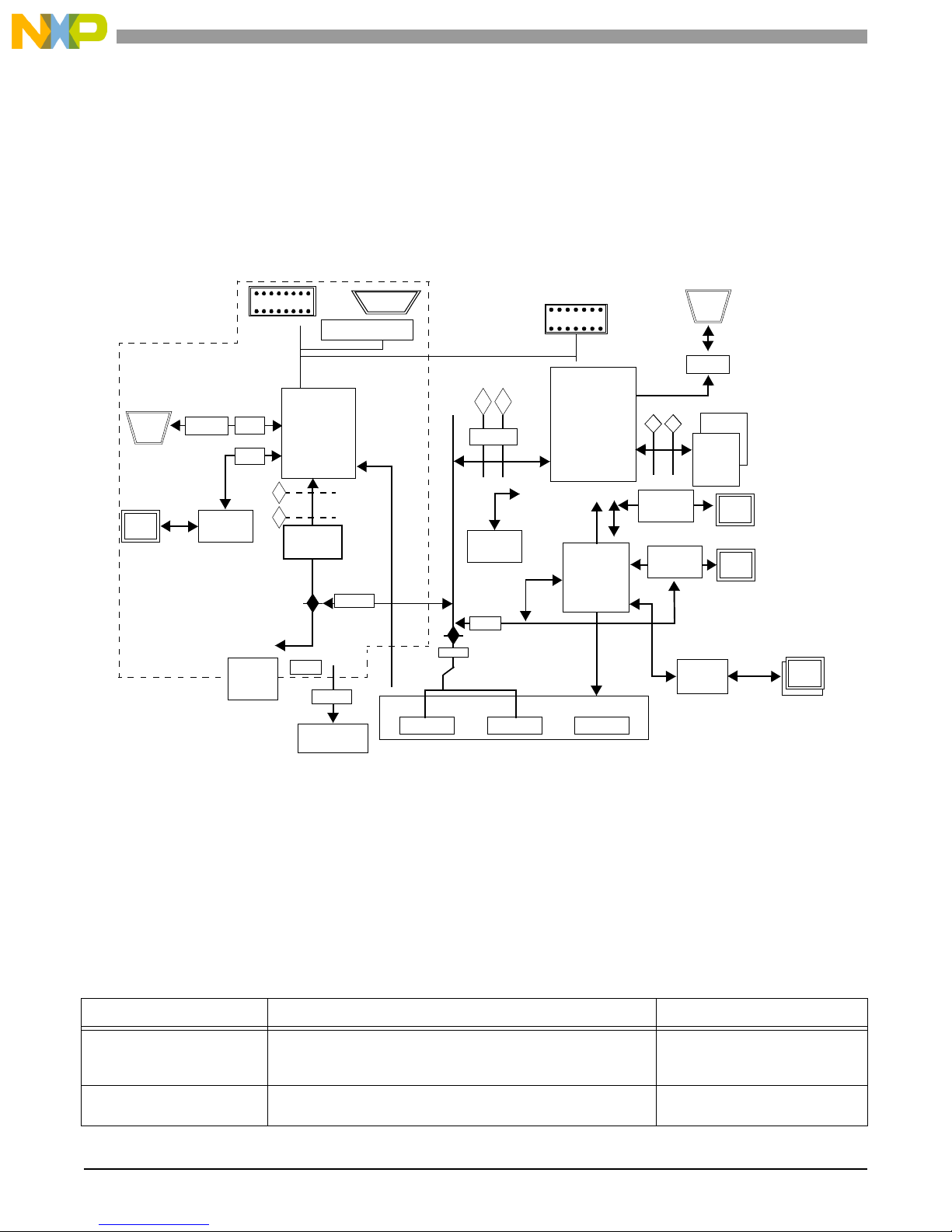
J1 J2 J4
H.110
MSC7116
OCE10
UART
DDR
HDI16
DDR
DDR
16 MB
16 Bits
MPC8272
PCI
COP
60x Bus
SDRAM
(64 MB)
512
TS Switch
RJ45
RJ45
10/100
PHY
RJ45
16/8 Bit
A D
16 Bit
SCC
FCC
RS-232
10/100
PHY
8 Bit
Flash
Memory
16 Bit
BCSR
T1/E1
Framer
8 Bit
SLICK
SLACK
RJ11
RS-232
9-Pin
9-Pin
16 Bit
I2C
EEPROM
D
A
B
A D
32
XB
60x Bus
Mictor
Mictor
TDM
MAC
2 TDM
Parallel
EPP-to-JTAG
OCE10
COP
1.1 How the MSC 711xAD S Works
The MSC711xADS allows the application engineer to upload software to both the MSC7116 and MPC8272
devices and run that software with emulated debugging devices (JTAG or a PC). The software applic ation can run
in a “bare bones” opera tion with only the MSC7116 and MP C8272 processors or with various input or output data
streams, such as from the E1/T1 connection, the Ethernet connections, or the PSTN connections. You can analyze
the results with the CodeWarr ior debugger or directly analyze the input or output data stream via other methods.
1.2 Product Docu ment ati on
Table 1-2 lists the documentation that supports the MSC711xADS. Documentation is available from a local
Freescale distributor, a Freescale semiconductor sales office, or a Freescale Literature Distribution Center. For
documentation update s, visit the Freescale DSP web site.
MSC711xADS Reference
Manual
MSC711x
Technical Data
Name Description Order Number
Detailed functio nal description of the MSC711xADS board,
including memory and per ipheral configuration, switch
settings, operation, connection s, and programming.
MSC711x features li st and physical, electrical, timing, and
package specifi cations
MSC711x Application Development System (MSC711xADS) Reference Manual, Rev. 1
Figure 1-3. MSC711xADS Block Diagram
Table 1-2. MSC711xADS Documentation
MSC711xADSRM
MSC711x
Page 7

Table 1-2. MSC711xADS Documentation (Continued)
Name Description Order Number
MSC711x
Reference Manual
MPC8272 PowerQUICC II™
Family Reference Manual
MPC8272 PowerQUICC II™
Family Hardware
Specifications
SC1000 Family Processor
Core Reference Manual
OCE10 On-Chip Emulator
Reference Manual
Application Notes Documents describi ng specific applications or optimized
Detailed functional description of the MS C711x m em ory and
peripheral configuration, operation, and register programming
Describes the functi onal operation of the MPC8227 2 wit h an
emphasis on peripheral functions.
Details on power considerations, DC/AC elect rical
characteris ti cs, and AC timing specificat ions for the
MPC8272 family of devices
Detailed description of the SC1000 family proc essor cores,
including the SC1400, and instruction set
Information on the architecture and programm ing model of
the OCE10 on-chip emulator, which is the StarCore
implementation of the EOnCE. The OCE10 on- chip emulator
is a peripheral that facilitates debugging the StarCore
SC1000-family processor core and peripherals.
device operation including code examples . Application notes
of particular inter est to d eveloper s worki ng with the MSC71 1x
board are as follows:
• AN2780, Getting Start ed With the MSC711x Application
Development System (MSC711xADS).
• AN2786, MSC711x Desi gn Checklist.
• AN2946, MSC711x Time-Division Multiplexing (TDM)
Usage Examples (with accompanying softwar e).
• AN2945, Booting an MSC711x Device from an MPC8272
Host Using the HDI16 Interfa ce.
• AN2893, MSC711x Memory Controller Usage Guidelines:
Supporting Double Data Rate (DDR) SDRAM Devices.
• AN2888, Glueless Packet Transpor t from PowerQUICC
Network Processor s to MSC711x DSP Devices.
• AN2715, Porting Code from the DSP56300 Family of
Products to the SC140/SC1400 Core.
.
Third-Party Documentation
MSC711xRM
MPC8272RM
MPC8272EC
10180-01
10055-03
Refer to the MSC711x product
pages on the Freescale
Semiconductor web si te.
1.3 Third-Party Docume ntatio n
• PMC-SIERRA PM4351 data sheet
• Infineon PEF20451 data sheet
• Davicom DM9161 data sheet
• Legerity SLIC/SLAC (Le78D110VC and Le77D11xVC) data sheet
MSC711x Application Development System (MSC711xADS) Reference Manual, Rev. 1
Page 8

Overview
MSC711x Application Development System (MSC711xADS) Reference Manual, Rev. 1
Page 9

Board Unpacking
Hardware Configuration and Boot 2
This chapter provides unpacking, installation, an d hardware preparation instructions for the MSC711xADS. It also
describes the boot procedure and familiarizes you with the board controls and indicators for use during board
operation.
2.1 Board Unpacking
The procedure for unpackin g the MSC711xADS board is as follows:
1. Unpack the equipment from the shipping carton. If the shipping carton is damaged upon receipt,
request that the carrier agent be present during unpacking and inspection of equipment.
2. Refer to the packing list and verify that all items are present.
3. Save the packing material for storing and reshipping equipment.
CAUTION: Avoid touching areas of the integrated circuitry; static discharge can damage
circuits.
2.2 Board Installati on
To install the MSC711xADS, perform the following steps:
1. Determ ine whet her t h e MSC 711xAD S i s to be acc es sed via a JTAG interface or a PC.
a. For JTAG, connect the JTAG device to the JTAG/COP header connect or (P14).
b. For a PC, install the CodeWarrior test software or any other compat ible debugging so ft ware on the
PC. The MSC711xADS is optimized for CodeWarrior test software.
2. Determine whether board operation is to be host- controlled or stand-alone. Make the connections and
configurations accor dingly, as described in
3. If the board is to be inserted into a cPCI rack, configure the JP7 jumper accordingly ( see Section 2.4.14
on page 17).
4. Prepare the equipment for testing. For example, if checking telecom, prepare the phone lines for the
lab, and so on.
5. Configure the MSC711xADS switches and jumpers as described in Section 2 . 4 on page 10 . The
switches and jumpers that must be configur ed before you can proceed to step 6 are as follows:
• RP1 (Core voltage, see Section 2.4.1 on page 12).
• SW6 (JTAG chain options, see Section 2.4.4 on page 13).
• SW7 (I2C EEPROM configuration options, see Section 2.4.5 on page 14).
• JP1 (Ethernet PHY MII/RMII mode, see Section 2.4.8 on page 15).
• Initialize the SDRAM (see Sectio n 5.8 .1 on page 47).
Section 2.3 on page 10.
6. Insert the MSC7116 DSP device into the indicated socket (see Figure 1-2 on page 5). Ensure that the
alignment indicator (a dot) on the device is next to the alignment indicator (a section of metal) on the
chip socket.
MSC711x Application Development System (MSC711xADS) Reference Manual, Rev. 1
Page 10

Hardware Configuration and Boot
7. Establish the appropriate external connections (for a list of external connections and their locations,
see
Figure 1-2 on page 5).
8. Turn on the MSC711xADS voltage (SW9, as sho wn in Figure 1-2 on page 5). Note that ON is up and
OFF is down. We recommend that you turn off the voltage if the MSC711xADS is unused for more
than 48 hours.
2.3 Board Configurati on
The MSC711xADS can be installe d for either host-controlled or stand-alone operation. In host- controlled
operation, the MPC8272 and the MSC711x processors are both controlled by a host computer and are connected
via a separate JTAG chain or a shared JTAG chain. Use the SW6 swit ch to con fig ur e the M SC 711xAD S JTAG
options (see
• Separate chain. The MPC8272 and the MSC711x processors each independe ntly connects to a JTAG command
converter. The MPC8272 connects via the JTAG/COP connec t or (P14) to a JTAG command converter or
through the parallel port conn ector (P11) to a PC and does not use an external JTAG command converter. The
MSC711x can directly connect through the JTAG/OCE10 connector (P8) via a JTAG command converter.
• Shared chain. Both the MPC8272 and MSC7116 processors share the same JTAG chain. The MPC8272 is the
first device in the chain, so either the JTAG command converter connects to it via the JTAG/COP connector
(P14) or it conne cts to a PC thr ough the parallel port connector (P11) with no use of an external JTAG command
converter. The debugging tool must support the shared JTAG chain option, as CodeWarrior does.
Section 2.4.4):
In stand-alone operation, the host computer controls the M S C711xADS board not through the JTAG port but
through one of its other ports, such as the RS-232 port or the fast Ethernet port. The applic ation program must be
programmed into the board Flash memory for the MPC8272 and into the board I2C EEPROM for the MSC7116.
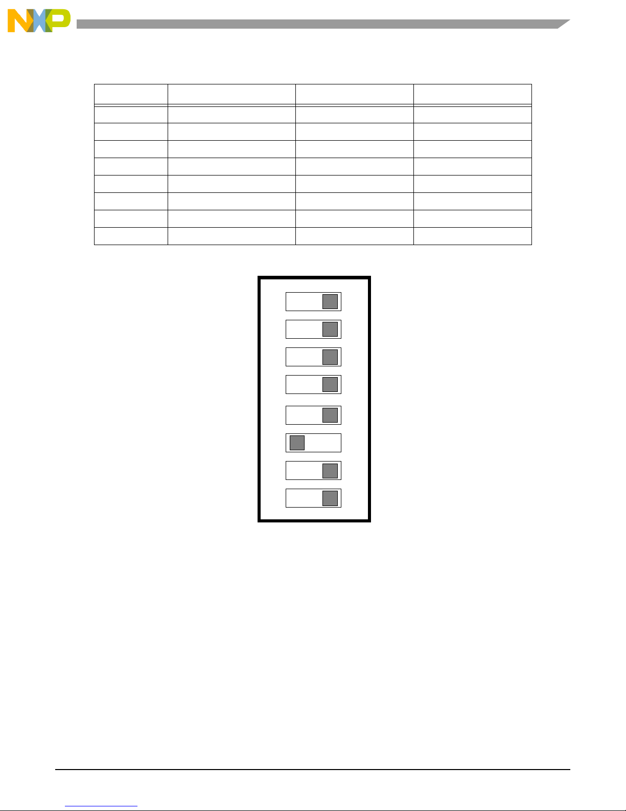
2.4 DIP-S witch and Ju mper Sett ing s
T o select the desired configuration and ensure proper operation of the MSC711xADS board, you may have to
change the DIP-Switch sett ings before installation. The location of the switches, indicators, DIP-Switches, and
connectors is illus trated in Figure 2-1. The board has been factory tested and is shipped with DIP-Switch settings
as described in the following pa ragraphs. Values can be changed for the following parameters :
• MSC711x internal voltage supply leve l via potentiometer (RP1). See Section 2.4.1 on page 12.
• MSC711x power-up configuration (SW4). See Section 2.4.2 on page 12.
• MSC711x event pin c onfiguration (SW5). See Section 2.4.3 on page 12.
• JTAG opt io n s (SW 6 ). Se e Section 2.4.4 on page 13.
• Select I2C EEPROM address and protection mode (SW7). See Section 2.4.5 on page 14.
• MPC8272 clock mode settings (SW8). See Section 2.4.6 on page 15.
• Main power switch (SW9). See Section 2.4 .7 on page 15.
• MSC711x Ethernet PHY MII/RMII mode (JP1). See Section 2.4.8 on page 15.
• H110 back plane reset (JP2). See Section 2.4.9 on page 16.
• TDM master selection (JP3). See Section 2.4.10 on page 16.
• MSC711x clock-in source (JP4). Section 2.4.11 on page 16.
• MPC8272 Hard Reset Configuration Word source (JP 5). Section 2.4.12 on page 17.
MSC711x Application Development System (MSC711xADS) Reference Manual, Rev. 1
Page 11
DIP-Switch and Jumper Settings
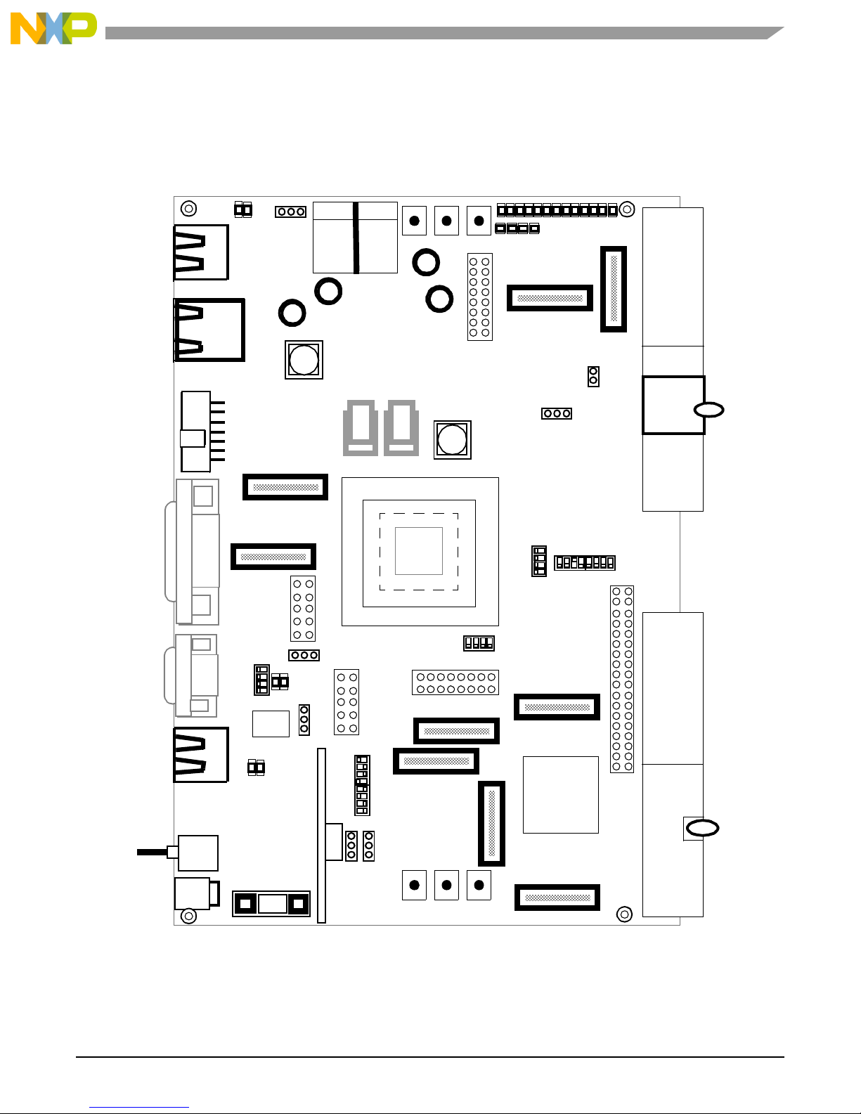
J1
J2
J4
J5
P2
P6
P8
P11
P16
P19
SW9
P23
SW10 SW11 SW12
P22
P24
P20
P21
P18
JP7 JP8
SW8
P17
P13
JP5
JP6
SW7
P14
SW6
P15
SW4
SW5
JP2
JP3
P12
P10
P4
P5
P3
SW1 SW2 SW3
JP1
P1
LD1 - LD13
LD16 - LD19
LD14 - LD15
LD27-28
LD25-26
• MPC8272 Hard Reset to MSC711x Hard Reset (JP6). See Section 2.4 . 13 on page 17.
• PCI expansion enable/disable (JP7). See Section 2.4.14 on page 17.
• Host (MPC8272) enable/disable (JP8). See Section 2.4.15 on page 18.
Figure 2-1. MSC711xADS Switch and Jumper Locations
MSC711x Application Development System (MSC711xADS) Reference Manual, Rev. 1
Page 12
Hardware Configuration and Boot
ON
4
3
2
1
10
2.4.1 Internal Voltage Supply Level (RP1)
The level of internal (cor e) volta ge is tuned via RP1 and is in the range of 0.8–1.5 V. You can measure voltage
across JS5 with a digital volt meter (DVM) or any other high input impedance voltage measurement devi ce. Core
voltage should be measured and tuned before the MSC711x processor is inserted into its socket.
2.4.2 MSC711x Power-Up Settings (SW4)
The SW4 switches contr ol the conf iguration f or th e MSC71 1x de vice. The se swit ches ar e contr olled th rough Boar d
Control Status Re gis t er 2 (BCSR2) (see
switch is in the ON position, its related signal is deasserted to 0. When the switch is in the OFF position, its relate d
signal is asserted to 1.
Switch BSCR2 Bit OFF ON
1 DBREQ 1 0
2 SWTE 1 0
3 BM1 1 0
Chapter 4, Memory Map/Programming Model, on page 29). When a
Table 2-1. SW4 Switch Settings
4 BM0 1 0
Figure 2-2. SW4 Factory Default Setting
2.4.3 MSC711x Event Pin Configurat ion (SW 5)
The SW5 switches control the configur ation of the MSC711x device and the EVNT[0–4] pins. When a switch is in
the ON position, its related signal is deasserted to 0. When the switch is in the OFF position, its related signal is
asserted to 1.
• Switches 1–5 control the EVNT[0–4] pin stat us.
• Switch 6 controls the JTAG mode. For normal operation it must be set to emulator (OCE10) mode.
• Switch 7 controls the polarity of the HDI contr ol signa ls. The state of this switch is sampled only at power-o n
reset.
• Switch 8 controls the width of the HDI bus. It must remain in 16-bit mode because the host does not support an
8-bit bus.
MSC711x Application Development System (MSC711xADS) Reference Manual, Rev. 1
Page 13
DIP-Switch and Jumper Settings
ON
4
3
2
1
10
8
7
6
5
Table 2-2. SW5 Switch Settings
Switch JTAG Chain Options OFF ON
1 EVENT4 1 0
2 EVENT3 1 0
3 EVENT2 1 0
4 EVENT1 1 0
5 EVENT0 1 0
6 TPSEL (JTAG mode) Emulator (OCE10) Scan
7 HDI signal polarity Active high Active low
8 HDI 8-bit bus width 8 bits 16 bits
2.4.4 JTAG Options (SW 6)
Switch SW6 determines the JTAG chain options. When a switch is in the ON position, its related signal is
deasserted to 0. When the switch is in the OFF position, its related signal is asserted to 1.
• The combination of switc hes 1 and 2 determines the type of JTAG connection, as shown in Table 2-3 and Table
2-4.
• Switch 3 controls whether the parall el port connection i s forced. I n normal operati on, th e hardware automatica lly
identifies the connection of the parallel port. On some computers, this may not happen so this switch forces the
connection to the parallel port.
• Switch 4 selects the connection to the I2C EEPROM. Wh e n it is in the ON position, th e I2C EEPROM is
connected to the parallel por t and can be progra mmed directly from the PC parallel port.
MSC711x Application Development System (MSC711xADS) Reference Manual, Rev. 1
Figure 2-3. SW5 Factory Settings
Page 14
Hardware Configuration and Boot
ON
4
3
2
1
10
Switch Type of Connection OFF ON
1 Chain select 1 1 0
2 Chain select 2 1 0
3 Force paral lel port Auto detection Force connection
4 I2C EEPROM connection MSC711x Parallel port
JTAG Chain Options Chain Select 2 Chain Select 1
Separate OCE10 and COP 0 0
MPC8272 and MSC711x in one chain 0 1
Host mode JTAG chain not supported 1 1
Slave mode JTAG chain not supported 1 0
Table 2-3. SW6 Settings
Table 2-4. Chain Select Encoding
Figure 2-4. SW6 Facto r y Default S e tt i n gs
2.4.5 I2C EEPROM Configuration (SW7)
Switch SW7 determines the I2C EEPROM configuration options. When a switch is in the ON position, its related
signal is deasserted to 0. When the switch is in the OFF position, its related signal is asserted to 1. The default
factory settings f or the MSC711xADS board are 1–4 = ON.
• Switches 1–3 set the EEPROM I2C bus address.
• Switch 4 sets the write protection mode for the EEPROM.
Table 2-5. SW7 I2C EEPROM Settings
Switch EEPROM Configuration OFF ON
1 EEPROM address 0 1 0
2 EEPROM address 1 1 0
3 EEPROM address 2 1 0
4 Write protection Enabled Disabled
MSC711x Application Development System (MSC711xADS) Reference Manual, Rev. 1
Page 15
DIP-Switch and Jumper Settings
JP1
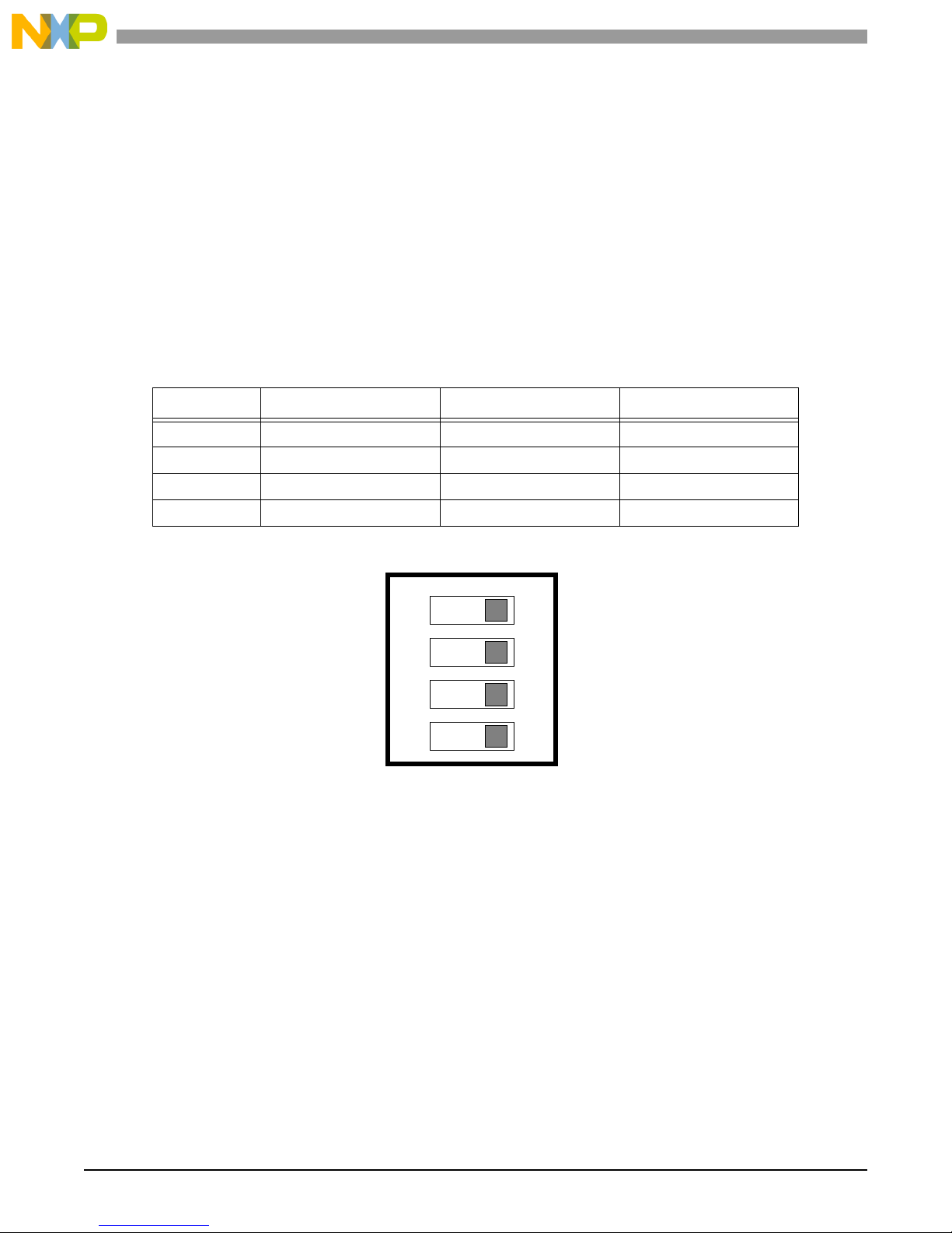
123 123
MII Mode
RMII Mode
Factory Default
2.4.6 MPC8272 Clock Mode Setting s (SW8)
Switch SW8 determines the clock sett ings for the MPC8272 processor. When a switch is in the ON position, its
related signal is deasserted to 0. When the switch is in the OFF position, its related signal is asserted to 1. For
details, refer to the MPC8272 PowerQUICC II™ Family Reference Manual. The default factory settings for the
MSC711xADS board are switc hes 1, 4, 6 = OFF and all other switches are ON.
• Switches 1–3 set MODCK[1–3], respectively.
• Switches 4–7 set MODCKH[0–3], respectively.
• Switch 8 sets the PCIMODCK bit.
Table 2-6. SW8 MPC8272 Clock Configuration
Switch SW8 OFF ON
1 MODCK1 1 0
2 MODCK2 1 0
3 MODCK3 1 0
4 MODCKH0 1 0
5 MODCKH1 1 0
6 MODCKH2 1 0
7 MODCKH3 1 0
8 PCIMODCK 1 0
2.4.7 Main Power Switch (SW9)
Switch 9 is the main power ON–OFF switch. Toggling the switch turns the main power ON (down) or OFF (up).
2.4.8 MSC711x Ethern et PHY MII/RM II Mode (JP1)
JP1 selects the connecti on mode of the Ethernet PHY connected to the MSC711x. The mode must be select ed
before power is turned on.
• In the MII (1-2) position, the PHY is in MII mode (factory default).
• In the RMII (2-3) position, the PHY is in RMII mode.
MSC711x Application Development System (MSC711xADS) Reference Manual, Rev. 1
Figure 2-5. JP1, MII Versus RMII Mode
Page 16

Hardware Configuration and Boot
12
12
Hard Reset Connected to Back Plane
Factory Default
Hard Reset Disconnected fr om Back Plane
JP2
123
123
TSI
External
Factory Default
JP3
123
123
External
Oscillator
Factory Default
JP4
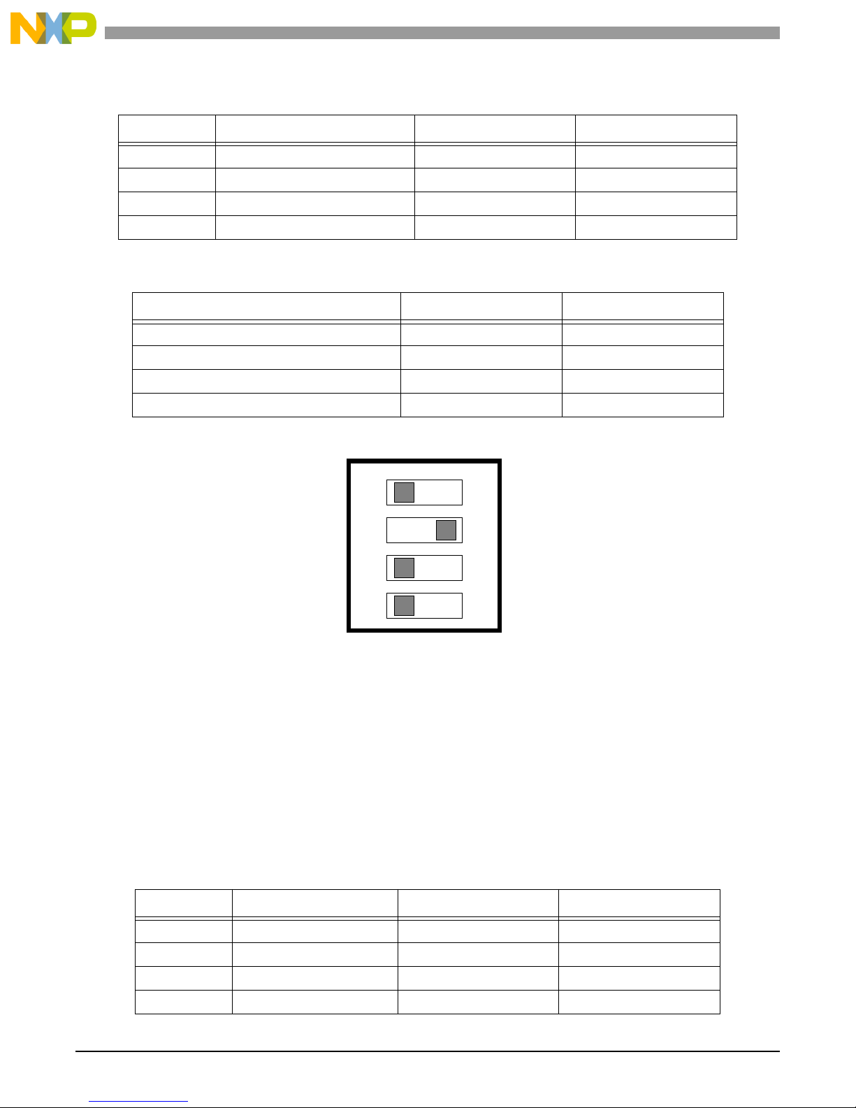
2.4.9 H.110 Back Plane Reset (JP2)
JP2 selects the connecti on of the MSC711x hard reset to the H.110 back plane.
• When placed, the MSC711x hard reset is connected to the H.110 back plane reset.
• When not placed, the MSC711x hard reset is disconnecte d from the H.110 back plane reset.
Figure 2-6. JP2, Hard Rest Back Plane
2.4.10 TD M Master Sel ecti on (JP3)
JP3 selects the master (clock and frame source) of the TDM channels of the MSC711x.
• In the TSI (1-2) position, the TSI is the TDM master (factor y default).
• In the external (2-3) position, the TSI frame and clock signals are disconnected from the MSC711x. The
MSC711x can be the TDM master or an external master (clock and frame sour ces) can be connected t hrough the
J5 edge connector.
Figure 2-7. JP3 , TSI TDM Master
2.4.11 MS C711x Clock In Source (JP4)
JP4 selects the source for the clock-in input of the MSC711x.
• In the external (1-2) position, the clock-in source is the SMB connector (P9) and the external clock generator
must be used.
• In the oscillator (2-3) posi tion, the clock-in source is the on-board oscillator (S2).
Note: For the mode change to occur, JP4 should be set while the board is powered OFF.
MSC711x Application Development System (MSC711xADS) Reference Manual, Rev. 1
Figure 2-8. JP4, Clock Input setting
Page 17

DIP-Switch and Jumper Settings
123
123
Flash
Factory Default
BSCR
JP5
123
123
Host and Slave Hard Resets
Factory Default
Connected to Each Other
Host and Slave Hard Resets
Not Connected to Each Other
JP6
2.4.12 MP C8272 Hard Reset Configuration Word Source (JP5)
JP5 selects the source for the Hard Rese t Configur ation Word (HRCW) of the MPC8272 processor.
• In the Flash (1-2) position, the HRCW is sourced from the Flas h memory.
• In the BCSR (2-3) position, the HRCW is sourced from the BCSR.
Figure 2-9. JP5, HRCW Setting
2.4.13 MP C8272 Hard Reset to MSC711x Hard Reset (JP6)
JP6 selects the connecti on of the MPC8272 hard res et to the MSC711x hard reset. When the two hard resets are
connected and an MPC8272 hard reset is generated, an MSC711x hard reset is also gener ated. The hard reset
generation works in only one dire ction. An MSC711x hard reset does not genera te a hard reset to the MPC8272
processor. When the hard resets are disconnected, the MPC8272 and the MSC711x pro cessors have separate hard
reset signals that do not affect each o ther.
• In the normal (1-2) position, the MPC8272 hard rese t is connected to the MSC711x hard reset.
• In the test (2-3) position, the MPC8272 hard reset is disc onnected from the MSC711x hard reset (factory default)
Figure 2-10. JP6, Hard Resets
2.4.14 PCI Expansion Enable/Disable (JP7)
JP7 switches between the PCI host bus and the MPC8272 60x bus (and HDI) visibility on the J1 and J2 edge
connectors.
• In the enable (1-2) p osition, t he MPC8272 PCI host b us is vi sible on th e J1 and J2 edge conne ctors, t hus enabl ing
the insertion of the board into a cPCI rack.
• In the disable (2-3) position, the MPC8272 60x (and HDI) bus is visible on J1 and J2 edge connectors.
MSC711x Application Development System (MSC711xADS) Reference Manual, Rev. 1
Page 18

Hardware Configuration and Boot
JP7
123
Enable
123
Disable
Factory Default
123
Enable
123
Disable
Factory Default
JP8
Figure 2-11. JP7, PCI Enable/Disable
2.4.15 Host (MPC8272) Enable/Disable (JP8)
JP8 enables and disables the host (MPC8272). When enabled, the MPC8272 is connected to the MSC711x . When
disabled, the MSC711x operates in stand-alone mode, regardless of the MPC8272 state.
• In the enable (1-2) position, the MPC8272 is enabled and connected to the MSC711x.
• In the disabled (2-3) positio n, the state of the MPC8272 does not influ ence the MSC711x, whic h therefor e works
independently in stand-a lone mode.
Note: The Disable mode is not yet supported. As a work around, disconnecting the MPC8272
HRESET signal from the MSC711x HRESET signal yields the same results. That is, the
MSC711x work independently of the MPC8272 state .
2.5 MSC711xA DS Boot
MSC711x device s can boot from the HDI16 bus or from an external EEPROM with a serial I2C interface. The
MSC711xADS uses a seri al EEPROM with a 256 Kb capacity (for example, M24256-B from Tmicroelectronic s
Co.1). The EEPROM memory is organized as eight 32 KB rows. This device can perform a hardware-based writeprotect of its memory map, and it is equipped with a soc ket so that it can be reprogrammed by an external
programmer. A PLD provides an optional connection to the host PC, which allows the user to reprogram the onboard boot EEPROM. At reset, the address of the I2C EEPROM is set to 000. The external pins of the I2C
EEPROM are described in
green LEDs.
1. Other devices that can be used are Microchip 24LC256, ATMEL AT24C256, or CATALYST CAT24WC256.
MSC711x Application Development System (MSC711xADS) Reference Manual, Rev. 1
Figure 2-13 and Table 2-7. The state of the SCL and SDA lines is indicated by red and
Figure 2-12. JP8, Host Enable
Page 19

Figure 2-13. I2C EEPROM Pins
3
V
CC
SDA
E[0–2]
SCL
WC
V
SS
Table 2-7. I2C EEPROM Pins
Pin Description
E0, E1, E2 Chip enable
SDA Serial data
MSC711xADS Boot
SCL Serial clock
WC Write control
V
CC
V
SS
Supply voltage
Ground
The I2C EEPROM is compatible with the I2C memory protocol, which defines a two-wire se rial interface with a
bidirectiona l data bus and serial clock. The memory carries a 4-bit unique device type identifier code (0b1010) in
accordance with the I2C bus definition. The I2C bus is connected to a header with two te st points, and its c lock r uns
2
at 400 KHz. The I
C EEPROM behaves as a slave device according to the I2C protocol, with all memory
operations synchronized by the serial clock. Read and write operations are initiated by a START condition, which
is generated by the bus master. The START condition is followed by a device select code and RW bit (see
Figure 2-14). It is terminated by an acknowledge bit that is inserted by the memory immediately after the 8-bit
transmission of the bus master, thus comprising a 9th bit. When the bus maste r read s the d at a, it ackno w led g es the
receipt of the data byte by placing an acknowledge 9
th
bit into the transmission stre am. Dat a tra nsfers are
terminated by a STOP condition after an Ack for WRITE, and after a No Ack for READ.
.
Device Type Identifier Chip Enable RW
7 6 5 4 3 2 1 0
Device Select Code
Note: The most significant bit, 7, is sent first.
1 0 1 0 0 0 0 RW
MSC711x Application Development System (MSC711xADS) Reference Manual, Rev. 1
Figure 2-14. Device Select Code
Page 20

Hardware Configuration and Boot
2.6 Board Contr ol s an d In dica tors
This section acquaints you with ope rational features of the MSC711xADS.
2.6.1 Abort and Reset Control
Table 2-8 describes the MSC711xADS abort and reset features.
Table 2-8. Abort and Reset Push Button Switches
Switch Name Description
SW1 MSC711x abort (NMI) Aborts progr am executi on by issui ng a level 0 inter rupt t o the MSC711x.
The ABORT switch signal is debounced
SW2 MSC711x hard reset
SW3 Power- o n reset Performs a power-on reset to the MPC8272 and to the MSC711x; all
SW10 MPC8272 soft reset Generates a soft reset to the MPC8272. The soft reset switch signal is
SW11 MPC8272 hard reset Generates a hard res et t o the MPC8272. A hard reset to the MPC8272
SW12 MPC8272 abort (NMI)
Generates a hard reset to the MSC711x but does not affect the host.
The hard reset signal is debounced.
configurat ion and all data residing in volatile memories are lost .
debounced.
also generates a hard reset to the MSC711x if JP6 is configured
accordingly (see
Hard Reset (JP6), on page 17). The HRESET switch signal is
debounced.
Aborts progr am exec ution by issuing a l eve l 0 int errupt to the MPC82 72.
The ABORT switch signal is debounced.
Section 2.4.13, MPC8272 Hard Reset to MSC711x
2.6.2 MSC711xADS Voltage Measurement
Table 2-9 describes MSC711xADS voltage measure ment.
CAUTION: The job of removing JS5, JS8, and JS6 and soldering the current meter
connections instead is very delicate and should be done by a skilled technician. If
this process is done by unskilled hands or repeated more than 3 times, permanent
damage may occur to the MSC711xADS.
Table 2-9. MSC711xADS Voltage Measurement
Name Description
JS5 Core voltage measurement JS5 resides in MSC711x main core current flow. To measure core
JS8 MSC711x I/O voltage
measurement
JS6 MSC711x PLL voltage
measurement
MSC711x Application Development System (MSC711xADS) Reference Manual, Rev. 1
current, JS5 should be removed with a solder tool and a cur rent meter
should be connected instead with wires as shor t and t hick as possible.
JS8 resides in th e MSC71 1x ma in I /O current flow. To measure I/O
current, JS8 should be removed with a solder tool, and a current meter
should be connected, with wires as short and thick as possible.
JS6 resides in MSC711x main PLL current flow. To measure PLL
current, JS6 should be removed with a solder tool, and a current meter
should be connected instead, with wires as short and thick as possible.
Page 21

Board Controls and Indicators
2.6.3 GND Bridges
There are seve n GND bridges on the MSC711xADS. These bridges assist you in taking general meas urements and
establishing logic-analyzer connections.
CAUTION: Shortening power connection to ground may result in permanent damage to the
MSC711xADS hardware. To prevent this condition, always use insulated ground
clips to connect to a ground bridge.
2.6.4 LED Indicators
Table 2-10 lists th e MSC 711 xADS LE D in di c ator s.
Table 2-10. LED Indicators
LED Indication Description
LD11 12 V Green. Indicates whet her the +12 V power supply is on.
LD10 5 V Green. Indicat es whether the +5 V power supply is on.
LD29 3.3 V Green. Indicates whether t he +3.3 V power supply is on.
LD9 2.5 V Green. Indicates whether the +2.5 V power supply is on.
LD13 1.5 V Green. Indicates whether t he +1.5 V power supply is on.
LD12 1.2 V Green. Presence of the +1.2 V power supply is on.
LD18 RUN Green. The MPC8272 is performing cycles on the PowerPC bus. When thi s LED
is dark, the MPC8272 i s eit her running internall y or stuck.
LD19 MPC8272 fast Ethernet
port enabled
LD1 MSC711x fast Ethernet
port enabled
LD2 MPC8272 RS-232 port ONYellow. The RS-232 transceiver connected to P16 is active and communicating.
LD3 MSC711x RS232 Port
ON
LD28 MPC8272 fast Ethernet
port full duplex
LD27 MPC8272 fast Ethernet
port 100Base-Tx
LD14 MSC711x fast Ethernet
port full duplex
Yellow. The fast Ethe rnet port PHY, the DM9161, is connected to FCC2. When
this LED is not lit, the DM916 1 is i n power-down mode and is disconnected from
FCC2. BCSR0 (see
controls the stat e of LD19.
Yellow. The fast Ethe rnet port PHY, the DM9161, is connected to t he MS C7 11x.
When this LED i s not l it, the DM9161 i s in power -down mode an d i s disco nnected
from the MS C711x, e nablin g the us e of its associ ated M II p ins f or oth er func tions .
BCSR2 (see
controls the stat e of LD1.
When this LED is not lit, the transceiver is in shut-down mode.
Yellow. The RS-232 transceiver connected to P7 is active and communicating.
When this LED is not lit, the transceiver is in shut-down mode.
Red. Indicates whether the DM9161 on the MPC8272 processor is enabled and
is operating in full-duplex mode.
Green. Indicates whether t he DM9161 on the MPC8272 processor is enabled
and is operating in 100 Mbps mode.
Red. Indicates whether the DM9161 on the MSC711x processor is enabled and
is operating in Full Duplex operation mode.
Chapter 4, Memory Map/Programming Model, on page 29)
Chapter 4, Memory Map/Programmin g Mode l, on page 29)
LD15 MSC711x fast Ethernet
port 100Base-Tx
LD4 General-purpose LED 2 Red. A gener al-purpose LED that the user cont rols via BCSR0.
LD5 General-purpose LED 1 Green. A general-purpose LED that the user controls via BCSR0.
MSC711x Application Development System (MSC711xADS) Reference Manual, Rev. 1
Green. Indicates whether th e DM9161 on the MSC711x processor is enabled
and is operating in 100 Mbps mode.
Page 22

Hardware Configuration and Boot
Table 2-10. LED Indicators (Continued)
LED Indication Description
LD6 MSC711x MII/TDM2
enable
LD7 MSC711x MII enable Green. The MSC7 11x M II /TDM2 port is connected to the Ethernet PHY in MII
LD8 MSC711x TDM2 enable Green. The MSC711x MII/TDM2 port is connected to the TSI and/or Ethernet
LD22 Parallel port connec tion in
SPP mode
LD21 Parallel port connec tion in
EPP mode
LD24 External debugger
connection
LD23 I2C EEPROM MSC711x
connection
LD20 I2C EEPROM parallel
port connection
LD17 Debug mode Green. Indic ates whether the MSC711x is forced into Debug mode using SW4-1
Green. Indicates whether t he MSC711x MII/TDM port is connected to the TDM
device/Ethernet PHY.
mode.
PHY in RMII mode.
Green. The board is connected directly to the PC parall el por t in SPP mode and
the COP/JTAG connector (P14) is irrelevant.
Green. The board is connected directly to the PC parall el por t in EPP Mode and
the COP/JTAG connector (P14) is irrelevant.
Green. A command conver ter can be connected to the COP/JTAG connector
(P14).
Green. The MSC711x is connected to the I2C EEPROM.
Green. The parall el port is connected to the I2C EEPROM.
(see
Section 2.4.2, MSC711x Power-Up Settings (SW4), on page 12).
MSC711x Application Development System (MSC711xADS) Reference Manual, Rev. 1
Page 23

Reset
Board-Level Functions 3
This chapter discusses reset, clock, and powe r supply.
3.1 Reset
There are several reset sources on the MSC711XADS:
• Power-on reset for both the MSC711x and MPC8272 processors (PORESET).
• Manual hard reset for both the MSC711x and MPC8272 processors (HRESET).
• Manual soft reset for the MPC8272 processor (SRESET).
• MPC8272 internal sources (see also the MPC8272 PowerQUICC II™ Family Reference Manual).
• MSC711x internal sources (see also the MSC711x Reference Manual).
3.1.1 Power-On Reset
The power-on reset to the MPC8272 and MSC711x initializes the processor states after power-up. A dedicated
logic unit a sserts
different voltage regulator. Power-on reset is either generated manually or by an on-board push button (SW3).
At the end of power-on reset, the MPC8272 samples the MODCK[1–3] bits to configure its various clock modes
(core, CPM, bus, PCI, and so on). The MODCK[1–3] combination options are selected by means of dip switches,
as described in
After deassertion of power- on reset, the hard-reset sequence starts. During the hard-reset sequence, many options
are configured. Some of these option s are additiona l clock configu ratio n bits in MODCKH[0–3]. These bits are the
most significant bit s of the MODCK field, whic h determine additional options for the clock generator. Although
these bits are sampled when the hard reset sequence is entered, they are influential only once: immediate ly after
power-on reset. If a hard reset sequence is entered later, MODCKH[0–3] are sampled but no action is taken.
The PCI_MODCK signal is sampled concurrently with the MODCK[0–3] bits and determines the PCI bus clock
frequency. When it is asserted high, it divides the PCI bus frequency by two. When it is asserted low, the PCI bus
frequency is as determined by the MODCK[1–3] and MODCKH[0–3] signals.
At the rising edge of the powe r- on signal , the MSC711x processor samples four pins to det ermine its configur atio n.
Those pins are
deasserted.
PORESET input long enough stabilize the MSC711x and MPC8272 core voltages, powered by a
Section 2.4.6, MPC8272 Clock Mode Settings (SW8), on page 15.
BM0, BM1, SWTE, and HDPOL. These pins are sampled only once immediately after PORESET is
3.1.2 Hard Reset
Any one of the following sources can generate a hard reset on the MSC711xADS:
• COP/JTAG port. Asserting the HRESET line connected to the COP/JTAG port connector dir ectly generates a
hard-reset for both the MPC8272 and MSC71 1x devices, depending on the JP6 position.
MSC711x Application Development System (MSC711xADS) Reference Manual, Rev. 1
Page 24

Board-Level Functions
CLK GEN
100 MHz
60x SDRAM
Expansion
Mictor
Low
Skew
Buffers
• OCE10/JTAG port. Asserting the HRESET line connected to the OCE10/JTAG port connector directly generates
a hard reset for onl y the MSC711x processo r.
• Manual hard reset. Both the MPC8272 and the MSC711x processors have their own HRESET push button. In
addition, you can generate a manual hard reset for the MSC711x by toggling a bit in BCSR3.
• Internal sources. Both the MSC711x and MPC8272 have internal sources that can generate an HRESET in
response t o speci fic ev en ts .
A hard reset causes the MPC8272 and MSC71 1x processors to reset all their internal hardware except for PLL
logic and reacquires the hard-r eset configuration from its current source (for the MPC8272). Since hard reset also
resets the refresh logic fo r dynamic RAMs, the ir content is lost as well. The MPC8272
HRESET to the MSC711x processor, depending on the JP6 position. The MSC711x HRESET affects only the
MSC711x and does not generate an MPC8272
HRESET.
HRESET can generate an
CAUTION: Contention on the HRESET may cause permanent damage to either board logic
and/or to the MPC8272 and the MSC711x processors. To prevent contention,
always d rive HRESET with an open-drain gate.
When a hard reset is applied to the MPC8272 (externally as well as internally), it samples the Hard Reset
Configuration Word (HRCW). This configuration word can be taken from the Flash memory or BCSR (the most
significant 8 bits of the dat a bus), depending on the JP5 position.
3.2 Clocking
There are three main clock circuits on the MSC711xADS board:
• MPC8272 system clock
•PCI clock
• MSC711x system clock
3.2.1 MPC8272 System Clock
The MPC8272 requires a single clock sourc e as the main cloc k source. All MPC8272 60x bus timings are
referenced t o the main clock input,
with internal sk ew eli minati on via a PLL. A 100 MHz 3.3 V clock oscilla tor i s conne cted to a low inte r- skew buf f er
(U10) to split the load be tween all clock consumers on both boards. To provide a clean clock input for proper
operation, special care is taken to isolate and terminate the clock ro ute between the on-board PLL and the
MPC8272. The main clock scheme is shown in Figure 3-1.
CLKIN1. The timing ratio between the main clock input and the bus clock is 1:1,
MSC711x Application Development System (MSC711xADS) Reference Manual, Rev. 1
Figure 3-1. Main Clock Generator Scheme
Page 25

Clocking
PCI Device 1
PCI Device 2
PCI Device 3
OUT1
OUT2
OUT3
OUT4
IN
Low Skew Clock Buffer
MPC8272
DLLOUT
CLKIN1
CLKIN2
Clock Generator
100 MHz
3.2.2 PCI Clock
The PCI bus clock is derived internally from the main clock input, CLKIN1. The generated PCI clock is output from
a PCI-dedicat e d PLL (named DLL). T hat clo ck outp ut feed s an on- b oard low-s k ew an d fast clo ck dist rib uto r tha t
distributes the PCI cloc k to all on-board PCI devices. One of the outputs is fed back to the PCI clock in the
MPC8272 via the
driven to the DLL, which synchronizes the DLL output clock to t he
skew between the DLL out put and
and low skew , all copper traces are careful ly kept from the clock distributor outputs at the same lengths, including
the output that is fed ba ck to
CLKIN2 input. All PCI bus timings are referenced to the CLKIN2 input clock. This clock input is
CLKIN2 input clock and ther eby maintains low
CLKIN2 input. To comply with the PCI standa rd and achie ve bus s ynchro nization
CLKIN2.
3.2.3 MSC711x System Clock
The MSC711x processor requires a reference clock input (CLKIN) by which the clock synthesis module in the
MSC711x core gener at es all the tim i ngs n eeded . The rec o mm en d ed
shows, the clock synthesis module is composed of the following blocks:
• Phase lock loop (PLL) with associated multipliers and dividers
• AHB/APB bus clock divider
• Timer clock multiplex
• Wake-up control
• Control registers
Together, these blocks generate the following clock signals for core and periphe ral clocking:
• External input clock. provides a reference clock for the system.
• Core cl ock. Obtained by a predivision of the input clock and multiplying the frequency in the PLL.
• AHB clo ck. Generated similarly to the core clock but with an additional division stage.
• IPBus clock. Generated from the AHB clock.
• APB clock. Generated from the AHB clock.
• Timer c lock. Can be derived from the external input clock or from the SkyBlue clock.
The control register is use d for programming the clock synthesis module. The wake-up con trol block wakes the
processor out of its low-power modes.
MSC711x Application Development System (MSC711xADS) Reference Manual, Rev. 1
Figure 3-2. PCI Clock Generator Scheme
CLKIN frequency is 20 MHz. As Figure 3-3
Page 26

Board-Level Functions
Watchdog Timer
1
Device Resources
Timers
Timer Module
DSP Extended Core
Input
Clock
Time r C lock
4
1
Clocks can be disabled in Stop mode. Disables PLL, core clock, ECore clock, AHB clock, IPBus clock, and
2
Clocks can be disabled at this point in Stop mode. Disables ECore clock, AHB clock, IPBus clock, and APB clock.
3
Clocks are disabled at this point in Wait and Stop modes. Disables the ECore clock.
4
Clocks can be disabled at this point in Stop mode. Disables the input clock used in timer clock generation.
HLTACK
32-bit
IPBus
CLKIN
AHB Clock
to Crossbar Switch, DMA,
to 32-Bit W atchdog Timer
TDM Peripheral
to TDM Clock, Frame Sync
EVNT
Event
Port
MUX
MUX
UART
to UART Tx, R x
M2, Boot ROM
CPU
3
SC1400 Core
DIV
(/1 to /25)
MULT
(x1 to x28)
PLL
MUX
CLKOUT
Wake-up
Control
APB Clock
CLKO
IPBus Clock / 2
Timer C lock / 2
/24 /1 to /216
MUX
External Memory Interface
to External. Memo ry. Contro ller
to DDR Clock Pins
Clock Synthesis
Module
Time r B
Outputs
Timer A
Outputs
Debug
Port
I2C
to Serial
MUX
/22, ..., /3 8 40
Ethernet MAC
to Ethernet MAC
/2, /4,... /1 2 6
MDC
AHB
Clock
RX_CLK
TX_CLK
5
Clocks can be disabled at th is point in Stop mode. Disables the watchdog timer clock.
IPBus Clock
AHB DIV
(/2)
2
ECore clock
Core Clock
DDR Clock
6
HLTREQ
STOPCTL
CLKCTL
5
Watchdog Clock
/2
6
Clocks can be disabled at this point i n Stop mode. Disables the DDR clock.
AHB
Clock
IPBus
Clock
/2
/26
Timer
Bit C lock
Generator
Clock
APB Clock.
Figure 3-3. MSC711xADS Timing System
MSC711x Application Development System (MSC711xADS) Reference Manual, Rev. 1
Page 27

3.3 Power Su ppl y
The MSC711xADS uses the fol lowing voltages:
• 5 V: (Comm an d converter).
• 3.3 V: (MSC711x and MPC8272 I/O and for most of the components)
• 2.5 V: (SSTL components: the DDR chip and the DDR interface in the MSC711xADS).
Power Supply
•V
: (1.25 V for DDR active terminat i on ).
REF
• 1.5 V: MPC8272 core voltage.
• 1.2 V: MSC711x core voltage.
These voltages are derived from the 12 V main power supply (switch P23).
The MSC711xADS maximum currents demands are:
• 100 mA for the I/O at 3.3 V.
• 240 mA for the SSTL_IO +DDR at 2.5 V.
• 511 mA for the core at 1.2 V.
The MSC711xADS has three distinct power supplies (1.2 V core, 2.5 V DDR I/O, and 3.3V standard I/O). When
the board is powered up or powered down, the following se quences of operations must be followed.
The power-up sequen ce is as follows:
1. Turn on the highest supply ( 3.3 V sta ndard I/O).
2. Turn on the 2.5 V DDR I/O supply.
3. Turn on the lowest supply (1 .2 V core).
The power-down sequen ce is as follows:
1. Turn off lowe st supply (1.2 V core).
2. Turn off 2.5 V DDR IO.
3. Turn off highe st supply last, 3.3 V standard I/O.
CAUTION: Latch up forward bi asing of ESD devices and e xcessive c urrents ca n lead to severe
device damage. To avoid this problem, a proper power-up and power-down
sequence at the board level must performed.
MSC711x Application Development System (MSC711xADS) Reference Manual, Rev. 1
Page 28

Board-Level Functions
Time
Voltage
R
a
m
p
-
U
p
R
a
m
p
-
D
o
w
n
(VIO)t 3.3 V
(VSSTL)t 2.5 V
(VCORE)t 1.2 V
Voltage Differen ce
Must Be > 0.7V
LDO
12 V to 5 V
DC 2 DC
12 V to 3.3 V
10A Max
LDO 2.5 V
LDO 1.5 V
VTT 1.25 V
LDO 1.2 V
3.3 V
2.5 V
1.5 V
Power
Sequence
1.2 V
1.25 V
5 V
3.3 V 10A
Power Up Reset
Figure 3-4. MSC711xADS Power Up/Powe r Down Sequence
From a time variant viewpoint, when power is ramped up or down, the 2.5 V supply must at any instant maintain a
voltage that is at least 0.7 V less than that of the 3.3 V supply . Also, at any instant, the 1.2 V supply must maintain
a voltage that is at least 0.7 V less than that of the 2.5 V supply.
MSC711x Application Development System (MSC711xADS) Reference Manual, Rev. 1
Figure 3-5. Power Supply Block Diagram
Page 29

Memory Map
Memory Map/Programming Model 4
This chapter presents a recommended memory map and describes the MSC711xADS registers in detail. The
MPC8272 memory controller is use d as a chip-se lect gener ator to access on-boar d (and exter nal) memories , saving
board area and reducing cost and power consumption while increasing flexibility. When a
buffered memory is disa bled via the BCSR, the local data transceivers are disabled during access to that region to
prevent possible contention on data lines. Table 3-1 shows the MPC8272 chip-select assignments to the various
memories/registers on the MSC711xADS.
Table 3-1. MPC8272 Chip-select Assignments
Chip Select Assignment Bus
CS0 Flash memory 60x (buffered)
CS1 BCSR 60x (buffered)
CS region assigned to a
CS2 SDRAM 60x (main)
CS3 PMC E1/T1 framer (via the BCSR) 60x (buffered)
CS4 PEF20451 TSI switch (via the BCSR) 60x (buffered)
CS5 SLIC-SLAC MPI (via the BCSR) 60x (buffered)
CS6 HDI CS0 60x (buffered)
CS7 HDI CS1 60x (buffered)
4.1 Memory Map
All accesses to the MPC8272 memory slaves are controlled by the MPC8272 memory controller. Therefore, the
memory map is reprogrammable. After a hard reset, the debugger checks for the size, delay, and type of the Flash
memory on the board and programs the memory controlle r accordingly. The SDRAM and the Flash memory
respond to all types of memory access; tha t is, problem /supervisory, program/data, and DMA. The memory map
shown in
map, according to your needs.
0x00000000–0x03FFFFFF 60x SDRAM 64 bit 64 MB
Table 3-2 is a recommended memory map. However, the devices addresses can be moved aroun d the
Table 3-2. Memory Map
Address Range Memory Type Port Size Memory Size
0x04000000–0x044FFFFF Empty Space 5 MB
MSC711x Application Development System (MSC711xADS) Reference Manual, Rev. 1
Page 30

Memory Map/Programming Model
Address Range Memory Type Port Size Memory Size
Table 3-2. M em ory Map (Continued)
0x04500000–0x04507FFF
0x04500000
0x04500004
0x04500008
0x0450000C
0x04500010
0x04500014
0x04500018
0x0450001C
0x04508000–0x045FFFFF Empty space 1 MB
0x04600000–0x04607FFF E1/T1 Framer 8 Bits 32 KB
0x04608000–0x0460FFFF SLIC/SLAC 32 Bits 32 KB
0x04610000–0x04617FFFF TSI 8 Bits 32 KB
0x04700000–0x0471FFFF MPC8272 internal map 32 Bits 128 KB
0x04720000–0x04727FFFF HDI CS1 16 Bits 32 KB
0x04728000–0x0472FFFF HD I CS2 16 Bits 32 KB
0x04730000–0x047FFFFF Empty space ~800 MB
0x04800000–0x04FFFFFF PCI memory agent PIMMR 32 Bits ~5 MB
0x05000000–0x7FFFFFFF Empty space ~2 GB
0x80000000–0xBFFFFFFF PCI memory GPL windows 32 Bits 1 GB
BCSR[0–7]
BCSR0
BCSR1
BCSR2
BCSR3
BCSR4
BCSR5
BCSR6
BCSR7
32 Bits 32 KB
4 Bytes
4 Bytes
4 Bytes
4 Bytes
4 Bytes
4 Bytes
4 Bytes
4 Bytes
0xC0000000–0xFF7FFFFF Empty space ~240 MB
0xFF800000–0xFFFFFFFF Flash 16 Bits 8 MB
4.2 Board Contr ol and St at us R egiste rs (BC SRx )
Most hardware option s on the MSC711xADS are cont rolled or monitored by the BCSR, whic h is a 32-bit wide set
of read/write regis ters. The BCSR is accessed via the MPC8272 memory controller and includes registers
BCSR[0– 7]. Since the minimum block size for a chip select region is 32 KB and only three lines, A[27–29], are
decoded by the BCSR for register selection, BCSR[0–7] are duplicated inside that region.
MSC711x Application Development System (MSC711xADS) Reference Manual, Rev. 1
Page 31

Board Control and Status Registers (BCSRx)
BCSR0 Board Control Status Register 0 Offset 0x0
Bit 0 1 2 3 4 5 6 7 8 9 10 11 12 13 14 15
PQETHENPQETH
TYPE R/W R R/W R
RESET 0 1 1 1 1 0 1 1
Bit 16 17 18 19 20 21 22 23 24 25 26 27 28 29 30 31
TYPE R
RESET 0 0 0 0 0 0 0 0 0 0 0 0 0 0 0 0
PQRSENCONFEN Bootp — GPLLED0 GPLLED1 —
RST
—
BCSR0 is accessed at offset 0x0 from the BCSR base address. BCSR0 gets its defaults at power-on rese t.
Table 4-1. BCSR0 Bit Descriptions
Bit Reset Value Description Settings
PQETHEN
0
PQETHRST
1
0 MPC8272 Ethernet enable. 0 Disabled.
1 Enabled.
1 MPC8272 Ethernet reset. 1 Deasserted.
0 Asserted.
PQRSEN
2
CONFEN
3
Bootp
4
5 Reserved. Write to zero for future compatibility.
GPLLED0
6
GPLLED1
7
—
8–31
1 MPC8272 RS-232 transceive r enabl e. 1 Disabled.
1 MPC8272 Hard Reset Configurati on Word
source.
1 Flash boot sector write protect: 0 Protect.
1 General-purpose LED 0. 0 ON.
1 General-purpose LED 1. 0ON.
Reserved. Write to zero for future compatibility.
0 Enabled.
0 Flash memory.
1 BCSR.
1 Do not protect.
1 OFF.
1 OFF.
MSC711x Application Development System (MSC711xADS) Reference Manual, Rev. 1
Page 32

Memory Map/Programming Model
BCSR1 Board Control Status Register 1 Offset 0x4
Bit 0 1 2 3 4 5 6 7 8 9 10 11 12 13 14 15
BVER0 BVER1 PCIEN PCIM66E PCIINTA PCIINTBPCIINTCPCIINTD
TYPE R
RESET 0
Bit 16 17 18 19 20 21 22 23 24 25 26 27 28 29 30 31
TYPE R
RESET 0
BCSR1 can be read at any time, and it gets its defaults at power-on reset.
Table 4-2. BCSR1 Bit Descriptions
Bit Reset Value Description Settings
BVER0
0
BVER1
1
PCIEN
2
PCIM66E
3
PCIINTA
4
PCIINTB
5
PCIINTC
6
PCIINTD
7
—
8–31
0 Board version 0. 00 Prototype.
01 Pilot.
10 Rev. A.
11 Rev. B.
0 Board version 1.
0 PCI enable (HDI disable). 0 PCI connection enable.
1 60x (HDI) connection enabled.
0 PCI 66 MHz enable. 0 PCI bus is working at 66 MHz.
1 PCI bus is working at 33 MHz.
0 PCI inte rrupt A. 0 Interrupt.
1 No interrupt.
0 PCI inte rrupt B. 0 Interrupt.
1 No interrupt.
0 PCI inte rrupt C. 0 Interrupt.
1 No interrupt.
0 PCI inte rrupt D. 0 Interrupt.
1 No interrupt.
0 Reserved . Wri te t o zer o for future com pa tibility.
MSC711x Application Development System (MSC711xADS) Reference Manual, Rev. 1
Page 33

Board Control and Status Registers (BCSRx)
BCSR2 Board Control Status Register 2 Offset 0x8
Bit 0 1 2 3 4 5 6 7 8 9 10 11 12 13 14 15
H8B DBREQ BM0
TYPE R R/W R
RESET 0 1 1 0
Bit 16 17 18 19 20 21 22 23 24 25 26 27 28 29 30 31
TYPE R
RESET 0
BM1
SWTE
HDSPOL
HDDS PQDMA
—
—
BCSR2 is a read-only status regis ter. It can be read at any time.
Table 4-3. BCRS2 Bit Descriptions
Bit Res et Val ue Description Setting
H8B
0
DBREQ
1
BM0
2
BM1
3
0 MSC711xADS HDI 8-Bit mode. 0 16-bit HD I m o de.
1 8-bit HDI mode.
0 MSC711xADS debug mode request. 0 Normal run mode.
1 Debug mode.
0 MSC711xADS boot mo de 0–1. 00 HDI.
01 I2C.
0
SWTE
4
HDSPOL
5
HDDS
6
PQDMA
7
—
8–31
0 MSC711xADS sof tware watchdog. 0 Watchdog disable.
1 Watchdog enable.
0 MSC711xADS HDI strobe polarity. 0 Active low.
1 Active high.
1
1 MPC8272 DMA DREQ3 si gnal value ac cording to
0
MSC711x Application Development System (MSC711xADS) Reference Manual, Rev. 1
MSC711xADS HDI double data strobe.
PQDMA.
Reserved. Write to zero for future compatibility.
0 Single strobe.
1 Double strobe.
•PQDMA = 0 → DREQ3 =
HRRQ.
•PQDMA = 1 → DREQ3 = HRRQ
and
CS6.
Page 34

Memory Map/Programming Model
BCSR3 Board Control Status Register 3 Offset 0xC
Bit 0 1 2 3 4 5 6 7 8 9 10 11 12 13 14 15
SLETHEN MIITDM2EN MIIEN SLUARTEN
TYPE R/W R
RESET 0 0 0 0 0 0 1 0 0
Bit 16 17 18 19 20 21 22 23 24 25 26 27 28 29 30 31
TYPE R
RESET 0
I2CEN
SLI2CEN
SLHreset HOSTEN
—
BCSR3 can be read or written at any time.
Table 4-4. BCSR3 Bit Descriptions
Bit Reset Value Description Settings
SLETHEN
0
MIITDM2EN
1
MIIEN
2
SLUARTEN
3
0 MSC711x fast Ethernet port enable. 1 Enable.
0 Disable
0 MSC711xADS MII/TDM2 port . 0 MII/TDM2 enable.
1 MII/TDM2 disable.
0 MSC711xADS MII/TDM2 port multiplex. 0 MII enable.
1 RMII/TDM2 enable.
0 MSC711xADS UART transcei ver (RS-232). 0 Enable.
1 Disable
I2CEN
4
SLI2CEN
5
SLHreset
6
HOSTEN
7
—
8–31
0 I2C EEPROM bus enable. 0 Enable.
1 Disable.
0 I2C EEPROM connection. 0 MSC711xADS
1 Parallel port.
1 MSC711x hard reset generation. 0 Asserted
1 Deasserted.
0 MPC8272 enabled as host. 0 Enable.
1 Disable.
0 Reserved. Write to zero for future compatibility.
MSC711x Application Development System (MSC711xADS) Reference Manual, Rev. 1
Page 35

Board Control and Status Registers (BCSRx)
BCSR4 Board Control Status Register 4 Offset 0x10
Bit 0 1 2 3 4 5 6 7 8 9 10 11 12 13 14 15
SYSEN GA0 GA1 EVENT0
TYPE R
RESET 1
Bit 16 17 18 19 20 21 22 23 24 25 26 27 28 29 30 31
TYPE R
RESET 0 0 0 0 0 0 0 0 0 0 0 0 0 0 0 0
EVENT1
EVENT2
EVENT3 EVENT4
—
BCSR4 is a read-only register tha t can be read at any time.
Table 3-3. BCRS4 Bit Descriptions
Bit Reset Value Description Function
SYSEN
0
GA0
1
GA1
2
1 MSC711xADS is in cPCI rack: 0 System slot.
1 Slave slot or stand-alo ne.
cPCI rack geographical address 0.
cPCI rack geographical address 1.
EVENT0
3
EVENT1
4
EVENT2
5
EVENT3
6
EVENT4
7
—
8–31
MSC711xADS event 0 indication.
MSC711xADS event 1 indication.
MSC711xADS event 2 indication.
MSC711xADS event 3 indication.
MSC711xADS event 4 indication.
0 Reserved. Write to zero for future compatibil ity.
MSC711x Application Development System (MSC711xADS) Reference Manual, Rev. 1
Page 36

Memory Map/Programming Model
BCSR[5 – 7] Board Control Status Registers 5–7 Offset 0x14
BCSR[5–7] are accessed at offset 0x14 from the BCSR base address. They are read-only registers that can be read
at any time.
Table 3-4. BCRS (5–7) Bit Descriptions
Bit Reset Value Description Type
—
0–4
CPLD REV
5–7
—
8–31
11111 Reserved. R
000 CPLD code revision. R
0000
Reserved. R
0000
0000
0000
0000
0000
MSC711x Application Development System (MSC711xADS) Reference Manual, Rev. 1
Page 37

HDI16 Host Processor Interface
MSC711xADS Interfaces 5
This chapter describes the various interfaces of the MSC711xADS, including the host interface (HDI16), the
connection between the MSC711x and MPC8272 processors, RS-232 ports, OCE10/JT AG interface, Ethernet,
DDR SDRAM, Flash memory, time-slot interchanger, SLIC SLAC interface, and E1/T1 framer.
5.1 HDI16 Hos t P rocesso r Int er face
The host processor can be either the MPC8272 or an outside host, and it connects to the MSC711x proc essor
through the HDI16 host interf ace, which is a 16-bit wide, full-duplex, double -buffered parallel port that can
directly connect to the data bus of a host processor. The HDI16 port supports a variety of buses and gluele ssly
connects with a number of industry- standard microcomputers, micropr ocessors, and DSPs. The HDI16 host bus
can be asynchronously acce ssed, independently of the clocks on the DSP, because the HDI16 registers are divided
into two banks:
• External host register bank that is accessible to an external host.
• Chip regist er bank that is accessible to the MSC 7 11x d evic e.
The HDI16 supports two classes of inte rfaces to external devices:
• Host processor/microcont roller (MCU) connection interface.
• DMA controller interface.
5.1.1 HDI16 Configuration
On the MSC71 1x device , the HLEND bit i n the HPCR regis te r must al ways have a value of 0, whic h configur es the
HDI16 module for big-endian operation. This is the default value. The HDI16 port on the MSC71 1x differs from
the MSC8101 HDI16 port, as follows:
• Bits on the HD bus are numbered with bit 0 as the LSB.
• Bits on the HA bus are numbered with bit 0 as the LSB.
• Bits in HDI16 registers are numbered with bit 0 as the LSB.
• The Host Port Pin (HPE) does not exist as a pin on the MSC711x. Instead, this signal is internally tied as
asserted. That is, the host port is enabled. To disable this port, use the HEN bit in the HPCR register.
• HDSP pin value is sampled only at reset.
• H8BIT pin value is sampled only at reset.
• Host address bus uses only three pins HA[2–0]. The HA3 pin is not used, and it is internally deasserted to 0.
• The reset configuration registers are not accessible to an external host and are not supported.
MSC711x Application Development System (MSC711xADS) Reference Manual, Rev. 1
Page 38

MSC711xADS Interfaces
HDI
Header
MSC711x
HD[15–0]
HA[2–0 ], C S I*
HRW, HDS*
HRRQ*
Host Interface Connector
1
3
5
7
9
11
13
15
17
19
21
23
25
27
29
31
33
35
2
4
6
8
10
12
14
16
18
20
22
24
26
28
30
32
34
36
GND
HD0
HD2
HD4
HD6
HD8
HD10
HD12
HD14
GND
HA0
HA2
HCS1
HRRQACK
HRDRW
HRESET
3.3v
GND
GND
HD1
HD3
HD5
HD7
HD9
HD11
HD13
HD15
GND
HA1
HA2
HCS2
HREQ
HD5
PORST
NC
GND
5.1.2 HDI16 BUS Connection to the Host Processor Header
The host inte rface connector is a 36-pin, two-row header connector. The MSC711xADS board and the host board
are connected via a 36-line fl at cable.
Table 5-1 describes the connector pins.
Figure 5-1 shows the connecting signals and the pinout of the connector.
Figure 5-1. HDI16 Bus Connection to the Host Processor Header
MSC711x Application Development System (MSC711xADS) Reference Manual, Rev. 1
Page 39

HDI16 Host Processor Interface
Table 5-1. Host Interface Connector Pins
Pin Signal Name Attribute Description
1 GND P Digital GND. Main GND plane.
2
3 HD0 I/O Host interface bidirectional tri-stated data bus port: HD[0–15].
4 HD1
5 HD2
6 HD3
7 HD4
8 HD5
9 HD6
10 HD7
11 HD8
12 HD9
13 HD10
14 HD11
15 HD12
16 HD13
17 HD14
18 HD15
19 GND P Digital GND. Main GND plane.
20
21 HA0 I Host Interface Address Line HA[0–3].
22 HA1
23 HA2
24 HA3 — Not used. Reserved.
25 HCS1 I H ost Chip-Select 1.
26 HCS2 I H ost Chip-Select 2.
27 HACK I/O,T.S. Host Acknowledge or Receive Host Request Output.
28 HREQ Q,T,S H ost Request or Transmit Host Request Output.
Bit 0 corresponds to the LSB of the bus.
The HDI CS is determined by the logical OR between HCS 1 and HCS2.
The HDI CS is determined by the logical OR between HCS 1 and HCS2.
Host DMA Acknowledge/ Host Receive Request
When the HDI16 is program med to int erfac e to a sin gle host request , thi s pin is
the host acknowledge Schmitt trigger input in host DMA mode (HACK). The
polarity of the host DMA acknowledge is programmable.
When the HDI16 is program med to int erfac e to a sin gle host request , thi s pin is
the host request output ( HREQ). This pin can be used for host DMA requests
in host DMA mode.
29 HRW I Host Read/Write or Host Read Input.
MSC711x Application Development System (MSC711xADS) Reference Manual, Rev. 1
Page 40

MSC711xADS Interfaces
MPC8272 MSC711x
Buffer
BCSR
60x Bus D[0–15]
60x Bus A[28–30]
CS
R/W
BBCTL0
IDMA
60x Bus D[0–15]
60x Bus A[28-30]
BCS
HRW
HDS
HDDS
HREQ
HACK
HREQ
HACK
HDDS
HDS
HRW
CS
HD[15–0]
HA[2–0]
Table 5-1. Host Interface Connector Pins (Continued)
Pin Signal Name Attribute Description
HDS I Host Read/Write or Host Read Input.
30
HRESET I/O, P.U MSC7116 Hard Reset.
31
PORESET I/O, P.U Power-On-Reset.
32
3V3 P +3.3V Power Out. These lines are connected to the main 3.3 V plane of the
33
MSC711xEVM.
NC — Not connected.
34
GND P Digital GND. Main GND plane.
35
36
5.2 60x Bus B uf ferin g
For best MSC711xADS performance, the capacitive load over the 60x bus must be reduced as much as possible.
Therefore, the slower devices on the bus, such as the Flash memory, HDI interface, BCSR, and E1/T1 framer, are
buffered. The SDRAM is not buffered. To reduce noise and reflections further, serial damping resistors are placed
over SDRAM addresses and all MPC8272 strobe lines. The data transceivers are open only if there is an access to
a valid buffered boa rd address or during hard reset configuration. Data conflicts are avoided for unbuffered
memory reads or off-board memory reads, if they are not mapped to a va lid address on the board. It is the user’s
responsibili ty to prevent such errors.
5.3 MSC711x C onn ection to th e MPC82 72
Figure 5-2 s hows the data and sig nal con necti ons between the MSC71 1x de vice and the host (MPC8272). T he data
and address lines are buffered, but the control signals (re ad/write, acknowledge, and so on) are transferred via the
Board Control and Stat us Register (BCSR). For details on the BCSR, see
Model, on page 29.
MSC711x Application Development System (MSC711xADS) Reference Manual, Rev. 1
Figure 5-2. MSC711x Connec tion to the MPC8272
Chapt er 4, Memory Map/Programming
Page 41

RS-232 Ports
1
2
3
4
5
6
7
8
9
GND
NC
RX
TX
NC
NC
NC
NC
NC
Tx (O) Transmit Data
Rx (I) Receive Data
5.4 RS- 232 Ports
T wo RS-232 ports on the MSC711xADS board assist with the development of user applications and provide
convenient communica tion channe ls wit h a terminal or a host computer. One port connects to the MPC8272 via th e
MPC8272 SCC, and the second port connects to the MSC711x processor via the MSC711x UART. The RS-232
port for the MPC8272 is one 9-pin D-Type female connector. The connec tor should directly connect (via a flat
cable) to any IBM-PC compatible RS-232 port. The RS-232 connection for the MSC711x is a pin connection at
point P7.
5.4.1 RS-232 to MSC711x
The RS-232 connection to the MSC711x processor occurs via a MAX3241 transceiv er that generates the required
RS-232 levels using a single 3.3 V supply . The transceiver is always enabled. The RS-232 pins can be switched to
drive an expansion connect or.
Figure 5-3 shows the RS-232 port signals.
Figure 5-3. MSC711xADS RS-232 Serial Port Connections
5.4.2 RS-232 to MPC8272
The RS-232 to MPC8272 port connects to the SCC port on the MPC8272 device via a MAX3241 transcei ver tha t
generates the require d RS-232 levels using a single 3.3 V supply. The transceiver is al ways enabled. The RS-232
pins can be switched to drive an expa nsion connec tor. Figure 5-4 describes the RS-232 por t signals. The directions
I, O, and I/O are relative to the MSC711xADS board. For example, I means input to the MSC71 1xADS.
MSC711x Application Development System (MSC711xADS) Reference Manual, Rev. 1
Page 42

MSC711xADS Interfaces
1
2
3
4
5
6
7
8
9
GND
DTR
RX
TX
DCD
DSR
RTS
CTS
N.C.
14-Pin OCE10 Header
MSC711x
Device
JTAG
16-Pin JTAG Header
MPC8272
Device
JTAG
JTAG
Signals
I2C
TDO
TDI
TDO
JTAG Bus
TDI
SCI, SDA
Parallel Port
Voltage
Transceiver
PLD
Address
Latch,
Decoder,
And
I
2
C
Transceiver
JTAG
TAP
Master
74LVX161284
(Fairchild)
Altera
(Serie s 30 00)
SN74LVT8980A
(TI)
A[0–2]
D[0.7]
CTL
256 KB
Serial
EEPROM
M24256
Jumper
JTAG_EPP
JTAG_SERIAL
JTAG_ExtConv
I2C_PP
I2C_CPU
SCL, SDA
SCL
SCL
Write
Protect
I2C
• DCD (O). Data Carrier Detect. This line i s always asserted by the
MSC711xADS.
• TX (O). Transmit data.
• RX (I). Re c ei ve da t a .
• DTR (I). Data terminal r eady. Software on the MSC711xADS uses
this signal to detect whether a terminal is connected to the
MSC711xADS board.
• DSR(O). Data set ready. This line is always asserted by the
MSC711xADS.
• RTS (I). Request to send. This line i s not connected in the
MSC711xADS.
• CTS (O). Clear to send. This line i s always asserted by the
MSC711xADS.
Figure 5-4. MPC8272 RS-232 Serial Port Connections
5.5 JT AG/OC E10 Tes t A cce ss Por t (TA P)
A block diagram of the JTAG connection and I2C boot EEPROM is shown in Figure 5-5.
Figure 5-5. Parallel Port Connection, JTAG, and I2C
MSC711x Application Development System (MSC711xADS) Reference Manual, Rev. 1
Page 43

JTAG/OCE10 Test Access Port (TAP)
1
3
5
7
9
11
13
2
4
6
8
10
12
14
TDI
TDO
TCK
N.C.
RESET
3.3V
N.C.
GND
GND
GND
KEY (No Pin)
TMS
NC
TRST
You can connect the JTAG device to the MSC711xADS in one of two ways:
• Direct to the appropriate ext erna l JTAG/OCE10 device.
• Host-to-personal compute r parallel port connection.
5.5.1 Direct Connection to External JTAG/OCE10 Device
The JTAG header on the MSC711xADS provides a connection between the MSC711x ADS board and any external
compatible JTAG converter.
Table 5-2.
Figure 5-6 shows the connector (loca ted a t P14) and its pins. The pins are descri bed in
Figure 5-6. JTAG/OCE10 Port Connector
Table 5-2. JTAG/OCE10 Pins
Pin Signal Attribute Description
1 TDI I Transmit Data In
The JTAG serial data input of th e ADS, sampled on the rising edge of TCK.
2 GND P Digital GND
Main GND plane.
3 TDO O Transmit Data Output
This the MSC8101’s JTAG serial data output driven by Fal li ng edge of TCK.
4 GND P Digital GND
5 TCK I Test Port Clock
6 GND P Digital GND
7 N.C — Not connected.
8 KEY — No pin (serves for correct plug insertion).
Main GND plane.
Shifts data in/o ut and t o/f rom the MSC7116EVM JTAG logic. Data is driven on the falling
edge of TCK and is sampled both internally and externally on its rising edge. TCK is pulled
up internally by t he MSC7 116.
Main GND plane.
MSC711x Application Development System (MSC711xADS) Reference Manual, Rev. 1
Page 44

MSC711xADS Interfaces
Table 5-2. JTAG/OCE10 Pins (Continued)
Pin Signal Attribute Description
9 RST I/O,P.U. HRESET Signal
When asserted by external hardware, this si gnal generates a hard reset sequence for the
MSC7116. This sequence is asserted for 512 MSC7116 syst em clocks. Pulled Up on the
EVM with a 1K resistor.
CAUTION: Contention on the HRESET may cause permanent dam age to ei ther bo ard
logic and/or to the MPC8272 and the MSC711x processors. To prevent
contention, always dri ve HRESET
10 TMS I Test Mode Select
Qualified with TCK in a same way as TDI and changes the state of the JTAG machines.
This line is pulled up internally by the MSC711x.
with an open- drain gate.
11 V
12 N.C — Not connected.
13
14 TRST I Test Port Reset
DD
P Connected to the 3.3 V power suppl y bus. Can be used for command converter power.
When this signal is act ive, it resets the JTAG logic of the MS C711x. This line is pulled down
on the ADS with a 2.2 K resistor to provide a consistent reset of the JTAG logic.
5.5.2 Parallel Port Connection
The optional paralle l port connection for an external JTAG device provides these advantages:
• On-board JTAG converter (substituting external converter). Since an on-board JTAG converter is connected to
the host PC parallel port, there is no need for any host pr ogram adaptation.
• Fast JTAG download mode. The JTAG connection between the MSC711xADS device and the host PC (with on-
board JTAG TAP master controller -SN74LVT8980A from TI), can exchange data directly with a host PC
parallel port. Necessary extra logic, such as address latches, decoder, and so on, is provided by a PLD from
Altera. This option can load data to the MSC711xADS device approximately 3–4 times faster then a
conventional JTAG converter (
TCK up to 30 MHz).
5.5.3 JTAG Connection Indicators
Five LEDs indicate the current connection mode:
• Green. JTAG-EPP parallel mode.
• Red. JTAG-SERIAL serial mode.
• Yellow. JTAG-External converter mode.
•Red. I2C-PP mode (programming serial boot ROM through the host parallel por t).
• Green. I2C-CPU mode (Normal mode serial boot ROM connected to the CPU).
5.6 DDR SDRAM Interface
The MSC711x external memory interface has a maximum capacity of 32 bits, but the most common DDR SDRAM
device has a capacity of only 16 bits. Therefore, the MSC711xADS has two DDR SDRAM devices, as shown in
Figure 5-7. Each signal has a 22 Ωm pull-up resistor. For details on the signals, see the MSC711x Reference
Manual.
MSC711x Application Development System (MSC711xADS) Reference Manual, Rev. 1
Page 45

Ethernet
MSC711x
DDR Interface
DDR
8 M × 16 =
128 Mb
DDR
8 M × 16 =
128 Mb
VTT Regulator
RS-232
Address [31–0]
13
RS-232
BA[0–1]
2
RS-232
WE
RS-232
CAS
RS-232
RAS
RS-232
CKE
RS-232
CK
RS-232
CK
RS-232
DM[1–0]
2
RS-232
Data[31–0]
16
RS-232
CS
VREF
RS-232
DSQ[1–0]
2
R
T
R
T
Note: RT is conne cted in
this form to all the
DDR lines.
5.7 Ethernet
One of the two fast Ethernet ports on the MSC711xADS is connected to the MSC711x processor, and the other is
connected to the MPC8272 processor. The Ethernet ports are implemented via two RJ45 sockets, and each
connects to an Ethernet PHY (DM9161E by DAVICOM), which in turn connects to the MSC711x and MPC8272
processors. The DM9161E connects to the medium access control (MAC) layer through the media-independent
interface (MII). It also supports reduced MII (RMII). The MPC8272 processor works only in MII mode, but the
MSC711x port can be switched between the MII and RMII modes.
The DM9161 uses a l ow-power, high-performance CMOS process. I t conta ins the entir e physi cal layer func tions of
100BASE-TX as defined by IEEE® Std. 802.3u™. The DM9161 supports the auto-negotiation function with
automatic media speed and protoc ol selection. Due to the built-in wave-sha ping filter , the DM9161 needs no
MSC711x Application Development System (MSC711xADS) Reference Manual, Rev. 1
Figure 5-7. DDR–MSC711xADS Connection
Page 46

MSC711xADS Interfaces
RJ45
Magnetic
1:1
MSC711x/
MPC8272
DM9161
RX[3–0]
RXERR
RXEN
RXCLK
RXDV
TX[3–0]
TXERR
TXEN
TXCLK
TXDV
MDC
MDIO
COL
CRS
IRQ12
PORESET
MII RX[3–0]
MII RXERR
MII RXEN
MII RXCLK
MII RXDV
MII TX[3–0]
MII TXERR
MII TXEN
MII TXCLK
MII TXDV
MDC
MDIO
COL
CRS
MII INT
RST
PORESET
RX+
RX–
TX+
TX–
external filte r to transport signals to the media in 100BASE-TX or 10BASE-T Ethernet operations. The magnetic
used is TG110- S050 from Halo Engineering.
Figure 5-8. Ethernet Connection Scheme
5.8 Synchro nous DRA M ( 60x Bus )
T o enhance performance, especia lly in higher operating frequencies, 64 MB of SDRAM are provided on the
MSC711xADS. The SDRAM is unbuffered from the MPC8272 60x bus. Four MT48LC8M16A2 by Micron
memory dev ices (o r comp at ib le s) im p lemen t the SDRAM. Each me mo ry de v ice is 2 M
SDRAM timing is controlled by SDRAM machine 1, which is associate d with the 60x bus, via its assigned chipselect lines . The SDRAM Machine supports page bank i nte rleave (PBI)) which incr eases the SDRAM throughput.
The SDRAM connection scheme is shown in
MSC711x Application Development System (MSC711xADS) Reference Manual, Rev. 1
Figure 5-9.
× 16 × 4 banks. The
Page 47

Synchronous DRAM (60x Bus)
MT48LC8M16A2-6
CS0
RAS
CAS
WE
BA
A11
A10
A9
A[8–0]
DQMB[0–7]
DQ[0–63]
CKE
CLK
CS2
SDRAS
SDCAS
SDWE
BANKSEL[1–2]
A17
SDA10
A19
A[20–28]
SDDQM[0–7]
D[0–63]
SYSCLK
5.8.1 SDRAM Programming
After power-u p, sof tware must initialize the SDRAM to establish its mode of operation, as follows:
Before the SDRAM can be programmed, the MPC8272 SDRAM machine must be initialized. Table 5-3 shows the
Mode Register programming values. These show the register lines on the SDRAM device (A[11–0]) and the
meaning of each line.
S]
MPC8272 Mode
Register Line
A17 A11 (MSB) Reserved 0
Figure 5-9. 60x SDRAM Connection Scheme
1. Issue the PRECHARGE-ALL command.
2. Issue eigh t CBR REFRESH commands.
3. Issue the MODE-SET command.
During the MODE-SET command, data is pa ss ed to the mod e regist er th rough the SDRAM addr ess li nes.
The MPC8272 SDRAM machine fully supports this command.
Address Linea
SDRAM
Table 5-3. DRAM Mode Register Programm ing
SDRAM Mode
Register Field
Value Description
MSC711x Application Development System (MSC711xADS) Reference Manual, Rev. 1
Page 48

MSC711xADS Interfaces
CS0
D[15–0]
Flash Memory
D[0–15]
A[9–30]
WE0
POE
CS0
POE
WE0
A[22–0]
Table 5-3. DRAM Mode Register Programming (Continued)
MPC8272 Mode
Register Line
SDA10 A10 Opcode 0
A19 A9 Reserved 0/1 0 Burst read and burst write (copy-back data
A20 A8 Reserved 0
A21 A7 Reserved 0
A[22–24] A[6–4] CAS Latency 011 Data valid 3 clock cycles after CAS asserted.
A25 A3 Burst Type 0 Sequential burst.
A[26–28] A[2–0] Burst Length 010 4 operand b urst lengt h.
SDRAM
Address Linea
SDRAM Mode
Register Field
Value Description
cache).
1 Burst read and single write (write-through data
cache).
5.8.2 SDRAM Refresh
The SDRAM is refreshed in its auto-refresh mode. Using the SDRAM machine 1 periodic timer, an auto-refresh
command is issued to the SDRAM every 8.2 µsec so that all 4096 SDRAM rows are refreshed within the specified
34 msec. An interval of ~30 msec of refresh redunda ncy within that window is a safety measure to cover for
possible delays in bus availa bility for the refresh controller.
5.9 Flash Memory
The MSC711xADS has an 8 MB (4 M at 16) Flash memory that is implemented using the AM29LV641DL120
from AMD. The Flash memory is buffered from the 60x bus to reduce its capacitive load. To minimize use of
MPC8272 chip-select lines, only one chip-select line (
be disabled(1) or enabled (0) at any time by writing to the FlashEn bit in BCSR1.
memory connection scheme.
The access time of the MSC711xADS Flash memory unit is 90 ns. However, Flash memories with different delay
times are supported as well. Flash memory is controlled with the GPCM and a dedicated
the whole bank.
CS0) is used to select the Flash memory. Flash memory can
Figure 5-10 shows the Flash
CS0 region that controls
MSC711x Application Development System (MSC711xADS) Reference Manual, Rev. 1
Figure 5-10 . Flash Memory Connection Scheme
Page 49

Time-Slot Interchanger (TSI)
MPC8272
TSI
Infineon
PEF20451
TDM0
TDM1
TDM2
SLC1
SLC2
Framer
H1 10 Interface
BDAT[0–7]
BADD[27–31]
Controls
The hard rese t configuration word stored in the Fla sh memory is 32 bits wide, whereas that stored in the EEPROM
in the BPS field (which is the boot port size) is 8 bits wide.
5.10 Time- Slot Int er changer ( TSI )
The MSC711xADS time-slot interchanger is from Infineon, Model PEF20451, and is a member of the SWITI
family. It provides a complete time-slot s witch a nd interf ace for the H. 1 1 0 time-divi sion multi plexe d (TDM) buses .
The PEF20451 TSI device can switch between loca l input and output buses as well as between the H.110 bus a nd
the local bus. The PEF20451 has a capacity of up to 2048 connections. In addition to supporting the newer HMVIP and ECTF H. 1x0 standards, the TSI chip is backward compatible with bus standards MVIP-90 and the
Dialogic SC-bus. Local stre ams can operate on 16 phys ic al inputs and out puts. The data rat es are progr ammable on
each of the 32 physical streams, which are selected in groups of four. The data rates are on a per stream basis as
follows:
• 2.048 Mbps and 4.096 Mbps.
• 8.192 Mbps and 16.384 Mbps.
After buffering, the PEF24451 device interfaces at 8 bits with the MSC711x system bus.
Figure 5-11. Infineon PEF20451 TSI Connection
5.11 SLIC S LAC Int erfac e
The RJ-11 conn ector (PSTN telephone line connector) connects to SLIC and SLAC devices. The SLIC is
LE77d11-X and the SLAC is LE78D110VC, both from Legerity. These devices are actually dual devices, and
because they deal with voice tr affic, are termed VoSLIC and VoSLAC. The dual VoSLAC device contains highperformance circuit s that pro vide A/D and D/A conversi on for two sets of voice (codec) , loop supervi sion, and line
diagnostic funct ions. Fixed-function DSP resources in the device perform modem detection, DTMF detection,
ADPCM voice compression, and echo cancellation. The main functions that can be observed and controlled
through the dual VoSLAC device are:
• Off-hook detection.
• Ring trip detection.
• Line fault indication.
MSC711x Application Development System (MSC711xADS) Reference Manual, Rev. 1
Page 50

MSC711xADS Interfaces
• Ground key detection.
• DTMF detection.
• Fax and modem tone (1100 Hz and 2100 Hz) detection.
• DC loop current limit.
• Ring generation.
• Subscriber line impedance matching.
• Metering signal generation.
• Line circuit test.
If the dual VoSLAC device is to accomplish the se functions, it must receive input from the dual VoSLIC device,
which senses the following para meters and scales them appropriately for the dual VoSLAC device:
• VIN: A metallic AC voltage that is proportiona l to the upstream AC loop current.
• IMT: A current that is proportional to the DC + AC loop c urrent.
• F: A logic low indicates a fault or ground key conditi on.
The dual VoSLAC device then outputs the following to the dual VoSLIC device :
• VDC: DC loop current limit threshold control voltage.
• VOUT: Downstream voice and low level metering signals or internal ringing or te st signals.
The Dual VoSLAC device performs the codec and filter functions associated with the 4-wire sect ion of the
subscriber line circ uitry in a digital switch. These functions involve converting an analog voice signal into digital
PCM samples and conver ting digi tal PCM samples ba ck into an analog signal. During conv ersion, d igital filte rs a re
used to band-limit the voice signa ls. The user-programmabl e filters set the receive and transmit gain , perf orm the
trans-hybrid bala ncing function, permit adjustment of the 2-wire termination impedance, and provide frequency
distortion adjus tment (equalization) of the receive and transmit paths. An adaptive trans-hybr id ba lance filter is
included to allow the VoSLAC device to adjust to changing line conditions dynamically, minimizing obje ctionable
echo. All programmable digital filter coefficients ca n be calculated using Wi nSLAC software. The P CM codes can
be 16-bit linear two’s complement, 8-bit complement, A-law or µ-law, or 32 kbps or 24 kbps ADPCM.
5.12 E1/T 1 Frame r
The PMC PM4351-NI fr amer suppor ts one networ k li ne and c ontains anal og and di gital funct ion bl ocks conf igure d
and controlled by the MSC71 1xADS host. The PMC PM4351-NI framer performs many functions and is well
suited to a wide range of networking applications. It handles all the required inte rfacing between analog E1/T1/J1
lines and the digital PCM system highway.
MSC711x Application Development System (MSC711xADS) Reference Manual, Rev. 1
Page 51

Figure 5-12. E1/T1 Framer Connection
RJ45
TDM Bus to TSI
BADD[23–31]
Controls
BDAT[0–7]
PMC
PM4351-NI
Framer
Magnetic
1:2.4
TXTIP
TXRING
RXTIP
RXRING
E1/T1 Framer
MSC711x Application Development System (MSC711xADS) Reference Manual, Rev. 1
Page 52

How to Reach Us:
Home Page:
www.freescale.com
E-mail:
support@freescale.com
USA/Europe or Locations not listed:
Freescale Semico nductor
Technical Inf ormati on Center, CH370
1300 N. Alma School Road
Chandler, Arizona 85224
+1-800-521-6274 or +1-480-768-21 30
support@freescale.com
Europe, Middle East, and Africa:
Freescale Halbleiter Deutschland GMBH
Technical Inf ormati on Center
Schatzbogen 7
81829 Mü nc h en , Ge rma n y
+44 1296 380 45 6 (E ng li sh)
+46 8 52 200080 (English)
+49 89 9210 3 55 9 (G er m an )
+33 1 69 35 48 48 (French)
support@freescale.com
Japan:
Freesc ale S em ic on ductor Ja pa n Ltd.
Technical Inf ormati on Center
3-20-1, Minami-Azabu. Minato-ku
Tokyo 106-8573, Japan
0120 191014 or +81-3-3440-3569
support.japan@freescale.com
Asia/Pacific:
Freescale Semiconductor Hong Kong Ltd.
Technical Inf ormati on Center
2 Dai King Street
Ta i Po Indus tri al Estate
Tai Po, N.T. Hong Kong
+800 26 66 8080
For Literatur e Req ues ts Only:
Freescale Semiconductor Literature Distribution Center
P.O. Box 5405
Denver, Colorado 80217
1-800-441-2447 or 303-675-2140
Fax: 303-675-2150
LDCForFreescaleSemiconductor@hibbertgroup.com
Information in this document is provided solely to enable system and software implementers to
use Freescale Semiconductor products. There are no express or implied copyright licenses
granted hereunder to design or fabricate any integrated circuits or integrated circuits based on
the information in this document.
Freescale Semiconductor reserves the right to make changes without further notice to any
products herein. Freescale Semiconductor makes no warranty, representation or guarantee
regarding the suitability of its products for any particular purpose, nor does Freescale
Semiconductor assume any liability arising out of the application or use of any product or
circuit, and specifically disclaims any and all liability, including without limitation consequential
or incidental damages. “Typical” parameters which may be provided in Freescale
Semiconductor data sheets and/or specifications can and do vary in different applications and
actual performance may vary over time. All operating parameters, including “Typicals” must be
validated for each customer application by customer’s technical experts. Freescale
Semiconductor does not convey any license under its patent rights nor the rights of others.
Freescale Semiconductor products are not designed, intended, or authorized for use as
components in systems intended for surgical implant into the body, or other applications
intended to support or sustain life, or for any other application in which the failure of the
Freescale Semiconductor product could create a situation where personal injury or death may
occur. Should Buyer purchase or use Freescale Semiconductor products for any such
unintended or unauthorized application, Buyer shall indemnify and hold Freescale
Semiconductor and its officers, employees, subsidiaries, affiliates, and distributors harmless
against all claims, costs, damages, and expenses, and reasonable attorney fees arising out of,
directly or indirectly, any claim of personal injury or death associated with such unintended or
unauthorized use, even if such claim alleges that Freescale Semiconductor was negligent
regarding the design or manufacture of the part.
Freescale™ and the Freescale logo, PowerQUICC, and PowerQUICC II are trademarks of
Freescale Semiconductor, Inc. The PowerPC name is a trademark of IBM Corp. and used
under license. All other product or service names are the property of their respective owners.
© Freescale Semiconductor, Inc. 2007.
MSC711xADSRM
Rev. 1
8/2004
 Loading...