

Page 1

Freescale Semiconductor
Document Number: MPC8349EMITXGPUG
User’s Guide
MPC8349E-mITX-GP Reference
Design Platform User’s Guide
Rev. 0, 10/2006
The MPC8349E-mITX-GP reference design platform is a
system featuring the powerful PowerQUICC™ II Pro
processor, which includes a built-in security accelerator.
This low-cost, high-performance system solution consists of
a printed circuit board (PCB) assembly known as the
MPC8349E-mITX-GP Board, plus a board support package
(BSP), distributed in a CD image. This BSP enables fastes t
possible time-to-market for deve lopme nt or integration of
applications including media servers, network attached
storage devices, and next-generation small office home
office/small medium business gateways.
Section 1, “MPC8349E-mITX-GP Board,” describes the
board in terms of its hardware: the features, specifications,
block diagram, connectors, interface specification, and
hardware straps.
Section 2, “Getting Started,” describes the board settings and
physical connections needed to boot the
MPC8349E-mITX-GP board.
Section 3, “MPC8349E-mITX-GP Software,” describes the
software that is shipped with the platform.
Use this manual in conjunction with the following
documents:
• MPC8349E PowerQUICC™ II Pr o I ntegrated Host
Processor Family Reference Manual
(MPC8349ERM)
Contents
1. MPC8349E-mITX-GP Board . . . . . . . . . . . . . . . . . . . 2
2. Getting Started . . . . . . . . . . . . . . . . . . . . . . . . . . . . . 29
3. MPC8349E-mITX-GP Software . . . . . . . . . . . . . . . . 34
4. Revision History . . . . . . . . . . . . . . . . . . . . . . . . . . . . 35
WARNING
This is a class A product. In a domestic
environment this product may cause radio
interference in which case the user may be
required to take adequate measures.
NOTE
This equipment has been tested and found to
comply with the limits for a Class A digital
device, pursuant to Part 15 of the FCC Rules.
These limits are designed to provide
reasonable protection against harmful
interference when the equipment is operated
in a commercial environment. This
equipment generates, uses, and can radiate
radio frequency energy and, if not installed
and used in accordance with the instruction
manual, may cause harmful interference to
radio communications. Operation of this
equipment in a residential area is likely to
cause harmful interference in which case the
user will be required to correct the
interference at his own expense.
© Freescale Semiconductor, Inc., 2006. All rights reserved.
Preliminary—Subject to Change Without Notice
Page 2

MPC8349E-mITX-GP Board
• MPC8349E PowerQUICC II Pro Integrated Host Processor Hardware Specifications
(MPC8349EEC)
• Hardware and Layout Design Considerations for DDR Memory Interfaces (AN2582)
1 MPC8349E-mITX-GP Board
This section presents the features and block diagram, specifications, and mechanical data for the
MPC8349E-mITX-GP board.
1.1 Features
This section presents the features, specification, and block diagram of the MPC8349E-mITX-GP board.
The features are as follows:
• CPU: Freescale MPC8349E running at 533/266 MHz (CPU/CSB (Coherent System Bus))
• Memory subsystem:
— 128 MByte unbuffered DIMM SDRAM that is expandable to 1 Gbyte
— 8 MByte Flash memory (one Macronix™ MX29LV640M Flash memory bankorone ESSI
EN29LV640 Flash memory bank)
• Interfaces:
— 10/100/1000 BaseT Ethernet ports:
– TSEC1, GMII interface: one 10/100/1000 BaseT RJ-45 with RJ-45 interface using V itesse™
VSC8201 single port 10/100/1000 BaseT PHY
— USB 2.0 host and OTG:
– USB2, ULPI interface: one USB2.0 type mini-AB receptacle connector, with SMSC™
USB3300 Hi-Speed USB host/device/OTG PHY
— PCI2: 32-bit PCI interface running at up to 66 MHz
– One 32-bit 3.3 V PCI slot connected to PCI-2
— ST M24256 Serial EEPROM
™
— Dallas
DS1339 RT C with battery holder
• Board connectors:
—2 × 10 ATX power supply connector
— RS-232 connectors
–1 × 9 pin DB9 receptacle
– JTAG/COP for debugging
— Form factor: Mini-ITX form factor (170 mm × 170 mm, or 6692 mils × 6692 mils)
• 6-layer Printed Circuit Board (4-layer signals, 2-layer power and ground)
MPC8349E-mITX-GP Reference Design Platform User’s Guide, Rev. 0
2 Freescale Semiconductor
Preliminary—Subject to Change Without Notice
Page 3
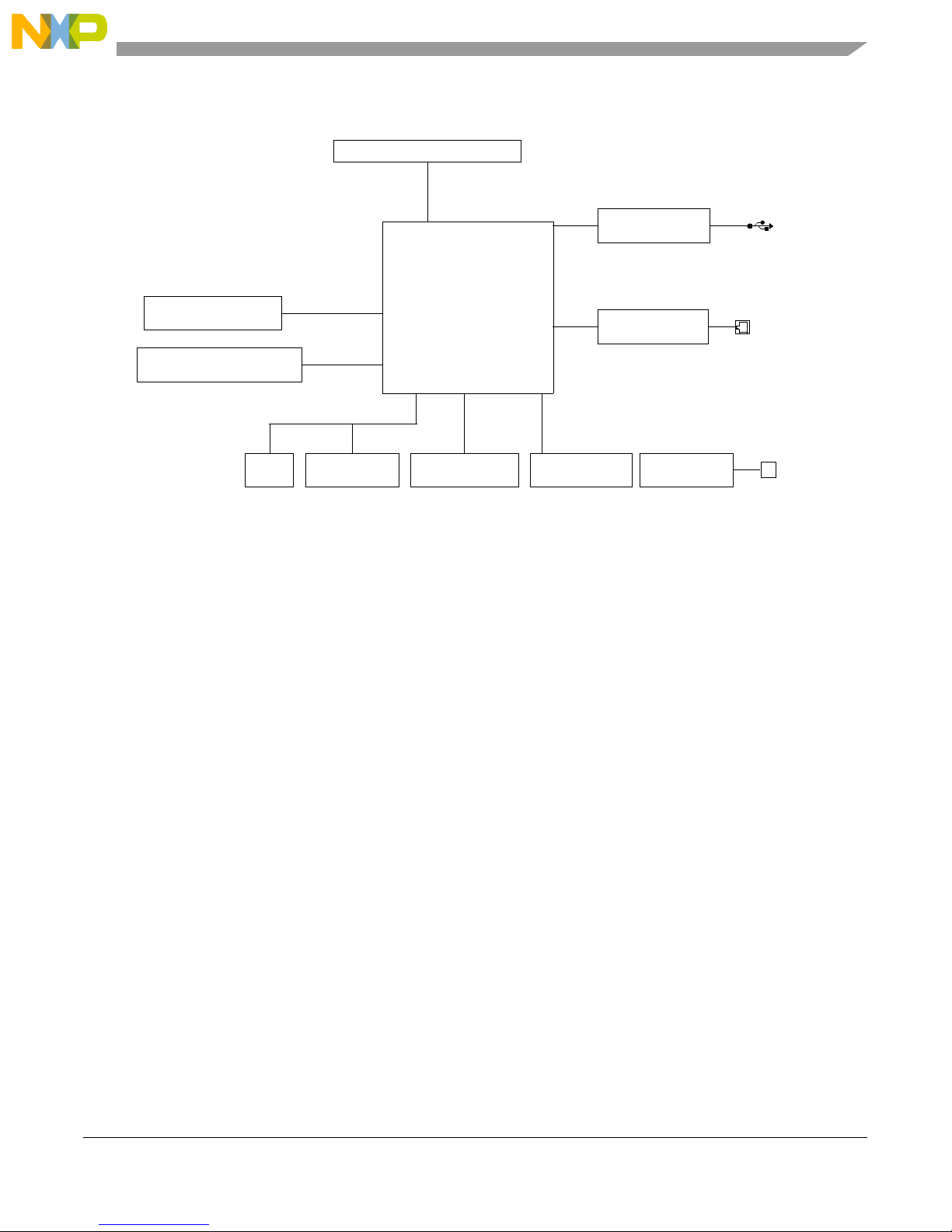
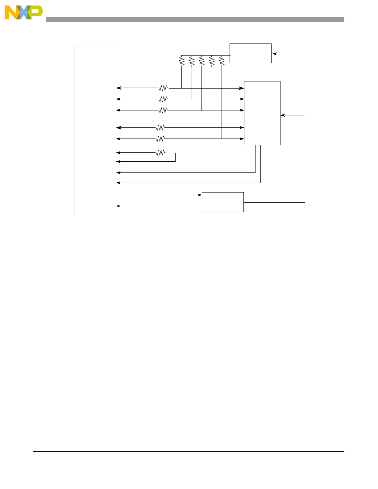
Figure 1 shows the MPC8349E-mITX-GP board block diagram.
32-Bit PCI Slot
33/66 MHz
PCI
ULPI1
MPC8349E-mITX-GP Board
USB PHY
8 Mbyte Flash
64 Mbyte ~ 1 Gbyte DDR
RTC EEPROM
Local Bus
DDR Bus
I2C
MPC8349E
RS-232 x 2
GMII
JTAG/COP
GbE PHY
Power
1 x GbE
Power
Figure 1. MPC8349E-mITX-GP Board Block Diagram
1.2 Board-Level Functions
The board-level functions discussed in this section are reset, interrupts, and clock distribution.
1.2.1 Reset and Reset Configurations
The MPC8349E-mITX-GP reset module generates a single reset to reset the MPC8349E and other
peripherals on the board. The reset unit provides power-on reset, hard reset, and soft reset signals in
compliance with the MPC8349E hardware specification.
MPC8349E-mITX-GP Reference Design Platform User’s Guide, Rev. 0
Freescale Semiconductor 3
Preliminary—Subject to Change Without Notice
Page 4
MPC8349E-mITX-GP Board
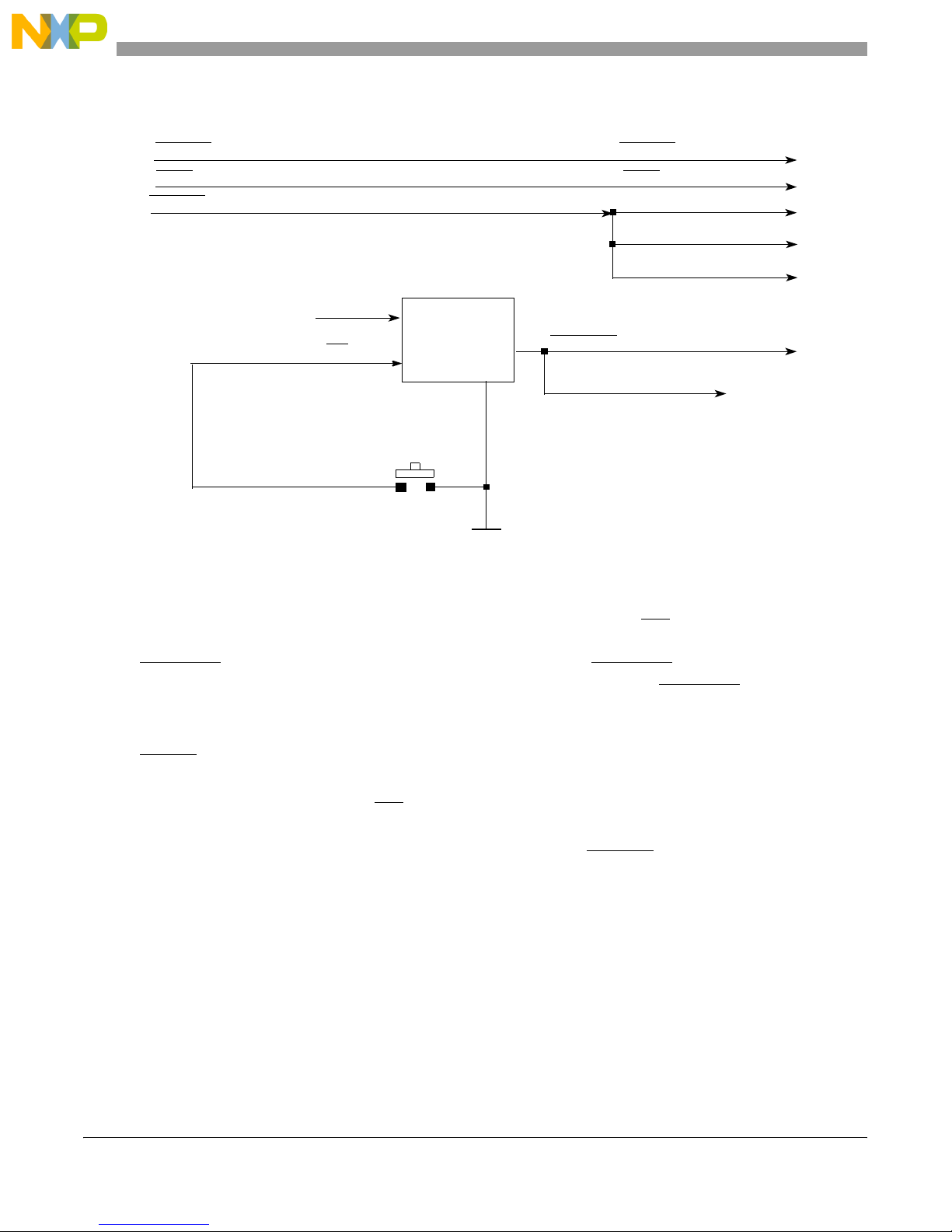
Figure 2 shows the reset circuitry.
SRESET
TRST
HRESET from COP
from COP
from COP
3.3 V
MAX811
MR
Push Button
GND
Figure 2. Reset Circuitry of the MPC8349E
PORESET
FLASH
to MPC8349E
SRESET
TRST
to MPC8349E
to MPC8349E
MPC8349E
10/100/1000 PHY
USB PHYs
• Hard reset is generated either by the COP/JTAG port or the MPC8349E.
• Power-on reset is generated by the Maxim MAX811 device. When MR is deasserted and 3.3 V is
ready , the MAX81 1 internal timeout guarantees a minimum reset active time of 150 ms before
PORESET is deasserted. This circuitry guarantees a 150 ms PORESET pulse width after 3.3 V
reaches the right voltage level, and this meets the specification of the PORESET input of
MPC834x.
• COP/JTAG port reset provides convenient hard-reset capability for a COP/JT AG controller. The
RESET line is available at the COP/JTAG port connector. The COP/JTAG controller can directly
generate the hard-reset signal by asserting this line low.
• Push button reset interfaces the MR
signal with a debounce capability to produce a manual master
reset of the processor card.
• Soft reset is generated by the COP/JT AG port. Assertion of SRESET causes the MPC8349E to
abort all current internal and external transactions and set most registers to their default values.
MPC8349E-mITX-GP Reference Design Platform User’s Guide, Rev. 0
4 Freescale Semiconductor
Preliminary—Subject to Change Without Notice
Page 5
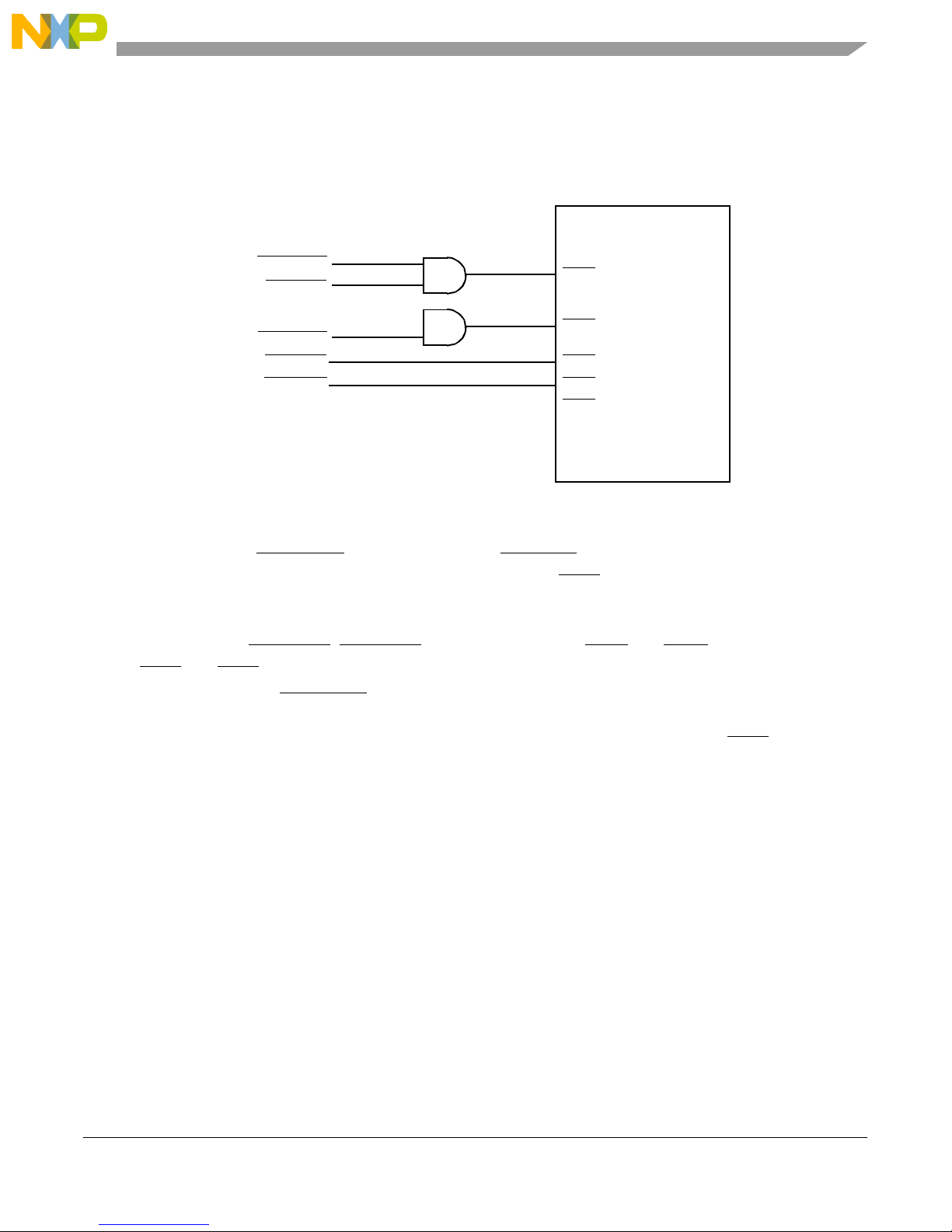
1.2.2 External Interrupts
Figure 3 shows the external interrupt circuitry to the MPC8349E.
External Logic
MPC8349E-mITX-GP Board
GBE1_IRQ
RTC_IRQ
USB2_IRQ
PCI_INTA
PCI_INTB
Figure 3. MPC8349E Interrupt Circuitry
IRQ2
IRQ3
IRQ4
IRQ5
IRQ6
MPC8349E
Following are descriptions of the interrupt signals shown in Figure 3:
• PHY interrupt (GBE1_IRQ) and RT C interrupt (RTC_IRQ).The VSC8201 GBE PHY interrupt is
ORed with the DS1339 RTC interrupt and connected to IRQ2 of the MPC8349E. Therefore, the
system software can detect the status of the Ethernet link, the PHY internal status, and the R TC
status.
• PCI interrupt (PCI_INTA, PCI_INTB). The 32-bit PCI slot I N TA and INTB are connected to the
IRQ4 and IRQ5 of the MPC8349E, respectively.
• USB over current (USB2_IRQ) . The USB2 power s upply has an over current detection circuit and
generate an interrupt when the current limit reaches (2A) or a thermal shutdown or under voltage
lockout (UVLO) condition occurs. This interrupt pin generates an interrupt to IRQ3 of the
MPC8349E.
MPC8349E-mITX-GP Reference Design Platform User’s Guide, Rev. 0
Freescale Semiconductor 5
Preliminary—Subject to Change Without Notice
Page 6
MPC8349E-mITX-GP Board
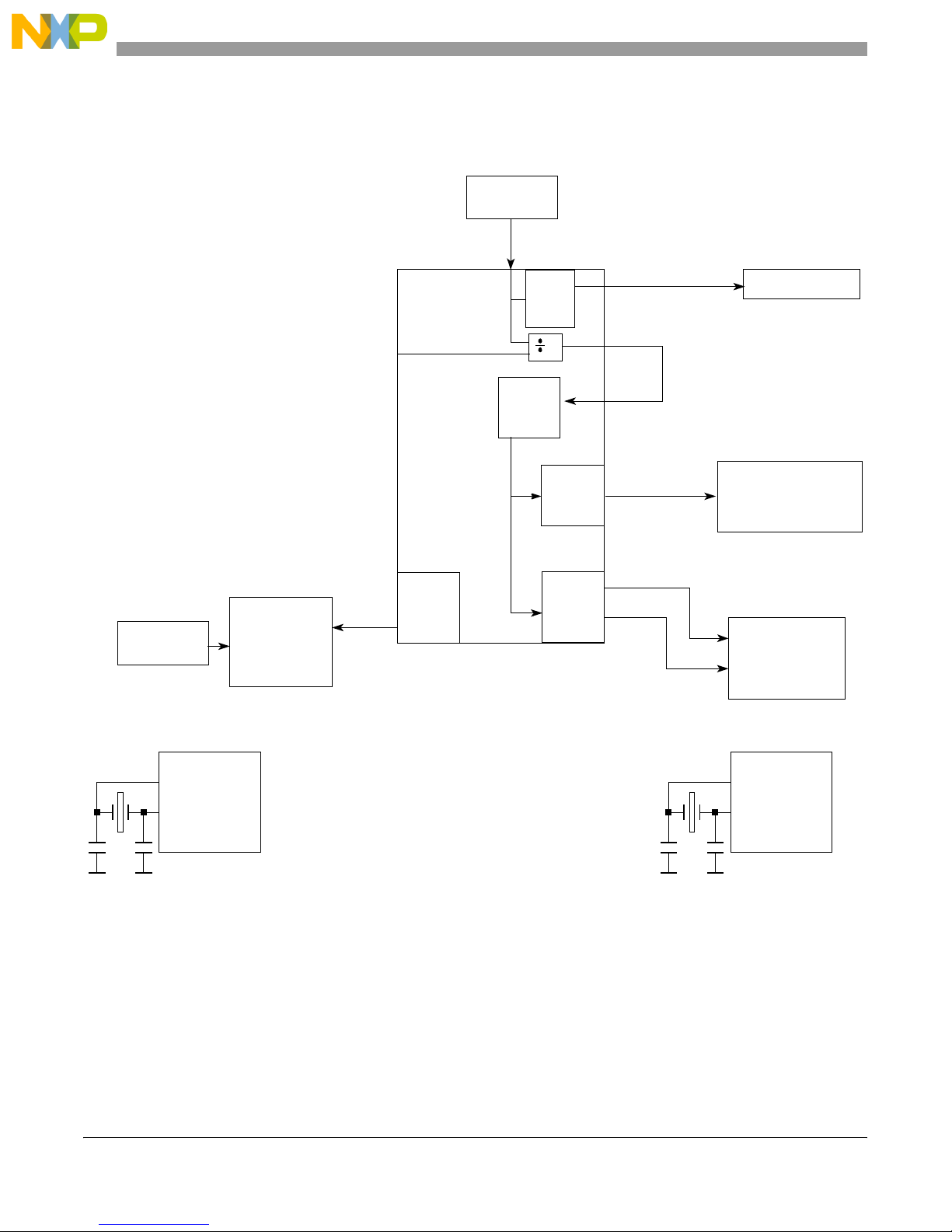
1.2.3 Clock Distribution
Figure 4 and Table 1 show the clock distribution on the MPC8349E-mITX-GP board.
66.666 MHz
OSC
CLKIN
33/66 MHz
PCI_SYNC_OUT
GPL5
CFG_CLKIN_DIV
PCI
DIV
OCCR
2
32-bit PCI Slot
25 MHz
24 MHz
Crystal
OSC
USB3300
VSC8201
125 MHz
TSEC
System
PLL
MPC8349E
local bus
DLL
DDR
DLL
PCI_SYNC_IN
LCLKx
33 MHz to 133 MHz
Local Bus CLK
MCKx
MCKx
133 MHz
DDR SDRAM
CLK
32.768 KHz
Crystal
DS1339
GND GND
Figure 4. MPC8349E-mITX-GP Clock Scheme
MPC8349E-mITX-GP Reference Design Platform User’s Guide, Rev. 0
6 Freescale Semiconductor
GND GND
Preliminary—Subject to Change Without Notice
Page 7

MPC8349E-mITX-GP Board
Table 1. Clock Distribution
Clock Frequency Module Generated by Description
66.666 MHz MPC8349E CLKIN 66.666 MHz oscillator The MPC834x uses CLKIN to generate the
PCI_SYNC_OUT clock signal, which is fed back
on the board through the PCI_SYNC_IN signal
to the internal system PLL. From the power-on
reset configuration, the CSB clock is generated
by the internal PLL and is fed to the e300 core
PLL for generating the e300 core clock. The
GPL5 (CFG_CLKIN_DIV) configuration input
selects whether CLKIN or CLKIN/2 is driven on
the PCI_SYNC_OUT signal. The GPL5 is tied to
jumper J22.D.
125 MHz MPC8349E TSEC VSC8201 For TSEC operation, a 125 MHz clock is
provided by the gigabit Ethernet PHY
(VSC8201) on the board.
133/166 MHz DDR SDRAM MPC8349E The DDR memory controller is configured to use
the 1:1 mode CSB to DDR clock for the DDR
interface. The local bus clock uses CCB/n clock,
where n is configured from the LCRR register.
25 MHz GBE PHY (VSC8201) 125 MHz oscillator The 25 MHz oscillator generates the clock for
the VSC8201
33/66 MHz PCI 32-bit slot MPC8349E The PCI module uses the PCI_SYNC_IN as its
clock source. The trace of the PCI_SYNC_IN/
PCI_SYNC_OUT signal is synchronized with all
the PCI signals of the PCI slots. The trace length
of the PCI_SYNC_IN/PCI_SYNC_OUT clock is
2.5 inches from the pin of the PowerQUICC II
Pro device to the PCI sockets.
24 MHz USB PHY2 (USB3300) 24 MHz crystal
32.768 KHz RTC (DS1339) 32.768 KHz crystal
1.2.4 DDR SDRAM Controller
MPC8349E uses DDR SDRAM as the system memory. The DDR interface uses the SSTL2 driver/receiver
and 2.5 V power. A Vr ef 2.5V/2 is needed for all SSTL2 receivers in the DDR interface. For details on
DDR timing design and termination, refer to the Fr eescale application note entitled Hardw ar e and Layout
Design Considerations for DDR Memory Interfaces (AN2582). The termination scheme uses one series
resistor (R
termination rail (V
The MPC8349E reads the DIMM SPD data using the DIMM SCL (clock) and the SDA (data) signals
through the I2C2 interface. Figure 5 shows the DDR SDRAM controller connection.
) from the MPC8349E to the memory and one termination resistor (RT) attached to the
S
). This approach is used in commodity PC motherboard designs.
TT
MPC8349E-mITX-GP Reference Design Platform User’s Guide, Rev. 0
Freescale Semiconductor 7
Preliminary—Subject to Change Without Notice
Page 8
MPC8349E-mITX-GP Board
MPC8349E
DDR
SDRAM
Controller
DQ[0:63]
DQM[0:7]
DQS[0:7]
A[0:13], BA[0,1],CTRL
MCK[0:3] pairs
MSYNC_OUT
MSYNC_IN
I2C– SCK2
I2C–SDA2
V
1.25 V
ref
Figure 5. DDR SDRAM Connection
2.5 V Input
VTT 1.25 V
V
Generator
ref
VTT
Generator
SDRAM
DIMM184
DDR
2.5 V Input
V
ref
1.2.5 Local Bus Controller
The MPC8349E local bus controller has a 32-bit LAD[0–31] address that consists of data multiplex bus
and control signals. The local bus speed is up to 133 MHz. T o interface with the standard memory device,
an address latch must provide the address signals. The LALE is used as the latchi ng signal. To reduce the
load of the high speed 32-bit local bus interface, there is a data buffer for all low-speed devices attached
to the memory controller. The on-board single bank 8-Mbyte Flash memory module is connected to the
local bus.
MPC8349E-mITX-GP Reference Design Platform User’s Guide, Rev. 0
8 Freescale Semiconductor
Preliminary—Subject to Change Without Notice
Page 9
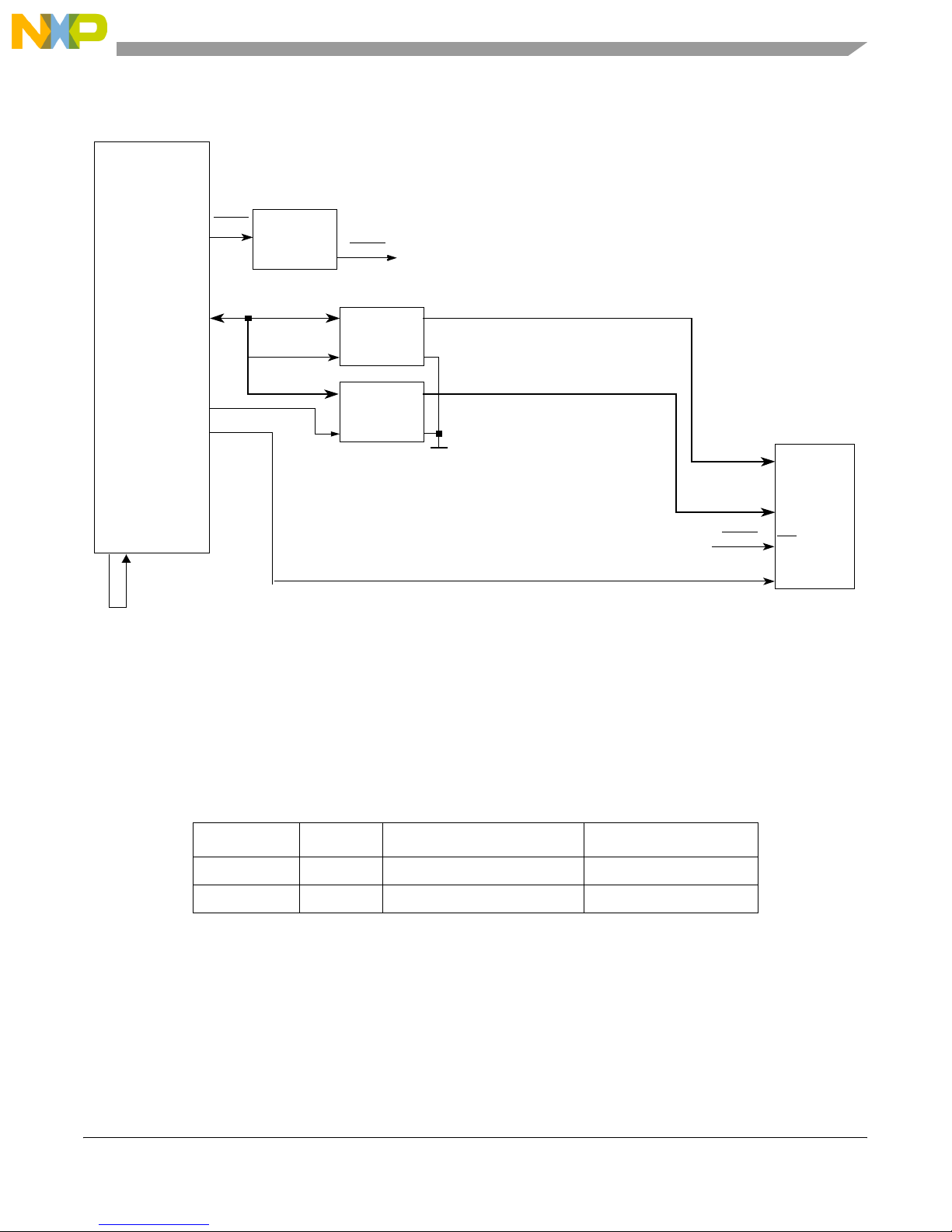
Figure 6 shows the block diagram and connections for the local bus.
MPC834E
Local Bus
Controller
LCS0
LCS0
Boot Flash
Select
Jumpers
F1CS
MPC8349E-mITX-GP Board
LAD[0:31]
BADDR[27:29]
ALE
LBCTL
Control Signals
LSYNC_OUT
LSYN_IN
LCLK0
LCKE
LCLK1
LAD[8:31]
LAD[0:15]
Address
Latch
LE
Buffer
DIR
Data
OE
OE
GND
A[9:30]
D[0:15]
F1CS
Control
Flash Memory
A[21:0]
D[15:0]
CS
Control
MX29LV640M
Figure 6. Local Bus Connections
1.2.6 On-Board Flash Memory
Through the general-purpose chip-select machine (GPCM), the MPC8349E-mITX-GP provides a total of
8 Mbyte of 90 ns Flash memory using one chip-select signal. The Flash memory is used with the 16-bit
port size.
J22.E BOOT1 Boot Flash Backup Flash
Jumper Off 1 Reserved Reserved
Jumper On 0 U7 U4
The starting address for the Flash bank is 0xFE00_0000 to 0xFE7F_FFFF.
1.2.7 I2C
The MPC8349E has two I2C interfaces. On the MPC8349E-mITX-GP board, the MPC8349E acts as I2C
master for both I
Freescale Semiconductor 9
2
C buses (I2C1 and I2C2). I2C1 is connected to the M24256 serial EEPROM, and I2C2
MPC8349E-mITX-GP Reference Design Platform User’s Guide, Rev. 0
Table 2. Boot Flash Selection
Preliminary—Subject to Change Without Notice
Page 10

MPC8349E-mITX-GP Board
is connected to the DDR DIMM module SPD (serial presence detect) EEPROM, the two PCF8574 I2C
expanders, the DS1339 RTC (real time clock).
The M24256 serial EEPROM can be used to s tore the reset configuration word of the MPC8349E, as well
as storing the configuration registers values if boot sequencer of MPC8349E is enabled. If user wants to
load the reset configuration word from the I2C1 M24256 EEPROM, the jumper J22 should be set to
ABCDEFGH=01011110, with 1=jumper removed and 0=jumper installed. For more details on how to
program the reset configuration word value in I2C EEPROM and the boot sequencer mode, please refer to
the MPC8349ERM. The I2C address of the M24256 EEPROM on I 2C1 bus is 0x50.
The DDR SPD EEPROM is connected to the I2C2 of MPC 8349E. The bootload program optionally reads
the SPD EEPROM data to determine the DDR DIMM physical structure (e.g. number of rows and
columns), the DDR timings (e.g. CAS latency, re-fresh timing), and setup the configuration registers of
the MPC8349E DDR memory controller . The I2C address of the DDR SPD EEPROM on I2C2 bus is 0x51.
There are two PCF8574A I2C I/O expander on the MPC8349E-mITX-GP board to provide general
purpose I/O expansion via the I2C2 interface. The first PCF8574A (U8) has I2C2 address 0x38 and it is
able to control the Green LED (D1) and Yellow LED (D2), set the VSC8201 to powerdown mode. The bit
definition of this PCF8574A (U8) is defined as in Table 3.
Table 3. PCF8574A (U8) Bit Descriptions
PCF8574A (U8)
Bit[0..7]
0LED0Write only,
1 LED1 Write only,
2 VSC8201_PWN Write only,
3
4 LCD_EN Write only,
5 Not used — —
6 Not used — —
7 Not used — —
Name Read/Write Description
LED0 control
Reserved
read returns 1
read returns 1
read returns 1
Write only,
read returns 1 Reserved
read returns 1 Reserved
0: LED is on
1: LED is off
LED1 control
0: LED is on
1: LED is off
VSC8201 power down control
0: VSC8201 PHY is powerdown
1: VSC8201 PHY in normal mode
The second PCF8574A (U10) has I2C2 address 0x39 and it is able to detect the board revision number,
the PCI M66EN signal level and detect which Flash is currently used to boot. The bit definition of this
PCF8574A (U10) is defined as in Table 4.
MPC8349E-mITX-GP Reference Design Platform User’s Guide, Rev. 0
10 Freescale Semiconductor
Preliminary—Subject to Change Without Notice
Page 11

Table 4. PCF8574A (U10) Bit Descriptions
MPC8349E-mITX-GP Board
PCF8574A
(U10) bit[0..7]
0 REV1 Read only, write
1 REV0
2 Reserved Read only, write
3
4 MPCI_CLKRUN Read/Write
5 PCI_M66EN Read only, write
6 BOOT0 Read only, write
Name Read/Write Description
Read only, write
Reserved
Board revision number
has no effect
has no effect
has no effect Reserved
has no effect
has no effect
REV[0:1] definition
00: revision 0.0
01: revision 0.1
10: revision 1.0
11: reserved
Reserved for future use
Reserved
PCI M66EN Signal
0: PCI M66EN signal is low, indicates the PCI cards on PCI slot is
not 66 MHz capable
1: PCI M66EN signal is high, indicates the PCI cards on PCI slot is
66 MHz capable
Used to determine which Flash is used for boot Flash
0: Reserved
1: Flash 1 (U7) is the boot Flash
7 Not used — —
The DS1339 R TC is connected to I2C with address 0x68. The software running on PowerPC core can read
or write to the RTC through the I2C2 interface.
1.2.8 10/100/1000 BaseT Interface
On the MPC8349E-mITX-GP board, GMII mode is used on TSEC1 , which is connected to the on-board
10/100/1000 PHY (VSC8201). The TSEC I/O voltage is s et to 3. 3 V. The GMII (1000 BaseT) is a source
synchronous bus. For a transmit bus connection, it is synchronous to GTX_CLK from the TSEC module.
The receive bus connection is synchronous to RX_CLK generated from the PHY device. When the speed
is 10/100 BaseT (MII), both t ransmit and re ceive clocks ar e generated by the VSC8201 PHY device. The
MPC8349E MII management interface is connected to the VSC8201 only . Figure 7 shows the connection
between the MPC8349E TSEC1 to the VSC8201.
MPC8349E-mITX-GP Reference Design Platform User’s Guide, Rev. 0
Freescale Semiconductor 11
Preliminary—Subject to Change Without Notice
Page 12

MPC8349E-mITX-GP Board
MPC8349E
TSEC1
TX_ER
TX_EN
GTX_CLK
TXD[0:7]
TX_CLK
COL
RX_ER
RX_DV
RX_CLK
RXD[0:7]
EC_MDIO
EC_MDC
LVDDx
GMII interface
3.3 V
Figure 7. GMII Interface Connection for 10/100/1000 BaseT Ethernet
1.2.9 RS-232 Port
PHY addr = 0x1C
VSC8201
TXER
TXEN
GTX_CLK
TXD[0:7]
TXC
COL
CRSCRS
RXER
RXDV
RX_CLK
RXD[0:7]
MDIO
MDC
RJ-45
(Enet0)
Figure 8 illustrates the serial port connection using a MAX3232 3.3 V RS-232 driver to interface with a
9-pin D type female connector. This serial connection runs at up to 115.2 Kbps.
MAX3232
MPC8349E
UART0
CTS
TXD
RTS
DO
DO
DI
DI
RXRXD
RX
TX
TX
RXD
CTS
TXD
RTS
DB-9
RS-232
Serial
Por t
Figure 8. UART Debug Port Connection
1.2.10 USB 2.0 Interface
The MPC8349E has two internal USB modules (USB0 and USB1), a multi-port host (MPH) module, and
a dual-role (DR) module. On the MPC8349E-mITX-GP board, USB1 connects to USB PHY (USB3300)
through the 8-bit UTMI low pin count interface (ULPI). The USB3300 PHY connects to a USB Mini-AB
type receptacle connector that serves as a host/device/ OT G USB inter fac e. Table 5 shows the USB0 and
USB1 configuration. Note that OTG software support is subject to Linux kernel support.
MPC8349E-mITX-GP Reference Design Platform User’s Guide, Rev. 0
12 Freescale Semiconductor
Preliminary—Subject to Change Without Notice
Page 13

MPC8349E-mITX-GP Board
Table 5. USB Port 0 and Port 1 Configurations
Port Interface Type USB PHY Operating Mode Connector Type
USB Port 1 ULPI USB3300 DR Host/Device/OTG 1 x Type Mini-AB Receptacle
Figure 9 shows the connection of USB port 0 and port 1.
MPC8349E
USB3300
ULPI_D[7:0]
ULPI_DIR
ULPI_STP
ULPI_NXT
Por t 1
ULPI_CLK
CPEN
D[7:0]
DIR
STP
NXT
CLKOUT
Figure 9. USB Port 0 and Port 1 Connections
VBUS
DM
DP
ID
MIC2505
5 V
USB Type Mini-AB
1.2.11 PCI Subsystem
The MPC8349E has two PCI interfaces (PCI1 and PCI2). PCI1 interface is not used. PCI2 connects to a
32-bit 3.3 V PCI slot.
MPC8349E
PCI2-AD[0:31]
PCI2-CBE
32-Bit PCI2
[0:3]
PCI2-CTRL
PCI2-GNT0
PCI2-REQ0
PCI2-GNT0
PCI2-REQ0
32-Bit 3.3 V
PCI Slot
Figure 10. PCI Subsystem
1.2.12 COP/JTAG Port
The common on-chip processor (COP) is part of the MPC8349E JTAG module and is implemented as a
set of additional ins tructions and logi c. This por t can connect to a dedicated emulator for extensive system
debugging. Several third-party emulators in the market can connect to the host computer through the
MPC8349E-mITX-GP Reference Design Platform User’s Guide, Rev. 0
Freescale Semiconductor 13
Preliminary—Subject to Change Without Notice
Page 14

MPC8349E-mITX-GP Board
Ethernet port, USB port, parallel port, RS-232, and so on. A typical setup using a USB port emulator is
shown in Figure 11.
PC
P17
USB
Emulator
MPC8349E ITX
Figure 11. Connecting the MPC8349E-mITX-GP Board to A Parallel Emulator
The 16-pin generic header connector carries the COP/JTAG signals and the additional signals for system
debugging. The pinout of this connector is shown in Figure 12.
1
TDO
TDI
Pull-up
TCK
TMS
SRESET
HRESET
CKSTP_OUT
GND
TRST
Pull-up
NC
GND
GND
NC
GND
Figure 12. MPC8349E-mITX-GP Board COP Connector
MPC8349E-mITX-GP Reference Design Platform User’s Guide, Rev. 0
14 Freescale Semiconductor
Preliminary—Subject to Change Without Notice
Page 15

MPC8349E-mITX-GP Board
1.3 MPC8349E-mITX-GP Assembly
The MPC8349E-mITX-GP board PCB top view is shown in Figure 13, with the references of LEDs,
jumpers, headers, and switches.
P1
32-bits PCI
P14
ENET0 (top)
Reserved (bottom)
J19
S3
J21
BT1 Battery Holder
P17
COP Connector
U1 DIMM184 DDR1
ABCDEFGH
P18 ATX Power
J22
J14
J9
D1
D9 D2
J10
D8
S5 PowerOn
P11
USB5
P15 RS-232-COM1
Pin 1
Figure 13. MPC8349E-mITX-GP Top View
1.4 Connectors
This section describes the MPC8349E-mITX-GP connectors and their pin assignments.
1.4.1 Case Connector
The case connector (J10) connects to the case power switch, power LED, reset switch.
• PWR_SW can connect to the 2-pin power push button on the front panel.
• PWR_LED lights when the system is turned ON.
• RST_SW can connect to the 2-pin reset push button on the front panel.
MPC8349E-mITX-GP Reference Design Platform User’s Guide, Rev. 0
Freescale Semiconductor 15
Preliminary—Subject to Change Without Notice
Page 16

MPC8349E-mITX-GP Board
Table 6 lists the pin assignments of the case connector.
Table 6. Case Connector J10 Pin Assignments
Pin Signal
1 Power LED K
2 Power LED A
3 Power LED A
4GND
5 Power On
6GND
7 RESET
8–15 Reserved
1.4.2 COP Connector
The COP connector (P17) allows the user to connect a COP/JTAG-based debugger to the
MPC8349E-mITX-GP board for debugging. Table 7 lists the pin assignments of the COP connector.
Table 7. COP Connector Pin Assignments
Pin Signal Pin Signal
1 TDO 2 GND
3 TDI 4 TRST
5QREQ 6 VDD_SENSE
7 TCK 8 CHKSTOP_IN
9TMS 10 NC
11 SRESET
13 HRESET
12 NC
14 GND
1.4.3 PCI Slot
The MPC8349E-mITX-GP board has one 32-bit 3.3 V PCI expansion slot (P1) for an expansion card.
WARNING
Only the 3.3 V PCI Card is supported. Turn OFF power during insertion and
removal of PCI card.
MPC8349E-mITX-GP Reference Design Platform User’s Guide, Rev. 0
16 Freescale Semiconductor
Preliminary—Subject to Change Without Notice
Page 17

MPC8349E-mITX-GP Board
3.3 V PCI cards can be identified by the key position on the PCI car d, as shown in Figure 14.
PCI Slot
5 V Key
DIMM
Match
3.3 V Key
Here
RJ-45
Figure 14. 3.3 V Key on a Typical 3.3 V PCI Card
1.4.4 Fan Connectors
There are two fan connectors on the MPC8349E-mITX-GP board, one for powering a 5 V fan (J9) and the
other for powering a 12 V fan (J5). For typical fans, the red wire is always positive (+) and the black wire
is always negative (–).
1.4.5 Battery Holder
The MPC8349E-mITX-GP board contains an RTC that requires a battery to maintain the data inside the
RTC. The battery holder (BT1) accommodates a CR-2032. Figure 15 shows how to insert a battery.
Battery Holder
1.4.6 Power Connector
P18 is compatible with connectors from A T X power supply, supplying necessary DC power to the
MPC8349E-mITX-GP board.
MPC8349E-mITX-GP Reference Design Platform User’s Guide, Rev. 0
Freescale Semiconductor 17
CR-2032 Lithium Battery
2. Press
1. Insert
Figure 15. Installation of Battery
Preliminary—Subject to Change Without Notice
Page 18

MPC8349E-mITX-GP Board
1.5 Jumpers, Switches, and LED Indicators
This section shows the default settings and descriptions of jumpers, switches, and LED indicators.
1.5.1 Powerup Configuration Jumpers
The powerup configuration jumpers at J22 sets up the system configurations. Figure 16 shows the factory
default configuration of J22.
Jumper On
AB CDEFGH
Figure 16. Powerup Configuration Jumpers (J22)
Table 8 describes the position of each jumper.
Table 8. Description of Jumper J22 Positions
Default
Posit ion Name
A LGPL0 ON (0) 000 local bus EEPROM (Default)
BLGPL1 ON (0)
CLGPL3 ON (0)
D LGPL5 OFF (1) OFF (1): Default
ON = Jumper Is On
OFF = Jumper Is Off
2
C EEPROM,PCI_CLK/PCI_SYNC_IN 25–44 MHz
001 I
2
C EEPROM,PCI_CLK/PCI_SYNC_IN 25–66.666 MHz
010 I
011 Hard-coded option, 66 MHz, 266 MHz, 400 MHz (PCI, CSB, CPU)
100 Hard-coded option, 33 MHz, 266 MHz, 400 MHz
101 Hard-coded option, 33 MHz, 133 MHz, 266 MHz
110 Hard-coded option, 33 MHz, 166 MHz, 333 MHz
111 Hard-coded option, 66 MHz, 266 MHz, 533 MHz
Hard-coded option is used in conjunction with JTAG debug
CLKIN: PCI_SYNC_OUT = 2:1 PCI_CLK_OUT[0:7] = OCCR (max CLKIN/2).
66 MHz CLKIN is used and 33 MHz PCI2.
ON (0):
CLKIN: PCI_SYNC_OUT = 1:1, PCI_CLK_OUT[0:7] = CLKIN. 66 MHz
CLKIN is used, 66 MHz PCI2.
Jumper Off
Description
EBOOT1
18 Freescale Semiconductor
OFF(1) OFF (1): Default
MPC8349E-mITX-GP Reference Design Platform User’s Guide, Rev. 0
MPC8349E fetches the reset vector from Flash 0 (U4).
ON (0): Reserved
Preliminary—Subject to Change Without Notice
Page 19

Table 8. Description of Jumper J22 Positions
Default
Posit ion Name
F PCI_M66EN ON (0) OFF (1):
ON = Jumper Is On
OFF = Jumper Is Off
MPC8349E-mITX-GP Board
Description
M66EN signal is determined by the card plugged into the PCI slot (PCI 32-bit
slot and MiniPCI slot).
ON (0): Default
M66EN signal is hardwired to 0, which is hard coded to 33 MHz PCI
operation.
G I2C-WP ON (0) OFF (1):
2
I
C EEPROM (U64) is write protected.
ON (0): Default
2
C EEPROM (U64) is not write protected.
I
HF_WP
OFF (1) OFF (1): Default
Flash (U7) are not write protected.
ON (0):
Flash (U7) are write protected.
Table 9 lists the connectors, jumpers, switches, and LEDs on the MPC8349E-mITX-GP board.
Table 9. Lists of Connectors, Jumpers, Switches, and LEDs
Reference Description
Connectors
BT1 Battery holder for RTC
J4 Background Debug Mode (BDM). Header for Flash programming and debug of on-board MC9S08QG8
Microcontroller.
J5 12V fan connector
J9 5 V fan connector
J10 Case connector
P1 32-bit 3.3 V PCI connector
P11 USB MiniAB connector
P14 RJ-45 connectors Enet0 (top). Typically Enet0 is the WAN connector. See Figure 7.
P15 COM1 serial port terminal connector (RS-232)
P17 14 pins COP/JTAG connector
P18 ATX Power connector
U1 DIMM184 DDR1 connector
J14 CPU power control jumper. Selects ATX power supply on/off to be controlled by push button S5 (jumper 2–3
as default) or MCU firmware (jumper 1–2).
MPC8349E-mITX-GP Reference Design Platform User’s Guide, Rev. 0
Freescale Semiconductor 19
Jumpers
Preliminary—Subject to Change Without Notice
Page 20

MPC8349E-mITX-GP Board
Table 9. Lists of Connectors, Jumpers, Switches, and LEDs (continued)
Reference Description
J19 CPU Power-on reset source jumper. CPU Power-On Reset can be controlled by a hardware MAX811 reset
chip (jumper 2–3 as default).
J21 Real time clock selector. CPU real time clock interrupt request can be selected from DS1339 real time clock,
[ jumper 2–3]. Default is not selected.
J22 Reset configuration word source selection jumpers
Switches
S3 System reset button. Resets the MPC8349E-mITX-GP board.
S5 Power-on push button. Powers up the MPC8349E-mITX-GP board.
LEDs
D1/D2 SW0 and SW1. Controlled by the I2C expander connected to the MPC8349E
D8 USB port power indicator LED. Lights when power is enabled on USB (D8).
D9 3.3 V Active. On means 3.3 V power is good.
1.6 MPC8349E-mITX-GP Board Configuration
This section describes the operational mode and configuration options of the MPC8349-mITX-GP board.
1.6.1 Flash Memory
The Flash memory bank is MX29LV640MTTC-90 top boot Flash memory devices. Each Flash memory
bank has 135 sectors. The first 127 sectors, SA[0–126], are 64 Kbyte, and the last 8 sectors, SA[127–134],
are 8 Kbyte. These last 8 sectors can be write-protected to prevent accidental erasure of the sector content
for applications that may choose to use this protection feature. Table 10 shows the jumper settings to
write-protect sectors SA[127–134] of Flash memory.
Table 10. Flash Memory Write Protect of SA[127–134]
J22.H Description
Jumper Off Flash (U7) top sectors are not write protected (WP
Jumper On Flash (U7) top sectors are write protected (WP
not asserted).
asserted).
1.6.2 EEPROM
An on-board serial EEPROM allows storage of miscellaneous board-related data. The EEPROM can be
write-protected by S2.SW3, as shown in Table 11.
MPC8349E-mITX-GP Reference Design Platform User’s Guide, Rev. 0
20 Freescale Semiconductor
Preliminary—Subject to Change Without Notice
Page 21

Table 11. EEPROM Write Protect
J22.G Description
MPC8349E-mITX-GP Board
Jumper Off Serial EEPROM is write protected (WC
Jumper On Serial EEPROM is not write protected (WC
not asserted).
asserted).
1.6.3 PCI Operating Frequency
An M66EN input pin determines the AC timing of the PCI interface. On the MPC8349E-mITX-GP board,
the state of this signal can be driven to 0 by the J22 jumper to select 33 MHz AC timing. If J22.F is not
driven to 0, the M66EN signal level is determined by the PCI agent card connected to PC I slot P1. I f a 33
MHz only card is inserted, the M66EN signal is driven to 0 by the PCI agent card according to the PCI
specification, or it is driven to 1 if it can perform at 66 MHz. See Table 12.
.
Table 12. M66EN Signal Status Selection
J22.F Description
Jumper Off M66EN signal is determined by the card plugged into the PCI slot.
Jumper On M66EN signal is hardwired to 0, which is hard coded to 33 MHz PCI operation.
1.6.4 Reset Configuration Word
The reset configuration word (RCW) controls the clock ratios and other basic device functions such as PCI
host or agent mode, boot location, TSEC modes, and endian mode. The reset configuration word is divided
into reset configuration word lower (RCWL) and reset configuration word higher (RCWH) and is loaded
from the local bus during the power-on or hard reset flow. The default RCW low bit setting is
0x0404_0000. The default RCW high bit se tting is 0xB460_A000.
The RCW is located at the lowest 64 bytes of the boot Flash memory, which is 0xFE00_0000 if the default
memory map is used.
Table 13. Default RCW in Flash Memory
Address
FE000000: 04040404 04040404 04040404 04040404
FE000010: 00000000 00000000 00000000 00000000
FE000020: B0B0B0B0 B0B0B0B0 60606060 60606060
FE000030: A0A0A0A0 A0A0A0A0 00000000 00000000
MPC8349E-mITX-GP Reference Design Platform User’s Guide, Rev. 0
Freescale Semiconductor 21
Preliminary—Subject to Change Without Notice
Page 22

MPC8349E-mITX-GP Board
The RCW definitions are shown in Figure 17 and Figure 18.
0 1 2 3 4 5 6 7 8 9 10 11 12 13 14 15
Field LBIUCM DDRCM — SPMF — COREPLL
16 17 18 19 20 21 22 23 24 25 26 27 28 29 30 31
Field —
Figure 17. Reset Configuration Word Low (RCWL) Bit Settings
0 1 2 3 4 5 6 7 8 9 10 11 12 13 14 15
Field PCIHOST PCI64 PCI1ABR PCI2ABR COREDIS BMS BOOTSEQ SWEN ROMLOC —
16 17 18 19 20 21 22 23 24 25 26 27 28 29 30 31
Field TSEC1M TSEC2M — TLE LALE LDP —
Figure 18. Reset Configuration Word High (RCWH) Bit Settings
Table 14. RCWL Bit Descriptions
Bits Name Meaning Description
0 LBIUCM Local bus memory
controller clock
mode
1 DDRCM DDR SDRAM
memory controller
clock mode
2–3 — Reserved Must be cleared.
4–7 SPMF[0–3] System PLL
multiplication
factor
Local Bus Controller Clock: CSB_CLK
0: Default ratio 1:1
1: ratio 2:1
DDR Controller Clock: CSB_CLK
0: Default ratio 1:1
1: ratio 2:1
0000 16:1
0001 Reserved
0010 2:1
0011 3:1
0100 (default) 4:1
0101 5:1
MPC8349E-mITX-GP Reference Design Platform User’s Guide, Rev. 0
22 Freescale Semiconductor
Preliminary—Subject to Change Without Notice
Page 23

Table 14. RCWL Bit Descriptions (continued)
Bits Name Meaning Description
MPC8349E-mITX-GP Board
4–7 SPMF[0–3] System PLL
multiplication
factor
0110 6:1
0111 7:1
1000 8:1
1001 9:1
1010 10:1
1011 11:1
1100 12:1
1101 13:1
1110 14:1
1111 15:1
8 — Reserved Must be cleared.
9–15 COREPLL
[0–6]
Value coreclk: csb_clk VCO divider
nn 0000 n PLL bypassed PLL bypassed
00 0001 0 1:1 2
01 0001 0 1:1 4
10 0001 0 1:1 8
11 0001 0 1:1 8
00 0001 1 1.5:1 2
01 0001 1 1.5:1 4
10 0001 1 1.5:1 8
11 0001 1 1.5:1 8
00 0010 0: Default 2:1 2
9–15 COREPLL
[0–6]
01 0010 0 2:1 4
10 0010 0 2:1 8
11 0010 0 2:1 8
00 0010 1 2.5:1 2
01 0010 1 2.5:1 4
10 0010 1 2.5:1 8
11 0010 1 2.5:1 8
00 0011 0 3:1 2
01 0011 0 3:1 4
10 0011 0 3:1 8
11 0011 0 3:1 8
16–31 — Reserved. Must be cleared.
MPC8349E-mITX-GP Reference Design Platform User’s Guide, Rev. 0
Freescale Semiconductor 23
Preliminary—Subject to Change Without Notice
Page 24

MPC8349E-mITX-GP Board
Table 15. Reset Configuration Word High (RCWH) Bit Descriptions
Bits Name Meaning Detailed Description
0 PCIHOST PCI host mode 0 PCI agent
1: Default PCI host
1 PCI64 PCI 64 bit bus
mode
0: Default 32-bit PCI interface
1 64-bit PCI interface
2 PCI1ARB PCI1 arbiter 0 PCI1 arbiter disabled
1: Default PCI1 arbiter enabled
3 PCI2ARB PCI2 Arbiter 0 PCI2 arbiter disabled
1: Default PCI2 arbiter enabled
3 Reserved — Must be cleared
4 COREDIS Core disable mode 0: Default e300 enabled
1 e300 disabled
5 BMS Boot memory
space
6–7 BOOTSEQ Boot sequencer
configuration
0: Default 0x0000_0000–0x007F_FFFF
1 0xFF80_0000–0xFFFF_FFFF
00: Default Boot sequencer is disabled
01 Boot sequencer load configuration from I
10 Boot sequencer load configuration from EEPROM
11 Reserved
8 SWEN Software watchdog
enable
0: Default Disabled
1 Enabled
2
C
9–11 ROMLOC Boot ROM
interface location
000 DDR SDRAM
001 PCI1
010 PCI2
011, 100 Reserved
101 Local bus GPCM, 8 bits
110: Default Local bus GPCM, 16 bits
111 Local bus GPCM, 32 bits
12–15 Reserved — Must be cleared
16–17 TSEC1M TSEC1 Mode 00 RGMII
01 RTBI
10: Default GMII
10 TBI
MPC8349E-mITX-GP Reference Design Platform User’s Guide, Rev. 0
24 Freescale Semiconductor
Preliminary—Subject to Change Without Notice
Page 25

Table 15. Reset Configuration Word High (RCWH) Bit Descriptions (continued)
Bits Name Meaning Detailed Description
18–19 TSEC2M TSEC2 Mode 00 RGMII
01 RTBI
10: Default GMII
10 TBI
20–27 Reserved — Must be cleared
28 TLE True little endian 0: Default Big-endian mode
1 True little endian mode
MPC8349E-mITX-GP Board
29 LALE Local Bus ALE
signal timing
30 LDP LDP/CKSTP pin
mux state after
reset
31 Reserved — Must be cleared
0: Default Normal LALE timing
1 LALE is negated 1/2 lbiu_controller_clk earlier.
0: Default LDP[0] and
LDP[1] = local data parity.
1 LDP[0] = CKSTOP_OUT and LDP[1] =
CKSTOP_IN.
1.6.4.1 Reset Configuration Word SPMF[0–3] and COREPLL[0–6]
CLKIN is the input to the CCB PLL to generate the CCB clock, which pr ovides the platform logic.
Table 16 shows the common combinations of CLKIN, CCB, and the core frequency and their respective
ratios.
Table 16. Core PLL Ratio
CCB
CLKIN
66.666 MHz 0101 333 MHz 5:1 00 0010 0 667 MHz 2:1
SPMF
[0–3]
CCB
clock:
CLKIN
Ratio
COREPLL
[0–6]
Core
Frequency
CCB Clock:
CLKIN Ratio
66.666 MHz 0100 266 MHz 4:1 00 0010 1 667 MHz 2.5:1
66.666 MHz 0011 200 MHz 3:1 00 0010 0 600 MHz 3:1
66.666 MHz 0101 333 MHz 5:1 01 0001 1 500 MHz 1.5:1
66.666 MHz 0100 266 MHz 4:1 00 0010 0 533 MHz 2:1
66.666 MHz 0011 200 MHz 3:1 00 0010 1 500 MHz 2.5:1
66.666 MHz 0101 333 MHz 5:1 00 0001 0 333 MHz 1:1
66.666 MHz 0100 266 MHz 4:1 01 0001 1 400 MHz 1.5:1
66.666 MHz 0011 200 MHz 3:1 01 0010 0 400 MHz 2:1
MPC8349E-mITX-GP Reference Design Platform User’s Guide, Rev. 0
Freescale Semiconductor 25
Preliminary—Subject to Change Without Notice
Page 26

MPC8349E-mITX-GP Board
1.6.4.2 Example of Changing the RCW Register Using Uboot
Issue the following uboot commands to change from 533/266 to 400/266 (CPU/CCB):
cp.b FE000000 100000 40
mw.b 100008 23 8
md 100000
erase FE 000 00 0 FE00FFFF
md FE000000
cp.b 100000 FE000000 40
md FE000000
reset
To make the changes take effect, power off the system and then power it on. Figure 19 shows the change
in bit settings from these uboot commands. There is no change in the SPMF field since 0b0100 is the
default value representing the 266 MHz CCB frequency. The COREPLL field is changed from the default
value of 0b000_0100 representing 533 M Hz to the new value of 0b010_001 1 representing 400 MHz core
frequency.
034789 15
Field — SPMF — COREPLL
Bit Setting0100010000100011
Figure 19. Reset Configuration Word Low (RCW) Bit Settings Example
1.6.5 Power Supply
The MPC8349E requires a 3.3 V and 5 V power supply from the ATX power connector for normal
operation. The 3.3 V power supply is reduced to 1.2 V and 2.5 V. The 1.2 V power is generated from a
switching power supply for a CPU core. The 2.5 V power is generated from an LDO regulator for the DDR
controller.
MPC8349E-mITX-GP Reference Design Platform User’s Guide, Rev. 0
26 Freescale Semiconductor
Preliminary—Subject to Change Without Notice
Page 27

Figure 20 shows the power supply block diagram.
MPC8349E-mITX-GP Board
5 V
USB VBUS Power
1.2 V
MPC8349E Vcore
2.5 V
DDR
3.3 V
5 V input
3.3 V input
MIC2505
MAX1953
5 V
CPU Fan
MIC29302
Figure 20. Power Supply Circuitry
The core supply voltage and I/O supply voltages do not have to be applied in any particular order. During
the power ramp up, before the power supplies are stable, there may be an interval when the I/O pins are
actively driven. After power is stable, as long as PORES ET is asserted, most I/O pins are three-stated. To
minimize the time I/O pins are actively driven, apply core voltage before I/O voltage and assert PORESET
before the power supplies fully ramp up. In general, for a dual-supply voltage device, minimize the voltage
difference between the V
core
and V
during ramp-up and power-down.
I/O
1.6.6 Chip-Select Assignments and Memory Map
Table 17 shows an example memory map on the MPC8349E that is used for u-boot 1.1.3 in the Flash
memory.
Table 17. Example Memory Map, Local Access Window, and Chip-Select Assignments
Address Range Target Interface
0x0000_0000–0x4000_0000 DDR MCS0/MCS1 DDR SDRAM (256 Mbytes– 1
0x8000_0000–0x9FFF_FFFF PCI1 Nil PCI1 memory space (512 Mbyte) 32
0xE200_0000–0xE2FF_FFFF PCI1 Nil PCI1 I/O space (16 Mbyte) 32
0xA000_0000–0xBFFF_FFFF PCI2 Nil PCI2 memory space (512 Mbyte) 32
0xE300_0000–0xE3FF_FFFF PCI2 Nil PCI2 I/O space (16 Mbyte) 32
0xF000_0000–0xF000_FFFF Local bus LCS3 Reserved 8
0xF900_0000–0xF91F_FFFF Local bus LCS2 Reserved 8
0xF800_0000–0xF801_FFFF Local bus LCS1 Reserved 8
0xE000_0000–0xEFFF_FFFF Internal bus Nil IMMR (1 Mbyte) —
Chip-Select
Line
Device Name Port Size (Bits)
64
Gbyte)
MPC8349E-mITX-GP Reference Design Platform User’s Guide, Rev. 0
Freescale Semiconductor 27
Preliminary—Subject to Change Without Notice
Page 28

MPC8349E-mITX-GP Board
Table 17. Example Memory Map, Local Access Window, and Chip-Select Assignments (continued)
Address Range Target Interface
Chip-Select
Line
Device Name Port Size (Bits)
0xFE00_0000–0xFE7F_FFFF Local bus LCS0 Boot Flash (8 Mbyte) 16
0xFE80_0000–0xFEFF_FFFF Local bus LCS0 Reserved 16
1.7 Specifications
Table 18 lists the specifications of the MPC8349E-mITX-GP board.
.
Table 18. MPC8349E-mITX-GP Board Specifications
Characteristics Specifications
Power requirements: Typical Maximum
3.3 V DC 3.0 A 6.5 A
5.0 V DC 300 mA 2.0 A
Communication processor MPC8349E running @ 533 MHz
Addressing: Total address range
Flash memory (local bus)
DDR SDRAM
Operating temperature 0
Storage temperature –25
4 Gbyte (32 address lines)
Up to 16 Mbyte with two chip-selects
Up to 1 Gbyte DDR SDRAM at DDR333 with optional ECC feature
o
C to 70oC (room temperature)
o
C to 85oC
Relative humidity 5% to 90% (noncondensing)
PCB dimensions:
Length
Width
Thickness
6692 mils
6692 mils
61.4 mils
MPC8349E-mITX-GP Reference Design Platform User’s Guide, Rev. 0
28 Freescale Semiconductor
Preliminary—Subject to Change Without Notice
Page 29

Getting Started
1.8 Mechanical Data
Figure 21 shows the MPC8349E-mITX-GP dimensions (in mils). The board dimensions are
170 mm × 170 mm (6692 mils × 6692 mils) for integration in a mini-ITX chassis with a small footprint.
The locations of the mounting holes are shown in Figure 21.
Figure 21. Dimensions of the MPC8349E-mITX-GP Board
2 Getting Started
This section describes how to boot up the MPC8349E-mITX-GP board. The on-board Flash memory has
been preloaded with a Flash image from the factory. Before powering up the board, set the on-board
jumpers according to the settings listed in Section 2.1, “Board Jumper Settings,” install the DDR memory
module according to the instructions in Section 2.2, “Install DIMM Module,” and then make all the
external connections as described in Section 2.3, “External Connections.”
CAUTION
A void touching areas of integrated circuitry and connectors; static discharge
can damage circuits.
MPC8349E-mITX-GP Reference Design Platform User’s Guide, Rev. 0
Freescale Semiconductor 29
Preliminary—Subject to Change Without Notice
Page 30

Getting Started
2.1 Board Jumper Settings
Figure 22 shows the top view of the MPC8349E-mITX-GP with pin 1 marked for each reference. Using
Figure 22 as a guide, the default jumper settings are given in Table 19 starting at the left-hand top corner
of the board and moving around the board in a clockwise manner.
P1
32-bits PCI
P14
ENET0 (top)
Reserved (bottom)
J19
S3
J21
BT1 Battery Holder
P17
COP Connector
Pin 1
U1 DIMM184 DDR1
ABCDEFGH
P18 ATX Power
J9
J22
D1
D9 D2
J14
J10
Figure 22. MPC8349E-mITX-GP Top View
D8
S5 PowerOn
P11
USB5
P15 RS-232-COM1
MPC8349E-mITX-GP Reference Design Platform User’s Guide, Rev. 0
30 Freescale Semiconductor
Preliminary—Subject to Change Without Notice
Page 31

Set the jumpers to their default settings as given in Table 19.
Table 19. Default Jumper Settings
Getting Started
Reference Default Jumper Setting
J19 2–3 √
J21 not used ×
J14 2–3 √
√ = Jumper
× = No Jumper
2.2 Install DIMM Module
A 128-Mbyte DIMM is shipped with the platform. Install this memory module (when the platform is
powered down) onto the DIMM connector U1 as shown in Figure 23. This DIMM connector can
accommodate 64-MByte to 1-GByte modules. The MPC8349E reads the DDR serial presence detect
(SPD) data from the EEPROM on the DIMM module to identify the module type and various SDRAM
configurations and timing parameters.
WARNING
Switch the power OFF when installing/removing the DIMM module.
.
Inserting Direction
Key Pos ition
U1 DIMM 184-pin DDR1
Figure 23. Installing the DDR1 DIMM Module
Both error correcting codes (ECC) and non-ECC DIMM modules are supported. The MPC8349E software
reads the module data width field in the SPD EEPROM to determine whether ECC is present and
configures the corresponding registers in the internal DDR controller. DDR1 unbuffered DIMM modules
with fewer than 12 or greater than 14 row addresses are not supported. DIMM modules with fewer than 8
or greater than 11 column addre sses are not supported.
MPC8349E-mITX-GP Reference Design Platform User’s Guide, Rev. 0
Freescale Semiconductor 31
Preliminary—Subject to Change Without Notice
Page 32

Getting Started
Table 20. Supported ROW/COLUMN Address Combinations
Row/Column Addresses Number
ROW 12–14
COLUMN 8–11
2.3 External Connections
Do not turn on power until all cables have been connected and the serial port has been configured as
described in Section 2.4, “Serial Port Configura tion (PC).”
2.3.1 Cable Connections
Connect the serial port of the -mITX-GP system and the personal computer using RS-232 cable supplied
with the system. Then connect the AC adaptor as in shown in Figure 24.
USB 2.0
OTG
Connect Serial Port Cable
MPC8349E-mITX-GP Reference Design Platform User’s Guide, Rev. 0
32 Freescale Semiconductor
Ethernet
10/100/1000
Not Used
Connect AC Adapter
Connect Serial Port Cable
to the PC
Figure 24. External Connections
Preliminary—Subject to Change Without Notice
Page 33

Getting Started
2.4 Serial Port Configuration (PC)
Before powering up the MPC8349E-mITX-GP system, configure the serial port of the attached computer
as follows:
Data rat e: 11 5. 2 Kbps,
Number of data bits: 8,
Parity : non e,
Number of Stop bits: 1,
Flow Control: Disabled.
2.5 Power Up
Press the power button on the front panel.
RESET
Pow er
LED
Reset
Button
Pow er
Button
Harddisk
LED
Figure 25. Front Panel
A few seconds after power up, the U-Boot prompt => should be received by the Terminal program as
shown below:
U-Boot 1.x.x (FSL Development) (Date - time) MPC83XX
Clock co nfi gu ration:
Coherent Sy st em Bus: xxx MHz
Core: yyy MHz
Local Bus Controller: xxx MHz
Local Bus: xx MHz
DDR: xxx MHz
I2C: xxx MHz
TSEC1: xxx MHz
TSEC2: xxx MHz
USB MPH: xxx MHz
USB DR: xxx MHz
…
MPC8349E-mITX-GP Reference Design Platform User’s Guide, Rev. 0
Freescale Semiconductor 33
Preliminary—Subject to Change Without Notice
Page 34

MPC8349E-mITX-GP Software
Freescale TSEC0, Freescale TSEC1
IDE: Bus 0:
=>
NOTE
The normal function of the product may be disturbed by strong
electromagnetic interference. If so, simply reset the product to resume
normal operation by following the instruction manual. If normal function
does not resume, please use the product in another location
3 MPC8349E-mITX-GP Software
A board support package (BSP) is pre-installed on the MPC8349E-mITX-GP. This BSP consists of a
bootloader (u-boot), a generic PPC Linux-based system, and associated file system which reside in the
on-board Flash memory. Upon power up, the Linux system is running on the MPC8349E-mITX-GP.
The MPC8349E-mITX-GP BSP generation takes advantage of a tool called the Linux Target Image
Builder or LTIB. LTIB is a suite of tools that leverages existing Open Source configuration scripts and
source code packages and bundles them all into a s ingle BSP generation bundle. The source code packages
include boot loaders and Linux kernel sources as well as many user-space source code packages to build
a complete BSP. LTIB also provides compiler packages required to build the BSP . Freescale developers
use LTIB to create BSPs for a multitude of Freescale development targets. LTIB leverages as much BSP
elements as possible for all Freescale targets that are supported while offering the flexibility required to
customize, as necessary, components that require platform specific modifications.
The MPC8349E-mITX-GP BSP release package contains the following:
• mpc8349e-mitx-<yyyymmdd>.iso
This file is an ISO image that may be burned to a CD-ROM or mounted directly from your hard
disk. Note that <yyyymmdd> is the release creation date.
The L TIB installation script that installs all necessary packages on a host Linux PC and allows you
to modify the BSP and packages within the B SP is in /ltib- mpc8349e-mitx subdirectory within the
ISO image.
This ISO image contains a file called Readme.txt which describes all the details required to
generate and install the BSP on the MPC8349E-mITX-GP hardware platform. Readme.txt contains
the latest information for each BSP release. T he ISO image also contains Release Notes.txt which
describes changes to the current BSP version versus earlier releases.
To rebuild the BSP package or to add application software, follow the instructions in the
Readme.txt very carefully. Readme.txt is part of the ISO release and it contains specific details on
how to build, run, and install the BSP. When followed closely the Readme.txt will guide the user
to achieve a successful re-installation of the BSP on the MPC8349E-mITX-GP platform.
This ISO image contains the following documents as well:
— MPC8349EMITXGPUG.pdf, this user's guide document in pdf format
— MPC8349E-mITX-GP_schematic.pdf, the platform schematic in pdf format
MPC8349E-mITX-GP Reference Design Platform User’s Guide, Rev. 0
34 Freescale Semiconductor
Preliminary—Subject to Change Without Notice
Page 35

Revision History
— SEC2SWUG.pdf: User's Guide for the Driver software of the Security engine. This document
details the driver software interface of the Security Engine to boost the throughput performance
of Security applications such as IPSec.
— LtibFaq.pdf, Frequently Asked Questions for L TIB, which is a useful document describing how
to make use of LTIB to build the ISO image.
3.1 Third-Party Application Software
Many third-party applications are available for the MPC 8349E-mITX-GP. They are typically built on top
of the original BSP delivered by Freescale. To run demonstrations or to acquire details of Freescale’s
third-party applications for this MPC8349E-mITX-GP, contact your local Freescale sales office.
4 Revision History
Table 21 provides a revision history for this document.
Table 21. Document Revision History
Revision Date Substantive Change(s)
0 10/2006 Initial release.
This revision of the manual corresponds to the MPC8349E-MITX-GP rev 1.0 board.
MPC8349E-mITX-GP Reference Design Platform User’s Guide, Rev. 0
Freescale Semiconductor 35
Preliminary—Subject to Change Without Notice
Page 36

How to Reach Us:
Home Page:
www.freescale.com
email:
support@freescale.com
USA/Europe or Locations Not Listed:
Freescale Semiconductor
Technical Information Center, CH370
1300 N. Alma School Road
Chandler, Arizona 85224
1-800-521-6274
480-768-2130
support@freescale.com
Europe, Middle East, and Africa:
Freescale Halbleiter Deutschland GmbH
Technical Information Center
Schatzbogen 7
81829 Muenchen, Germany
+44 1296 380 456 (English)
+46 8 52200080 (English)
+49 89 92103 559 (German)
+33 1 69 35 48 48 (French)
support@freescale.com
Japan:
Freescale Semiconductor Japan Ltd.
Headquarters
ARCO Tower 15F
1-8-1, Shimo-Meguro, Meguro-ku
Tokyo 153-0064, Japan
0120 191014
+81 3 5437 9125
support.japan@freescale.com
Asia/Pacific:
Freescale Semiconductor Hong Kong Ltd.
Technical Information Center
2 Dai King Street
Tai Po Industrial Estate,
Tai Po, N.T., Hong Kong
+800 2666 8080
support.asia@freescale.com
For Literature Requests Only:
Freescale Semiconductor
Literature Distr ibution Center
P.O. Box 5405
Denver, Colorado 80217
1-800-441-2447
303-675-2140
Fax: 303-675-2150
LDCForFreescaleSemiconductor
@hibbertgroup.com
Information in this document is provided solely to enable system and software
implementers to use Freescale Semiconductor products. There are no express or
implied copyright licenses granted hereunder to design or fabricate any integrated
circuits or integrated circuits based on the information in this document.
Freescale Semiconductor reserves the right to make changes without further notice to
any products herein. Freescale Semiconductor makes no warranty, representation or
guarantee regarding the suitability of its products for any part icular purpose, nor does
Freescale Semiconductor assume any liability arising out of the application or use of
any product or circuit, and specifically disclaims any and all liability, including without
limitation consequential or incidental damages. “Typical” parameters which may be
provided in Freescale Semiconductor data sheets and/or specifications can and do
vary in different applications and actual performance may vary over time. All operating
parameters, including “Typicals” must be validated for each customer application by
customer’s technical experts. Freescale Semiconductor does not convey any license
under its patent rights nor the rights of others. Freescale Semiconductor products are
not designed, intended, or authorized for use as components in systems intended for
surgical implant into the body, or other applications intended to support or sustain life,
or for any other application in which the failure of the Freescale Semiconductor product
could create a situation where personal injury or death may occur. Should Buyer
purchase or use Freescale Semiconductor products for any such unintende d or
unauthorized application, Buyer shall indemnify and hold Freescale Semiconductor
and its officers, employees, subsidiaries, affiliates, and distributors harmless against all
claims, costs, damages, and expenses, and reasonable attor ney fees arising out of,
directly or indirectly, any claim of personal injury or death associated with such
unintended or unauthorized use, even if such claim alleges that Freescale
Semiconductor was negligent regarding the design or manufacture of th e part.
Freescale™ and the Freescale logo are trademarks of Freescale Semiconductor, Inc.
The Power Architecture and Power.org word marks and the Power and Power.org logos
and related marks are trademarks and service ma rks licensed by Power.org. The
described product contains a PowerPC processor core. The PowerPC name is a
trademark of IBM Corp. and used under license. All other product or ser vice names are
the property of their respective owners.
© Freescale Semiconductor, Inc., 2006.
Document Number: MPC8349EMITXGPUG
Rev. 0
10/2006
Preliminary—Subject to Change Without Notice
 Loading...