

Page 1

1 Introduction
Freescale's Qorivva MPC57xx devices are the latest
generation of Automotive microcontrollers (MCU) based on
the Power Architecture™ core. This generation is
manufactured in a 55 nm wafer processing flow (c55).
Previous generations of devices were manufactured in larger
geometry technologies.
In addition to being manufactured in a smaller technology, the
e200zx cores used in the c55 devices have been updated for
higher speeds, lower power, and better die size utilization
(equating to lower cost for the core itself). Many features of
the cores are selectable by the definition requirements of the
individual devices that use these cores. This document outlines
major differences in the e200zx cores based on the options
selected for devices in the MPC57xx family. While it lists the
differences and gives a basic summary of the feature, this
document does not fully explain the feature in detail. The core
reference manuals should be consulted for additional
information.
The table below shows the different technologies, as well as
the different types of cores that are used by the different
families of devices, starting with the first fully integrated
Power Architecture core with embedded nonvolatile flash
memory and peripherals (MPC555). There was an earlier
Automotive Power Architecture, the MPC505/MPC509,
however, it did not have integrated flash or peripherals.
Freescale Semiconductor
Document Number:AN4802
Application Note
Rev 0, 10/2013
Qorivva MPC57xx e200zx Core
Differences
c55 process migration
by:
Randy Dees
© 2013 Freescale Semiconductor, Inc.
Contents
1 Introduction................................................................1
1.1 MPC57xx core instantiations.........................2
2 Differences between MPC57xx e200zx
cores...........................................................................3
2.1 e200zx core execution options....................... 3
2.2 e200zx bus interface and memory
options........................................... ................ 5
2.3 e200zx debug options............. .......................7
A Revision history.......................... ............................ 10
Page 2
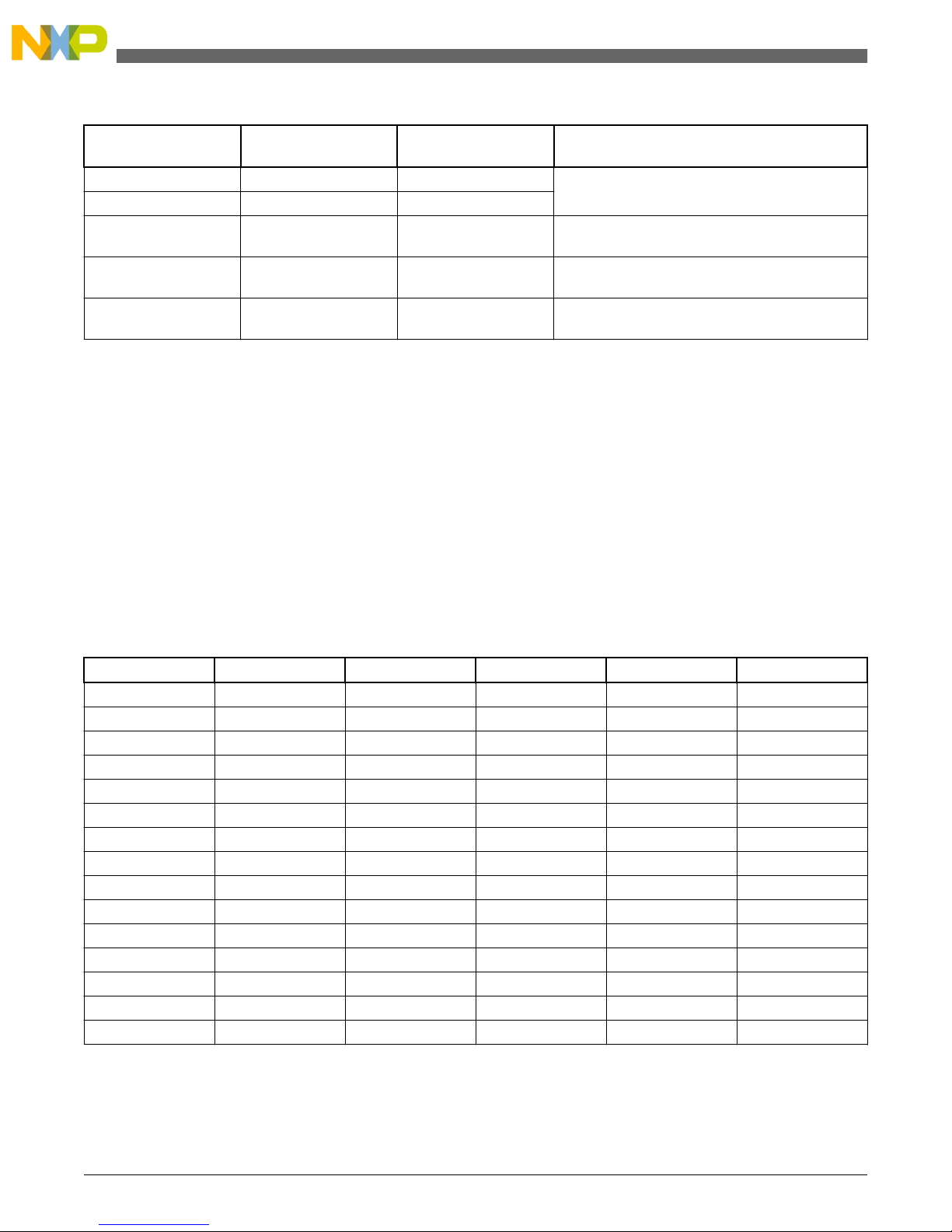
Table 1. Automotive Power Architecture MCU technologies
Family Manufacturing
technology
Transistor geometry Cores used
MPC555 CDR1 350 nm
1
RCPU (Automotive RISC)
MPC56x Family CDR3 250 nm
2
Qorivva MPC55xx
Family
HiP7 120 nm e200z0, e200z1, e200z3, e200z6
Qorivva MPC56xx
Family
c90 90 nm e200z0, e200z3, e200z4, e200z6, e200z7
Qorivva MPC57xx
Family
c55 55 nm e200z0, e200z2, e200z4, e200z7
1. 0.35 micron
2. 0.25 micron
1.1 MPC57xx core instantiations
Many of the different devices in the MPC57xx family have a varying number of cores, including devices with different types
of cores. The following table shows the cores that are instantiated on the different devices in the family. In addition, it shows
the core that debuggers can access after reset with a blank flash (or when a valid reset configuration is not programmed into
the flash). The table also shows whether any of the cores has the option of enabling a lock-step core. On this generation of
MCUs, the lock-step core cannot be used as an independent core, it can only be enabled as a lock-step core. The lock-step
core can be disabled to save power, however, this is not a significant amount of power.
Table 2. MPC57xx core summary
Device Revision Core 0 Core 1 Core 2 Lock-Step core
1
MPC5726L 1
2
e200z215An3 — — —
MPC5744K 1
3
e200z420n3 — e200z225n3
4
Core 0 (e200z419)
MPC5744K 2
2
e200z410Dn3 — e200z225Bn3
4
Core 0 (e200z409)
MPC5744P 1
3
e200z4201n3 — — Core 0 (e200z419)
MPC5744P 2 e200z4251n3 — — Core 0 (e200z424)
MPC5746M 1.0/1.1
3
e200z420n3 e200z420n3 e200z425n3
4
Core 0 (e200z419)
MPC5746M 2 e200z410n3 e200z410n3 e200z425Bn3
4
Core 0 (e200z409)
Future device 1 1
3
e200z425n3 e200z425n3
4
— Core 0 (e200z424)
Future device 1 2 e200z425n3 e200z425n3
4
— Core 0 (e200z424)
MPC5748G 1 e200z4204n3
4
e200z4204n3 e200z210n3 —
MPC5775K 1/1.1
3
e200z4201n3 e200z7260n3 e200z7260n3 Core 0 (e200z419)
MPC5775K 2 e200z4201n3 e200z7260n3 e200z7260n3 Core 0 (e200z419)
Future device 2 1 e200z759n3
4
e200z759n3 — Core 1 (e200z758)
MPC5777M 1
3
e200z720n3 e200z720n3 e200z425Bn3
4
Core 0 (e200z719)
MPC5777M 2 e200z710n3 e200z710n3 e200z425Bn3
4
Core 0 (e200z709)
1. This column shows which core the lock-step core is associated with.
2. This device will not be supported by Freescale.
3. This revision is not intended for production.
Introduction
Qorivva MPC57xx e200zx Core Differences, Rev 0, 10/2013
2 Freescale Semiconductor, Inc.
Page 3
4. Initial default boot core that executes code from the Boot Assist Flash (BAF). Debuggers have access to this core initially
as well.
2 Differences between MPC57xx e200zx cores
The second major generation of the e200zx cores has minor variations for different devices. The following sections show all
of the devices in the MPC57xx family and the variations of the cores used in each device (and version). The core options
have been divided into three sections:
• Core instruction set and execution options (signal processing instruction options, saturated math instructions, floating
point type options, instruction issue option, lock-step option etc.).
• Core bus interface options (memory protection options, end-to-end error correction code options, crossbar bus width,
local memory options, and cache options)
• Core debug options (Nexus class, timestamp option, trace port width, and whether it has the fixed JTAG Nexus register
access sequence)
The tables in the following sections are arranged by core complexity. The e200z210 is the "simplest" core (feature-wise) and
with the e200z759 being the most complex.
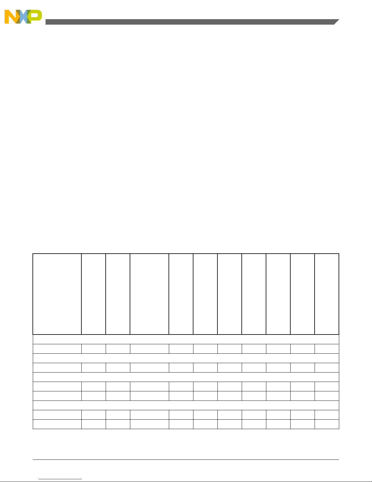
2.1 e200zx core execution options
The first set of options that are available to be integrated into the cores instantiated into a particular MCU directly affect the
cores, including what instructions are supported and how the instructions execute. These options are shown in the following
table, then each of the options is explained in more detail.
Table 3. e200zx cores instruction differences
Device
Revision
Instantiation
Core Name
Book E
Dual Issue
Lockstep
General Purpose Registers
Signal Processing
Saturation
Floating Point
e200z210 based cores
MPC5748G 1.0 Core 2 e200z210n3 No Single No 32x32 No No No
e200z215 based cores
MPC5726L 1.0 Core 01e200z215An3 No Single No 32x32 No No Scalar
e200z225 based cores
MPC5744K 1.0 Core 21e200z225n3 No Single No 32x32 LSP No Scalar
MPC5744K 2.0 Core 21e200z225Bn3 No Single No 32x32 LSP Yes Scalar
e200z410 based cores
MPC5746M 2.0 Core 0/1 e200z410n3 No Single Delayed 32x32 No Yes Scalar
MPC5744K 2.0 Core 0 e200z410Dn3 No Single Delayed 32x32 No Yes Scalar
Table continues on the next page...
Differences between MPC57xx e200zx cores
Qorivva MPC57xx e200zx Core Differences, Rev 0, 10/2013
Freescale Semiconductor, Inc. 3
Page 4
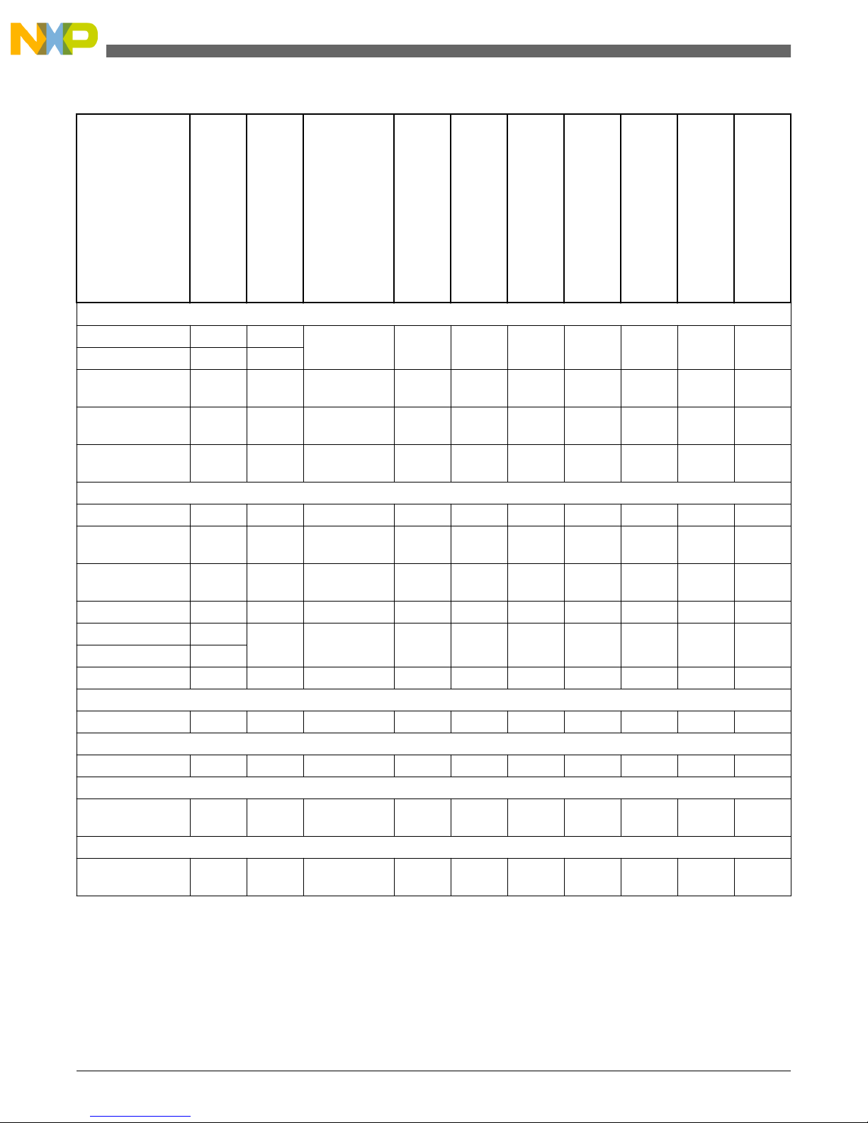
Table 3. e200zx cores instruction differences (continued)
Device
Revision
Instantiation
Core Name
Book E
Dual Issue
Lockstep
General Purpose Registers
Signal Processing
Saturation
Floating Point
e200z420 based cores
MPC5744K 1.0 Core 0 e200z420n3 No Dual Delay
ver.
32x32 No No Scalar
MPC5746M 1.0/1.1 Core 0/1
MPC5744P 1.0 Core 0 e200z4201n3 No Dual Delay
ver.
32x32 No No Scalar
MPC5775K 1.0/1.1/
2.0
Core 0 e200z4201n3 No Dual Delay
ver.
32x32 No No Scalar
MPC5748G 1.0 Core
01/1
e200z4204n3 No Dual No 32x32 No No Scalar
e200z425 based cores
MPC5746M 1.0 Core 21e200z425n3 No Dual No 32x32 LSP No Scalar
Future device 1 1.0 Core
0/1
1
e200z425n3 No Dual Delayed 32x32 LSP No Scalar
Future device 1 2.0 Core
0/1
1
e200z425n3 No Dual Delayed 32x32 LSP Yes Scalar
MPC5777M 1.0 Core 21e200z425Bn3 No Dual No 32x32 LSP No Scalar
MPC5746M 2.0 Core 21e200z425Bn3 No Dual No 32x32 LSP Yes Scalar
MPC5777M 2.0
MPC5744P 2.0 Core 0 e200z4251n3 No Dual Delayed 32x32 LSP No Scalar
e200z710 based cores
MPC5777M 2.0 Core 0/1 e200z710n3 No Single Delayed 32x32 No Yes Scalar
e200z720 based cores
MPC5777M 1.0 Core 0/1 e200z720n3 No Dual Delayed 32x32 No No Scalar
e200z7260 based cores
MPC5775K 1.0/1.1/
2.0
Core 1/2 e200z7260n3 No Dual No 32x64 SPE2 No Vector
e200z759 based cores
Future device 2 1.0 Core
0/1
1
e200z759n3 Yes Dual Delayed 32x64 SPE1.1 No Vector
1. Initial boot core.
Book E Support - Previous e200z3 through e200z7 cores supported both the Power Architecture Book E instruction set and
a more size efficient Variable Length Encoded (VLE) instruction set. The previous e200z0 cores used on some of the
MPC5500 and MPC5600 devices supported only the VLE instruction set. Most of new MPC57xx devices support only the
VLE instruction set, however, there is at least one device planned in the future that will support the full Book E instruction
set.
Differences between MPC57xx e200zx cores
Qorivva MPC57xx e200zx Core Differences, Rev 0, 10/2013
4 Freescale Semiconductor, Inc.
Page 5

Dual Issue - Some versions of the cores can issue two instructions and execute two instructions at a time. Other versions of
the core will only execute a single instruction at a time. There are limitations of the instructions that can execute
concurrently. Each core in an MCU could be defined as either dual- or single-issue variation for a particular MCU.
Lock-step Type - For safety applications, two cores execute instructions in parallel and compare the results to identify errors
in the processor core. To reduce current requirements of the two cores running in parallel, one of the cores can be delayed by
one clock. This spreads the peak current requirements of the core. Not all cores support the lock-step option. In the previous
MPC56xx Family, the cores implemented a true lock-step where the two lock-step cores execute completely in parallel, with
no delay.
General Purpose Registers - Although all of the e200zx cores are 32-bit Power Architecture cores, some versions of the
cores support 64-bit registers that can be used by the Signal Processing Engine (SPE) Auxiliary Processing Unit (APU). Not
all devices support the SPE APU.
Signal Processing Instruction support - There are several options for signal processing extensions to the core, either the
Lightweight Signal Processing Unit or the Signal Processing Extension. These are shown in the following table. Some cores
do not support any signal processing instructions.
Table 4. Signal Processing instruction options
Signal Processing Instructions Version Description
Lightweight Signal Processing Unit
(LSP)
1 The Lightweight Signal Processing Unit (LSP) supports a limited
number of basic math instructions to speed digital signal processing
algorithms.
Signal Processing Extension
(SPE)
1.1 The Signal Processing Engine (SPE) Auxiliary Processing Unit
supports a full range of instructions for digital signal processing
algorithms. There are currently two major versions of the SPE (1.1 and
2.1) that are supported on the MPC57xx devices.
2
No signal processing instructions — Some core variations do not include any type of signal processing
extensions.
Saturation Instruction Support - To better support AutoSAR math functions, saturated math instructions are supported on
some variations/versions of the cores. This allows optimization of some AutoSAR system calls to a single instruction.
Floating Point - Basic floating point instructions are supported on some variations of the cores. These can be defined as part
of the base Power Architecture core. Either scalar or vector floating point options are supported. Vector mode is implemented
in the SPE APU.
2.2 e200zx bus interface and memory options
The cores interface to the rest of the system through a bus interface. The majority of the e200zx cores support a dual bus
structure (Harvard architecture) with a separate instruction fetch bus and a load/store bus.
The following table shows the differences between the e200z cores in regards to the cache sizes, local memory sizes, and bus
interface and control.
Table 5. e200zx cores bus interface and memory options
Device
Revision
Instantiation
Core Name
MPU
e2eECC
XBAR Bus
DTCM
ITCM
D-cache
I-cache
e200z210 based cores
Table continues on the next page...
Differences between MPC57xx e200zx cores
Qorivva MPC57xx e200zx Core Differences, Rev 0, 10/2013
Freescale Semiconductor, Inc. 5
Page 6

Table 5. e200zx cores bus interface and memory options (continued)
Device
Revision
Instantiation
Core Name
MPU
e2eECC
XBAR Bus
DTCM
ITCM
D-cache
I-cache
MPC5748G 1.0 Core 0 e200z210n3 No Yes 64I/64D No No No No
e200z215 based cores
MPC5726L 1.0 Core 0 e200z215An3 No No 32I/32D No No No No
e200z225 based cores
MPC5744K 1.0 Core 2 e200z225n3 8 Yes 64I/64D 48K 16K No No
MPC5744K 2.0 Core 2 e200z225Bn3 8 Yes 64I/32D 48K 16K No No
e200z420 based cores
MPC5746M 2.0 Core 0/1 e200z410n3 24 Yes 64I/64D 64K 16K 4K 8K
MPC5744K 2.0 Core 0 e200z410Dn324 Yes 64I/64D 64K 16K 2K 4K
e200z420 based cores
MPC5744K 1.0/1.1 Core 0 e200z420n3 24 Yes 64I/64D 64K 16K 4K 8K
MPC5746M Core 0/1
MPC5744P 1.0 Core 0 e200z4201n3 24 Yes 64I/64D 64K No 4K 8K
MPC5775K 1.0/1.1/
2.0
Core 2 e200z4201n3 24 Yes 64I/64D 64K No 4K 8K
MPC5748G 1.0 Core 1/2 e200z4204n3 No Yes 64I/64D No No 4K 8K
e200z425 based cores
MPC5746M 1.0 Core 2 e200z425n3 24 Yes 64I/64D 32K 16K No 8K
Future device 1 1.0 Core 0/1 e200z425n3 24 Yes 64I/64D 32K 16K No 8K
Future device 1 2.0 Core 0/1 e200z425n3 24 Yes 64I/64D 32K 16K No 8K
MPC5777M 1.0 Core 2 e200z425Bn3 24 Yes 64I/32D 64K 16K No 8K
MPC5746M 2.0 Core 2 e200z425Bn3 24 Yes 64I/32D 64K 16K No 8K
MPC5777M 2.0
MPC5744P 2.0 Core 0 e200z4251n3 24 Yes 64I/64D 64K No 4K 8K
e200z710 based cores
MPC5777M 2.0 Core 0/1 e200z710n3 24 Yes 64I/64D 64K 16K 4K 16K
e200z720 based cores
MPC5777M 1.0 Core 0/1 e200z720n3 24 Yes 64I/64D 64K 16K 4K 16K
e200z7260 based cores
MPC5775K 1.0/1.1/
2.0
Core 1/2 e200z7260n3 24 Yes 64I/64D 64K No 16K 16K
e200z759 based cores
Future device 2 1.0 Core 0/1 e200z759n3 MMU No 64I/64D No No 16K 16K
Memory Protection Unit (MPU) - The Memory Protection Unit (MPU) allows memory regions to be protected from being
accessed by certain cores, protected from being modified by certain cores, protected from core execution, for enabling or
disabling of being cached, and for other safety protection features.
Differences between MPC57xx e200zx cores
Qorivva MPC57xx e200zx Core Differences, Rev 0, 10/2013
6 Freescale Semiconductor, Inc.
Page 7

Memory Management Unit (MMU) - The Memory Management Unit is similar to the Memory Protection unit in that it
allows memory regions to be protected from being accessed by certain cores, protected from being modified, and for
enabling/disabling of the cache for that memory region. However, it also supports the capability of remapping a logical (or
virtual) memory address into a physical hardware memory address, including the capability to map addresses based on a
Process ID. The MMU is much more complicated than the MPU, this is only a brief summary of the MMU capabilities. For
more information about the MMU, see a core reference manual or device reference manual that supports the MMU.
End-to-End Error Correction Coding (e2eECC) - End-to-end (e2e) Error Correction Coding (ECC) provides an additional
layer of safety by including ECC on all bus transactions. The ECC for the transfer is generated on the transmitting end of the
transaction and checked at the receiving end. e2eECC is an optional feature that can be implemented with the core and
system interfaces.
Cross-Bar (XBAR) interface - In general, the e200zx cores have traditionally implemented a 64-bit bus interface to the
Cross-Bar switch. On the newer e200zx cores, the instruction bus interface remains 64-bit, however, the data load/store bus
on some versions of the cores are implemented with a 32-bit interface to save power and die area (cost).
Local Data Memory (DTCM) - Some cores support a fast local data memory (SRAM). This is sometimes referred to as a
tightly coupled memory (DTCM). The size of this SRAM is definable for a given core variant. Not all devices implement
local memory. The local data memory allows for fast access of variables that are required frequently by a single core.
Local Instruction Memory (ITCM) - Some cores support a fast local instruction memory (SRAM). This is sometimes
referred to as a tightly coupled memory (ITCM). The size of this SRAM is definable for a given core variant. Not all devices
implement local memory. The local instruction memory can be loaded with frequently executed software routines, this is
similar to the concept of locking some regions of cache for frequently used subroutines or functions.
Data Cache (D-Cache) - Data cache allows fast access to recently used data from the load/store bus from memory space
outside of the core complex, typically the device internal flash or external1 (to the device) memory. Different sizes of DCache can be instantiated (as defined for a device) in a particular core.
Instruction Cache (I-Cache) - Instruction cache allows fast access to recently loaded instructions from memory (typically
flash). Different sizes of I-Cache can be instantiated (as defined for a device) in a particular core.
2.3 e200zx debug options
As with other features of the core, the debug options can be determined by the definition of the device requirements. These
allow different kinds of support depending on the requirements of the overall system. These options are shown in the
following table. Each of the options is then explained.
Table 6. e200zx cores debug feature options
Device
Revision
Instantiation
Core Name
Nexus class support
Timestamp
Nexus Port Width (MDO)
JTAG Nexus State
Machine Reset
DQM DQTAG packet type
e200z210 based cores
Table continues on the next page...
1. Not all devices support an external bus.
Differences between MPC57xx e200zx cores
Qorivva MPC57xx e200zx Core Differences, Rev 0, 10/2013
Freescale Semiconductor, Inc. 7
Page 8

Table 6. e200zx cores debug feature options (continued)
Device
Revision
Instantiation
Core Name
Nexus class support
Timestamp
Nexus Port Width (MDO)
JTAG Nexus State
Machine Reset
DQM DQTAG packet type
MPC5748G 1.0 Core 2 e200z210n3 3+ Yes
(unbuffere
d)
16 or 12 Fixed Fixed
e200z215 based cores
MPC5726L 1.0 Core 0 e200z215An3 3+ No 30 Fixed Fixed
e200z225 based cores
MPC5744K 1.0 Core 2 e200z225n3 3+ No 30 Fixed Fixed
MPC5744K 2.0 Core 2 e200z225Bn3 3+ Yes
(unbuffere
d)
30 Fixed Fixed
e200z410 based cores
MPC5746M 2.0 Core 0/1 e200z410n3 3+ Yes
(unbuffere
d)
30 Fixed Fixed
MPC5744K 2.0 Core 0 e200z410Dn3 3+ Yes
(unbuffere
d)
30 Fixed Fixed
e200z420 based cores
MPC5744K 1.0 Core 0 e200z420n3 3+ No 30 — Variable
MPC5746M 1.0/1.1 Core 0/1
MPC5744P 1.0 Core 0 e200z4201n3 3+ No 30 or 4 Fixed Fixed
MPC5775K 1.0/1.1/
2.0
Core 0 e200z4201n3 3+ Yes
(buffered)
30 or 16 Fixed Fixed
MPC5748G 1.0 Core 1/2 e200z4204n3 3+ Yes
(buffered)
16 or 12 Fixed Fixed
e200z425 based cores
MPC5746M 1.0 Core 2 e200z425n3 3+ No 30 — Variable
Future device 1 1.0 Core 0/1 e200z425n3 3+ No 30 or 4
1
Fixed Fixed
Future device 1 2.0 Core 0/1 e200z425n3 3+ No 30 or 4
1
Fixed Fixed
MPC5777M 1.0 Core 2 e200z425Bn3 3+ No 30 Fixed Fixed
MPC5746M 2.0 Core 2 e200z425Bn3 3+ Yes
(unbuffere
d)
30 Fixed Fixed
MPC5777M 2.0 Core 2
MPC5744P 2.0 Core 0 e200z4251n3 3+ No 30 or 4 Fixed Fixed
e200z710 based cores
MPC5777M 2.0 Core 0/1 e200z710n3 3+ No
2
30 Fixed Fixed
Table continues on the next page...
Differences between MPC57xx e200zx cores
Qorivva MPC57xx e200zx Core Differences, Rev 0, 10/2013
8 Freescale Semiconductor, Inc.
Page 9

Table 6. e200zx cores debug feature options (continued)
Device
Revision
Instantiation
Core Name
Nexus class support
Timestamp
Nexus Port Width (MDO)
JTAG Nexus State
Machine Reset
DQM DQTAG packet type
e200z720 based cores
MPC5777M 1.0 Core 0/1 e200z720n3 3+ No 30 Fixed Fixed
e200z7260 based cores
MPC5775K 1.0/1.1/
2.0
Core 1/2 e200z7260n3 3+ Yes
(buffered)
30 or 16
3
Fixed Fixed
e200z759 based cores
Future device 2 1.0 Core 0/1 e200z759n3 3+ No 16 or 12 Fixed Variable
1. Although a 4-bit parallel Nexus MDO port is implemented in the core, it is not possible to select this mode in the Nexus
Aurora Router (NAR).
2. Unbuffered timestamps had been planned for these cores.
3. Although a 16-bit parallel Nexus MDO port can be selected, pins are not available on the package to allow it to be
accessed.
Nexus Class support - The IEEE-ISTO 5001 standard supports multiple "Classes" of support. The e200zx cores can be
instantiated with different levels of support. An overview of the Nexus Class definitions can be found in AN4088
"MPC5500/MPC5600 Nexus Support Overview".
Nexus Timestamp Support - The IEEE-ISTO 5001 standard allows Nexus messages to have timestamps appended to the
message to better track the exact timing of the messages. Timestamps are an optional feature. When implemented on the
e200zx cores, the timestamps can either be implemented as buffered or non-buffered. In general, the unbuffered mode is
implemented on devices with a Nexus Aurora Router (NAR) as the Nexus output controller. Devices that instantiate the
Nexus Port Controller (NPC) use the buffered timestamps. This difference is due to the minimal time that messages spend in
the core Nexus buffers on NAR devices since the NAR implements dedicated input queues from each Nexus client on the
device. However, the NPC only acts as a switch from the output of the individual Nexus clients directly to the Nexus output
port. The NPC implements no buffers for holding messages. On NPC based devices, each client implements the buffers that
hold Nexus messages while other Nexus clients are transmitting their message out of the device.
Table 7. Nexus Timestamp support
Timestamp type Description
Buffered The buffered option appends the timestamp to the Nexus message when the message is
written into the e200zx core Nexus message buffers.
Unbuffered The unbuffered option appends the timestamp to the Nexus message when the message
leaves the core buffers and is transferred to the device level NPC or NAR.
Nexus Port Width - The width of the Nexus Auxiliary port (trace information) is definable for the e200zx core definition.
Typically, a 30-bit Message Data Output port is used when supporting the IEEE-ISTO 5001-2012 high-speed serial Nexus
Aurora port. Smaller sizes are generally used for a parallel Message Data Output Nexus port. Some core variations support
two port widths, while some variations support only a single port width. This is primarily to support either the Nexus Port
Differences between MPC57xx e200zx cores
Qorivva MPC57xx e200zx Core Differences, Rev 0, 10/2013
Freescale Semiconductor, Inc. 9
Page 10

Controller (NPC, used on the previous MPC5500/MPC5600 devices) that supports selection between two different port
widths, and the Nexus Aurora Router (NAR, used on some of the MPC5700 devices) that supports only a single port width.
The port width, along with the port speed, define the maximum bandwidth that is available for trace information.
Table 8. Typical Nexus port width usage
Number of Message Data Outputs Typical use
4 Low-bandwidth parallel Nexus Auxiliary trace port
8 Medium-bandwidth parallel Nexus Auxiliary trace port
1
12 Medium-bandwidth parallel Nexus Auxiliary trace port
16 High-bandwidth parallel Nexus Auxiliary trace port
30 Very high-bandwidth serial Nexus Aurora trace
1. This depends on the number of cores and the Nexus parallel port clock speed.
JTAG Nexus State Machine Reset - In some cases, the Nexus state machine in the e200zx core does not get properly reset
when the JTAG TAP is changed to a different JTAG client (to a different core or other client). Previously, the Nexus JTAG
state machine was reset only if the JTAG IR changed the CMD/DATA. It has been modified to reset the Nexus state machine
anytime the JTAG state machine goes through the UPDATE_IR state.
Data Acquisition Message (DQM) Data Tag (DQTAG) packet type - The Data Tag (DQTAG) packet of the Data
Acquisition Message (DQM) is defined by the IEEE-ISTO 5001 standard as a Fixed length field. Some versions of the cores
incorrectly implement the DQTAG as a Variable length packet instead of the Fixed length field.
Appendix A Revision history
The table below shows the complete revision history of this document.
Table A-1. Revision History
Revision Author Changes
0 Randy Dees Initial customer release.
Qorivva MPC57xx e200zx Core Differences, Rev 0, 10/2013
10 Freescale Semiconductor, Inc.
Page 11

How to Reach Us:
Home Page:
freescale.com
Web Support:
freescale.com/support
Information in this document is provided solely to enable system and
software implementers to use Freescale products. There are no express
or implied copyright licenses granted hereunder to design or fabricate
any integrated circuits based on the information in this document.
Freescale reserves the right to make changes without further notice to
any products herein.
Freescale makes no warranty, representation, or guarantee regarding
the suitability of its products for any particular purpose, nor does
Freescale assume any liability arising out of the application or use of
any product or circuit, and specifically disclaims any and all liability,
including without limitation consequential or incidental damages.
“Typical” parameters that may be provided in Freescale data sheets
and/or specifications can and do vary in different applications, and
actual performance may vary over time. All operating parameters,
including “typicals,” must be validated for each customer application by
customer's technical experts. Freescale does not convey any license
under its patent rights nor the rights of others. Freescale sells products
pursuant to standard terms and conditions of sale, which can be found
at the following address: freescale.com/SalesTermsandConditions.
Freescale, the Freescale logo, and Qorivva are trademarks of Freescale
Semiconductor, Inc., Reg. U.S. Pat. & Tm. Off. SafeAssure and
SafeAssure logo are trademarks of Freescale Semiconductor, Inc. All
other product or service names are the property of their respective
owners.
© 2013 Freescale Semiconductor, Inc.
Document Number AN4802
Revision 0, 10/2013
 Loading...