

Page 1

MPC5777C Reference Manual
Addendum
Supports maskset 2N45H
Document Number: MPC5777CRMAD
Rev. 1, 12/2015
Page 2

MPC5777C Reference Manual Addendum, Rev. 1, 12/2015
2 Freescale Semiconductor, Inc.
Page 3

Contents
Section number Title Page
Chapter 1
Preface
1.1 Overview...........................................................................................................................................................................7
1.2 Device versions.................................................................................................................................................................7
1.3 Audience...........................................................................................................................................................................8
1.4 Document organization.....................................................................................................................................................8
1.5 Conventions......................................................................................................................................................................8
1.5.1 Numbering systems..............................................................................................................................................8
1.5.2 Typographic notation...........................................................................................................................................9
1.5.3 Special terms........................................................................................................................................................9
1.6 References.........................................................................................................................................................................10
Chapter 2
Platform Configuration Module (PCM)
2.1 PCM memory map and register descriptions....................................................................................................................11
2.1.1 FEC Burst Optimization Master Control Register (PCM_FBOMCR)................................................................12
2.1.2 Bus Bridge Configuration Register 1 (PCM_IAHB_BE1)..................................................................................13
2.1.3 Bus Bridge Configuration Register 2 (PCM_IAHB_BE2)..................................................................................16
Chapter 3
Modular CAN (M_CAN)
3.1 Chip-specific M_CAN information..................................................................................................................................19
3.1.1 M_CAN Message RAM allocation......................................................................................................................19
3.1.2 Introduction..........................................................................................................................................................19
3.1.3 Functional Description.........................................................................................................................................20
3.1.4 External Signals...................................................................................................................................................22
3.2 Overview...........................................................................................................................................................................23
3.2.1 Features................................................................................................................................................................23
3.2.2 Block Diagram.....................................................................................................................................................24
3.2.3 Dual Clock Sources..............................................................................................................................................26
MPC5777C Reference Manual Addendum, Rev. 1, 12/2015
Freescale Semiconductor, Inc. 3
Page 4

Section number Title Page
3.2.4 Dual Interrupt Lines.............................................................................................................................................26
3.3 Memory Map and Register Description............................................................................................................................27
3.3.1 Core Release Register (M_CAN_CREL)............................................................................................................28
3.3.2 Endian Register (M_CAN_ENDN).....................................................................................................................29
3.3.3 Fast Bit Timing and Prescaler Register (M_CAN_FBTP)..................................................................................30
3.3.4 Test Register (M_CAN_TEST)...........................................................................................................................32
3.3.5 RAM Watchdog Register (M_CAN_RWD)........................................................................................................33
3.3.6 CC Control Register (M_CAN_CCCR)..............................................................................................................34
3.3.7 Bit Timing and Prescaler Register (M_CAN_BTP)............................................................................................36
3.3.8 Timestamp Counter Configuration Register (M_CAN_TSCC)..........................................................................38
3.3.9 Timestamp Counter Value Register (M_CAN_TSCV).......................................................................................38
3.3.10 Timeout Counter Configuration Register (M_CAN_TOCC)..............................................................................39
3.3.11 Timeout Counter Value Register (M_CAN_TOCV)...........................................................................................40
3.3.12 Error Counter Register (M_CAN_ECR)..............................................................................................................41
3.3.13 Protocol Status Register (M_CAN_PSR)............................................................................................................42
3.3.14 Interrupt Register (M_CAN_IR)..........................................................................................................................45
3.3.15 Interrupt Enable Register (M_CAN_IE)..............................................................................................................49
3.3.16 Interrupt Line Select Register (M_CAN_ILS).....................................................................................................52
3.3.17 Interrupt Line Enable Register (M_CAN_ILE)...................................................................................................55
3.3.18 Global Filter Configuration Register (M_CAN_GFC)........................................................................................56
3.3.19 Standard ID Filter Configuration Register (M_CAN_SIDFC)............................................................................57
3.3.20 Extended ID Filter Configuration Register (M_CAN_XIDFC)..........................................................................58
3.3.21 Extended ID and Mask Register (M_CAN_XIDAM).........................................................................................59
3.3.22 High Priority Message Status Register (M_CAN_HPMS)..................................................................................59
3.3.23 New Data 1 Register (M_CAN_NDAT1)...........................................................................................................60
3.3.24 New Data 2 Register (M_CAN_NDAT2)...........................................................................................................61
3.3.25 Rx FIFO 0 Configuration Register (M_CAN_RXF0C)......................................................................................61
3.3.26 Rx FIFO 0 Status Register (M_CAN_RXF0S)....................................................................................................62
3.3.27 Rx FIFO 0 Acknowledge Register (M_CAN_RXF0A)......................................................................................63
MPC5777C Reference Manual Addendum, Rev. 1, 12/2015
4 Freescale Semiconductor, Inc.
Page 5

Section number Title Page
3.3.28 Rx Buffer Configuration Register (M_CAN_RXBC).........................................................................................64
3.3.29 Rx FIFO 1 Configuration Register (M_CAN_RXF1C)......................................................................................64
3.3.30 Rx FIFO 1 Status Register (M_CAN_RXF1S)....................................................................................................65
3.3.31 Rx FIFO 1 Acknowledge Register (M_CAN_RXF1A)......................................................................................66
3.3.32 Rx Buffer / FIFO Element Size Configuration Register (M_CAN_RXESC).....................................................67
3.3.33 Tx Buffer Configuration Register (M_CAN_TXBC)..........................................................................................69
3.3.34 Tx FIFO/Queue Status Register (M_CAN_TXFQS)...........................................................................................70
3.3.35 Tx Buffer Element Size Configuration (M_CAN_TXESC)................................................................................71
3.3.36 Tx Buffer Request Pending Register (M_CAN_TXBRP)...................................................................................72
3.3.37 Tx Buffer Add Request Register (M_CAN_TXBAR)........................................................................................73
3.3.38 Tx Buffer Cancellation Request Register (M_CAN_TXBCR)...........................................................................73
3.3.39 Tx Buffer Transmission Occurred Register (M_CAN_TXBTO)........................................................................74
3.3.40 Tx Buffer Cancellation Finished Register (M_CAN_TXBCF)...........................................................................74
3.3.41 Tx Buffer Transmission Interrupt Enable Register (M_CAN_TXBTIE)............................................................75
3.3.42 Tx Buffer Cancellation Finished Interrupt Enable Register (M_CAN_TXBCIE)..............................................75
3.3.43 Tx Event FIFO Configuration Register (M_CAN_TXEFC)...............................................................................76
3.3.44 Tx Event FIFO Status Register (M_CAN_TXEFS)............................................................................................77
3.3.45 Tx Event FIFO Acknowledge Register (M_CAN_TXEFA)...............................................................................78
3.4 Message RAM..................................................................................................................................................................78
3.4.1 Rx Buffer and FIFO Element...............................................................................................................................79
3.4.2 Tx Buffer Element...............................................................................................................................................81
3.4.3 Tx Event FIFO Element.......................................................................................................................................83
3.4.4 Standard Message ID Filter Element...................................................................................................................84
3.4.5 Extended Message ID Filter Element..................................................................................................................85
3.5 Functional Description......................................................................................................................................................87
3.5.1 Operating Modes..................................................................................................................................................87
3.5.2 Timestamp Generation.........................................................................................................................................96
3.5.3 Timeout Counter..................................................................................................................................................97
MPC5777C Reference Manual Addendum, Rev. 1, 12/2015
Freescale Semiconductor, Inc. 5
Page 6

Section number Title Page
3.5.4 Rx Handling.........................................................................................................................................................97
3.5.5 Tx Handling.........................................................................................................................................................108
3.5.6 FIFO Acknowledge Handling..............................................................................................................................114
3.5.7 Interface to DMA Controller................................................................................................................................114
MPC5777C Reference Manual Addendum, Rev. 1, 12/2015
6 Freescale Semiconductor, Inc.
Page 7

Chapter 1
Preface
1.1 Overview
For users of maskset 2N45H, this addendum supplements—and must be used in
conjunction with—the latest version of the MPC5777C Reference Manual. The primary
objective of this document is to define the major differences in functionality of maskset
2N45H from maskset 3N45H for software and hardware developers.
The information in this document is subject to change. As with any technical
documentation, it is the reader’s responsibility to ensure he or she is using the most recent
version of the documentation.
To locate any published errata or updates for this document, visit the Freescale Web site
at http://www.freescale.com.
1.2 Device versions
This document is necessary for users of maskset 2N45H. It describes the functionality
and programming model of maskset 2N45H that differ from maskset 3N45H.
For 2N45H, the body chapters in this addendum replace the corresponding chapters of the
latest MPC5777C Reference Manual (document number MPC5777CRM). Other chapters
in the latest MPC5777C Reference Manual accurately describe 2N45H.
MPC5777C Reference Manual Addendum, Rev. 1, 12/2015
Freescale Semiconductor, Inc. 7
Page 8

Audience
1.3 Audience
This addendum is intended for system software and hardware developers and applications
programmers who want to develop products with maskset 2N45H of the MPC5777C. It is
assumed that the reader understands operating systems, microprocessor system design,
basic principles of software and hardware, and basic details of the Power Architecture®
developed by Freescale.
1.4 Document organization
This document contains two chapters whose content differs from the corresponding
chapters of the MPC5777C Reference Manual:
• Platform Configuration Module (PCM)
• Modular CAN (M_CAN)
These addendum chapters describe the indicated modules for maskset 2N45H. The
corresponding chapters of the MPC5777C Reference Manual describe the indicated
modules for maskset 3N45H.
1.5
Conventions
1.5.1 Numbering systems
The following suffixes identify different numbering systems:
This suffix Identifies a
b Binary number. For example, the binary equivalent of the number 5 is written 101b. In some cases,
binary numbers are shown with the prefix 0b.
d Decimal number. Decimal numbers are followed by this suffix only when the possibility of confusion
exists. In general, decimal numbers are shown without a suffix.
h Hexadecimal number. For example, the hexadecimal equivalent of the number 60 is written 3Ch. In
some cases, hexadecimal numbers are shown with the prefix 0x.
MPC5777C Reference Manual Addendum, Rev. 1, 12/2015
8 Freescale Semiconductor, Inc.
Page 9

Chapter 1 Preface
1.5.2 Typographic notation
The following typographic notation is used throughout this document:
Example Description
placeholder, x Items in italics are placeholders for information that you provide. Italicized text is also used for
the titles of publications and for emphasis. Plain lowercase letters are also used as
placeholders for single letters and numbers.
code
SR[SCM] A mnemonic in brackets represents a named field in a register. This example refers to the
REVNO[6:4], XAD[7:0] Numbers in brackets and separated by a colon represent either:
Fixed-width type indicates text that must be typed exactly as shown. It is used for instruction
mnemonics, directives, symbols, subcommands, parameters, and operators. Fixed-width type
is also used for example code. Instruction mnemonics and directives in text and tables are
shown in all caps; for example, BSR.
Scaling Mode (SCM) field in the Status Register (SR).
• A subset of a register's named field
For example, REVNO[6:4] refers to bits 6–4 that are part of the COREREV field that
occupies bits 6–0 of the REVNO register.
• A continuous range of individual signals of a bus
For example, XAD[7:0] refers to signals 7–0 of the XAD bus.
1.5.3 Special terms
The following terms have special meanings:
Term Meaning
asserted Refers to the state of a signal as follows:
• An active-high signal is asserted when high (1).
• An active-low signal is asserted when low (0).
deasserted Refers to the state of a signal as follows:
• An active-high signal is deasserted when low (0).
• An active-low signal is deasserted when high (1).
In some cases, deasserted signals are described as negated.
reserved Refers to a memory space, register, field, or programming setting. Writes to a reserved location can
result in unpredictable functionality or behavior.
• Do not modify the default value of a reserved programming setting, such as the reset value of
a reserved register field.
• Consider undefined locations in memory to be reserved.
w1c Write 1 to clear: Refers to a register bitfield that must be written as 1 to be "cleared."
MPC5777C Reference Manual Addendum, Rev. 1, 12/2015
Freescale Semiconductor, Inc. 9
Page 10

References
1.6 References
This addendum must be used in conjunction with the latest version of the MPC5777C
Reference Manual (document number MPC5777CRM).
In addition, the following documents provide information about the operation of the
MPC5777C:
• MPC5777C Data Sheet (document number MPC5777C)
• e200z759n3 Core Reference Manual (document number e200z759n3CRM),
available at www.freescale.com
• Safety Manual for MPC5777C (document number MPC5777CSM)
• IEEE-ISTO 5001-2003 Standard for a Global Embedded Processor Interface (Nexus)
• IEEE 1149.1-2001 standard - IEEE Standard Test Access Port and Boundary-Scan
Architecture
• Power Architecture Book E V1.0, available at www.freescale.com: http://
www.freescale.com/files/32bit/doc/user_guide/BOOK_EUM.pdf
MPC5777C Reference Manual Addendum, Rev. 1, 12/2015
10 Freescale Semiconductor, Inc.
Page 11

Chapter 2
Platform Configuration Module (PCM)
2.1 PCM memory map and register descriptions
The Platform Configuration Module contains three miscellaneous configuration registers
for the chip. Currently, the configuration registers are related to the operation of the FEC
and intelligent bus bridging gasket. The module is mapped to AIPS_0 (PBRIDGE_B) onplatform slot 27 with a base address of FFF6_C000h.
NOTE
These registers can be accessed only in supervisor mode.
PCM memory map
Address
offset (hex)
0
4 Bus Bridge Configuration Register 1 (PCM_IAHB_BE1) 32 R/W 0707_0707h 2.1.2/13
8 Bus Bridge Configuration Register 2 (PCM_IAHB_BE2) 32 R/W 0707_0707h 2.1.3/16
FEC Burst Optimization Master Control Register
(PCM_FBOMCR)
Register name
Width
(in bits)
Access Reset value
32 R/W 0000_0000h 2.1.1/12
Section/
page
MPC5777C Reference Manual Addendum, Rev. 1, 12/2015
Freescale Semiconductor, Inc. 11
Page 12

PCM memory map and register descriptions
2.1.1 FEC Burst Optimization Master Control Register
(PCM_FBOMCR)
This register controls FEC burst optimization behavior on the system bus.
Address: 0h base + 0h offset = 0h
Bit 0 1 2 3 4 5 6 7 8 9 10 11 12 13 14 15
R
W
Reset
Reset
0 0 0 0 0 0 0 0 0 0 0 0 0 0 0 0
16 17 18 19 20 21 22 23 24 25 26 27 28 29 30 31
Bit
R
W
0 0 0 0 0 0 0 0 0 0 0 0 0 0 0 0
0
RBEN FXSBE[7:0]
WBEN
ACCERR
PCM_FBOMCR field descriptions
Field Description
0–20
Reserved
21
ACCERR
This field is reserved.
This read-only field is reserved and always has the value 0.
Accumulate Error
This field determines whether an error response for the first half of the write burst is accumulated to the
second half of the write burst or discarded. To complete the burst, the FEC interface to the system bus
responds by indicating that the first half of the burst completed without error before it actually writes the
data so that it can fetch the second half of the write data from the FIFO. When actually written onto the
system bus, the first half of the write burst can have an error. Because this half initially responded without
an error to the FIFO, the error is discarded or accumulated with the error response for the second half of
the burst.
0
0 Any error to the first half of the write burst is discarded.
1 Any actual error response to the first half of the write burst is accumulated in the second half's
response. In other words, an error response to the first half is seen in the response to the second half,
even if the second half does not contain an error.
22
WBEN
23
RBEN
Global write burst enable to XBAR slave port designated by FXSBEn
0 Write bursting to all XBAR slave ports is disabled.
1 Write bursting is enabled to any XBAR slave port whose FXSBEn bit is 1.
Global read burst enable from XBAR slave port designated by FXSBEn
0 Read bursting from all XBAR slave ports is disabled.
1 Read bursting is enabled from any XBAR slave port whose FXSBEn bit is 1.
Table continues on the next page...
MPC5777C Reference Manual Addendum, Rev. 1, 12/2015
12 Freescale Semiconductor, Inc.
Page 13

PCM_FBOMCR field descriptions (continued)
Field Description
24–31
FXSBE[7:0]
FEC XBAR slave burst enable
This field enables bursting by the FEC interface to the XBAR slave port controlled by each FXSBEn bit.
• When a particular FXSBEn bit is 1, the XBAR slave port enabled by that bit can support the bursts
allowed by RBEN and WBEN. RBEN enables read bursts from the XBAR slave port, and WBEN
enables write bursts to the XBAR slave port.
• When a particular FXSBEn bit is 0, the FEC interface does not burst to the XBAR slave port
controlled by that FXSBEn bit.
FXSBEn assignments to XBAR slave ports are as follows:
FXSBE0 = Flash memory
FXSBE1 = EBI
FXSBE2 = RAM
FXSBE3 = reserved
FXSBE4 = reserved
FXSBE5 = reserved
FXSBE6 = AIPS_1 (PBRIDGE_A)
FXSBE7 = AIPS_0 (PBRIDGE_B)
Chapter 2 Platform Configuration Module (PCM)
2.1.2 Bus Bridge Configuration Register 1 (PCM_IAHB_BE1)
Address: 0h base + 4h offset = 4h
Bit 0 1 2 3 4 5 6 7 8 9 10 11 12 13 14 15
R
W
Reset
Reset
0 0 0 0 0 1 1 1 0 0 0 0 0 1 1 1
16 17 18 19 20 21 22 23 24 25 26 27 28 29 30 31
Bit
R
W
0 0 0 0 0 1 1 1 0 0 0 0 0 1 1 1
Field Description
0–4
Reserved
0
D
D
D
PRE_CORE1_
BRE_CORE1_
BWE_CORE1_
0
D
D
D
PRE_CORE0_
BRE_CORE0_
BWE_CORE0_
PCM_IAHB_BE1 field descriptions
This field is reserved.
This read-only field is reserved and always has the value 0.
0
PRE_CORE1_I
0
PRE_CORE0_I
I
BWE_CORE1_
BRE_CORE1_I
I
BWE_CORE0_
BRE_CORE0_I
Table continues on the next page...
MPC5777C Reference Manual Addendum, Rev. 1, 12/2015
Freescale Semiconductor, Inc. 13
Page 14

PCM memory map and register descriptions
PCM_IAHB_BE1 field descriptions (continued)
Field Description
5
PRE_CORE1_D
6
BRE_CORE1_D
7
BWE_CORE1_D
8–12
Reserved
13
PRE_CORE1_I
Pending Read Enable Core1 Data
This bit controls the bus gasket’s handling of pending read transactions.
0 Pending reads are disabled.
1 Pending reads are enabled.
Burst Read Enable Core1 Data
This bit controls the bus gasket’s handling of burst read transactions.
0 Burst reads are converted into a series of single transactions on the slave side of the gasket.
1 Burst reads are optimized for best system performance.
Burst Write Enable Core1 Data
This bit controls the bus gasket’s handling of burst write transactions.
0 Burst writes are converted into a series of single transactions on the slave side of the gasket.
1 Burst writes are optimized for best system performance. Note this setting treats writes as “imprecise”
such that an error response on any beat of the burst is reported on the last beat.
This field is reserved.
This read-only field is reserved and always has the value 0.
Pending Read Enable Core1 Instruction
This bit controls the bus gasket’s handling of pending read transactions.
14
BRE_CORE1_I
15
BWE_CORE1_I
16–20
Reserved
21
PRE_CORE0_D
22
BRE_CORE0_D
0 Pending reads are disabled.
1 Pending reads are enabled.
Burst Read Enable Core1 Instruction
This bit controls the bus gasket’s handling of burst read transactions.
0 Burst reads are converted into a series of single transactions on the slave side of the gasket.
1 Burst reads are optimized for best system performance.
Burst Write Enable Core1 Instruction
This bit controls the bus gasket’s handling of burst write transactions.
0 Burst writes are converted into a series of single transactions on the slave side of the gasket.
1 Burst writes are optimized for best system performance. Note this setting treats writes as “imprecise”
such that an error response on any beat of the burst is reported on the last beat.
This field is reserved.
This read-only field is reserved and always has the value 0.
Pending Read Enable Core0 Data
This bit controls the bus gasket’s handling of pending read transactions.
0 Pending reads are disabled
1 Pending reads are enabled.
Burst Read Enable Core0 Data
This bit controls the bus gasket’s handling of burst read transactions.
Table continues on the next page...
MPC5777C Reference Manual Addendum, Rev. 1, 12/2015
14 Freescale Semiconductor, Inc.
Page 15

PCM_IAHB_BE1 field descriptions (continued)
Field Description
0 Burst reads are converted into a series of single transactions on the slave side of the gasket.
1 Burst reads are optimized for best system performance.
23
BWE_CORE0_D
24–28
Reserved
29
PRE_CORE0_I
30
BRE_CORE0_I
Burst Write Enable Core0 Data
This bit controls the bus gasket’s handling of burst write transactions.
0 Burst writes are converted into a series of single transactions on the slave side of the gasket.
1 Burst writes are optimized for best system performance. Note this setting treats writes as “imprecise”
such that an error response on any beat of the burst is reported on the last beat.
This field is reserved.
This read-only field is reserved and always has the value 0.
Pending Read Enable Core0 Instruction
This bit controls the bus gasket’s handling of pending read transactions.
0 Pending reads are disabled.
1 Pending reads are enabled.
Burst Read Enable Core0 Instruction
This bit controls the bus gasket’s handling of burst read transactions.
Chapter 2 Platform Configuration Module (PCM)
31
BWE_CORE0_I
0 Burst reads are converted into a series of single transactions on the slave side of the gasket.
1 Burst reads are optimized for best system performance.
Burst Write Enable Core0 Instruction
This bit controls the bus gasket’s handling of burst write transactions.
0 Burst writes are converted into a series of single transactions on the slave side of the gasket.
1 Burst writes are optimized for best system performance. Note this setting treats writes as “imprecise”
such that an error response on any beat of the burst is reported on the last beat.
MPC5777C Reference Manual Addendum, Rev. 1, 12/2015
Freescale Semiconductor, Inc. 15
Page 16

PCM memory map and register descriptions
2.1.3 Bus Bridge Configuration Register 2 (PCM_IAHB_BE2)
Address: 0h base + 8h offset = 8h
Bit 0 1 2 3 4 5 6 7 8 9 10 11 12 13 14 15
Reset
Bit
Reset
R
W
0 0 0 0 0 1 1 1 0 0 0 0 0 1 1 1
16 17 18 19 20 21 22 23 24 25 26 27 28 29 30 31
R
W
0 0 0 0 0 1 1 1 0 0 0 0 0 1 1 1
0
PRE_
BRE_
FEC
FEC
BWE_FEC
0
PRE_DMA_B
BRE_DMA_B
BWE_DMA_B
PCM_IAHB_BE2 field descriptions
Field Description
0–4
Reserved
5
PRE_FEC
6
BRE_FEC
This field is reserved.
This read-only field is reserved and always has the value 0.
Pending Read Enable FEC
This bit controls the bus gasket’s handling of pending read transactions.
0 Pending reads are disabled.
1 Pending reads are enabled.
Burst Read Enable FEC
This bit controls the bus gasket’s handling of burst read transactions.
0
PRE_
M6
BRE_M6
BWE_M6
0
PRE_DMA_A
BRE_DMA_A
BWE_DMA_A
0 Burst reads are converted into a series of single transactions on the slave side of the gasket.
1 Burst reads are optimized for best system performance.
7
Burst Write Enable FEC
BWE_FEC
This bit controls the bus gasket’s handling of burst write transactions.
0 Burst writes are converted into a series of single transactions on the slave side of the gasket.
1 Burst writes are optimized for best system performance. Note this setting treats writes as “imprecise”
such that an error response on any beat of the burst is reported on the last beat.
8–12
Reserved
13
This field is reserved.
This read-only field is reserved and always has the value 0.
Pending Read Enable Master Port 6 Concentrator
PRE_M6
This bit controls the bus gasket’s handling of pending read transactions.
Table continues on the next page...
MPC5777C Reference Manual Addendum, Rev. 1, 12/2015
16 Freescale Semiconductor, Inc.
Page 17

PCM_IAHB_BE2 field descriptions (continued)
Field Description
0 Pending reads are disabled.
1 Pending reads are enabled.
14
BRE_M6
15
BWE_M6
16–20
Reserved
21
PRE_DMA_B
Burst Read Enable Master Port 6 Concentrator
This bit controls the bus gasket’s handling of burst read transactions.
0 Burst reads are converted into a series of single transactions on the slave side of the gasket.
1 Burst reads are optimized for best system performance.
Burst Write Enable Master Port 6 Concentrator
This bit controls the bus gasket’s handling of burst write transactions.
0 Burst writes are converted into a series of single transactions on the slave side of the gasket.
1 Burst writes are optimized for best system performance. Note this setting treats writes as “imprecise”
such that an error response on any beat of the burst is reported on the last beat.
This field is reserved.
This read-only field is reserved and always has the value 0.
Pending Read Enable eDMA_B
This bit controls the bus gasket’s handling of pending read transactions.
Chapter 2 Platform Configuration Module (PCM)
22
BRE_DMA_B
23
BWE_DMA_B
24–28
Reserved
29
PRE_DMA_A
30
BRE_DMA_A
0 Pending reads are disabled
1 Pending reads are enabled.
Burst Read Enable eDMA_B
This bit controls the bus gasket’s handling of burst read transactions.
0 Burst reads are converted into a series of single transactions on the slave side of the gasket.
1 Burst reads are optimized for best system performance.
Burst Write Enable eDMA_B
This bit controls the bus gasket’s handling of burst write transactions.
0 Burst writes are converted into a series of single transactions on the slave side of the gasket.
1 Burst writes are optimized for best system performance. Note this setting treats writes as “imprecise”
such that an error response on any beat of the burst is reported on the last beat.
This field is reserved.
This read-only field is reserved and always has the value 0.
Pending Read Enable eDMA_A
This bit controls the bus gasket’s handling of pending read transactions.
0 Pending reads are disabled.
1 Pending reads are enabled.
Burst Read Enable eDMA_A
This bit controls the bus gasket’s handling of burst read transactions.
0 Burst reads are converted into a series of single transactions on the slave side of the gasket.
1 Burst reads are optimized for best system performance.
Table continues on the next page...
MPC5777C Reference Manual Addendum, Rev. 1, 12/2015
Freescale Semiconductor, Inc. 17
Page 18

PCM memory map and register descriptions
PCM_IAHB_BE2 field descriptions (continued)
Field Description
31
BWE_DMA_A
Burst Write Enable eDMA_A
This bit controls the bus gasket’s handling of burst write transactions.
0 Burst writes are converted into a series of single transactions on the slave side of the gasket.
1 Burst writes are optimized for best system performance. Note this setting treats writes as “imprecise”
such that an error response on any beat of the burst is reported on the last beat.
MPC5777C Reference Manual Addendum, Rev. 1, 12/2015
18 Freescale Semiconductor, Inc.
Page 19

Chapter 3
Modular CAN (M_CAN)
3.1 Chip-specific M_CAN information
3.1.1 M_CAN Message RAM allocation
On this chip, each M_CAN instance can address 1216 words in the Message RAM.
As a result, the Message RAM shared by the two M_CAN instances supports 2432
words, or 9.5 KB.
3.1.2 Introduction
The M_CAN subsystem includes:
• Two M_CAN modules
• A Message RAM controller
The M_CAN subsystem block diagram is shown in the following figure.
MPC5777C Reference Manual Addendum, Rev. 1, 12/2015
Freescale Semiconductor, Inc. 19
Page 20
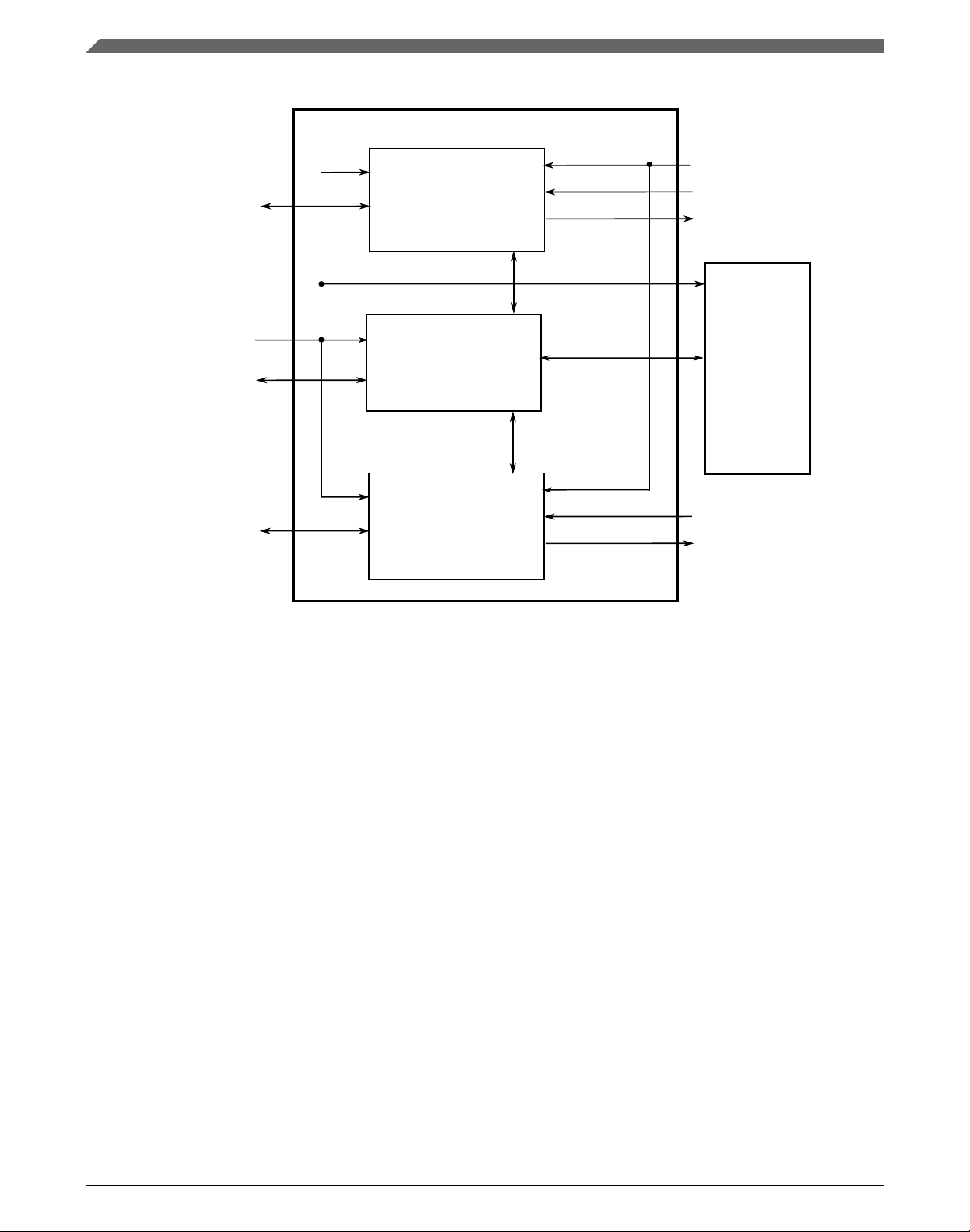
M _C AN_0
host clock
M_CAN_0_Rx
M_CAN_0_Tx
CAN protocol clock
Message RAM
Controller
External
Message
RAM
CPU reads/writes
CPU reads/writes
M_CAN Subsystem
CPU clock*
M _C AN_1
host clock
M_CAN_1_Rx
M_CAN_1_Tx
CPU reads/writes
*Refer to the Clocking chapter for M_CAN clock details.
Chip-specific M_CAN information
Figure 3-1. M_CAN subsystem block diagram
3.1.3 Functional Description
3.1.3.1 Message RAM Controller
The Message RAM Controller has the arbiter for the accesses to the external Message
RAM and the ECC (Error Code Correction) Controller for the external Message RAM
data.
3.1.3.1.1 Message RAM Arbiter
The Message RAM Arbiter is a dynamic round robin arbiter that selects which request is
sent to the external Message RAM. These requests are made by the CPU, M_CAN_0, or
M_CAN_1.
This arbiter ensures:
MPC5777C Reference Manual Addendum, Rev. 1, 12/2015
20 Freescale Semiconductor, Inc.
Page 21

CPU
M_CAN_0
CPU
M_CAN_0
CPU
M_CAN_0
CPU
M_CAN_0
CPU clock
who accesses the
external Message RAM
M_CAN_1 M_CAN_1 M_CAN_1 M_CAN_1
CPU clock
who accesses the
external Message RAM
M_CAN_0 M_CAN_0 M_CAN_0 M_CAN_0
CPU
M_CAN_0
CPU
M_CAN_1
CPU
M_CAN_0
CPU
M_CAN_1
CPU clock
who accesses the
external Message RAM
Chapter 3 Modular CAN (M_CAN)
• 50% bandwidth for CPU accesses to the external Message RAM. The CPU does not
wait for more than one clock cycle to access the external Message RAM (see
examples 1 and 3).
• 50% bandwidth is shared between M_CAN_0 and M_CAN_1 accesses to the
external Message RAM. Each M_CAN waits at least one clock cycle to access the
external Message RAM (see examples 1, 2, and 3).
• If there is no CPU request, all bandwidth is distributed to M_CAN_0 and M_CAN_1
(see example 2).
• If there are no M_CAN_0 and M_CAN_1 requests, all bandwidth is distributed to the
CPU.
• If there are requests from only one M_CAN, the other M_CAN's bandwidth is
distributed to the first M_CAN (see example 1).
The following examples illustrate the dynamic arbiter scheme.
• Example 1: The following figure shows who accesses the external Message RAM
when only CPU and M_CAN_0 try to access to it.
• Example 2: The following figure shows who accesses the external Message RAM
when only M_CAN_0 and M_CAN_1 try to access to it.
• Example 3: The following figure shows who accesses the external Message RAM
when the CPU, M_CAN_0, and M_CAN_1 try to access to it.
The read or write accesses to the external Message RAM use two clock cycles. In the first
clock cycle, the address is available, and in the second, the data is available.
Freescale Semiconductor, Inc. 21
MPC5777C Reference Manual Addendum, Rev. 1, 12/2015
Page 22

Chip-specific M_CAN information
The arbiter has a pseudo address pre-fetching mechanism that allows the data of the
previous access to overlap with the address of the current access. The pseudo address prefetching scheme saves multiple clock cycles when there are multiples accesses to the
external Message RAM.
3.1.3.1.2 ECC Controller
The ECC Controller provides Single Error Correction / Double Error Detection
(SECDED). It guarantees single bit error correction and double bit error detection
(without correction). The SECDED code is not guaranteed to detect more than two bits
with error.
Each 32 data bits of the external Message RAM is associated with 7 ECC bits. If all these
39 bits are zero or one, then it is flagged as non-correctable error.
For writes to the external Message RAM, the ECC bits (7-bit) are calculated using the
data bits (32-bit). The data bits plus ECC bits (39-bit) are written into the specified
memory address. The error detection and correction are performed on the reads from the
external Message RAM.
When an M_CAN accesses the external Message RAM, the ECC bits are calculated by
the ECC Controller and they are sent to this M_CAN.
3.1.3.2 External Message RAM
The external Message RAM supports only 32-bit write and read accesses.
The CPU can access the external Message RAM through the M_CAN subsystem. In this
case, the CPU can do 8/16/32-bit read accesses to the external Message RAM.
3.1.3.3 Transfer Error
The M_CAN subsystem does not report any transfer error.
3.1.4 External Signals
The M_CAN subsystem external signals are shown in the following table.
MPC5777C Reference Manual Addendum, Rev. 1, 12/2015
22 Freescale Semiconductor, Inc.
Page 23

Chapter 3 Modular CAN (M_CAN)
Table 3-1. M_CAN subsystem external signals
Signal name Direction Description
M_CAN_0_Rx input M_CAN_0 CAN Rx signal
M_CAN_0_Tx output M_CAN_0 CAN Tx signal
M_CAN_1_Rx input M_CAN_1 CAN Rx signal
M_CAN_1_Tx output M_CAN_1 CAN Tx signal
3.2 Overview
The M_CAN module is the new CAN Communication Controller IP-module. The
M_CAN performs communication according to ISO11898-1 (Bosch CAN specification
2.0 part A,B) and to Bosch CAN FD specification V1.0. Additional transceiver hardware
is required for connection to the physical layer.
The message storage is intended to be a single- or dual-ported Message RAM outside of
the module. It is connected to the M_CAN via the Generic Master Interface. Depending
on the chosen device, multiple M_CAN controllers can share the same Message RAM.
All functions concerning the handling of messages are implemented by the Rx Handler
and the Tx Handler. The Rx Handler manages message acceptance filtering, the transfer
of received messages from the CAN Core to the Message RAM as well as providing
receive message status information. The Tx Handler is responsible for the transfer of
transmit messages from the Message RAM to the CAN Core as well as providing
transmit status information.
Acceptance filtering is implemented by a combination of up to 128 filter elements where
each one can be configured as a range, as a bit mask, or as a dedicated ID filter.
The M_CAN can be connected to a wide range of Host CPUs via its 8/16/32-bit Generic
Slave Interface. The M_CAN's clock domain concept allows the separation between the
high precision CAN clock and the Host clock, which may be generated by an FM-PLL.
3.2.1 Features
The following are the features of M_CAN.
• Conforms with CAN protocol version 2.0 part A, B and ISO 11898-1
• CAN FD with up to 64 data bytes supported
• CAN Error Logging
MPC5777C Reference Manual Addendum, Rev. 1, 12/2015
Freescale Semiconductor, Inc. 23
Page 24

Overview
• AUTOSAR optimized
• SAE J1939 optimized
• Improved acceptance filtering
• Two configurable Receive FIFOs
• Separate signalling on reception of High Priority Messages
• Up to 64 dedicated Receive Buffers
• Up to 32 dedicated Transmit Buffers
• Configurable Transmit FIFO
• Configurable Transmit Queue
• Configurable Transmit Event FIFO
• Direct Message RAM access for Host CPU
• Multiple M_CANs may share the same Message RAM
• Programmable loop-back test mode
• Maskable module interrupts
• 8/16/32-bit Generic Slave Interface for connection customer-specific Host CPUs
• Two clock domains (CAN clock and Host clock)
• Power-down support
• Debug on CAN support
MPC5777C Reference Manual Addendum, Rev. 1, 12/2015
24 Freescale Semiconductor, Inc.
Page 25
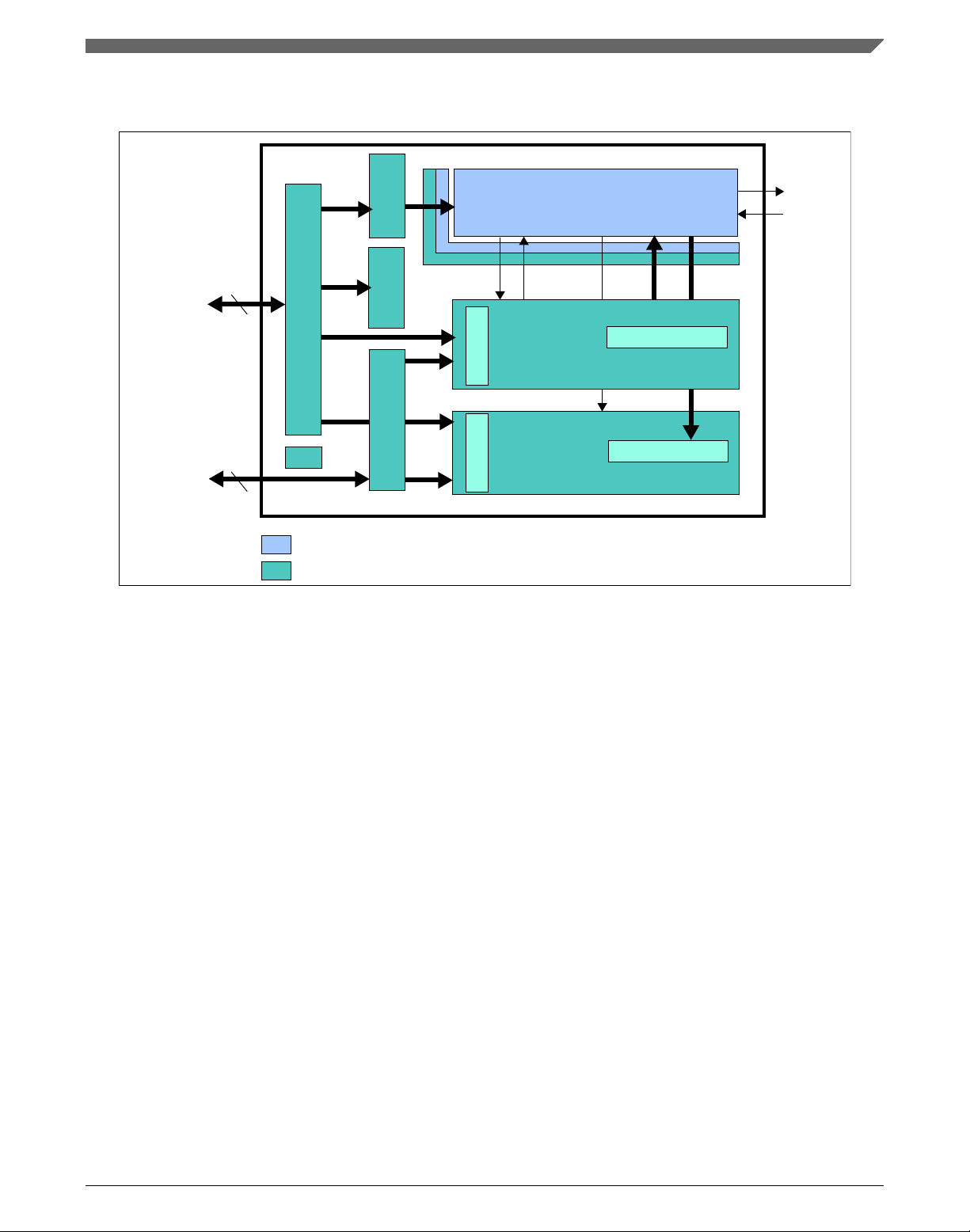
3.2.2 Block Diagram
Timestamp
Cfg and Ctrl
Cfg and Ctrl
Host Clock Domain
Tx Prioritization
Acceptance Filter
8/16/32
Cfg and Ctrl
CAN Clock Domain
Memory IF
M_CAN
Rx Handler
Host IF
Tx Handler
CAN Core
Generic Slave IF
Generic Master IF
Rx_State
Sync
Tx_Req
Tx_State
Clk
32
CAN Tx
CAN
R x
Chapter 3 Modular CAN (M_CAN)
Figure 3-2. M_CAN Block Diagram
• CAN Core: CAN Protocol Controller and Rx/Tx Shift Register. Handles all ISO
11898-1 protocol functions. Supports 11-bit and 29-bit identifiers.
• Sync: Synchronizes signals from the Host clock domain to the CAN clock domain
and vice versa.
• Clk: Synchronizes reset signal to the Host clock domain and to the CAN clock
domain.
• Cfg and Ctrl: CAN Core related configuration and control bits.
• Interrupt and Timestamp: Interrupt control and 16-bit CAN bit time counter for
receive and transmit timestamp generation.
• Tx Handler: Controls the message transfer from the external Message RAM to the
CAN Core. A maximum of 32 Tx Buffers can be configured for transmission. Tx
buffers can be used as dedicated Tx Buffers, as Tx FIFO, part of a Tx Queue, or as a
combination of them. A Tx Event FIFO stores Tx timestamps together with the
corresponding Message ID. Transmit cancellation is also supported.
Freescale Semiconductor, Inc. 25
MPC5777C Reference Manual Addendum, Rev. 1, 12/2015
Page 26

Overview
• Rx Handler: Controls the transfer of received messages from the CAN Core to the
external Message RAM. The Rx Handler supports two Receive FIFOs, each of
configurable size, and up to 64 dedicated Rx Buffers for storage of all messages that
have passed acceptance filtering. A dedicated Rx Buffer, in contrast to a Receive
FIFO, is used to store only messages with a specific identifier. An Rx timestamp is
stored together with each message. Up to 128 filters can be defined for 11-bit IDs
and up to 64 filters for 29-bit IDs.
• Generic Slave Interface: Connects the M_CAN to a specific Host CPU. The Generic
Slave Interface is capable to connect to an 8/16/32-bit bus to support a wide range of
interconnection structures.
• Generic Master Interface: Connects the M_CAN access to an external 32-bit
Message RAM. The maximum Message RAM size is 16 KB × 32-bit.
• Extension Interface: All flags from the Interrupt Register IR as well as selected
internal status and control signals are routed to this interface. The interface is
intended for connection of the M_CAN to a module-external interrupt unit or other
module-external components. The connection of these signals is optional.
3.2.3 Dual Clock Sources
To improve the EMC behavior, a spread spectrum clock can be used for the Host clock
domain. Due to the high precision clocking requirements of the CAN Core, a separate
clock without any modulation has to be provided as CAN clock.
Within the M_CAN module there is a synchronization mechanism implemented to ensure
save data transfer between the two clock domains.
Note
In order to achieve a stable function of the M_CAN, the Host
clock must always be faster than or equal to the CAN clock.
Also, the modulation depth of a spread spectrum clock must be
regarded.
3.2.4 Dual Interrupt Lines
The module provides two interrupt lines. Interrupts can be routed either to M_CAN
interrupt 0 or to M_CAN interrupt 1. By default all interrupts are routed to interrupt line
M_CAN interrupt 0. By programming ILE[EINT0] and ILE[EINT1], the interrupt lines
can be enabled or disabled separately.
MPC5777C Reference Manual Addendum, Rev. 1, 12/2015
26 Freescale Semiconductor, Inc.
Page 27

Chapter 3 Modular CAN (M_CAN)
3.3 Memory Map and Register Description
After hardware reset, the registers of the M_CAN hold the reset values. Additionally the
Bus_Off state is reset and the M_CAN Tx is set to recessive (HIGH). The value 0x0001
(CCCR[INIT] = 1) in the CC Control Register enables software initialization. The
M_CAN does not influence the CAN bus until the CPU resets CCCR[INIT] to 0.
The M_CAN module allocates an address space of 256 bytes. All registers are organized
as 32-bit registers. The M_CAN is accessible by the CPU using a data width of 8-bit
(byte access), 16-bit (half-word access), or 32-bit (word access).
The CPU has write access to Protected Write registers and fields when both CCCR[CCE]
is 1 and CCCR[INIT] is 1.
There is a delay from writing to a command register until the update of the related status
register bits due to clock domain crossing.
CAUTION
Any write access to reserved or not implemented registers in
the slot assigned by to the M_CAN IP will not generate any bus
access error.
M_CAN memory map
Address
offset (hex)
0 Core Release Register (M_CAN_CREL) 32 R See section 3.3.1/28
4 Endian Register (M_CAN_ENDN) 32 R 8765_4321h 3.3.2/29
C Fast Bit Timing and Prescaler Register (M_CAN_FBTP) 32 R/W 0000_0A33h 3.3.3/30
10 Test Register (M_CAN_TEST) 32 R/W See section 3.3.4/32
14 RAM Watchdog Register (M_CAN_RWD) 32 R/W 0000_0000h 3.3.5/33
18 CC Control Register (M_CAN_CCCR) 32 R/W 0000_0001h 3.3.6/34
1C Bit Timing and Prescaler Register (M_CAN_BTP) 32 R/W 0000_0A33h 3.3.7/36
20 Timestamp Counter Configuration Register (M_CAN_TSCC) 32 R/W 0000_0000h 3.3.8/38
24 Timestamp Counter Value Register (M_CAN_TSCV) 32 w1c 0000_0000h 3.3.9/38
28 Timeout Counter Configuration Register (M_CAN_TOCC) 32 R/W FFFF_0000h 3.3.10/39
2C Timeout Counter Value Register (M_CAN_TOCV) 32 w1c 0000_FFFFh 3.3.11/40
40 Error Counter Register (M_CAN_ECR) 32 R 0000_0000h 3.3.12/41
44 Protocol Status Register (M_CAN_PSR) 32 R 0000_0707h 3.3.13/42
50 Interrupt Register (M_CAN_IR) 32 w1c 0000_0000h 3.3.14/45
54 Interrupt Enable Register (M_CAN_IE) 32 R/W 0000_0000h 3.3.15/49
Register name
Width
(in bits)
Access Reset value
Section/
page
Table continues on the next page...
MPC5777C Reference Manual Addendum, Rev. 1, 12/2015
Freescale Semiconductor, Inc. 27
Page 28

Memory Map and Register Description
M_CAN memory map (continued)
Address
offset (hex)
58 Interrupt Line Select Register (M_CAN_ILS) 32 R/W 0000_0000h 3.3.16/52
5C Interrupt Line Enable Register (M_CAN_ILE) 32 R/W 0000_0000h 3.3.17/55
80 Global Filter Configuration Register (M_CAN_GFC) 32 R/W 0000_0000h 3.3.18/56
84 Standard ID Filter Configuration Register (M_CAN_SIDFC) 32 R/W 0000_0000h 3.3.19/57
88 Extended ID Filter Configuration Register (M_CAN_XIDFC) 32 R/W 0000_0000h 3.3.20/58
90 Extended ID and Mask Register (M_CAN_XIDAM) 32 R/W 1FFF_FFFFh 3.3.21/59
94 High Priority Message Status Register (M_CAN_HPMS) 32 R 0000_0000h 3.3.22/59
98 New Data 1 Register (M_CAN_NDAT1) 32 R/W 0000_0000h 3.3.23/60
9C New Data 2 Register (M_CAN_NDAT2) 32 R/W 0000_0000h 3.3.24/61
A0 Rx FIFO 0 Configuration Register (M_CAN_RXF0C) 32 R/W 0000_0000h 3.3.25/61
A4 Rx FIFO 0 Status Register (M_CAN_RXF0S) 32 R 0000_0000h 3.3.26/62
A8 Rx FIFO 0 Acknowledge Register (M_CAN_RXF0A) 32 R/W 0000_0000h 3.3.27/63
AC Rx Buffer Configuration Register (M_CAN_RXBC) 32 R/W 0000_0000h 3.3.28/64
B0 Rx FIFO 1 Configuration Register (M_CAN_RXF1C) 32 R/W 0000_0000h 3.3.29/64
B4 Rx FIFO 1 Status Register (M_CAN_RXF1S) 32 R 0000_0000h 3.3.30/65
B8 Rx FIFO 1 Acknowledge Register (M_CAN_RXF1A) 32 R/W 0000_0000h 3.3.31/66
BC
C0 Tx Buffer Configuration Register (M_CAN_TXBC) 32 R/W 0000_0000h 3.3.33/69
C4 Tx FIFO/Queue Status Register (M_CAN_TXFQS) 32 R 0000_0000h 3.3.34/70
C8 Tx Buffer Element Size Configuration (M_CAN_TXESC) 32 R/W 0000_0000h 3.3.35/71
CC Tx Buffer Request Pending Register (M_CAN_TXBRP) 32 R 0000_0000h 3.3.36/72
D0 Tx Buffer Add Request Register (M_CAN_TXBAR) 32 R/W 0000_0000h 3.3.37/73
D4 Tx Buffer Cancellation Request Register (M_CAN_TXBCR) 32 R/W 0000_0000h 3.3.38/73
D8
DC Tx Buffer Cancellation Finished Register (M_CAN_TXBCF) 32 R 0000_0000h 3.3.40/74
E0
E4
F0 Tx Event FIFO Configuration Register (M_CAN_TXEFC) 32 R/W 0000_0000h 3.3.43/76
F4 Tx Event FIFO Status Register (M_CAN_TXEFS) 32 R 0000_0000h 3.3.44/77
F8 Tx Event FIFO Acknowledge Register (M_CAN_TXEFA) 32 R/W 0000_0000h 3.3.45/78
Rx Buffer / FIFO Element Size Configuration Register
(M_CAN_RXESC)
Tx Buffer Transmission Occurred Register
(M_CAN_TXBTO)
Tx Buffer Transmission Interrupt Enable Register
(M_CAN_TXBTIE)
Tx Buffer Cancellation Finished Interrupt Enable Register
(M_CAN_TXBCIE)
Register name
Width
(in bits)
Access Reset value
32 R/W 0000_0000h 3.3.32/67
32 R 0000_0000h 3.3.39/74
32 R/W 0000_0000h 3.3.41/75
32 R/W 0000_0000h 3.3.42/75
Section/
page
3.3.1 Core Release Register (M_CAN_CREL)
The following table shows example field values for this register and explains how they
encode a particular M_CAN core release.
MPC5777C Reference Manual Addendum, Rev. 1, 12/2015
28 Freescale Semiconductor, Inc.
Page 29

Chapter 3 Modular CAN (M_CAN)
REL STEP SUBSTEP YEAR MON DAY Release
0 2 0 9 3 26 Revision 0.2.0, date 2009/03/26
Address: 0h base + 0h offset = 0h
Bit 0 1 2 3 4 5 6 7 8 9 10 11 12 13 14 15 16 17 18 19 20 21 22 23 24 25 26 27 28 29 30 31
R
W
Reset
REL STEP SUBSTEP YEAR MON DAY
x* x* x* x* x* x* x* x* x* x* x* x* x* x* x* x* x* x* x* x* x* x* x* x* x* x* x* x* x* x* x* x*
* Notes:
The coding of revisions depends on the module version used in the device.x = Undefined at reset.•
M_CAN_CREL field descriptions
Field Description
0–3
REL
4–7
STEP
8–11
SUBSTEP
12–15
YEAR
16–23
MON
24–31
DAY
Core Release
One digit, BCD-coded.
Step of Core Release
One digit, BCD-coded.
Sub-step of Core Release
One digit, BCD-coded.
Time Stamp Year
One digit, BCD-coded.
Time Stamp Month
Two digits, BCD-coded.
Time Stamp Day
Two digits, BCD-coded.
3.3.2 Endian Register (M_CAN_ENDN)
Address: 0h base + 4h offset = 4h
Bit 0 1 2 3 4 5 6 7 8 9 10 11 12 13 14 15 16 17 18 19 20 21 22 23 24 25 26 27 28 29 30 31
R
W
Reset
1 0 0 0 0 1 1 1 0 1 1 0 0 1 0 1 0 1 0 0 0 0 1 1 0 0 1 0 0 0 0 1
MPC5777C Reference Manual Addendum, Rev. 1, 12/2015
Freescale Semiconductor, Inc. 29
ETV
Page 30

Memory Map and Register Description
M_CAN_ENDN field descriptions
Field Description
0–31
ETV
Endianness Test Value
The endianness test value is 0x87654321.
3.3.3 Fast Bit Timing and Prescaler Register (M_CAN_FBTP)
The CAN bit time may be programed in the range of 4 to 25 time quanta. The CAN time
quantum may be programmed in the range of 1 to 32 M_CAN clock periods. tq = (FBRP
+ 1) M_CAN clock period.
FTSEG1 is the sum of Prop_Seg and Phase_Seg1. FTSEG2 is Phase_Seg2. Therefore the
length of the bit time is (programmed values) [FTSEG1 + FTSEG2 + 3] tq or (functional
values) [Sync_Seg + Prop_Seg + Phase_Seg1 + Phase_Seg2] tq.
The Information Processing Time (IPT) is zero, meaning the data for the next bit is
available at the first clock edge after the sample point.
NOTE
With a M_CAN clock of 8 MHz, the reset value of
0x00000A33 configures the M_CAN for a fast bit rate of 500
kbit/s.
The bit rate configured for the CAN FD data phase via FBTP
must be higher or equal to the bit rate configured for the
arbitration phase via BTP.
Address: 0h base + Ch offset = Ch
Bit 0 1 2 3 4 5 6 7 8 9 10 11 12 13 14 15
Reset
Bit
Reset
R
W
0 0 0 0 0 0 0 0 0 0 0 0 0 0 0 0
16 17 18 19 20 21 22 23 24 25 26 27 28 29 30 31
R
W
0 0 0 0 1 0 1 0 0 0 1 1 0 0 1 1
0
0
TDCO TDC
FTSEG1
0
0
FTSEG2
FBRP
0
M_CAN_FBTP field descriptions
FSJW
Field Description
0–2
Reserved
30 Freescale Semiconductor, Inc.
This field is reserved.
This read-only field is reserved and always has the value 0.
Table continues on the next page...
MPC5777C Reference Manual Addendum, Rev. 1, 12/2015
Page 31

M_CAN_FBTP field descriptions (continued)
Field Description
3–7
TDCO
8
TDC
9–10
Reserved
11–15
FBRP
Transceiver Delay Compensation Offset
NOTE: This field has Protected Write status.
0x00–0x1F Offset value defining the distance between the measured delay from M_CAN Tx to M_CAN
Rx and the secondary sample point. Valid values are 0 to 31 M_CAN clock periods
Transceiver Delay Compensation
NOTE: This field has Protected Write status.
0 Transceiver Delay Compensation disabled
1 Transceiver Delay Compensation enabled
This field is reserved.
This read-only field is reserved and always has the value 0.
Fast Baud Rate Prescaler
(0x000–0x1F)— The value by which the oscillator frequency is divided for generating the bit time quanta.
The bit time is built up from a multiple of this quanta. Valid values for the Baud Rate Prescaler are 0 to 31.
The actual interpretation by the hardware of this value is such that one more than the value programmed
here is used.
Chapter 3 Modular CAN (M_CAN)
16–19
Reserved
20–23
FTSEG1
24
Reserved
25–27
FTSEG2
28–29
Reserved
30–31
FSJW
NOTE: This field has Protected Write status.
This field is reserved.
This read-only field is reserved and always has the value 0.
Fast time segment before sample point
(0x1–0xF)— Valid values are 1 to 15. The actual interpretation by the hardware of this value is such that
one more than the programmed value is used.
NOTE: This field has Protected Write status.
This field is reserved.
This read-only field is reserved and always has the value 0.
Fast time segment after sample point
(0x0–0x7)— Valid values are 0 to 7. The actual interpretation by the hardware of this value is such that
one more than the programmed value is used.
NOTE: This field has Protected Write status.
This field is reserved.
This read-only field is reserved and always has the value 0.
Fast (Re) Synchronization Jump Width
(0x0–0x3)— Valid values are 0 to 3. The actual interpretation by the hardware of this value is such that
one more than the value programmed here is used.
NOTE: This field has Protected Write status.
MPC5777C Reference Manual Addendum, Rev. 1, 12/2015
Freescale Semiconductor, Inc. 31
Page 32

Memory Map and Register Description
3.3.4 Test Register (M_CAN_TEST)
Write access to the Test Register has to be enabled by setting CCCR[TEST] to 1. All Test
Register functions are set to their reset values when CCCR[TEST] is reset.
Loopback mode and software control of M_CAN Tx are hardware test modes.
Programming of Tx other than 00 may disturb the message transfer on the CAN bus.
Address: 0h base + 10h offset = 10h
Bit 0 1 2 3 4 5 6 7 8 9 10 11 12 13 14 15
R
W
Reset
Bit
R
W
Reset
* Notes:
u = Unaffected by reset.•
0
0 0 0 0 0 0 0 0 0 0 0 0 0 0 0 0
16 17 18 19 20 21 22 23 24 25 26 27 28 29 30 31
0 TDCV RX
TX
LBCK
0 0 0 0 0 0 0 0 u* 0 0 0 0 0 0 0
0
M_CAN_TEST field descriptions
Field Description
0–17
Reserved
18–23
TDCV
24
RX
32 Freescale Semiconductor, Inc.
This field is reserved.
This read-only field is reserved and always has the value 0.
Transceiver Delay Compensation Value
(0x00–0x3F)— Position of the secondary sample point, defined by the sum of the measured delay from
M_CAN Tx to M_CAN Rx and FBTP[TDCO]. Valid value are 0 to 63 M_CAN clock periods.
Receive Pin
Monitors the actual value of M_CAN Rx
Table continues on the next page...
MPC5777C Reference Manual Addendum, Rev. 1, 12/2015
Page 33

M_CAN_TEST field descriptions (continued)
Field Description
0 The CAN bus is dominant (M_CAN Rx = 0)
1 The CAN bus is recessive (M_CAN Rx = 1)
25–26
TX
27
LBCK
28–31
Reserved
Control of Transmit Pin
NOTE: This field has Protected Write status.
00 Reset value, M_CAN Tx is controlled by the M_CAN, updated at the end of the CAN bit time
01 Sample Point can be monitored at M_CAN Tx
10 Dominant (0) level at M_CAN Tx
11 Recessive (1) at M_CAN Tx
Loopback mode
NOTE: This field has Protected Write status.
0 Reset value, Loopback mode is disabled
1 Loopback mode is enabled (see Test Modes)
This field is reserved.
This read-only field is reserved and always has the value 0.
Chapter 3 Modular CAN (M_CAN)
3.3.5 RAM Watchdog Register (M_CAN_RWD)
The RAM Watchdog monitors when the Message RAM output is available to M_CAN.
When the M_CAN requests a Message RAM access, M_CAN starts the Message RAM
Watchdog Counter with the value configured by the RWD[WDC]. The counter is
reloaded with RWD[WDC] when the M_CAN request to Message RAM is successful
completed. In case there is no response from the Message RAM until the counter has
counted down to zero, the counter stops and interrupt flag IR[WDI] is set.
Address: 0h base + 14h offset = 14h
Bit 0 1 2 3 4 5 6 7 8 9 10 11 12 13 14 15 16 17 18 19 20 21 22 23 24 25 26 27 28 29 30 31
R
W
Reset
0 0 0 0 0 0 0 0 0 0 0 0 0 0 0 0 0 0 0 0 0 0 0 0 0 0 0 0 0 0 0 0
Field Description
0–15
Reserved
This field is reserved.
This read-only field is reserved and always has the value 0.
0 WDV
WDC
M_CAN_RWD field descriptions
Table continues on the next page...
MPC5777C Reference Manual Addendum, Rev. 1, 12/2015
Freescale Semiconductor, Inc. 33
Page 34

Memory Map and Register Description
M_CAN_RWD field descriptions (continued)
Field Description
16–23
WDV
24–31
WDC
Watchdog Value
Actual Message RAM Watchdog Counter Value.
Watchdog Configuration
Start value of the Message RAM Watchdog Counter. With the reset value of 00 the counter is disabled.
NOTE: This field has Protected Write status.
3.3.6 CC Control Register (M_CAN_CCCR)
For details about setting and resetting of single bits see Software Initialization.
Address: 0h base + 18h offset = 18h
Bit 0 1 2 3 4 5 6 7 8 9 10 11 12 13 14 15
R
0
W
Reset
Reset
0 0 0 0 0 0 0 0 0 0 0 0 0 0 0 0
16 17 18 19 20 21 22 23 24 25 26 27 28 29 30 31
Bit
R
0
W
0 0 0 0 0 0 0 0 0 0 0 0 0 0 0 1
TXP
FDBS FDO
CMR CME TEST DAR MON CSR
M_CAN_CCCR field descriptions
Field Description
0–16
Reserved
17
TXP
18
FDBS
19
FDO
This field is reserved.
This read-only field is reserved and always has the value 0.
Transmit Pause
If this bit is set, the M_CAN pauses for two CAN bit times before starting the next transmission after itself
has successfully transmitted a frame (see Tx Handling).
NOTE: This field has Protected Write status.
0 Transmit pause disabled
1 Transmit pause enabled
CAN FD Bit Rate Switching
0 This node transmits no frames with bit rate switching
1 This node transmits all frames (excluding remote frames) with bit rate switching
CAN FD Operation
Table continues on the next page...
CSA
ASM CCE INIT
MPC5777C Reference Manual Addendum, Rev. 1, 12/2015
34 Freescale Semiconductor, Inc.
Page 35

M_CAN_CCCR field descriptions (continued)
Field Description
0 This node transmits all frames in CAN format according to ISO11898-1
1 This node transmits all frames (excluding remote frames) in CAN FD format
20–21
CMR
22–23
CME
CAN Mode Request
A change of the CAN operation mode is requested by writing to this bit field. After change to the requested
operation mode the bit field is reset to 00 and the status flags FDBS and FDO are set accordingly. In case
the requested CAN operation mode is not enabled, the value written to CMR is retained until it is
overwritten by the next mode change request. In case CME = 01/10/11 a change to CAN operation
according to ISO 11898-1 is always possible. Default is CAN operation according to ISO11898-1.
00 Unchanged
01 Request CAN FD operation
10 Request CAN FD operation with bit rate switching
11 Request CAN operation according ISO11898-1
CAN Mode Enable
NOTE: When CME = 00, received frames are strictly interpreted according to ISO11898-1, which leads
to the transmission of an error frame when receiving a CAN FD frame. In case CME = 01,
transmission of long CAN FD frames and reception of long and fast CAN FD frames is enabled.
With CME = 10/11, transmission and reception of long and fast CAN FD frames is enabled.
NOTE: This field has Protected Write status.
Chapter 3 Modular CAN (M_CAN)
24
TEST
25
DAR
26
MON
27
CSR
00 CAN operation according to ISO11898-1 enabled
01 CAN FD operation enabled
10 CAN FD operation with bit rate switching enabled
11 CAN FD operation with bit rate switching enabled
Test Mode Enable
Bit TEST can only be set by the CPU when both CCE and INIT are set to 1. The bit can be reset by the
CPU at any time.
0 Normal operation, register TEST holds reset values
1 Test Mode, write access to register TEST enabled
Disable Automatic Retransmission
NOTE: This field has Protected Write status.
0 Automatic retransmission of messages not transmitted successfully enabled
1 Automatic retransmission disabled
Bus Monitoring Mode
Bit MON can only be set by the CPU when both CCE and INIT are set to 1. The bit can be reset by the
CPU at any time.
0 Bus Monitoring Mode is disabled
1 Bus Monitoring Mode is enabled
Clock Stop Request
Table continues on the next page...
MPC5777C Reference Manual Addendum, Rev. 1, 12/2015
Freescale Semiconductor, Inc. 35
Page 36

Memory Map and Register Description
M_CAN_CCCR field descriptions (continued)
Field Description
0 No clock stop is requested
1 Clock stop requested. When clock stop is requested, first INIT and then CSA will be set after all
pending transfer requests have been completed and the CAN bus reached idle.
28
CSA
29
ASM
30
CCE
31
INIT
Clock Stop Acknowledge
0 No clock stop acknowledged
1 M_CAN may be set in power down by stopping M_CAN input clocks
Restricted Operation Mode
Bit ASM is only set by the CPU when both CCE and INIT are set to 1. The bit can be reset by the CPU at
any time.
0 Normal CAN operation
1 Restricted Operation Mode active
Configuration Change Enable
NOTE: This field has Protected Write status.
0 The CPU has no write access to the protected configuration registers
1 The CPU has write access to the protected configuration registers (while CCCR[INIT] = 1)
Initialization
NOTE: Due to the synchronization mechanism between the two clock domains, there may be a delay
until the value written to INIT can be read back. Therefore the programmer has to assure that the
previous value written to INIT has been accepted by reading INIT before setting INIT to a new
value.
0 Normal Operation
1 Initialization is started
3.3.7 Bit Timing and Prescaler Register (M_CAN_BTP)
The CAN bit time may be programed in the range of [4....81] time quanta. The CAN time
quantum may be programmed in the range of [1....1024] M_CAN clock periods. tq =
(BRP + 1) M_CAN clock period.
TSEG1 is the sum of Prop_Seg and Phase_Seg1. TSEG2 is Phase_Seg2.
Therefore the length of the bit time is (programmed values) [TSEG1 + TSEG2 + 3] tq or
(functional values) [Sync_Seg + Prop_Seg + Phase_Seg1 + Phase_Seg2] tq.
The Information Processing Time (IPT) is zero, meaning the data for the next bit is
available at the first clock edge after the sample point.
MPC5777C Reference Manual Addendum, Rev. 1, 12/2015
36 Freescale Semiconductor, Inc.
Page 37

Chapter 3 Modular CAN (M_CAN)
NOTE
With a CAN clock of 8 MHz, the reset value of 0x0000_0A33
configures the M_CAN for a bit rate of 500 kBit/s.
Address: 0h base + 1Ch offset = 1Ch
Bit 0 1 2 3 4 5 6 7 8 9 10 11 12 13 14 15 16 17 18 19 20 21 22 23 24 25 26 27 28 29 30 31
R
W
Reset
0 0 0 0 0 0 0 0 0 0 0 0 0 0 0 0 0 0 0 0 1 0 1 0 0 0 1 1 0 0 1 1
Field Description
Reserved
6–15
0–5
BRP
0
BRP
0
TSEG1 TSEG2 SJW
M_CAN_BTP field descriptions
This field is reserved.
This read-only field is reserved and always has the value 0.
Baud Rate Prescaler
(0x000-0x3FF)— The value by which the oscillator frequency is divided for generating the bit time quanta.
The bit time is built up from a multiple of this quanta. Valid values for the Baud Rate Prescaler are 0 to
1023. The actual interpretation by the hardware of this value is such that one more than the value
programmed here is used.
16–17
Reserved
18–23
TSEG1
24–27
TSEG2
28–31
SJW
NOTE: This field has Protected Write status.
This field is reserved.
This read-only field is reserved and always has the value 0.
Time segment before sample point
(0x01-0x3F)— Valid values are 1 to 63. The actual interpretation by the hardware of this value is such that
one more than the programmed value is used.
NOTE: This field has Protected Write status.
Time segment after sample point
(0x0-0xF)— Valid values are 0 to 15. The actual interpretation by the hardware of this value is such that
one more than the programmed value is used.
NOTE: This field has Protected Write status.
(Re) Synchronization Jump Width
(0x0-0xF)— Valid values are 0 to 15. The actual interpretation by the hardware of this value is such that
one more than the value programmed here is used.
NOTE: This field has Protected Write status.
MPC5777C Reference Manual Addendum, Rev. 1, 12/2015
Freescale Semiconductor, Inc. 37
Page 38

Memory Map and Register Description
3.3.8 Timestamp Counter Configuration Register (M_CAN_TSCC)
For a description of the Timestamp Counter see Timestamp Generation
Address: 0h base + 20h offset = 20h
Bit 0 1 2 3 4 5 6 7 8 9 10 11 12 13 14 15 16 17 18 19 20 21 22 23 24 25 26 27 28 29 30 31
R
W
Reset
0 0 0 0 0 0 0 0 0 0 0 0 0 0 0 0 0 0 0 0 0 0 0 0 0 0 0 0 0 0 0 0
Field Description
0–11
Reserved
12–15
TCP
0
TCP
0
M_CAN_TSCC field descriptions
This field is reserved.
This read-only field is reserved and always has the value 0.
Timestamp Counter Prescaler
(0x0-0xF)— Configures the timestamp and timeout counters time unit in multiples of CAN bit times [1…
16]. The actual interpretation by the hardware of this value is such that one more than the value
programmed here is used.
TSS
NOTE: This field has Protected Write status.
NOTE: With CAN FD, timestamp generation is not supported.
16–29
Reserved
30–31
TSS
This field is reserved.
This read-only field is reserved and always has the value 0.
Timestamp Select
NOTE: This field has Protected Write status.
00 Timestamp counter value always 0x0000
01 Timestamp counter value incremented according to TCP
10 Reserved
11 Same as 00
3.3.9 Timestamp Counter Value Register (M_CAN_TSCV)
Address: 0h base + 24h offset = 24h
Bit 0 1 2 3 4 5 6 7 8 9 10 11 12 13 14 15 16 17 18 19 20 21 22 23 24 25 26 27 28 29 30 31
R
0 TSC
W
Reset
0 0 0 0 0 0 0 0 0 0 0 0 0 0 0 0 0 0 0 0 0 0 0 0 0 0 0 0 0 0 0 0
w1c
MPC5777C Reference Manual Addendum, Rev. 1, 12/2015
38 Freescale Semiconductor, Inc.
Page 39

Chapter 3 Modular CAN (M_CAN)
M_CAN_TSCV field descriptions
Field Description
0–15
Reserved
16–31
TSC
This field is reserved.
This read-only field is reserved and always has the value 0.
Timestamp Counter
The internal Timestamp Counter value is captured on start of frame (both Rx and Tx). When TSCC[TSS] =
01, the Timestamp Counter is incremented in multiples of CAN bit times [1…16] depending on the
configuration of TSCC[TCP]. A wrap around sets interrupt flag IR[TSW]. Write access resets the counter
to zero.
NOTE: A "wrap around" is a change of the Timestamp Counter value from non-zero to zero not caused
by write access to TSCV.
3.3.10 Timeout Counter Configuration Register (M_CAN_TOCC)
See Timeout Counter for a description of the Timeout Counter or for use of timeout
function with CAN FD.
Address: 0h base + 28h offset = 28h
Bit 0 1 2 3 4 5 6 7 8 9 10 11 12 13 14 15
R
TOP
W
Reset
Reset
1 1 1 1 1 1 1 1 1 1 1 1 1 1 1 1
16 17 18 19 20 21 22 23 24 25 26 27 28 29 30 31
Bit
R
W
0 0 0 0 0 0 0 0 0 0 0 0 0 0 0 0
0
TOS
M_CAN_TOCC field descriptions
Field Description
0–15
TOP
16–28
Reserved
29–30
TOS
Timeout Period
Start value of the Timeout Counter (down-counter). Configures the Timeout Period.
NOTE: This field has Protected Write status.
This field is reserved.
This read-only field is reserved and always has the value 0.
Timeout Select
Table continues on the next page...
ETOC
MPC5777C Reference Manual Addendum, Rev. 1, 12/2015
Freescale Semiconductor, Inc. 39
Page 40

Memory Map and Register Description
M_CAN_TOCC field descriptions (continued)
Field Description
When operating in Continuous mode, a write to TOCV presets the counter to the value configured by
TOCC[TOP] and continues down-counting. When the Timeout Counter is controlled by one of the FIFOs,
an empty FIFO presets the counter to the value configured by TOCC[TOP]. Down-counting is started
when the first FIFO element is stored.
NOTE: This field has Protected Write status.
00 Continuous operation
01 Timeout controlled by Tx Event FIFO
10 Timeout controlled by Rx FIFO 0
11 Timeout controlled by Rx FIFO 1
31
ETOC
Enable Timeout Counte
NOTE: This field has Protected Write status.
0 Timeout Counter disabled
1 Timeout Counter enabled
3.3.11 Timeout Counter Value Register (M_CAN_TOCV)
Address: 0h base + 2Ch offset = 2Ch
Bit 0 1 2 3 4 5 6 7 8 9 10 11 12 13 14 15 16 17 18 19 20 21 22 23 24 25 26 27 28 29 30 31
R
W
Reset
0 0 0 0 0 0 0 0 0 0 0 0 0 0 0 0 1 1 1 1 1 1 1 1 1 1 1 1 1 1 1 1
Field Description
0–15
Reserved
16–31
TOC
This field is reserved.
This read-only field is reserved and always has the value 0.
Timeout Counter
The Timeout Counter is decremented in multiples of CAN bit times [1…16] depending on the configuration
of TSCC[TCP]. When decremented to zero, interrupt flag IR[TOO] is set and the Timeout Counter is
stopped. Start and reset/restart conditions are configured via TOCC[TOS].
0 TOC
w1c
M_CAN_TOCV field descriptions
MPC5777C Reference Manual Addendum, Rev. 1, 12/2015
40 Freescale Semiconductor, Inc.
Page 41

Chapter 3 Modular CAN (M_CAN)
3.3.12 Error Counter Register (M_CAN_ECR)
NOTE
When CCCR[ASM] is set, the CAN protocol controller does
not increment TEC and REC when a CAN protocol error is
detected, but CEL is still incremented.
Address: 0h base + 40h offset = 40h
Bit 0 1 2 3 4 5 6 7 8 9 10 11 12 13 14 15
R
W
0 CEL
Reset
Reset
0 0 0 0 0 0 0 0 0 0 0 0 0 0 0 0
16 17 18 19 20 21 22 23 24 25 26 27 28 29 30 31
Bit
R
RP REC TEC
W
0 0 0 0 0 0 0 0 0 0 0 0 0 0 0 0
M_CAN_ECR field descriptions
Field Description
0–7
Reserved
8–15
CEL
16
RP
17–23
REC
24–31
TEC
This field is reserved.
This read-only field is reserved and always has the value 0.
CAN Error Logging
The counter is incremented each time when a CAN protocol error causes the Transmit Error Counter or
the Receive Error Counter to be incremented. It is reset by read access to CEL. The counter stops at
0xFF; the next increment of TEC or REC sets interrupt flag IR[ELO].
Receive Error Passive
0 The Receive Error Counter is below the error passive level of 128
1 The Receive Error Counter has reached the error passive level of 128
Receive Error Counter
Actual state of the Receive Error Counter, values between 0 and 127.
Transmit Error Counter
Actual state of the Transmit Error Counter, values between 0 and 255.
MPC5777C Reference Manual Addendum, Rev. 1, 12/2015
Freescale Semiconductor, Inc. 41
Page 42

Memory Map and Register Description
3.3.13 Protocol Status Register (M_CAN_PSR)
NOTE
When a frame in CAN FD format has reached the data phase
with BRS flag set, the next CAN event (error or valid frame)
will be shown in FLEC instead of LEC. An error in a fixed stuff
bit of a CAN FD CRC sequence will be shown as a Form Error,
not Stuff Error.
NOTE
The Bus_Off recovery sequence (see CAN Specification Rev.
2.0 or ISO11898-1) cannot be shortened by setting or resetting
CCCR[INIT]. If the device goes Bus_Off, it will set
CCCR[INIT] of its own accord, stopping all bus activities.
Once CCCR[INIT] has been cleared by the CPU, the device
will then wait for 129 occurrences of Bus Idle (129 x 11
consecutive recessive bits) before resuming normal operation.
At the end of the Bus_Off recovery sequence, the Error
Management Counters will be reset. During the waiting time
after the resetting of CCCR[INIT], each time a sequence of 11
recessive bits has been monitored, a Bit0Error code is written to
PSR[LEC], enabling the CPU to readily check up whether the
CAN bus is stuck at dominant or continuously disturbed and to
monitor the Bus_Off recovery sequence. ECR[REC] is used to
count these sequences.
Address: 0h base + 44h offset = 44h
Bit 0 1 2 3 4 5 6 7 8 9 10 11 12 13 14 15
Reset
Bit
Reset
R
W
0 0 0 0 0 0 0 0 0 0 0 0 0 0 0 0
16 17 18 19 20 21 22 23 24 25 26 27 28 29 30 31
R
W
0 REDL RBRS RESI FLEC BO EW EP ACT LEC
0 0 0 0 0 1 1 1 0 0 0 0 0 1 1 1
0
M_CAN_PSR field descriptions
Field Description
0–17
Reserved
42 Freescale Semiconductor, Inc.
This field is reserved.
This read-only field is reserved and always has the value 0.
Table continues on the next page...
MPC5777C Reference Manual Addendum, Rev. 1, 12/2015
Page 43

M_CAN_PSR field descriptions (continued)
Field Description
18
REDL
19
RBRS
20
RESI
21–23
FLEC
Received a CAN FD Message
This bit is set independent of acceptance filtering.
NOTE: This field is reset by a read operation.
0 Since this bit was reset by the CPU, no CAN FD message has been received
1 Message in CAN FD format with EDL flag set has been received
BRS flag of last received CAN FD Message
This bit is set together with REDL, independent of acceptance filtering.
NOTE: This field is reset by a read operation.
0 Last received CAN FD message did not have its BRS flag set
1 Last received CAN FD message had its BRS flag set
ESI flag of last received CAN FD Message
This bit is set together with REDL, independent of acceptance filtering.
NOTE: This field is reset by a read operation.
0 Last received CAN FD message did not have its ESI flag set
1 Last received CAN FD message had its ESI flag set
Fast Last Error Code
Type of last error that occurred in the data phase of a CAN FD format frame with its BRS flag set. Coding
is the same as for LEC. This field will be cleared to zero when a CAN FD format frame with its BRS flag
set has been transferred (reception or transmission) without error.
Chapter 3 Modular CAN (M_CAN)
24
BO
25
EW
26
EP
27–28
ACT
NOTE: This field is set by a read operation.
Bus_Off Status
0 The M_CAN is not Bus_Off
1 The M_CAN is in Bus_Off state
Warning Status
0 Both error counters are below the Error_Warning limit of 96
1 At least one of error counter has reached the Error_Warning limit of 96
Error Passive
0 The M_CAN is in the Error_Active state. It normally takes part in bus communication and sends an
active error flag when an error has been detected
1 The M_CAN is in the Error_Passive state
Activity
Monitors the module's CAN communication state.
00 Synchronizing - node is synchronizing on CAN communication
01 Idle - node is neither receiver nor transmitter
10 Receiver - node is operating as receiver
11 Transmitter - node is operating as transmitter
Table continues on the next page...
MPC5777C Reference Manual Addendum, Rev. 1, 12/2015
Freescale Semiconductor, Inc. 43
Page 44

Memory Map and Register Description
M_CAN_PSR field descriptions (continued)
Field Description
29–31
LEC
Last Error Code
The LEC indicates the type of the last error to occur on the CAN bus. This field will be cleared to 0 when a
message has been transferred (reception or transmission) without error.
NOTE: This field is set by a read operation.
000 Error: No error occurred since LEC has been reset by successful reception or transmission
001 Stuff Error: More than 5 equal bits in a sequence have occurred in a part of a received message
where this is not allowed
010 Form Error: A fixed format part of a received frame has the wrong format
011 AckError: The message transmitted by the M_CAN was not acknowledged by another node
100 Bit1Error: During the transmission of a message (with the exception of the arbitration field), the
device wanted to send a recessive level (bit of logical value 1), but the monitored bus value was
dominant
101 Bit0Error: During the transmission of a message (or acknowledge bit, or active error flag, or
overload flag), the device wanted to send a dominant level (data or identifier bit logical value 0), but
the monitored bus value was recessive. During Bus_Off recovery this status is set each time a
sequence of 11 recessive bits has been monitored. This enables the CPU to monitor the proceeding
of the Bus_Off recovery sequence (indicating the bus is not stuck at dominant or continuously
disturbed)
110 CRCError: The CRC check sum of a received message was incorrect. The CRC of an incoming
message does not match with the CRC calculated from the received data
111 NoChange: Any read access to the Protocol Status Register re-initializes the LEC to 7. When the
LEC shows the value 7, no CAN bus event was detected since the last CPU read access to the
Protocol Status Register
MPC5777C Reference Manual Addendum, Rev. 1, 12/2015
44 Freescale Semiconductor, Inc.
Page 45

Chapter 3 Modular CAN (M_CAN)
3.3.14 Interrupt Register (M_CAN_IR)
The flags are set when one of the listed conditions is detected (edge-sensitive). The flags
remain set until the CPU clears them. A flag is cleared by writing a 1 to the
corresponding bit position. Writing a 0 has no effect. A hard reset will clear the register.
The configuration of IE controls whether an interrupt is generated. The configuration of
ILS controls on which interrupt line an interrupt is signaled.
Address: 0h base + 50h offset = 50h
Bit 0 1 2 3 4 5 6 7 8 9 10 11 12 13 14 15
R
STE FOE
ACKE
BE
CRCE
WDI
BO
EW
ELO BEU BEC
EP
DRX
TOO
MRAF
TSW
W
w1c w1c w1c w1c w1c w1c w1c w1c w1c w1c w1c w1c w1c w1c
Reset
Reset
0 0 0 0 0 0 0 0 0 0 0 0 0 0 0 0
16 17 18 19 20 21 22 23 24 25 26 27 28 29 30 31
Bit
R
TEFL
TEFF
TEFW
W
w1c w1c w1c w1c w1c w1c w1c w1c w1c w1c
0 0 0 0 0 0 0 0 0 0 0 0 0 0 0 0
TFE TCF
TEFN
TC
HPM
M_CAN_IR field descriptions
Field Description
0
STE
1
FOE
2
ACKE
3
BE
Stuff Error
0 No Stuff Error detected
1 More than 5 equal bits in a sequence occurred
Format Error
0 No Format Error detected
1 A fixed format part of a received frame has the wrong format
Acknowledge Error
0 No Acknowledge Error detected
1 A transmitted message was not acknowledged by another node
Bit Error
Table continues on the next page...
RF1L
RF1F
RF1N
RF1W
w1c
w1c w1c w1c
RF0L
RF0F
w1c
w1c
RF0W
w1c
RF0N
w1c
MPC5777C Reference Manual Addendum, Rev. 1, 12/2015
Freescale Semiconductor, Inc. 45
Page 46

Memory Map and Register Description
M_CAN_IR field descriptions (continued)
Field Description
0 No Bit Error detected
1 Device wanted to send a rec / dom level, but monitored bus level was dom / rec
4
CRCE
5
WDI
6
BO
7
EW
8
EP
9
ELO
10
BEU
CRC Error
0 No CRC Error detected
1 Received CRC did not match the calculated CRC
Watchdog Interrupt
0 No Message RAM Watchdog event occurred
1 Message RAM Watchdog event due to missing READY
Bus_Off Status
0 Bus_Off status unchanged
1 Bus_Off status changed
Warning Status
0 Error_Warning status unchanged
1 Error_Warning status changed
Error Passive
0 Error_Passive status unchanged
1 Error_Passive status changed
Error Logging Overflow
0 CAN Error Logging Counter did not overflow
1 Overflow of CAN Error Logging Counter occurred
Bit Error Uncorrected
Message RAM bit error detected, uncorrected. Controlled by an external ECC logic attached to the
Message RAM. An uncorrected Message RAM bit error sets CCCR[INIT] to 1. This is done to avoid
transmission of corrupted data.
0 No bit error detected when reading from Message RAM
1 Bit error detected, uncorrected (e.g. parity logic)
11
BEC
12
DRX
13
TOO
Bit Error Corrected
Message RAM bit error detected and corrected. Controlled by an external parity ECC logic attached to the
Message RAM.
0 No bit error detected when reading from Message RAM
1 Bit error detected and corrected (e.g. ECC)
Message stored to Dedicated Rx Buffer
The flag is set whenever a received message has been stored into a dedicated Rx Buffer.
0 No Rx Buffer updated
1 At least one received message stored into a Rx Buffer
Timeout Occurred
0 No timeout
1 Timeout reached
Table continues on the next page...
MPC5777C Reference Manual Addendum, Rev. 1, 12/2015
46 Freescale Semiconductor, Inc.
Page 47

M_CAN_IR field descriptions (continued)
Field Description
14
MRAF
15
TSW
16
TEFL
17
TEFF
18
TEFW
19
TEFN
20
TFE
21
TCF
22
TC
Message RAM Access Failure
The flag is set, when the Rx Handler
• has not completed acceptance filtering or storage of an accepted message until the arbitration field
of the following message has been received. In this case acceptance filtering or message storage is
aborted and the Rx Handler starts processing of the following message.
• was not able to write a message to the Message RAM. In this case message storage is aborted.
In both cases the FIFO put index is not updated resp. the New Data flag for a dedicated Rx Buffer is not
set, a partly stored message is overwritten when the next message is stored to this location.
The flag is also set when the Tx Handler was not able to read a message from the Message RAM in time.
In this case message transmission is aborted. In case of a Tx Handler access failure the M_CAN is
switched into Restricted Operation Mode (see Restricted Operation Mode). To leave Restricted Operation
Mode, the CPU has to reset CCCR[ASM].
0 No Message RAM access failure occurred
1 Message RAM access failure occurred
Timestamp Wraparound
0 No timestamp counter wrap-around
1 Timestamp counter wrapped around
Tx Event FIFO Element Lost
0 No Tx Event FIFO element lost
1 Tx Event FIFO element lost, also set after write attempt to Tx Event FIFO of size zero
Tx Event FIFO Full
0 Tx Event FIFO not full
1 Tx Event FIFO full
Tx Event FIFO Watermark Reached
0 Tx Event FIFO fill level below watermark
1 Tx Event FIFO fill level reached watermark
Tx Event FIFO New Entry
0 Tx Event FIFO unchanged
1 Tx Handler wrote Tx Event FIFO element
Tx FIFO Empty
0 Tx FIFO non-empty
1 Tx FIFO empty
Transmission Cancellation Finished
0 No transmission cancellation finished
1 Transmission cancellation finished
Transmission Completed
0 No transmission completed
1 Transmission completed
Chapter 3 Modular CAN (M_CAN)
Table continues on the next page...
MPC5777C Reference Manual Addendum, Rev. 1, 12/2015
Freescale Semiconductor, Inc. 47
Page 48

Memory Map and Register Description
M_CAN_IR field descriptions (continued)
Field Description
23
HPM
24
RF1L
25
RF1F
26
RF1W
27
RF1N
28
RF0L
29
RF0F
30
RF0W
31
RF0N
High Priority Message
0 No high priority message received
1 High priority message received
Rx FIFO 1 Message Lost
0 No Rx FIFO 1 message lost
1 Rx FIFO 1 message lost, also set after write attempt to Rx FIFO 1 of size zero
Rx FIFO 1 Full
0 Rx FIFO 1 not full
1 Rx FIFO 1 full
Rx FIFO 1 Watermark Reached
0 Rx FIFO 1 fill level below watermark
1 Rx FIFO 1 fill level reached watermark
Rx FIFO 1 New Message
0 No new message written to Rx FIFO 1
1 New message written to Rx FIFO 1
Rx FIFO 0 Message Lost
0 No Rx FIFO 0 message lost
1 Rx FIFO 0 message lost, also set after write attempt to Rx FIFO 0 of size zero
Rx FIFO 0 Full
0 Rx FIFO 0 not full
1 Rx FIFO 0 full
Rx FIFO 0 Watermark Reached
0 Rx FIFO 0 fill level below watermark
1 Rx FIFO 0 fill level reached watermark
Rx FIFO 0 New Message
0 No new message written to Rx FIFO 0
1 New message written to Rx FIFO 0
MPC5777C Reference Manual Addendum, Rev. 1, 12/2015
48 Freescale Semiconductor, Inc.
Page 49

Chapter 3 Modular CAN (M_CAN)
3.3.15 Interrupt Enable Register (M_CAN_IE)
The settings in the Interrupt Enable register determine which status changes in the
Interrupt Register will be signaled on an interrupt line.
Address: 0h base + 54h offset = 54h
Bit 0 1 2 3 4 5 6 7 8 9 10 11 12 13 14 15
R
STEE FOEE
W
BEE
ACKEE
WDIE BOE EWE EPE ELOE BEUE BECE DRXE
CRCEE
TOOE
MRAFE
TSWE
Reset
Reset
0 0 0 0 0 0 0 0 0 0 0 0 0 0 0 0
16 17 18 19 20 21 22 23 24 25 26 27 28 29 30 31
Bit
R
TFEE TCFE TCE
TEFLE
W
0 0 0 0 0 0 0 0 0 0 0 0 0 0 0 0
TEFFE
TEFWE
TEFNE
HPME
M_CAN_IE field descriptions
Field Description
0
STEE
1
FOEE
2
ACKEE
3
BEE
4
CRCEE
5
WDIE
Stuff Error Interrupt Enable
0 Interrupt disabled
1 Interrupt enabled
Format Error Interrupt Enable
0 Interrupt disabled
1 Interrupt enabled
Acknowledge Error Interrupt Enable
0 Interrupt disabled
1 Interrupt enabled
Bit Error Interrupt Enable
0 Interrupt disabled
1 Interrupt enabled
CRC Error Interrupt Enable
0 Interrupt disabled
1 Interrupt enabled
Watchdog Interrupt Enable
0 Interrupt disabled
1 Interrupt enabled
RF1LE
RF1FE
RF1WE
RF1NE
RF0LE
RF0FE
RF0WE
RF0NE
Table continues on the next page...
MPC5777C Reference Manual Addendum, Rev. 1, 12/2015
Freescale Semiconductor, Inc. 49
Page 50

Memory Map and Register Description
M_CAN_IE field descriptions (continued)
Field Description
6
BOE
7
EWE
8
EPE
9
ELOE
10
BEUE
11
BECE
12
DRXE
13
TOOE
14
MRAFE
15
TSWE
16
TEFLE
17
TEFFE
Bus_Off Status Interrupt Enable
0 Interrupt disabled
1 Interrupt enabled
Warning Status Interrupt Enable
0 Interrupt disabled
1 Interrupt enabled
Error Passive Interrupt Enable
0 Interrupt disabled
1 Interrupt enabled
Error Logging Overflow Interrupt Enable
0 Interrupt disabled
1 Interrupt enabled
Bit Error Uncorrected Interrupt Enable
0 Interrupt disabled
1 Interrupt enabled
Bit Error Corrected Interrupt Enable
0 Interrupt disabled
1 Interrupt enabled
Message stored to Dedicated Rx Buffer Interrupt Enable
0 Interrupt disabled
1 Interrupt enabled
Timeout Occurred Interrupt Enable
0 Interrupt disabled
1 Interrupt enabled
Message RAM Access Failure Interrupt Enable
0 Interrupt disabled
1 Interrupt enabled
Timestamp Wraparound Interrupt Enable
0 Interrupt disabled
1 Interrupt enabled
Tx Event FIFO Element Lost Interrupt Enable
0 Interrupt disabled
1 Interrupt enabled
Tx Event FIFO Full Interrupt Enable
0 Interrupt disabled
1 Interrupt enabled
Table continues on the next page...
MPC5777C Reference Manual Addendum, Rev. 1, 12/2015
50 Freescale Semiconductor, Inc.
Page 51

M_CAN_IE field descriptions (continued)
Field Description
18
TEFWE
19
TEFNE
20
TFEE
21
TCFE
22
TCE
23
HPME
24
RF1LE
25
RF1FE
26
RF1WE
27
RF1NE
28
RF0LE
29
RF0FE
Tx Event FIFO Watermark Reached Interrupt Enable
0 Interrupt disabled
1 Interrupt enabled
Tx Event FIFO New Entry Interrupt Enable
0 Interrupt disabled
1 Interrupt enabled
Tx FIFO Empty Interrupt Enable
0 Interrupt disabled
1 Interrupt enabled
Transmission Cancellation Finished Interrupt Enable
0 Interrupt disabled
1 Interrupt enabled
Transmission Completed Interrupt Enable
0 Interrupt disabled
1 Interrupt enabled
High Priority Message Interrupt Enable
0 Interrupt disabled
1 Interrupt enabled
Rx FIFO 1 Message Lost Interrupt Enable
0 Interrupt disabled
1 Interrupt enabled
Rx FIFO 1 Full Interrupt Enable
0 Interrupt disabled
1 Interrupt enabled
Rx FIFO 1 Watermark Reached Interrupt Enable
0 Interrupt disabled
1 Interrupt enabled
Rx FIFO 1 New Message Interrupt Enable
0 Interrupt disabled
1 Interrupt enabled
Rx FIFO 0 Message Lost Interrupt Enable
0 Interrupt disabled
1 Interrupt enabled
Rx FIFO 0 Full Interrupt Enable
0 Interrupt disabled
1 Interrupt enabled
Chapter 3 Modular CAN (M_CAN)
Table continues on the next page...
MPC5777C Reference Manual Addendum, Rev. 1, 12/2015
Freescale Semiconductor, Inc. 51
Page 52

Memory Map and Register Description
M_CAN_IE field descriptions (continued)
Field Description
30
RF0WE
31
RF0NE
Rx FIFO 0 Watermark Reached Interrupt Enable
0 Interrupt disabled
1 Interrupt enabled
Rx FIFO 0 New Message Interrupt Enable
0 Interrupt disabled
1 Interrupt enabled
3.3.16 Interrupt Line Select Register (M_CAN_ILS)
The Interrupt Line Select register assigns an interrupt generated by a specific interrupt
flag from the Interrupt Register to one of the two module interrupt lines.
Address: 0h base + 58h offset = 58h
Bit 0 1 2 3 4 5 6 7 8 9 10 11 12 13 14 15
R
Reset
Bit
Reset
STEL FOEL
W
0 0 0 0 0 0 0 0 0 0 0 0 0 0 0 0
16 17 18 19 20 21 22 23 24 25 26 27 28 29 30 31
R
TEFLL
W
0 0 0 0 0 0 0 0 0 0 0 0 0 0 0 0
TEFFL
BEL
ACKEL
TEFWL
WDIL BOL EWL EPL ELOL BEUL BECL DRXL
CRCEL
TFEL TCFL TCL
TEFNL
HPML
RF1LL
RF1FL
RF1WL
RF1NL
RF0LL
TOOL
RF0FL
M_CAN_ILS field descriptions
Field Description
0
STEL
1
FOEL
2
ACKEL
Stuff Error Interrupt Line
0 Interrupt assigned to M_CAN interrupt line 0
1 Interrupt assigned to M_CAN interrupt line 1
Format Error Interrupt Line
0 Interrupt assigned to M_CAN interrupt line 0
1 Interrupt assigned to M_CAN interrupt line 1
Acknowledge Error Interrupt Line
Table continues on the next page...
MRAFL
RF0WL
TSWL
RF0NL
MPC5777C Reference Manual Addendum, Rev. 1, 12/2015
52 Freescale Semiconductor, Inc.
Page 53

M_CAN_ILS field descriptions (continued)
Field Description
0 Interrupt assigned to M_CAN interrupt line 0
1 Interrupt assigned to M_CAN interrupt line 1
3
BEL
4
CRCEL
5
WDIL
6
BOL
7
EWL
8
EPL
9
ELOL
10
BEUL
11
BECL
12
DRXL
13
TOOL
14
MRAFL
Bit Error Interrupt Line
0 Interrupt assigned to M_CAN interrupt line 0
1 Interrupt assigned to M_CAN interrupt line 1
CRC Error Interrupt Line
0 Interrupt assigned to M_CAN interrupt line 0
1 Interrupt assigned to M_CAN interrupt line 1
Watchdog Interrupt Line
0 Interrupt assigned to M_CAN interrupt line 0
1 Interrupt assigned to M_CAN interrupt line 1
Bus_Off Status Interrupt Line
0 Interrupt assigned to M_CAN interrupt line 0
1 Interrupt assigned to M_CAN interrupt line 1
Warning Status Interrupt Line
0 Interrupt assigned to M_CAN interrupt line 0
1 Interrupt assigned to M_CAN interrupt line 1
Error Passive Interrupt Line
0 Interrupt assigned to M_CAN interrupt line 0
1 Interrupt assigned to M_CAN interrupt line 1
Error Logging Overflow Interrupt Line
0 Interrupt assigned to M_CAN interrupt line 0
1 Interrupt assigned to M_CAN interrupt line 1
Bit Error Uncorrected Interrupt Line
0 Interrupt assigned to M_CAN interrupt line 0
1 Interrupt assigned to M_CAN interrupt line 1
Bit Error Corrected Interrupt Line
0 Interrupt assigned to M_CAN interrupt line 0
1 Interrupt assigned to M_CAN interrupt line 1
Message stored to Dedicated Rx Buffer Interrupt Line
0 Interrupt assigned to M_CAN interrupt line 0
1 Interrupt assigned to M_CAN interrupt line 1
Timeout Occurred Interrupt Line
0 Interrupt assigned to M_CAN interrupt line 0
1 Interrupt assigned to M_CAN interrupt line 1
Message RAM Access Failure Interrupt Line
Table continues on the next page...
Chapter 3 Modular CAN (M_CAN)
MPC5777C Reference Manual Addendum, Rev. 1, 12/2015
Freescale Semiconductor, Inc. 53
Page 54

Memory Map and Register Description
M_CAN_ILS field descriptions (continued)
Field Description
0 Interrupt assigned to M_CAN interrupt line 0
1 Interrupt assigned to M_CAN interrupt line 1
15
TSWL
16
TEFLL
17
TEFFL
18
TEFWL
19
TEFNL
20
TFEL
21
TCFL
22
TCL
23
HPML
24
RF1LL
25
RF1FL
26
RF1WL
Timestamp Wraparound Interrupt Line
0 Interrupt assigned to M_CAN interrupt line 0
1 Interrupt assigned to M_CAN interrupt line 1
Tx Event FIFO Element Lost Interrupt Line
0 Interrupt assigned to M_CAN interrupt line 0
1 Interrupt assigned to M_CAN interrupt line 1
Tx Event FIFO Full Interrupt Line
0 Interrupt assigned to M_CAN interrupt line 0
1 Interrupt assigned to M_CAN interrupt line 1
Tx Event FIFO Watermark Reached Interrupt Line
0 Interrupt assigned to M_CAN interrupt line 0
1 Interrupt assigned to M_CAN interrupt line 1
Tx Event FIFO New Entry Interrupt Line
0 Interrupt assigned to M_CAN interrupt line 0
1 Interrupt assigned to M_CAN interrupt line 1
Tx FIFO Empty Interrupt Line
0 Interrupt assigned to M_CAN interrupt line 0
1 Interrupt assigned to M_CAN interrupt line 1
Transmission Cancellation Finished Interrupt Line
0 Interrupt assigned to M_CAN interrupt line 0
1 Interrupt assigned to M_CAN interrupt line 1
Transmission Completed Interrupt Line
0 Interrupt assigned to M_CAN interrupt line 0
1 Interrupt assigned to M_CAN interrupt line 1
High Priority Message Interrupt Line
0 Interrupt assigned to M_CAN interrupt line 0
1 Interrupt assigned to M_CAN interrupt line 1
Rx FIFO 1 Message Lost Interrupt Line
0 Interrupt assigned to M_CAN interrupt line 0
1 Interrupt assigned to M_CAN interrupt line 1
Rx FIFO 1 Full Interrupt Line
0 Interrupt assigned to M_CAN interrupt line 0
1 Interrupt assigned to M_CAN interrupt line 1
Rx FIFO 1 Watermark Reached Interrupt Line
Table continues on the next page...
MPC5777C Reference Manual Addendum, Rev. 1, 12/2015
54 Freescale Semiconductor, Inc.
Page 55

M_CAN_ILS field descriptions (continued)
Field Description
0 Interrupt assigned to M_CAN interrupt line 0
1 Interrupt assigned to M_CAN interrupt line 1
27
RF1NL
28
RF0LL
29
RF0FL
30
RF0WL
31
RF0NL
Rx FIFO 1 New Message Interrupt Line
0 Interrupt assigned to M_CAN interrupt line 0
1 Interrupt assigned to M_CAN interrupt line 1
Rx FIFO 0 Message Lost Interrupt Line
0 Interrupt assigned to M_CAN interrupt line 0
1 Interrupt assigned to M_CAN interrupt line 1
Rx FIFO 0 Full Interrupt Line
0 Interrupt assigned to M_CAN interrupt line 0
1 Interrupt assigned to M_CAN interrupt line 1
Rx FIFO 0 Watermark Reached Interrupt Line
0 Interrupt assigned to M_CAN interrupt line 0
1 Interrupt assigned to M_CAN interrupt line 1
Rx FIFO 0 New Message Interrupt Line
0 Interrupt assigned to M_CAN interrupt line 0
1 Interrupt assigned to M_CAN interrupt line 1
Chapter 3 Modular CAN (M_CAN)
3.3.17 Interrupt Line Enable Register (M_CAN_ILE)
Each of the two interrupt lines to the CPU can be enabled / disabled separately by
programming bits EINT0 and EINT1.
Address: 0h base + 5Ch offset = 5Ch
Bit 0 1 2 3 4 5 6 7 8 9 10 11 12 13 14 15
Reset
Bit
Reset
R
W
0 0 0 0 0 0 0 0 0 0 0 0 0 0 0 0
16 17 18 19 20 21 22 23 24 25 26 27 28 29 30 31
R
W
0 0 0 0 0 0 0 0 0 0 0 0 0 0 0 0
0
0
EINT1
EINT0
MPC5777C Reference Manual Addendum, Rev. 1, 12/2015
Freescale Semiconductor, Inc. 55
Page 56

Memory Map and Register Description
M_CAN_ILE field descriptions
Field Description
0–29
Reserved
30
EINT1
31
EINT0
This field is reserved.
This read-only field is reserved and always has the value 0.
Enable Interrupt Line 1
0 M_CAN interrupt line 1 disabled
1 M_CAN interrupt line 1 enabled
Enable Interrupt Line 0
0 M_CAN interrupt line 0 disabled
1 M_CAN interrupt line 0 enabled
3.3.18 Global Filter Configuration Register (M_CAN_GFC)
Global settings for Message ID filtering. The Global Filter Configuration controls the
filter path for standard and extended messages as described in the Standard Message ID
Filtering and Extended Message ID Filtering.
Address: 0h base + 80h offset = 80h
Bit 0 1 2 3 4 5 6 7 8 9 10 11 12 13 14 15
Reset
Bit
Reset
R
W
0 0 0 0 0 0 0 0 0 0 0 0 0 0 0 0
16 17 18 19 20 21 22 23 24 25 26 27 28 29 30 31
R
W
0 0 0 0 0 0 0 0 0 0 0 0 0 0 0 0
0
0
ANFS ANFE RRFS RRFE
M_CAN_GFC field descriptions
Field Description
0–25
Reserved
26–27
ANFS
This field is reserved.
This read-only field is reserved and always has the value 0.
Accept Non-matching Frames Standard
Defines how received messages with 11-bit IDs that do not match any element of the filter list are treated.
NOTE: This field has Protected Write status.
00 Accept in Rx FIFO 0
01 Accept in Rx FIFO 1
10 Reject
11 Reject
Table continues on the next page...
MPC5777C Reference Manual Addendum, Rev. 1, 12/2015
56 Freescale Semiconductor, Inc.
Page 57

M_CAN_GFC field descriptions (continued)
Field Description
28–29
ANFE
30
RRFS
31
RRFE
Accept Non-matching Frames Extended
Defines how received messages with 29-bit IDs that do not match any element of the filter list are treated.
NOTE: This field has Protected Write status.
00 Accept in Rx FIFO 0
01 Accept in Rx FIFO 1
10 Reject
11 Reject
Reject Remote Frames Standard
NOTE: This field has Protected Write status.
0 Filter remote frames with 11-bit standard IDs
1 Reject all remote frames with 11-bit standard IDs
Reject Remote Frames Extended
NOTE: This field has Protected Write status.
Chapter 3 Modular CAN (M_CAN)
0 Filter remote frames with 29-bit extended IDs
1 Reject all remote frames with 29-bit extended IDs
3.3.19 Standard ID Filter Configuration Register (M_CAN_SIDFC)
Settings for 11-bit standard Message ID filtering. The Standard ID Filter Configuration
controls the filter path for the standard messages as described in Standard Message ID
Filtering.
Address: 0h base + 84h offset = 84h
Bit 0 1 2 3 4 5 6 7 8 9 10 11 12 13 14 15 16 17 18 19 20 21 22 23 24 25 26 27 28 29 30 31
R
W
Reset
0 0 0 0 0 0 0 0 0 0 0 0 0 0 0 0 0 0 0 0 0 0 0 0 0 0 0 0 0 0 0 0
Field Description
0–7
Reserved
8–15
LSS
0
LSS FLSSA
M_CAN_SIDFC field descriptions
This field is reserved.
This read-only field is reserved and always has the value 0.
List Size Standard
0
Table continues on the next page...
MPC5777C Reference Manual Addendum, Rev. 1, 12/2015
Freescale Semiconductor, Inc. 57
Page 58

Memory Map and Register Description
M_CAN_SIDFC field descriptions (continued)
Field Description
NOTE: This field has Protected Write status.
0 No standard Message ID filter
1-128 Number of standard Message ID filter elements
>128 Values greater than 128 are interpreted as 128
16–29
FLSSA
30–31
Reserved
Filter List Standard Start Address
Start address of standard Message ID filter list (32-bit word address, see Message RAM).
NOTE: This field has Protected Write status.
This field is reserved.
This read-only field is reserved and always has the value 0.
3.3.20 Extended ID Filter Configuration Register (M_CAN_XIDFC)
Settings for 29-bit extended Message ID filtering. The Extended ID Filter Configuration
controls the filter path for the standard messages as described in Extended Message ID
Filtering.
Address: 0h base + 88h offset = 88h
Bit 0 1 2 3 4 5 6 7 8 9 10 11 12 13 14 15 16 17 18 19 20 21 22 23 24 25 26 27 28 29 30 31
R
W
Reset
0 0 0 0 0 0 0 0 0 0 0 0 0 0 0 0 0 0 0 0 0 0 0 0 0 0 0 0 0 0 0 0
Field Description
0–8
Reserved
9–15
LSE
16–29
FLESA
0
LSE FLESA
M_CAN_XIDFC field descriptions
This field is reserved.
This read-only field is reserved and always has the value 0.
List Size Extended
NOTE: This field has Protected Write status.
0 No extended Message ID filter
1-64 Number of extended Message ID filter elements
>64 Values greater than 64 are interpreted as 64
Filter List Extended Start Address
Start address of extended Message ID filter list (32-bit word address, see Message RAM).
0
NOTE: This field has Protected Write status.
30–31
Reserved
This field is reserved.
This read-only field is reserved and always has the value 0.
MPC5777C Reference Manual Addendum, Rev. 1, 12/2015
58 Freescale Semiconductor, Inc.
Page 59

Chapter 3 Modular CAN (M_CAN)
3.3.21 Extended ID and Mask Register (M_CAN_XIDAM)
Address: 0h base + 90h offset = 90h
Bit 0 1 2 3 4 5 6 7 8 9 10 11 12 13 14 15 16 17 18 19 20 21 22 23 24 25 26 27 28 29 30 31
R
0
W
Reset
0 0 0 1 1 1 1 1 1 1 1 1 1 1 1 1 1 1 1 1 1 1 1 1 1 1 1 1 1 1 1 1
M_CAN_XIDAM field descriptions
Field Description
0–2
Reserved
3–31
EIDM
This field is reserved.
This read-only field is reserved and always has the value 0.
Extended ID Mask
For acceptance filtering of extended frames the Extended ID and Mask is ANDed with the Message ID of a
received frame. Intended for masking of 29-bit IDs in SAE J1939. With the reset value of all bits set to one
the mask is not active.
NOTE: This field has Protected Write status.
EIDM
3.3.22 High Priority Message Status Register (M_CAN_HPMS)
This register is updated every time a Message ID filter element configured to generate a
priority event matches. This can be used to monitor the status of incoming high priority
messages and to enable fast access to these messages.
Address: 0h base + 94h offset = 94h
Bit 0 1 2 3 4 5 6 7 8 9 10 11 12 13 14 15
R
W
Reset
Reset
0 0 0 0 0 0 0 0 0 0 0 0 0 0 0 0
16 17 18 19 20 21 22 23 24 25 26 27 28 29 30 31
Bit
R
FLST FIDX MSI BIDX
W
0 0 0 0 0 0 0 0 0 0 0 0 0 0 0 0
M_CAN_HPMS field descriptions
Field Description
0–15
Reserved
This field is reserved.
This read-only field is reserved and always has the value 0.
0
Table continues on the next page...
MPC5777C Reference Manual Addendum, Rev. 1, 12/2015
Freescale Semiconductor, Inc. 59
Page 60

Memory Map and Register Description
M_CAN_HPMS field descriptions (continued)
Field Description
16
FLST
17–23
FIDX
24–25
MSI
26–31
BIDX
Filter List
Indicates the filter list of the matching filter element.
0 Standard Filter List
1 Extended Filter List
Filter Index
Index of matching filter element. Range is 0 to SIDFC[LSS] - 1 resp. XIDFC[LSE] - 1.
Message Storage Indicator
00 No FIFO selected
01 FIFO message lost
10 Message stored in FIFO 0
11 Message stored in FIFO 1
Buffer Index
Index of Rx FIFO element to which the message was stored. Only valid when MSI[1] = 1.
3.3.23 New Data 1 Register (M_CAN_NDAT1)
Address: 0h base + 98h offset = 98h
Bit 0 1 2 3 4 5 6 7 8 9 10 11 12 13 14 15 16 17 18 19 20 21 22 23 24 25 26 27 28 29 30 31
R
W
Reset
0 0 0 0 0 0 0 0 0 0 0 0 0 0 0 0 0 0 0 0 0 0 0 0 0 0 0 0 0 0 0 0
M_CAN_NDAT1 field descriptions
Field Description
0–31
ND1
New Data[0:31]
The register holds the New Data flags of Rx Buffers 0 to 31. The flags are set when the respective Rx
Buffer has been updated from a received frame. The flags remain set until the CPU clears them. A flag is
cleared by writing a 1 to the corresponding bit position. Writing a 0 has no effect. A hard reset will clear the
register.
0 Rx Buffer not updated
1 Rx Buffer updated from new message
ND1
MPC5777C Reference Manual Addendum, Rev. 1, 12/2015
60 Freescale Semiconductor, Inc.
Page 61

Chapter 3 Modular CAN (M_CAN)
3.3.24 New Data 2 Register (M_CAN_NDAT2)
Address: 0h base + 9Ch offset = 9Ch
Bit 0 1 2 3 4 5 6 7 8 9 10 11 12 13 14 15 16 17 18 19 20 21 22 23 24 25 26 27 28 29 30 31
R
W
Reset
0 0 0 0 0 0 0 0 0 0 0 0 0 0 0 0 0 0 0 0 0 0 0 0 0 0 0 0 0 0 0 0
M_CAN_NDAT2 field descriptions
Field Description
0–31
ND2
New Data[32:63]
The register holds the New Data flags of Rx Buffers 32 to 63. The flags are set when the respective Rx
Buffer has been updated from a received frame. The flags remain set until the CPU clears them. A flag is
cleared by writing a 1 to the corresponding bit position. Writing a 0 has no effect. A hard reset will clear the
register.
0 Rx Buffer not updated
1 Rx Buffer updated from new message
ND2
3.3.25 Rx FIFO 0 Configuration Register (M_CAN_RXF0C)
Address: 0h base + A0h offset = A0h
Bit 0 1 2 3 4 5 6 7 8 9 10 11 12 13 14 15
R
F0WM
F0OM
W
Reset
0 0 0 0 0 0 0 0 0 0 0 0 0 0 0 0
16 17 18 19 20 21 22 23 24 25 26 27 28 29 30 31
Bit
R
F0SA
W
Reset
0 0 0 0 0 0 0 0 0 0 0 0 0 0 0 0
M_CAN_RXF0C field descriptions
Field Description
0
F0OM
FIFO 0 Operation Mode
FIFO 0 can be operated in blocking or in overwrite mode (see Rx FIFOs).
0
F0S
0
NOTE: This field has Protected Write status.
Table continues on the next page...
MPC5777C Reference Manual Addendum, Rev. 1, 12/2015
Freescale Semiconductor, Inc. 61
Page 62

Memory Map and Register Description
M_CAN_RXF0C field descriptions (continued)
Field Description
0 FIFO 0 blocking mode
1 FIFO 0 overwrite mode
1–7
F0WM
8
Reserved
9–15
F0S
16–29
F0SA
Rx FIFO 0 Watermark
NOTE: This field has Protected Write status.
0 Watermark interrupt disabled
1-64 Level for Rx FIFO 0 watermark interrupt (IR[RF0W])
>64 Watermark interrupt disabled
This field is reserved.
This read-only field is reserved and always has the value 0.
Rx FIFO 0 Size
The Rx FIFO 0 elements are indexed from 0 to F0S-1.
NOTE: This field has Protected Write status.
0 No Rx FIFO 0
1-64 Number of Rx FIFO 0 elements
>64 Values greater than 64 are interpreted as 64
Rx FIFO 0 Start Address
Start address of Rx FIFO 0 in Message RAM (32-bit word address, see Message RAM ).
NOTE: This field has Protected Write status.
30–31
Reserved
This field is reserved.
This read-only field is reserved and always has the value 0.
3.3.26 Rx FIFO 0 Status Register (M_CAN_RXF0S)
Address: 0h base + A4h offset = A4h
Bit 0 1 2 3 4 5 6 7 8 9 10 11 12 13 14 15
Reset
Bit
Reset
R
W
0 0 0 0 0 0 0 0 0 0 0 0 0 0 0 0
16 17 18 19 20 21 22 23 24 25 26 27 28 29 30 31
R
W
0 F0GI 0 F0FL
0 0 0 0 0 0 0 0 0 0 0 0 0 0 0 0
0 RF0L F0F 0 F0PI
MPC5777C Reference Manual Addendum, Rev. 1, 12/2015
62 Freescale Semiconductor, Inc.
Page 63

M_CAN_RXF0S field descriptions
Field Description
0–5
Reserved
6
RF0L
7
F0F
8–9
Reserved
10–15
F0PI
16–17
Reserved
18–23
F0GI
24
Reserved
25–31
F0FL
This field is reserved.
This read-only field is reserved and always has the value 0.
Rx FIFO 0 Message Lost
This bit is a copy of interrupt flag IR[RF0L]. When IR[RF0L] is reset, this bit is also reset.
NOTE: Overwriting the oldest message when RXF0C.F0OM = ‘1’ will not set this flag.
0 No Rx FIFO 0 message lost
1 Rx FIFO 0 message lost, also set after write attempt to Rx FIFO 0 of size zero
Rx FIFO 0 Full
0 Rx FIFO 0 not full
1 Rx FIFO 0 full
This field is reserved.
This read-only field is reserved and always has the value 0.
Rx FIFO 0 Put Index
Rx FIFO 0 write index pointer, range 0 to 63
This field is reserved.
This read-only field is reserved and always has the value 0.
Rx FIFO 0 Get Index
Rx FIFO 0 read index pointer, range 0 to 63.
This field is reserved.
This read-only field is reserved and always has the value 0.
Rx FIFO 0 Fill Level
Number of elements stored in Rx FIFO 0, range 0 to 64.
Chapter 3 Modular CAN (M_CAN)
3.3.27 Rx FIFO 0 Acknowledge Register (M_CAN_RXF0A)
Address: 0h base + A8h offset = A8h
Bit 0 1 2 3 4 5 6 7 8 9 10 11 12 13 14 15 16 17 18 19 20 21 22 23 24 25 26 27 28 29 30 31
R
W
Reset
0 0 0 0 0 0 0 0 0 0 0 0 0 0 0 0 0 0 0 0 0 0 0 0 0 0 0 0 0 0 0 0
M_CAN_RXF0A field descriptions
Field Description
0–25
Reserved
26–31
F0AI
Freescale Semiconductor, Inc. 63
This field is reserved.
This read-only field is reserved and always has the value 0.
Rx FIFO 0 Acknowledge Index
After the CPU has read a message or a sequence of messages from Rx FIFO 0 it has to write the buffer
index of the last element read from Rx FIFO 0 to F0AI. This will set the Rx FIFO 0 Get Index RXF0S[F0GI]
to F0AI + 1 and update the FIFO 0 Fill Level RXF0S[F0FL].
MPC5777C Reference Manual Addendum, Rev. 1, 12/2015
0
F0AI
Page 64

Memory Map and Register Description
3.3.28 Rx Buffer Configuration Register (M_CAN_RXBC)
Address: 0h base + ACh offset = ACh
Bit 0 1 2 3 4 5 6 7 8 9 10 11 12 13 14 15 16 17 18 19 20 21 22 23 24 25 26 27 28 29 30 31
R
W
Reset
0 0 0 0 0 0 0 0 0 0 0 0 0 0 0 0 0 0 0 0 0 0 0 0 0 0 0 0 0 0 0 0
Field Description
0–15
Reserved
16–29
This field is reserved.
This read-only field is reserved and always has the value 0.
Rx Buffer Start Address
RBSA
Configures the start address of the Rx Buffers section in the Message RAM (32-bit word address). Also
used to reference debug messages A, B, C.
NOTE: This field has Protected Write status.
30–31
Reserved
This field is reserved.
This read-only field is reserved and always has the value 0.
0
M_CAN_RXBC field descriptions
RBSA
0
3.3.29 Rx FIFO 1 Configuration Register (M_CAN_RXF1C)
Address: 0h base + B0h offset = B0h
Bit 0 1 2 3 4 5 6 7 8 9 10 11 12 13 14 15
R
F1WM
F1OM
W
Reset
0 0 0 0 0 0 0 0 0 0 0 0 0 0 0 0
16 17 18 19 20 21 22 23 24 25 26 27 28 29 30 31
Bit
R
F1SA
W
Reset
0 0 0 0 0 0 0 0 0 0 0 0 0 0 0 0
M_CAN_RXF1C field descriptions
Field Description
0
F1OM
FIFO 1 Operation Mode
FIFO 1 can be operated in blocking or in overwrite mode (see Rx FIFOs).
0
F1S
0
NOTE: This field has Protected Write status.
Table continues on the next page...
MPC5777C Reference Manual Addendum, Rev. 1, 12/2015
64 Freescale Semiconductor, Inc.
Page 65

M_CAN_RXF1C field descriptions (continued)
Field Description
0 FIFO 1 blocking mode
1 FIFO 1 overwrite mode
1–7
F1WM
8
Reserved
9–15
F1S
16–29
F1SA
Rx FIFO 1 Watermark
NOTE: This field has Protected Write status.
0 Watermark interrupt disabled
1-64 Level for Rx FIFO 1 watermark interrupt (IR[RF1W])
>64 Watermark interrupt disabled
This field is reserved.
This read-only field is reserved and always has the value 0.
Rx FIFO 1 Size
The Rx FIFO 1 elements are indexed from 0 to F1S - 1.
NOTE: This field has Protected Write status.
0 No Rx FIFO 1
1-64 Number of Rx FIFO 1 elements
>64 Values greater than 64 are interpreted as 64
Rx FIFO 1 Start Address
Start address of Rx FIFO 1 in Message RAM (32-bit word address, see Message RAM).
Chapter 3 Modular CAN (M_CAN)
NOTE: This field has Protected Write status.
30–31
Reserved
This field is reserved.
This read-only field is reserved and always has the value 0.
3.3.30 Rx FIFO 1 Status Register (M_CAN_RXF1S)
Address: 0h base + B4h offset = B4h
Bit 0 1 2 3 4 5 6 7 8 9 10 11 12 13 14 15
R
DMS 0 RF1L F1F 0 F1PI
W
Reset
Reset
0 0 0 0 0 0 0 0 0 0 0 0 0 0 0 0
16 17 18 19 20 21 22 23 24 25 26 27 28 29 30 31
Bit
R
Reserved F1GI 0 F1FL
W
0 0 0 0 0 0 0 0 0 0 0 0 0 0 0 0
M_CAN_RXF1S field descriptions
Field Description
0–1
Debug Message Status
DMS
Table continues on the next page...
MPC5777C Reference Manual Addendum, Rev. 1, 12/2015
Freescale Semiconductor, Inc. 65
Page 66

Memory Map and Register Description
M_CAN_RXF1S field descriptions (continued)
Field Description
00 Idle state, wait for reception of debug messages, DMA request is cleared
01 Debug message A received
10 Debug messages A, B received
11 Debug messages A, B, C received, DMA request is set
2–5
Reserved
6
RF1L
7
F1F
8–9
Reserved
10–15
F1PI
16–17
Reserved
18–23
F1GI
24
Reserved
25–31
F1FL
This field is reserved.
This read-only field is reserved and always has the value 0.
Rx FIFO 1 Message Lost
This bit is a copy of interrupt flag IR[RF1L]. When IR[RF1L] is reset, this bit is also reset.
NOTE: Overwriting the oldest message when RXF1C[F1OM] = 1 will not set this flag.
0 No Rx FIFO 1 message lost
1 Rx FIFO 1 message lost, also set after write attempt to Rx FIFO 1 of size zero
Rx FIFO 1 Full
0 Rx FIFO 1 not full
1 Rx FIFO 1 full
This field is reserved.
This read-only field is reserved and always has the value 0.
Rx FIFO 1 Put Index
Rx FIFO 1 write index pointer, range 0 to 63.
This field is reserved.
Rx FIFO 1 Get Index
Rx FIFO 1 read index pointer, range 0 to 63.
This field is reserved.
This read-only field is reserved and always has the value 0.
Rx FIFO 1 Fill Level
Number of elements stored in Rx FIFO 1, range 0 to 64.
3.3.31 Rx FIFO 1 Acknowledge Register (M_CAN_RXF1A)
Address: 0h base + B8h offset = B8h
Bit 0 1 2 3 4 5 6 7 8 9 10 11 12 13 14 15 16 17 18 19 20 21 22 23 24 25 26 27 28 29 30 31
R
W
Reset
0 0 0 0 0 0 0 0 0 0 0 0 0 0 0 0 0 0 0 0 0 0 0 0 0 0 0 0 0 0 0 0
M_CAN_RXF1A field descriptions
Field Description
0–25
Reserved
66 Freescale Semiconductor, Inc.
This field is reserved.
This read-only field is reserved and always has the value 0.
Table continues on the next page...
MPC5777C Reference Manual Addendum, Rev. 1, 12/2015
0
F1AI
Page 67

Chapter 3 Modular CAN (M_CAN)
M_CAN_RXF1A field descriptions (continued)
Field Description
26–31
F1AI
Rx FIFO 1 Acknowledge Index
After the CPU has read a message or a sequence of messages from Rx FIFO 1 it has to write the buffer
index of the last element read from Rx FIFO 1 to F1AI. This will set the Rx FIFO 1 Get Index RXF1S[F1GI]
to F1AI + 1 and update the FIFO 1 Fill Level RXF1S[F1FL].
3.3.32 Rx Buffer / FIFO Element Size Configuration Register
(M_CAN_RXESC)
Configures the number of data bytes belonging to an Rx Buffer / Rx FIFO element. Data
field sizes >8 bytes are intended for CAN FD operation only.
NOTE
In case the data field size of an accepted CAN frame exceeds
the data field size configured for the matching Rx Buffer or Rx
FIFO, only the number of bytes as configured by RXESC are
stored to the Rx Buffer resp. Rx FIFO element. The rest of the
frame’s data field is ignored.
Address: 0h base + BCh offset = BCh
Bit 0 1 2 3 4 5 6 7 8 9 10 11 12 13 14 15
Reset
Bit
Reset
R
W
0 0 0 0 0 0 0 0 0 0 0 0 0 0 0 0
16 17 18 19 20 21 22 23 24 25 26 27 28 29 30 31
R
W
0 0 0 0 0 0 0 0 0 0 0 0 0 0 0 0
0
RBDS
0
0
F1DS
0
F0DS
M_CAN_RXESC field descriptions
Field Description
0–20
Reserved
21–23
RBDS
This field is reserved.
This read-only field is reserved and always has the value 0.
Rx Buffer Data Field Size
NOTE: This field has Protected Write status.
000 8 byte data field
001 12 byte data field
010 16 byte data field
011 20 byte data field
100 24 byte data field
Table continues on the next page...
MPC5777C Reference Manual Addendum, Rev. 1, 12/2015
Freescale Semiconductor, Inc. 67
Page 68

Memory Map and Register Description
M_CAN_RXESC field descriptions (continued)
Field Description
101 32 byte data field
110 48 byte data field
111 64 byte data field
24
Reserved
25–27
F1DS
28
Reserved
29–31
F0DS
This field is reserved.
This read-only field is reserved and always has the value 0.
Rx FIFO 1 Data Field Size
NOTE: This field has Protected Write status.
000 8 byte data field
001 12 byte data field
010 16 byte data field
011 20 byte data field
100 24 byte data field
101 32 byte data field
110 48 byte data field
111 64 byte data field
This field is reserved.
This read-only field is reserved and always has the value 0.
Rx FIFO 0 Data Field Size
NOTE: This field has Protected Write status.
000 8 byte data field
001 12 byte data field
010 16 byte data field
011 20 byte data field
100 24 byte data field
101 32 byte data field
110 48 byte data field
111 64 byte data field
MPC5777C Reference Manual Addendum, Rev. 1, 12/2015
68 Freescale Semiconductor, Inc.
Page 69

Chapter 3 Modular CAN (M_CAN)
3.3.33 Tx Buffer Configuration Register (M_CAN_TXBC)
NOTE
Be aware that the sum of TFQS and NDTB may be not greater
than 32. There is no check for erroneous configurations. The Tx
Buffers section in the Message RAM starts with the dedicated
Tx Buffers.
Address: 0h base + C0h offset = C0h
Bit 0 1 2 3 4 5 6 7 8 9 10 11 12 13 14 15
R
0
TFQS
W
TFQM
0
NDTB
Reset
Reset
0 0 0 0 0 0 0 0 0 0 0 0 0 0 0 0
16 17 18 19 20 21 22 23 24 25 26 27 28 29 30 31
Bit
R
TBSA
W
0 0 0 0 0 0 0 0 0 0 0 0 0 0 0 0
M_CAN_TXBC field descriptions
Field Description
0
Reserved
1
TFQM
2–7
TFQS
This field is reserved.
This read-only field is reserved and always has the value 0.
Tx FIFO/Queue Mode
NOTE: This field has Protected Write status.
0 Tx FIFO operation
1 Tx Queue operation
Transmit FIFO/Queue Size
NOTE: This field has Protected Write status.
0
0 No Tx FIFO/Queue
1-32 Number of Tx Buffers used for Tx FIFO/Queue
>32 Values greater than 32 are interpreted as 32
8–9
Reserved
This field is reserved.
This read-only field is reserved and always has the value 0.
Table continues on the next page...
MPC5777C Reference Manual Addendum, Rev. 1, 12/2015
Freescale Semiconductor, Inc. 69
Page 70

Memory Map and Register Description
M_CAN_TXBC field descriptions (continued)
Field Description
10–15
NDTB
16–29
TBSA
30–31
Reserved
Number of Dedicated Transmit Buffers
NOTE: This field has Protected Write status.
0 No Dedicated Tx Buffers
1-32 Number of Dedicated Tx Buffers
>32 Values greater than 32 are interpreted as 32
Tx Buffers Start Address
Start address of Tx Buffers section in Message RAM (32-bit word address, see Message RAM ).
NOTE: This field has Protected Write status.
This field is reserved.
This read-only field is reserved and always has the value 0.
3.3.34 Tx FIFO/Queue Status Register (M_CAN_TXFQS)
The Tx FIFO/Queue status is related to the pending Tx requests listed in register TXBRP.
Therefore the effect of Add/Cancellation requests may be delayed due to a running Tx
scan (TXBRP not yet updated).
NOTE
In case of mixed configurations where dedicated Tx Buffers are
combined with a Tx FIFO or a Tx Queue, the Put and Get
Indices indicate the number of the Tx Buffer starting with the
first dedicated Tx Buffers.
Example: For a configuration of 12 dedicated Tx Buffers and a
Tx FIFO of 20 Buffers a Put Index of 15 points to the fourth
buffer of the Tx FIFO.
Address: 0h base + C4h offset = C4h
Bit 0 1 2 3 4 5 6 7 8 9 10 11 12 13 14 15
Reset
R
W
0 0 0 0 0 0 0 0 0 0 0 0 0 0 0 0
0 TFQF TFQPI
16 17 18 19 20 21 22 23 24 25 26 27 28 29 30 31
Bit
R
W
Reset
70 Freescale Semiconductor, Inc.
0 0 0 0 0 0 0 0 0 0 0 0 0 0 0 0
0 TFGI 0 TFFL
MPC5777C Reference Manual Addendum, Rev. 1, 12/2015
Page 71

M_CAN_TXFQS field descriptions
Field Description
0–9
Reserved
10
TFQF
11–15
TFQPI
16–18
Reserved
19–23
TFGI
24–25
Reserved
26–31
TFFL
This field is reserved.
This read-only field is reserved and always has the value 0.
Tx FIFO/Queue Full
0 Tx FIFO/Queue not full
1 Tx FIFO/Queue full
Tx FIFO/Queue Put Index
Tx FIFO/Queue write index pointer, range 0 to 31.
This field is reserved.
This read-only field is reserved and always has the value 0.
Tx FIFO Get Index
Tx FIFO read index pointer, range 0 to 31. Read as zero when Tx Queue operation is configured
(TXBC[TFQM] = 1).
This field is reserved.
This read-only field is reserved and always has the value 0.
Tx FIFO Free Level
Number of consecutive free Tx FIFO elements starting from TFGI, range 0 to 32. Read as zero when Tx
Queue operation is configured (TXBC[TFQM] = 1).
Chapter 3 Modular CAN (M_CAN)
3.3.35 Tx Buffer Element Size Configuration (M_CAN_TXESC)
Configures the number of data bytes belonging to a Tx Buffer element. Data field sizes >
8 bytes are intended for CAN FD operation only.
Address: 0h base + C8h offset = C8h
Bit 0 1 2 3 4 5 6 7 8 9 10 11 12 13 14 15 16 17 18 19 20 21 22 23 24 25 26 27 28 29 30 31
R
W
Reset
0 0 0 0 0 0 0 0 0 0 0 0 0 0 0 0 0 0 0 0 0 0 0 0 0 0 0 0 0 0 0 0
M_CAN_TXESC field descriptions
Field Description
0–28
Reserved
29–31
TBDS
This field is reserved.
This read-only field is reserved and always has the value 0.
Tx Buffer Data Field Size
NOTE: In case the data length code DLC of a Tx Buffer element is configured to a value higher than the
Tx Buffer data field size TXESC[TBDS], the bytes not defined by the Tx Buffer are transmitted as
0xCC (padding bytes).
NOTE: This field has Protected Write status.
Table continues on the next page...
0
TBDS
MPC5777C Reference Manual Addendum, Rev. 1, 12/2015
Freescale Semiconductor, Inc. 71
Page 72

Memory Map and Register Description
M_CAN_TXESC field descriptions (continued)
Field Description
000 8 byte data field
001 12 byte data field
010 16 byte data field
011 20 byte data field
100 24 byte data field
101 32 byte data field
110 48 byte data field
111 64 byte data field
3.3.36 Tx Buffer Request Pending Register (M_CAN_TXBRP)
NOTE
TXBRP bits which are set while a Tx scan is in progress are not
considered during this particular Tx scan. In case a cancellation
is requested for such a Tx Buffer, this Add Request is cancelled
immediately, the corresponding TXBRP bit is reset.
Address: 0h base + CCh offset = CCh
Bit 0 1 2 3 4 5 6 7 8 9 10 11 12 13 14 15 16 17 18 19 20 21 22 23 24 25 26 27 28 29 30 31
R
W
Reset
0 0 0 0 0 0 0 0 0 0 0 0 0 0 0 0 0 0 0 0 0 0 0 0 0 0 0 0 0 0 0 0
TRP
M_CAN_TXBRP field descriptions
Field Description
0–31
TRP
Transmission Request Pending
Each Tx Buffer has its own Transmission Request Pending bit. The bits are set via register TXBAR. The
bits are reset after a requested transmission has completed or has been cancelled via register TXBCR.
TXBRP bits are set only for those Tx Buffers configured via TXBC. After a TXBRP bit has been set, a Tx
scan (see Tx Handling) is started to check for the pending Tx request with the highest priority (Tx Buffer
with lowest Message ID).
A cancellation request resets the corresponding transmission request pending bit of register TXBRP. In
case a transmission has already been started when a cancellation is requested, this is done at the end of
the transmission, regardless whether the transmission was successful or not. The cancellation request bits
are reset directly after the corresponding TXBRP bit has been reset.
After a cancellation has been requested, a finished cancellation is signaled via TXBCF
• after successful transmission together with the corresponding TXBTO bit
• when the transmission has not yet been started at the point of cancellation
• when the transmission has been aborted due to lost arbitration
• when an error occurred during frame transmission
MPC5777C Reference Manual Addendum, Rev. 1, 12/2015
72 Freescale Semiconductor, Inc.
Page 73

Chapter 3 Modular CAN (M_CAN)
M_CAN_TXBRP field descriptions (continued)
Field Description
In DAR mode all transmissions are automatically cancelled if they are not successful. The corresponding
TXBCF bit is set for all unsuccessful transmissions.
0 No transmission request pending
1 Transmission request pending
3.3.37 Tx Buffer Add Request Register (M_CAN_TXBAR)
NOTE
If an add request is applied for a Tx Buffer with pending
transmission request (corresponding TXBRP bit already set),
this add request is ignored.
Address: 0h base + D0h offset = D0h
Bit 0 1 2 3 4 5 6 7 8 9 10 11 12 13 14 15 16 17 18 19 20 21 22 23 24 25 26 27 28 29 30 31
R
W
Reset
0 0 0 0 0 0 0 0 0 0 0 0 0 0 0 0 0 0 0 0 0 0 0 0 0 0 0 0 0 0 0 0
AR
M_CAN_TXBAR field descriptions
Field Description
0–31
AR
Add Request
Each Tx Buffer has its own Add Request bit. Writing 1 will set the corresponding Add Request bit; writing 0
has no impact. This enables the CPU to set transmission requests for multiple Tx Buffers with one write to
TXBAR. TXBAR bits are set only for those Tx Buffers configured via TXBC. When no Tx scan is running,
the bits are reset immediately, else the bits remain set until the Tx scan process has completed.
0 No transmission request added
1 Transmission requested added
3.3.38 Tx Buffer Cancellation Request Register (M_CAN_TXBCR)
Address: 0h base + D4h offset = D4h
Bit 0 1 2 3 4 5 6 7 8 9 10 11 12 13 14 15 16 17 18 19 20 21 22 23 24 25 26 27 28 29 30 31
R
W
Reset
0 0 0 0 0 0 0 0 0 0 0 0 0 0 0 0 0 0 0 0 0 0 0 0 0 0 0 0 0 0 0 0
CR
MPC5777C Reference Manual Addendum, Rev. 1, 12/2015
Freescale Semiconductor, Inc. 73
Page 74

Memory Map and Register Description
M_CAN_TXBCR field descriptions
Field Description
0–31
CR
Cancellation Request
Each Tx Buffer has its own Cancellation Request bit. Writing 1 will set the corresponding Cancellation
Request bit; writing 0 has no impact. This enables the CPU to set cancellation requests for multiple Tx
Buffers with one write to TXBCR. TXBCR bits are set only for those Tx Buffers configured via TXBC. The
bits remain set until the corresponding bit of TXBRP is reset.
0 No cancellation pending
1 Cancellation pending
3.3.39 Tx Buffer Transmission Occurred Register (M_CAN_TXBTO)
Address: 0h base + D8h offset = D8h
Bit 0 1 2 3 4 5 6 7 8 9 10 11 12 13 14 15 16 17 18 19 20 21 22 23 24 25 26 27 28 29 30 31
R
W
Reset
0 0 0 0 0 0 0 0 0 0 0 0 0 0 0 0 0 0 0 0 0 0 0 0 0 0 0 0 0 0 0 0
TO
M_CAN_TXBTO field descriptions
Field Description
0–31
TO
Transmission Occurred
Each Tx Buffer has its own Transmission Occurred bit. The bits are set when the corresponding TXBRP
bit is cleared after a successful transmission. The bits are reset when a new transmission is requested by
writing 1 to the corresponding bit of register TXBAR.
0 No transmission occurred
1 Transmission occurred
3.3.40 Tx Buffer Cancellation Finished Register (M_CAN_TXBCF)
Address: 0h base + DCh offset = DCh
Bit 0 1 2 3 4 5 6 7 8 9 10 11 12 13 14 15 16 17 18 19 20 21 22 23 24 25 26 27 28 29 30 31
R
W
Reset
0 0 0 0 0 0 0 0 0 0 0 0 0 0 0 0 0 0 0 0 0 0 0 0 0 0 0 0 0 0 0 0
M_CAN_TXBCF field descriptions
CF
Field Description
0–31
CF
Cancellation Finished
MPC5777C Reference Manual Addendum, Rev. 1, 12/2015
74 Freescale Semiconductor, Inc.
Page 75

Chapter 3 Modular CAN (M_CAN)
M_CAN_TXBCF field descriptions (continued)
Field Description
Each Tx Buffer has its own Cancellation Finished bit. The bits are set when the corresponding TXBRP bit
is cleared after a cancellation was requested via TXBCR. In case the corresponding TXBRP bit was not
set at the point of cancellation, CF is set immediately. The bits are reset when a new transmission is
requested by writing 1 to the corresponding bit of register TXBAR.
0 No transmit buffer cancellation
1 Transmit buffer cancellation finished
3.3.41 Tx Buffer Transmission Interrupt Enable Register
(M_CAN_TXBTIE)
Address: 0h base + E0h offset = E0h
Bit 0 1 2 3 4 5 6 7 8 9 10 11 12 13 14 15 16 17 18 19 20 21 22 23 24 25 26 27 28 29 30 31
R
W
Reset
0 0 0 0 0 0 0 0 0 0 0 0 0 0 0 0 0 0 0 0 0 0 0 0 0 0 0 0 0 0 0 0
TIE
M_CAN_TXBTIE field descriptions
Field Description
0–31
TIE
Transmission Interrupt Enable
Each Tx Buffer has its own Transmission Interrupt Enable bit.
0 Transmission interrupt disabled
1 Transmission interrupt enable
3.3.42 Tx Buffer Cancellation Finished Interrupt Enable Register
(M_CAN_TXBCIE)
Address: 0h base + E4h offset = E4h
Bit 0 1 2 3 4 5 6 7 8 9 10 11 12 13 14 15 16 17 18 19 20 21 22 23 24 25 26 27 28 29 30 31
R
W
Reset
0 0 0 0 0 0 0 0 0 0 0 0 0 0 0 0 0 0 0 0 0 0 0 0 0 0 0 0 0 0 0 0
M_CAN_TXBCIE field descriptions
Field Description
0–31
CFIE
Cancellation Finished Interrupt Enable
Each Tx Buffer has its own Cancellation Finished Interrupt Enable bit.
CFIE
0 Cancellation finished interrupt disabled
1 Cancellation finished interrupt enabled
MPC5777C Reference Manual Addendum, Rev. 1, 12/2015
Freescale Semiconductor, Inc. 75
Page 76

Memory Map and Register Description
3.3.43 Tx Event FIFO Configuration Register (M_CAN_TXEFC)
Address: 0h base + F0h offset = F0h
Bit 0 1 2 3 4 5 6 7 8 9 10 11 12 13 14 15 16 17 18 19 20 21 22 23 24 25 26 27 28 29 30 31
R
0
W
Reset
0 0 0 0 0 0 0 0 0 0 0 0 0 0 0 0 0 0 0 0 0 0 0 0 0 0 0 0 0 0 0 0
Field Description
0–1
Reserved
2–7
EFWM
8–9
Reserved
10–15
EFS
EFWM
This field is reserved.
This read-only field is reserved and always has the value 0.
Event FIFO Watermark
NOTE: This field has Protected Write status.
0 Watermark interrupt disabled
1-32 Level for Tx Event FIFO watermark interrupt (IR[TEFW])
>32 Watermark interrupt disabled
This field is reserved.
This read-only field is reserved and always has the value 0.
Event FIFO Size
The Tx Event FIFO elements are indexed from 0 to EFS - 1
0
EFS EFSA
M_CAN_TXEFC field descriptions
0
16–29
EFSA
30–31
Reserved
NOTE: This field has Protected Write status.
0 Tx Event FIFO disabled
1-32 Number of Tx Event FIFO elements
>32 Values greater than 32 are interpreted as 32
Event FIFO Start Address
Start address of Tx Event FIFO in Message RAM (32-bit word address, Message RAM).
NOTE: This field has Protected Write status.
This field is reserved.
This read-only field is reserved and always has the value 0.
MPC5777C Reference Manual Addendum, Rev. 1, 12/2015
76 Freescale Semiconductor, Inc.
Page 77

Chapter 3 Modular CAN (M_CAN)
3.3.44 Tx Event FIFO Status Register (M_CAN_TXEFS)
Address: 0h base + F4h offset = F4h
Bit 0 1 2 3 4 5 6 7 8 9 10 11 12 13 14 15
R
W
0 TEFL EFF 0 EFPI
Reset
Reset
0 0 0 0 0 0 0 0 0 0 0 0 0 0 0 0
16 17 18 19 20 21 22 23 24 25 26 27 28 29 30 31
Bit
R
W
0 EFGI 0 EFFL
0 0 0 0 0 0 0 0 0 0 0 0 0 0 0 0
M_CAN_TXEFS field descriptions
Field Description
0–5
Reserved
6
TEFL
7
EFF
8–10
Reserved
11–15
EFPI
16–18
Reserved
19–23
EFGI
24–25
Reserved
26–31
EFFL
This field is reserved.
This read-only field is reserved and always has the value 0.
Tx Event FIFO Element Lost
This bit is a copy of interrupt flag IR[TEFL]. When IR[TEFL] is reset, this bit is also reset.
0 No Tx Event FIFO element lost
1 Tx Event FIFO element lost, also set after write attempt to Tx Event FIFO of size zero
Event FIFO Full
0 Tx Event FIFO not full
1 Tx Event FIFO full
This field is reserved.
This read-only field is reserved and always has the value 0.
Event FIFO Put Index
Tx Event FIFO write index pointer, range 0 to 31.
This field is reserved.
This read-only field is reserved and always has the value 0.
Event FIFO Get Index
Tx Event FIFO read index pointer, range 0 to 31.
This field is reserved.
This read-only field is reserved and always has the value 0.
Event FIFO Fill Level
Number of elements stored in Tx Event FIFO, range 0 to 32.
MPC5777C Reference Manual Addendum, Rev. 1, 12/2015
Freescale Semiconductor, Inc. 77
Page 78

Message RAM
3.3.45 Tx Event FIFO Acknowledge Register (M_CAN_TXEFA)
Address: 0h base + F8h offset = F8h
Bit 0 1 2 3 4 5 6 7 8 9 10 11 12 13 14 15 16 17 18 19 20 21 22 23 24 25 26 27 28 29 30 31
R
W
Reset
0 0 0 0 0 0 0 0 0 0 0 0 0 0 0 0 0 0 0 0 0 0 0 0 0 0 0 0 0 0 0 0
M_CAN_TXEFA field descriptions
Field Description
0–26
Reserved
27–31
EFAI
This field is reserved.
This read-only field is reserved and always has the value 0.
Event FIFO Acknowledge Index
After the CPU has read an element or a sequence of elements from the Tx Event FIFO it has to write the
index of the last element read from Tx Event FIFO to EFAI. This will set the Tx Event FIFO Get Index
TXEFS[EFGI] to EFAI + 1 and update the Event FIFO Fill Level TXEFS[EFFL].
0
EFAI
3.4 Message RAM
For storage of Rx/Tx messages and for storage of the filter configuration a single- or
dual-ported Message RAM must be connected to the M_CAN module.
The Message RAM has a width of 32 bits. In case parity checking or ECC is used, a
corresponding number of bits must be added to each word.
When operated in CAN FD mode, the required Message RAM size strongly depends on
the element size configured for Rx FIFO0, Rx FIFO1, Rx Buffers, and Tx Buffers via
RXESC[F0DS], RXESC[F1DS], RXESC[RBDS], and TXESC[TBDS], respectively.
The M_CAN module can be configured to allocate up to 4352 words in the Message
RAM. For the actual amount of Message RAM on this chip, see the chip-specific
M_CAN information.
It is not necessary to configure each of the sections listed in the following figure, and
there is no restriction with respect to the sequence of the sections.
MPC5777C Reference Manual Addendum, Rev. 1, 12/2015
78 Freescale Semiconductor, Inc.
Page 79

Rx FIFO 0
Rx FIFO 1
Tx Buffers
Tx Event FIFO
11-bit Filter
29-bit Filter
max. 4352 words
0-64 elements / 0-1152 words
0-64 elements / 0-1152 words
0-32 elements / 0-576 words
0-32 elements / 0-64 words
0-128 elements / 0-128 words
0-64 elements / 0-128 words
32 bits
RXF0C[F0SA]
RXF1C[F1SA]
TXBC[TBSA]
TXEFC[EFSA]
SIDFC[FLSSA]
XIDFC[FLESA]
Start Address
Rx Buffers
RXBC[RBSA]
0-64 elements / 0-1152 words
Figure 3-48. Message RAM configuration
Chapter 3 Modular CAN (M_CAN)
When the M_CAN addresses the Message RAM, it addresses 32-bit words, not single
bytes. The configurable start addresses are 32-bit word addresses: only bits 15 to 2 are
evaluated, and the two least significant bits are ignored.
NOTE
The M_CAN does not check for erroneous configuration of the
Message RAM. To avoid falsification or loss of data, carefully
configure in particular the start addresses of the different
sections and the number of elements of each section.
3.4.1 Rx Buffer and FIFO Element
Up to 64 Rx Buffers and two Rx FIFOs can be configured in the Message RAM. Each Rx
FIFO section can be configured to store up to 64 received messages. The structure of a
Rx Buffer / FIFO element is shown in the following table. The element size can be
configured for storage of CAN FD messages with up to 64 bytes data field via register
RXESC.
Freescale Semiconductor, Inc. 79
31 24 23 16 15 8 7 0
R0
E
SI
X
R
T
TRID[28:0]
D
Table 3-48. Rx Buffer and FIFO Element
MPC5777C Reference Manual Addendum, Rev. 1, 12/2015
Table continues on the next page...
Page 80

Message RAM
Table 3-48. Rx Buffer and FIFO Element (continued)
R1
FIDX[6:0] resED
ANMF
R2 DB3[7:0] DB2[7:0] DB1[7:0] DB0[7:0]
R3 DB7[7:0] DB6[7:0] DB5[7:0] DB4[7:0]
... ... ... ...
Rn DBm[7:0] DBm-1[7:0] DBm-2[7:0] DBm-3[7:0]
B
RSDLC[3:0] RXTS[15:0]
L
Table 3-49. Rx Buffer and FIFO Element Descriptions
R0 Bit 31 ESI: Error State Indicator
0 Transmitting node is error active
1 Transmitting node is error passive
R0 Bit 30 XTD: Extended Identifier
Signals to the Host whether the received frame has a standard or extended identifier.
0 11-bit standard identifier
1 29-bit standard identifier
R0 Bit 29 RTR: Remote Transmission Request
Signals to the Host whether the received frame is a data frame or a remote frame.
0 Received frame is a data frame
1 Received frame is a remote frame
NOTE: There are no remote frames in CAN FD format. In case a CAN FD frame was received
(EDL = 1), bit RTR reflects the state of the reserved bit r1.
R0 Bits 28:0 ID[28:0]: Identifier
Standard or extended identifier depending on bit XTD. A standard identifier is stored into ID[28:18].
R1 Bit 31 ANMF: Accepted Non-matching Frame
Acceptance of non-matching frames may be enabled via GFC[ANFS] and GFC[ANFE].
0 Received frame matching filter index FIDX
1 Received frame did not match any Rx filter element
R1 Bits 30:24 FIDX[6:0]: Filter Index
0-127 Index of matching Rx acceptance filter element (invalid if ANMF = 1). Range is 0 to
SIDFC[LSS] - 1 resp. XIDFC[LSE] - 1.
R1 Bit 21 EDL: Extended Data Length
0 Standard frame format
1 CAN FD frame format (new DLC-coding and CRC)
R1 Bit 20 BRS: Bit Rate Switch
0 Frame received without bit rate switching
1 Frame received with bit rate switching
Table continues on the next page...
MPC5777C Reference Manual Addendum, Rev. 1, 12/2015
80 Freescale Semiconductor, Inc.
Page 81

Table 3-49. Rx Buffer and FIFO Element Descriptions (continued)
R1 Bits 19:16 DLC[3:0]: Data Length Code
0-8 CAN + CAN FD: received frame has 0-8 data bytes
9-15 CAN: received frame has 8 data bytes
9-15 CAN FD: received frame has 12/16/20/24/32/48/64 data bytes
R1 Bits 15:0 RXTS[15:0]: Rx Timestamp
Timestamp Counter value captured on start of frame reception. Resolution depending on
configuration of the Timestamp Counter Prescaler TSCC[TCP].
R2 Bits 31:24 DB3[7:0]: Data Byte 3
R2 Bits 23:16 DB2[7:0]: Data Byte 2
R2 Bits 15:8 DB1[7:0]: Data Byte 1
R2 Bits 7:0 DB0[7:0]: Data Byte 0
R3 Bits 31:24 DB7[7:0]: Data Byte 7
R3 Bits 23:16 DB6[7:0]: Data Byte 6
R3 Bits 15:8 DB5[7:0]: Data Byte 5
R3 Bits 7:0 DB4[7:0]: Data Byte 4
... ...
Rn Bits 31:24 DBm[7:0]: Data Byte m
Rn Bits 23:16 DBm-1[7:0]: Data Byte m-1
Rn Bits 15:8 DBm-2[7:0]: Data Byte m-2
Rn Bits 7:0 DBm-3[7:0]: Data Byte m-3
Chapter 3 Modular CAN (M_CAN)
NOTE
Depending on the configuration of the element size (RXESC),
between two and sixteen 32-bit words (Rn = 3 ..17) are used for
storage of a CAN message’s data field.
3.4.2 Tx Buffer Element
The Tx Buffers section can be configured to hold dedicated Tx Buffers as well as a Tx
FIFO / Tx Queue. In case that the Tx Buffers section is shared by dedicated Tx buffers
and a Tx FIFO / Tx Queue, the dedicated Tx Buffers start at the beginning of the Tx
Buffers section followed by the buffers assigned to the Tx FIFO or Tx Queue. The Tx
Handler distinguishes between dedicated Tx Buffers and Tx FIFO / Tx Queue by
evaluating the Tx Buffer configuration TXBC.TFQS and TXBC.NDTB. The element size
can be configured for storage of CAN FD messages with up to 64 bytes data field via
register TXESC.
MPC5777C Reference Manual Addendum, Rev. 1, 12/2015
Freescale Semiconductor, Inc. 81
Page 82

Message RAM
Table 3-50. Tx Buffer Element
31 24 23 16 15 8 7 0
T0
T1
T2 DB3[7:0] DB2[7:0] DB1[7:0] DB0[7:0]
T3 DB7[7:0] DB6[7:0] DB5[7:0] DB4[7:0]
... ... ... ... ...
Tn DBm[7:0] DBm-1[7:0] DBm-2[7:0] DBm-3[7:0]
X
re
T
s
D
MM[7:0]
R
TRID[28:0]
res DLC[3:0] res
EF
C
Table 3-51. Tx Buffer Element Description
T0 Bit 30 XTD: Extended Identifier
0 11-bit standard identifier
1 29-bit extended identifier
T0 Bit 29 RTR: Remote Transmission Request
0 Transmit data frame
1 Transmit remote frame
NOTE: When RTR = 1, the M_CAN transmits a remote frame according to ISO11898-1, even if
CCCR[CME] enables the transmission in CAN FD format.
T0 Bit 28:0 ID[28:0]: Identifier
Standard or extended identifier depending on bit XTD. A standard identifier has to be written to
ID[28:18].
T1 Bits 31:24 MM[7:0]: Message Marker
Written by CPU during Tx Buffer configuration. Copied into Tx Event FIFO element for identification of
Tx message status.
T1 Bit 23 EFC: Event FIFO Control
0 Do not store Tx events
1 Store Tx events
T1 Bits 19:16 DLC[3:0]: Data Length Code
0-8 CAN + CAN FD: Transmit frame has 0-8 data bytes
9-15 CAN: Transmit frame has 8 data bytes
9-15 CAN FD: Transmit frame has 12/16/20/24/32/48/64 data bytes
T2 Bits 31:24 DB3[7:0]: Data Byte 3
T2 Bits 23:16 DB2[7:0]: Data Byte 2
T2 Bits 15:8 DB1[7:0]: Data Byte 1
T2 Bits 7:0 DB0[7:0]: Data Byte 0
T3 Bits 31:24 DB7[7:0]: Data Byte 7
T3 Bits 23:16 DB6[7:0]: Data Byte 6
T3 Bits 15:8 DB5[7:0]: Data Byte 5
T3 Bits 7:0 DB4[7:0]: Data Byte 4
Table continues on the next page...
MPC5777C Reference Manual Addendum, Rev. 1, 12/2015
82 Freescale Semiconductor, Inc.
Page 83

Chapter 3 Modular CAN (M_CAN)
Table 3-51. Tx Buffer Element Description (continued)
... ...
Tn Bits 31:24 DBm[7:0]: Data Byte m
Tn Bits 23:16 DBm-1[7:0]: Data Byte m-1
Tn Bits 15:8 DBm-2[7:0]: Data Byte m-2
Tn Bits 7:0 DBm-3[7:0]: Data Byte m-3
NOTE
Depending on the configuration of the element size (TXESC),
between two and sixteen 32-bit words (Tn = 3 ..17) are used for
storage of a CAN message’s data field.
3.4.3 Tx Event FIFO Element
Each element stores information about transmitted messages. By reading the Tx Event
FIFO the Host CPU gets this information in the order the messages were transmitted.
Status information about the Tx Event FIFO can be obtained from register TXEFS.
Table 3-52. Tx Event FIFO Element
31 24 23 16 15 8 7 0
E0
E1
X
E
T
SI
D
MM[7:0]
R
TRID[28:0]
ET[1:
0]
E
B
D
RSDLC[3:0] TXTS[15:0]
L
Table 3-53. Tx Event FIFO Element Description
E0 Bit 31 ESI: Error State Indicator
0 Transmitting node is error active
1 Transmitting node is error passive
E0 Bit 30 XTD: Extended Identifier
0 11-bit standard identifier
1 29-bit extended identifier
E0 Bit 29 RTR: Remote Transmission Request
0 Data frame transmitted
1 Remote frame transmitted
E0 Bits 28:0 ID[28:0]: Identifier
Standard or extended identifier depending on bit XTD. A standard identifier is stored into ID[28:18].
Table continues on the next page...
MPC5777C Reference Manual Addendum, Rev. 1, 12/2015
Freescale Semiconductor, Inc. 83
Page 84

Message RAM
Table 3-53. Tx Event FIFO Element Description (continued)
E1 Bits 31:24 MM[7:0]: Message Marker
Copied from Tx Buffer into Tx Event FIFO element for identification of Tx message status.
E1 Bit 23:22 ET[1:0]: Event Type
00 Reserved
01 Tx event
10 Transmission in spite of cancellation (always set for transmissions in DAR mode)
11 Reserved
E1 Bit 21 EDL: Extended Data Length
0 Standard frame format
1 CAN FD frame format (new DLC-coding and CRC)
E1 Bit 20 BRS: Bit Rate Switch
0 Frame transmitted without bit rate switching
1 Frame transmitted with bit rate switching
E1 Bits 19:16 DLC[3:0]: Data Length Code
0-8 CAN + CAN FD: Frame with 0-8 data bytes transmitted
9-15 CAN: Frame with 8 data bytes transmitted
9-15 CAN FD: frame with 12/16/20/24/32/48/64 data bytes transmitted
E1 Bits 15:0 TXTS[15:0]: Tx Timestamp
Timestamp Counter value captured on start of frame transmission. Resolution depending on
configuration of the Timestamp Counter Prescaler TSCC.TCP.
3.4.4 Standard Message ID Filter Element
Up to 128 filter elements can be configured for 11-bit standard IDs. When accessing a
Standard Message ID Filter element, its address is the Filter List Standard Start Address
SIDFC[FLSSA] plus the index of the filter element (0…127).
Table 3-54. Standard Message ID Filter Element
31 24 23 16 15 8 7 0
S0
84 Freescale Semiconductor, Inc.
SFEC[2:0
]
SFT[1:0]
SFID1[10:0] res SFID2[10:0]
MPC5777C Reference Manual Addendum, Rev. 1, 12/2015
Page 85

Table 3-55. Standard Message ID Filter Element Field Description
S0 Bits 31:30 SFT[1:0]: Standard Filter Type
00 Range filter from SFID1 to SFID2 (SFID2 >= SFID1)
01 Dual ID filter for SFID1 or SFID2
10 Classic filter: SFID1 = filter, SFID2 = mask
11 Reserved
S0 Bits 29:27 SFEC[2:0]: Standard Filter Element Configuration
All enabled filter elements are used for acceptance filtering of standard frames. Acceptance filtering
stops at the first matching enabled filter element or when the end of the filter list is reached. If SFEC
= 100, 101, or 110 a match sets interrupt flag IR[HPM] and, if enabled, an interrupt is generated.
In this case register HPMS is updated with the status of the priority match.
000 Disable filter element
001 Store in Rx FIFO 0 if filter matches
010 Store in Rx FIFO 1 if filter matches
011 Reject ID if filter matches
100 Set priority if filter matches
101 Set priority and store in FIFO 0 if filter matches
110 Set priority and store in FIFO 1 if filter matches
111 Store into Rx Buffer or as debug message, configuration of SFT[1:0] ignored
S0 Bits 26:16 SFID1[10:0]: Standard Filter ID 1
First ID of standard ID filter element.
When filtering for Rx Buffers or for debug messages this field defines the ID of a standard message
to be stored. The received identifiers must match exactly, no masking mechanism is used.
S0 Bits 10:0 SFID2[10:0]: Standard Filter ID 2
Overall, this bit field has a different meaning depending on the configuration of SFEC:
SFEC = 001...110 Second ID of standard ID filter element
SFEC = 111 Filter for Rx Buffers or for debug messages
SFID2[10:9]: Decides whether the received message is stored into an Rx Buffer or treated as
message A, B, or C of the debug message sequence.
00 Store message into an Rx Buffer
01 Debug Message A
10 Debug Message B
11 Debug Message C
SFID2[8:6]: Is used to control the M_CAN filter event pins at the Extension Interface. A one at the
respective bit position enables generation of a pulse at the related filter event pin with the duration
of one Host clock period in case the filter matches.
SFID2[5:0]: Defines the offset to the Rx Buffer Start Address RXBC.RBSA for storage of a matching
message.
Chapter 3 Modular CAN (M_CAN)
MPC5777C Reference Manual Addendum, Rev. 1, 12/2015
Freescale Semiconductor, Inc. 85
Page 86

Message RAM
3.4.5 Extended Message ID Filter Element
Up to 64 filter elements can be configured for 29-bit extended IDs. When accessing an
Extended Message ID Filter element, its address is the Filter List Extended Start Address
XIDFC[FLESA] plus two times the index of the filter element (0…63).
Table 3-56. Extended Message ID Filter Element
31 24 23 16 15 8 7 0
F0 EFEC[2:0
]
F1
F0 Bits 31:29 EFEC[2:0]: Extended Filter Element Configuration
EFID1[28:0]
EFID2[28:0]
res
EFT[1:0]
Table 3-57. Extended Message ID Filter Element Field Description
All enabled filter elements are used for acceptance filtering of extended frames. Acceptance filtering
stops at the first matching enabled filter element or when the end of the filter list is reached. If EFEC
= 100, 101, or 110 a match sets interrupt flag IR[HPM] and, if enabled, an interrupt is generated. In
this case register HPMS is updated with the status of the priority match.
000 Disable filter element
001 Store in Rx FIFO 0 if filter matches
010 Store in Rx FIFO 1 if filter matches
011 Reject ID if filter matches
100 Set priority if filter matches
101 Set priority and store in FIFO 0 if filter matches
110 Set priority and store in FIFO 1 if filter matches
111 Store into Rx Buffer or as debug message, configuration of EFT[1:0] ignored
F0 Bits 28:0 EFID1[28:0]: Extended Filter ID 1
First ID of extended ID filter element.
When filtering for Rx Buffers or for debug messages this field defines the ID of an extended
message to be stored. The received identifiers must match exactly, only XIDAM masking
mechanism is used.
F1 Bits 31:30 EFT[1:0]: Extended Filter Type
00 Range filter from EFID1 to EFID2 (EFID2 >= EFID1)
01 Dual ID filter for EFID1 or EFID2
10 Classic filter: EFID1 = filter, EFID2 = mask
11 Range filter from EFID1 to EFID2 (EFID2 >= EFID1), XIDAM mask not applied
Table continues on the next page...
MPC5777C Reference Manual Addendum, Rev. 1, 12/2015
86 Freescale Semiconductor, Inc.
Page 87

Chapter 3 Modular CAN (M_CAN)
Table 3-57. Extended Message ID Filter Element Field Description (continued)
F1 Bits 28:0 EFID2[28:0]: Extended Filter ID 2
Overall, this bit field has a different meaning depending on the configuration of EFEC:
EFEC = 001...110 Second ID of extended ID filter element
EFEC = 111 Filter for Rx Buffers or for debug messages
EFID2[10:9]: Decides whether the received message is stored into an Rx Buffer or treated as
message A, B, or C of the debug message sequence.
00 Store message into an Rx Buffer
01 Debug Message A
10 Debug Message B
11 Debug Message C
EFID2[8:6]: Is used to control the filter event pins at the Extension Interface. A one at the respective
bit position enables generation of a pulse at the related filter event pin with the duration of one Host
clock period in case the filter matches.
EFID2[5:0]: Defines the offset to the Rx Buffer Start Address RXBC[RBSA] for storage of a
matching message.
3.5 Functional Description
3.5.1 Operating Modes
3.5.1.1 Software Initialization
Software initialization is started by setting bit CCCR[INIT], either by software or by a
hardware reset, when an uncorrected bit error was detected in the Message RAM, or by
going Bus_Off. While CCCR[INIT] is set, message transfer from and to the CAN bus is
stopped, the status of the CAN bus output M_CAN_Tx is recessive (HIGH). The
counters of the Error Management Logic EML are unchanged. Setting CCCR[INIT] does
not change any configuration register. Resetting CCCR[INIT] finishes the software
initialization. Afterwards the Bit Stream Processor BSP synchronizes itself to the data
transfer on the CAN bus by waiting for the occurrence of a sequence of 11 consecutive
recessive bits (= Bus_Idle) before it can take part in bus activities and start the message
transfer.
Access to the M_CAN configuration registers is only enabled when both bits
CCCR[INIT] and CCCR[CCE] are set (protected write).
MPC5777C Reference Manual Addendum, Rev. 1, 12/2015
Freescale Semiconductor, Inc. 87
Page 88

Functional Description
CCCR[CCE] can only be set/reset while CCCR[INIT] = 1. CCCR[CCE] is automatically
reset when CCCR[INIT] is reset.
The following registers are reset when CCCR[CCE] is set
• HPMS – High Priority Message Status
• RXF0S – Rx FIFO 0 Status
• RXF1S – Rx FIFO 1 Status
• TXFQS – Tx FIFO/Queue Status
• TXBRP – Tx Buffer Request Pending
• TXBTO – Tx Buffer Transmission Occurred
• TXBCF – Tx Buffer Cancellation Finished
• TXEFS – Tx Event FIFO Status
The Timeout Counter value TOCV[TOC] is preset to the value configured by
TOCC[TOP] when CCCR[CCE] is set.
In addition the state machines of the Tx Handler and Rx Handler are held in idle state
while CCCR[CCE] = 1.
The following registers are only writable while CCCR[CCE] = 0
• TXBAR – Tx Buffer Add Request
• TXBCR – Tx Buffer Cancellation Request
CCCR[TEST] and CCCR[MON] can only be set by the Host while CCCR[INIT] = 1 and
CCCR[CCE] = 1. Both bits may be reset at any time. CCCR[DAR] can only be set/reset
while CCCR[INIT] = 1 and CCCR[CCE] = 1.
3.5.1.2 Normal Operation
Once the M_CAN is initialized and CCCR.INIT is reset to zero, the M_CAN
synchronizes itself to the CAN bus and is ready for communication.
After passing the acceptance filtering, received messages including Message ID and DLC
are stored into a dedicated Rx Buffer or into Rx FIFO 0 or Rx FIFO 1.
MPC5777C Reference Manual Addendum, Rev. 1, 12/2015
88 Freescale Semiconductor, Inc.
Page 89

Chapter 3 Modular CAN (M_CAN)
For messages to be transmitted dedicated Tx Buffers and/or a Tx FIFO or a Tx Queue can
be initialized or updated. Automated transmission on reception of remote frames is not
implemented.
3.5.1.3 CAN FD Operation
There are two variants in the CAN FD frame transmission, first the CAN FD frame
without bit rate switching. The second variant is the CAN FD frame where control field,
data field, and CRC field are transmitted with a higher bit rate than the beginning and the
end of the frame.
The CAN operation mode is enabled by programming CCCR[CME]. In case
CCCR[CME] = 01 transmission of long CAN FD frames and reception of long and fast
CAN FD frames is enabled. With CCCR[CME] = 10/11 transmission and reception of
long and fast CAN FD frames is enabled. CCCR[CME] can only be changed while
CCCR[INIT] and CCCR[CCE] are both set.
When initialization is left (CCCR[INIT] set to 0), the CAN FD protocol option is
inactive, it has to be requested by writing to CCCR[CMR].
A mode change requested by writing to CCCR[CMR] will be executed next time the
CAN protocol controller FSM reaches idle phase between CAN frames. Upon this event
CCCR[CMR] is reset to 00 and the status flags CCCR[FDBS] and CCCR[FDO] are set
accordingly. In case the requested CAN operation mode is not enabled, the value written
to CCCR[CMR] is retained until it is overwritten by the next mode change request.
Default is CAN operation according to ISO11898-1.
It is not necessary to change the CAN operation mode after system startup. A mode
change during CAN operation is only recommended under the following conditions:
• The failure rate in the CAN FD data phase is significant higher than in the CAN FD
arbitration phase. In this case disable the CAN FD bit rate switching option for
transmissions.
• During system startup all nodes are transmitting according to ISO11898-1 until it is
verified that they are able to communicate in CAN FD format. If this is true, all
nodes switch to CAN FD operation.
• End-of-line programming in case not all nodes are CAN FD capable. Non CAN FD
nodes are held in silent mode until programming has completed. Then all nodes
switch back to CAN communication according ISO11898-1.
When CCCR[CME] is not 00, received CAN FD frames are interpreted according to the
CAN FD Protocol Specification. The reserved bit in CAN frames with 11-bit identifiers
and the first reserved bit in CAN frames with 29-bit identifiers will be decoded as EDL
MPC5777C Reference Manual Addendum, Rev. 1, 12/2015
Freescale Semiconductor, Inc. 89
Page 90

Functional Description
bit. EDL = recessive signifies a CAN FD frame, EDL = dominant signifies a standard
CAN frame. In a CAN FD frame, the two bits following EDL, r0 and BRS, decide
whether the bit rate inside of this CAN FD frame is switched. A CAN FD bit rate switch
is signified by r0 = dominant and BRS = recessive. The coding of r0 = recessive is
reserved for future expansion of the protocol.
Reception of CAN frames according to ISO 11898-1 is possible in all CAN operation
modes.
The status bits CCCR[FDO] and CCCR[FDBS] indicate the format of transmitted frames.
When CCCR[FDO] is set, frames will be transmitted in CAN FD format with EDL =
recessive. When both CCCR[FDO] and CCCR[FDBS] are set, frames will be transmitted
in CAN FD format with bit rate switching and both bits EDL and BRS = recessive.
In the CAN FD format, the coding of the DLC differs from the standard CAN format.
The DLC codes 0 to 8 have the same coding as in standard CAN, the codes 9 to 15,
which in standard CAN all code a data field of 8 bytes, are coded according to the
following table.
Table 3-58. Coding of DLC in CAN FD
DLC 9 10 11 12 13 14 15
Number of
data bytes
12 16 20 24 32 48 64
In CAN FD frames, the bit timing will be switched inside the frame, after the BRS (Bit
Rate Switch) bit, if this bit is recessive. Before the BRS bit, in the CAN FD arbitration
phase, the standard CAN bit timing is used as defined by the Bit Timing & Prescaler
Register BTP. In the following CAN FD data phase, the fast CAN bit timing is used as
defined by the Fast Bit Timing & Prescaler Register FBTP. The bit timing is switched
back from the fast timing at the CRC delimiter or when an error is detected, whichever
occurs first.
The maximum configurable bit rate in the CAN FD data phase depends on the CAN
clock frequency. Example: with a CAN clock frequency of 20MHz and the shortest
configurable bit time of 4 tq, the bit rate in the data phase is 5 Mbit/s.
In both data frame formats, CAN FD long and CAN FD fast, the value of the bit ESI
(Error Status Indicator) is determined by the transmitter’s error state at the start of the
transmission. If the transmitter is error passive, ESI is transmitted recessive, else it is
transmitted dominant.
MPC5777C Reference Manual Addendum, Rev. 1, 12/2015
90 Freescale Semiconductor, Inc.
Page 91

arbitration phase
data phase
m_can_tx
m_can_rx
Delay
Start Stop
BRS DLCEDL
E
S
I
r0
transceiver loop delay
data phase
arbitration phase
transceiver delay compensation offset
secondary sample point position (
TEST.TDCV)
(FBTP.TDCO)
Measurement
Chapter 3 Modular CAN (M_CAN)
3.5.1.4 Transmitter Delay Compensation
During the data phase of a CAN FD transmission only one node is transmitting, all others
are receivers. The length of the bus line has no impact. When transmitting via pin
M_CAN_Tx the M_CAN receives the transmitted data from its local CAN transceiver
via M_CAN_Rx pin. The received data is delayed by the transmitter delay. In case this
delay is greater than TSEG1 (time segment before sample point), a bit error is detected.
In order to enable a data phase bit time that is even shorter than the transmitter delay, the
delay compensation is introduced. Without transmitter delay compensation, the bit rate in
the data phase of a CAN FD frame is limited by the transmitter delay.
3.5.1.4.1 Description
The M_CAN's protocol unit has implemented a delay compensation mechanism to
compensate the transmitter delay, thereby enabling transmission with higher bit rates
during the CAN FD data phase independent of the delay of a specific CAN transceiver.
The following figure describes how the transceiver loop delay is measured.
Figure 3-49. Transceiver delay measurement
Within each CAN FD frame, the transmitter measures the delay between the data
transmitted at pin M_CAN_Tx and the data received at pin M_CAN_Rx. The
measurement is done once, at the falling edge of bit EDL to bit r0. The delay is measured
in M_CAN clock periods.
A secondary sample point position is calculated by adding a configurable transceiver
delay compensation offset FBTP[TDCO] to the measured transceiver delay. The
transceiver delay compensation value TEST[TDCV] is the sum of the measured
transceiver delay and the transceiver delay compensation offset. The transceiver delay
MPC5777C Reference Manual Addendum, Rev. 1, 12/2015
Freescale Semiconductor, Inc. 91
Page 92

Functional Description
compensation offset is chosen to adjust the secondary sample point inside the bit time
(e.g. half of the bit time in the data phase). The position of the secondary sample point is
rounded down to the next integer number of time quanta tq.
To check for bit errors during the data phase, the delayed transmit data is compared
against the received data at the secondary sample point . If a bit error is detected at the
secondary sample point, the transmitter will react to this bit error at the next following
regular sample point. During arbitration phase the delay compensation is always disabled.
For the transceiver delay compensation the following boundary conditions have to be
considered:
• The sum of the measured delay from M_CAN_Tx to M_CAN_Rx and the configured
transceiver delay compensation offset FBTP[TDCO] has to be less than 3 bit times in
the data phase.
• The sum of the measured delay from M_CAN_Tx to M_CAN_Rx and the configured
transceiver delay compensation offset FBTP[TDCO] has to be less or equal 63
M_CAN clock periods. In case this sum exceeds 63 M_CAN clock periods, the
maximum value of 63 M_CAN clock periods is used for transceiver delay
compensation.
The actual delay compensation value is monitored by reading TEST[TDCV].
3.5.1.4.2 Configuration and Status
Compensation for the transceiver loop delay by the M_CAN is enabled via FBTP.TDC.
The transceiver delay compensation offset is configured via FBTP.TDCO. The actual
delay compensation value applied by the M_CAN’s protocol engine can be read from
TEST.TDCV.
3.5.1.5 Restricted Operation Mode
In Restricted Operation Mode the node is able to receive data and remote frames and to
give acknowledge to valid frames, but it does not send data frames, remote frames, active
error frames, or overload frames. In case of an error condition or overload condition, it
does not send dominant bits, instead it waits for the occurrence of bus idle condition to
resynchronize itself to the CAN communication. The error counters are not incremented.
The Host can set the M_CAN into Restricted Operation mode by setting bit
CCCR[ASM]. The bit can only be set by the Host when both CCCR[CCE] and
CCCR[INIT] are set to 1. The bit can be reset by the Host at any time.
MPC5777C Reference Manual Addendum, Rev. 1, 12/2015
92 Freescale Semiconductor, Inc.
Page 93

=1
MCAN
transmit output
MCAN
receive input
MCAN
TX
RX
Chapter 3 Modular CAN (M_CAN)
Restricted Operation Mode is automatically entered when the Tx Handler was not able to
read data from the Message RAM in time. To leave Restricted Operation Mode, the Host
CPU has to reset CCCR[ASM].
The Restricted Operation Mode can be used in applications that adapt themselves to
different CAN bit rates. In this case the application tests different bit rates and leaves the
Restricted Operation Mode after it has received a valid frame.
NOTE
The Restricted Operation Mode must not be combined with the
Loop Back Mode (internal or external).
3.5.1.6 Bus Monitoring Mode
The M_CAN is set in Bus Monitoring Mode by programming CCCR.MON to one. In
Bus Monitoring Mode (see ISO11898-1, 10.12 Bus monitoring), the M_CAN is able to
receive valid data frames and valid remote frames, but cannot start a transmission. In this
mode, it sends only recessive bits on the CAN bus. If the M_CAN is required to send a
dominant bit (ACK bit, overload flag, active error flag), the bit is rerouted internally so
that the M_CAN monitors this dominant bit, although the CAN bus may remain in
recessive state. In Bus Monitoring Mode, register TXBRP is held in reset state.
The Bus Monitoring Mode can be used to analyze the traffic on a CAN bus without
affecting it by the transmission of dominant bits The following figure shows the
connection of signals M_CAN Tx and Rx to the M_CAN in Bus Monitoring Mode.
Figure 3-50. Pin Control in Bus Monitoring Mode
MPC5777C Reference Manual Addendum, Rev. 1, 12/2015
Freescale Semiconductor, Inc. 93
Page 94

Functional Description
3.5.1.7 Disabled Automatic Retransmission
According to the CAN Specification (see ISO11898-1, 6.3.3 Recovery Management), the
M_CAN provides means for automatic retransmission of frames that have lost arbitration
or that have been disturbed by errors during transmission. By default automatic
retransmission is enabled. To support time-triggered communication as described in ISO
11898-1, chapter 9.2, the automatic retransmission may be disabled via CCCR[DAR].
3.5.1.7.1 Frame Transmission in DAR mode
In DAR mode all transmissions are automatically cancelled after they started on the CAN
bus. A Tx Buffer's Tx Request Pending bit TXBRP[TRPx] is reset after successful
transmission, when a transmission has not yet been started at the point of cancellation,
has been aborted due to lost arbitration, or when an error occurred during frame
transmission.
• Successful transmission:
• Corresponding Tx Buffer Transmission Occurred bit TXBTO[TOx] set
• Corresponding Tx Buffer Cancellation Finished bit TXBCF[CFx] not set
• Successful transmission in spite of cancellation:
• Corresponding Tx Buffer Transmission Occurred bit TXBTO[TOx] set
• Corresponding Tx Buffer Cancellation Finished bit TXBCF[CFx] set
• Arbitration lost or frame transmission disturbed:
• Corresponding Tx Buffer Transmission Occurred bit TXBTO[TOx] not set
• Corresponding Tx Buffer Cancellation Finished bit TXBCF[CFx] set
In case of a successful frame transmission, and if storage of Tx events is enabled, a Tx
Event FIFO element is written with Event Type ET = 10 (transmission in spite of
cancellation).
3.5.1.8 Power Down (Sleep Mode)
The M_CAN can be set into power down mode controlled by CC Control Register
CCCR[CSR].
When all pending transmission requests have completed, the M_CAN waits until bus idle
state is detected. Then the M_CAN sets then CCCR[INIT] to one to prevent any further
CAN transfers. Now the M_CAN acknowledges that it is ready for power down by
MPC5777C Reference Manual Addendum, Rev. 1, 12/2015
94 Freescale Semiconductor, Inc.
Page 95

Chapter 3 Modular CAN (M_CAN)
setting CCCR[CSA] to one. In this state, before the clocks are switched off, further
register accesses can be made. A write access to CCCR[INIT] will have no effect. Now
the module input clocks: CAN clock and Host clock may be switched off.
To leave power down mode, the application has to turn on the module clocks before
resetting CC Control Register flag CCCR[CSR]. The M_CAN will acknowledge this by
resetting output signal clock stop acknowledge and resetting CCCR[CSA]. Afterwards,
the application can restart CAN communication by resetting bit CCCR[INIT].
3.5.1.9 Test Modes
To enable write access to register TEST, bit CCCR[TEST] has to be set to one. This
allows the configuration of the test modes and test functions.
Four output functions are available for the CAN transmit pin M_CAN_Tx by
programming TEST[TX]. Additionally to its default function – the serial data output – it
can drive the CAN Sample Point signal to monitor the M_CAN's bit timing and it can
drive constant dominant or recessive values. The actual value at pin M_CAN_Rx can be
read from TEST[RX]. Both functions can be used to check the CAN bus' physical layer.
Due to the synchronization mechanism between CAN clock and Host clock domain, there
may be a delay of several Host clock periods between writing to TEST[TX] until the new
configuration is visible at output pin M_CAN_Tx. This applies also when reading input
pin M_CAN_Rx via TEST[RX].
Note
Test modes should be used for production tests or self test only.
The software control for pin M_CAN_Tx interferes with all
CAN protocol functions. It is not recommended to use test
modes for application.
3.5.1.9.1 External Loopback Mode
The M_CAN can be set in External Loopback Mode by programming TEST[LBCK] to
one. In Loopback Mode, the M_CAN treats its own transmitted messages as received
messages and stores them (if they pass acceptance filtering) into an Rx Buffer or an Rx
FIFO. The following figure shows the connection of signals M_CAN_Tx and
M_CAN_Rx to the M_CAN in External Loopback Mode.
This mode is provided for hardware self-test. To be independent from external
stimulation, the M_CAN ignores acknowledge errors (recessive bit sampled in the
acknowledge slot of a data/remote frame) in Loopback Mode. In this mode the M_CAN
MPC5777C Reference Manual Addendum, Rev. 1, 12/2015
Freescale Semiconductor, Inc. 95
Page 96

MCAN
transmit output
MCAN
receive input
MCAN
TX
RX
MCAN
transmit output
MCAN
receive input
=1
TX
MCAN
RX
Functional Description
performs an internal feedback from its Tx output to its Rx input. The actual value of the
input pin M_CAN_Rx is disregarded by the M_CAN. The transmitted messages can be
monitored at the pin M_CAN_Tx.
Figure 3-51. Pin Control in External Loopback Mode
3.5.1.9.2 Internal Loopback Mode
Internal Loopback Mode is entered by programming bits TEST[LBCK] and
CCCR[MON] to one. This mode can be used for a "Hot Selftest", meaning the M_CAN
can be tested without affecting a running CAN system connected to the pins M_CAN_Tx
and M_CAN_Rx. In this mode pin M_CAN_Rx is disconnected from the M_CAN and
pin M_CAN_Tx is held recessive. The following figure shows the connection of
M_CAN_Tx and M_CAN_Rx to the M_CAN in case of Internal Loopback Mode.
Figure 3-52. Pin Control in Internal Loopback Mode
MPC5777C Reference Manual Addendum, Rev. 1, 12/2015
96 Freescale Semiconductor, Inc.
Page 97

Chapter 3 Modular CAN (M_CAN)
3.5.2 Timestamp Generation
For timestamp generation the M_CAN supplies a 16-bit wrap-around counter. A
prescaler TSCC[TCP] can be configured to clock the counter in multiples of CAN bit
times (1…16). The counter is readable via TSCV[TSC]. A write access to register TSCV
resets the counter to zero. When the timestamp counter wraps around interrupt flag
IR[TSW] is set.
On start of frame reception / transmission the counter value is captured and stored into
the timestamp section of an Rx Buffer / Rx FIFO (RXTS[15:0]) or Tx Event FIFO
(TXTS[15:0]) element.
3.5.3 Timeout Counter
To signal timeout conditions for Rx FIFO 0, Rx FIFO 1, and the Tx Event FIFO the
M_CAN supplies a 16-bit Timeout Counter. It operates as down-counter and uses the
same prescaler controlled by TSCC[TCP] as the Timestamp Counter. The Timeout
Counter is configured via register TOCC. The actual counter value can be read from
TOCV[TOC]. The Timeout Counter can only be started while CCCR[INIT] = 0. It is
stopped when CCCR[INIT] = 1, e.g. when the M_CAN enters Bus_Off state.
The operation mode is selected by TOCC[TOS]. When operating in Continuous mode,
the counter starts when CCCR[INIT] is reset. A write to TOCV presets the counter to the
value configured by TOCC[TOP] and continues down-counting.
When the Timeout Counter is controlled by one of the FIFOs, an empty FIFO presets the
counter to the value configured by TOCC[TOP]. Down-counting is started when the first
FIFO element is stored. Writing to TOCV has no effect.
When the counter reaches zero, interrupt flag IR[TOO] is set. In Continuous Mode, the
counter is immediately restarted at TOCC[TOP].
Note
The clock signal for the Timeout Counter is derived from the
CAN Core's sample point signal. Therefore the point in time
where the Timeout Counter is decremented may vary due to the
synchronization / re-synchronization mechanism of the CAN
Core. If the baud rate switch feature in CAN FD is used, the
timeout counter is clocked differently in arbitration and data
field.
MPC5777C Reference Manual Addendum, Rev. 1, 12/2015
Freescale Semiconductor, Inc. 97
Page 98

Functional Description
3.5.4 Rx Handling
The Rx Handler controls the acceptance filtering, the transfer of received messages to the
Rx Buffers or to one of the two Rx FIFOs, as well as the Rx FIFO's Put and Get Indices.
3.5.4.1 Acceptance filtering
The M_CAN offers the possibility to configure two sets of acceptance filters, one for
standard identifiers and one for extended identifiers. These filters can be assigned to Rx
Buffer or to Rx FIFO 0, 1. For acceptance filtering each list of filters is executed from
element #0 until the first matching element. Acceptance filtering stops at the first
matching element. The following filter elements are not evaluated for this message.
The main features are:
• Each filter element can be configured as
• Range filter (from - to)
• Filter for one or two dedicated IDs
• Classic bit mask filter
• Each filter element is configurable for acceptance or rejection filtering
• Each filter element can be enabled / disabled individually
• Filters are checked sequentially, execution stops with the first matching filter element
Related configuration registers are:
• Global Filter Configuration (GFC)
• Standard ID Filter Configuration (SIDFC)
• Extended ID Filter Configuration (XIDFC)
• Extended ID AND Mask (XIDAM)
Depending on the configuration of the filter element (SFEC/EFEC) a match triggers one
of the following actions:
• Store received frame in FIFO 0 or FIFO 1
• Store received frame in Rx Buffer
• Store received frame in Rx Buffer and generate pulse at filter event pin
MPC5777C Reference Manual Addendum, Rev. 1, 12/2015
98 Freescale Semiconductor, Inc.
Page 99

Chapter 3 Modular CAN (M_CAN)
• Reject received frame
• Set High Priority Message interrupt flag IR.HPM
• Set High Priority Message interrupt flag IR.HPM and store received frame in FIFO 0
or FIFO 1
Acceptance filtering is started after the complete identifier has been received. After
acceptance filtering has completed, and if a matching Rx Buffer or Rx FIFO has been
found, the Message Handler starts writing the received message data in portions of 32 bit
to the matching Rx Buffer or Rx FIFO. If the CAN protocol controller has detected an
error condition (e.g. CRC error), this message is discarded with the following impact on
the affected Rx Buffer or Rx FIFO:
Rx Buffer
New Data flag of matching Rx Buffer is not set, but Rx Buffer (partly) overwritten with
received data. For error type see PSR[LEC] respectively PSR[FLEC].
Rx FIFO
Put index of matching Rx FIFO is not updated, but related Rx FIFO element (partly)
overwritten with received data. For error type see PSR[LEC] respectively PSR[FLEC]. In
case the matching Rx FIFO is operated in overwrite mode, the boundary conditions
described in "Rx FIFO Overwrite Mode" section have to be considered.
Note
When an accepted message is written to one of the two Rx
FIFOs, or into an Rx Buffer, the unmodified received identifier
is stored independent of the filter(s) used. The result of the
acceptance filter process is strongly depending on the sequence
of configured filter elements.
3.5.4.1.1 Range Filter
The filter matches for all received frames with Message IDs in the range defined by
SF1ID/SF2ID resp. EF1ID/EF2ID.
There are two possibilities when range filtering is used together with extended frames:
• EFT = "00": The Message ID of received frames is ANDed with the Extended ID
AND Mask (XIDAM) before the range filter is applied
• EFT = "11": The Extended ID AND Mask (XIDAM) is not used for range filtering
MPC5777C Reference Manual Addendum, Rev. 1, 12/2015
Freescale Semiconductor, Inc. 99
Page 100

Functional Description
3.5.4.1.2 Filter for Specific IDs
A filter element can be configured to filter for one or two specific Message IDs. To filter
for one specific Message ID, the filter element has to be configured with SF1ID = SF2ID
resp. EF1ID = EF2ID.
3.5.4.1.3 Classic Bit Mask Filter
Classic bit mask filtering is intended to filter groups of Message IDs by masking single
bits of a received Message ID. With classic bit mask filtering SF1ID/EF1ID is used as
Message ID filter, while SF2ID/EF2ID is used as filter mask.
A zero bit at the filter mask will mask out the corresponding bit position of the
configured ID filter, e.g. the value of the received Message ID at that bit position is not
relevant for acceptance filtering. Only those bits of the received Message ID where the
corresponding mask bits are one are relevant for acceptance filtering.
In case all mask bits are one, a match occurs only when the received Message ID and the
Message ID filter are identical. If all mask bits are zero, all Message IDs match.
3.5.4.1.4 Standard Message ID Filtering
The following figure shows the flow for standard Message ID (11-bit Identifier) filtering.
The Standard Message ID Filter element is described in Standard Message ID Filter
Element.
Controlled by the Global Filter Configuration GFC and the Standard ID Filter
Configuration SIDFC Message ID, Remote Transmission Request bit (RTR), and the
Identifier Extension bit (IDE) of received frames are compared against the list of
configured filter elements.
MPC5777C Reference Manual Addendum, Rev. 1, 12/2015
100 Freescale Semiconductor, Inc.
 Loading...