

Page 1

Freescale Semiconductor
Reference Manual Addendum
MCF5235RMAD
Rev. 2.2, 05/2007
MCF5235 Ref erence Man ual Err ata
by: Microcontroller Division
This errata document describes corrections to the
MCF5235 Reference Manual, order number
MCF5235RM. For convenience, the addenda items are
grouped by revision. Please check our website at
http://www.freescale.com/coldfire for the latest updates.
The current version available of the MCF5235 Reference
Manual is Revision 2.
Table of Contents
1 Errata for Revision 2............................................2
2 Errata for Revision 1.1.........................................5
3 Revision History ............... ... ... .............................8
© Freescale Semiconductor, Inc., 2007. All rights reserved.
Page 2

Errata for Revision 2
1 Errata for Revision 2
Table 1. MCF5235RM Rev 2 Errata
Location Description
Figure 1-1/Page 1-3 Change instance of CIM to “CCM and Reset Controller”.
Section 1.3.1/Page 1-8 Change “Chip Integration Module (CIM)” to “Chip Configuration Module (CCM)”.
Move Reset sub-bullet (and its sub-bullets) up one level.
Table 2-1/Page 2-5 Change SD_CKE pin location from 139 to “—” for the 160QFP device.
Table 2-1/Page 2-6 Change QSPI_CS1 pin location from “—” to 139 for the 160QFP device.
Table 3-1/Page 3-4 Remove last sentence in C bit field description.
Table 3-5/Page 3-8 Change PC’s Written with MOVEC entry to “No”.
Section 3.4/Page 3-9 Change last bullet to “Use of separate system stack pointers for user and supervisor
modes”
Section 3.5/Page 3-10 Change last sentence in fourth paragraph (step 2) to “The IACK cycle is mapped to special
locations within the interrupt controller's address space with the interrupt level encoded in
the address."
Figure 4-9/Page 4-14 Add minus sign to the exponent so that it is “–(i + 1 – N)”.
Table 5-3/Page 5-7 Change reset value of ACR0, ACR1 to “See Section” since some of the bits are undefined
after reset.
Figure 5-2/Page 5-7 Change CACR fields to R/W, since they may be read via the debug module.
Table 5-5/Page 5-10 For split instruction/data cache entry, swap text in parantheses in the description field.
Instruction cache uses the upper half of the arrays, while data cache uses the lower half.
Figure 5-3/Page 5-11 Change reset value of ACR: Bits 31-16, 14-13, 6-5, and 2 are undefined, and other bits are
cleared.
Change ACR fields to R/W, since they may be read via the debug module.
Section 5.2.1.2/Page 5-11 Change note to:
NOTE
Peripheral (IPSBAR) space should not be cached. The
combination of the CACR defaults and the two ACRn
registers must define the non-cacheable attribute for
this address space.
Figure 6-1/Page 6-2 Change RAMBAR fields to R/W, since they may be read via the debug module.
Section 11.2.1.1/Page 11-3 After the first paragraph add the following note:
NOTE
Accessing reserved IPSBAR memory space could
result in an unterminated bus cycle that causes the
core to hang. Only a hard reset will allow the core to
recover from this state. Therefore, all bus accesses to
IPSBAR space should fall within a module's memory
map space.
Table 12-1/Page 12-5 Change SD_CKE pin location from 139 to “—” for the 160QFP device.
Table 12-1/Page 12-7 Change QSPI_CS1 pin location from “—” to 139 for the 160QFP device.
Table 12-9/Page 12-21 Change footnote from “...of the RCSC field in the CIM reset configuration register.” to “... of
the RCR[RCSC] field in the reset controller.”
MCF5235 Reference Manual Errata, Rev. 2.2
Freescale Semiconductor2
Page 3
Errata for Revision 2
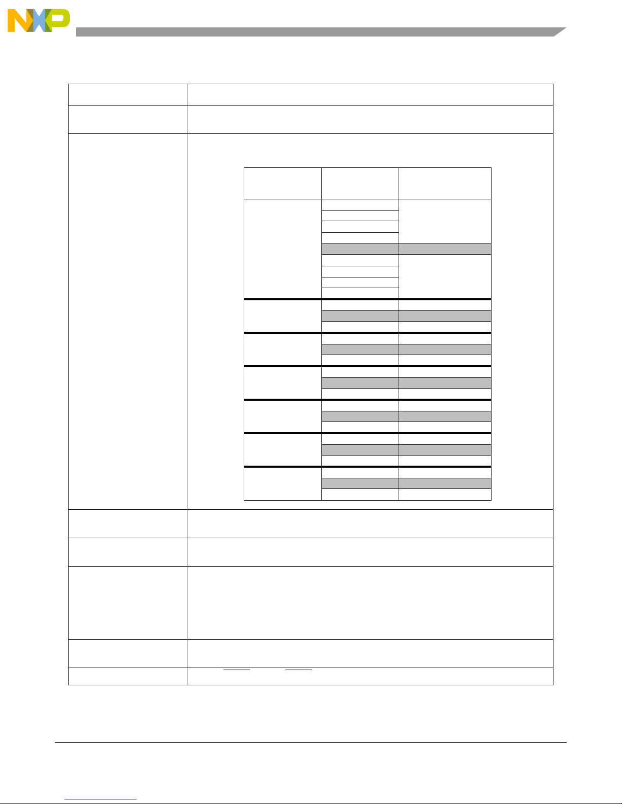
Interrupt
Level
ICR[IL]
Priority
ICR[IP]
Supported Interrupt
Sources
7
7
#8–63
6
5
4
— (Mid-point) #7 (IRQ7)
3
#8–63
2
1
0
6
7–4 #8–63
— (Mid-point) #6 (IRQ6)
3–0 #8–63
5
7–4 #8–63
— (Mid-point) #5 (IRQ5)
3–0 #8–63
4
7–4 #8–63
— (Mid-point) #4 (IRQ4)
3–0 #8–63
3
7–4 #8–63
— (Mid-point) #3 (IRQ3)
3–0 #8–63
2
7–4 #8–63
— (Mid-point) #2 (IRQ2)
3–0 #8–63
1
7–4 #8–63
— (Mid-point) #1 (IRQ1)
3–0 #8–63
Table 1. MCF5235RM Rev 2 Errata (continued)
Location Description
Table 12-10/Page 12-22 In PAR_TSIZ1 field change CIM to CCM.
In PAR_TSIZ0 field change CIM to CCM.
Table 13-1/Page 13-3 Replace table with the one below to better illustrate the interrupt priority and level
assignments.
Table 13-2/Page 13-5 In footnote, remove mention of the SWIACK register, as it is not supported in the global
Table 13-3/Page 13-6 Added global IACK addresses for the L1IACK–L7IA CK registers in the IPSBAR offset
Section 13.2.1.7/Page 13-18 Change last paragraph to: “In addition to the IACK registers within each interrupt controller,
Section 14.4/Page 14-13 Remove last sentence in this section starting with “BCRn decrements...” since SAA bit is
Section 14.4.4.1/Page 14-16 Change DREQ
Freescale Semiconductor 3
IACK space.
column, 0xFE4–0xFFC.
there are global LnIACK registers. A read from one of the global LnIACK registers returns
the vector for the highest priority unmasked interrupt within a level for all interrupt
controllers. There is no global SWIACK register. However, reading the SWIACK register
from each interrupt controller return s the vector number of the highest priority unmasked
request within that controller.”
not supported.
[32:0] to DREQ[3:0].
MCF5235 Reference Manual Errata, Rev. 2.2
Page 4

Errata for Revision 2
Table 1. MCF5235RM Rev 2 Errata (continued)
Location Description
Figure 14-9/Page 14-17 Change CLKIN to CLKOUT
Add overbars to TS, CS, and TA.
Section 14.4.4.1/Page 14-17 Remov e all text and figures in this section starting with “Since bus timings...”
Figure 15-3/Page 15-4 Figure incorrectly shows that EPDDR is 16-bits wide. Change to an 8-bit register with each
EPDDn bit a one-bit field from bits 7–1 to match Table 15-4.
Figure 16-2/Page 16-5 Re-labeled the WS states in the timing diagram. The first should be IWS to indicate that the
length of this wait state is determined by CSCR[IWS]. The rest of the wait states should be
IWS/SWWS to indicate that either CSCR[IWS] or CSCR[SWWS] determine the length of
the wait state depending on the value of CSCR[AA].
Figure 16-3/Page 16-5 Re-labeled the WS states in the timing diagram. The first should be IWS to indicate that the
length of this wait state is determined by CSCR[IWS]. The rest of the wait states should be
IWS/SRWS to indicate that either CSCR[IWS] or CSCR[SRWS] determine the length of the
wait state depending on the value of CSCR[AA].
Change Write labels on the data signals to Read.
Table 18-5/Page 18-8 Add the following note to the DACRn[CBM] field description:
Note: It is important to set CBM according to the location of the command bit.
Table 19-1/Page 19-5 Correct MIB block counters end address to IPSBAR + 0x12FF.
Table 19-3/Page 19-8 Add RMON_R_DROP with an IPSBAR Offset of 0x1280 and a description of ‘Count of
frames not counted correctly’.
Section 19.3.6/Page 19-38 Add the following subsection entitled “Duplicate Frame Transmission”:
The FEC fetches transmit buffer descriptors (TxBDs) and the corresponding transmit data
continuously until the transmit FIFO is full. It does not determine whether the TxBD to be
fetched is already being processed internally (as a result of a wrap). As the FEC nears the
end of the transmission of one frame, it begins to DMA the data for the next frame. In order
to remain one BD ahead of the DMA, it also fetches the TxBD for the next frame. It is
possible that the FEC will fetch from memory a BD that has already been processed but not
yet written back (that is, it is read a second time with the R bit still set). In this case, the data
is fetched and transmitted again.
Using at least three TxBDs fixes this problem for large frames , but not for small frames. To
ensure correct operation for either large or small frames, one of the following must be true:
• The FEC software driver ensures that there is always at least one TxBD with the ready
bit cleared.
• Every frame uses more than one TxBD and every TxBD but the last is written back
immediately after the data is fetched.
• The FEC software driver ensures a minimum frame size, n. The minimum number of
TxBDs is then (Tx FIFO Size ÷ (n + 4)) rounded up to the nearest integer (though the
result cannot be less than three). The default Tx FIFO size is 192 bytes; this size is
programmable.
Figure 30-8/Page 30-7 Move SKMR[CTRM,DKP] bit fieldsfrom 11–7 to 12–8.
Table 30-2/Page 30-8 Correct bit locations for CTRM and DKP fields:
31–13 Reserved
12–9 CTRM
8 DKP
7–5 Reserved
Table 32-13/Page 32-13 Add the following note to the PBR[Address] field description:
Note: PBR[0] should always be loaded with a 0.
MCF5235 Reference Manual Errata, Rev. 2.2
Freescale Semiconductor4
Page 5

Errata for Revision 1.1
2 Errata for Revision 1.1
Table 2. MCF5235RM Rev 1.1 Errata
Location Description
Throughout Remove overbar from DACKn signal s, as they are not asserted low.
Table 2- 1/Page 2-6 ERXER dire cti o n sho u l d be input, ETXEN direction should be output.
Table 2-1/Page 2-8 For 196BGA package, change pin F10 from OVDD to VSS.
Table 2-5/Page 2-10 Byte Strobes function column should say: “BS0 controls access to the least significant byte
lane of data, and BS3 controls access to the most significant byte lane of data.” and also
“Note that most SDRAMs associate DQM3 with the MSB, in which case BS
connected to the SDRAM's DQM3 input.”
Table 2-9/Page 2-12 ERXER direction should be input.
Table 2-14/Page 2-16 Add entry in table for PSTCLK output signal. “PSTCLK indicates when the development
system should sample PST and DDATA values.”
Figure 3-6/Page 3-17
Table 3-10/Page 3-18
Figure 3-7/Page 3-18 The reset value of D1[DCSIZ] is 0x0 and the reset value of D1[RAM1SIZ] is 0x8. Table 3-11
The reset value of D0[DEBUG] is 0x0. The debug revision of the MCF5235 is Re v. A. Tab le
3-10 is incorrect as well.
is correct
3 should be
Section 7.1.3.5/Page 7-6 The PLL cannot be stopped when the device enters stop mode. Remove paragraphs 3-6
and add in their place “During stop mode, the PLL continues to run. The external
CLKOUT signal may be enabled or disabled when the device enters stop mode,
depending on the LPCR[STPMD] bit settings. The external CLKOUT output pin may be
disabled to lower power consumption via the SYNCR[DISCLK] bit. The external
CLKOUT pin function is enabled by default at reset.”
Table 7-3/Page 7-7 Footnote should read: “In 1:1 mode for the MCF5235, f
Table 7-5/Page 7-9 The first equation in footnote #1 in the MFD bit description field is incorrect. It should be:
“f
sys=fref
× 2(MFD + 2)/2
RFD
” instead of f
sys/2
.
sys
= 2 × f
ref_1:1
”
T able 7-5/Page 7-9 The second equation in footnote #1 in the MFD bit description field is incorrect. It should be:
“f
× 2(MFD + 2) ≤ 150MHz” instead 75MHz
ref
Section 7.4.3/Page 7-15 First paragraph, the default core frequency is one and a half times the ref erence frequency
after reset instead of two times the reference frequency. An MFD = 0b001 is 6x not 2x.
Table 7-11/Page 7-30 Delete 4th and 5th rows on this page, as the PLL cannot be disabled in stop mode.
Table 8-4/Page 8-4 The description of bits 2-0 is mi ssing from the LPCR Field Description table. These should
be included with the following description: “Reserved, should be cleared.”
Section 8.3.2.3/Page 8-6 Corrected second paragraph since the core watchdog cannot reset the device. Second
paragraph should read “When enabled, the core watchdog can bring the device out of
low-power mode via a core watchdog interrupt. This system setup must meet the
conditions specified in Section 8.3.1, “Low-Power Modes” f or the core watchdog interrupt
to bring the part out of low-power mode.”
Section 8.3.2.16/Page 8-10 The PLL cannot be stopped when the device enters stop mode. Remove paragraphs 2-5
and add in their place “During stop mode, the PLL continues to run. The external
CLKOUT signal may be enabled or disabled when the device enters stop mode,
depending on the LPCR[STPMD] bit settings.”
Freescale Semiconductor 5
MCF5235 Reference Manual Errata, Rev. 2.2
Page 6

Errata for Revision 1.1
Table 2. MCF5235RM Rev 1.1 Errata (continued)
Location Description
Section 8.3.2.20/Page 8-10 The FlexCAN module does not support self-wake or auto-power save modes. Therefore,
change the following:
• Remove second paragraph.
• Change second sentence in first paragraph to “The module has 18 interrupt sources (16
sources due to message buffers and 2 sources due to bus-off and error).”
• Change STOP bit to MDIS bit throughout.
• Change MCR to CANMCR throughout.
• Remove third bullet under “Exiting stop mode is done in one of the following ways”
• Remove second sentence in second bullet under “Recommendations for...”
• Remove bullets 4-8 under “Recommendations for...”
• Remove last 3 paragraphs and last bullet list.
Table 9-1/Page 9-2 Reset config override signals should be D[25:24, 21:19, 16] instead of D[26:24, 21, 19:16].
Section 9.2.3/Page 9-3 Section title should be “D[25:24, 21:19, 16]...” instead of “D[26:24, 21, 19:16]...”
Figure 9-3/Page 9-5 Unreserved RCON register bits should be read only.
Table 9-7/Page 9-8 Reset config override signals should be D[25:24, 21:19, 16] instead of D[26:24, 21, 19:16].
Table 9-8/Page 9-8 Chip mode heading should be D16 only, since D26 & D17 have no affect on the selected
chip mode. Master mode (default) is selected by asserting D16. Deasserting D16 during
assertion at reset places the device in a reserved mode.
RCON
Table 9-8/Page 9-8 Remove “RCON[2]=0” in boot device default configuration field.
Table 9-8/Page 9-8 Default output pad drive strength should be partial instead of full.
Table 9-8/Page 9-9 Remove “RCON[7:6]=10” from clock mode default configuration field. Footnote added:
“There is no default configuration for clock mode selection. The actual values for the
CLKMOD pins must always be driven during reset. Once out of reset, the CLKMOD pins
have no effect on the clock mode selection.”
Table 9-8/Page 9-9 “Chip select configuration“ entry for setting D[25:24]=11, should read “PADDR[7:5] =
[6:4]” instead of “PADDR[7:6] = CS[6:4]”
CS
Table 9-8/Page 9-9 Footnote #2: Changed which pins do not affect reset configuration: “The D[31:26, 23:22,
18:17, 15:0] pins do not affect reset configuration.”
Section 9.4.2/Page 9-9 The MODE field is in the RCON register instead of the CCR.
Table 9-9/Page 9-9 Remove MODE[2] and MODE[1] columns since the MODE field is only one bit wide and
also D26 and D17 have no affect on chip configuration mode selection.
Table 12-1/Page 12-7 ERXER direction should be input, ETXEN direction should be output.
Table 12-1/Page 12-9 For 196BGA package, change pin F10 from OVDD to VSS.
Table 12-10/Page 12-22 Change an erroneous TSIZ1 to TSIZ0 in the PAR_TSIZ0 entry.
Figure 14-9/Page 14-16 DACKn is only asserted for a single clock cycle. All other signals (TS, CS, TA, R/W
, and
A[23:0] are subsequently moved one cycle sooner.
Throughout Chapter 16 Replace instances of D[19:18] with D[20:19].
Section 16.2.1/Page 16-1 An overbar should be placed over the CS[7:0] in the section heading.
The last sentence should read: “Port size for CS0 is configured by the logic levels of
D[20:19] when RSTOUT
negates and RCON is asserted.”
Table 16-6/Page 16-9 In the CSMRn[BAM] bit description, the first example BAM bit setting is incorrect. Change
from 0x0008 to 0x0001.
MCF5235 Reference Manual Errata, Rev. 2.2
Freescale Semiconductor6
Page 7

Errata for Revision 1.1
Table 2. MCF5235RM Rev 1.1 Errata (continued)
Location Description
Section 18.3.4.1/Page 18-10 Add Note “Because the device has 24 external address lines, the maximum SDRAM
address size is 128 Mbits.”
Throughout Chapter 19 The maximum buffer size of the FEC is 2032 bytes . Replace all instances of 2047 with 2032.
R_BUF_SIZE is at bit position 10:4 in the EMRBR register. Therefore the maximum
setting is $7F0 which equals 2032.
Figure 19-24/Page 19-28 Change EMRBR register address to “IPSBAR + 0x1188” instead of “IPSBAR +0x11B8”.
Section 21.3.2.6/Page 21-16 Remove reference to WAKINT in second paragraph
Figure 22-1/Page 22-2 Change value in divide by box to 4096 instead of 8192.
Table 24-3/Page 24-6 The MODE16 bit field description should read: “Selects the increment mode for the timer.
MODE16 = 1 is intended to exercise the upper bits of the 32-bit timer in diagnostic software
without requiring the timer to count through its entire dynamic range. When set, the
counter’s upper 16 bits mirror its lower 16 bits. All 32 bits of the counter are still compared
to the reference value.”
Figure 26-17/Page 26-18 Remove 16-bit divider blocks from both timer inputs, as it is not available when using an
external clock source.
Section 26.4.1.2.2/Page
26-19
Change equation to: Baudrate = f
using an external clock source.
Section 28.4.1/Page 28-15 Swap steps 4 & 5 and change “...(without padding) in bits” to “...(without padding) in bytes”.
Section 28.4.2.1/Page 28-16 Swap steps 4 & 5.
/(16 or 1), since the 16-bit divider is not available when
extc
Section 28.4.2.2/Page 28-16 Swap steps 4 & 5.
Section 28.4.2.3/Page 28-17 Swap steps 8 & 9.
Section 28.4.3/Page 28-18 Swap steps 8 & 9.
Section 28.4.4/Page 28-18 Swap steps 6 & 7.
Section 28.4.5/Page 28-18 Swap steps 7 & 8.
Figure 30-8/Page 30-7 Change SKMR[CTRM] bit field to straddle bits 11–8.
Table 30-2/Page 30-8 Change the first 4 SKMR bit fields bit numbers to 31–12, 11–8, 7, & 6–5.
Section 30.3.1/Page30-19 Remove last sentence of section, as this refers to internal logic only.
Section 30.4.1/Page 30-20 Swap steps 9 & 10.
Section 30.4.2/Page 30-20 Swap steps 9 & 10.
Swap steps 23 & 24.
Figure 30-7/Page 30-15 Replace entries with “Bytes 5-7 + P arity” with “Bytes 5-8” to reduce confusion. The parity is
included in the last bit of each byte, not the 8th byte.
Throughout Chapter 32 Replace CLKOUT with PSTCLK throughout.
Chapter 32 Add the following note to the beginning of the eTPU debug section: “eTPU debug
functionality is not available when the ColdFire processor is halted (STOP, DOZE, or
WAIT modes).”
Freescale Semiconductor 7
MCF5235 Reference Manual Errata, Rev. 2.2
Page 8

Revision History
3 Revision History
Table 3 provides a revision history for this document.
Table 3. Revision History Table
Rev. Number Substantive Changes Date of Release
1.0 • Initial release. 10/2004
1.1 • Added DACKn overbar errata.
• Added Byte Strobe errata.
• Added LPCR[2:0] descriptions.
• Added various RCON errata.
• Added chip mode errata.
• Added DACKn asserted for a single cycle errata.
1.2 • Added D0 & D1 reset value errata.
• Added FEC max buffer size errata.
• Added eTPU debug errata.
• Added FEC EMRBR address errata.
1.3 • Corrected previous errata with Table 9-8, Footnote #2.
• Added WAKEINT errata in Chapter 21.
• Added PAR_TSIZ0 errata.
• Added D[19:18]->D[20:19] errata.
• Added PSTCLK errata in Chapter 32.
1.4 • Added pin F10 errata in Chapter 2 and 12.
• Added ERXER and ETXER direction errata in Chapter 2 and 12.
• Added default output pad drive strength errata.
• Added Table 7-3 footnote errata.
• Added SKHA parity errata
• Added UART external clock source, 16-bit divider errata.
1.5 • Added FlexCAN errata in power management chapter. 12/2005
1.6 • Added PSTCLK errata in Chapter 2.
• Added multiple errata regarding the PLL unable to be stopped during stop
mode.
• Added MFD bit field errata.
• Added core watchdog reset errata.
• Added reset config override signal description errata in Chapter 9.
• Added chip select configuration entry errata.
• Added chip select signal description errata in Chapter 16.
• Added CSMRn[BAM] example errata.
• Added SDRAM address line note errata.
• Added DMA Timer MODE16 bit errata.
• Added MDHA & SKHA application examples errata.
• Added the SKMR[CTRM] bit field errata.
1.7 • Added watchdog timer divide-by value errata. 07/2006
11/2004
03/2005
07/2005
08/2005
03/2006
MCF5235 Reference Manual Errata, Rev. 2.2
Freescale Semiconductor8
Page 9

Revision History
Table 3. Revision History Table (continued)
Rev. Number Substantive Changes Date of Release
The below errata were added for MCF5235RM Revision 2
2 • Added QSPI_CS/SD_CKE pin location errata. 08/2006
2.1 • Added RMON_R_DROP counter errata. 11/2006
2.2 • Added various core, EMAC, cache, SRAM and debu g chapter errata.
• Added CLKIN to CLKOUT errata.
• Added FEC MIB counter memory map errata.
• Added “Duplicate Frame Transmission” section to FEC chapter.
• Added DACRn[CBM] field description note.
• Added secondary wait state timing diagram errata.
• Added SKMR[CTRM,DKP] errata.
• Added CIM/CCM errata.
• Added EPDDR figure errata.
• Added DMA figure overbars errata.
• Added DMA external request and acknowledge operation section errata.
• Added DMA SAA bit errata.
• Added IPSBAR note in SCM chapter.
• Added global IACK space errata.
05/2007
Freescale Semiconductor 9
MCF5235 Reference Manual Errata, Rev. 2.2
Page 10

How to Reach Us:
Home Page:
www.freescale.com
E-mail:
support@freescale.com
USA/Europe or Locations Not Listed:
Freescale Semiconductor
Technical Information Center, CH370
1300 N. Alma School Road
Chandler, Arizona 85224
+1-800-521-6274 or +1-480-768-2130
support@freescale.com
Europe, Middle East, and Africa:
Freescale Halbleiter Deutschland GmbH
Technical Information Center
Schatzbogen 7
81829 Muenchen, Germany
+44 1296 380 456 (English)
+46 8 52200080 (English)
+49 89 92103 559 (German)
+33 1 69 35 48 48 (French)
support@freescale.com
Japan:
Freescale Semiconductor Japan Ltd.
Headquarters
ARCO Tower 15F
1-8-1, Shimo-Meguro, Meguro-ku,
Tokyo 153-0064, Japan
0120 191014 or +81 3 5437 9125
support.japan@freescale.com
Asia/Pacific:
Freescale Semiconductor Hong Kong Ltd.
Technical Information Center
2 Dai King Street
Tai Po Industrial Estate
Tai Po, N.T., Hong Kong
+800 2666 8080
support.asia@freescale.com
For Literature Requests Only:
Freescale Semiconductor Literature Distribution Center
P.O. Box 5405
Denver, Colorado 80217
1-800-441-2447 or 303-675-2140
Fax: 303-675-2150
LDCForFreescaleSemiconductor@hibbertgroup.com
Information in this document is provided solely to enable system and
software implementers to use F reescal e Semiconductor pr oducts. There are
no express or implied copyright licenses granted hereunder to design or
fabricate any integrated circuits or integrated circuits based on the
information in this document.
Freescale Semiconducto r reserves the right to make ch anges without further
notice to any products herein. F reescal e Semiconducto r make s no warra nty,
representation or guarantee regarding the suitability of its products for any
particular purpose, nor does Freescale Semiconductor assume any liability
arising out of the application or use of any produc t or circuit, and spe cifical ly
disclaims any and all liability, including without limitation consequential or
incidental damages. “Typical” parameters that may be pro vided in F r eescale
Semiconductor data sheets and/or spec ifications can and do v ary in differ ent
applications and actual performance may vary over time. All operating
parameters, including “Typicals”, must be validated for each customer
application by customer’s technical experts. Freescale Semiconductor does
not convey any license under its patent rights nor the rights of others.
Freescale Semicondu ctor products are not desi gned, intended, or aut horized
for use as components in systems intended for surgical implant into the body,
or other applications intended to support or sustain life, or for any other
application in which the failure of the Freescale Semiconductor product could
create a situation where personal injury or death may occur. Should Buyer
purchase or use Freescal e Semiconductor prod ucts for an y such unintended
or unauthorized application, Buyer shall in demnify and hold Freescale
Semiconductor and its officers, employees, subsidiaries, affiliates, and
distributors harmless against all claims, costs, damages, and expenses, and
reasonable attorney fees arising out of, directly or indirectly, any claim of
personal injury or death associated with such unintended or unauthorized
use, even if such claim alleges that Freescale Semiconductor was negligent
regarding the design or manufacture of the part.
Freescale™ and the Freescale logo are trademarks of Freescale
Semiconductor, Inc. All other product or service names are the property
of their respective owners.© Freescale Semiconductor, Inc. 2007. All rights
reserved.
MCF5235RMAD
Rev. 2.2
05/2007
 Loading...