

Page 1

MC9S12XS256
Reference Manual
Covers MC9S12XS Family
MC9S12XS256
MC9S12XS128
MC9S12XS64
HCS12
Microcontrollers
MC9S12XS256RMV1
Rev. 1.13
08/2012
freescale.com
Page 2

To provide the most up-to-date information, the document revision on the World Wide Web is the most
current. A printed copy may be an earlier revision. To verify you have the latest information available,
refer to freescale.com.
This document contains information for the complete S12XS Family and thus includes a set of separate
flash (FTMR) module sections to cover the whole family. A full list of family members and options is
included in the appendices.
This document contains information forall constituent modules, with the exception of the CPU. For CPU
information please refer to CPU12XV1 in the CPU12/CPU12X Reference Manual.
Revision History
Date
November,
2010
Jul, 2011 1.12
Aug, 2012 1.13
Revision
Level
1.11
Description
Updated Chapter 3 Memory Mapping Control (S12XMMCV4)
Updated Chapter 11 Freescale’s Scalable Controller Area Network
(S12MSCANV3)
Updated Chapter 14 Serial Communication Interface (S12SCIV5)
Updated footnotes on table 1-2
Updated note in Appendix F Ordering Information
Corrected API accuracy in feature list
Corrected name of pin #27 in 80QFP pinout (PE5->PE4)
Updated Chapter 2 Port Integration Module (S12XSPIMV1)
Updated Chapter 11 Freescale’s Scalable Controller Area Network
(S12MSCANV3)
Updated Chapter 4 Interrupt (S12XINTV2)
Updated Chapter 8 S12XE Clocks and Reset Generator (S12XECRGV1)
Updated V
Minor editorial corrections in:
Chapter 2 Port Integration Module (S12XSPIMV1)
Chapter 5 Background Debug Module (S12XBDMV2)
Chapter 6 S12X Debug (S12XDBGV3) Module
max. voltage in Appendix A Electrical Characteristics
DDF
Page 3

Chapter 1 Device Overview S12XS Family . . . . . . . . . . . . . . . . . . . . . . . . . . . . . . . . .19
Chapter 2 Port Integration Module (S12XSPIMV1) . . . . . . . . . . . . . . . . . . . . . . . . . . .59
Chapter 3 Memory Mapping Control (S12XMMCV4) . . . . . . . . . . . . . . . . . . . . . . . .127
Chapter 4 Interrupt (S12XINTV2) . . . . . . . . . . . . . . . . . . . . . . . . . . . . . . . . . . . . . . . .151
Chapter 5 Background Debug Module (S12XBDMV2) . . . . . . . . . . . . . . . . . . . . . . .169
Chapter 6 S12X Debug (S12XDBGV3) Module . . . . . . . . . . . . . . . . . . . . . . . . . . . . .195
Chapter 7 Security (S12XS9SECV2). . . . . . . . . . . . . . . . . . . . . . . . . . . . . . . . . . . . . .231
Chapter 8 S12XE Clocks and Reset Generator (S12XECRGV1) . . . . . . . . . . . . . . .237
Chapter 9 Pierce Oscillator (S12XOSCLCPV2) . . . . . . . . . . . . . . . . . . . . . . . . . . . .267
Chapter 10 Analog-to-Digital Converter (ADC12B16CV1) . . . . . . . . . . . . . . . . . . . . .271
Chapter 11 Freescale’s Scalable Controller Area Network (S12MSCANV3) . . . . . .295
Chapter 12 Periodic Interrupt Timer (S12PIT24B4CV1) . . . . . . . . . . . . . . . . . . . . . . .349
Chapter 13 Pulse-Width Modulator (S12PWM8B8CV1) . . . . . . . . . . . . . . . . . . . . . . .365
Chapter 14 Serial Communication Interface (S12SCIV5). . . . . . . . . . . . . . . . . . . . . .397
Chapter 15 Serial Peripheral Interface (S12SPIV5). . . . . . . . . . . . . . . . . . . . . . . . . . .435
Chapter 16 Timer Module (TIM16B8CV2). . . . . . . . . . . . . . . . . . . . . . . . . . . . . . . . . . .461
Chapter 17 Voltage Regulator (S12VREGL3V3V1) . . . . . . . . . . . . . . . . . . . . . . . . . . .489
Chapter 18 256 KByte Flash Module (S12XFTMR256K1V1). . . . . . . . . . . . . . . . . . . .507
Chapter 19 128 KByte Flash Module (S12XFTMR128K1V1). . . . . . . . . . . . . . . . . . . .557
Chapter 20 64 KByte Flash Module (S12XFTMR64K1V1). . . . . . . . . . . . . . . . . . . . . .607
Appendix A Electrical Characteristics . . . . . . . . . . . . . . . . . . . . . . . . . . . . . . . . . . . . .657
Appendix B Package Information . . . . . . . . . . . . . . . . . . . . . . . . . . . . . . . . . . . . . . . . .698
Appendix C PCB Layout Guidelines . . . . . . . . . . . . . . . . . . . . . . . . . . . . . . . . . . . . . . .708
Appendix D Derivative Differences . . . . . . . . . . . . . . . . . . . . . . . . . . . . . . . . . . . . . . . .712
Appendix E Detailed Register Address Map . . . . . . . . . . . . . . . . . . . . . . . . . . . . . . . .713
Appendix F Ordering Information . . . . . . . . . . . . . . . . . . . . . . . . . . . . . . . . . . . . . . . . .735
S12XS Family Reference Manual, Rev. 1.13
Freescale Semiconductor 3
Page 4

S12XS Family Reference Manual, Rev. 1.13
4 Freescale Semiconductor
Page 5

Chapter 1
Device Overview S12XS Family
1.1 Introduction . . . . . . . . . . . . . . . . . . . . . . . . . . . . . . . . . . . . . . . . . . . . . . . . . . . . . . . . . . . . . . . . . . 19
1.1.1 Features . . . . . . . . . . . . . . . . . . . . . . . . . . . . . . . . . . . . . . . . . . . . . . . . . . . . . . . . . . . . . . 19
1.1.2 Modes of Operation . . . . . . . . . . . . . . . . . . . . . . . . . . . . . . . . . . . . . . . . . . . . . . . . . . . . .23
1.1.3 Block Diagram . . . . . . . . . . . . . . . . . . . . . . . . . . . . . . . . . . . . . . . . . . . . . . . . . . . . . . . . . 24
1.1.4 Device Memory Map . . . . . . . . . . . . . . . . . . . . . . . . . . . . . . . . . . . . . . . . . . . . . . . . . . . . 25
1.1.5 Address Mapping . . . . . . . . . . . . . . . . . . . . . . . . . . . . . . . . . . . . . . . . . . . . . . . . . . . . . . .26
1.1.6 Detailed Register Map . . . . . . . . . . . . . . . . . . . . . . . . . . . . . . . . . . . . . . . . . . . . . . . . . . . 28
1.1.7 Part ID Assignments . . . . . . . . . . . . . . . . . . . . . . . . . . . . . . . . . . . . . . . . . . . . . . . . . . . .28
1.2 Signal Description . . . . . . . . . . . . . . . . . . . . . . . . . . . . . . . . . . . . . . . . . . . . . . . . . . . . . . . . . . . . . 29
1.2.1 Device Pinout . . . . . . . . . . . . . . . . . . . . . . . . . . . . . . . . . . . . . . . . . . . . . . . . . . . . . . . . . . 29
1.2.2 Pin Assignment Overview . . . . . . . . . . . . . . . . . . . . . . . . . . . . . . . . . . . . . . . . . . . . . . . . 33
1.2.3 Detailed Signal Descriptions . . . . . . . . . . . . . . . . . . . . . . . . . . . . . . . . . . . . . . . . . . . . . . 41
1.2.4 Power Supply Pins . . . . . . . . . . . . . . . . . . . . . . . . . . . . . . . . . . . . . . . . . . . . . . . . . . . . . .45
1.3 System Clock Description . . . . . . . . . . . . . . . . . . . . . . . . . . . . . . . . . . . . . . . . . . . . . . . . . . . . . . . 48
1.4 Modes of Operation . . . . . . . . . . . . . . . . . . . . . . . . . . . . . . . . . . . . . . . . . . . . . . . . . . . . . . . . . . . . 49
1.4.1 Chip Configuration Summary . . . . . . . . . . . . . . . . . . . . . . . . . . . . . . . . . . . . . . . . . . . . . 49
1.4.2 Power Modes . . . . . . . . . . . . . . . . . . . . . . . . . . . . . . . . . . . . . . . . . . . . . . . . . . . . . . . . . . 50
1.4.3 Freeze Mode . . . . . . . . . . . . . . . . . . . . . . . . . . . . . . . . . . . . . . . . . . . . . . . . . . . . . . . . . . . 51
1.5 Security . . . . . . . . . . . . . . . . . . . . . . . . . . . . . . . . . . . . . . . . . . . . . . . . . . . . . . . . . . . . . . . . . . . . . . 51
1.6 Resets and Interrupts . . . . . . . . . . . . . . . . . . . . . . . . . . . . . . . . . . . . . . . . . . . . . . . . . . . . . . . . . . . 51
1.6.1 Resets . . . . . . . . . . . . . . . . . . . . . . . . . . . . . . . . . . . . . . . . . . . . . . . . . . . . . . . . . . . . . . . . 51
1.6.2 Vectors . . . . . . . . . . . . . . . . . . . . . . . . . . . . . . . . . . . . . . . . . . . . . . . . . . . . . . . . . . . . . . . 51
1.6.3 Effects of Reset . . . . . . . . . . . . . . . . . . . . . . . . . . . . . . . . . . . . . . . . . . . . . . . . . . . . . . . . 53
1.7 ATD0 Configuration . . . . . . . . . . . . . . . . . . . . . . . . . . . . . . . . . . . . . . . . . . . . . . . . . . . . . . . . . . . . 55
1.7.1 External Trigger Input Connection . . . . . . . . . . . . . . . . . . . . . . . . . . . . . . . . . . . . . . . . . 55
1.7.2 ATD0 Channel[17] Connection . . . . . . . . . . . . . . . . . . . . . . . . . . . . . . . . . . . . . . . . . . . . 55
1.8 VREG Configuration . . . . . . . . . . . . . . . . . . . . . . . . . . . . . . . . . . . . . . . . . . . . . . . . . . . . . . . . . . . 55
1.8.1 Temperature Sensor Configuration . . . . . . . . . . . . . . . . . . . . . . . . . . . . . . . . . . . . . . . . . 55
1.9 BDM Clock Configuration . . . . . . . . . . . . . . . . . . . . . . . . . . . . . . . . . . . . . . . . . . . . . . . . . . . . . . . 56
1.10 Oscillator Configuration . . . . . . . . . . . . . . . . . . . . . . . . . . . . . . . . . . . . . . . . . . . . . . . . . . . . . . . . . 56
Chapter 2
Port Integration Module (S12XSPIMV1)
2.1 Introduction . . . . . . . . . . . . . . . . . . . . . . . . . . . . . . . . . . . . . . . . . . . . . . . . . . . . . . . . . . . . . . . . . . 59
2.1.1 Overview . . . . . . . . . . . . . . . . . . . . . . . . . . . . . . . . . . . . . . . . . . . . . . . . . . . . . . . . . . . . . 59
2.1.2 Features . . . . . . . . . . . . . . . . . . . . . . . . . . . . . . . . . . . . . . . . . . . . . . . . . . . . . . . . . . . . . . 60
2.2 External Signal Description . . . . . . . . . . . . . . . . . . . . . . . . . . . . . . . . . . . . . . . . . . . . . . . . . . . . . . 60
2.3 Memory Map and Register Definition . . . . . . . . . . . . . . . . . . . . . . . . . . . . . . . . . . . . . . . . . . . . . .64
S12XS Family Reference Manual, Rev. 1.13
Freescale Semiconductor 5
Page 6

2.3.1 Memory Map . . . . . . . . . . . . . . . . . . . . . . . . . . . . . . . . . . . . . . . . . . . . . . . . . . . . . . . . . . 65
2.3.2 Register Descriptions . . . . . . . . . . . . . . . . . . . . . . . . . . . . . . . . . . . . . . . . . . . . . . . . . . . .73
2.3.3 Port A Data Register (PORTA) . . . . . . . . . . . . . . . . . . . . . . . . . . . . . . . . . . . . . . . . . . . . 75
2.3.4 Port B Data Register (PORTB) . . . . . . . . . . . . . . . . . . . . . . . . . . . . . . . . . . . . . . . . . . . . 75
2.3.5 Port A Data Direction Register (DDRA) . . . . . . . . . . . . . . . . . . . . . . . . . . . . . . . . . . . . . 76
2.3.6 Port B Data Direction Register (DDRB) . . . . . . . . . . . . . . . . . . . . . . . . . . . . . . . . . . . . . 76
2.3.7 PIM Reserved Registers . . . . . . . . . . . . . . . . . . . . . . . . . . . . . . . . . . . . . . . . . . . . . . . . . . 77
2.3.8 Port E Data Register (PORTE) . . . . . . . . . . . . . . . . . . . . . . . . . . . . . . . . . . . . . . . . . . . . 77
2.3.9 Port E Data Direction Register (DDRE) . . . . . . . . . . . . . . . . . . . . . . . . . . . . . . . . . . . . . 78
2.3.10 Ports ABEK, BKGD pin Pull-up Control Register (PUCR) . . . . . . . . . . . . . . . . . . . . . . 79
2.3.11 Ports ABEK Reduced Drive Register (RDRIV) . . . . . . . . . . . . . . . . . . . . . . . . . . . . . . . 80
2.3.12 ECLK Control Register (ECLKCTL) . . . . . . . . . . . . . . . . . . . . . . . . . . . . . . . . . . . . . . . 81
2.3.13 PIM Reserved Register . . . . . . . . . . . . . . . . . . . . . . . . . . . . . . . . . . . . . . . . . . . . . . . . . . 82
2.3.14 IRQ Control Register (IRQCR) . . . . . . . . . . . . . . . . . . . . . . . . . . . . . . . . . . . . . . . . . . . . 83
2.3.15 PIM Reserved Register PIMTEST . . . . . . . . . . . . . . . . . . . . . . . . . . . . . . . . . . . . . . . . . . 83
2.3.16 Port K Data Register (PORTK) . . . . . . . . . . . . . . . . . . . . . . . . . . . . . . . . . . . . . . . . . . . . 84
2.3.17 Port K Data Direction Register (DDRK) . . . . . . . . . . . . . . . . . . . . . . . . . . . . . . . . . . . . . 84
2.3.18 Port T Data Register (PTT) . . . . . . . . . . . . . . . . . . . . . . . . . . . . . . . . . . . . . . . . . . . . . . . 85
2.3.19 Port T Input Register (PTIT) . . . . . . . . . . . . . . . . . . . . . . . . . . . . . . . . . . . . . . . . . . . . . . 86
2.3.20 Port T Data Direction Register (DDRT) . . . . . . . . . . . . . . . . . . . . . . . . . . . . . . . . . . . . . 87
2.3.21 Port T Reduced Drive Register (RDRT) . . . . . . . . . . . . . . . . . . . . . . . . . . . . . . . . . . . . . 87
2.3.22 Port T Pull Device Enable Register (PERT) . . . . . . . . . . . . . . . . . . . . . . . . . . . . . . . . . . 88
2.3.23 Port T Polarity Select Register (PPST) . . . . . . . . . . . . . . . . . . . . . . . . . . . . . . . . . . . . . . 88
2.3.24 PIM Reserved Register . . . . . . . . . . . . . . . . . . . . . . . . . . . . . . . . . . . . . . . . . . . . . . . . . . 89
2.3.25 Port T Routing Register (PTTRR) . . . . . . . . . . . . . . . . . . . . . . . . . . . . . . . . . . . . . . . . . . 89
2.3.26 Port S Data Register (PTS) . . . . . . . . . . . . . . . . . . . . . . . . . . . . . . . . . . . . . . . . . . . . . . . 91
2.3.27 Port S Input Register (PTIS) . . . . . . . . . . . . . . . . . . . . . . . . . . . . . . . . . . . . . . . . . . . . . . 92
2.3.28 Port S Data Direction Register (DDRS) . . . . . . . . . . . . . . . . . . . . . . . . . . . . . . . . . . . . . 93
2.3.29 Port S Reduced Drive Register (RDRS) . . . . . . . . . . . . . . . . . . . . . . . . . . . . . . . . . . . . . 94
2.3.30 Port S Pull Device Enable Register (PERS) . . . . . . . . . . . . . . . . . . . . . . . . . . . . . . . . . . 94
2.3.31 Port S Polarity Select Register (PPSS) . . . . . . . . . . . . . . . . . . . . . . . . . . . . . . . . . . . . . . 95
2.3.32 Port S Wired-Or Mode Register (WOMS) . . . . . . . . . . . . . . . . . . . . . . . . . . . . . . . . . . . . 95
2.3.33 PIM Reserved Register . . . . . . . . . . . . . . . . . . . . . . . . . . . . . . . . . . . . . . . . . . . . . . . . . . 96
2.3.34 Port M Data Register (PTM) . . . . . . . . . . . . . . . . . . . . . . . . . . . . . . . . . . . . . . . . . . . . . . 96
2.3.35 Port M Input Register (PTIM) . . . . . . . . . . . . . . . . . . . . . . . . . . . . . . . . . . . . . . . . . . . . . 98
2.3.36 Port M Data Direction Register (DDRM) . . . . . . . . . . . . . . . . . . . . . . . . . . . . . . . . . . . . 98
2.3.37 Port M Reduced Drive Register (RDRM) . . . . . . . . . . . . . . . . . . . . . . . . . . . . . . . . . . . . 99
2.3.38 Port M Pull Device Enable Register (PERM) . . . . . . . . . . . . . . . . . . . . . . . . . . . . . . . . 100
2.3.39 Port M Polarity Select Register (PPSM) . . . . . . . . . . . . . . . . . . . . . . . . . . . . . . . . . . . . 100
2.3.40 Port M Wired-Or Mode Register (WOMM) . . . . . . . . . . . . . . . . . . . . . . . . . . . . . . . . . 101
2.3.41 Module Routing Register (MODRR) . . . . . . . . . . . . . . . . . . . . . . . . . . . . . . . . . . . . . . . 101
2.3.42 Port P Data Register (PTP) . . . . . . . . . . . . . . . . . . . . . . . . . . . . . . . . . . . . . . . . . . . . . . 102
2.3.43 Port P Input Register (PTIP) . . . . . . . . . . . . . . . . . . . . . . . . . . . . . . . . . . . . . . . . . . . . . 104
2.3.44 Port P Data Direction Register (DDRP) . . . . . . . . . . . . . . . . . . . . . . . . . . . . . . . . . . . . 105
2.3.45 Port P Reduced Drive Register (RDRP) . . . . . . . . . . . . . . . . . . . . . . . . . . . . . . . . . . . . 106
S12XS Family Reference Manual, Rev. 1.13
6 Freescale Semiconductor
Page 7

2.3.46 Port P Pull Device Enable Register (PERP) . . . . . . . . . . . . . . . . . . . . . . . . . . . . . . . . . 106
2.3.47 Port P Polarity Select Register (PPSP) . . . . . . . . . . . . . . . . . . . . . . . . . . . . . . . . . . . . . 107
2.3.48 Port P Interrupt Enable Register (PIEP) . . . . . . . . . . . . . . . . . . . . . . . . . . . . . . . . . . . . 107
2.3.49 Port P Interrupt Flag Register (PIFP) . . . . . . . . . . . . . . . . . . . . . . . . . . . . . . . . . . . . . . . 108
2.3.50 Port H Data Register (PTH) . . . . . . . . . . . . . . . . . . . . . . . . . . . . . . . . . . . . . . . . . . . . . . 108
2.3.51 Port H Input Register (PTIH) . . . . . . . . . . . . . . . . . . . . . . . . . . . . . . . . . . . . . . . . . . . . . 109
2.3.52 Port H Data Direction Register (DDRH) . . . . . . . . . . . . . . . . . . . . . . . . . . . . . . . . . . . . 109
2.3.53 Port H Reduced Drive Register (RDRH) . . . . . . . . . . . . . . . . . . . . . . . . . . . . . . . . . . . . 110
2.3.54 Port H Pull Device Enable Register (PERH) . . . . . . . . . . . . . . . . . . . . . . . . . . . . . . . . . 110
2.3.55 Port H Polarity Select Register (PPSH) . . . . . . . . . . . . . . . . . . . . . . . . . . . . . . . . . . . . . 111
2.3.56 Port H Interrupt Enable Register (PIEH) . . . . . . . . . . . . . . . . . . . . . . . . . . . . . . . . . . . . 111
2.3.57 Port H Interrupt Flag Register (PIFH) . . . . . . . . . . . . . . . . . . . . . . . . . . . . . . . . . . . . . . 112
2.3.58 Port J Data Register (PTJ) . . . . . . . . . . . . . . . . . . . . . . . . . . . . . . . . . . . . . . . . . . . . . . . 112
2.3.59 Port J Input Register (PTIJ) . . . . . . . . . . . . . . . . . . . . . . . . . . . . . . . . . . . . . . . . . . . . . . 113
2.3.60 Port J Data Direction Register (DDRJ) . . . . . . . . . . . . . . . . . . . . . . . . . . . . . . . . . . . . . 113
2.3.61 Port J Reduced Drive Register (RDRJ) . . . . . . . . . . . . . . . . . . . . . . . . . . . . . . . . . . . . . 114
2.3.62 Port J Pull Device Enable Register (PERJ) . . . . . . . . . . . . . . . . . . . . . . . . . . . . . . . . . . 114
2.3.63 Port J Polarity Select Register (PPSJ) . . . . . . . . . . . . . . . . . . . . . . . . . . . . . . . . . . . . . . 115
2.3.64 Port J Interrupt Enable Register (PIEJ) . . . . . . . . . . . . . . . . . . . . . . . . . . . . . . . . . . . . . 115
2.3.65 Port J Interrupt Flag Register (PIFJ) . . . . . . . . . . . . . . . . . . . . . . . . . . . . . . . . . . . . . . . 116
2.3.66 Port AD0 Data Register 0 (PT0AD0) . . . . . . . . . . . . . . . . . . . . . . . . . . . . . . . . . . . . . . 116
2.3.67 Port AD0 Data Register 1 (PT1AD0) . . . . . . . . . . . . . . . . . . . . . . . . . . . . . . . . . . . . . . 117
2.3.68 Port AD0 Data Direction Register 0 (DDR0AD0) . . . . . . . . . . . . . . . . . . . . . . . . . . . . 117
2.3.69 Port AD0 Data Direction Register 1 (DDR1AD0) . . . . . . . . . . . . . . . . . . . . . . . . . . . . 118
2.3.70 Port AD0 Reduced Drive Register 0 (RDR0AD0) . . . . . . . . . . . . . . . . . . . . . . . . . . . . 118
2.3.71 Port AD0 Reduced Drive Register 1 (RDR1AD0) . . . . . . . . . . . . . . . . . . . . . . . . . . . . 119
2.3.72 Port AD0 Pull Up Enable Register 0 (PER0AD0) . . . . . . . . . . . . . . . . . . . . . . . . . . . . . 119
2.3.73 Port AD0 Pull Up Enable Register 1 (PER1AD0) . . . . . . . . . . . . . . . . . . . . . . . . . . . . . 120
2.3.74 PIM Reserved Registers . . . . . . . . . . . . . . . . . . . . . . . . . . . . . . . . . . . . . . . . . . . . . . . . . 120
2.4 Functional Description . . . . . . . . . . . . . . . . . . . . . . . . . . . . . . . . . . . . . . . . . . . . . . . . . . . . . . . . . 120
2.4.1 General . . . . . . . . . . . . . . . . . . . . . . . . . . . . . . . . . . . . . . . . . . . . . . . . . . . . . . . . . . . . . . 120
2.4.2 Registers . . . . . . . . . . . . . . . . . . . . . . . . . . . . . . . . . . . . . . . . . . . . . . . . . . . . . . . . . . . . . 121
2.4.3 Pins and Ports . . . . . . . . . . . . . . . . . . . . . . . . . . . . . . . . . . . . . . . . . . . . . . . . . . . . . . . . . 123
2.4.4 Pin interrupts . . . . . . . . . . . . . . . . . . . . . . . . . . . . . . . . . . . . . . . . . . . . . . . . . . . . . . . . . 125
2.5 Initialization Information . . . . . . . . . . . . . . . . . . . . . . . . . . . . . . . . . . . . . . . . . . . . . . . . . . . . . . . 126
2.5.1 Port Data and Data Direction Register writes . . . . . . . . . . . . . . . . . . . . . . . . . . . . . . . . 126
Chapter 3
Memory Mapping Control (S12XMMCV4)
3.1 Introduction . . . . . . . . . . . . . . . . . . . . . . . . . . . . . . . . . . . . . . . . . . . . . . . . . . . . . . . . . . . . . . . . . 127
3.1.1 Terminology . . . . . . . . . . . . . . . . . . . . . . . . . . . . . . . . . . . . . . . . . . . . . . . . . . . . . . . . . . 128
3.1.2 Features . . . . . . . . . . . . . . . . . . . . . . . . . . . . . . . . . . . . . . . . . . . . . . . . . . . . . . . . . . . . . 128
3.1.3 S12X Memory Mapping . . . . . . . . . . . . . . . . . . . . . . . . . . . . . . . . . . . . . . . . . . . . . . . . 129
3.1.4 Modes of Operation . . . . . . . . . . . . . . . . . . . . . . . . . . . . . . . . . . . . . . . . . . . . . . . . . . . . 129
3.1.5 Block Diagram . . . . . . . . . . . . . . . . . . . . . . . . . . . . . . . . . . . . . . . . . . . . . . . . . . . . . . . . 129
S12XS Family Reference Manual, Rev. 1.13
Freescale Semiconductor 7
Page 8

3.2 External Signal Description . . . . . . . . . . . . . . . . . . . . . . . . . . . . . . . . . . . . . . . . . . . . . . . . . . . . . 130
3.3 Memory Map and Registers . . . . . . . . . . . . . . . . . . . . . . . . . . . . . . . . . . . . . . . . . . . . . . . . . . . . . 131
3.3.1 Module Memory Map . . . . . . . . . . . . . . . . . . . . . . . . . . . . . . . . . . . . . . . . . . . . . . . . . . 131
3.3.2 Register Descriptions . . . . . . . . . . . . . . . . . . . . . . . . . . . . . . . . . . . . . . . . . . . . . . . . . . . 131
3.4 Functional Description . . . . . . . . . . . . . . . . . . . . . . . . . . . . . . . . . . . . . . . . . . . . . . . . . . . . . . . . . 140
3.4.1 MCU Operating Mode . . . . . . . . . . . . . . . . . . . . . . . . . . . . . . . . . . . . . . . . . . . . . . . . . . 140
3.4.2 Memory Map Scheme . . . . . . . . . . . . . . . . . . . . . . . . . . . . . . . . . . . . . . . . . . . . . . . . . . 140
3.4.3 Chip Bus Control . . . . . . . . . . . . . . . . . . . . . . . . . . . . . . . . . . . . . . . . . . . . . . . . . . . . . . 147
3.5 Initialization/Application Information . . . . . . . . . . . . . . . . . . . . . . . . . . . . . . . . . . . . . . . . . . . . . 148
3.5.1 CALL and RTC Instructions . . . . . . . . . . . . . . . . . . . . . . . . . . . . . . . . . . . . . . . . . . . . . 148
Chapter 4
Interrupt (S12XINTV2)
4.1 Introduction . . . . . . . . . . . . . . . . . . . . . . . . . . . . . . . . . . . . . . . . . . . . . . . . . . . . . . . . . . . . . . . . . 151
4.1.1 Glossary . . . . . . . . . . . . . . . . . . . . . . . . . . . . . . . . . . . . . . . . . . . . . . . . . . . . . . . . . . . . . 152
4.1.2 Features . . . . . . . . . . . . . . . . . . . . . . . . . . . . . . . . . . . . . . . . . . . . . . . . . . . . . . . . . . . . . 152
4.1.3 Modes of Operation . . . . . . . . . . . . . . . . . . . . . . . . . . . . . . . . . . . . . . . . . . . . . . . . . . . . 153
4.1.4 Block Diagram . . . . . . . . . . . . . . . . . . . . . . . . . . . . . . . . . . . . . . . . . . . . . . . . . . . . . . . . 154
4.2 External Signal Description . . . . . . . . . . . . . . . . . . . . . . . . . . . . . . . . . . . . . . . . . . . . . . . . . . . . . 154
4.3 Memory Map and Register Definition . . . . . . . . . . . . . . . . . . . . . . . . . . . . . . . . . . . . . . . . . . . . . 155
4.3.1 Module Memory Map . . . . . . . . . . . . . . . . . . . . . . . . . . . . . . . . . . . . . . . . . . . . . . . . . . 155
4.3.2 Register Descriptions . . . . . . . . . . . . . . . . . . . . . . . . . . . . . . . . . . . . . . . . . . . . . . . . . . . 156
4.4 Functional Description . . . . . . . . . . . . . . . . . . . . . . . . . . . . . . . . . . . . . . . . . . . . . . . . . . . . . . . . . 161
4.4.1 S12X Exception Requests . . . . . . . . . . . . . . . . . . . . . . . . . . . . . . . . . . . . . . . . . . . . . . . 162
4.4.2 Interrupt Prioritization . . . . . . . . . . . . . . . . . . . . . . . . . . . . . . . . . . . . . . . . . . . . . . . . . . 162
4.4.3 XGATE Requests . . . . . . . . . . . . . . . . . . . . . . . . . . . . . . . . . . . . . . . . . . . . . . . . . . . . . . 163
4.4.4 Priority Decoders . . . . . . . . . . . . . . . . . . . . . . . . . . . . . . . . . . . . . . . . . . . . . . . . . . . . . . 163
4.4.5 Reset Exception Requests . . . . . . . . . . . . . . . . . . . . . . . . . . . . . . . . . . . . . . . . . . . . . . . 164
4.4.6 Exception Priority . . . . . . . . . . . . . . . . . . . . . . . . . . . . . . . . . . . . . . . . . . . . . . . . . . . . . 164
4.5 Initialization/Application Information . . . . . . . . . . . . . . . . . . . . . . . . . . . . . . . . . . . . . . . . . . . . . 165
4.5.1 Initialization . . . . . . . . . . . . . . . . . . . . . . . . . . . . . . . . . . . . . . . . . . . . . . . . . . . . . . . . . . 165
4.5.2 Interrupt Nesting . . . . . . . . . . . . . . . . . . . . . . . . . . . . . . . . . . . . . . . . . . . . . . . . . . . . . . 165
4.5.3 Wake Up from Stop or Wait Mode . . . . . . . . . . . . . . . . . . . . . . . . . . . . . . . . . . . . . . . . 166
Chapter 5
Background Debug Module (S12XBDMV2)
5.1 Introduction . . . . . . . . . . . . . . . . . . . . . . . . . . . . . . . . . . . . . . . . . . . . . . . . . . . . . . . . . . . . . . . . . 169
5.1.1 Features . . . . . . . . . . . . . . . . . . . . . . . . . . . . . . . . . . . . . . . . . . . . . . . . . . . . . . . . . . . . . 169
5.1.2 Modes of Operation . . . . . . . . . . . . . . . . . . . . . . . . . . . . . . . . . . . . . . . . . . . . . . . . . . . . 170
5.1.3 Block Diagram . . . . . . . . . . . . . . . . . . . . . . . . . . . . . . . . . . . . . . . . . . . . . . . . . . . . . . . . 171
5.2 External Signal Description . . . . . . . . . . . . . . . . . . . . . . . . . . . . . . . . . . . . . . . . . . . . . . . . . . . . . 171
5.3 Memory Map and Register Definition . . . . . . . . . . . . . . . . . . . . . . . . . . . . . . . . . . . . . . . . . . . . . 172
5.3.1 Module Memory Map . . . . . . . . . . . . . . . . . . . . . . . . . . . . . . . . . . . . . . . . . . . . . . . . . . 172
5.3.2 Register Descriptions . . . . . . . . . . . . . . . . . . . . . . . . . . . . . . . . . . . . . . . . . . . . . . . . . . . 172
S12XS Family Reference Manual, Rev. 1.13
8 Freescale Semiconductor
Page 9

5.3.3 Family ID Assignment . . . . . . . . . . . . . . . . . . . . . . . . . . . . . . . . . . . . . . . . . . . . . . . . . . 177
5.4 Functional Description . . . . . . . . . . . . . . . . . . . . . . . . . . . . . . . . . . . . . . . . . . . . . . . . . . . . . . . . . 177
5.4.1 Security . . . . . . . . . . . . . . . . . . . . . . . . . . . . . . . . . . . . . . . . . . . . . . . . . . . . . . . . . . . . . 178
5.4.2 Enabling and Activating BDM . . . . . . . . . . . . . . . . . . . . . . . . . . . . . . . . . . . . . . . . . . . 178
5.4.3 BDM Hardware Commands . . . . . . . . . . . . . . . . . . . . . . . . . . . . . . . . . . . . . . . . . . . . . 179
5.4.4 Standard BDM Firmware Commands . . . . . . . . . . . . . . . . . . . . . . . . . . . . . . . . . . . . . . 180
5.4.5 BDM Command Structure . . . . . . . . . . . . . . . . . . . . . . . . . . . . . . . . . . . . . . . . . . . . . . . 181
5.4.6 BDM Serial Interface . . . . . . . . . . . . . . . . . . . . . . . . . . . . . . . . . . . . . . . . . . . . . . . . . . . 183
5.4.7 Serial Interface Hardware Handshake Protocol . . . . . . . . . . . . . . . . . . . . . . . . . . . . . . . 186
5.4.8 Hardware Handshake Abort Procedure . . . . . . . . . . . . . . . . . . . . . . . . . . . . . . . . . . . . . 188
5.4.9 SYNC — Request Timed Reference Pulse . . . . . . . . . . . . . . . . . . . . . . . . . . . . . . . . . . 191
5.4.10 Instruction Tracing . . . . . . . . . . . . . . . . . . . . . . . . . . . . . . . . . . . . . . . . . . . . . . . . . . . . . 192
5.4.11 Serial Communication Time Out . . . . . . . . . . . . . . . . . . . . . . . . . . . . . . . . . . . . . . . . . . 193
Chapter 6
S12X Debug (S12XDBGV3) Module
6.1 Introduction . . . . . . . . . . . . . . . . . . . . . . . . . . . . . . . . . . . . . . . . . . . . . . . . . . . . . . . . . . . . . . . . . 195
6.1.1 Glossary . . . . . . . . . . . . . . . . . . . . . . . . . . . . . . . . . . . . . . . . . . . . . . . . . . . . . . . . . . . . . 195
6.1.2 Overview . . . . . . . . . . . . . . . . . . . . . . . . . . . . . . . . . . . . . . . . . . . . . . . . . . . . . . . . . . . . 196
6.1.3 Features . . . . . . . . . . . . . . . . . . . . . . . . . . . . . . . . . . . . . . . . . . . . . . . . . . . . . . . . . . . . . 196
6.1.4 Modes of Operation . . . . . . . . . . . . . . . . . . . . . . . . . . . . . . . . . . . . . . . . . . . . . . . . . . . . 197
6.1.5 Block Diagram . . . . . . . . . . . . . . . . . . . . . . . . . . . . . . . . . . . . . . . . . . . . . . . . . . . . . . . . 198
6.2 External Signal Description . . . . . . . . . . . . . . . . . . . . . . . . . . . . . . . . . . . . . . . . . . . . . . . . . . . . . 198
6.3 Memory Map and Registers . . . . . . . . . . . . . . . . . . . . . . . . . . . . . . . . . . . . . . . . . . . . . . . . . . . . . 198
6.3.1 Module Memory Map . . . . . . . . . . . . . . . . . . . . . . . . . . . . . . . . . . . . . . . . . . . . . . . . . . 198
6.3.2 Register Descriptions . . . . . . . . . . . . . . . . . . . . . . . . . . . . . . . . . . . . . . . . . . . . . . . . . . . 199
6.4 Functional Description . . . . . . . . . . . . . . . . . . . . . . . . . . . . . . . . . . . . . . . . . . . . . . . . . . . . . . . . . 215
6.4.1 S12XDBG Operation . . . . . . . . . . . . . . . . . . . . . . . . . . . . . . . . . . . . . . . . . . . . . . . . . . . 216
6.4.2 Comparator Modes . . . . . . . . . . . . . . . . . . . . . . . . . . . . . . . . . . . . . . . . . . . . . . . . . . . . . 216
6.4.3 Trigger Modes . . . . . . . . . . . . . . . . . . . . . . . . . . . . . . . . . . . . . . . . . . . . . . . . . . . . . . . . 220
6.4.4 State Sequence Control . . . . . . . . . . . . . . . . . . . . . . . . . . . . . . . . . . . . . . . . . . . . . . . . . 221
6.4.5 Trace Buffer Operation . . . . . . . . . . . . . . . . . . . . . . . . . . . . . . . . . . . . . . . . . . . . . . . . . 222
6.4.6 Tagging . . . . . . . . . . . . . . . . . . . . . . . . . . . . . . . . . . . . . . . . . . . . . . . . . . . . . . . . . . . . . 228
6.4.7 Breakpoints . . . . . . . . . . . . . . . . . . . . . . . . . . . . . . . . . . . . . . . . . . . . . . . . . . . . . . . . . . 228
Chapter 7
Security (S12XS9SECV2)
7.1 Introduction . . . . . . . . . . . . . . . . . . . . . . . . . . . . . . . . . . . . . . . . . . . . . . . . . . . . . . . . . . . . . . . . . 231
7.1.1 Features . . . . . . . . . . . . . . . . . . . . . . . . . . . . . . . . . . . . . . . . . . . . . . . . . . . . . . . . . . . . . 231
7.1.2 Modes of Operation . . . . . . . . . . . . . . . . . . . . . . . . . . . . . . . . . . . . . . . . . . . . . . . . . . . . 232
7.1.3 Securing the Microcontroller . . . . . . . . . . . . . . . . . . . . . . . . . . . . . . . . . . . . . . . . . . . . . 232
7.1.4 Operation of the Secured Microcontroller . . . . . . . . . . . . . . . . . . . . . . . . . . . . . . . . . . . 233
7.1.5 Unsecuring the Microcontroller . . . . . . . . . . . . . . . . . . . . . . . . . . . . . . . . . . . . . . . . . . . 235
7.1.6 Reprogramming the Security Bits . . . . . . . . . . . . . . . . . . . . . . . . . . . . . . . . . . . . . . . . . 235
S12XS Family Reference Manual, Rev. 1.13
Freescale Semiconductor 9
Page 10

7.1.7 Complete Memory Erase (Special Modes) . . . . . . . . . . . . . . . . . . . . . . . . . . . . . . . . . . 236
Chapter 8
S12XE Clocks and Reset Generator (S12XECRGV1)
8.1 Introduction . . . . . . . . . . . . . . . . . . . . . . . . . . . . . . . . . . . . . . . . . . . . . . . . . . . . . . . . . . . . . . . . . 237
8.1.1 Features . . . . . . . . . . . . . . . . . . . . . . . . . . . . . . . . . . . . . . . . . . . . . . . . . . . . . . . . . . . . . 237
8.1.2 Modes of Operation . . . . . . . . . . . . . . . . . . . . . . . . . . . . . . . . . . . . . . . . . . . . . . . . . . . . 238
8.1.3 Block Diagram . . . . . . . . . . . . . . . . . . . . . . . . . . . . . . . . . . . . . . . . . . . . . . . . . . . . . . . . 238
8.2 Signal Description . . . . . . . . . . . . . . . . . . . . . . . . . . . . . . . . . . . . . . . . . . . . . . . . . . . . . . . . . . . . 239
8.2.1 V
8.2.2
RESET . . . . . . . . . . . . . . . . . . . . . . . . . . . . . . . . . . . . . . . . . . . . . . . . . . . . . . . . . . . . . . 239
DDPLL
, V
SSPLL
8.3 Memory Map and Registers . . . . . . . . . . . . . . . . . . . . . . . . . . . . . . . . . . . . . . . . . . . . . . . . . . . . . 240
8.3.1 Module Memory Map . . . . . . . . . . . . . . . . . . . . . . . . . . . . . . . . . . . . . . . . . . . . . . . . . . 240
8.3.2 Register Descriptions . . . . . . . . . . . . . . . . . . . . . . . . . . . . . . . . . . . . . . . . . . . . . . . . . . . 241
8.4 Functional Description . . . . . . . . . . . . . . . . . . . . . . . . . . . . . . . . . . . . . . . . . . . . . . . . . . . . . . . . . 254
8.4.1 Functional Blocks . . . . . . . . . . . . . . . . . . . . . . . . . . . . . . . . . . . . . . . . . . . . . . . . . . . . . 254
8.4.2 Operation Modes . . . . . . . . . . . . . . . . . . . . . . . . . . . . . . . . . . . . . . . . . . . . . . . . . . . . . . 259
8.4.3 Low Power Options . . . . . . . . . . . . . . . . . . . . . . . . . . . . . . . . . . . . . . . . . . . . . . . . . . . . 260
8.5 Resets . . . . . . . . . . . . . . . . . . . . . . . . . . . . . . . . . . . . . . . . . . . . . . . . . . . . . . . . . . . . . . . . . . . . . . 262
8.5.1 Description of Reset Operation . . . . . . . . . . . . . . . . . . . . . . . . . . . . . . . . . . . . . . . . . . . 263
8.6 Interrupts . . . . . . . . . . . . . . . . . . . . . . . . . . . . . . . . . . . . . . . . . . . . . . . . . . . . . . . . . . . . . . . . . . . 265
8.6.1 Description of Interrupt Operation . . . . . . . . . . . . . . . . . . . . . . . . . . . . . . . . . . . . . . . . . 266
. . . . . . . . . . . . . . . . . . . . . . . . . . . . . . . . . . . . . . . . . . . . . . . . . . . . . . 239
Chapter 9
Pierce Oscillator (S12XOSCLCPV2)
9.1 Introduction . . . . . . . . . . . . . . . . . . . . . . . . . . . . . . . . . . . . . . . . . . . . . . . . . . . . . . . . . . . . . . . . . 267
9.1.1 Features . . . . . . . . . . . . . . . . . . . . . . . . . . . . . . . . . . . . . . . . . . . . . . . . . . . . . . . . . . . . . 267
9.1.2 Modes of Operation . . . . . . . . . . . . . . . . . . . . . . . . . . . . . . . . . . . . . . . . . . . . . . . . . . . . 267
9.1.3 Block Diagram . . . . . . . . . . . . . . . . . . . . . . . . . . . . . . . . . . . . . . . . . . . . . . . . . . . . . . . . 268
9.2 External Signal Description . . . . . . . . . . . . . . . . . . . . . . . . . . . . . . . . . . . . . . . . . . . . . . . . . . . . . 268
9.2.1 V
DDPLL
and V
— Operating and Ground Voltage Pins . . . . . . . . . . . . . . . . . . . . 268
SSPLL
9.2.2 EXTAL and XTAL — Input and Output Pins . . . . . . . . . . . . . . . . . . . . . . . . . . . . . . . . 268
9.3 Memory Map and Register Definition . . . . . . . . . . . . . . . . . . . . . . . . . . . . . . . . . . . . . . . . . . . . . 270
9.4 Functional Description . . . . . . . . . . . . . . . . . . . . . . . . . . . . . . . . . . . . . . . . . . . . . . . . . . . . . . . . . 270
9.4.1 Gain Control . . . . . . . . . . . . . . . . . . . . . . . . . . . . . . . . . . . . . . . . . . . . . . . . . . . . . . . . . . 270
9.4.2 Clock Monitor . . . . . . . . . . . . . . . . . . . . . . . . . . . . . . . . . . . . . . . . . . . . . . . . . . . . . . . . 270
9.4.3 Wait Mode Operation . . . . . . . . . . . . . . . . . . . . . . . . . . . . . . . . . . . . . . . . . . . . . . . . . . . 270
9.4.4 Stop Mode Operation . . . . . . . . . . . . . . . . . . . . . . . . . . . . . . . . . . . . . . . . . . . . . . . . . . . 270
Chapter 10
Analog-to-Digital Converter (ADC12B16CV1)
10.1 Introduction . . . . . . . . . . . . . . . . . . . . . . . . . . . . . . . . . . . . . . . . . . . . . . . . . . . . . . . . . . . . . . . . . 271
10.1.1 Features . . . . . . . . . . . . . . . . . . . . . . . . . . . . . . . . . . . . . . . . . . . . . . . . . . . . . . . . . . . . . 271
10.1.2 Modes of Operation . . . . . . . . . . . . . . . . . . . . . . . . . . . . . . . . . . . . . . . . . . . . . . . . . . . . 272
S12XS Family Reference Manual, Rev. 1.13
10 Freescale Semiconductor
Page 11

10.1.3 Block Diagram . . . . . . . . . . . . . . . . . . . . . . . . . . . . . . . . . . . . . . . . . . . . . . . . . . . . . . . . 273
10.1.4 Block Diagram of Input structure . . . . . . . . . . . . . . . . . . . . . . . . . . . . . . . . . . . . . . . . . 274
10.2 Signal Description . . . . . . . . . . . . . . . . . . . . . . . . . . . . . . . . . . . . . . . . . . . . . . . . . . . . . . . . . . . . 275
10.2.1 Detailed Signal Descriptions . . . . . . . . . . . . . . . . . . . . . . . . . . . . . . . . . . . . . . . . . . . . . 275
10.3 Memory Map and Register Definition . . . . . . . . . . . . . . . . . . . . . . . . . . . . . . . . . . . . . . . . . . . . . 275
10.3.1 Module Memory Map . . . . . . . . . . . . . . . . . . . . . . . . . . . . . . . . . . . . . . . . . . . . . . . . . . 275
10.3.2 Register Descriptions . . . . . . . . . . . . . . . . . . . . . . . . . . . . . . . . . . . . . . . . . . . . . . . . . . . 277
10.4 Functional Description . . . . . . . . . . . . . . . . . . . . . . . . . . . . . . . . . . . . . . . . . . . . . . . . . . . . . . . . . 292
10.4.1 Analog Sub-Block . . . . . . . . . . . . . . . . . . . . . . . . . . . . . . . . . . . . . . . . . . . . . . . . . . . . . 292
10.4.2 Digital Sub-Block . . . . . . . . . . . . . . . . . . . . . . . . . . . . . . . . . . . . . . . . . . . . . . . . . . . . . 293
10.5 Resets . . . . . . . . . . . . . . . . . . . . . . . . . . . . . . . . . . . . . . . . . . . . . . . . . . . . . . . . . . . . . . . . . . . . . . 294
10.6 Interrupts . . . . . . . . . . . . . . . . . . . . . . . . . . . . . . . . . . . . . . . . . . . . . . . . . . . . . . . . . . . . . . . . . . . 294
Chapter 11
Freescale’s Scalable Controller Area Network (S12MSCANV3)
11.1 Introduction . . . . . . . . . . . . . . . . . . . . . . . . . . . . . . . . . . . . . . . . . . . . . . . . . . . . . . . . . . . . . . . . . 295
11.1.1 Glossary . . . . . . . . . . . . . . . . . . . . . . . . . . . . . . . . . . . . . . . . . . . . . . . . . . . . . . . . . . . . . 296
11.1.2 Block Diagram . . . . . . . . . . . . . . . . . . . . . . . . . . . . . . . . . . . . . . . . . . . . . . . . . . . . . . . . 296
11.1.3 Features . . . . . . . . . . . . . . . . . . . . . . . . . . . . . . . . . . . . . . . . . . . . . . . . . . . . . . . . . . . . . 297
11.1.4 Modes of Operation . . . . . . . . . . . . . . . . . . . . . . . . . . . . . . . . . . . . . . . . . . . . . . . . . . . . 297
11.2 External Signal Description . . . . . . . . . . . . . . . . . . . . . . . . . . . . . . . . . . . . . . . . . . . . . . . . . . . . . 298
11.2.1 RXCAN — CAN Receiver Input Pin . . . . . . . . . . . . . . . . . . . . . . . . . . . . . . . . . . . . . . 298
11.2.2 TXCAN — CAN Transmitter Output Pin . . . . . . . . . . . . . . . . . . . . . . . . . . . . . . . . . . 298
11.2.3 CAN System . . . . . . . . . . . . . . . . . . . . . . . . . . . . . . . . . . . . . . . . . . . . . . . . . . . . . . . . . 298
11.3 Memory Map and Register Definition . . . . . . . . . . . . . . . . . . . . . . . . . . . . . . . . . . . . . . . . . . . . . 299
11.3.1 Module Memory Map . . . . . . . . . . . . . . . . . . . . . . . . . . . . . . . . . . . . . . . . . . . . . . . . . . 299
11.3.2 Register Descriptions . . . . . . . . . . . . . . . . . . . . . . . . . . . . . . . . . . . . . . . . . . . . . . . . . . . 301
11.3.3 Programmer’s Model of Message Storage . . . . . . . . . . . . . . . . . . . . . . . . . . . . . . . . . . . 320
11.4 Functional Description . . . . . . . . . . . . . . . . . . . . . . . . . . . . . . . . . . . . . . . . . . . . . . . . . . . . . . . . . 331
11.4.1 General . . . . . . . . . . . . . . . . . . . . . . . . . . . . . . . . . . . . . . . . . . . . . . . . . . . . . . . . . . . . . . 331
11.4.2 Message Storage . . . . . . . . . . . . . . . . . . . . . . . . . . . . . . . . . . . . . . . . . . . . . . . . . . . . . . 331
11.4.3 Identifier Acceptance Filter . . . . . . . . . . . . . . . . . . . . . . . . . . . . . . . . . . . . . . . . . . . . . . 334
11.4.4 Modes of Operation . . . . . . . . . . . . . . . . . . . . . . . . . . . . . . . . . . . . . . . . . . . . . . . . . . . . 340
11.4.5 Low-Power Options . . . . . . . . . . . . . . . . . . . . . . . . . . . . . . . . . . . . . . . . . . . . . . . . . . . . 342
11.4.6 Reset Initialization . . . . . . . . . . . . . . . . . . . . . . . . . . . . . . . . . . . . . . . . . . . . . . . . . . . . . 346
11.4.7 Interrupts . . . . . . . . . . . . . . . . . . . . . . . . . . . . . . . . . . . . . . . . . . . . . . . . . . . . . . . . . . . . 346
11.5 Initialization/Application Information . . . . . . . . . . . . . . . . . . . . . . . . . . . . . . . . . . . . . . . . . . . . . 348
11.5.1 MSCAN initialization . . . . . . . . . . . . . . . . . . . . . . . . . . . . . . . . . . . . . . . . . . . . . . . . . . 348
11.5.2 Bus-Off Recovery . . . . . . . . . . . . . . . . . . . . . . . . . . . . . . . . . . . . . . . . . . . . . . . . . . . . . 348
Chapter 12
Periodic Interrupt Timer (S12PIT24B4CV1)
12.1 Introduction . . . . . . . . . . . . . . . . . . . . . . . . . . . . . . . . . . . . . . . . . . . . . . . . . . . . . . . . . . . . . . . . . 349
12.1.1 Glossary . . . . . . . . . . . . . . . . . . . . . . . . . . . . . . . . . . . . . . . . . . . . . . . . . . . . . . . . . . . . . 349
S12XS Family Reference Manual, Rev. 1.13
Freescale Semiconductor 11
Page 12

12.1.2 Features . . . . . . . . . . . . . . . . . . . . . . . . . . . . . . . . . . . . . . . . . . . . . . . . . . . . . . . . . . . . . 349
12.1.3 Modes of Operation . . . . . . . . . . . . . . . . . . . . . . . . . . . . . . . . . . . . . . . . . . . . . . . . . . . . 349
12.1.4 Block Diagram . . . . . . . . . . . . . . . . . . . . . . . . . . . . . . . . . . . . . . . . . . . . . . . . . . . . . . . . 350
12.2 External Signal Description . . . . . . . . . . . . . . . . . . . . . . . . . . . . . . . . . . . . . . . . . . . . . . . . . . . . . 350
12.3 Register Definition . . . . . . . . . . . . . . . . . . . . . . . . . . . . . . . . . . . . . . . . . . . . . . . . . . . . . . . . . . . . 351
12.4 Functional Description . . . . . . . . . . . . . . . . . . . . . . . . . . . . . . . . . . . . . . . . . . . . . . . . . . . . . . . . . 360
12.4.1 Timer . . . . . . . . . . . . . . . . . . . . . . . . . . . . . . . . . . . . . . . . . . . . . . . . . . . . . . . . . . . . . . . 360
12.4.2 Interrupt Interface . . . . . . . . . . . . . . . . . . . . . . . . . . . . . . . . . . . . . . . . . . . . . . . . . . . . . 361
12.4.3 Hardware Trigger . . . . . . . . . . . . . . . . . . . . . . . . . . . . . . . . . . . . . . . . . . . . . . . . . . . . . . 362
12.5 Initialization . . . . . . . . . . . . . . . . . . . . . . . . . . . . . . . . . . . . . . . . . . . . . . . . . . . . . . . . . . . . . . . . . 362
12.5.1 Startup . . . . . . . . . . . . . . . . . . . . . . . . . . . . . . . . . . . . . . . . . . . . . . . . . . . . . . . . . . . . . . 362
12.5.2 Shutdown . . . . . . . . . . . . . . . . . . . . . . . . . . . . . . . . . . . . . . . . . . . . . . . . . . . . . . . . . . . . 362
12.5.3 Flag Clearing . . . . . . . . . . . . . . . . . . . . . . . . . . . . . . . . . . . . . . . . . . . . . . . . . . . . . . . . . 362
12.6 Application Information . . . . . . . . . . . . . . . . . . . . . . . . . . . . . . . . . . . . . . . . . . . . . . . . . . . . . . . . 363
Chapter 13
Pulse-Width Modulator (S12PWM8B8CV1)
13.1 Introduction . . . . . . . . . . . . . . . . . . . . . . . . . . . . . . . . . . . . . . . . . . . . . . . . . . . . . . . . . . . . . . . . . 365
13.1.1 Features . . . . . . . . . . . . . . . . . . . . . . . . . . . . . . . . . . . . . . . . . . . . . . . . . . . . . . . . . . . . . 365
13.1.2 Modes of Operation . . . . . . . . . . . . . . . . . . . . . . . . . . . . . . . . . . . . . . . . . . . . . . . . . . . . 366
13.1.3 Block Diagram . . . . . . . . . . . . . . . . . . . . . . . . . . . . . . . . . . . . . . . . . . . . . . . . . . . . . . . . 366
13.2 External Signal Description . . . . . . . . . . . . . . . . . . . . . . . . . . . . . . . . . . . . . . . . . . . . . . . . . . . . . 366
13.2.1 PWM7 — PWM Channel 7 . . . . . . . . . . . . . . . . . . . . . . . . . . . . . . . . . . . . . . . . . . . . . . 367
13.2.2 PWM6 — PWM Channel 6 . . . . . . . . . . . . . . . . . . . . . . . . . . . . . . . . . . . . . . . . . . . . . . 367
13.2.3 PWM5 — PWM Channel 5 . . . . . . . . . . . . . . . . . . . . . . . . . . . . . . . . . . . . . . . . . . . . . . 367
13.2.4 PWM4 — PWM Channel 4 . . . . . . . . . . . . . . . . . . . . . . . . . . . . . . . . . . . . . . . . . . . . . . 367
13.2.5 PWM3 — PWM Channel 3 . . . . . . . . . . . . . . . . . . . . . . . . . . . . . . . . . . . . . . . . . . . . . . 367
13.2.6 PWM3 — PWM Channel 2 . . . . . . . . . . . . . . . . . . . . . . . . . . . . . . . . . . . . . . . . . . . . . . 367
13.2.7 PWM3 — PWM Channel 1 . . . . . . . . . . . . . . . . . . . . . . . . . . . . . . . . . . . . . . . . . . . . . . 367
13.2.8 PWM3 — PWM Channel 0 . . . . . . . . . . . . . . . . . . . . . . . . . . . . . . . . . . . . . . . . . . . . . . 367
13.3 Memory Map and Register Definition . . . . . . . . . . . . . . . . . . . . . . . . . . . . . . . . . . . . . . . . . . . . . 367
13.3.1 Module Memory Map . . . . . . . . . . . . . . . . . . . . . . . . . . . . . . . . . . . . . . . . . . . . . . . . . . 367
13.3.2 Register Descriptions . . . . . . . . . . . . . . . . . . . . . . . . . . . . . . . . . . . . . . . . . . . . . . . . . . . 368
13.4 Functional Description . . . . . . . . . . . . . . . . . . . . . . . . . . . . . . . . . . . . . . . . . . . . . . . . . . . . . . . . . 383
13.4.1 PWM Clock Select . . . . . . . . . . . . . . . . . . . . . . . . . . . . . . . . . . . . . . . . . . . . . . . . . . . . . 383
13.4.2 PWM Channel Timers . . . . . . . . . . . . . . . . . . . . . . . . . . . . . . . . . . . . . . . . . . . . . . . . . . 386
13.5 Resets . . . . . . . . . . . . . . . . . . . . . . . . . . . . . . . . . . . . . . . . . . . . . . . . . . . . . . . . . . . . . . . . . . . . . . 394
13.6 Interrupts . . . . . . . . . . . . . . . . . . . . . . . . . . . . . . . . . . . . . . . . . . . . . . . . . . . . . . . . . . . . . . . . . . . 395
Chapter 14
Serial Communication Interface (S12SCIV5)
14.1 Introduction . . . . . . . . . . . . . . . . . . . . . . . . . . . . . . . . . . . . . . . . . . . . . . . . . . . . . . . . . . . . . . . . . 397
14.1.1 Glossary . . . . . . . . . . . . . . . . . . . . . . . . . . . . . . . . . . . . . . . . . . . . . . . . . . . . . . . . . . . . . 397
14.1.2 Features . . . . . . . . . . . . . . . . . . . . . . . . . . . . . . . . . . . . . . . . . . . . . . . . . . . . . . . . . . . . . 398
S12XS Family Reference Manual, Rev. 1.13
12 Freescale Semiconductor
Page 13

14.1.3 Modes of Operation . . . . . . . . . . . . . . . . . . . . . . . . . . . . . . . . . . . . . . . . . . . . . . . . . . . . 398
14.1.4 Block Diagram . . . . . . . . . . . . . . . . . . . . . . . . . . . . . . . . . . . . . . . . . . . . . . . . . . . . . . . . 399
14.2 External Signal Description . . . . . . . . . . . . . . . . . . . . . . . . . . . . . . . . . . . . . . . . . . . . . . . . . . . . . 400
14.2.1 TXD — Transmit Pin . . . . . . . . . . . . . . . . . . . . . . . . . . . . . . . . . . . . . . . . . . . . . . . . . . . 400
14.2.2 RXD — Receive Pin . . . . . . . . . . . . . . . . . . . . . . . . . . . . . . . . . . . . . . . . . . . . . . . . . . . 400
14.3 Memory Map and Register Definition . . . . . . . . . . . . . . . . . . . . . . . . . . . . . . . . . . . . . . . . . . . . . 400
14.3.1 Module Memory Map and Register Definition . . . . . . . . . . . . . . . . . . . . . . . . . . . . . . . 400
14.3.2 Register Descriptions . . . . . . . . . . . . . . . . . . . . . . . . . . . . . . . . . . . . . . . . . . . . . . . . . . . 401
14.4 Functional Description . . . . . . . . . . . . . . . . . . . . . . . . . . . . . . . . . . . . . . . . . . . . . . . . . . . . . . . . . 413
14.4.1 Infrared Interface Submodule . . . . . . . . . . . . . . . . . . . . . . . . . . . . . . . . . . . . . . . . . . . . 414
14.4.2 LIN Support . . . . . . . . . . . . . . . . . . . . . . . . . . . . . . . . . . . . . . . . . . . . . . . . . . . . . . . . . . 414
14.4.3 Data Format . . . . . . . . . . . . . . . . . . . . . . . . . . . . . . . . . . . . . . . . . . . . . . . . . . . . . . . . . . 415
14.4.4 Baud Rate Generation . . . . . . . . . . . . . . . . . . . . . . . . . . . . . . . . . . . . . . . . . . . . . . . . . . 416
14.4.5 Transmitter . . . . . . . . . . . . . . . . . . . . . . . . . . . . . . . . . . . . . . . . . . . . . . . . . . . . . . . . . . . 417
14.4.6 Receiver . . . . . . . . . . . . . . . . . . . . . . . . . . . . . . . . . . . . . . . . . . . . . . . . . . . . . . . . . . . . . 422
14.4.7 Single-Wire Operation . . . . . . . . . . . . . . . . . . . . . . . . . . . . . . . . . . . . . . . . . . . . . . . . . . 430
14.4.8 Loop Operation . . . . . . . . . . . . . . . . . . . . . . . . . . . . . . . . . . . . . . . . . . . . . . . . . . . . . . . 431
14.5 Initialization/Application Information . . . . . . . . . . . . . . . . . . . . . . . . . . . . . . . . . . . . . . . . . . . . . 431
14.5.1 Reset Initialization . . . . . . . . . . . . . . . . . . . . . . . . . . . . . . . . . . . . . . . . . . . . . . . . . . . . . 431
14.5.2 Modes of Operation . . . . . . . . . . . . . . . . . . . . . . . . . . . . . . . . . . . . . . . . . . . . . . . . . . . . 431
14.5.3 Interrupt Operation . . . . . . . . . . . . . . . . . . . . . . . . . . . . . . . . . . . . . . . . . . . . . . . . . . . . . 432
14.5.4 Recovery from Wait Mode . . . . . . . . . . . . . . . . . . . . . . . . . . . . . . . . . . . . . . . . . . . . . . . 434
14.5.5 Recovery from Stop Mode . . . . . . . . . . . . . . . . . . . . . . . . . . . . . . . . . . . . . . . . . . . . . . . 434
Chapter 15
Serial Peripheral Interface (S12SPIV5)
15.1 Introduction . . . . . . . . . . . . . . . . . . . . . . . . . . . . . . . . . . . . . . . . . . . . . . . . . . . . . . . . . . . . . . . . . 435
15.1.1 Glossary of Terms . . . . . . . . . . . . . . . . . . . . . . . . . . . . . . . . . . . . . . . . . . . . . . . . . . . . . 435
15.1.2 Features . . . . . . . . . . . . . . . . . . . . . . . . . . . . . . . . . . . . . . . . . . . . . . . . . . . . . . . . . . . . . 435
15.1.3 Modes of Operation . . . . . . . . . . . . . . . . . . . . . . . . . . . . . . . . . . . . . . . . . . . . . . . . . . . . 435
15.1.4 Block Diagram . . . . . . . . . . . . . . . . . . . . . . . . . . . . . . . . . . . . . . . . . . . . . . . . . . . . . . . . 436
15.2 External Signal Description . . . . . . . . . . . . . . . . . . . . . . . . . . . . . . . . . . . . . . . . . . . . . . . . . . . . . 437
15.2.1 MOSI — Master Out/Slave In Pin . . . . . . . . . . . . . . . . . . . . . . . . . . . . . . . . . . . . . . . . . 437
15.2.2 MISO — Master In/Slave Out Pin . . . . . . . . . . . . . . . . . . . . . . . . . . . . . . . . . . . . . . . . . 437
15.2.3
15.2.4 SCK — Serial Clock Pin . . . . . . . . . . . . . . . . . . . . . . . . . . . . . . . . . . . . . . . . . . . . . . . . 438
15.3 Memory Map and Register Definition . . . . . . . . . . . . . . . . . . . . . . . . . . . . . . . . . . . . . . . . . . . . . 438
15.3.1 Module Memory Map . . . . . . . . . . . . . . . . . . . . . . . . . . . . . . . . . . . . . . . . . . . . . . . . . . 438
15.3.2 Register Descriptions . . . . . . . . . . . . . . . . . . . . . . . . . . . . . . . . . . . . . . . . . . . . . . . . . . . 439
15.4 Functional Description . . . . . . . . . . . . . . . . . . . . . . . . . . . . . . . . . . . . . . . . . . . . . . . . . . . . . . . . . 447
15.4.1 Master Mode . . . . . . . . . . . . . . . . . . . . . . . . . . . . . . . . . . . . . . . . . . . . . . . . . . . . . . . . . 448
15.4.2 Slave Mode . . . . . . . . . . . . . . . . . . . . . . . . . . . . . . . . . . . . . . . . . . . . . . . . . . . . . . . . . . 449
15.4.3 Transmission Formats . . . . . . . . . . . . . . . . . . . . . . . . . . . . . . . . . . . . . . . . . . . . . . . . . . 450
15.4.4 SPI Baud Rate Generation . . . . . . . . . . . . . . . . . . . . . . . . . . . . . . . . . . . . . . . . . . . . . . . 455
15.4.5 Special Features . . . . . . . . . . . . . . . . . . . . . . . . . . . . . . . . . . . . . . . . . . . . . . . . . . . . . . . 456
SS — Slave Select Pin . . . . . . . . . . . . . . . . . . . . . . . . . . . . . . . . . . . . . . . . . . . . . . . . . . 438
S12XS Family Reference Manual, Rev. 1.13
Freescale Semiconductor 13
Page 14

15.4.6 Error Conditions . . . . . . . . . . . . . . . . . . . . . . . . . . . . . . . . . . . . . . . . . . . . . . . . . . . . . . . 457
15.4.7 Low Power Mode Options . . . . . . . . . . . . . . . . . . . . . . . . . . . . . . . . . . . . . . . . . . . . . . . 458
Chapter 16
Timer Module (TIM16B8CV2)
16.1 Introduction . . . . . . . . . . . . . . . . . . . . . . . . . . . . . . . . . . . . . . . . . . . . . . . . . . . . . . . . . . . . . . . . . 461
16.1.1 Features . . . . . . . . . . . . . . . . . . . . . . . . . . . . . . . . . . . . . . . . . . . . . . . . . . . . . . . . . . . . . 461
16.1.2 Modes of Operation . . . . . . . . . . . . . . . . . . . . . . . . . . . . . . . . . . . . . . . . . . . . . . . . . . . . 462
16.1.3 Block Diagrams . . . . . . . . . . . . . . . . . . . . . . . . . . . . . . . . . . . . . . . . . . . . . . . . . . . . . . . 463
16.2 External Signal Description . . . . . . . . . . . . . . . . . . . . . . . . . . . . . . . . . . . . . . . . . . . . . . . . . . . . . 465
16.2.1 IOC7 — Input Capture and Output Compare Channel 7 Pin . . . . . . . . . . . . . . . . . . . . 465
16.2.2 IOC6 — Input Capture and Output Compare Channel 6 Pin . . . . . . . . . . . . . . . . . . . . 465
16.2.3 IOC5 — Input Capture and Output Compare Channel 5 Pin . . . . . . . . . . . . . . . . . . . . 465
16.2.4 IOC4 — Input Capture and Output Compare Channel 4 Pin . . . . . . . . . . . . . . . . . . . . 465
16.2.5 IOC3 — Input Capture and Output Compare Channel 3 Pin . . . . . . . . . . . . . . . . . . . . 465
16.2.6 IOC2 — Input Capture and Output Compare Channel 2 Pin . . . . . . . . . . . . . . . . . . . . 465
16.2.7 IOC1 — Input Capture and Output Compare Channel 1 Pin . . . . . . . . . . . . . . . . . . . . 466
16.2.8 IOC0 — Input Capture and Output Compare Channel 0 Pin . . . . . . . . . . . . . . . . . . . . 466
16.3 Memory Map and Register Definition . . . . . . . . . . . . . . . . . . . . . . . . . . . . . . . . . . . . . . . . . . . . . 466
16.3.1 Module Memory Map . . . . . . . . . . . . . . . . . . . . . . . . . . . . . . . . . . . . . . . . . . . . . . . . . . 466
16.3.2 Register Descriptions . . . . . . . . . . . . . . . . . . . . . . . . . . . . . . . . . . . . . . . . . . . . . . . . . . . 466
16.4 Functional Description . . . . . . . . . . . . . . . . . . . . . . . . . . . . . . . . . . . . . . . . . . . . . . . . . . . . . . . . . 483
16.4.1 Prescaler . . . . . . . . . . . . . . . . . . . . . . . . . . . . . . . . . . . . . . . . . . . . . . . . . . . . . . . . . . . . . 484
16.4.2 Input Capture . . . . . . . . . . . . . . . . . . . . . . . . . . . . . . . . . . . . . . . . . . . . . . . . . . . . . . . . . 485
16.4.3 Output Compare . . . . . . . . . . . . . . . . . . . . . . . . . . . . . . . . . . . . . . . . . . . . . . . . . . . . . . . 485
16.4.4 Pulse Accumulator . . . . . . . . . . . . . . . . . . . . . . . . . . . . . . . . . . . . . . . . . . . . . . . . . . . . . 486
16.4.5 Event Counter Mode . . . . . . . . . . . . . . . . . . . . . . . . . . . . . . . . . . . . . . . . . . . . . . . . . . . 486
16.4.6 Gated Time Accumulation Mode . . . . . . . . . . . . . . . . . . . . . . . . . . . . . . . . . . . . . . . . . . 487
16.5 Resets . . . . . . . . . . . . . . . . . . . . . . . . . . . . . . . . . . . . . . . . . . . . . . . . . . . . . . . . . . . . . . . . . . . . . . 487
16.6 Interrupts . . . . . . . . . . . . . . . . . . . . . . . . . . . . . . . . . . . . . . . . . . . . . . . . . . . . . . . . . . . . . . . . . . . 487
16.6.1 Channel [7:0] Interrupt (C[7:0]F) . . . . . . . . . . . . . . . . . . . . . . . . . . . . . . . . . . . . . . . . . 488
16.6.2 Pulse Accumulator Input Interrupt (PAOVI) . . . . . . . . . . . . . . . . . . . . . . . . . . . . . . . . . 488
16.6.3 Pulse Accumulator Overflow Interrupt (PAOVF) . . . . . . . . . . . . . . . . . . . . . . . . . . . . . 488
16.6.4 Timer Overflow Interrupt (TOF) . . . . . . . . . . . . . . . . . . . . . . . . . . . . . . . . . . . . . . . . . . 488
Chapter 17
Voltage Regulator (S12VREGL3V3V1)
17.1 Introduction . . . . . . . . . . . . . . . . . . . . . . . . . . . . . . . . . . . . . . . . . . . . . . . . . . . . . . . . . . . . . . . . . 489
17.1.1 Features . . . . . . . . . . . . . . . . . . . . . . . . . . . . . . . . . . . . . . . . . . . . . . . . . . . . . . . . . . . . . 489
17.1.2 Modes of Operation . . . . . . . . . . . . . . . . . . . . . . . . . . . . . . . . . . . . . . . . . . . . . . . . . . . . 489
17.1.3 Block Diagram . . . . . . . . . . . . . . . . . . . . . . . . . . . . . . . . . . . . . . . . . . . . . . . . . . . . . . . . 490
17.2 External Signal Description . . . . . . . . . . . . . . . . . . . . . . . . . . . . . . . . . . . . . . . . . . . . . . . . . . . . . 492
17.2.1 VDDR — Regulator Power Input Pins . . . . . . . . . . . . . . . . . . . . . . . . . . . . . . . . . . . . . 492
17.2.2 VDDA, VSSA — Regulator Reference Supply Pins . . . . . . . . . . . . . . . . . . . . . . . . . . . 492
S12XS Family Reference Manual, Rev. 1.13
14 Freescale Semiconductor
Page 15

17.2.3 VDD, VSS — Regulator Output1 (Core Logic) Pins . . . . . . . . . . . . . . . . . . . . . . . . . . 492
17.2.4 VDDF — Regulator Output2 (NVM Logic) Pins . . . . . . . . . . . . . . . . . . . . . . . . . . . . . 493
17.2.5 VDDPLL, VSSPLL — Regulator Output3 (PLL) Pins . . . . . . . . . . . . . . . . . . . . . . . . . 493
17.2.6 VDDX — Power Input Pin . . . . . . . . . . . . . . . . . . . . . . . . . . . . . . . . . . . . . . . . . . . . . . 493
17.2.7 V
17.2.8 V
REGEN
REG_API
— Optional Regulator Enable Pin . . . . . . . . . . . . . . . . . . . . . . . . . . . . . . . . . . 493
— Optional Autonomous Periodical Interrupt Output Pin . . . . . . . . . . . . . . 493
17.3 Memory Map and Register Definition . . . . . . . . . . . . . . . . . . . . . . . . . . . . . . . . . . . . . . . . . . . . . 493
17.3.1 Module Memory Map . . . . . . . . . . . . . . . . . . . . . . . . . . . . . . . . . . . . . . . . . . . . . . . . . . 494
17.3.2 Register Descriptions . . . . . . . . . . . . . . . . . . . . . . . . . . . . . . . . . . . . . . . . . . . . . . . . . . . 495
17.4 Functional Description . . . . . . . . . . . . . . . . . . . . . . . . . . . . . . . . . . . . . . . . . . . . . . . . . . . . . . . . . 502
17.4.1 General . . . . . . . . . . . . . . . . . . . . . . . . . . . . . . . . . . . . . . . . . . . . . . . . . . . . . . . . . . . . . . 502
17.4.2 Regulator Core (REG) . . . . . . . . . . . . . . . . . . . . . . . . . . . . . . . . . . . . . . . . . . . . . . . . . . 502
17.4.3 Low-Voltage Detect (LVD) . . . . . . . . . . . . . . . . . . . . . . . . . . . . . . . . . . . . . . . . . . . . . . 502
17.4.4 Power-On Reset (POR) . . . . . . . . . . . . . . . . . . . . . . . . . . . . . . . . . . . . . . . . . . . . . . . . . 502
17.4.5 Low-Voltage Reset (LVR) . . . . . . . . . . . . . . . . . . . . . . . . . . . . . . . . . . . . . . . . . . . . . . . 502
17.4.6 HTD - High Temperature Detect . . . . . . . . . . . . . . . . . . . . . . . . . . . . . . . . . . . . . . . . . . 503
17.4.7 Regulator Control (CTRL) . . . . . . . . . . . . . . . . . . . . . . . . . . . . . . . . . . . . . . . . . . . . . . . 503
17.4.8 Autonomous Periodical Interrupt (API) . . . . . . . . . . . . . . . . . . . . . . . . . . . . . . . . . . . . . 503
17.4.9 Resets . . . . . . . . . . . . . . . . . . . . . . . . . . . . . . . . . . . . . . . . . . . . . . . . . . . . . . . . . . . . . . . 504
17.4.10Description of Reset Operation . . . . . . . . . . . . . . . . . . . . . . . . . . . . . . . . . . . . . . . . . . . 504
17.4.11Interrupts . . . . . . . . . . . . . . . . . . . . . . . . . . . . . . . . . . . . . . . . . . . . . . . . . . . . . . . . . . . . 504
Chapter 18
256 KByte Flash Module (S12XFTMR256K1V1)
18.1 Introduction . . . . . . . . . . . . . . . . . . . . . . . . . . . . . . . . . . . . . . . . . . . . . . . . . . . . . . . . . . . . . . . . . 507
18.1.1 Glossary . . . . . . . . . . . . . . . . . . . . . . . . . . . . . . . . . . . . . . . . . . . . . . . . . . . . . . . . . . . . . 508
18.1.2 Features . . . . . . . . . . . . . . . . . . . . . . . . . . . . . . . . . . . . . . . . . . . . . . . . . . . . . . . . . . . . . 508
18.1.3 Block Diagram . . . . . . . . . . . . . . . . . . . . . . . . . . . . . . . . . . . . . . . . . . . . . . . . . . . . . . . . 509
18.2 External Signal Description . . . . . . . . . . . . . . . . . . . . . . . . . . . . . . . . . . . . . . . . . . . . . . . . . . . . . 510
18.3 Memory Map and Registers . . . . . . . . . . . . . . . . . . . . . . . . . . . . . . . . . . . . . . . . . . . . . . . . . . . . . 510
18.3.1 Module Memory Map . . . . . . . . . . . . . . . . . . . . . . . . . . . . . . . . . . . . . . . . . . . . . . . . . . 511
18.3.2 Register Descriptions . . . . . . . . . . . . . . . . . . . . . . . . . . . . . . . . . . . . . . . . . . . . . . . . . . . 514
18.4 Functional Description . . . . . . . . . . . . . . . . . . . . . . . . . . . . . . . . . . . . . . . . . . . . . . . . . . . . . . . . . 535
18.4.1 Flash Command Operations . . . . . . . . . . . . . . . . . . . . . . . . . . . . . . . . . . . . . . . . . . . . . . 535
18.4.2 Flash Command Description . . . . . . . . . . . . . . . . . . . . . . . . . . . . . . . . . . . . . . . . . . . . . 540
18.4.3 Interrupts . . . . . . . . . . . . . . . . . . . . . . . . . . . . . . . . . . . . . . . . . . . . . . . . . . . . . . . . . . . . 553
18.4.4 Wait Mode . . . . . . . . . . . . . . . . . . . . . . . . . . . . . . . . . . . . . . . . . . . . . . . . . . . . . . . . . . . 554
18.4.5 Stop Mode . . . . . . . . . . . . . . . . . . . . . . . . . . . . . . . . . . . . . . . . . . . . . . . . . . . . . . . . . . . 554
18.5 Security . . . . . . . . . . . . . . . . . . . . . . . . . . . . . . . . . . . . . . . . . . . . . . . . . . . . . . . . . . . . . . . . . . . . . 554
18.5.1 Unsecuring the MCU using Backdoor Key Access . . . . . . . . . . . . . . . . . . . . . . . . . . . . 554
18.5.2 Unsecuring the MCU in Special Single Chip Mode using BDM . . . . . . . . . . . . . . . . . 555
18.5.3 Mode and Security Effects on Flash Command Availability . . . . . . . . . . . . . . . . . . . . . 556
18.6 Initialization . . . . . . . . . . . . . . . . . . . . . . . . . . . . . . . . . . . . . . . . . . . . . . . . . . . . . . . . . . . . . . . . . 556
S12XS Family Reference Manual, Rev. 1.13
Freescale Semiconductor 15
Page 16

Chapter 19
128 KByte Flash Module (S12XFTMR128K1V1)
19.1 Introduction . . . . . . . . . . . . . . . . . . . . . . . . . . . . . . . . . . . . . . . . . . . . . . . . . . . . . . . . . . . . . . . . . 557
19.1.1 Glossary . . . . . . . . . . . . . . . . . . . . . . . . . . . . . . . . . . . . . . . . . . . . . . . . . . . . . . . . . . . . . 558
19.1.2 Features . . . . . . . . . . . . . . . . . . . . . . . . . . . . . . . . . . . . . . . . . . . . . . . . . . . . . . . . . . . . . 558
19.1.3 Block Diagram . . . . . . . . . . . . . . . . . . . . . . . . . . . . . . . . . . . . . . . . . . . . . . . . . . . . . . . . 559
19.2 External Signal Description . . . . . . . . . . . . . . . . . . . . . . . . . . . . . . . . . . . . . . . . . . . . . . . . . . . . . 560
19.3 Memory Map and Registers . . . . . . . . . . . . . . . . . . . . . . . . . . . . . . . . . . . . . . . . . . . . . . . . . . . . . 560
19.3.1 Module Memory Map . . . . . . . . . . . . . . . . . . . . . . . . . . . . . . . . . . . . . . . . . . . . . . . . . . 561
19.3.2 Register Descriptions . . . . . . . . . . . . . . . . . . . . . . . . . . . . . . . . . . . . . . . . . . . . . . . . . . . 564
19.4 Functional Description . . . . . . . . . . . . . . . . . . . . . . . . . . . . . . . . . . . . . . . . . . . . . . . . . . . . . . . . . 585
19.4.1 Flash Command Operations . . . . . . . . . . . . . . . . . . . . . . . . . . . . . . . . . . . . . . . . . . . . . . 585
19.4.2 Flash Command Description . . . . . . . . . . . . . . . . . . . . . . . . . . . . . . . . . . . . . . . . . . . . . 590
19.4.3 Interrupts . . . . . . . . . . . . . . . . . . . . . . . . . . . . . . . . . . . . . . . . . . . . . . . . . . . . . . . . . . . . 603
19.4.4 Wait Mode . . . . . . . . . . . . . . . . . . . . . . . . . . . . . . . . . . . . . . . . . . . . . . . . . . . . . . . . . . . 604
19.4.5 Stop Mode . . . . . . . . . . . . . . . . . . . . . . . . . . . . . . . . . . . . . . . . . . . . . . . . . . . . . . . . . . . 604
19.5 Security . . . . . . . . . . . . . . . . . . . . . . . . . . . . . . . . . . . . . . . . . . . . . . . . . . . . . . . . . . . . . . . . . . . . . 604
19.5.1 Unsecuring the MCU using Backdoor Key Access . . . . . . . . . . . . . . . . . . . . . . . . . . . . 604
19.5.2 Unsecuring the MCU in Special Single Chip Mode using BDM . . . . . . . . . . . . . . . . . 605
19.5.3 Mode and Security Effects on Flash Command Availability . . . . . . . . . . . . . . . . . . . . . 606
19.6 Initialization . . . . . . . . . . . . . . . . . . . . . . . . . . . . . . . . . . . . . . . . . . . . . . . . . . . . . . . . . . . . . . . . . 606
Chapter 20
64 KByte Flash Module (S12XFTMR64K1V1)
20.1 Introduction . . . . . . . . . . . . . . . . . . . . . . . . . . . . . . . . . . . . . . . . . . . . . . . . . . . . . . . . . . . . . . . . . 607
20.1.1 Glossary . . . . . . . . . . . . . . . . . . . . . . . . . . . . . . . . . . . . . . . . . . . . . . . . . . . . . . . . . . . . . 608
20.1.2 Features . . . . . . . . . . . . . . . . . . . . . . . . . . . . . . . . . . . . . . . . . . . . . . . . . . . . . . . . . . . . . 608
20.1.3 Block Diagram . . . . . . . . . . . . . . . . . . . . . . . . . . . . . . . . . . . . . . . . . . . . . . . . . . . . . . . . 610
20.2 External Signal Description . . . . . . . . . . . . . . . . . . . . . . . . . . . . . . . . . . . . . . . . . . . . . . . . . . . . . 610
20.3 Memory Map and Registers . . . . . . . . . . . . . . . . . . . . . . . . . . . . . . . . . . . . . . . . . . . . . . . . . . . . . 611
20.3.1 Module Memory Map . . . . . . . . . . . . . . . . . . . . . . . . . . . . . . . . . . . . . . . . . . . . . . . . . . 611
20.3.2 Register Descriptions . . . . . . . . . . . . . . . . . . . . . . . . . . . . . . . . . . . . . . . . . . . . . . . . . . . 615
20.4 Functional Description . . . . . . . . . . . . . . . . . . . . . . . . . . . . . . . . . . . . . . . . . . . . . . . . . . . . . . . . . 635
20.4.1 Flash Command Operations . . . . . . . . . . . . . . . . . . . . . . . . . . . . . . . . . . . . . . . . . . . . . . 635
20.4.2 Flash Command Description . . . . . . . . . . . . . . . . . . . . . . . . . . . . . . . . . . . . . . . . . . . . . 640
20.4.3 Interrupts . . . . . . . . . . . . . . . . . . . . . . . . . . . . . . . . . . . . . . . . . . . . . . . . . . . . . . . . . . . . 653
20.4.4 Wait Mode . . . . . . . . . . . . . . . . . . . . . . . . . . . . . . . . . . . . . . . . . . . . . . . . . . . . . . . . . . . 654
20.4.5 Stop Mode . . . . . . . . . . . . . . . . . . . . . . . . . . . . . . . . . . . . . . . . . . . . . . . . . . . . . . . . . . . 654
20.5 Security . . . . . . . . . . . . . . . . . . . . . . . . . . . . . . . . . . . . . . . . . . . . . . . . . . . . . . . . . . . . . . . . . . . . . 654
20.5.1 Unsecuring the MCU using Backdoor Key Access . . . . . . . . . . . . . . . . . . . . . . . . . . . . 655
20.5.2 Unsecuring the MCU in Special Single Chip Mode using BDM . . . . . . . . . . . . . . . . . 655
20.5.3 Mode and Security Effects on Flash Command Availability . . . . . . . . . . . . . . . . . . . . . 656
20.6 Initialization . . . . . . . . . . . . . . . . . . . . . . . . . . . . . . . . . . . . . . . . . . . . . . . . . . . . . . . . . . . . . . . . . 656
S12XS Family Reference Manual, Rev. 1.13
16 Freescale Semiconductor
Page 17

Appendix A
Electrical Characteristics
A.1 General . . . . . . . . . . . . . . . . . . . . . . . . . . . . . . . . . . . . . . . . . . . . . . . . . . . . . . . . . . . . . . . . . . . . . 657
A.1.1 Parameter Classification . . . . . . . . . . . . . . . . . . . . . . . . . . . . . . . . . . . . . . . . . . . . . . . . . 657
A.1.2 Power Supply . . . . . . . . . . . . . . . . . . . . . . . . . . . . . . . . . . . . . . . . . . . . . . . . . . . . . . . . . 657
A.1.3 Pins . . . . . . . . . . . . . . . . . . . . . . . . . . . . . . . . . . . . . . . . . . . . . . . . . . . . . . . . . . . . . . . . . 658
A.1.4 Current Injection. . . . . . . . . . . . . . . . . . . . . . . . . . . . . . . . . . . . . . . . . . . . . . . . . . . . . . . 659
A.1.5 Absolute Maximum Ratings. . . . . . . . . . . . . . . . . . . . . . . . . . . . . . . . . . . . . . . . . . . . . . 659
A.1.6 ESD Protection and Latch-up Immunity. . . . . . . . . . . . . . . . . . . . . . . . . . . . . . . . . . . . . 660
A.1.7 Operating Conditions . . . . . . . . . . . . . . . . . . . . . . . . . . . . . . . . . . . . . . . . . . . . . . . . . . . 661
A.1.8 Power Dissipation and Thermal Characteristics. . . . . . . . . . . . . . . . . . . . . . . . . . . . . . . 662
A.1.9 I/O Characteristics . . . . . . . . . . . . . . . . . . . . . . . . . . . . . . . . . . . . . . . . . . . . . . . . . . . . . 666
A.1.10 Supply Currents . . . . . . . . . . . . . . . . . . . . . . . . . . . . . . . . . . . . . . . . . . . . . . . . . . . . . . . 669
A.2 ATD Characteristics . . . . . . . . . . . . . . . . . . . . . . . . . . . . . . . . . . . . . . . . . . . . . . . . . . . . . . . . . . . 673
A.2.1 ATD Operating Characteristics. . . . . . . . . . . . . . . . . . . . . . . . . . . . . . . . . . . . . . . . . . . . 673
A.2.2 Factors Influencing Accuracy. . . . . . . . . . . . . . . . . . . . . . . . . . . . . . . . . . . . . . . . . . . . . 673
A.2.3 ATD Accuracy . . . . . . . . . . . . . . . . . . . . . . . . . . . . . . . . . . . . . . . . . . . . . . . . . . . . . . . . 675
A.3 NVM, Flash. . . . . . . . . . . . . . . . . . . . . . . . . . . . . . . . . . . . . . . . . . . . . . . . . . . . . . . . . . . . . . . . . . 679
A.3.1 Timing Parameters . . . . . . . . . . . . . . . . . . . . . . . . . . . . . . . . . . . . . . . . . . . . . . . . . . . . . 679
A.3.2 NVM Reliability Parameters. . . . . . . . . . . . . . . . . . . . . . . . . . . . . . . . . . . . . . . . . . . . . . 683
A.4 Voltage Regulator . . . . . . . . . . . . . . . . . . . . . . . . . . . . . . . . . . . . . . . . . . . . . . . . . . . . . . . . . . . . . 685
A.5 Output Loads. . . . . . . . . . . . . . . . . . . . . . . . . . . . . . . . . . . . . . . . . . . . . . . . . . . . . . . . . . . . . . . . . 686
A.5.1 Resistive Loads. . . . . . . . . . . . . . . . . . . . . . . . . . . . . . . . . . . . . . . . . . . . . . . . . . . . . . . . 686
A.5.2 Capacitive Loads. . . . . . . . . . . . . . . . . . . . . . . . . . . . . . . . . . . . . . . . . . . . . . . . . . . . . . . 686
A.5.3 Chip Power-up and Voltage Drops. . . . . . . . . . . . . . . . . . . . . . . . . . . . . . . . . . . . . . . . . 686
A.6 Reset, Oscillator and PLL . . . . . . . . . . . . . . . . . . . . . . . . . . . . . . . . . . . . . . . . . . . . . . . . . . . . . . . 688
A.6.1 Startup. . . . . . . . . . . . . . . . . . . . . . . . . . . . . . . . . . . . . . . . . . . . . . . . . . . . . . . . . . . . . . . 688
A.6.2 Oscillator. . . . . . . . . . . . . . . . . . . . . . . . . . . . . . . . . . . . . . . . . . . . . . . . . . . . . . . . . . . . . 690
A.6.3 Phase Locked Loop. . . . . . . . . . . . . . . . . . . . . . . . . . . . . . . . . . . . . . . . . . . . . . . . . . . . . 691
A.7 MSCAN. . . . . . . . . . . . . . . . . . . . . . . . . . . . . . . . . . . . . . . . . . . . . . . . . . . . . . . . . . . . . . . . . . . . . 693
A.8 SPI Timing . . . . . . . . . . . . . . . . . . . . . . . . . . . . . . . . . . . . . . . . . . . . . . . . . . . . . . . . . . . . . . . . . . 694
A.8.1 Master Mode. . . . . . . . . . . . . . . . . . . . . . . . . . . . . . . . . . . . . . . . . . . . . . . . . . . . . . . . . . 694
A.8.2 Slave Mode . . . . . . . . . . . . . . . . . . . . . . . . . . . . . . . . . . . . . . . . . . . . . . . . . . . . . . . . . . . 696
Appendix B
Package Information
B.1 112-pin LQFP Mechanical Dimensions . . . . . . . . . . . . . . . . . . . . . . . . . . . . . . . . . . . . . . . . . . . . 699
B.2 80-Pin QFP Mechanical Dimensions . . . . . . . . . . . . . . . . . . . . . . . . . . . . . . . . . . . . . . . . . . . . . . 702
B.3 64-Pin LQFP Mechanical Dimensions . . . . . . . . . . . . . . . . . . . . . . . . . . . . . . . . . . . . . . . . . . . . . 705
Appendix C
PCB Layout Guidelines
C.1 General . . . . . . . . . . . . . . . . . . . . . . . . . . . . . . . . . . . . . . . . . . . . . . . . . . . . . . . . . . . . . . . . . . . . . 708
C.1.1 112-Pin LQFP Recommended PCB Layout . . . . . . . . . . . . . . . . . . . . . . . . . . . . . . . . . . 709
S12XS Family Reference Manual, Rev. 1.13
Freescale Semiconductor 17
Page 18

C.1.2 80-Pin QFP Recommended PCB Layout . . . . . . . . . . . . . . . . . . . . . . . . . . . . . . . . . . . . 710
C.1.3 64-Pin LQFP Recommended PCB Layout . . . . . . . . . . . . . . . . . . . . . . . . . . . . . . . . . . . 711
Appendix D
Derivative Differences
D.1 Memory Sizes and Package Options S12XS family. . . . . . . . . . . . . . . . . . . . . . . . . . . . . . . . . . . 712
Appendix E
Detailed Register Address Map
E.1 Detailed Register Map. . . . . . . . . . . . . . . . . . . . . . . . . . . . . . . . . . . . . . . . . . . . . . . . . . . . . . . . . . 713
Appendix F
Ordering Information
F.1 Ordering Information . . . . . . . . . . . . . . . . . . . . . . . . . . . . . . . . . . . . . . . . . . . . . . . . . . . . . . . . . . 735
S12XS Family Reference Manual, Rev. 1.13
18 Freescale Semiconductor
Page 19

Chapter 1 Device Overview S12XS Family
1.1 Introduction
The new S12XS family of 16-bit micro controllers is a compatible, reduced version of the S12XE family.
These families provide an easy approach to develop common platforms from low-end to high-end
applications, minimizing the redesign of software and hardware.
Targeted at generic automotive applications and CAN nodes, some typical examples of these applications
are: Body Controllers, Occupant Detection, Door Modules, RKE Receivers, Smart Actuators, Lighting
Modules and Smart Junction Boxes amongst many others.
The S12XS family retains many of the features of the S12XE family including Error Correction Code
(ECC) on Flash memory, a separate Data-Flash Module for code or data storage, a Frequency Modulated
Locked Loop (IPLL) that improves the EMC performance and a fast ATD converter.
S12XS family delivers 32-bit performance with all the advantages and efficiencies of a 16-bit MCU while
retaining the low cost, power consumption, EMC and code-size efficiency advantages currently enjoyed
by users of Freescale’s existing 16-bit S12 and S12X MCU families. Like members of other S12X
families, the S12XS family runs 16-bit wide accesses without wait states for all peripherals and memories.
The S12XS family is available in 112-pin LQFP, 80-pin QFP, 64-pin LQFP package options and maintains
a high level of pin compatibility with the S12XE family. In addition to the I/O ports available in each
module, up to 18 further I/O ports are available with interrupt capability allowing Wake-Up from stop or
wait modes.
The peripheral set includes MSCAN, SPI, two SCIs, an 8-channel 24-bit periodic interrupt timer, 8channel 16-bit Timer, 8-channel PWM and up to 16- channel 12-bit ATD converter.
Software controlled peripheral-to-port routing enables access to a flexible mix of the peripheral modules
in the lower pin count package options.
1.1.1 Features
Features of the S12XS Family are listed here. Please see Table D-1 for memory options and Table D-2 for
the peripheral features that are available on the different family members.
• 16-bit CPU12X
— Upward compatible with S12 instruction set with the exception of five Fuzzy instructions
(MEM, WAV, WAVR, REV, REVW) which have been removed
— Enhanced indexed addressing
— Access to large data segments independent of PPAGE
S12XS Family Reference Manual, Rev. 1.13
Freescale Semiconductor 19
Page 20

Device Overview S12XS Family
• INT (interrupt module)
— Seven levels of nested interrupts
— Flexible assignment of interrupt sources to each interrupt level.
— External non-maskable high priority interrupt (XIRQ)
— The following inputs can act as Wake-up Interrupts
– IRQ and non-maskable XIRQ
– CAN receive pins
– SCI receive pins
– Depending on the package option up to 20 pins on ports J, H and P configurable as rising or
falling edge sensitive
• MMC (module mapping control)
• DBG (debug module)
— Monitoring of CPU bus with tag-type or force-type breakpoint requests
— 64 x 64-bit circular trace buffer captures change-of-flow or memory access information
• BDM (background debug mode)
• OSC_LCP (oscillator)
— Low power loop control Pierce oscillator utilizing a 4MHz to 16MHz crystal
— Good noise immunity
— Full-swing Pierce option utilizing a 2MHz to 40MHz crystal
— Transconductance sized for optimum start-up margin for typical crystals
• IPLL (Internally filtered, frequency modulated phase-locked-loop clock generation)
— No external components required
— Configurable option to spread spectrum for reduced EMC radiation (frequency modulation)
• CRG (clock and reset generation)
— COP watchdog
— Real time interrupt
— Clock monitor
— Fast wake up from STOP in self clock mode
• Memory Options
— 64, 128 and 256 Kbyte Flash
— Flash General Features
– 64 data bits plus 8 syndrome ECC (Error Correction Code) bits allow single bit failure
correction and double fault detection
– Erase sector size 1024 bytes
– Automated program and erase algorithm
– Protection scheme to prevent accidental program or erase
– Security option to prevent unauthorized access
– Sense-amp margin level setting for reads
— 4 and 8 Kbyte Data Flash space
S12XS Family Reference Manual, Rev. 1.13
20 Freescale Semiconductor
Page 21

Device Overview S12XS Family
– 16 data bits plus 6 syndrome ECC (Error Correction Code) bits allow single bit failure
correction and double fault detection
– Erase sector size 256 bytes
– Automated program and erase algorithm
— 4, 8 and 12 Kbyte RAM
• 16-channel, 12-bit Analog-to-Digital converter
— 8/10/12 Bit resolution
—3µs, 10-bit single conversion time
— Left or right justified result data
— External and internal conversion trigger capability
— Internal oscillator for conversion in Stop modes
— Wake from low power modes on analog comparison > or <= match
— Continuous conversion mode
— Multiplexer for 16 analog input channels
— Multiple channel scans
— Pins can also be used as digital I/O
• MSCAN (1 M bit per second, CAN 2.0 A, B software compatible module)
— 1 Mbit per second, CAN 2.0 A, B software compatible module
– Standard and extended data frames
– 0 - 8 bytes data length
– Programmable bit rate up to 1 Mbps
— Five receive buffers with FIFO storage scheme
— Three transmit buffers with internal prioritization
— Flexible identifier acceptance filter programmable as:
– 2 x 32-bit
– 4 x 16-bit
– 8 x 8-bit
— Wake-up with integrated low pass filter option
— Loop back for self test
— Listen-only mode to monitor CAN bus
— Bus-off recovery by software intervention or automatically
— 16-bit time stamp of transmitted/received messages
• TIM (standard timer module)
— 8 x 16-bit channels for input capture or output compare
— 16-bit free-running counter with 8-bit precision prescaler
— 1 x 16-bit pulse accumulator
• PIT (periodic interrupt timer)
— Up to four timers with independent time-out periods
— Time-out periods selectable between 1 and 2
24
bus clock cycles
S12XS Family Reference Manual, Rev. 1.13
Freescale Semiconductor 21
Page 22

Device Overview S12XS Family
— Time-out interrupt and peripheral triggers
— Start of timers can be aligned
• Up to 8 channel x 8-bit or 4 channel x 16-bit Pulse Width Modulator
— Programmable period and duty cycle per channel
— Center- or left-aligned outputs
— Programmable clock select logic with a wide range of frequencies
• Serial Peripheral Interface Module (SPI)
— Configurable for 8 or 16-bit data size
— Full-duplex or single-wire bidirectional
— Double-buffered transmit and receive
— Master or Slave mode
— MSB-first or LSB-first shifting
— Serial clock phase and polarity options
• Two Serial Communication Interfaces (SCI)
— Full-duplex or single wire operation
— Standard mark/space non-return-to-zero (NRZ) format
— Selectable IrDA 1.4 return-to-zero-inverted (RZI) format with programmable pulse widths
— 13-bit baud rate selection
— Programmable character length
— Programmable polarity for transmitter and receiver
— Receive wakeup on active edge
— Break detect and transmit collision detect supporting LIN
• On-Chip Voltage Regulator
— Two parallel, linear voltage regulators with bandgap reference
— Low-voltage detect (LVD) with low-voltage interrupt (LVI)
— Power-on reset (POR) circuit
— Low-voltage reset (LVR)
• Low-power wake-up timer (API)
— Internal oscillator driving a down counter
— Trimmable to +/-5% accuracy
— Time-out periods range from 0.2ms to ~13s with a 0.2ms resolution
• Input/Output
— Up to 91 general-purpose input/output (I/O) pins depending on the package option and 2 input-
only pins
— Hysteresis and configurable pull up/pull down device on all input pins
— Configurable drive strength on all output pins
• Package Options
— 112-pin low-profile quad flat-pack (LQFP)
— 80-pin quad flat-pack (QFP)
S12XS Family Reference Manual, Rev. 1.13
22 Freescale Semiconductor
Page 23

— 64-pin low-profile quad flat-pack (LQFP)
• Operating Conditions
— Wide single Supply Voltage range 3.135 V to 5.5 V at full performance
– Separate supply for internal voltage regulator and I/O allow optimized EMC filtering
— 40MHz maximum CPU bus frequency
— Ambient temperature range –40°C to 125°C
— Temperature Options:
– –40°C to 85°C
– –40°C to 105°C
– –40°C to 125°C
1.1.2 Modes of Operation
Operating modes:
• Normal single-chip mode
• Special single-chip mode with active background debug mode
NOTE
Device Overview S12XS Family
This chip family does not support external bus modes.
Low-power modes:
• System stop modes
— Pseudo stop mode
— Full stop mode with fast wake-up option
• System wait mode
S12XS Family Reference Manual, Rev. 1.13
Freescale Semiconductor 23
Page 24
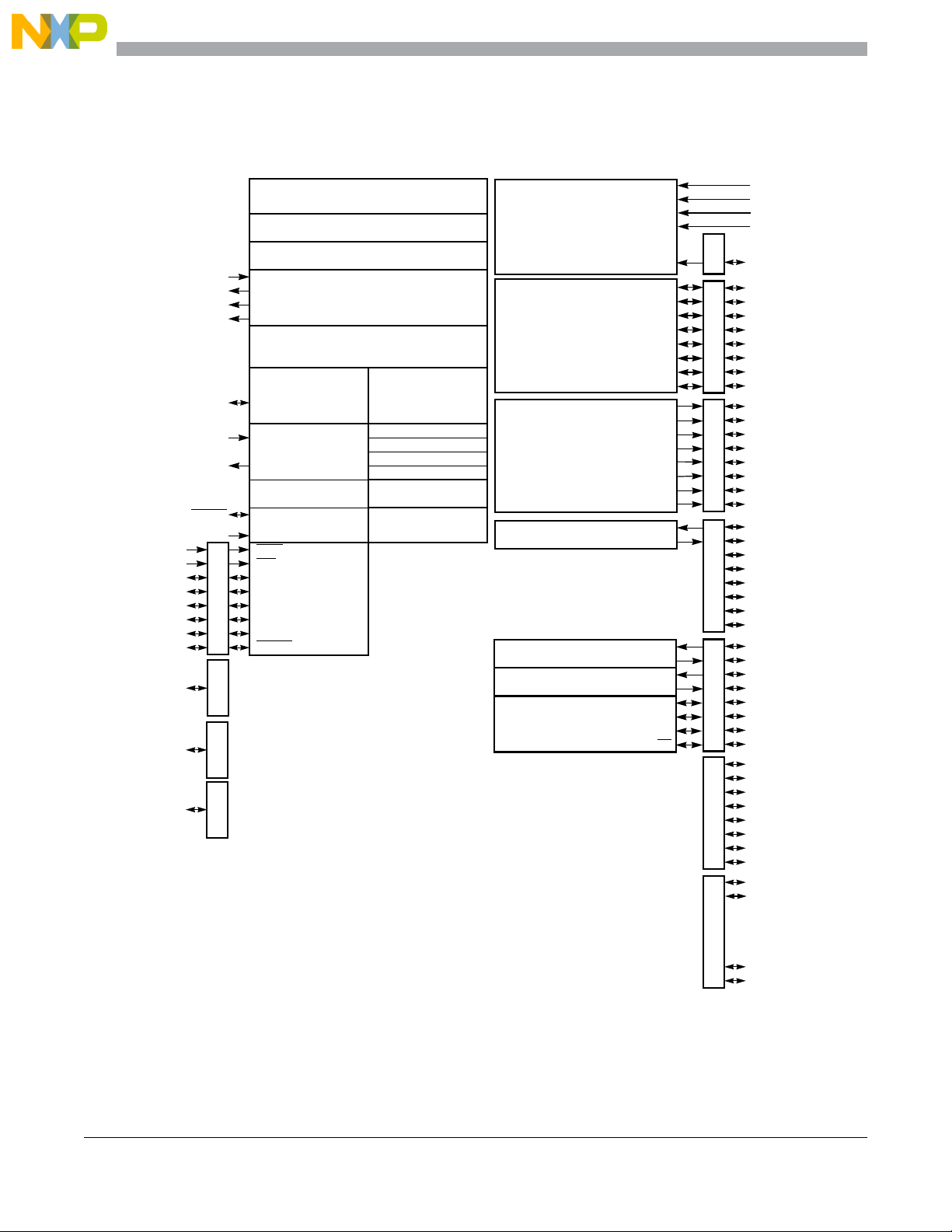
Device Overview S12XS Family
1.1.3 Block Diagram
Figure 1-1 shows a block diagram of the S12XS Family devices
PE0
PE1
PE2
PE3
PE4
PE5
PE6
PE7
PA[7:0]
PB[7:0]
PK[7,5:0]
VDDR
VDD
VDDF
VDDPLL
BKGD
EXTAL
XTAL
RESET
TEST
Single-wire Background
Debug Module
Amplitude Controlled
Low Power Pierce or
Full drive Pierce
Oscillator
PLL with Frequency
Modulation option
Reset Generation
and Test Entry
XIRQ
IRQ
ECLK
PTE
XCLKS/ECLKX2
PTA
PTB
PTK
64, 128, 256 Kbytes Flash
4, 8, 12 Kbytes RAM
4, 8 Kbytes Data Flash
Voltage Regulator
CPU12X
Debug Module
4 address breakpoints
2 data breakpoints
512 Byte Trace Buffer
Clock Monitor
COP Watchdog
Periodic Interrupt
Async. Periodic Int.
PIT
4ch 24-bit Timer
Multilevel
Interrupt Module
ATD
8/10/12-bit 16-channel
Analog-Digital Converter
TIM
16-bit 8 channel
Timer
PWM
8-bit 8 channel
Pulse Width Modulator
CAN0
msCAN 2.0B
SCI0
Asynchronous Serial IF
SCI1
Asynchronous Serial IF
SPI0
Synchronous Serial IF
AN[15:0]
IOC0
IOC1
IOC2
IOC3
IOC4
IOC5
IOC6
IOC7
PWM0
PWM1
PWM2
PWM3
PWM4
PWM5
PWM6
PWM7
RXCAN
TXCAN
RXD
TXD
RXD
TXD
MISO
MOSI
SCK
SS
VDDA
VSSA
VRH
VRL
PAD[15:0]
PTAD
PT0
PT1
PT2
PT3
PT4
PTT
PT5
PT6
PT7
PP0
PP1
PP2
PP3
PP4
PP5
PP6
PTP (Wake-Up Int)
PP7
PM0
PM1
PM2
PM3
PM4
PTM
PM5
PM6
PM7
PS0
PS1
PS2
PS3
PS4
PTS
PS5
PS6
PS7
PH0
PH1
PH2
PH3
PH4
PH5
PH6
PTH (Wake-up Int)
PH7
PJ0
PJ1
PJ6
PTJ (Wake-up Int)
PJ7
Figure 1-1. S12XS Family Block Diagram
S12XS Family Reference Manual, Rev. 1.13
24 Freescale Semiconductor
Page 25

1.1.4 Device Memory Map
Table 1-1 shows the device register memory map.
Table 1-1. Device Register Memory Map
Device Overview S12XS Family
Address Module
0x0000–0x0009 PIM (port integration module
0x000A–0x000B MMC (memory map control) 2
0x000C–0x000D PIM (port integration module) 2
0x000E–0x000F Reserved 2
0x0010–0x0017 MMC (memory map control) 8
0x0018–0x0019 Reserved 2
0x001A–0x001B Device ID register 2
0x001C–0x001F PIM (port integration module) 4
0x0020–0x002F DBG (debug module) 16
0x0030–0x0031 Reserved 2
0x0032–0x0033 PIM (port integration module) 2
0x0034–0x003F ECRG (clock and reset generator) 12
0x0040–0x006F TIM (timer module) 48
0x0070–0x00C7 Reserved 88
0x00C8–0x00CF SCI0 (serial communications interface) 8
0x00D0–0x00D7 SCI1 (serial communications interface) 8
) 10
Size
(Bytes)
0x00D8–0x00DF SPI0 (serial peripheral interface) 8
0x00E0–0x00FF Reserved 32
0x0100–0x0113 FTMR control registers 20
0x0114–0x011F Reserved 12
0x0120–0x012F INT (interrupt module) 16
0x0130–0x013F Reserved 16
0x0140–0x017F CAN0 64
0x0180–0x023F Reserved 192
0x0240–0x027F PIM (port integration module) 64
0x0280–0x02BF Reserved 64
0x02C0–0x02EF ATD0 (analog-to-digital converter 12 bit 16-channel) 48
0x02F0–0x02F7 Voltage regulator 8
0x02F8–0x02FF Reserved 8
0x0300–0x0327 PWM (pulse-width modulator 8 channels) 40
0x0328–0x033F Reserved 24
0x0340–0x0367 PIT (periodic interrupt timer) 40
S12XS Family Reference Manual, Rev. 1.13
Freescale Semiconductor 25
Page 26

Device Overview S12XS Family
Table 1-1. Device Register Memory Map (continued)
Address Module
0x0368–0x07FF Reserved 1176
Size
(Bytes)
NOTE
Reserved register space shown in Table 1-1 is not allocated to any module.
This register space is reserved for future use. Writing to these locations has
no effect. Read access to these locations returns zero.
1.1.5 Address Mapping
Figure 1-2 shows S12XS CPU and BDM local address translation to the global memory map. It indicates
also the location of the internal resources in the memory map.
S12XS Family Reference Manual, Rev. 1.13
26 Freescale Semiconductor
Page 27
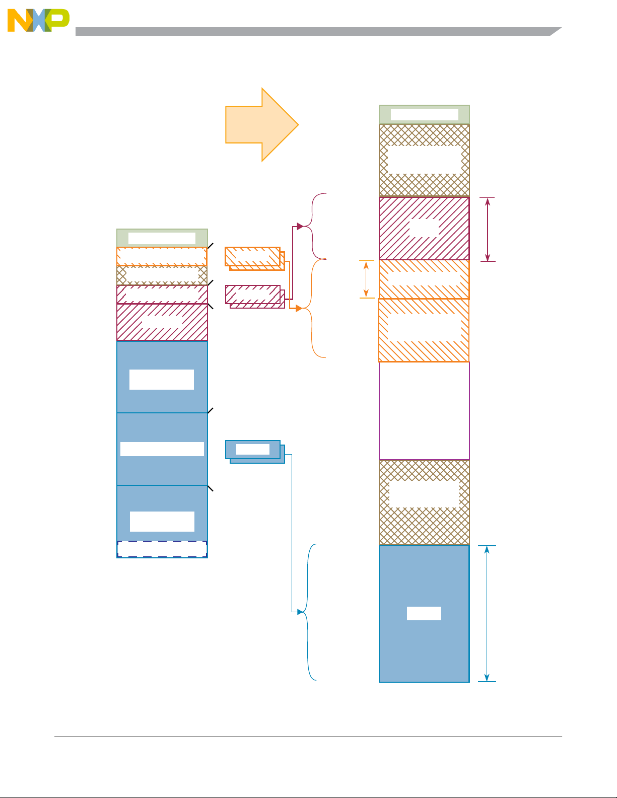
Device Overview S12XS Family
CPU and BDM
Local Memory Map
0x0000
0x0800
0x0C00
0x1000
0x2000
0x4000
2K REGISTERS
1K DFLASH window
Reserved
4K RAM window
8K RAM
Unpaged
16K FLASH
EPAGE
RPAGE
0x00_0000
0x00_07FF
RAM_LOW
0x0F_FFFF
DF_HIGH
0x13_FFFF
Global Memory Map
2K REGISTERS
Unimplemented
RAM
RAM
RAMSIZE
DFLASH
DFLASH
Resources
0x8000
0xC000
0xFFFF
16K FLASH window
Unpaged
16K FLASH
Vectors
Unimplemented
PPAGE
0x3F_FFFF
Unimplemented
FLASH_LOW
0x7F_FFFF
Figure 1-2. S12XS Family Global Memory Map
Space
FLASH
FLASH
FLASHSIZE
S12XS Family Reference Manual, Rev. 1.13
Freescale Semiconductor 27
Page 28
Device Overview S12XS Family
Accessing the reserved area in the range of 0x0C00 to 0x0FFF will return undefined data values.
A CPU access to any unimplemented space causes an illegal address reset.
The range between 0x10_0000 and 0x13_FFFF is mapped to DFLASH (Data Flash). The DFLASH block
sizes are listed in Table 1-2.
Table 1-2. Derivative Dependent Memory Parameters of Device Internal Resources
Device FLASH_LOW
S12XS256 0x7C_0000 256K / 16 0x0F_D000 12K / 3 0x10_1FFF 8K / 8
S12XS128 0x7E_0000 128K / 8 0x0F_E000 8K / 2 0x10_1FFF 8K / 8
S12XS64 0x7F_0000 64K / 4 0x0F_F000 4K / 1 0x10_0FFF 4K / 4
Number of 16K pages addressable via PPAGE register
1
Number of 4K pages addressing the RAM via PPAGE register
2
Number of 1K pages addressing the DFLASH via the EPAGE register starting upwards from 0x00
3
SIZE/
PPAGE
1
RAM_LOW
SIZE/
RPAGE
2
DF_HIGH
SIZE/
EPAGE
3
1.1.6 Detailed Register Map
The detailed register map is listed in the appendix of the reference manual.
1.1.7 Part ID Assignments
The part ID is located in two 8-bit registers PARTIDH and PARTIDL (addresses 0x001A and 0x001B).
The read-only value is a unique part ID for each revision of the chip. Table 1-3 shows the assigned part ID
number and Mask Set number.
The Version ID is a word located in a flash information row at 0x40_00E8. The version ID number
indicates a specific version of internal NVM variables used to patch NVM errata. The default is no patch
(0xFFFF).
Table 1-3. Assigned Part ID Numbers
Device Mask Set Number Part ID
MC9S12XS256 0M05M $C0C0 0xFFFF
MC9S12XS128 0M04M $C1C0 0xFFFF
1M04M $C1C1 0xFFFF
MC9S12XS64 0M04M $C1C0 0xFFFF
1M04M $C1C1 0xFFFF
The coding is as follows:
1
Bit 15-12: Major family identifier
Bit 11-6: Minor family identifier
Bit 5-4: Major mask set revision number including FAB transfers
Bit 3-0: Minor — non full — mask set revision
S12XS Family Reference Manual, Rev. 1.13
28 Freescale Semiconductor
1
Version ID
Page 29

Device Overview S12XS Family
1.2 Signal Description
This section describes signals that connect off-chip. It includes a pinout diagram, a table of signal
properties, and detailed discussion of signals. It is built from the signal description sections of the
individual IP blocks on the device.
1.2.1 Device Pinout
The XS family of devices offers pin-compatible packaged devices to assist with system development and
accommodate expansion of the application.
The S12XS family devices are offered in the following package options:
• 112-pin LQFP
• 80-pin QFP
• 64-pin LQFP
S12XS Family Reference Manual, Rev. 1.13
Freescale Semiconductor 29
Page 30
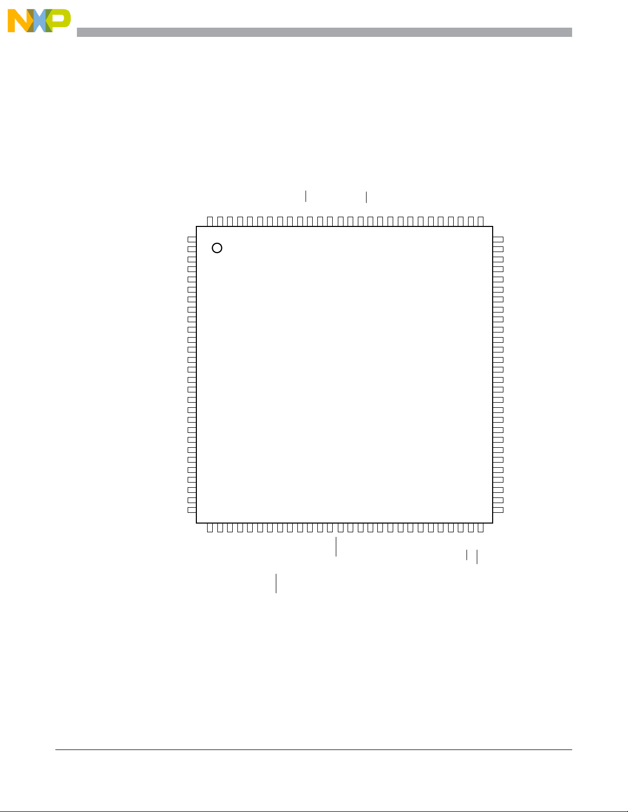
Device Overview S12XS Family
PP4/KWP4/PWM4
PP5/KPW5/PWM5
PP6/KWP6/PWM6
PP7/KWP7/PWM7
PK7
VDDX1
VSSX1
PM0/RXCAN0/RXD1
PM1/TXCAN0/TXD1
PM2/MISO0
PM3/SS0
PM4/MOSI0
PM5/SCK0
PJ6/KWJ6
PJ7/KWJ7
TEST
PS7/SS0
PS6/SCK0
PS5/MOSI0
PS4/MISO0
PS3/TXD1
PS2/RXD1
PS1/TXD0
PS0/RXD0
PM6
PM7
VSSA
VRL
TXD1/IOC2/PWM2/KWP2/PP2
PWM3/KWP3/PP3
IOC1/PWM1/KWP1/PP1
RXD1/IOC0/PWM0/KWP0/PP0
PK3
PK2
PK1
PK0
IOC0/PT0
IOC1/PT1
IOC2/PT2
IOC3/PT3
VDDF
VSS1
PWM4/IOC4/PT4
VREG_API/PWM5/IOC5/PT5
PWM6/IOC6/PT6
PWM7/IOC7/PT7
PK5
PK4
KWJ1/PJ1
KWJ0/PJ0
MODC/BKGD
PB0
PB1
PB2
PB3
PB4
112
111
110
109
108
107
106
105
104
1
103
999897969594939291908988878685
102
101
100
2
3
4
5
6
7
8
9
10
11
S12XS Family
112LQFP
12
13
14
15
16
17
18
19
20
PinsshowninBOLD are not
available on the 80 QFP
package
21
22
23
24
25
26
27
28
293031323334353637383940414243444546474849505152535455
84
83
82
81
80
79
78
77
76
75
74
73
72
71
70
69
68
67
66
65
64
63
62
61
60
59
58
57
VRH
VDDA
PAD15/AN15
PAD07/AN07
PAD14/AN14
PAD06/AN06
PAD13/AN13
PAD05/AN05
PAD12/AN12
PAD04/AN04
PAD11/AN11
PAD03/AN03
PAD10/AN10
PAD02/AN02
PAD09/AN09
PAD01/AN01
PAD08/AN08
PAD00/AN00
VSS2
VDD
PA 7
PA 6
PA 5
PA 4
PA 3
PA 2
PA 1
PA 0
56
PB5
PB6
PB7
KWH7/PH7
KWH6/PH6
KWH5/PH5
KWH4/PH4
XCLKS/ECLKX2/PE7
PE6
PE5
VSSX2
VDDX2
ECLK/PE4
VDDR
RESET
VSS3
EXTAL
VSSPLL
XTAL
VDDPLL
KWH3/PH3
KWH2/PH2
KWH1/PH1
KWH0/PH0
PE3
PE2
IRQ/PE1
XIRQ/PE0
Figure 1-3. S12XS Family Pin Assignments 112-pin LQFP Package
S12XS Family Reference Manual, Rev. 1.13
30 Freescale Semiconductor
Page 31

PP4/KWP4/PWM4
PP5/KPW5/PWM5
PP7/KPW7/PWM7
VDDX1
VSSX1
PM0/RXCAN0/RXD1
PM4/MOSI0
PM5/SCK0
PM3/SS0
PJ6/KWJ6
PM1/TXCAN0/TXD1
PM2/MISO0
PJ7/KWJ7
TEST
PS3/TXD1
PS2/RXD1
PS1/TXD0
PS0/RXD0
Device Overview S12XS Family
VSSA
VRL
TXD1/IOC2/PWM2/KWP2/PP2
PWM3/KWP3/PP3
IOC1/PWM1/KWP1/PP1
RXD1/IOC0/PWM0/KWP0/PP0
IOC0/PT0
IOC1/PT1
IOC2/PT2
IOC3/PT3
VDDF
VSS1
PWM4/IOC4/PT4
VREG_API/PWM5/IOC5/PT5
PWM6/IOC6/PT6
PWM7/IOC7/PT7
MODC/BKGD
PB0
PB1
PB2
PB3
PB4
80797877767574737271706968676665646362
1
2
3
4
5
6
7
8
9
10
11
12
13
14
15
16
17
18
19
20
21222324252627282930313233343536373839
PB5
PB6
S12XS Family
80QFP
Pins shown in BOLD are
not available on the 64
QFP package
PB7
PE6
PE5
ECLK/PE4
XCLKS/ECLKX2/PE7
VSSX2
VDDX2
VDDR
RESET
VSS3
VSSPLL
EXTAL
XTAL
VDDPLL
PE3
PE2
61
60
59
58
57
56
55
54
53
52
51
50
49
48
47
46
45
44
43
42
41
40
IRQ/PE1
XIRQ/PE0
VRH
VDDA
PAD07/AN07
PAD06/AN06
PAD05/AN05
PAD04/AN04
PAD03/AN03
PAD02/AN02
PAD01/AN01
PAD00/AN00
VSS2
VDD
PA 7
PA 6
PA 5
PA 4
PA 3
PA 2
PA 1
PA 0
Figure 1-4. S12XS Family Pin Assignments 80-pin QFP Package
S12XS Family Reference Manual, Rev. 1.13
Freescale Semiconductor 31
Page 32

Device Overview S12XS Family
PP5/KPW5/PWM5
PP7/KWP7/PWM7
VDDX1
VSSX1
PM0/RXCAN0/RXD1
PM1/TXCAN0/TXD1
PM4/MOSI0
PM5/SCK0
PM2/MISO0
PM3/SS0
TEST
PS3/TXD1
PS2/RXD1
PS1/TXD0
PS0/RXD0
VSSA/VRL
TXD1/IOC2/PWM2/KWP2/PP2
PWM3/KWP3/PP3
IOC1/PWM1/KWP1/PP1
RXD1/IOC0/PWM0/KWP0/PP0
IOC0/PT0
IOC1/PT1
IOC2/PT2
IOC3/PT3
VDDF
VSS1
PWM4/IOC4/PT4
VREG_API/PWM5/IOC5/PT5
PWM6/IOC6/PT6
PWM7/IOC7/PT7
MODC/BKGD
PB0
646362616059585756555453525150
1
2
3
4
5
6
7
8
9
10
11
12
13
14
15
16
171819202122232425262728293031
PB5
S12XS Family
64LQFP
PB6
PB7
VSSX2
VDDX2
ECLK/PE4
XCLKS/ECLKX2/PE7
VSS3
VDDR
RESET
XTAL
EXTAL
VSSPLL
49
48
47
46
45
44
43
42
41
40
39
38
37
36
35
34
33
32
IRQ/PE1
XIRQ/PE0
VDDPLL
VRH
VDDA
PAD07/AN07
PAD06/AN06
PAD05/AN05
PAD04/AN04
PAD03/AN03
PAD02/AN02
PAD01/AN01
PAD00/AN00
VSS2
VDD
PA 3
PA 2
PA 1
PA 0
Figure 1-5. S12XS Family Pin Assignments 64-pin LQFP Package
S12XS Family Reference Manual, Rev. 1.13
32 Freescale Semiconductor
Page 33

Device Overview S12XS Family
1.2.2 Pin Assignment Overview
Table 1-4 provides a summary of which ports are available for each package option. Routing of pin
functions is summarized in Table 1-5.
Table 1-4. Port Availability by Package Option
Port 112 LQFP 80 QFP 64 LQFP
Port AD/ADC Channels 16/16 8/8 8/8
Port A pins 8 8 4
Port B pins 8 8 4
Port E pins inc. IRQ/XIRQ input only 8 8 4
Port H 800
Port J 420
Port K 700
Port M 866
Port P 876
Port S 844
Port T 888
Sum of Ports 91 59 44
I/O Power Pairs VDDX/VSSX 2/2 2/2 2/2
Table 1-5. Peripheral - Port Routing Options
SCI1 SPI0 PWM TIM
PM[1:0] O
PM[5:2] O
PP[2,0] O
PP[2:0] O
PP[7:4] X
PS[3:2] X
PS[7:4] X
PT[2:0] X
1
PT[7:4] O
“X” denotes reset condition, “O” denotes a possiblererouting
1
under software control
S12XS Family Reference Manual, Rev. 1.13
Freescale Semiconductor 33
Page 34

34 Freescale Semiconductor
Table 1-6 provides a pin out summary listing the availability and functionality of individual pins for each package option.
Device Overview S12XS Family
S12XS Family Reference Manual, Rev. 1.13
Table 1-6. Pin-Out Summary
Package Terminal Function
LQFP
112
QFP80LQFP
64
Pin
2nd
Func.
3rd
Func.
4th
Func.
5th
Func.
1 1 1 PP3 KWP3 PWM3 — — V
1
Power
Supply
DDX
Internal Pull
Resistor
Description
CTRL
Reset
State
PERP/PPSP Disabled Port P I/O, interrupt,
PWM channel
2 2 2 PP2 KWP2 PWM2 IOC2 TXD1 V
DDX
PERP/PPSP Disabled Port P I/O, interrupt,
PWM/TIMchannel,TXD
of SCI1
3 3 3 PP1 KWP1 PWM1 IOC1 — V
DDX
PERP/PPSP Disabled Port P I/O, interrupt,
PWM/TIM channel
4 4 4 PP0 KWP0 PWM0 IOC0 RXD1 V
DDX
PERP/PPSP Disabled Port P I/O, interrupt,
PWM/TIM channel,
RXD of SCI1
5 - - PK3 — — — — V
6 - - PK2 — — — — V
7 - - PK1 — — — — V
8 - - PK0 — — — — V
9 5 5 PT0 IOC0 — — — V
10 6 6 PT1 IOC1 — — — V
11 7 7 PT2 IOC2 — — — V
12 8 8 PT3 IOC3 — — — V
DDX
DDX
DDX
DDX
DDX
DDX
DDX
DDX
PUCR Up Port K I/O
PUCR Up Port K I/O
PUCR Up Port K I/O
PUCR Up Port K I/O
PERT/PPST Disabled Port T I/O, TIM channel
PERT/PPST Disabled Port T I/O, TIM channel
PERT/PPST Disabled Port T I/O, TIM channel
PERT/PPST Disabled Port T I/O, TIM channel
13 9 9 VDDF — — — — — — — —
14 10 10 VSS1 — — — — — — — —
15 11 11 PT4 IOC4 PWM4 — — V
DDX
PERT/PPST Disabled Port T I/O, PWM/TIM
channel
Page 35

Freescale Semiconductor 35
Table 1-6. Pin-Out Summary1 (continued)
S12XS Family Reference Manual, Rev. 1.13
Package Terminal Function
LQFP
112
QFP80LQFP
64
Pin
2nd
Func.
3rd
Func.
4th
Func.
16 12 12 PT5 IOC5 PWM5 VREG_
5th
Func.
—V
API
17 13 13 PT6 IOC6 PWM6 — — V
18 14 14 PT7 IOC7 PWM7 — — V
19 - - PK5 — — — — V
20 - - PK4 — — — — V
21 - - PJ1 KWJ1 — — — V
22 - - PJ0 KWJ0 — — — V
23 15 15 BKGD MODC — — — V
24 16 16 PB0 — — — — V
25 17 - PB1 — — — — V
26 18 - PB2 — — — — V
27 19 - PB3 — — — — V
28 20 - PB4 — — — — V
29 21 17 PB5 — — — — V
30 22 18 PB6 — — — — V
31 23 19 PB7 — — — — V
32 - - PH7 KWH7 — — — V
33 - - PH6 KWH6 — — — V
34 - - PH5 KWH5 — — — V
35 - - PH4 KWH4 — — — V
Power
Supply
DDX
DDX
DDX
DDX
DDX
DDX
DDX
DDX
DDX
DDX
DDX
DDX
DDX
DDX
DDX
DDX
DDX
DDX
DDX
DDX
Internal Pull
Resistor
Description
CTRL
Reset
State
PERT/PPST Disabled Port T I/O, PWM/TIM
channel, API output
PERT/PPST Disabled Port T I/O, channel of
PWM/TIM
PERT/PPST Disabled Port T I/O, channel of
PWM/TIM
PUCR Up Port K I/O
PUCR Up Port K I/O
PERJ/PPSJ Up Port J I/O, interrupt
PERJ/PPSJ Up Port J I/O, interrupt
Always on Up Background debug
PUCR Disabled Port B I/O
PUCR Disabled Port B I/O
PUCR Disabled Port B I/O
PUCR Disabled Port B I/O
PUCR Disabled Port B I/O
PUCR Disabled Port B I/O
PUCR Disabled Port B I/O
PUCR Disabled Port B I/O
PERH/PPSH Disabled Port H I/O, interrupt
PERH/PPSH Disabled Port H I/O, interrupt
PERH/PPSH Disabled Port H I/O, interrupt
PERH/PPSH Disabled Port H I/O, interrupt
Device Overview S12XS Family
Page 36

36 Freescale Semiconductor
Table 1-6. Pin-Out Summary1 (continued)
Device Overview S12XS Family
S12XS Family Reference Manual, Rev. 1.13
Package Terminal Function
LQFP
112
QFP80LQFP
64
Pin
2nd
Func.
3rd
Func.
4th
Func.
5th
Func.
36 24 20 PE7 XCLKS ECLKX2 — — V
Power
Supply
DDX
Internal Pull
Resistor
Description
CTRL
Reset
State
PUCR Up Port E I/O,system clock
output, clock select
input
37 25 - PE6 — — — — V
38 26 - PE5 — — — — V
39 27 21 PE4 ECLK — — — V
DDX
DDX
DDX
While RESET pin
is low: down
While RESET pin
is low: down
2
2
Port E I/O
Port E I/O
PUCR Up Port E I/O, bus clock
output
40 28 22 VSSX2 — — — — — — — —
41 29 23 VDDX2 — — — — — — — —
42 30 24
RESET — — — — V
DDX
PULLUP External reset
43 31 25 VDDR — — — — — — — —
44 32 26 VSS3 — — — — — — — —
45 33 27 VSSPLL — — — — — — — —
46 34 28 EXTAL — — — — V
47 35 29 XTAL — — — — V
DDPLL
DDPLL
NA NA Oscillator pin
NA NA Oscillator pin
48 36 30 VDDPLL — — — — — — — —
49 - - PH3 KWH3 — — — V
50 - - PH2 KWH2 — — — V
51 - - PH1 KWH1 — — — V
52 - - PH0 KWH0 — — — V
53 37 - PE3 — — — — V
54 38 - PE2 — — — — V
DDX
DDX
DDX
DDX
DDX
DDX
PERH/PPSH Disabled Port H I/O, interrupt
PERH/PPSH Disabled Port H I/O, interrupt
PERH/PPSH Disabled Port H I/O, interrupt
PERH/PPSH Disabled Port H I/O, interrupt
PUCR Up Port E I/O
PUCR Up Port E I/O
Page 37

Freescale Semiconductor 37
Table 1-6. Pin-Out Summary1 (continued)
S12XS Family Reference Manual, Rev. 1.13
Package Terminal Function
LQFP
112
QFP80LQFP
64
Pin
2nd
Func.
3rd
Func.
4th
Func.
5th
Func.
55 39 31 PE1 IRQ — — — V
Power
Supply
DDX
Internal Pull
Resistor
Description
CTRL
Reset
State
PUCR Up Port E Input, maskable
interrupt
56 40 32 PE0
XIRQ — — — V
DDX
PUCR Up Port E Input, non-
maskable interrupt
57 41 33 PA0 — — — — V
58 42 34 PA1 — — — — V
59 43 35 PA2 — — — — V
60 44 36 PA3 — — — — V
61 45 - PA4 — — — — V
62 46 - PA5 — — — — V
63 47 - PA6 — — — — V
64 48 - PA7 — — — — V
DDX
DDX
DDX
DDX
DDX
DDX
DDX
DDX
PUCR Disabled Port A I/O
PUCR Disabled Port A I/O
PUCR Disabled Port A I/O
PUCR Disabled Port A I/O
PUCR Disabled Port A I/O
PUCR Disabled Port A I/O
PUCR Disabled Port A I/O
PUCR Disabled Port A I/O
65 49 37 VDD — — — — — — — —
66 50 38 VSS2 — — — — — — — —
67 51 39 PAD00 AN00 — — — V
DDA
PER1AD Disabled Port AD I/O,
analog input of ATD
68 - - PAD08 AN08 — — — V
DDA
PER0AD Disabled Port AD I/O,
analog input of ATD
69 52 40 PAD01 AN01 — — — V
DDA
PER1AD Disabled Port AD I/O,
analog input of ATD
70 - - PAD09 AN09 — — — V
DDA
PER0AD Disabled Port AD I/O,
analog input of ATD
71 53 41 PAD02 AN02 — — — V
DDA
PER1AD Disabled Port AD I/O,
analog input of ATD
Device Overview S12XS Family
Page 38

38 Freescale Semiconductor
Table 1-6. Pin-Out Summary1 (continued)
Device Overview S12XS Family
S12XS Family Reference Manual, Rev. 1.13
Package Terminal Function
LQFP
112
QFP80LQFP
64
Pin
2nd
Func.
3rd
Func.
4th
Func.
5th
Func.
72 - - PAD10 AN10 — — — V
73 54 42 PAD03 AN03 — — — V
74 - - PAD11 AN11 — — — V
75 55 43 PAD04 AN04 — — — V
76 - - PAD12 AN12 — — — V
77 56 44 PAD05 AN05 — — — V
78 - - PAD13 AN13 — — — V
79 57 45 PAD06 AN06 — — — V
Power
Supply
DDA
DDA
DDA
DDA
DDA
DDA
DDA
DDA
Internal Pull
Resistor
Description
CTRL
Reset
State
PER0AD Disabled Port AD I/O,
analog input of ATD
PER1AD Disabled Port AD I/O,
analog input of ATD
PER0AD Disabled Port AD I/O,
analog input of ATD
PER1AD Disabled Port AD I/O,
analog input of ATD
PER0AD Disabled Port AD I/O,
analog input of ATD
PER1AD Disabled Port AD I/O,
analog input of ATD
PER0AD Disabled Port AD I/O,
analog input of ATD
PER1AD Disabled Port AD I/O,
analog input of ATD
80 - - PAD14 AN14 — — — V
DDA
PER0AD Disabled Port AD I/O,
analog input of ATD
81 58 46 PAD07 AN07 — — — V
DDA
PER1AD Disabled Port AD I/O,
analog input of ATD
82 - - PAD15 AN15 — — — V
DDA
PER0AD Disabled Port AD I/O,
analog input of ATD
83 59 47 VDDA — — — — — — — —
84 60 48 VRH — — — — — — — —
85 61 49 VRL
3
————— — — —
86 62 49 VSSA — — — — — — — —
Page 39

Freescale Semiconductor 39
Table 1-6. Pin-Out Summary1 (continued)
S12XS Family Reference Manual, Rev. 1.13
Package Terminal Function
Power
LQFP
112
QFP80LQFP
64
Pin
2nd
Func.
3rd
Func.
4th
Func.
5th
Func.
Supply
87 - - PM7 — — — — V
88 - - PM6 — — — — V
89 63 50 PS0 RXD0 — — — V
90 64 51 PS1 TXD0 — — — V
91 65 52 PS2 RXD1 — — — V
92 66 53 PS3 TXD1 — — — V
93 - - PS4 MISO0 — — — V
94 - - PS5 MOSI0 — — — V
95 - - PS6 SCK0 — — — V
96 - - PS7
SS0 — — — V
97 67 54 TEST — — — — N.A.
98 68 - PJ7 KWJ7 — — — V
99 69 - PJ6 KWJ6 — — — V
100 70 55 PM5 SCK0 — — — V
101 71 56 PM4 MOSI0 — — — V
102 72 57 PM3
SS0 — — — V
103 73 58 PM2 MISO0 — — — V
DDX
DDX
DDX
DDX
DDX
DDX
DDX
DDX
DDX
DDX
DDX
DDX
DDX
DDX
DDX
DDX
Internal Pull
Resistor
Description
CTRL
Reset
State
PERM/PPSM Disabled Port M I/O
PERM/PPSM Disabled Port M I/O
PERS/PPSS Up Port S I/O, RXD of SCI0
PERS/PPSS Up Port S I/O, TXD of SCI0
PERS/PPSS Up Port S I/O, RXD of SCI1
PERS/PPSS Up Port S I/O, TXD of SCI1
PERS/PPSS Up PortS I/O, MISO of SPI0
PERS/PPSS Up PortS I/O, MOSI of SPI0
PERS/PPSS Up Port S I/O, SCK of SPI0
PERS/PPSS Up Port S I/O, SS of SPI0
RESET pin DOWN Test input
PERJ/PPSJ Up Port J I/O, interrupt
PERJ/PPSJ Up Port J I/O, interrupt
PERM/PPSM Disabled Port M I/O, SCK of SPI0
PERM/PPSM Disabled Port M I/O, MOSI of
SPI0
PERM/PPSM Disabled Port M I/O, SS of SPI0
PERM/PPSM Disabled Port M I/O, MISO of
SPI0
Device Overview S12XS Family
104 74 59 PM1 TXCAN0 TXD1 — — V
105 75 60 PM0 RXCAN0 RXD1 — — V
DDX
DDX
PERM/PPSM Disabled Port M I/O,TX of CAN0,
TXD of SCI1
PERM/PPSM Disabled Port M I/O, RX of CAN0,
RXD of SCI1
Page 40

40 Freescale Semiconductor
Table 1-6. Pin-Out Summary1 (continued)
Device Overview S12XS Family
S12XS Family Reference Manual, Rev. 1.13
Package Terminal Function
LQFP
112
QFP80LQFP
64
Pin
2nd
Func.
3rd
Func.
4th
Func.
5th
Func.
Power
Supply
Internal Pull
Resistor
CTRL
Description
Reset
State
106 76 61 VSSX1 — — — — — — — —
107 77 62 VDDX1 — — — — — — — —
108 - - PK7 — — — — V
109 78 63 PP7 KWP7 PWM7 — — V
DDX
DDX
PUCR Up Port K I/O
PERP/PPSP Disabled Port P I/O, interrupt,
PWM channel
110 - - PP6 KWP6 PWM6 — — V
DDX
PERP/PPSP Disabled Port P I/O, interrupt,
PWM channel
111 79 64 PP5 KWP5 PWM5 — — V
DDX
PERP/PPSP Disabled Port P I/O, interrupt,
PWM channel
112 80 - PP4 KWP4 PWM4 — — V
DDX
PERP/PPSP Disabled Port P I/O, interrupt,
PWM channel
Table shows a superset of pin functions. Not all functions are available on all derivatives
1
For compatibility to XE family
2
VRL and VSSA share single pin on 64 package option
3
Page 41

Device Overview S12XS Family
1.2.3 Detailed Signal Descriptions
NOTE
The pin list of the largest package version of each S12XS Family derivative
gives the complete of interface signals that also exist on smaller package
options, although some of them are not bonded out. For devices assembled
in smaller packages all non-bonded out pins should be configured as outputs
after reset in order to avoid current drawn from floating inputs. Refer to
Table 1-6 for affected pins.
1.2.3.1 EXTAL, XTAL — Oscillator Pins
EXTAL and XTAL are the crystal driver and external clock pins. On reset all the device clocks are derived
from the EXTAL input frequency. XTAL is the oscillator output.
1.2.3.2 RESET — External Reset Pin
The RESET pin is an active low bidirectional control signal. It acts as an input to initialize the MCU to a
known start-up state. As an output it is driven low to indicate when any internal MCU reset source triggers.
RESET pin has an internal pull-up device.
The
1.2.3.3 TEST — Test Pin
This input only pin is reserved for factory test. This pin has a pull-down device.
NOTE
The TEST pin must be tied to V
in all applications.
SS
1.2.3.4 BKGD / MODC — Background Debug and Mode Pin
The BKGD/MODC pin is used as a pseudo-open-drain pin for the background debug communication. It
is used as a MCU operating mode select pin during reset. The state of this pin is latched to the MODC bit
at the rising edge of
RESET. The BKGD pin has an internal pull-up device.
1.2.3.5 PAD[15:0] / AN[15:0] — Port AD Input Pins of ATD0
PAD[15:0] are general-purpose input or output pins and analog inputs AN[15:0] of the analog-to-digital
converter ATD0.
1.2.3.6 PA[7:0] — Port A I/O Pins
PA[7:0] are general-purpose input or output pins.
1.2.3.7 PB[7:0] — Port B I/O Pins
PB[7:0] are general-purpose input or output pins.
S12XS Family Reference Manual, Rev. 1.13
Freescale Semiconductor 41
Page 42

Device Overview S12XS Family
1.2.3.8 PE7 / ECLKX2 / XCLKS — Port E I/O Pin 7
PE7 is a general-purpose input or output pin. ECLKX2 is a clock output of twice the internal bus
frequency. The
loop controlled Pierce oscillator is used or whether full swing Pierce oscillator/external clock circuitry is
used (refer to Section 1.10 Oscillator Configuration). An internal pull-up is enabled during reset.
XCLKS is an input signal which controls whether a crystal in combination with the internal
1.2.3.9 PE[6:5] — Port E I/O Pin 6-5
PE[6:5] are a general-purpose input or output pins.
1.2.3.10 PE4 / ECLK — Port E I/O Pin 4
PE4 is a general-purpose input or output pin. It can be configured to output the internal bus clock ECLK.
ECLK can be used as a timing reference. The ECLK output has a programmable prescaler.
1.2.3.11 PE[3:2] — Port E I/O Pin 3
PE[3:2] are a general-purpose input or output pins.
1.2.3.12 PE1 / IRQ — Port E Input Pin 1
PE1 is a general-purpose input pin and the maskable interrupt request input that provides a means of
applying asynchronous interrupt requests. This will wake up the MCU from stop or wait mode.
1.2.3.13 PE0 / XIRQ — Port E Input Pin 0
PE0 is a general-purpose input pin and the non-maskable interrupt request input that provides a means of
applying asynchronous interrupt requests. This will wake up the MCU from stop or wait mode. The XIRQ
interrupt is level sensitive and active low. As XIRQ is level sensitive, while this pin is low the MCU will
not enter STOP mode.
1.2.3.14 PH[7:0] / KWH[7:0] — Port H I/O Pins
PH[7:0] are a general-purpose input or output pins. They can be configured as keypad wakeup inputs.
1.2.3.15 PJ[7:6] / KWJ[7:6] — PORT J I/O Pins 7-6
PJ[7:6] are a general-purpose input or output pins. They can be configured as keypad wakeup inputs.
1.2.3.16 PJ[1:0] / KWJ[1:0] — PORT J I/O Pins 1-0
PJ[1:0] are a general-purpose input or output pins. They can be configured as keypad wakeup inputs.
1.2.3.17 PK[7,5:0] — Port K I/O Pins 7 and 5-0
PK[7,5:0] are a general-purpose input or output pins.
S12XS Family Reference Manual, Rev. 1.13
42 Freescale Semiconductor
Page 43

Device Overview S12XS Family
1.2.3.18 PM[7:6] — Port M I/O Pins 7-6
PM[7:6] are a general-purpose input or output pins.
1.2.3.19 PM5 / SCK0 — Port M I/O Pin 5
PM5 is a general-purpose input or output pin. It can be configured as the serial clock pin SCK of the serial
peripheral interface 0 (SPI0).
1.2.3.20 PM4 / MOSI0 — Port M I/O Pin 4
PM4 is a general-purpose input or output pin. It can be configured as the master output (during master
mode) or slave input pin (during slave mode) MOSI for the serial peripheral interface 0 (SPI0).
1.2.3.21 PM3 / SS0 — Port M I/O Pin 3
PM3 is a general-purpose input or output pin. It can be configured as the slave select pin SS of the serial
peripheral interface 0 (SPI0).
1.2.3.22 PM2 / MISO0 — Port M I/O Pin 2
PM2 is a general-purpose input or output pin. It can be configured as the master input (during master
mode) or slave output pin (during slave mode) MISO for the serial peripheral interface 0 (SPI0).
1.2.3.23 PM1 / TXCAN0 / TXD1 — Port M I/O Pin 1
PM1 is a general-purpose input or output pin. It can be configured as the transmit pin TXCAN of the
scalable controller area network controller 0 (CAN0). It can be configured as the transmit pin TXD of
serial communication interface 1 (SCI1).
1.2.3.24 PM0 / RXCAN0 / RXD1 — Port M I/O Pin 0
PM0 is a general-purpose input or output pin. It can be configured as the receive pin RXCAN of the
scalable controller area network controller 0 (CAN0). It can be configured as the receive pin RXD of serial
communication interface 1 (SCI1).
1.2.3.25 PP7 / KWP7 / PWM7 — Port P I/O Pin 7
PP7 is a general-purpose input or output pin. It can be configured as keypad wakeup input. It can be
configured as pulse width modulator (PWM) channel 7 output or emergency shutdown input.
1.2.3.26 PP[6:3] / KWP[6:3] / PWM[6:3] — Port P I/O Pins 6-3
PP[6:3] are a general-purpose input or output pins. They can be configured as keypad wakeup inputs. They
can be configured as pulse width modulator (PWM) channel 6-3 output.
S12XS Family Reference Manual, Rev. 1.13
Freescale Semiconductor 43
Page 44

Device Overview S12XS Family
1.2.3.27 PP2 / KWP2 / PWM2 / TXD1 / IOC2 — Port P I/O Pin 2
PP2 is a general-purpose input or output pin. It can be configured as a keypad wakeup input. It can be
configured as pulse width modulator (PWM) channel 2 output, TIM channel 2 or as the transmit pin TXD
of serial communication interface 1 (SCI1).
1.2.3.28 PP1 / KWP1 / PWM1 / IOC1 — Port P I/O Pin 1
PP1 is a general-purpose input or output pin. It can be configured as a keypad wakeup input. It can be
configured as pulse width modulator (PWM) channel 1 output, TIM channel 1.
1.2.3.29 PP0 / KWP0 / PWM0 / RXD1 / IOC0 — Port P I/O Pin 0
PP0 is a general-purpose input or output pin. It can be configured as a keypad wakeup input. It can be
configured as pulse width modulator (PWM) channel 0 output, TIM channel 0 or as the receive pin RXD
of serial communication interface 1 (SCI1).
1.2.3.30 PS7 / SS0 — Port S I/O Pin 7
PS7 is a general-purpose input or output pin. It can be configured as the slave select pin SS of the serial
peripheral interface 0 (SPI0).
1.2.3.31 PS6 / SCK0 — Port S I/O Pin 6
PS6 is a general-purpose input or output pin. It can be configured as the serial clock pin SCK of the serial
peripheral interface 0 (SPI0).
1.2.3.32 PS5 / MOSI0 — Port S I/O Pin 5
PS5 is a general-purpose input or output pin. It can be configured as master output (during master mode)
or slave input pin (during slave mode) MOSI of the serial peripheral interface 0 (SPI0).
1.2.3.33 PS4 / MISO0 — Port S I/O Pin 4
PS4 is a general-purpose input or output pin. It can be configured as master input (during master mode) or
slave output pin (during slave mode) MOSI of the serial peripheral interface 0 (SPI0).
1.2.3.34 PS3 / TXD1 — Port S I/O Pin 3
PS3 is a general-purpose input or output pin. It can be configured as the transmit pin TXD of serial
communication interface 1 (SCI1).
1.2.3.35 PS2 / RXD1 — Port S I/O Pin 2
PS2 is a general-purpose input or output pin. It can be configured as the receive pin RXD of serial
communication interface 1 (SCI1).
S12XS Family Reference Manual, Rev. 1.13
44 Freescale Semiconductor
Page 45

Device Overview S12XS Family
1.2.3.36 PS1 / TXD0 — Port S I/O Pin 1
PS1 is a general-purpose input or output pin. It can be configured as the transmit pin TXD of serial
communication interface 0 (SCI0).
1.2.3.37 PS0 / RXD0 — Port S I/O Pin 0
PS0 is a general-purpose input or output pin. It can be configured as the receive pin RXD of serial
communication interface 0 (SCI0).
1.2.3.38 PT[7:6] / IOC[7:6] / PWM[7:6] — Port T I/O Pins 7-6
PT[7:6] are general-purpose input or output pins. They can be configured as timer (TIM) channel 7-6 or
pulse width modulator (PWM) outputs 7-6
1.2.3.39 PT5 / IOC5 / VREG_API — Port T I/O Pin 5
PT[5] is a general-purpose input or output pin. It can be configured as timer (TIM) channel 5, pulse width
modulator (PWM) output 5 or as the VREG_API signal output.
1.2.3.40 PT4 / IOC4 / PWM4 — Port T I/O Pin 4
PT4 is a general-purpose input or output pin. It can be configured as timer (TIM) channel 4 or pulse width
modulator (PWM) output 4.
1.2.3.41 PT[3:0] / IOC[3:0] — Port T I/O Pin [3:0]
PT[3:0] are a general-purpose input or output pins. They can be configured as timer (TIM) channels 3-0.
1.2.4 Power Supply Pins
S12XS Family power and ground pins are described below.
Because fast signal transitions place high, short-duration current demands on the power supply, use bypass
capacitors with high-frequency characteristics and place them as close to the MCU as possible.
NOTE
All V
1.2.4.1 VDDX[2:1], VSSX[2:1] — Power and Ground Pins for I/O Drivers
External power and ground for I/O drivers. Bypass requirements depend on how heavily the MCU pins are
loaded. All V
DDX
pins must be connected together in the application.
SS
pins are connected together internally. All V
SSX
pins are connected together internally.
1.2.4.2 VDDR — Power Pin for Internal Voltage Regulator
Power supply input to the internal voltage regulator.
S12XS Family Reference Manual, Rev. 1.13
Freescale Semiconductor 45
Page 46

Device Overview S12XS Family
1.2.4.3 VDD, VSS2, VSS3 — Core Power Pins
The voltage supply of nominally 1.8 V is derived from the internal voltage regulator. The return current
path is through the VSS2 and VSS3 pins. No static external loading of these pins is permitted.
1.2.4.4 VDDF, VSS1 — NVM Power Pins
The voltage supply of nominally 2.8 V is derived from the internal voltage regulator. The return current
path is through the VSS1 pin. No static external loading of these pins is permitted.
1.2.4.5 VDDA, VSSA — Power Supply Pins for ATD and Voltage Regulator
These are the power supply and ground input pins for the analog-to-digital converters and the voltage
regulator.
1.2.4.6 VRH, VRL — ATD Reference Voltage Input Pins
VRH and VRL are the reference voltage input pins for the analog-to-digital converter.
1.2.4.7 VDDPLL, VSSPLL — Power Supply Pins for PLL
These pins provide operating voltage and ground for the oscillator and the phased-locked loop. The voltage
supply of nominally 1.8 V is derived from the internal voltage regulator. This allows the supply voltage to
the oscillator and PLL to be bypassed independently. This voltage is generated by the internal voltage
regulator. No static external loading of these pins is permitted.
Table 1-7. Power and Ground Connection Summary
Mnemonic
VDDR 5.0 V External power supply to internal voltage
VDDX[2:1] 5.0 V External power and ground, supply to pin
VSSX[2:1] 0 V
VDDA 5.0 V Operating voltage and ground for the
VSSA 0 V
VRL 0 V Referencevoltages for the analog-to-digital
VRH 5.0 V
VDD 1.8 V Internal power and ground generated by
VSS1, VSS2,
VSS3
Nominal
Voltage
0 V
Description
regulator
drivers
analog-to-digital converters and the
reference for the internal voltage regulator,
allows the supply voltage to the A/D to be
bypassed independently.
converter.
internal regulator for the internal core.
VDDF 2.8 V Internal power and ground generated by
internal regulator for the internal NVM.
S12XS Family Reference Manual, Rev. 1.13
46 Freescale Semiconductor
Page 47

Device Overview S12XS Family
Table 1-7. Power and Ground Connection Summary
Mnemonic
VDDPLL 1.8 V Provides operating voltage and ground for
VSSPLL 0 V
Nominal
Voltage
Description
the phased-locked loop. This allows the
supply voltage to the PLL to be bypassed
independently. Internal power and ground
generated by internal regulator.
S12XS Family Reference Manual, Rev. 1.13
47 Freescale Semiconductor
Page 48

Device Overview S12XS Family
1.3 System Clock Description
The clock and reset generator module (CRG) provides the internal clock signals for the core and all
peripheral modules. Figure 1-6 shows the clock connections from the CRG to all modules.
Consult the S12XECRG section for details on clock generation.
NOTE
The XS family uses the XE family clock and reset generator module.
Therefore all CRG references are related to S12XECRG.
SCI0 . . SCI 1
SPI0
CAN0
ATD0
Bus Clock
PIT
EXTAL
CRG
XTAL
Core Clock
RAM S12X FLASH
Figure 1-6. Clock Connections
Oscillator Clock
TIM
PIM
PWM
The system clock can be supplied in several ways enabling a range of system operating frequencies to be
supported:
• The on-chip phase locked loop (PLL)
• the PLL self clocking
• the oscillator
S12XS Family Reference Manual, Rev. 1.13
48 Freescale Semiconductor
Page 49

Device Overview S12XS Family
The clock generated by the PLL or oscillator provides the main system clock frequencies core clock and
bus clock. As shown in Figure 1-6, these system clocks are used throughout the MCU to drive the core,
the memories, and the peripherals.
The program Flash memory is supplied by the bus clock and the oscillator clock. The oscillator clock is
used as a time base to derive the program and erase times for the NVMs.
The CAN modules may be configured to have their clock sources derived either from the bus clock or
directly from the oscillator clock. This allows the user to select its clock based on the required jitter
performance.
In order to ensure the presence of the clock the MCU includes an on-chip clock monitor connected to the
output of the oscillator. The clock monitor can be configured to invoke the PLL self-clocking mode or to
generate a system reset if it is allowed to time out as a result of no oscillator clock being present.
In addition to the clock monitor, the MCU also provides a clock quality checker which performs a more
accurate check of the clock. The clock quality checker counts a predetermined number of clock edges
within a defined time window to insure that the clock is running. The checker can be invoked following
specific events such as on wake-up or clock monitor failure.
1.4 Modes of Operation
The MCU can operate in different modes. These are described in 1.4.1 Chip Configuration Summary.
The MCU can operate in different power modes to facilitate power saving when full system performance
is not required. These are described in 1.4.2 Power Modes.
Some modules feature a software programmable option to freeze the module status whilst the background
debug module is active to facilitate debugging. This is described in 1.4.3 Freeze Mode.
1.4.1 Chip Configuration Summary
The different modes and the security state of the MCU affect the debug features (enabled or disabled).
The operating mode out of reset is determined by the state of the MODC signal during reset (see Table 1-
8). The MODC bit in the MODE register shows the current operating mode and provides limited mode
switching during operation. The state of the MODC signal is latched into this bit on the rising edge of
RESET.
Table 1-8. Chip Modes
Chip Modes MODC
Normal single chip 1
Special single chip 0
1.4.1.1 Normal Single-Chip Mode
This mode is intended for normal device operation. The opcode from the on-chip memory is being
executed after reset (requires the reset vector to be programmed correctly). The processor program is
executed from internal memory.
S12XS Family Reference Manual, Rev. 1.13
Freescale Semiconductor 49
Page 50

Device Overview S12XS Family
1.4.1.2 Special Single-Chip Mode
This mode is used for debugging single-chip operation, boot-strapping, or security related operations. The
background debug module BDM is active in this mode. The CPU executes a monitor program located in
an on-chip ROM. BDM firmware waits for additional serial commands through the BKGD pin.
1.4.2 Power Modes
The MCU features two main low-power modes. Consult the respective section for module specific
behavior in system stop, system pseudo stop, and system wait mode. An important source of information
about the clock system is the Clock and Reset Generator section (CRG).
1.4.2.1 System Stop Modes
The system stop modes are entered if the CPU executes the STOP instruction unless an NVM command
is active. Depending on the state of the PSTP bit in the CLKSEL register the MCU goes into pseudo stop
mode or full stop mode. Please refer to CRG section. Asserting
that is not masked exits system stop modes. System stop modes can be exited by CPU activity, depending
on the configuration of the interrupt request.
If the CPU executes the STOP instruction whilst an NVM command is being processed, then the system
clocks continue running until NVM activity is completed. If a non-masked interrupt occurs within this time
then the system does not effectively enter stop mode although the STOP instruction has been executed.
RESET, XIRQ, IRQ or any other interrupt
1.4.2.2 Full Stop Mode
The oscillator is stopped in this mode. By default all clocks are switched off and all counters and dividers
remain frozen. The Autonomous Periodic Interrupt (API) and ATD module may be enabled to self wake
the device. A Fast wake up mode is available to allow the device to wake from Full Stop mode immediately
on the PLL internal clock without starting the oscillator clock.
1.4.2.3 Pseudo Stop Mode
In this mode the system clocks are stopped but the oscillator is still running and the real time interrupt
(RTI) and watchdog (COP), API and ATD modules may be enabled. Other peripherals are turned off. This
mode consumes more current than system stop mode but, as the oscillator continues to run, the full speed
wake up time from this mode is significantly shorter.
1.4.2.4 Wait Mode
This mode is entered when the CPU executes the WAI instruction. In this mode the CPU will not execute
instructions. The internal CPU clock is switched off. All peripherals can be active in system wait mode.
For further power consumption the peripherals can individually turn off their local clocks. Asserting
RESET, XIRQ, IRQ or any other interrupt that is not masked ends system wait mode.
S12XS Family Reference Manual, Rev. 1.13
50 Freescale Semiconductor
Page 51

Device Overview S12XS Family
1.4.2.5 Run Mode
Although this is not a low-power mode, unused peripheral modules should not be enabled in order to save
power.
1.4.3 Freeze Mode
The timer module, pulse width modulator, analog-to-digital converters, and the periodic interrupt timer
provide a software programmable option to freeze the module status when the background debug module
is active. This is useful when debugging application software. For detailed description of the behavior of
the ATD, TIM, PWM, and PIT when the background debug module is active consult the corresponding
section.
1.5 Security
The MCU security mechanism prevents unauthorized access to the Flash memory. For a detailed
description of the security features refer to the S12XS9SEC section.
1.6 Resets and Interrupts
Consult the CPU12/CPU12X Reference Manual and the S12XINT section for information on exception
processing.
NOTE
When referring to the S12XINT section please be aware that the XS family
neither features an XGATE nor an MPU module.
1.6.1 Resets
Resets are explained in detail in the Clock Reset Generator (S12XECRG) section.
Table 1-9. Reset Sources and Vector Locations
Vector Address Reset Source
$FFFE Power-On Reset (POR) None None
$FFFE Low Voltage Reset (LVR) None None
$FFFE External pin RESET None None
$FFFE Illegal Address Reset None None
$FFFC Clock monitor reset None PLLCTL (CME, SCME)
$FFFA COP watchdog reset None COP rate select
CCR
Mask
Local Enable
1.6.2 Vectors
Table 1-10 lists all interrupt sources and vectors in the default order of priority. The interrupt module
(S12XINT) provides an interrupt vector base register (IVBR) to relocate the vectors. Associated with each
S12XS Family Reference Manual, Rev. 1.13
Freescale Semiconductor 51
Page 52

Device Overview S12XS Family
I-bit maskable service request is a configuration register. It selects if the service request is enabled and the
service request priority level.
Table 1-10. Interrupt Vector Locations (Sheet 1 of 2)
Vector Address
Vector base + $F8 Unimplemented instruction trap None None — —
Vector base+ $F6 SWI None None — —
Vector base+ $F4 XIRQ X Bit None Yes Yes
Vector base+ $F2
Vector base+ $F0 Real time interrupt I bit CRGINT (RTIE) Refer to CRG
Vector base+ $EE TIM timer channel 0 I bit TIE (C0I) No Yes
Vector base + $EC TIM timer channel 1 I bit TIE (C1I) No Yes
Vector base+ $EA TIM timer channel 2 I bit TIE (C2I) No Yes
Vector base+ $E8 TIM timer channel 3 I bit TIE (C3I) No Yes
Vector base+ $E6 TIM timer channel 4 I bit TIE (C4I) No Yes
Vector base+ $E4 TIM timer channel 5 I bit TIE (C5I) No Yes
Vector base + $E2 TIM timer channel 6 I bit TIE (C6I) No Yes
Vector base+ $E0 TIM timer channel 7 I bit TIE (C7I) No Yes
Vector base+ $DE TIM timer overflow I bit TSRC2 (TOF) No Yes
Vector base+ $DC TIM Pulse accumulator A overflow I bit PACTL (PAOVI) No Yes
1
Interrupt Source
IRQ I bit IRQCR (IRQEN) Yes Yes
CCR
Mask
Local Enable
STOP
Wake up
interrupt section
Wake up
WAIT
Vector base + $DA TIM Pulse accumulator input edge I bit PACTL (PAI) No Yes
Vector base + $D8 SPI0 I bit SPI0CR1 (SPIE, SPTIE) No Yes
Vector base+ $D6 SCI0 I bit SCI0CR2
(TIE, TCIE, RIE, ILIE)
Vector base + $D4 SCI1 I bit SCI1CR2
(TIE, TCIE, RIE, ILIE)
Vector base + $D2 ATD0 I bit ATD0CTL2 (ASCIE) Yes Yes
Vector base + $D0
Vector base + $CE Port J I bit PIEJ (PIEJ7-PIEJ0) Yes Yes
Vector base + $CC Port H I bit PIEH (PIEH7-PIEH0) Yes Yes
Vector base + $CA
Vector base + $C8
Vector base + $C6 CRG PLL lock I bit CRGINT(LOCKIE) Refer to CRG
Vector base + $C4 CRG self-clock mode I bit CRGINT (SCMIE) Refer to CRG
Vector base + $C2
to
Vector base + $BC
Reserved
Reserved
Reserved
Reserved
Yes Yes
Yes Yes
interrupt section
interrupt section
S12XS Family Reference Manual, Rev. 1.13
52 Freescale Semiconductor
Page 53

Table 1-10. Interrupt Vector Locations (Sheet 2 of 2)
Device Overview S12XS Family
Vector Address
Vector base + $BA FLASH Fault Detect I bit FCNFG2 (SFDIE, DFDIE) No No
Vector base + $B8 FLASH I bit FCNFG (CCIE) No Yes
Vector base + $B6 CAN0 wake-up I bit CAN0RIER (WUPIE) Yes Yes
Vector base + $B4 CAN0 errors I bit CAN0RIER (CSCIE,
Vector base + $B2 CAN0 receive I bit CAN0RIER (RXFIE) No Yes
Vector base + $B0 CAN0 transmit I bit CAN0TIER (TXEIE[2:0]) No Yes
Vector base + $AE
to
Vector base + $90
Vector base + $8E Port P Interrupt I bit PIEP (PIEP7-PIEP0) Yes Yes
Vector base+ $8C PWM emergency shutdown I bit PWMSDN (PWMIE) No Yes
Vector base + $8A
to
Vector base + $82
Vector base + $80 Low-voltage interrupt (LVI) I bit VREGCTRL (LVIE) No Yes
Vector base + $7E Autonomous periodical interrupt (API) I bit VREGAPICTRL (APIE) Yes Yes
Vector base + $7C High Temperature Interrupt (HTI) I bit VREGHTCL (HTIE) No Yes
1
Interrupt Source
CCR
Mask
Reserved
Reserved
Local Enable
OVRIE)
STOP
Wake up
No Yes
WAIT
Wake up
Vector base + $7A Periodic interrupt timer channel 0 I bit PITINTE (PINTE0) No Yes
Vector base + $78 Periodic interrupt timer channel 1 I bit PITINTE (PINTE1) No Yes
Vector base + $76 Periodic interrupt timer channel 2 I bit PITINTE (PINTE2) No Yes
Vector base + $74 Periodic interrupt timer channel 3 I bit PITINTE (PINTE3) No Yes
Vector base + $72
to
Vector base + $40
Vector base + $3E ATD0 Compare Interrupt I bit ATD0CTL2 (ACMPIE) Yes Yes
Vector base + $3C
to
Vector base + $14
Vector base + $12 System Call Interrupt (SYS) — None — —
Vector base + $10 Spurious interrupt — None — —
16 bits vector address based
1
Reserved
Reserved
1.6.3 Effects of Reset
When a reset occurs, MCU registers and control bits are initialized. Refer to the respective block sections
for register reset states.
On each reset, the Flash module executes a reset sequence to load Flash configuration registers.
S12XS Family Reference Manual, Rev. 1.13
Freescale Semiconductor 53
Page 54

Device Overview S12XS Family
1.6.3.1 Flash Configuration Reset Sequence Phase
On each reset, the Flash module will hold CPU activity while loading Flash module registers from the
Flash memory. If double faults are detected in the reset phase, Flash module protection and security may
be active on leaving reset. This is explained in more detail in the Flash module section.
1.6.3.2 Reset While Flash Command Active
If a reset occurs while any Flash command is in progress, that command will be immediately aborted. The
state of the word being programmed or the sector/block being erased is not guaranteed.
1.6.3.3 I/O Pins
Refer to the PIM section for reset configurations of all peripheral module ports.
1.6.3.4 Memory
The RAM arrays are not initialized out of reset.
1.6.3.5 COP Configuration
The COP time-out rate bits CR[2:0] and the WCOP bit in the COPCTL register are loaded from the Flash
register FOPT. See Table 1-11 and Table 1-12 for coding. The FOPT register is loaded from the Flash
configuration field byte at global address $7FFF0E during the reset sequence.
If the MCU is secured the COP time-out rate is always set to the longest period (CR[2:0] = 111) after any
reset into Special Single Chip mode.
Table 1-11. Initial COP Rate Configuration
NV[2:0] in
FOPT Register
000 111
001 110
010 101
011 100
100 011
101 010
110 001
111 000
Table 1-12. Initial WCOP Configuration
CR[2:0] in
COPCTL Register
NV[3] in
FOPT Register
10
01
S12XS Family Reference Manual, Rev. 1.13
54 Freescale Semiconductor
WCOP in
COPCTL Register
Page 55

Device Overview S12XS Family
1.7 ATD0 Configuration
1.7.1 External Trigger Input Connection
The ATD module includes four external trigger inputs ETRIG0, ETRIG1, ETRIG2, and ETRIG3. The
external trigger allows the user to synchronize ATD conversion to external trigger events. Table 1-13
shows the connection of the external trigger inputs.
Table 1-13. ATD0 External Trigger Sources
ExternalTrigger
Input
ETRIG0 Pulse width modulator channel 1
ETRIG1 Pulse width modulator channel 3
ETRIG2 Periodic interrupt timer hardware trigger 0
ETRIG3 Periodic interrupt timer hardware trigger 1
Connectivity
Consult the ATD section for information about the analog-to-digital converter module. References to
freeze mode are equivalent to active BDM mode.
1.7.2 ATD0 Channel[17] Connection
Further to the 16 externally available channels, ATD0 features an extra channel[17] that is connected to
the internal temperature sensor at device level. To access this channel ATD0 must use the channel encoding
SC:CD:CC:CB:CA = 1:0:0:0:1 in ATDCTL5. For more temperature sensor information, please refer to
1.8.1 Temperature Sensor Configuration.
1.8 VREG Configuration
The device must be configured with the internal voltage regulator enabled. Operation in conjunction with
an external voltage regulator is not supported.
The API trimming register APITR is loaded from the Flash IFR option field at global address 0x40_00F0
bits[5:0] during the reset sequence. Currently factory programming of this IFR range is not supported.
Read access to reserved VREG register space returns “0”. Write accesses have no effect. This device does
not support access abort of reserved VREG register space.
1.8.1 Temperature Sensor Configuration
The VREG high temperature trimming register bits VREGHTTR[3:0] are loaded from the internal Flash
during the reset sequence. To use the high temperature interrupt within the specified limits (T
T
) these bits must be loaded with 0x8. Currently factory programming is not supported.
HTID
The device temperature can be monitored on ATD0 channel[17]. The internal bandgap reference voltage
can also be mapped to ATD0 analog input channel[17]. The voltage regulator VSEL bit when set, maps
the bandgap and, when clear, maps the temperature sensor to ATD0 channel[17].
S12XS Family Reference Manual, Rev. 1.13
Freescale Semiconductor 55
HTIA
and
Page 56

Device Overview S12XS Family
1.9 BDM Clock Configuration
The BDM alternate clock source is the oscillator clock.
1.10 Oscillator Configuration
The XCLKS is an input signal which controls whether a crystal in combination with the internal loop
controlled (low power) Pierce oscillator is used or whether full swing Pierce oscillator/external clock
circuitry is used.
XCLKS signal selects the oscillator configuration during reset low phase while a clock quality check
The
is ongoing. This is the case for:
• Power on reset or low-voltage reset
• Clock monitor reset
• Any reset while in self-clock mode or full stop mode
S12XS Family Reference Manual, Rev. 1.13
56 Freescale Semiconductor
Page 57

Device Overview S12XS Family
The selected oscillator configuration is frozen with the rising edge of the RESET pin in any of these above
described reset cases.
EXTAL
C
1
MCU
XTAL
Figure 1-7. Loop Controlled Pierce Oscillator Connections (XCLKS = 1)
EXTAL
MCU
XTAL
RB=1MΩ ; RS specified by crystal vendor
R
B
R
S
Crystal or
Ceramic Resonator
C
2
V
C
1
Crystal or
Ceramic Resonator
C
2
SSPLL
V
SSPLL
Figure 1-8. Full Swing Pierce Oscillator Connections (XCLKS = 0)
EXTAL
MCU
XTAL
Not Connected
CMOS-Compatible
External Oscillator
Figure 1-9. External Clock Connections (XCLKS = 0)
S12XS Family Reference Manual, Rev. 1.13
Freescale Semiconductor 57
Page 58

Device Overview S12XS Family
S12XS Family Reference Manual, Rev. 1.13
58 Freescale Semiconductor
Page 59

Chapter 2 Port Integration Module (S12XSPIMV1)
Revision History
Revision
Number
V01.07 08 Feb 2011 2.3.55/2-111
V01.08 08 Jul 2011 Table 2-2./2-65 • Corrected typo in PPSP register name in register map
V01.09 11 Sep 2012 • Minor editorial corrections
Revision Date
Sections
Affected
2.3.56/2-111
2.3.57/2-112
Description of Changes
• Corrected addresses of PPSH,PIEH and PIFH in Register Descriptions
2.1 Introduction
2.1.1 Overview
The S12XS family Port Integration Module establishes the interface between the peripheral modules and
the I/O pins for all ports. It controls the electrical pin properties as well as the signal prioritization and
multiplexing on shared pins.
This document covers:
• Port A, B and K used as general purpose I/O
• Port E associated with the
• Port T associated with 1 timer module
IRQ, XIRQ interrupt inputs
• Port S associated with 2 SCI module and 1 SPI module
• Port M associated with 1 MSCAN
• Port P connected to the PWM - inputs can be used as an external interrupt source
• Port H and J used as general purpose I/O - inputs can be used as an external interrupt source
• Port AD associated with one 16-channel ATD module
Most I/O pins can be configured by register bits to select data direction and drive strength, to enable and
select pull-up or pull-down devices.
S12XS Family Reference Manual, Rev. 1.13
Freescale Semiconductor 59
Page 60

Port Integration Module (S12XSPIMV1)
NOTE
This document assumes the availability of all features (112-pin package
option). Some functions are not available on lower pin count package
options. Refer to the pin-out summary section.
2.1.2 Features
The Port Integration Module includes these distinctive registers:
• Data and data direction registers for Ports A, B, E, K, T, S, M, P, H, J, and AD when used as
general-purpose I/O
• Control registers to enable/disable pull-device and select pull-ups/pull-downs on Ports T, S, M, P,
H, and J on per-pin basis
• Control registers to enable/disable pull-up devices on Port AD on per-pin basis
• Single control register to enable/disable pull-ups on Ports A, B, E, and K on per-port basis and on
BKGD pin
• Control registersto enable/disable reduced output driveon Ports T,S, M, P, H, J, and AD onper-pin
basis
• Single control register to enable/disable reduced output drive on Ports A, B, E, and K on per-port
basis
• Control registers to enable/disable open-drain (wired-or) mode on Ports S, and M
• Interrupt flag register for pin interrupts on Ports P, H, and J
• Control register to configure
IRQ pin operation
• Routing registers to support module port relocation
• Free-running clock outputs
A standard port pin has the following minimum features:
• Input/output selection
• 5V output drive with two selectable drive strengths
• 5V digital and analog input
• Input with selectable pull-up or pull-down device
Optional features supported on dedicated pins:
• Open drain for wired-or connections
• Interrupt inputs with glitch filtering
2.2 External Signal Description
This section lists and describes the signals that connect off-chip.
Table 2-1 shows all the pins and their functions that are controlled by the Port Integration Module. Refer
to the device definition for the availability of the individual pins in the different package options.
S12XS Family Reference Manual, Rev. 1.13
60 Freescale Semiconductor
Page 61

Port Integration Module (S12XSPIMV1)
NOTE
If there is more than one function associated with a pin, the priority is
indicated by the position in the table from top (highest priority) to bottom
(lowest priority)
Table 2-1. Pin Functions and Priorities
Port Pin Name
- BKGD MODC
A PA[7:0] GPIO I/O General purpose GPIO
B PB[7:0] GPIO I/O General purpose GPIO
E PE[7] XCLKS
PE[6:5] GPIO I/O General purpose
PE[4] ECLK O Free-running clock at bus clock rate or programmable
PE[3:2] GPIO I/O General purpose
PE[1]
PE[0] XIRQ I Non-maskable level-sensitive interrupt
Pin Function
& Priority
2
BKGD I/O S12X_BDM communication pin
ECLKX2 O Free-running clock at core clock rate (ECLK x 2)
GPIO I/O General purpose
GPIO I/O General purpose
IRQ I Maskable level- or falling edge-sensitive interrupt
GPI I General-purpose
I/O Description
1
I MODC input during RESET BKGD
2
I External clock selection input during RESET GPIO
down-scaled bus clock
Pin Function
after Reset
GPI I General-purpose
K PK[7,5:0] GPIO I/O General purpose GPIO
S12XS Family Reference Manual, Rev. 1.13
Freescale Semiconductor 61
Page 62

Port Integration Module (S12XSPIMV1)
Table 2-1. Pin Functions and Priorities (continued)
Port Pin Name
Pin Function
& Priority
1
I/O Description
Pin Function
after Reset
T PT7 IOC7 I/O Timer Channel 7 GPIO
(PWM7) I/O Pulse Width Modulator channel 7; emergency shut-down
GPIO I/O General purpose
PT6 IOC6 I/O Timer Channel 6
(PWM6) O Pulse Width Modulator channel 6
GPIO I/O General purpose
PT5 IOC5 I/O Timer Channel 5
(PWM5) O Pulse Width Modulator channel 5
VREG_API O VREG Autonomous Periodical Interrupt Clock
GPIO I/O General purpose
PT4 IOC4 I/O Timer Channel 4
(PWM4) O Pulse Width Modulator channel 4
GPIO I/O General purpose
PT[3:0] IOC[3:0] I/O Timer Channel 3 - 0
GPIO I/O General purpose
S PS7
PS6 SCK0 I/O Serial Peripheral Interface 0 serial clock pin
PS5 MOSI0 I/O Serial Peripheral Interface 0 master out/slave in pin
PS4 MISO0 I/O Serial Peripheral Interface 0 master in/slave out pin
PS3 TXD1 O Serial Communication Interface 1 transmit pin
PS2 RXD1 I Serial Communication Interface 1 receive pin
PS1 TXD0 O Serial Communication Interface 0 transmit pin
PS0 RXD0 I Serial Communication Interface 0 receive pin
SS0 I/O Serial Peripheral Interface 0 slave select output in master mode,
input in slave mode or master mode.
GPIO I/O General purpose
GPIO I/O General purpose
GPIO I/O General purpose
GPIO I/O General purpose
GPIO I/O General purpose
GPIO I/O General purpose
GPIO I/O General purpose
GPIO I/O General purpose
GPIO
S12XS Family Reference Manual, Rev. 1.13
62 Freescale Semiconductor
Page 63

Port Integration Module (S12XSPIMV1)
Table 2-1. Pin Functions and Priorities (continued)
Port Pin Name
Pin Function
& Priority
1
I/O Description
Pin Function
after Reset
M PM[7:6] GPIO I/O General purpose GPIO
PM5 (SCK0) I/O Serial Peripheral Interface 0 serial clock pin
GPIO I/O General purpose
PM4 (MOSI0) I/O Serial Peripheral Interface 0 master out/slave in pin
GPIO I/O General purpose
PM3 (
SS0) I/O Serial Peripheral Interface 0 slave select output in master mode,
input in slave mode or master mode.
GPIO I/O General purpose
PM2 (MISO0) I/O Serial Peripheral Interface 0 master in/slave out pin
GPIO I/O General purpose
PM1 TXCAN0 O MSCAN0 transmit pin
(TXD1) O Serial Communication Interface 1 transmit pin
GPIO I/O General purpose
PM0 RXCAN0 I MSCAN0 receive pin
(RXD1) I Serial Communication Interface 1 receive pin
GPIO I/O General purpose
S12XS Family Reference Manual, Rev. 1.13
Freescale Semiconductor 63
Page 64

Port Integration Module (S12XSPIMV1)
Table 2-1. Pin Functions and Priorities (continued)
Port Pin Name
P PP7 PWM7 I/O Pulse Width Modulator channel 7; emergency shut-down GPIO
PP[6:3] PWM[6:3] O Pulse Width Modulator channel 6 - 3
PP2 PWM2 O Pulse Width Modulator channel 2
PP1 PWM1 O Pulse Width Modulator channel 1
PP0 PWM0 O Pulse Width Modulator channel 0
Pin Function
& Priority
GPIO/KWP7 I/O General purpose; with interrupt
GPIO/KWP[6:3] I/O General purpose; with interrupt
(IOC2) I/O Timer Channel 2
(TXD1) O Serial Communication Interface 1 transmit pin
GPIO/KWP2 I/O General purpose; with interrupt
(IOC1) I/O Timer Channel 1
GPIO/KWP1 I/O General purpose; with interrupt
(IOC0) I/O Timer Channel 0
(RXD1) I Serial Communication Interface 1 receive pin
GPIO/KWP0 I/O General purpose; with interrupt
I/O Description
1
Pin Function
after Reset
H PH[7:0] GPIO/KWH[7:0] I/O General purpose; with interrupt GPIO
J PJ[7:6] GPIO/KWJ[7:6] I/O General purpose; with interrupt GPIO
PJ[1:0] GPIO/KWJ[1:0] I/O General purpose; with interrupt
AD PAD[15:0] GPIO I/O General purpose GPIO
AN[15:0] I ATD analog
1
Signals in brackets denote alternative module routing pins.
2
Function active when RESET asserted.
2.3 Memory Map and Register Definition
This section provides a detailed description of all Port Integration Module registers.
S12XS Family Reference Manual, Rev. 1.13
64 Freescale Semiconductor
Page 65

Port Integration Module (S12XSPIMV1)
2.3.1 Memory Map
Table 2-2 shows the register map of the Port Integration Module.
Table 2-2. Block Memory Map
Offset or
Port
Address
AB0x0000 PORTA—Port A Data Register R/W 0x00 2.3.3/2-75
0x0001 PORTB—Port B Data Register R/W 0x00 2.3.4/2-75
0x0002 DDRA—Port A Data Direction Register R/W 0x00 2.3.5/2-76
0x0003 DDRB—Port B Data Direction Register R/W 0x00 2.3.6/2-76
Register Access Reset Value Section/Page
0x0004
PIM Reserved R 0x00 2.3.7/2-77
:
0x0007
E 0x0008 PORTE—Port E Data Register R/W
0x0009 DDRE—Port E Data Direction Register R/W
0x000A
Non-PIM address range
2
1
1
0x00 2.3.8/2-77
0x00 2.3.9/2-78
- - -
:
0x000B
0x000C PUCR—Pull-up Control Register R/W
A
B
0x000D RDRIV—Reduced Drive Register R/W
E
1
1
0xD0 2.3.10/2-79
0x00 2.3.11/2-80
K
0x000E
Non-PIM address range
2
- - -
:
0x001B
1
E 0x001C ECLKCTL—ECLK Control Register R/W
0b3100_0000 2.3.12/2-81
0x001D PIM Reserved R 0x00 2.3.13/2-82
0x001E IRQCR—IRQ Control Register R/W
1
0x40 2.3.14/2-83
0x001F PIM Reserved R 0x00 2.3.15/2-83
0x0020
Non-PIM address range
2
- - -
:
0x0031
K 0x0032 PORTK—Port K Data Register R/W 0x00 2.3.16/2-84
0x0033 DDRK—Port K Data Direction Register R/W 0x00 2.3.17/2-84
0x0034
Non-PIM address range
2
- - -
:
0x023F
S12XS Family Reference Manual, Rev. 1.13
Freescale Semiconductor 65
Page 66

Port Integration Module (S12XSPIMV1)
Table 2-2. Block Memory Map (continued)
Offset or
Port
Address
T 0x0240 PTT—Port T Data Register R/W 0x00 2.3.18/2-85
0x0241 PTIT—Port T Input Register R
0x0242 DDRT—Port T Data Direction Register R/W 0x00 2.3.20/2-87
0x0243 RDRT—Port T Reduced Drive Register R/W 0x00 2.3.21/2-87
0x0244 PERT—Port T Pull Device Enable Register R/W 0x00 2.3.22/2-88
0x0245 PPST—Port T Polarity Select Register R/W 0x00 2.3.23/2-88
0x0246 PIM Reserved R 0x00 2.3.24/2-89
0x0247 Port T Routing Register R/W 0x00 2.3.25/2-89
S 0x0248 PTS—Port S Data Register R/W 0x00 2.3.26/2-91
0x0249 PTIS—Port S Input Register R
0x024A DDRS—Port S Data Direction Register R/W 0x00 2.3.28/2-93
0x024B RDRS—Port S Reduced Drive Register R/W 0x00 2.3.29/2-94
Register Access Reset Value Section/Page
4
4
2.3.19/2-86
2.3.27/2-92
0x024C PERS—Port S Pull Device Enable Register R/W 0xFF 2.3.30/2-94
0x024D PTPS—Port S Polarity Select Register R/W 0x00 2.3.31/2-95
0x024E WOMS—Port S Wired-Or Mode Register R/W 0x00 2.3.32/2-95
0x024F PIM Reserved R 0x00 2.3.33/2-96
M 0x0250 PTM—Port M Data Register R/W 0x00 2.3.34/2-96
0x0251 PTIM—Port M Input Register R
4
2.3.35/2-98
0x0252 DDRM—Port M Data Direction Register R/W 0x00 2.3.36/2-98
0x0253 RDRM—Port M Reduced Drive Register R/W 0x00 2.3.37/2-99
0x0254 PERM—Port M Pull Device Enable Register R/W 0x00 2.3.38/2-100
0x0255 PPSM—Port M Polarity Select Register R/W 0x00 2.3.39/2-100
0x0256 WOMM—Port M Wired-Or Mode Register R/W 0x00 2.3.40/2-101
0x0257 MODRR—Module Routing Register R/W 0x00 2.3.41/2-101
P 0x0258 PTP—Port P Data Register R/W 0x00 2.3.42/2-102
0x0259 PTIP—Port P Input Register R
4
2.3.43/2-104
0x025A DDRP—Port P Data Direction Register R/W 0x00 2.3.44/2-105
0x025B RDRP—Port P Reduced Drive Register R/W 0x00 2.3.45/2-106
0x025C PERP—Port P Pull Device Enable Register R/W 0x00 2.3.46/2-106
0x025D PPSP—Port P Polarity Select Register R/W 0x00 2.3.47/2-107
0x025E PIEP—Port P Interrupt Enable Register R/W 0x00 2.3.48/2-107
0x025F PIFP—Port P Interrupt Flag Register R/W 0x00 2.3.49/2-108
S12XS Family Reference Manual, Rev. 1.13
66 Freescale Semiconductor
Page 67

Port Integration Module (S12XSPIMV1)
Table 2-2. Block Memory Map (continued)
Offset or
Port
Address
H 0x0260 PTH—Port H Data Register R/W 0x00 2.3.50/2-108
0x0261 PTIH—Port H Input Register R
0x0262 DDRH—Port H Data Direction Register R/W 0x00 2.3.52/2-109
0x0263 RDRH—Port H Reduced Drive Register R/W 0x00 2.3.53/2-110
0x0264 PERH—Port H Pull Device Enable Register R/W 0x00 2.3.54/2-110
0x0265 PPSH—Port H Polarity Select Register R/W 0x00 2.3.55/2-111
0x0266 PIEH—Port H Interrupt Enable Register R/W 0x00 2.3.56/2-111
0x0267 PIFH—Port H Interrupt Flag Register R/W 0x00 2.3.57/2-112
J 0x0268 PTJ—Port J Data Register R/W 0x00 2.3.58/2-112
0x0269 PTIJ—Port J Input Register R
0x026A DDRJ—Port J Data Direction Register R/W 0x00 2.3.60/2-113
0x026B RDRJ—Port J Reduced Drive Register R/W 0x00 2.3.61/2-114
Register Access Reset Value Section/Page
4
4
2.3.51/2-109
2.3.59/2-113
0x026C PERJ—Port J Pull Device Enable Register R/W 0xFF 2.3.62/2-114
0x026D PPSJ—Port J Polarity Select Register R/W 0x00 2.3.63/2-115
0x026E PIEJ—Port J Interrupt Enable Register R/W 0x00 2.3.64/2-115
0x026F PIFJ—Port J Interrupt Flag Register R/W 0x00 2.3.65/2-116
AD 0x0270 PT0AD0—Port AD0 Data Register 0 R/W 0x00 2.3.66/2-116
0x0271 PT1AD0—Port AD0 Data Register 1 R/W 0x00 2.3.67/2-117
0x0272 DDR0AD0—Port AD0 Data Direction Register 0 R/W 0x00 2.3.68/2-117
0x0273 DDR1AD0—Port AD0 Data Direction Register 1 R/W 0x00 2.3.69/2-118
0x0274 RDR0AD0—Port AD0 Reduced Drive Register 0 R/W 0x00 2.3.70/2-118
0x0275 RDR1AD0—Port AD0 Reduced Drive Register 1 R/W 0x00 2.3.71/2-119
0x0276 PER0AD0—Port AD0 Pull Up Enable Register 0 R/W 0x00 2.3.72/2-119
0x0277 PER1AD0—Port AD0 Pull Up Enable Register 1 R/W 0x00 2.3.73/2-120
0x0278
PIM Reserved R 0x00 2.3.74/2-120
:
0x027F
1
Write access not applicable for one or more register bits. Refer to register description.
2
Refer to memory map in SoC Guide to determine related module.
3
Mode dependent.
4
Read always returns logic level on pins.
S12XS Family Reference Manual, Rev. 1.13
Freescale Semiconductor 67
Page 68

Port Integration Module (S12XSPIMV1)
Register
Name
0x0000
PORTA
0x0001
PORTB
0x0002
DDRA
0x0003
DDRB
0x0004
Reserved
0x0005
Reserved
0x0006
Reserved
0x0007
Reserved
Bit 7 6 5 4 3 2 1 Bit 0
R
PA7PA6PA5PA4PA3PA2PA1PA0
W
R
PB7 PB6 PB5 PB4 PB3 PB2 PB1 PB0
W
R
DDRA7 DDRA6 DDRA5 DDRA4 DDRA3 DDRA2 DDRA1 DDRA0
W
R
DDRB7 DDRB6 DDRB5 DDRB4 DDRB3 DDRB2 DDRB1 DDRB0
W
R00000000
W
R00000000
W
R00000000
W
R00000000
W
0x0008
PORTE
0x0009
DDRE
0x000A
0x000B
Non-PIM
Address
Range
0x000C
PUCR
0x000D
RDRIV
0x000E–
0x001B
Non-PIM
Address
Range
R
PE7 PE6 PE5 PE4 PE3 PE2
W
R
DDRE7 DDRE6 DDRE5 DDRE4 DDRE3 DDRE2
W
R
W
R
PUPKE BKPUE
W
R
RDPK
W
0
00
Non-PIM Address Range
PUPEE
RDPE
00
00
R
W
Non-PIM Address Range
= Unimplemented or Reserved
PE1 PE0
00
PUPBE PUPAE
RDPB RDPA
S12XS Family Reference Manual, Rev. 1.13
68 Freescale Semiconductor
Page 69

Port Integration Module (S12XSPIMV1)
Register
Name
0x001C
ECLKCTL
0x001D
Reserved
0x001E
IRQCR
0x001F
Reserved
0x0020–
0x0031
Non-PIM
Address
Range
0x0032
PORTK
0x0033
DDRK
Bit 7 6 5 4 3 2 1 Bit 0
R
NECLK NCLKX2 DIV16 EDIV4 EDIV3 EDIV2 EDIV1 EDIV0
W
R00000000
W
R
IRQE IRQEN
W
000000
R00000000
W
R
W
W
W
R
R
PK7
DDRK7
0
0
PK5 PK4 PK3 PK2 PK1 PK0
DDRK5 DDRK4 DDRK3 DDRK2 DDRK1 DDRK0
Non-PIM Address Range
0x0034–
0x023F
Non-PIM
Address
Range
0x0240
PTT
0x0241
PTIT
0x0242
DDRT
0x0243
RDRT
0x0244
PERT
0x0245
PPST
R
W
R
PTT7 PTT6 PTT5 PTT4 PTT3 PTT2 PTT1 PTT0
W
Non-PIM Address Range
R PTIT7 PTIT6 PTIT5 PTIT4 PTIT3 PTIT2 PTIT1 PTIT0
W
R
DDRT7 DDRT6 DDRT5 DDRT4 DDRT3 DDRT2 DDRT1 DDRT0
W
R
RDRT7 RDRT6 RDRT5 RDRT4 RDRT3 RDRT2 RDRT1 RDRT0
W
R
PERT7 PERT6 PERT5 PERT4 PERT3 PERT2 PERT1 PERT0
W
R
PPST7 PPST6 PPST5 PPST4 PPST3 PPST2 PPST1 PPST0
W
= Unimplemented or Reserved
S12XS Family Reference Manual, Rev. 1.13
Freescale Semiconductor 69
Page 70

Port Integration Module (S12XSPIMV1)
Register
Name
0x0246
Reserved
0x0247
PTTRR
0x0248
PTS
0x0249
PTIS
0x024A
DDRS
0x024B
RDRS
0x024C
PERS
0x024D
PPSS
Bit 7 6 5 4 3 2 1 Bit 0
R00000000
W
R
PTTRR7 PTTRR6 PTTRR5 PTTRR4
W
R
PTS7 PTS6 PTS5 PTS4 PTS3 PTS2 PTS1 PTS0
W
0
PTTRR2 PTTRR1 PTTRR0
R PTIS7 PTIS6 PTIS5 PTIS4 PTIS3 PTIS2 PTIS1 PTIS0
W
R
DDRS7 DDRS6 DDRS5 DDRS4 DDRS3 DDRS2 DDRS1 DDRS0
W
R
RDRS7 RDRS6 RDRS5 RDRS4 RDRS3 RDRS2 RDRS1 RDRS0
W
R
PERS7 PERS6 PERS5 PERS4 PERS3 PERS2 PERS1 PERS0
W
R
PPSS7 PPSS6 PPSS5 PPSS4 PPSS3 PPSS2 PPSS1 PPSS0
W
0x024E
WOMS
0x024F
Reserved
0x0250
PTM
0x0251
PTIM
0x0252
DDRM
0x0253
RDRM
0x0254
PERM
0x0255
PPSM
R
WOMS7 WOMS6 WOMS5 WOMS4 WOMS3 WOMS2 WOMS1 WOMS0
W
R00000000
W
R
PTM7 PTM6 PTM5 PTM4 PTM3 PTM2 PTM1 PTM0
W
R PTIM7 PTIM6 PTIM5 PTIM4 PTIM3 PTIM2 PTIM1 PTIM0
W
R
DDRM7 DDRM6 DDRM5 DDRM4 DDRM3 DDRM2 DDRM1 DDRM0
W
R
RDRM7 RDRM6 RDRM5 RDRM4 RDRM3 RDRM2 RDRM1 RDRM0
W
R
PERM7 PERM6 PERM5 PERM4 PERM3 PERM2 PERM1 PERM0
W
R
PPSM7 PPSM6 PPSM5 PPSM4 PPSM3 PPSM2 PPSM1 PPSM0
W
= Unimplemented or Reserved
S12XS Family Reference Manual, Rev. 1.13
70 Freescale Semiconductor
Page 71

Port Integration Module (S12XSPIMV1)
Register
Name
0x0256
WOMM
0x0257
MODRR
0x0258
PTP
0x0259
PTIP
0x025A
DDRP
0x025B
RDRP
0x025C
PERP
Bit 7 6 5 4 3 2 1 Bit 0
R
WOMM7 WOMM6 WOMM5 WOMM4 WOMM3 WOMM2 WOMM1 WOMM0
W
R
MODRR7 MODRR6
W
R
PTP7 PTP6 PTP5 PTP4 PTP3 PTP2 PTP1 PTP0
W
0
MODRR4
0000
R PTIP7 PTIP6 PTIP5 PTIP4 PTIP3 PTIP2 PTIP1 PTIP0
W
R
DDRP7 DDRP6 DDRP5 DDRP4 DDRP3 DDRP2 DDRP1 DDRP0
W
R
RDRP7 RDRP6 RDRP5 RDRP4 RDRP3 RDRP2 RDRP1 RDRP0
W
R
PERP7 PERP6 PERP5 PERP4 PERP3 PERP2 PERP1 PERP0
W
0x025D
PPSP
0x025E
PIEP
0x025F
PIFP
0x0260
PTH
0x0261
PTIH
0x0262
DDRH
0x0263
RDRH
0x0264
PERH
R
PPSP7 PPSP6 PPSP5 PPSP4 PPSP3 PPSP2 PPSP1 PPSP0
W
R
PIEP7 PIEP6 PIEP5 PIEP4 PIEP3 PIEP2 PIEP1 PIEP0
W
R
PIFP7 PIFP6 PIFP5 PIFP4 PIFP3 PIFP2 PIFP1 PIFP0
W
R
PTH7 PTH6 PTH5 PTH4 PTH3 PTH2 PTH1 PTH0
W
R PTIH7 PTIH6 PTIH5 PTIH4 PTIH3 PTIH2 PTIH1 PTIH0
W
R
DDRH7 DDRH6 DDRH5 DDRH4 DDRH3 DDRH2 DDRH1 DDRH0
W
R
RDRH7 RDRH6 RDRH5 RDRH4 RDRH3 RDRH2 RDRH1 RDRH0
W
R
PERH7 PERH6 PERH5 PERH4 PERH3 PERH2 PERH1 PERH0
W
= Unimplemented or Reserved
S12XS Family Reference Manual, Rev. 1.13
Freescale Semiconductor 71
Page 72

Port Integration Module (S12XSPIMV1)
Register
Name
0x0265
PPSH
0x0266
PIEH
0x0267
PIFH
0x0268
PTJ
0x0269
PTIJ
0x026A
DDRJ
0x026B
RDRJ
0x026C
PERJ
Bit 7 6 5 4 3 2 1 Bit 0
R
PPSH7 PPSH6 PPSH5 PPSH4 PPSH3 PPSH2 PPSH1 PPSH0
W
R
PIEH7 PIEH6 PIEH5 PIEH4 PIEH3 PIEH2 PIEH1 PIEH0
W
R
PIFH7 PIFH6 PIFH5 PIFH4 PIFH3 PIFH2 PIFH1 PIFH0
W
R
PTJ7 PTJ6
W
0000
PTJ1 PTJ0
R PTIJ7 PTIJ6 0 0 0 0 PTIJ1 PTIJ0
W
R
DDRJ7 DDRJ6
W
R
RDRJ7 RDRJ6
W
R
PERJ7 PERJ6
W
0000
0000
0000
DDRJ1 DDRJ0
RDRJ1 RDRJ0
PERJ1 PERJ0
0x026D
PPSJ
0x026E
PIEJ
0x026F
PIFJ
0x0270
PT0AD0
0x0271
PT1AD0
0x0272
DDR0AD0
0x0273
DDR1AD0
0x0274
RDR0AD0
R
PPSJ7 PPSJ6
W
R
PIEJ7 PIEJ6
W
R
PIFJ7 PIFJ6
W
R
PT0AD07 PT0AD06 PT0AD05 PT0AD04 PT0AD03 PT0AD02 PT0AD01 PT0AD00
W
R
PT1AD07 PT1AD06 PT1AD05 PT1AD04 PT1AD03 PT1AD02 PT1AD01 PT1AD00
W
R
DDR0AD07 DDR0AD06 DDR0AD05 DDR0AD04 DDR0AD03 DDR0AD02 DDR0AD01 DDR0AD00
W
R
DDR1AD07 DDR1AD06 DDR1AD05 DDR1AD04 DDR1AD03 DDR1AD02 DDR1AD01 DDR1AD00
W
R
RDR0AD07 RDR0AD06 RDR0AD05 RDR0AD04 RDR0AD03 RDR0AD02 RDR0AD01 RDR0AD00
W
0000
0000
0000
PPSJ1 PPSJ0
PIEJ1 PIEJ0
PIFJ1 PIFJ0
= Unimplemented or Reserved
S12XS Family Reference Manual, Rev. 1.13
72 Freescale Semiconductor
Page 73

Port Integration Module (S12XSPIMV1)
Register
Name
0x0275
RDR1AD0
0x0276
PER0AD0
0x0277
PER1AD0
0x0278
Reserved
0x0279
Reserved
0x027A
Reserved
0x027B
Reserved
Bit 7 6 5 4 3 2 1 Bit 0
R
RDR1AD07 RDR1AD06 RDR1AD05 RDR1AD04 RDR1AD03 RDR1AD02 RDR1AD01 RDR1AD00
W
R
PER0AD07 PER0AD06 PER0AD05 PER0AD04 PER0AD03 PER0AD02 PER0AD01 PER0AD00
W
R
PER1AD07 PER1AD06 PER1AD05 PER1AD04 PER1AD03 PER1AD02 PER1AD01 PER1AD00
W
R00000000
W
R00000000
W
R00000000
W
R00000000
W
0x027C
Reserved
0x027D
Reserved
0x027E
Reserved
0x027F
Reserved
R00000000
W
R00000000
W
R00000000
W
R00000000
W
= Unimplemented or Reserved
2.3.2 Register Descriptions
The following table summarizes the effect of the various configuration bits, i.e. data direction (DDR),
output level (IO), reduced drive (RDR), pull enable (PE), pull select (PS) on the pin function and pull
device activity.
The configuration bit PS is used for two purposes:
1. Configure the sensitive interrupt edge (rising or falling), if interrupt enabled.
2. Select either a pull-up or pull-down device if PE is active.
S12XS Family Reference Manual, Rev. 1.13
Freescale Semiconductor 73
Page 74

Port Integration Module (S12XSPIMV1)
Table 2-3. Pin Configuration Summary
DDR IO RDR PE PS
0 x x 0 x 0 Input Disabled Disabled
0 x x 1 0 0 Input Pull Up Disabled
0 x x 1 1 0 Input Pull Down Disabled
0 x x 0 0 1 Input Disabled Falling edge
0 x x 0 1 1 Input Disabled Rising edge
0 x x 1 0 1 Input Pull Up Falling edge
0 x x 1 1 1 Input Pull Down Rising edge
1 0 0 x x 0 Output, full drive to 0 Disabled Disabled
1 1 0 x x 0 Output, full drive to 1 Disabled Disabled
1 0 1 x x 0 Output, reduced drive to 0 Disabled Disabled
1 1 1 x x 0 Output, reduced drive to 1 Disabled Disabled
1 0 0 x 0 1 Output, full drive to 0 Disabled Falling edge
1 1 0 x 1 1 Output, full drive to 1 Disabled Rising edge
1 0 1 x 0 1 Output, reduced drive to 0 Disabled Falling edge
1 1 1 x 1 1 Output, reduced drive to 1 Disabled Rising edge
1
Always “0” on Port A, B, E, K, and AD.
2
Applicable only on Port P, H, and J.
1
IE
2
Function Pull Device Interrupt
NOTE
All register bits in this module are completely synchronous to internal
clocks during a register read.
NOTE
Figures of port data registers also display the alternative functions if
applicable on the related pin as defined in Table 2-1. Names in brackets
denote the availability of the function when using a specific routing option.
NOTE
Figures of module routing registers also display the module instance or
module channel associated with the related routing bit.
S12XS Family Reference Manual, Rev. 1.13
74 Freescale Semiconductor
Page 75

2.3.3 Port A Data Register (PORTA)
Port Integration Module (S12XSPIMV1)
Address 0x0000 (PRR) Access: User read/write
76543210
R
W
Reset 00000000
PA7 PA6 PA5 PA4 PA3 PA2 PA1 PA0
Figure 2-1. Port A Data Register (PORTA)
1
Read: Anytime, the data source depends on the data direction value
Write: Anytime
Table 2-4. PORTA Register Field Descriptions
Field Description
7-0
PA
Port A general purpose input/output data—Data Register
The associated pin can be used as general purpose I/O. In general purpose output mode the register bit value is
driven to the pin.
If the associated data direction bit is set to 1, a read returns the value of the port register bit, otherwise the buffered
pin input state is read.
2.3.4 Port B Data Register (PORTB)
Address 0x0001 (PRR) Access: User read/write
1
1
76543210
R
W
Reset 00000000
PB7 PB6 PB5 PB4 PB3 PB2 PB1 PB0
Figure 2-2. Port B Data Register (PORTB)
1
Read: Anytime, the data source depends on the data direction value
Write: Anytime
Table 2-5. PORTB Register Field Descriptions
Field Description
7-0
PB
Port B general purpose input/output data—Data Register
The associated pin can be used as general purpose I/O. In general purpose output mode the register bit value is
driven to the pin.
If the associated data direction bit is set to 1, a read returns the value of the port register bit, otherwise the buffered
pin input state is read.
S12XS Family Reference Manual, Rev. 1.13
Freescale Semiconductor 75
Page 76

Port Integration Module (S12XSPIMV1)
2.3.5 Port A Data Direction Register (DDRA)
Address 0x0002 (PRR) Access: User read/write
76543210
R
DDRA7 DDRA6 DDRA5 DDRA4 DDRA3 DDRA2 DDRA1 DDRA0
W
Reset 00000000
Figure 2-3. Port A Data Direction Register (DDRA)
1
Read: Anytime, the data source depends on the data direction value
Write: Anytime
Table 2-6. DDRA Register Field Descriptions
Field Description
7-0
DDRA
Port A Data Direction—
This bit determines whether the associated pin is an input or output.
1 Associated pin configured as output
0 Associated pin configured as input
2.3.6 Port B Data Direction Register (DDRB)
Address 0x0003 (PRR) Access: User read/write
1
1
76543210
R
DDRB7 DDRB6 DDRB5 DDRB4 DDRB3 DDRB2 DDRB1 DDRB0
W
Reset 00000000
Figure 2-4. Port B Data Direction Register (DDRB)
1
Read: Anytime, the data source depends on the data direction value
Write: Anytime
Table 2-7. DDRB Register Field Descriptions
Field Description
7-0
DDRB
Port B Data Direction—
This bit determines whether the associated pin is an input or output.
1 Associated pin configured as output
0 Associated pin configured as input
S12XS Family Reference Manual, Rev. 1.13
76 Freescale Semiconductor
Page 77

2.3.7 PIM Reserved Registers
Port Integration Module (S12XSPIMV1)
Address 0x0004 (PRR) to 0x0007 (PRR) Access: User read
76543210
R00000000
W
Reset 00000000
= Unimplemented or Reserved
Figure 2-5. PIM Reserved Registers
1
Read: Always reads 0x00
Write: Unimplemented
2.3.8 Port E Data Register (PORTE)
Address 0x0008 (PRR) Access: User read/write
76543210
W
Altern.
Function
R
PE7 PE6 PE5 PE4 PE3 PE2
XCLKS — — ECLK — — IRQ XIRQ
PE1 PE0
1
1
ECLKX2 ———————
Reset 000000—
2
—
= Unimplemented or Reserved
Figure 2-6. Port E Data Register (PORTE)
1
Read: Anytime, the data source depends on the data direction value
Write: Anytime
2
These registers are reset to zero. Two bus clock cycles after reset release the register values are updated with the associated
pin values.
2
S12XS Family Reference Manual, Rev. 1.13
Freescale Semiconductor 77
Page 78

Port Integration Module (S12XSPIMV1)
Table 2-8. PORTE Register Field Descriptions
Field Description
7
PE
6-5, 3-2PEPort E general purpose input/output data—Data Register
4
PE
1
PE
0
PE
Port E general purpose input/output data—Data Register, ECLKX2 output,
When not used with the alternative function, the associated pin can be used as general purpose I/O. In general
purpose output mode the register bit value is driven to the pin.
If the associated data direction bit is set to 1, a read returns the value of the port register bit, otherwise the buffered
pin input state is read.
• The ECLKX2 output function takes precedence over the general purpose I/O function if enabled.
• The external clock selection feature (
The associated pin can be used as general purpose I/O. In general purpose output mode the register bit value is
driven to the pin.
If the associated data direction bit is set to 1, a read returns the value of the port register bit, otherwise the buffered
pin input state is read.
Port E general purpose input/output data—Data Register, ECLK output
When not used with the alternative function, the associated pin can be used as general purpose I/O. In general
purpose output mode the register bit value is driven to the pin.
If the associated data direction bit is set to 1, a read returns the value of the port register bit, otherwise the buffered
pin input state is read.
• The ECLK output function takes precedence over the general purpose I/O function if enabled.
Port E general purpose input data and interrupt—Data Register,
This pin can be used as general purpose and
Port E general purpose input data and interrupt—Data Register, XIRQ input.
This pin can be used as general purpose and
XCLKS) is only active during RESET=0
IRQ input.
XIRQ input.
XCLKS input
IRQ input.
2.3.9 Port E Data Direction Register (DDRE)
Address 0x0009 (PRR) Access: User read/write
76543210
R
DDRE7 DDRE6 DDRE5 DDRE4 DDRE3 DDRE2
W
Reset 00000000
= Unimplemented or Reserved
Figure 2-7. Port E Data Direction Register (DDRE)
1
Read: Anytime, the data source depends on the data direction value
Write: Anytime
00
1
S12XS Family Reference Manual, Rev. 1.13
78 Freescale Semiconductor
Page 79

Table 2-9. DDRE Register Field Descriptions
Field Description
Port Integration Module (S12XSPIMV1)
7-2
DDRE
Port E Data Direction—
This bit determines whether the associated pin is an input or output.
1 Associated pin configured as output
0 Associated pin configured as input
2.3.10 Ports ABEK, BKGD pin Pull-up Control Register (PUCR)
Address 0x000C (PRR) Access: User read/write
76543210
R
PUPKE BKPUE
W
Reset 11010000
= Unimplemented or Reserved
Figure 2-8. Ports ABEK, BKGD pin Pull-up Control Register (PUCR)
1
Read: Anytime in single-chip modes
Write: Anytime, except BKPUE which is writable in Special Single-Chip Mode only
Table 2-10. PUCR Register Field Descriptions
Field Description
0
PUPEE
00
PUPBE PUPAE
1
7
PUPKE
6
BKPUE
4
PUPEE
Port K Pull-up Enable—Enable pull-up devices on all port input pins
This bit configures whether a pull-up device is activated on all associated port input pins. If a pin is used as output
this bit has no effect.
1 Pull-up device enabled
0 Pull-up device disabled
BKGD pin pull-up Enable—Enable pull-up device on pin
This bit configures whether a pull-up device is activated, if the pin is used as input. If a pin is used as output this bit
has no effect.
1 Pull-up device enabled
0 Pull-up device disabled
Port E Pull-up Enable—Enable pull-up devices on all port input pins except pins 5 and 6
This bit configures whether a pull-up device is activated on all associated port input pins. If a pin is used as output
this bit has no effect.
Pins 5 and 6 have pull-down devices enabled only during reset. This bit has no effect on these pins.
1 Pull-up device enabled
0 Pull-up device disabled
S12XS Family Reference Manual, Rev. 1.13
Freescale Semiconductor 79
Page 80

Port Integration Module (S12XSPIMV1)
Table 2-10. PUCR Register Field Descriptions (continued)
Field Description
1
PUPBE
0
PUPAE
Port B Pull-up Enable—Enable pull-up devices on all port input pins
This bit configures whether a pull-up device is activated on all associated port input pins. If a pin is used as output
this bit has no effect.
1 Pull-up device enabled
0 Pull-up device disabled
Port A Pull-up Enable—Enable pull-up devices on all port input pins
This bit configures whether a pull-up device is activated on all associated port input pins. If a pin is used as output
this bit has no effect.
1 Pull-up device enabled
0 Pull-up device disabled
2.3.11 Ports ABEK Reduced Drive Register (RDRIV)
Address 0x000D (PRR) Access: User read/write
76543210
R
RDPK
W
Reset 00000000
00
= Unimplemented or Reserved
RDPE
00
RDPB RDPA
1
Figure 2-9. Ports ABEK Reduced Drive Register (RDRIV)
1
Read: Anytime, the data source depends on the data direction value
Write: Anytime
This register is used to select reduced drive for the pins associated with ports A, B, E, and K. If enabled,
the pins drive at approx. 1/5 of the full drive strength.
Table 2-11. RDRIV Register Field Descriptions
Field Description
7
RDPK
4
RDPE
Port K reduced drive—Select reduced drive for output port
This bit configures the drive strength of all associated port output pins as either full or reduced. If a pin is used as
input this bit has no effect. The reduced drivefunction is independent of which function is being used on a particular
pin.
1 Reduced drive selected (approx. 1/5 of the full drive strength)
0 Full drive strength enabled
Port E reduced drive—Select reduced drive for output port
This bit configures the drive strength of all associated port output pins as either full or reduced. If a pin is used as
input this bit has no effect. The reduced drivefunction is independent of which function is being used on a particular
pin.
1 Reduced drive selected (approx. 1/5 of the full drive strength)
0 Full drive strength enabled
S12XS Family Reference Manual, Rev. 1.13
80 Freescale Semiconductor
Page 81

Table 2-11. RDRIV Register Field Descriptions (continued)
Field Description
Port Integration Module (S12XSPIMV1)
1
RDPB
0
RDPA
Port B reduced drive—Select reduced drive for output port
This bit configures the drive strength of all associated port output pins as either full or reduced. If a pin is used as
input this bit has no effect. The reduced drivefunction is independent of which function is being used on a particular
pin.
1 Reduced drive selected (approx. 1/5 of the full drive strength)
0 Full drive strength enabled
Port A reduced drive—Select reduced drive for output port
This bit configures the drive strength of all associated port output pins as either full or reduced. If a pin is used as
input this bit has no effect. The reduced drivefunction is independent of which function is being used on a particular
pin.
1 Reduced drive selected (approx. 1/5 of the full drive strength)
0 Full drive strength enabled
2.3.12 ECLK Control Register (ECLKCTL)
Address 0x001C (PRR) Access: User read/write
76543210
R
NECLK NCLKX2 DIV16 EDIV4 EDIV3 EDIV2 EDIV1 EDIV0
W
Mode
Reset:
Depen-
dent
1000000
1
Special
single-chip
Normal
single-chip
1
Read: Anytime
Write: Anytime
01000000
11000000
= Unimplemented or Reserved
Figure 2-10. ECLK Control Register (ECLKCTL)
S12XS Family Reference Manual, Rev. 1.13
Freescale Semiconductor 81
Page 82

Port Integration Module (S12XSPIMV1)
Table 2-12. ECLKCTL Register Field Descriptions
Field Description
7
NECLK
6
NCLKX2
5
DIV16
4-0
EDIV
No ECLK—Disable ECLK output
This bit controls the availabilityof a free-running clock on the ECLK pin. This clock has a fixed rate equivalent to the
internal bus clock.
1 ECLK disabled
0 ECLK enabled
No ECLKX2—Disable ECLKX2 output
This bit controls the availability of a free-running clock on the ECLKX2 pin. This clock has a fixed rate of twice the
internal bus clock.
1 ECLKX2 disabled
0 ECLKX2 enabled
Free-running ECLK predivider—Divide by 16
This bit enables a divide-by-16 stage on the selected EDIV rate.
1 Divider enabled: ECLK rate = EDIV rate divided by 16
0 Divider disabled: ECLK rate = EDIV rate
Free-running ECLK Divider—Configure ECLK rate
These bits determine the rate of the free-running clock on the ECLK pin.
00000 ECLK rate = bus clock rate
00001 ECLK rate = bus clock rate divided by 2
00010 ECLK rate = bus clock rate divided by 3
...
11111 ECLK rate = bus clock rate divided by 32
2.3.13 PIM Reserved Register
Address 0x001D (PRR) Access: User read
76543210
R00000000
W
Reset 00000000
= Unimplemented or Reserved
Figure 2-11. PIM Reserved Register
1
Read: Always reads 0x00
Write: Unimplemented
S12XS Family Reference Manual, Rev. 1.13
82 Freescale Semiconductor
1
Page 83

2.3.14 IRQ Control Register (IRQCR)
Port Integration Module (S12XSPIMV1)
Address 0x001E Access: User read/write
76543210
R
IRQE IRQEN
W
Reset 01000000
= Unimplemented or Reserved
000000
Figure 2-12. IRQ Control Register (IRQCR)
1
Read: See individual bit descriptions below
Write: See individual bit descriptions below
Table 2-13. IRQCR Register Field Descriptions
Field Description
7
IRQE
IRQ select edge sensitive only—
Special mode: Read or write anytime
Normal mode: Read anytime, write once
1
IRQ configured to respond only to falling edges. Falling edges on the IRQ pin will be detected anytime IRQE=1
and will be cleared only upon a reset or the servicing of the
0
IRQ configured for low level recognition.
IRQ interrupt.
1
6
IRQEN
2.3.15 PIM Reserved Register PIMTEST
IRQ enable—
Read or write anytime
1
IRQ pin is connected to interrupt logic.
0
IRQ pin is disconnected from interrupt logic.
1
This register is reserved for factory testing of the PIM module and is not available in normal operation.
Writing to this register when in special modes can alter the pin functionality.
Address 0x001F Access: User read
76543210
R00000000
W
Reset 00000000
= Unimplemented or Reserved
Figure 2-13. PIM Reserved Register
1
1. Implementation pim_xe.01.01 and later
S12XS Family Reference Manual, Rev. 1.13
Freescale Semiconductor 83
Page 84

Port Integration Module (S12XSPIMV1)
1
Read: Always reads 0x00
Write: Unimplemented
2.3.16 Port K Data Register (PORTK)
Address 0x0032 (PRR) Access: User read/write
76543210
R
PK7
0
PK5 PK4 PK3 PK2 PK1 PK0
W
Reset 00000000
Figure 2-14. Port K Data Register (PORTK)
1
Read: Anytime, the data source depends on the data direction value
Write: Anytime
Table 2-14. PORTK Register Field Descriptions
Field Description
7,5-0PKPort K general purpose input/output data—Data Register
The associated pin can be used as general purpose I/O. In general purpose output mode the register bit value is
driven to the pin.
If the associated data direction bit is set to 1, a read returns the value of the port register bit, otherwise the buffered
pin input state is read.
2.3.17 Port K Data Direction Register (DDRK)
Address 0x0033 (PRR) Access: User read/write
1
1
76543210
R
DDRK7
0
DDRK5 DDRK4 DDRK3 DDRK2 DDRK1 DDRK0
W
Reset 00000000
Figure 2-15. Port K Data Direction Register (DDRK)
1
Read: Anytime, the data source depends on the data direction value
Write: Anytime
S12XS Family Reference Manual, Rev. 1.13
84 Freescale Semiconductor
Page 85

Table 2-15. DDRK Register Field Descriptions
Field Description
Port Integration Module (S12XSPIMV1)
7,5-0
DDRK
Port K Data Direction—
This bit determines whether the associated pin is an input or output.
1 Associated pin configured as output
0 Associated pin configured as input
2.3.18 Port T Data Register (PTT)
Address 0x0240 Access: User read/write
76543210
R
PTT7 PTT6 PTT5 PTT4 PTT3 PTT2 PTT1 PTT0
W
Altern.
Function
Reset 00000000
1
Read: Anytime, the data source depends on the data direction value
Write: Anytime
IOC7 IOC6 IOC5 IOC4 IOC3 IOC2 IOC1 IOC0
(PWM7) (PWM6) (PWM5) (PWM4) ————
— — VREG_API —————
Figure 2-16. Port T Data Register (PTT)
1
Table 2-16. PTT Register Field Descriptions
Field Description
7-6, 4
PTT
Port T general purpose input/output data—Data Register, TIM output, routed PWM output
When not used with the alternative function, the associated pin can be used as general purpose I/O. In general
purpose output mode the register bit value is driven to the pin.
If the associated data direction bit is set to 1, a read returns the value of the port register bit, otherwise the buffered
pin input state is read.
• The TIM output function takes precedence over the routed PWM and the general purpose I/O function if the
related channel is enabled.
• The routed PWM function takes precedence over the general purpose I/O function if the related channel is
enabled.
S12XS Family Reference Manual, Rev. 1.13
Freescale Semiconductor 85
Page 86

Port Integration Module (S12XSPIMV1)
Table 2-16. PTT Register Field Descriptions (continued)
Field Description
5
PTT
3-0
PTT
Port T general purpose input/output data—Data Register, TIM output, routed PWM output, VREG_API output
When not used with the alternative function, the associated pin can be used as general purpose I/O. In general
purpose output mode the register bit value is driven to the pin.
If the associated data direction bit is set to 1, a read returns the value of the port register bit, otherwise the buffered
pin input state is read.
• The TIM output function takes precedence over the routed PWM, VREG_API function and the general purpose
I/O function if the related channel is enabled.
• The routed PWM function takes precedence over VREG_API and the general purpose I/O function if the related
channel is enabled.
• The VREG_API takes precedence over the general purpose I/O function if enabled.
Port T general purpose input/output data—Data Register, TIM output
When not used with the alternative function, the associated pin can be used as general purpose I/O. In general
purpose output mode the register bit value is driven to the pin.
If the associated data direction bit is set to 1, a read returns the value of the port register bit, otherwise the buffered
pin input state is read.
• TheTIM output function takes precedence over the general purpose I/O function if the related channel is enabled.
2.3.19 Port T Input Register (PTIT)
Address 0x0241 Access: User read
76543210
R PTIT7 PTIT6 PTIT5 PTIT4 PTIT3 PTIT2 PTIT1 PTIT0
1
W
Reset uuuuuuuu
= Unimplemented or Reserved u = Unaffected by reset
Figure 2-17. Port T Input Register (PTIT)
1
Read: Anytime
Write:Never, writes to this register have no effect
Table 2-17. PTIT Register Field Descriptions
Field Description
7-0
PTIT
Port T input data—
A read always returns the buffered input state of the associated pin. It can be used to detect overload or short circuit
conditions on output pins.
S12XS Family Reference Manual, Rev. 1.13
86 Freescale Semiconductor
Page 87

2.3.20 Port T Data Direction Register (DDRT)
Port Integration Module (S12XSPIMV1)
Address 0x0242 Access: User read/write
76543210
R
DDRT7 DDRT6 DDRT5 DDRT4 DDRT3 DDRT2 DDRT1 DDRT0
W
Reset 00000000
Figure 2-18. Port T Data Direction Register (DDRT)
1
Read: Anytime
Write: Anytime
Table 2-18. DDRT Register Field Descriptions
Field Description
7-6, 4
DDRT
5
DDRT
Port T data direction—
This bit determines whether the pin is an input or output.
The TIM forces the I/O state to be an output for a timer port associated with an enabled output compare. Else the
routed PWM forces the I/O state to be an output for an enabled channel. In these cases the data direction bit will not
change.
1 Associated pin configured as output
0 Associated pin configured as input
Port T data direction—
This bit determines whether the pin is an input or output.
The TIM forces the I/O state to be an output for a timer port associated with an enabled output compare. Else the
routed PWM forces the I/O state to be an output for an enabled channel. Else the VREG_API forces the I/O state to
be an output if enabled. In these cases the data direction bit will not change.
1
1 Associated pin configured as output
0 Associated pin configured as input
3-0
DDRT
Port T data direction—
This bit determines whether the pin is an input or output.
The TIM forces the I/O state to be an output for a timer port associated with an enabled output compare. In this case
the data direction bit will not change.
1 Associated pin configured as output
0 Associated pin configured as input
2.3.21 Port T Reduced Drive Register (RDRT)
Address 0x0243 Access: User read/write
76543210
R
RDRT7 RDRT6 RDRT5 RDRT4 RDRT3 RDRT2 RDRT1 RDRT0
W
Reset 00000000
Figure 2-19. Port T Reduced Drive Register (RDRT)
S12XS Family Reference Manual, Rev. 1.13
1
Freescale Semiconductor 87
Page 88

Port Integration Module (S12XSPIMV1)
1
Read: Anytime
Write: Anytime
Table 2-19. RDRT Register Field Descriptions
Field Description
7-0
RDRT
Port T reduced drive—Select reduced drive for output pin
This bit configures the drive strength of the associated output pin as either full or reduced. If a pin is used as input
this bit has no effect. The reduced drive function is independent of which function is being used on a particular pin.
1 Reduced drive selected (approx. 1/5 of the full drive strength)
0 Full drive strength enabled
2.3.22 Port T Pull Device Enable Register (PERT)
Address 0x0244 Access: User read/write
76543210
R
PERT7 PERT6 PERT5 PERT4 PERT3 PERT2 PERT1 PERT0
W
Reset 00000000
Figure 2-20. Port T Pull Device Enable Register (PERT)
1
Read: Anytime
Write: Anytime
Table 2-20. PERT Register Field Descriptions
Field Description
1
7-0
PERT
Port T pull device enable—Enable pull device on input pin
This bit controls whether a pull device on the associated port input pin is active. If a pin is used as output this bit has
no effect. The polarity is selected by the related polarity select register bit.
1 Pull device enabled
0 Pull device disabled
2.3.23 Port T Polarity Select Register (PPST)
Address 0x0245 Access: User read/write
76543210
R
PPST7 PPST6 PPST5 PPST4 PPST3 PPST2 PPST1 PPST0
W
Reset 00000000
Figure 2-21. Port T Polarity Select Register (PPST)
1
Read: Anytime
Write: Anytime
S12XS Family Reference Manual, Rev. 1.13
88 Freescale Semiconductor
1
Page 89

Table 2-21. PPST Register Field Descriptions
Field Description
Port Integration Module (S12XSPIMV1)
7-0
PPST
Port T pull device select—Configure pull device polarity on input pin
This bit selects a pull-up or a pull-down device if enabled on the associated port input pin.
1 A pull-down device selected
0 A pull-up device selected
2.3.24 PIM Reserved Register
Address 0x0246 Access: User read
76543210
R00000000
W
Reset 00000000
= Unimplemented or Reserved
Figure 2-22. PIM Reserved Register
1
Read: Always reads 0x00
Write: Unimplemented
2.3.25 Port T Routing Register (PTTRR)
1
Address 0x0247 Access: User read
76543210
R
PTTRR7 PTTRR6 PTTRR5 PTTRR4
W
Routing
Option
Reset 00000000
PWM7 PWM6 PWM5 PWM4 — IOC2 IOC1 IOC0
= Unimplemented or Reserved
0
PTTRR2 PTTRR1 PTTRR0
Figure 2-23. Port T Routing Register (PTTRR)
1
Read: Anytime
Write: Anytime
This register configures the re-routing of PWM and TIM channels on alternative pins.
1
S12XS Family Reference Manual, Rev. 1.13
Freescale Semiconductor 89
Page 90

Port Integration Module (S12XSPIMV1)
Table 2-22. PTTRR Register Field Descriptions
Field Description
7
PTTRR
6
PTTRR
5
PTTRR
4
PTTRR
2
PTTRR
Port T peripheral routing—
This register controls the routing of PWM channel 7.
1 PWM7 routed to PT7
0 PWM7 routed to PP7
Port T peripheral routing—
This register controls the routing of PWM channel 6.
1 PWM6 routed to PT6
0 PWM6 routed to PP6
Port T peripheral routing—
This register controls the routing of PWM channel 5.
1 PWM5 routed to PT5
0 PWM5 routed to PP5
Port T peripheral routing—
This register controls the routing of PWM channel 4.
1 PWM4 routed to PT4
0 PWM4 routed to PP4
Port T peripheral routing—
This register controls the routing of TIM channel 2.
1 IOC2 routed to PP2
0 IOC2 routed to PT2
1
PTTRR
0
PTTRR
Port T peripheral routing—
This register controls the routing of TIM channel 1.
1 IOC1 routed to PP1
0 IOC1 routed to PT1
Port T peripheral routing—
This register controls the routing of TIM channel 0.
1 IOC0 routed to PP0
0 IOC0 routed to PT0
S12XS Family Reference Manual, Rev. 1.13
90 Freescale Semiconductor
Page 91

2.3.26 Port S Data Register (PTS)
Port Integration Module (S12XSPIMV1)
Address 0x0248 Access: User read/write
76543210
R
PTS7 PTS6 PTS5 PTS4 PTS3 PTS2 PTS1 PTS0
W
Altern.
Function
Reset 00000000
SS0 SCK0 MOSI0 MISO0 TXD1 RXD1 TXD0 RXD0
Figure 2-24. Port S Data Register (PTS)
1
Read: Anytime, the data source depends on the data direction value
Write: Anytime
Table 2-23. PTS Register Field Descriptions
Field Description
7
PTS
Port S general purpose input/output data—Data Register, SPI0
When not used with the alternative function, the associated pin can be used as general purpose I/O. In general
purpose output mode the register bit value is driven to the pin.
If the associated data direction bit is set to 1, a read returns the value of the port register bit, otherwise the buffered
pin input state is read.
• The SPI0 function takes precedence over the general purpose I/O function if enabled.
SS input/output
1
6
PTS
5
PTS
4
PTS
Port S general purpose input/output data—Data Register, SPI0 SCK input/output
When not used with the alternative function, the associated pin can be used as general purpose I/O. In general
purpose output mode the register bit value is driven to the pin.
If the associated data direction bit is set to 1, a read returns the value of the port register bit, otherwise the buffered
pin input state is read.
• The SPI0 function takes precedence over the general purpose I/O function if enabled.
Port S general purpose input/output data—Data Register, SPI0 MOSI input/output
When not used with the alternative function, the associated pin can be used as general purpose I/O. In general
purpose output mode the register bit value is driven to the pin.
If the associated data direction bit is set to 1, a read returns the value of the port register bit, otherwise the buffered
pin input state is read.
• The SPI0 function takes precedence over the general purpose I/O function if enabled.
Port S general purpose input/output data—Data Register, SPI0 MISO input/output
When not used with the alternative function, the associated pin can be used as general purpose I/O. In general
purpose output mode the register bit value is driven to the pin.
If the associated data direction bit is set to 1, a read returns the value of the port register bit, otherwise the buffered
pin input state is read.
• The SPI0 function takes precedence over the general purpose I/O function if enabled.
S12XS Family Reference Manual, Rev. 1.13
Freescale Semiconductor 91
Page 92

Port Integration Module (S12XSPIMV1)
Table 2-23. PTS Register Field Descriptions (continued)
Field Description
3
PTS
2
PTS
1
PTS
0
PTS
Port S general purpose input/output data—Data Register, SCI1 TXD output
When not used with the alternative function, the associated pin can be used as general purpose I/O. In general
purpose output mode the register bit value is driven to the pin.
If the associated data direction bit is set to 1, a read returns the value of the port register bit, otherwise the buffered
pin input state is read.
• The SCI1 function takes precedence over the general purpose I/O function if enabled.
Port S general purpose input/output data—Data Register, SCI1 RXD input
When not used with the alternative function, the associated pin can be used as general purpose I/O. In general
purpose output mode the register bit value is driven to the pin.
If the associated data direction bit is set to 1, a read returns the value of the port register bit, otherwise the buffered
pin input state is read.
• The SCI1 function takes precedence over the general purpose I/O function if enabled.
Port S general purpose input/output data—Data Register, SCI0 TXD output
When not used with the alternative function, the associated pin can be used as general purpose I/O. In general
purpose output mode the register bit value is driven to the pin.
If the associated data direction bit is set to 1, a read returns the value of the port register bit, otherwise the buffered
pin input state is read.
• The SCI0 function takes precedence over the general purpose I/O function if enabled.
Port S general purpose input/output data—Data Register, SCI0 RXD input
When not used with the alternative function, the associated pin can be used as general purpose I/O. In general
purpose output mode the register bit value is driven to the pin.
If the associated data direction bit is set to 1, a read returns the value of the port register bit, otherwise the buffered
pin input state is read.
• The SCI0 function takes precedence over the general purpose I/O function if enabled.
2.3.27 Port S Input Register (PTIS)
Address 0x0249 Access: User read
76543210
R PTIS7 PTIS6 PTIS5 PTIS4 PTIS3 PTIS2 PTIS1 PTIS0
W
Reset uuuuuuuu
= Unimplemented or Reserved u = Unaffected by reset
Figure 2-25. Port S Input Register (PTIS)
1
Read: Anytime
Write:Never, writes to this register have no effect
1
S12XS Family Reference Manual, Rev. 1.13
92 Freescale Semiconductor
Page 93

Table 2-24. PTIS Register Field Descriptions
Field Description
Port Integration Module (S12XSPIMV1)
7-0
PTIS
Port S input data—
A read always returns the buffered input state of the associated pin. It can be used to detect overload or short circuit
conditions on output pins.
2.3.28 Port S Data Direction Register (DDRS)
Address 0x0249 Access: User read/write
76543210
R
DDRS7 DDRS6 DDRS5 DDRS4 DDRS3 DDRS2 DDRS1 DDRS0
W
Reset 00000000
Figure 2-26. Port S Data Direction Register (DDRS)
1
Read: Anytime
Write: Anytime
Table 2-25. DDRS Register Field Descriptions
Field Description
7-4
DDRS
Port S data direction—
This bit determines whether the associated pin is an input or output.
Depending on the configuration of the enabledSPI0 the I/O state will be forced to be input or output. In this case the
data direction bit will not change.
1
3-2
DDRS
1-0
DDRS
1 Associated pin configured as output
0 Associated pin configured as input
Port S data direction—
This bit determines whether the associated pin is an input or output.
Depending on the configuration of the enabled SCI1 the I/O state will be forced to be input or output. In this case the
data direction bit will not change.
1 Associated pin configured as output
0 Associated pin configured as input
Port S data direction—
This bit determines whether the associated pin is an input or output.
Depending on the configuration of the enabled SCI0 the I/O state will be forced to be input or output. In this case the
data direction bit will not change.
1 Associated pin configured as output
0 Associated pin configured as input
S12XS Family Reference Manual, Rev. 1.13
Freescale Semiconductor 93
Page 94

Port Integration Module (S12XSPIMV1)
2.3.29 Port S Reduced Drive Register (RDRS)
Address 0x024A Access: User read/write
76543210
R
RDRS7 RDRS6 RDRS5 RDRS4 RDRS3 RDRS2 RDRS1 RDRS0
W
Reset 00000000
Figure 2-27. Port S Reduced Drive Register (RDRS)
1
Read: Anytime
Write: Anytime
Table 2-26. RDRS Register Field Descriptions
Field Description
7-0
RDRS
Port S reduced drive—Select reduced drive for output pin
This bit configures the drive strength of the associated output pin as either full or reduced. If a pin is used as input
this bit has no effect. The reduced drive function is independent of which function is being used on a particular pin.
1 Reduced drive selected (approx. 1/5 of the full drive strength)
0 Full drive strength enabled
2.3.30 Port S Pull Device Enable Register (PERS)
1
Address 0x024B Access: User read/write
76543210
R
PERS7 PERS6 PERS5 PERS4 PERS3 PERS2 PERS1 PERS0
W
Reset 11111111
Figure 2-28. Port S Pull Device Enable Register (PERS)
1
Read: Anytime
Write: Anytime
Table 2-27. PERS Register Field Descriptions
Field Description
7-0
PERS
Port S pull device enable—Enable pull device on input pin or wired-or output pin
This bit controls whether a pull device on the associated port input pin is active. If a pin is used as output this bit has
only effect if used in wired-or mode. The polarity is selected by the related polarity select register bit.
1 Pull device enabled
0 Pull device disabled
1
S12XS Family Reference Manual, Rev. 1.13
94 Freescale Semiconductor
Page 95

2.3.31 Port S Polarity Select Register (PPSS)
Port Integration Module (S12XSPIMV1)
Address 0x024C Access: User read/write
76543210
R
PPSS7 PPSS6 PPSS5 PPSS4 PPSS3 PPSS2 PPSS1 PPSS0
W
Reset 00000000
Figure 2-29. Port S Polarity Select Register (PPSS)
1
Read: Anytime
Write: Anytime
Table 2-28. PPSS Register Field Descriptions
Field Description
7-0
PPSS
Port S pull device select—Configure pull device polarity on input pin
This bit selects a pull-up or a pull-down device if enabled on the associated port input pin.
1 A pull-down device selected
0 A pull-up device selected
2.3.32 Port S Wired-Or Mode Register (WOMS)
Address 0x024C Access: User read/write
1
1
76543210
R
WOMS7 WOMS6 WOMS5 WOMS4 WOMS3 WOMS2 WOMS1 WOMS0
W
Reset 00000000
Figure 2-30. Port S Wired-Or Mode Register (WOMS)
1
Read: Anytime
Write: Anytime
Table 2-29. WOMS Register Field Descriptions
Field Description
7-0
WOMS
Port S wired-or mode—Enable open-drain functionality on output pin
This bit configures an output pin as wired-or (open-drain) or push-pull independent of the function used on the pins.
In wired-or mode a logic “0” is driven active low while a logic “1” remains undriven. This allows a multipoint
connection of several serial modules. The bit has no influence on pins used as input.
1 Output buffer operates as open-drain output.
0 Output buffer operates as push-pull output.
S12XS Family Reference Manual, Rev. 1.13
Freescale Semiconductor 95
Page 96

Port Integration Module (S12XSPIMV1)
2.3.33 PIM Reserved Register
Address 0x024F Access: User read
76543210
R00000000
W
Reset 00000000
= Unimplemented or Reserved u = Unaffected by reset
Figure 2-31. PIM Reserved Register
1
Read: Always reads 0x00
Write: Unimplemented
2.3.34 Port M Data Register (PTM)
Address 0x0250 Access: User read/write
76543210
R
PTM7 PTM6 PTM5 PTM4 PTM3 PTM2 PTM1 PTM0
W
Altern.
Function
— — (SCK0) (MOSI0) (
SS0) (MISO0) TXCAN0 RXCAN0
1
1
——————(TXD1) (RXD1)
Reset 00000000
Figure 2-32. Port M Data Register (PTM)
1
Read: Anytime, the data source depends on the data direction value
Write: Anytime
Table 2-30. PTM Register Field Descriptions
Field Description
7-6
PTM
5
PTM
Port M general purpose input/output data—Data Register
When not used with the alternative function, the associated pin can be used as general purpose I/O. In general
purpose output mode the register bit value is driven to the pin.
If the associated data direction bit is set to 1, a read returns the value of the port register bit, otherwise the buffered
pin input state is read.
Port M general purpose input/output data—Data Register, routed SPI0 SCK input/output
When not used with the alternative function, the associated pin can be used as general purpose I/O. In general
purpose output mode the register bit value is driven to the pin.
If the associated data direction bit is set to 1, a read returns the value of the port register bit, otherwise the buffered
pin input state is read.
• The SPI0 function takes precedence over the general purpose I/O function if enabled.
S12XS Family Reference Manual, Rev. 1.13
96 Freescale Semiconductor
Page 97

Table 2-30. PTM Register Field Descriptions (continued)
Field Description
Port Integration Module (S12XSPIMV1)
4
PTM
3
PTM
2
PTM
1
PTM
Port M general purpose input/output data—Data Register, routed SPI0 MOSI input/output
When not used with the alternative function, the associated pin can be used as general purpose I/O. In general
purpose output mode the register bit value is driven to the pin.
If the associated data direction bit is set to 1, a read returns the value of the port register bit, otherwise the buffered
pin input state is read.
• The SPI0 function takes precedence over the general purpose I/O function if enabled.
Port M general purpose input/output data—Data Register, routed SPI0
When not used with the alternative function, the associated pin can be used as general purpose I/O. In general
purpose output mode the register bit value is driven to the pin.
If the associated data direction bit is set to 1, a read returns the value of the port register bit, otherwise the buffered
pin input state is read.
• The SPI0 function takes precedence over the general purpose I/O function if enabled.
Port M general purpose input/output data—Data Register, routed SPI0 MISO input/output
When not used with the alternative function, the associated pin can be used as general purpose I/O. In general
purpose output mode the register bit value is driven to the pin.
If the associated data direction bit is set to 1, a read returns the value of the port register bit, otherwise the buffered
pin input state is read.
• The SPI0 function takes precedence over the general purpose I/O function if enabled.
Port M general purpose input/output data—Data Register, CAN0 TXCAN output, SCI1 TXD output
When not used with the alternative function, the associated pin can be used as general purpose I/O. In general
purpose output mode the register bit value is driven to the pin.
If the associated data direction bit is set to 1, a read returns the value of the port register bit, otherwise the buffered
pin input state is read.
SS input/output
0
PTM
• The CAN0 function takes precedence over the general purpose I/O function if enabled.
• The SCI1 function takes precedence over the general purpose I/O function if enabled.
Port M general purpose input/output data—Data Register, CAN0 RXCAN input, SCI1 RXD input
When not used with the alternative function, the associated pin can be used as general purpose I/O. In general
purpose output mode the register bit value is driven to the pin.
If the associated data direction bit is set to 1, a read returns the value of the port register bit, otherwise the buffered
pin input state is read.
• The CAN0 function takes precedence over the general purpose I/O function if enabled.
• The SCI1 function takes precedence over the general purpose I/O function if enabled.
S12XS Family Reference Manual, Rev. 1.13
Freescale Semiconductor 97
Page 98

Port Integration Module (S12XSPIMV1)
2.3.35 Port M Input Register (PTIM)
Address 0x0251 Access: User read
76543210
R PTIM7 PTIM6 PTIM5 PTIM4 PTIM3 PTIM2 PTIM1 PTIM0
W
Reset uuuuuuuu
= Unimplemented or Reserved u = Unaffected by reset
Figure 2-33. Port M Input Register (PTIM)
1
Read: Anytime
Write:Never, writes to this register have no effect
Table 2-31. PTIM Register Field Descriptions
Field Description
7-0
PTIM
Port M input data—
A read always returns the buffered input state of the associated pin. It can be used to detect overload or short circuit
conditions on output pins.
2.3.36 Port M Data Direction Register (DDRM)
Address 0x0252 Access: User read/write
1
1
76543210
R
DDRM7 DDRM6 DDRM5 DDRM4 DDRM3 DDRM2 DDRM1 DDRM0
W
Reset 00000000
Figure 2-34. Port M Data Direction Register (DDRM)
1
Read: Anytime
Write: Anytime
S12XS Family Reference Manual, Rev. 1.13
98 Freescale Semiconductor
Page 99

Table 2-32. DDRM Register Field Descriptions
Field Description
Port Integration Module (S12XSPIMV1)
7-6
DDRM
5-2
DDRM
1
DDRM
0
DDRM
Port M data direction—
This bit determines whether the associated pin is an input or output.
1 Associated pin configured as output
0 Associated pin configured as input
Port M data direction—
This bit determines whether the associated pin is an input or output.
Depending on the configuration of the enabledSPI0 the I/O state will be forced to be input or output. In this case the
data direction bit will not change.
1 Associated pin configured as output
0 Associated pin configured as input
Port M data direction—
This bit determines whether the associated pin is an input or output.
The enabled CAN0 or SCI1 forces the I/O state to be an output. In this case the data direction bit will not change.
1 Associated pin configured as output
0 Associated pin configured as input
Port M data direction—
This bit determines whether the associated pin is an input or output.
The enabled CAN0 or SCI1 forces the I/O state to be an input. In this case the data direction bit will not change.
1 Associated pin configured as output
0 Associated pin configured as input
2.3.37 Port M Reduced Drive Register (RDRM)
Address 0x0253 Access: User read/write
76543210
R
RDRM7 RDRM6 RDRM5 RDRM4 RDRM3 RDRM2 RDRM1 RDRM0
W
Reset 00000000
Figure 2-35. Port M Reduced Drive Register (RDRM)
1
Read: Anytime
Write: Anytime
Table 2-33. RDRM Register Field Descriptions
Field Description
7-0
RDRM
Port M reduced drive—Select reduced drive for output pin
This bit configures the drive strength of the associated output pin as either full or reduced. If a pin is used as input
this bit has no effect. The reduced drive function is independent of which function is being used on a particular pin.
1 Reduced drive selected (approx. 1/5 of the full drive strength)
0 Full drive strength enabled
1
S12XS Family Reference Manual, Rev. 1.13
Freescale Semiconductor 99
Page 100

Port Integration Module (S12XSPIMV1)
2.3.38 Port M Pull Device Enable Register (PERM)
Address 0x0254 Access: User read/write
76543210
R
PERM7 PERM6 PERM5 PERM4 PERM3 PERM2 PERM1 PERM0
W
Reset 00000000
Figure 2-36. Port M Pull Device Enable Register (PERM)
1
Read: Anytime
Write: Anytime
Table 2-34. PERM Register Field Descriptions
Field Description
7-0
PERM
Port M pull device enable—Enable pull device on input pin or wired-or output pin
This bit controls whether a pull device on the associated port input pin is active. If a pin is used as output this bit has
only effect if used in wired-or mode. The polarity is selected by the related polarity select register bit.
1 Pull device enabled
0 Pull device disabled
2.3.39 Port M Polarity Select Register (PPSM)
1
Address 0x0255 Access: User read/write
76543210
R
PPSM7 PPSM6 PPSM5 PPSM4 PPSM3 PPSM2 PPSM1 PPSM0
W
Reset 00000000
Figure 2-37. Port M Polarity Select Register (PPSM)
1
Read: Anytime
Write: Anytime
Table 2-35. PPSM Register Field Descriptions
Field Description
7-0
PPSM
Port M pull device select—Configure pull device polarity on input pin
This bit selects a pull-up or a pull-down device if enabled on the associated port input pin.
If CAN0 is active the selection of a pull-down device on the RXCAN input will have no effect.
1 A pull-down device selected
0 A pull-up device selected
1
S12XS Family Reference Manual, Rev. 1.13
100 Freescale Semiconductor
 Loading...