

Page 1

MC9S08QL8 MCU Series Reference Manual
Covers: MC9S08QL8
MC9S08QL4
MC9S08QL8 MCU Series Reference Manual, Rev. 1
MC9S08QL8RM
Rev. 1
07/2018
NXP Semiconductors 1
Page 2

Revision History
To provide the most up-to-date information, the revision of our documents on the World Wide Web will
be the most current. Your printed copy may be an earlier revision. To verify you have the latest information
available, refer to:
http://nxp.com
The following revision history table summarizes changes contained in this document.
Revision
Number
0 06/2018 Initial creation.
1 07/2018
Revision
Date
Removed blank pages in the chapters.
Updated PTA and PTC registers.
Description of Changes
© 2018 NXP B.V. All rights reserved.
MC9S08QL8 MCU Series Reference Manual, Rev. 1
2 NXP Semiconductors
Page 3

List of Chapters
Chapter Number Title Page
Chapter 1 Device Overview . . . . . . . . . . . . . . . . . . . . . . . . . . . . . . . . . . . . . . .13
Chapter 2 Pins and Connections . . . . . . . . . . . . . . . . . . . . . . . . . . . . . . . . . . .17
Chapter 3 Modes of Operation . . . . . . . . . . . . . . . . . . . . . . . . . . . . . . . . . . . . .25
Chapter 4 Memory . . . . . . . . . . . . . . . . . . . . . . . . . . . . . . . . . . . . . . . . . . . . . . .37
Chapter 5 Resets, Interrupts, and General System Control . . . . . . . . . . . . . 57
Chapter 6 Parallel Input/Output Control . . . . . . . . . . . . . . . . . . . . . . . . . . . . . 77
Chapter 7 Keyboard Interrupt (S08KBIV2) . . . . . . . . . . . . . . . . . . . . . . . . . . .89
Chapter 8 Central Processor Unit (S08CPUV5) . . . . . . . . . . . . . . . . . . . . . . . 95
Chapter 9 Analog Comparator (S08ACMPVLPV1) . . . . . . . . . . . . . . . . . . . . 115
Chapter 10 Analog-to-Digital Converter (S08ADC12V1) . . . . . . . . . . . . . . . 121
Chapter 11 Internal Clock Source (S08ICSV3) . . . . . . . . . . . . . . . . . . . . . . . 149
Chapter 12 Modulo Timer (S08MTIMV1) . . . . . . . . . . . . . . . . . . . . . . . . . . . . 163
Chapter 13 Real-Time Counter (S08RTCV1) . . . . . . . . . . . . . . . . . . . . . . . . .173
Chapter 14 Serial Communications Interface (S08SCIV4). . . . . . . . . . . . . . 181
Chapter 15 Timer/Pulse-Width Modulator (S08TPMV3) . . . . . . . . . . . . . . . . 201
Chapter 16 Development Support . . . . . . . . . . . . . . . . . . . . . . . . . . . . . . . . . 225
MC9S08QL8 MCU Series Reference Manual, Rev. 1
NXP Semiconductors 3
Page 4

MC9S08QL8 MCU Series Reference Manual, Rev. 1
4 NXP Semiconductors
Page 5

Contents
Section Number Title Page
Chapter 1
Device Overview
1.1 Devices in the MC9S08QL8 Series ................................................................................................13
1.2 MCU Block Diagram ......................................................................................................................14
1.3 System Clock Distribution ..............................................................................................................15
Chapter 2
Pins and Connections
2.1 Introduction .....................................................................................................................................17
2.2 Device Pin Assignment ...................................................................................................................17
2.3 Recommended System Connections ...............................................................................................19
2.4 Pin Detail .........................................................................................................................................20
2.4.1 Power Pins ........................................................................................................................20
2.4.2 Oscillator ...........................................................................................................................20
2.4.3 RESET Pin ........................................................................................................................21
2.4.4 Background / Mode Select (BKGD/MS) ..........................................................................21
2.4.5 General-Purpose I/O (GPIO) and Peripheral Ports ...........................................................22
Chapter 3
Modes of Operation
3.1 Introduction .....................................................................................................................................25
3.2 Features ...........................................................................................................................................25
3.3 Run Mode ........................................................................................................................................25
3.3.1 Low Power Run Mode (LPRun) .......................................................................................25
3.4 Active Background Mode ...............................................................................................................26
3.5 Wait Mode .......................................................................................................................................27
3.5.1 Low Power Wait Mode (LPWait) .....................................................................................27
3.6 Stop Modes ......................................................................................................................................28
3.6.1 Stop2 Mode .......................................................................................................................29
3.6.2 Stop3 Mode .......................................................................................................................30
3.6.3 Active BDM Enabled in Stop Mode .................................................................................31
3.6.4 LVD Enabled in Stop Mode ..............................................................................................31
3.6.5 Stop Modes in Low Power Run Mode ..............................................................................31
3.7 Mode Selection ................................................................................................................................31
3.7.1 On-Chip Peripheral Modules in Stop and Low Power Modes .........................................34
Chapter 4
Memory
4.1 MC9S08QL8 Series Memory Map .................................................................................................37
MC9S08QL8 MCU Series Reference Manual, Rev. 1
NXP Semiconductors 5
Page 6

4.2 Reset and Interrupt Vector Assignments .........................................................................................37
4.3 Register Addresses and Bit Assignments ........................................................................................39
4.4 RAM ................................................................................................................................................43
4.5 Flash ................................................................................................................................................44
4.5.1 Features .............................................................................................................................44
4.5.2 Program and Erase Times .................................................................................................44
4.5.3 Program and Erase Command Execution .........................................................................45
4.5.4 Burst Program Execution ..................................................................................................46
4.5.5 Access Errors ....................................................................................................................48
4.5.6 Flash Block Protection ......................................................................................................48
4.5.7 Vector Redirection ............................................................................................................49
4.6 Security ............................................................................................................................................49
4.7 Flash Registers and Control Bits .....................................................................................................50
4.7.1 Flash Clock Divider Register (FCDIV) ............................................................................51
4.7.2 Flash Options Register (FOPT and NVOPT) ...................................................................52
4.7.3 Flash Configuration Register (FCNFG) ...........................................................................53
4.7.4 Flash Protection Register (FPROT and NVPROT) ..........................................................53
4.7.5 Flash Status Register (FSTAT) ..........................................................................................54
4.7.6 Flash Command Register (FCMD) ...................................................................................55
Chapter 5
Resets, Interrupts, and General System Control
5.1 Introduction .....................................................................................................................................57
5.2 Features ...........................................................................................................................................57
5.3 MCU Reset ......................................................................................................................................57
5.4 Computer Operating Properly (COP) Watchdog .............................................................................58
5.5 Interrupts .........................................................................................................................................59
5.5.1 Interrupt Stack Frame .......................................................................................................60
5.5.2 External Interrupt Request (IRQ) Pin ...............................................................................60
5.5.3 Interrupt Vectors, Sources, and Local Masks ....................................................................61
5.6 Low-Voltage Detect (LVD) System ................................................................................................63
5.6.1 Power-On Reset Operation ...............................................................................................63
5.6.2 Low-Voltage Detection (LVD) Reset Operation ...............................................................63
5.6.3 Low-Voltage Detection (LVD) Interrupt Operation ..........................................................63
5.6.4 Low-Voltage Warning (LVW) Interrupt Operation ...........................................................63
5.7 Peripheral Clock Gating ..................................................................................................................63
5.8 Reset, Interrupt, and System Control Registers and Control Bits ...................................................64
5.8.1 Interrupt Pin Request Status and Control Register (IRQSC) ............................................64
5.8.2 System Reset Status Register (SRS) .................................................................................66
5.8.3 System Background Debug Force Reset Register (SBDFR) ............................................67
5.8.4 System Options Register 1 (SOPT1) ................................................................................68
5.8.5 System Options Register 2 (SOPT2) ................................................................................69
5.8.6 System Device Identification Register (SDIDH, SDIDL) ................................................70
5.8.7 System Power Management Status and Control 1 Register (SPMSC1) ...........................71
5.8.8 System Power Management Status and Control 2 Register (SPMSC2) ...........................72
MC9S08QL8 MCU Series Reference Manual, Rev. 1
6 NXP Semiconductors
Page 7

5.8.9 System Power Management Status and Control 3 Register (SPMSC3) ...........................73
5.8.10 System Clock Gating Control 1 Register (SCGC1) ..........................................................74
5.8.11 System Clock Gating Control 2 Register (SCGC2) ..........................................................75
Chapter 6
Parallel Input/Output Control
6.1 Port Data and Data Direction ..........................................................................................................77
6.2 Pullup, Slew Rate, and Drive Strength ............................................................................................78
6.2.1 Port Internal Pullup Enable ...............................................................................................78
6.2.2 Port Slew Rate Enable ......................................................................................................78
6.2.3 Port Drive Strength Select ................................................................................................78
6.3 Pin Behavior in Stop Modes ............................................................................................................79
6.4 Parallel I/O and Pin Control Registers ............................................................................................79
6.4.1 Port A Registers ................................................................................................................80
6.4.2 Port B Registers ................................................................................................................82
6.4.3 Port C Registers ................................................................................................................85
Chapter 7
Keyboard Interrupt (S08KBIV2)
7.1 Introduction .....................................................................................................................................89
7.1.1 KBI Clock Gating .............................................................................................................89
7.1.2 Features .............................................................................................................................90
7.1.3 Modes of Operation ..........................................................................................................90
7.1.4 Block Diagram ..................................................................................................................90
7.2 External Signal Description ............................................................................................................91
7.3 Register Definition ..........................................................................................................................92
7.3.1 KBI Interrupt Status and Control Register (KBISC) ........................................................92
7.3.2 KBI Interrupt Pin Select Register (KBIPE) ......................................................................93
7.3.3 KBI Interrupt Edge Select Register (KBIES) ...................................................................93
7.4 Functional Description ....................................................................................................................93
7.4.1 Edge Only Sensitivity .......................................................................................................94
7.4.2 Edge and Level Sensitivity ...............................................................................................94
7.4.3 Pullup/Pulldown Resistors ................................................................................................94
7.4.4 Keyboard Interrupt Initialization ......................................................................................94
Chapter 8
Central Processor Unit (S08CPUV5)
8.1 Introduction .....................................................................................................................................95
8.1.1 Features .............................................................................................................................95
8.2 Programmer’s Model and CPU Registers .......................................................................................96
8.2.1 Accumulator (A) ...............................................................................................................96
8.2.2 Index Register (H:X) ........................................................................................................96
8.2.3 Stack Pointer (SP) .............................................................................................................97
8.2.4 Program Counter (PC) ......................................................................................................97
8.2.5 Condition Code Register (CCR) .......................................................................................97
MC9S08QL8 MCU Series Reference Manual, Rev. 1
NXP Semiconductors 7
Page 8

8.3 Addressing Modes ...........................................................................................................................99
8.3.1 Inherent Addressing Mode (INH) .....................................................................................99
8.3.2 Relative Addressing Mode (REL) .....................................................................................99
8.3.3 Immediate Addressing Mode (IMM) ................................................................................99
8.3.4 Direct Addressing Mode (DIR) .........................................................................................99
8.3.5 Extended Addressing Mode (EXT) .................................................................................100
8.3.6 Indexed Addressing Mode ..............................................................................................100
8.4 Special Operations .........................................................................................................................101
8.4.1 Reset Sequence ...............................................................................................................101
8.4.2 Interrupt Sequence ..........................................................................................................101
8.4.3 Wait Mode Operation ......................................................................................................102
8.4.4 Stop Mode Operation ......................................................................................................102
8.4.5 BGND Instruction ...........................................................................................................103
8.5 HCS08 Instruction Set Summary ..................................................................................................104
Chapter 9
Analog Comparator (S08ACMPVLPV1)
9.1 Introduction ................................................................................................................................... 115
9.1.1 ACMP Configuration Information ..................................................................................115
9.1.2 ACMP/TPM Configuration Information ........................................................................115
9.1.3 ACMP Clock Gating .......................................................................................................115
9.1.4 Stop1 Not Available ........................................................................................................115
9.1.5 Features ...........................................................................................................................116
9.1.6 Modes of Operation ........................................................................................................116
9.1.7 Block Diagram ................................................................................................................116
9.2 External Signal Description ..........................................................................................................117
9.3 Register Definition ........................................................................................................................117
9.3.1 Status and Control Register (ACMPxSC) ......................................................................117
9.4 Functional Description ..................................................................................................................118
9.5 Interrupts .......................................................................................................................................118
Chapter 10
Analog-to-Digital Converter (S08ADC12V1)
10.1 Introduction ...................................................................................................................................121
10.1.1 ADC Clock Gating ..........................................................................................................121
10.1.2 Module Configurations ...................................................................................................121
10.1.3 Features ...........................................................................................................................124
10.1.4 ADC Module Block Diagram .........................................................................................124
10.2 External Signal Description ..........................................................................................................125
10.2.1 Analog Power (V
10.2.2 Analog Ground (V
10.2.3 Voltage Reference High (V
10.2.4 Voltage Reference Low (V
10.2.5 Analog Channel Inputs (ADx) ........................................................................................126
10.3 Register Definition ........................................................................................................................126
MC9S08QL8 MCU Series Reference Manual, Rev. 1
8 NXP Semiconductors
) ....................................................................................................126
DDA
) ...................................................................................................126
SSA
) ...................................................................................126
REFH
) ....................................................................................126
REFL
Page 9

10.3.1 Status and Control Register 1 (ADCSC1) ......................................................................126
10.3.2 Status and Control Register 2 (ADCSC2) ......................................................................128
10.3.3 Data Result High Register (ADCRH) .............................................................................129
10.3.4 Data Result Low Register (ADCRL) ..............................................................................129
10.3.5 Compare Value High Register (ADCCVH) ....................................................................130
10.3.6 Compare Value Low Register (ADCCVL) .....................................................................130
10.3.7 Configuration Register (ADCCFG) ................................................................................130
10.3.8 Pin Control 1 Register (APCTL1) ..................................................................................132
10.3.9 Pin Control 2 Register (APCTL2) ..................................................................................133
10.3.10Pin Control 3 Register (APCTL3) ..................................................................................134
10.4 Functional Description ..................................................................................................................135
10.4.1 Clock Select and Divide Control ....................................................................................135
10.4.2 Input Select and Pin Control ...........................................................................................136
10.4.3 Hardware Trigger ............................................................................................................136
10.4.4 Conversion Control .........................................................................................................136
10.4.5 Automatic Compare Function .........................................................................................139
10.4.6 MCU Wait Mode Operation ............................................................................................140
10.4.7 MCU Stop3 Mode Operation ..........................................................................................140
10.4.8 MCU Stop2 Mode Operation ..........................................................................................141
10.5 Initialization Information ..............................................................................................................141
10.5.1 ADC Module Initialization Example .............................................................................141
10.6 Application Information ................................................................................................................143
10.6.1 External Pins and Routing ..............................................................................................143
10.6.2 Sources of Error ..............................................................................................................145
Chapter 11
Internal Clock Source (S08ICSV3)
11.1 Introduction ...................................................................................................................................149
11.1.1 DCO Select bits ..............................................................................................................149
11.1.2 Features ...........................................................................................................................150
11.1.3 Block Diagram ................................................................................................................150
11.1.4 Modes of Operation ........................................................................................................151
11.2 External Signal Description ..........................................................................................................152
11.3 Register Definition ........................................................................................................................152
11.3.1 ICS Control Register 1 (ICSC1) .....................................................................................153
11.3.2 ICS Control Register 2 (ICSC2) .....................................................................................154
11.3.3 ICS Trim Register (ICSTRM) .........................................................................................155
11.3.4 ICS Status and Control (ICSSC) .....................................................................................155
11.4 Functional Description ..................................................................................................................157
11.4.1 Operational Modes ..........................................................................................................157
11.4.2 Mode Switching ..............................................................................................................159
11.4.3 Bus Frequency Divider ...................................................................................................160
11.4.4 Low Power Bit Usage .....................................................................................................160
11.4.5 DCO Maximum Frequency with 32.768 kHz Oscillator ................................................160
11.4.6 Internal Reference Clock ................................................................................................160
MC9S08QL8 MCU Series Reference Manual, Rev. 1
NXP Semiconductors 9
Page 10

11.4.7 External Reference Clock ...............................................................................................161
11.4.8 Fixed Frequency Clock ...................................................................................................161
11.4.9 Local Clock .....................................................................................................................161
Chapter 12
Modulo Timer (S08MTIMV1)
12.1 Introduction ...................................................................................................................................163
12.1.1 MTIM/TPM Configuration Information .........................................................................163
12.1.2 MTIM Clock Gating .......................................................................................................163
12.1.3 Features ...........................................................................................................................164
12.1.4 Modes of Operation ........................................................................................................164
12.1.5 Block Diagram ................................................................................................................165
12.2 External Signal Description ..........................................................................................................165
12.3 Register Definition ........................................................................................................................165
12.3.1 MTIM Status and Control Register (MTIMSC) .............................................................167
12.3.2 MTIM Clock Configuration Register (MTIMCLK) .......................................................168
12.3.3 MTIM Counter Register (MTIMCNT) ...........................................................................169
12.3.4 MTIM Modulo Register (MTIMMOD) ..........................................................................169
12.4 Functional Description ..................................................................................................................170
12.4.1 MTIM Operation Example .............................................................................................171
Chapter 13
Real-Time Counter (S08RTCV1)
13.1 Introduction ...................................................................................................................................173
13.1.1 ADC Hardware Trigger ..................................................................................................173
13.1.2 RTC Clock Sources .........................................................................................................173
13.1.3 RTC Modes of Operation ................................................................................................173
13.1.4 RTC Status after Stop2 Wakeup ......................................................................................173
13.1.5 RTC Clock Gating ..........................................................................................................173
13.1.6 Features ...........................................................................................................................174
13.1.7 Modes of Operation ........................................................................................................174
13.1.8 Block Diagram ................................................................................................................175
13.2 External Signal Description ..........................................................................................................175
13.3 Register Definition ........................................................................................................................175
13.3.1 RTC Status and Control Register (RTCSC) ....................................................................176
13.3.2 RTC Counter Register (RTCCNT) ..................................................................................177
13.3.3 RTC Modulo Register (RTCMOD) ................................................................................177
13.4 Functional Description ..................................................................................................................177
13.4.1 RTC Operation Example .................................................................................................178
13.5 Initialization/Application Information ..........................................................................................179
Chapter 14
Serial Communications Interface (S08SCIV4)
14.1 Introduction ...................................................................................................................................181
14.1.1 SCI Clock Gating ............................................................................................................181
MC9S08QL8 MCU Series Reference Manual, Rev. 1
10 NXP Semiconductors
Page 11

14.1.2 Features ...........................................................................................................................183
14.1.3 Modes of Operation ........................................................................................................183
14.1.4 Block Diagram ................................................................................................................183
14.2 Register Definition ........................................................................................................................186
14.2.1 SCI Baud Rate Registers (SCIBDH, SCIBDL) ..............................................................186
14.2.2 SCI Control Register 1 (SCIC1) .....................................................................................187
14.2.3 SCI Control Register 2 (SCIC2) .....................................................................................188
14.2.4 SCI Status Register 1 (SCIS1) ........................................................................................189
14.2.5 SCI Status Register 2 (SCIS2) ........................................................................................191
14.2.6 SCI Control Register 3 (SCIC3) .....................................................................................192
14.2.7 SCI Data Register (SCID) ...............................................................................................193
14.3 Functional Description ..................................................................................................................193
14.3.1 Baud Rate Generation .....................................................................................................193
14.3.2 Transmitter Functional Description ................................................................................194
14.3.3 Receiver Functional Description ....................................................................................195
14.3.4 Interrupts and Status Flags ..............................................................................................197
14.3.5 Additional SCI Functions ...............................................................................................198
Chapter 15
Timer/Pulse-Width Modulator (S08TPMV3)
15.1 Introduction ...................................................................................................................................201
15.1.1 ACMP/TPM Configuration Information ........................................................................201
15.1.2 TPM External Clock .......................................................................................................201
15.1.3 TPM Pin Repositioning ..................................................................................................201
15.1.4 TPM Clock Gating ..........................................................................................................201
15.1.5 TPMV3 Differences from Previous Versions .................................................................201
15.1.6 Migrating from TPMV1 ..................................................................................................204
15.1.7 Features ...........................................................................................................................205
15.1.8 Modes of Operation ........................................................................................................205
15.1.9 Block Diagram ................................................................................................................206
15.2 Signal Description .........................................................................................................................208
15.2.1 Detailed Signal Descriptions ..........................................................................................208
15.3 Register Definition ........................................................................................................................211
15.3.1 TPM Status and Control Register (TPMxSC) ................................................................211
15.3.2 TPM-Counter Registers (TPMxCNTH:TPMxCNTL) ....................................................212
15.3.3 TPM Counter Modulo Registers (TPMxMODH:TPMxMODL) ....................................213
15.3.4 TPM Channel n Status and Control Register (TPMxCnSC) ..........................................214
15.3.5 TPM Channel Value Registers (TPMxCnVH:TPMxCnVL) ..........................................215
15.4 Functional Description ..................................................................................................................217
15.4.1 Counter ............................................................................................................................217
15.4.2 Channel Mode Selection .................................................................................................218
15.5 Reset Overview .............................................................................................................................221
15.5.1 General ............................................................................................................................221
15.5.2 Description of Reset Operation .......................................................................................222
15.6 Interrupts .......................................................................................................................................222
MC9S08QL8 MCU Series Reference Manual, Rev. 1
NXP Semiconductors 11
Page 12

15.6.1 General ............................................................................................................................222
15.6.2 Description of Interrupt Operation .................................................................................222
Chapter 16
Development Support
16.1 Introduction ...................................................................................................................................225
16.1.1 Forcing Active Background ............................................................................................225
16.1.2 Module Configuration .....................................................................................................225
16.1.3 Features ...........................................................................................................................226
16.2 Background Debug Controller (BDC) ..........................................................................................226
16.2.1 BKGD Pin Description ...................................................................................................227
16.2.2 Communication Details ..................................................................................................227
16.2.3 BDC Commands .............................................................................................................230
16.2.4 BDC Hardware Breakpoint .............................................................................................233
16.3 Register Definition ........................................................................................................................233
16.3.1 BDC Registers and Control Bits .....................................................................................234
16.3.2 System Background Debug Force Reset Register (SBDFR) ..........................................236
MC9S08QL8 MCU Series Reference Manual, Rev. 1
12 NXP Semiconductors
Page 13

Chapter 1 Device Overview
The MC9S08QL8 and MC9S08QL4 are members of the cost-effective, low-power, low voltage,
high-performance HCS08 family of 8-bit microcontroller units (MCUs). All MCUs in the family use the
enhanced HCS08 core and are available with a variety of modules, memory sizes, memory types, and
package types.
1.1 Devices in the MC9S08QL8 Series
Table 1-1 summarizes the feature set available in the MC9S08QL8 series of MCUs.
Table 1-1. MC9S08QL8 Series Features by MCU and Package
Feature MC9S08QL8 MC9S08QL4
Flash size (bytes) 8192 4096
RAM size (bytes) 512 256
Pin quantity 20 16 20 16
ACMP yes
ADC channels 8
ADC Resolution 12 12 12 12
ICS yes
MTIM yes
IRQ yes
KBI 8
Port I/O
RTC yes
SCI yes
TPM channels 1
XOSCVLP yes
Package 20-pin TSSOP, 16-pin TSSOP
1
1
Port I/O count includes the output-only PTA4 and the input-only PTA5 pins.
18 14 18 14
t
MC9S08QL8 MCU Series Reference Manual, Rev. 1
NXP Semiconductors 13
Page 14
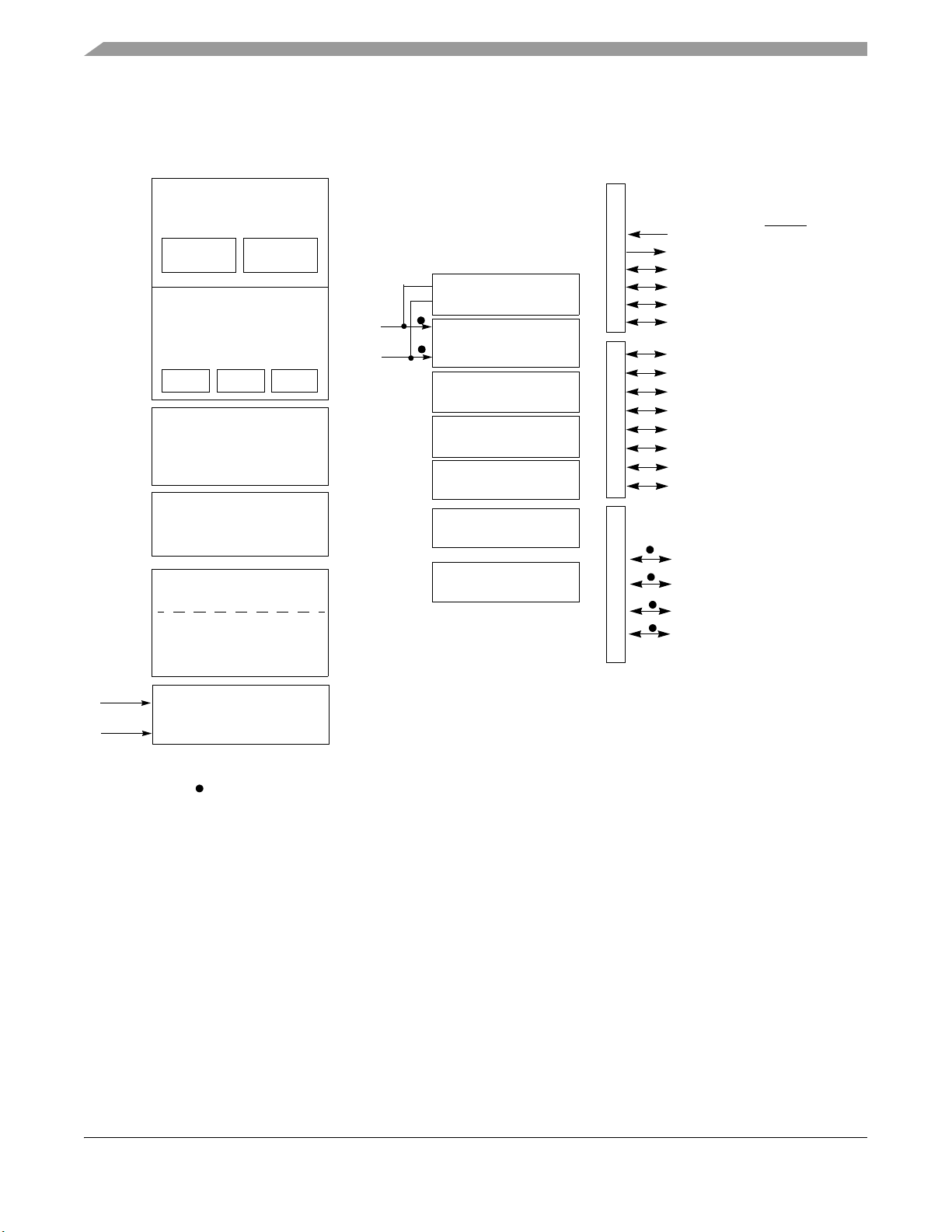
Chapter 1 Device Overview
USER FLASH
USER RAM
HCS08 CORE
CPU
BDC
16-BIT TIMER/PWM
MODULE (TPM)
PTB7/EXTAL
PORT B
HCS08 SYSTEM CONTROL
RESETS AND INTERRUPTS
MODES OF OPERATION
POWER MANAGEMENT
COP
LVD
8-BIT MODULO TIMER
MODULE (MTIM)
PTB6/XTAL
PTB5/TPMCH0
PTB4
PTB3/KBIP7/ADP7
PTB2/KBIP6/ADP6
VOLTAGE REGULATOR
PORT A
PTA1/KBIP1/ADP1/ACMP–
ANALOG COMPARATOR
(ACMP)
LOW-POWER OSCILLATOR
20 MHz INTERNAL CLOCK
SOURCE (ICS)
31.25 kHz to 38.4 kHz
1 MHz to 16 MHz
(XOSC)
V
SS
V
DD
ANALOG-TO-DIGITAL
CONVERTER (ADC)
12-BIT
PTB1/KBIP5/TxD/ADP5
PTB0/KBIP4/RxD/ADP4
PORT C
REAL-TIME COUNTER
(MC9S08QL8 = 8192 BYTES)
(MC9S08QL4 = 4096 BYTES)
(MC9S08QL8 = 512 BYTES)
(MC9S08QL4 = 256 BYTES)
PTA3/KBIP3/ADP3
PTA2/KBIP2/ADP2
PTA0/KBIP0/TPMCH0/ADP0/ACMP
PTA4/ACMPO/BKGD/MS
PTA5/IRQ/TCLK/RESET
IRQ
pins not available on 16-pin package
(RTC)
PTC3
PTC2
PTC1
PTC0
V
REFL/VSSA
V
REFH/VDDA
SERIAL COMMUNICATIONS
INTERFACE MODULE (SCI)
KEYBOARD INTERRUPT
(KBI)
1
V
DDA/VREFH
and V
SSA/VREFL
are double bonded to V
DD
and VSS
1.2 MCU Block Diagram
The block diagram in Figure 1-1 shows the structure of the MC9S08QL8 series MCU.
Figure 1-1. MC9S08QL8 Series Block Diagram
MC9S08QL8 MCU Series Reference Manual, Rev. 1
14 NXP Semiconductors
Page 15
Chapter 1 Device Overview
TPM MTIM
BDCCPU
ADC
3
FLASH
2
ICS
ICSOUT
2
BUSCLK
ICSLCLK
ICSIRCLK
COP
1
The fixed frequency clock (FFCLK) is internally synchronized to the bus clock and
must not exceed one half of the bus clock frequency. It is XCLK in Chapter 12,
Modulo Timer (S08MTIMV1).
2
Flash has frequency requirements for program and erase operation. See
MC9S08QL8 Series Data Sheet for details.
3
ADC has minimum and maximum frequency requirements. See Chapter 10,
Analog-to-Digital Converter (S08ADC12V1) and MC9S08QL8 Data Sheet for
details.
XOSCVLP
EXTAL
XTAL
FFCLK
1
ICSFFCLK
RTC
1 kHZ
LPO
TCLK
ICSERCLK
2
SYNC*
LPOCLK
OSCOUT
SCI
Table 1-2 provides the functional version of the on-chip modules.
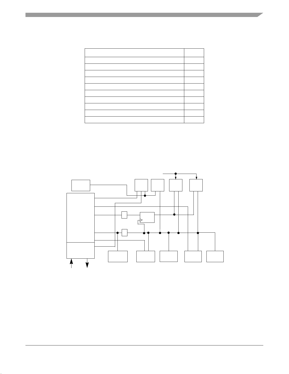
Table 1-2. Module Versions
Module Version
Analog Comparator (ACMPVLP) 1
Analog-to-Digital Converter (ADC12) 1
Central Processor Unit (CPU) 5
Internal Clock Source (ICS) 3
Keyboard Interrupt (KBI) 2
Low Power Oscillator (XOSCVLP) 1
Modulo Timer (MTIM) 1
Real-Time Counter (RTC) 1
Timer Pulse Width Modulator (TPM) 3
Serial Communications Interface (SCI) 4
1.3 System Clock Distribution
Figure 1-2 shows a simplified clock connection diagram. Some modules in the MCU have selectable clock
inputs. The clock inputs to the modules indicate the clock(s) that are used to drive the module functions.
All memory mapped registers associated with the modules are clocked with BUSCLK.
Figure 1-2. System Clock Distribution Diagram
NXP Semiconductors 15
MC9S08QL8 MCU Series Reference Manual, Rev. 1
Page 16

Chapter 1 Device Overview
The ICS supplies the following clock sources:
• ICSOUT — This clock source is used as the CPU clock and is divided by 2 to generate the
peripheral bus clock, BUSCLK. Control bits in the ICS control registers determine which of three
clock sources is connected:
— Internal reference clock
— External reference clock
— Frequency-locked loop (FLL) output
See Chapter 11, Internal Clock Source (S08ICSV3) for details on configuring the ICSOUT clock.
• ICSLCLK — This clock source is derived from the digitally controlled oscillator, DCO, of the ICS
when the ICS is configured to run off of the internal or external reference clock. Development tools
can select this internal self-clocked source (~ 8 MHz) to speed up BDC communications in systems
where the bus clock is slow.
• ICSERCLK — This is the external reference clock and can be selected as the alternate clock for
the ADC module. Section 11.4.7, External Reference Clock explains the ICSERCLK in more
detail. See Chapter 10, Analog-to-Digital Converter (S08ADC12V1) for more information
regarding the use of ICSERCLK with these modules.
• ICSIRCLK — This is the internal reference clock and can be selected as the real-time counter clock
source. Chapter 11, Internal Clock Source (S08ICSV3) explains the ICSIRCLK in more detail. See
Chapter 13, Real-Time Counter (S08RTCV1) for more information regarding the use of
ICSIRCLK.
• ICSFFCLK — This generates the fixed frequency clock (FFCLK) after being synchronized to the
bus clock. It can be selected as clock source for the TPM module and MTIM module. The
frequency of the ICSFFCLK is determined by the settings of the ICS. See Section 11.4.8, Fixed
Frequency Clock in Chapter 11, Internal Clock Source (S08ICSV3) for details.
• LPOCLK — This clock is generated from an internal low power oscillator that is completely
independent of the ICS module. The LPOCLK can be selected as the clock source to the RTC or
COP modules. See Chapter 13, Real-Time Counter (S08RTCV1) and Section 5.4, Computer
Operating Properly (COP) Watchdog for details on using the LPOCLK with these modules.
• OSCOUT — This is the output of the XOSCVLP module and can be selected as the real-time
counter clock source.
• TCLK — TCLK is the optional external clock source for the TPM and MTIM modules. The TCLK
must be limited to 1/4th the frequency of the bus clock for synchronization. See Chapter 15,
Timer/Pulse-Width Modulator (S08TPMV3) and Chapter 12, Modulo Timer (S08MTIMV1) for
more details.
MC9S08QL8 MCU Series Reference Manual, Rev. 1
16 NXP Semiconductors
Page 17

Chapter 2
1
2
3
4
5
6
7
8
9
10
11
13
14
PTC2
PTB4
PTC3
PTC0
PTB3/KBIP7/ADP7
PTB2/KBIP6/ADP6
PTB1/KBIP5/TxD/ADP5
PTB0/KBIP4/RxD/ADP4
PTA2/KBIP2/ADP2
PTA3/KBIP3/ADP3
PTA1/KBIP1/ADP1/ACMP–
PTA0/KBIP0/TPMCH0/ADP0/ACMP+
PTC1
PTA5/IRQ/TCLK/RESET
PTA4/ACMPO/BKGD/MS
V
DD
V
SS
PTB7/EXTAL
PTB6/XTAL
PTB5/TPMCH0
15
16
17
18
19
20
12
Pins shown in bold type are lost in the next lower pin count package.
Pins and Connections
2.1 Introduction
This chapter describes signals that connect to package pins. It includes pinout diagrams, a signal properties
table, and a detailed signal discussion.
2.2 Device Pin Assignment
Figure 2-1 and Figure 2-2 shows the pin assignments in the packages for the MC9S08QL8 series devices.
Figure 2-1. MC9S08QL8 Series in 20-Pin TSSOP Package
MC9S08QL8 MCU Series Reference Manual, Rev. 1
NXP Semiconductors 17
Page 18

Chapter 2 Pins and Connections
1
2
3
4
5
6
7
8
9
10
11
13
14
PTB4
PTB3/KBIP7/ADP7
PTB2/KBIP6/ADP6
PTB1/KBIP5/TxD/ADP5
PTB0/KBIP4/RxD/ADP4
PTA2/KBIP2/ADP2
PTA3/KBIP3/ADP3
PTA1/KBIP1/ADP1/ACMP–
PTA0/KBIP0/TPMCH0/ADP0/ACMP+
PTA5/IRQ/TCLK/RESET
PTA4/ACMPO/BKGD/MS
V
DD
V
SS
PTB7/EXTAL
PTB6/XTAL
PTB5/TPMCH0
15
16
12
Figure 2-2. MC9S08QL8 Series in 16-Pin TSSOP Packages
18 NXP Semiconductors
MC9S08QL8 MCU Series Reference Manual, Rev. 1
Page 19
Chapter 2 Pins and Connections
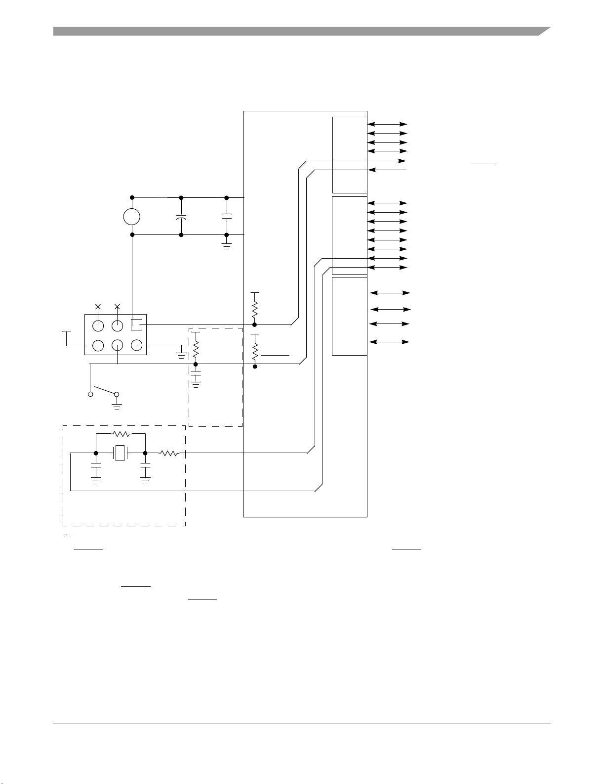
BKGD/MS
RESET/IRQ
OPTIONAL
MANUAL
RESET
PORT
A
V
DD
BACKGROUND HEADER
C2
C1
X1
R
F
R
S
SYSTEM
POWER
PTA0/KBIP0/TPMCH0/ADP0/ACMP+
PTA1/KBIP1/ADP1/ACMP–
PTA2/KBIP2/ADP2
PTA3/KBIP3/ADP3
PTA4/ACMPO/BKGD/MS
PTA5/IRQ/TCLK/RESET
PORT
B
PTB0/KBIP4/RxD/ADP4
PTB1/KBIP5/TxD/ADP5
PTB2/KBIP6/ADP6
PTB3/KBIP7/ADP7
PTB4
PTB5/TPMCH0
PTB6/XTAL
PTB7/EXTAL
PORT
C
MC9S08QL8
V
DDA/VREFH
V
SSA/VREFL
C
BY
0.1 F
C
BLK
10 F
+
+
OPTIONAL EXTERNAL OSCILLATOR
OPTIONAL
EMC
PROTECTION
V
DD
4.7 k–10 k
0.1F
XTAL
EXTAL
NOTES:
1
V
DDA/VREFH
and V
SSA/VREFL
are tired with VDD and VSS respectively.
2
RESET pin can only be used to reset into user mode, you can not enter BDM using RESET pin. BDM can be entered
by holding MS low during POR or writing a 1 to BDFR in SBDFR with MS low after issuing BDM command.
3
When PTA5 is configured as IRQ, pin has optional internal pullup device.
4
RC filter on RESET/IRQ pin is recommended for noisy environments.
5
When PTA5 is configured as RESET, pin becomes bi-directional with output being open-drain drive containing an
internal pullup device.
6
When PTA4 is configured as BKGD, pin becomes bi-directional
7
When using the XOSCVLP module in low range and low power mode, the external components RF, RS, C1 and C2
are not required.
(NOTE 4)
(NOTE 2)
(NOTE 3,5)
(NOTE 6)
(NOTE 7)
3 V
(NOTE 1)
(NOTE 1)
PTC0
PTC1
PTC2
PTC3
2.3 Recommended System Connections
Figure 2-3 shows pin connections that are common to MC9S08QL8 series application systems.
Figure 2-3. Basic System Connections
MC9S08QL8 MCU Series Reference Manual, Rev. 1
NXP Semiconductors 19
Page 20

Chapter 2 Pins and Connections
2.4 Pin Detail
This section provides a detailed description of system connections.
2.4.1 Power Pins
VDD and VSS are the primary power supply pins for the MCU. This voltage source supplies power to all
I/O buffer circuitry and to an internal voltage regulator. The internal voltage regulator provides a regulated
lower-voltage source for the CPU and other internal circuitry of the MCU.
Typically, application systems have two separate capacitors across the power pins. In this case, there must
be a bulk electrolytic capacitor, such as a 10-F tantalum capacitor, to provide bulk charge storage for the
overall system and a 0.1-F ceramic bypass capacitor located as near to the MCU power pins as practical
to suppress high-frequency noise.
V
and V
DDA
ADC and ACMP modules.
are the analog power supply pins for the MCU. This voltage source supplies power to the
SSA
The V
for the ADC module. For this MCU, V
pin. For this MCU, V
REFH
and V
pins are the voltage reference high and voltage reference low inputs, respectively
REFL
shares the V
SSA
shares the V
DDA
pin, and they are double bonded to the VSS pin.
REFL
pin and they are double bonded to the VDD
REFH
2.4.2 Oscillator
Immediately after reset, the MCU uses an internally generated clock provided by the internal clock source
(ICS) module. The oscillator can be configured to run in stop2 or stop3 modes. For more information on
the ICS, see Chapter 11, Internal Clock Source (S08ICSV3).
The oscillator (XOSCVLP) in this MCU is a Pierce oscillator that can accommodate a crystal or ceramic
resonator. An external clock source can optionally be connected to the EXTAL input pin.
Refer to Figure 2-3 for the following discussion. RS (when used) and RF must be low-inductance resistors
such as carbon composition resistors. Wire-wound resistors and some metal film resistors have too much
inductance. C1 and C2 normally must be high-quality ceramic capacitors that are specifically designed for
high-frequency applications.
RF provides a bias path to keep the EXTAL input in its linear range during crystal startup; its value is not
generally critical. Typical systems use 1 M to 10 M. Higher values are sensitive to humidity and lower
values reduce gain and (in extreme cases) could prevent startup.
C1 and C2 are typically in the 5 pF to 25 pF range and are chosen to match the requirements of a specific
crystal or resonator. Be sure to consider printed circuit board (PCB) capacitance and MCU pin capacitance
when selecting C1 and C2. The crystal manufacturer typically specifies a load capacitance which is the
series combination of C1 and C2 (which are usually the same size). As a first-order approximation, use
10 pF as an estimate of combined pin and PCB capacitance for each oscillator pin (EXTAL and XTAL).
When using the oscillator in low range and low gain mode, the external components RS, RF, C1 and C2 are
not required.
MC9S08QL8 MCU Series Reference Manual, Rev. 1
20 NXP Semiconductors
Page 21

Chapter 2 Pins and Connections
2.4.3 RESET Pin
After a power-on reset (POR), the PTA5/IRQ/TCLK/RESET pin defaults to a general-purpose input port
pin, PTA5. Setting RSTPE in SOPT1 configures the pin to be the RESET pin with an open-drain drive
containing an internal pullup device. Once PTA5 is configured as RESET, the pin will function as RESET
until the next POR or LVD reset. When enabled, the RESET
external source when the pin is driven low.
Internal power-on reset and low-voltage reset circuitry typically make external reset circuitry unnecessary.
This pin is normally connected to the standard 6-pin background debug connector so a development
system can directly reset the MCU system. A manual external reset can be added by supplying a simple
switch to ground (pull reset pin low to force a reset).
Whenever any non-POR reset is initiated (whether from an external signal or from an internal system), the
enabled R
ESET pin is driven low for about 34 bus cycles. The reset circuitry decodes the cause of reset
and records it by setting a corresponding bit in the system reset status register (SRS).
NOTE
This pin does not contain a clamp diode to VDD and must not be driven
above VDD.
NOTE
pin can be used to reset the MCU from an
The voltage on the internally pulled up RESET pin when measured will be
below VDD. The internal gates connected to this pin are pulled to VDD. If
the RESET pin is required to drive to a V
level an external pullup must
DD
be used.
NOTE
In EMC-sensitive applications, an external RC filter is recommended on the
RESET pin, if enabled. See Figure 2-3 for an example.
2.4.4 Background / Mode Select (BKGD/MS)
During a power-on-reset (POR) or a background debug force reset (see Section 5.8.3, System Background
Debug Force Reset Register (SBDFR) for more information), the PTA4/ACMPO/BKGD/MS pin
functions as a mode select pin. Immediately after any reset, the pin functions as the background pin and
can be used for background debug communication. When enabled as the BKGD/MS pin (BKGDPE = 1),
an internal pullup device is automatically enabled.
The background debug communication function is enabled when BKGDPE in SOPT1 is set. BKGDPE is
set following any reset of the MCU and must be cleared to use the PTA4/ACMPO/BKGD/MS pin’s
alternative pin functions.
If nothing is connected to this pin, the MCU will enter normal operating mode at the rising edge of the
internal reset after a POR, or force a background debug controller (BDC) reset. If a debug system is
connected to the standard 6-pin background debug header, it can hold BKGD/MS low during a POR or
after issuing a background debug force reset. This will force the MCU into active background mode.
MC9S08QL8 MCU Series Reference Manual, Rev. 1
NXP Semiconductors 21
Page 22

Chapter 2 Pins and Connections
NOTE
A resistive or capacitive load on the PTA4/ACMPO/BKGD/MS pin could
cause the MCU to enter active background mode on a POR if the pin voltage
rises slower than VDD.
The BKGD/MS pin is used primarily with BDC communications, and features a custom protocol that uses
16 clock cycles of the target MCU’s BDC clock per bit time. The target MCU’s BDC clock can run as fast
as the bus clock, so no significant capacitance must be connected to the BKGD/MS pin that could interfere
with background serial communications.
Although the BKGD/MS pin is a pseudo open-drain pin, the background debug communication protocol
provides brief, actively driven, high speedup pulses to ensure fast rise times. Small capacitances from
cables and the absolute value of the internal pullup device play a minimal role in determining rise and fall
times on the BKGD/MS pin.
2.4.5 General-Purpose I/O (GPIO) and Peripheral Ports
The MC9S08QL8 series of MCUs support up to 16 general-purpose I/O pins, 1 input-only pin, and 1
output-only pin, which are shared with on-chip peripheral functions (timer, ADC, ACMP, etc.). The GPIO
output-only (PTA4/ACMPO/BKGD/MS) and input-only (PTA5/IRQ/TCLK/RESET) pins are
bi-directional when configured as BKGD and RESET, respectively.
When a port pin is configured as a general-purpose output or a peripheral uses the port pin as an output,
software can select one of two drive strengths and enable or disable slew rate control. When a port pin is
configured as a general-purpose input or a peripheral uses the port pin as an input, software can enable a
pullup device.
PTA5 is a special I/O pin. When the PTA5/IRQ/TCLK/RESET pin is configured as PTA5 input with the
pullup enabled, the voltage observed on the pin will not be pulled to VDD. However, the internal voltage
on the PTA5 node will be at VDD.
When an on-chip peripheral system is controlling a pin, data direction control bits still determine what is
read from port data registers even though the peripheral module controls the pin direction by controlling
the enable for the pin’s output buffer. For information about controlling these pins as general-purpose I/O
pins, see Chapter 6, Parallel Input/Output Control.
NOTE
To avoid extra current drain from floating input pins, the reset initialization
routine in the application program must enable on-chip pullup devices or
change the direction of unused or non-bonded pins to outputs so they do not
float.
When using the 16-pin device, the user must either enable on-chip pullup
devices or change the direction of non-bonded PTC3–PTC0 pins to outputs
so the pins do not float.
MC9S08QL8 MCU Series Reference Manual, Rev. 1
22 NXP Semiconductors
Page 23

Table 2-1. Pin Availability by Package Pin-Count
Chapter 2 Pins and Connections
Pin
Number
<-- Lowest Priority --> Highest
20 16 Port Pin Alt 1 Alt 2 Alt 3 Alt 4
1 1 PTA5 IRQ TCLK RESET
—
2 2 PTA4 ACMPO BKGD MS —
33—— ——V
44—— ——V
DD
SS
5 5 PTB7 — — — EXTAL
6 6 PTB6 — — — XTAL
1
7 7 PTB5 TPMCH0
———
8 8 PTB4 — — — —
9—PTC3— ———
10—PTC2— ———
11—PTC1— ———
12—PTC0— ———
13 9 PTB3 KBIP7 — ADP7 —
14 10 PTB2 KBIP6 — ADP6 —
15 11 PTB1 KBIP5 TxD ADP5 —
16 12 PTB0 KBIP4 RxD ADP4 —
17 13 PTA3 KBIP3 — ADP3 —
18 14 PTA2 KBIP2 — ADP2 —
2
19 15 PTA1 KBIP1 — ADP1
20 16 PTA0 KBIP0 TPMCH0 ADP0
1
TPMCH0 pin can be repositioned at PTB5 using TPMCH0PS in SOPT2,
ACMP–
2
ACMP+
default reset location is PTA0.
2
If ADC and ACMP are enabled, both modules will have access to the pin.
2
2
MC9S08QL8 MCU Series Reference Manual, Rev. 1
NXP Semiconductors 23
Page 24

Chapter 2 Pins and Connections
MC9S08QL8 MCU Series Reference Manual, Rev. 1
24 NXP Semiconductors
Page 25

Chapter 3 Modes of Operation
3.1 Introduction
The operating modes of the MC9S08QL8 series are described in this chapter. Entry into each mode, exit
from each mode, and functionality while in each of the modes are described.
3.2 Features
• Active background mode for code development
• Run mode — CPU clocks can be run at full speed and the internal supply is fully regulated.
• LPRUN mode — CPU and peripheral clocks are restricted to 125 kHz at maximum and the internal
voltage regulator is in standby
• Wait mode — CPU shuts down to conserve power; system clocks are running and full regulation
is maintained
• LPWAIT mode — CPU shuts down to conserve power; peripheral clocks are restricted to 125 kHz
in maximum and the internal voltage regulator is in standby
• Stop modes — System clocks are stopped and voltage regulator is in standby
— Stop3 — All internal circuits are powered for fast recovery
— Stop2 — Partial power down of internal circuits, RAM content is retained, I/O states held
3.3 Run Mode
This is the normal operating mode for the MC9S08QL8 series. In this mode, the CPU executes code from
internal memory with execution beginning at the address fetched from memory at 0xFFFE–0xFFFF after
reset.
3.3.1 Low Power Run Mode (LPRun)
In the low power run mode, the on-chip voltage regulator is put into its standby state. This state uses the
minimum power consumption necessary for CPU functionality. Power consumption is most reduced by
disabling the clocks to all unused peripherals by clearing the corresponding bits in the SCGC1 and SCGC2
registers.
Before entering this mode, the following conditions must be met:
• FBELP is the selected clock mode for the ICS.
• The HGO bit in the ICSC2 register is clear.
• The bus frequency is less than 125 kHz.
MC9S08QL8 MCU Series Reference Manual, Rev. 1
NXP Semiconductors 25
Page 26

Chapter 3 Modes of Operation
• If enabled, the ADC must be configured to use the asynchronous clock source, ADACK, to meet
the ADC minimum frequency requirements. The bandgap channel cannot be converted in low
power run mode.
• The LVD and LVW must be disabled by clearing either the LVDE or LVDSE bits in the SPMSC1
register.
• Flash programming/erasing is not allowed.
• ACMP option to compare to internal bandgap reference is not allowed in LPRUN and LPWAIT.
Once these conditions are met, low power run mode can be entered by setting the LPR bit in the SPMSC2
register.
To re-enter standard run mode, clear the LPR bit. The LPRS bit in the SPMSC2 register is a read-only
status bit that can be used to determine if the regulator is in full regulation mode or not. When LPRS is ‘0’,
the regulator is in full regulation mode and the MCU can run at full speed in any clock mode.
3.3.1.1 Interrupts in Low Power Run Mode
Low power run mode provides the option to return to full regulation if any interrupt occurs. This is done
by setting the LPWUI bit in the SPMSC2 register. The ICS can then be set for full speed immediately in
the interrupt service routine.
If the LPWUI bit is clear, interrupts will be serviced in low power run mode.
If the LPWUI bit is set, LPR and LPRS bits will be cleared and interrupts will be serviced with the
regulator in full regulation.
3.3.1.2 Resets in Low Power Run Mode
Any reset will exit low power run mode, clear the LPR and LPRS bits, and return the device to normal run
mode.
3.4 Active Background Mode
The active background mode functions are managed through the BDC in the HCS08 core. The BDC
provides the means for analyzing MCU operation during software development.
Active background mode is entered in any of five ways:
• When the BKGD/MS pin is low during POR
• When the BKGD/MS pin is low immediately after issuing a background debug force reset (see
Section 5.8.3, System Background Debug Force Reset Register (SBDFR)).
• When a BACKGROUND command is received through the BKGD/MS pin
• When a BGND instruction is executed
• When encountering a BDC breakpoint
After entering active background mode, the CPU is held in a suspended state while it waits for serial
background commands instead of executing instructions from the user application program.
Background commands are of two types:
MC9S08QL8 MCU Series Reference Manual, Rev. 1
26 NXP Semiconductors
Page 27

Chapter 3 Modes of Operation
• Non-intrusive commands, defined as commands that can be issued while the user program is
running. Non-intrusive commands can be issued through the BKGD pin while the MCU is in run
mode; non-intrusive commands can also be executed when the MCU is in the active background
mode. Non-intrusive commands include:
— Memory access commands
— Memory-access-with-status commands
— BDC register access commands
— The BACKGROUND command
• Active background commands, which can only be executed while the MCU is in active background
mode. Active background commands include commands to:
— Read or write CPU registers
— Trace one user program instruction at a time
— Leave active background mode to return to the user application program (GO)
The active background mode is used to program a bootloader or user application program into the flash
program memory before the MCU is operated in run mode for the first time. When the MC9S08QL8 series
are shipped from the NXP Semiconductors factory, the flash program memory is erased by default unless
specifically noted. As a result, no program can be executed in run mode until the flash memory is initially
programmed. The active background mode can also be used to erase and reprogram the flash memory after
it has been previously programmed.
For additional information about the active background mode, refer to the Chapter 16, Development
Support.
3.5 Wait Mode
Wait mode is entered by executing a WAIT instruction. Upon execution of the WAIT instruction, the CPU
enters a low-power state in which it is not clocked. The I bit in CCR is cleared when the CPU enters the
wait mode, enabling interrupts. When an interrupt request occurs, the CPU exits the wait mode and
resumes processing, beginning with the stacking operations that lead to the interrupt service routine.
While the MCU is in wait mode, there are some restrictions on which background debug commands can
be used. Only the BACKGROUND command and memory-access-with-status commands are available
when the MCU is in wait mode. The memory-access-with-status commands do not allow memory access,
but they report an error indicating that the MCU is in either stop or wait mode. The BACKGROUND
command can be used to wake the MCU from wait mode and enter active background mode.
3.5.1 Low Power Wait Mode (LPWait)
Low power wait mode is entered by executing a WAIT instruction while the MCU is in low power run
mode. In the low power wait mode, the on-chip voltage regulator remains in its standby state (as in the low
power run mode). This state uses the minimum power consumption necessary for most modules to
maintain functionality. Power consumption is most reduced by disabling the clocks to all unused
peripherals by clearing the corresponding bits in the SCGC register.
The same restrictions on the low power run mode apply to low power wait mode.
MC9S08QL8 MCU Series Reference Manual, Rev. 1
NXP Semiconductors 27
Page 28

Chapter 3 Modes of Operation
3.5.1.1 Interrupts in Low Power Wait Mode
If the LPWUI bit is set when the WAIT instruction is executed, then the voltage regulator will return to
full regulation when wait mode is exited. The ICS can be set for full speed immediately in the interrupt
service routine.
If the LPWUI bit is clear when the WAIT instruction is executed, an interrupt will return the device to low
power run mode.
If the LPWUI bit is set when the WAIT instruction is executed, an interrupt will return the device to normal
run mode with full regulation and the LPR and LPRS bits will be cleared.
3.5.1.2 Resets in Low Power Wait Mode
Any reset will exit low power wait mode, clear the LPR and LPRS bits, and return the device to normal
run mode.
3.6 Stop Modes
One of two stop modes (stop2 or stop3) is entered upon execution of a STOP instruction when the STOPE
bit in the system option 1 register (SOPT1) is set. In both stop modes, the bus and CPU clocks are halted.
In stop3 the voltage regulator is in standby. In stop2 the voltage regulator is in partial powerdown. The ICS
module can be configured to leave the reference clocks running. See Chapter 11, Internal Clock Source
(S08ICSV3) for more information.
If the STOPE bit is not set when the CPU executes a STOP instruction, the MCU will not enter either stop
mode and an illegal opcode reset is forced. The stop modes are selected by setting the appropriate bits in
the System Power Management Status and Control 2 Register (SPMSC2).
Table 3-1 shows all of the control bits that affect stop mode selection and the mode selected under various
conditions. The selected mode is entered following the execution of a STOP instruction.
Table 3-1. Stop Mode Selection
Register SOPT1 BDCSCR SPMSC1 SPMSC2
1
Bit name STOPE ENBDM
0 x x x Stop modes disabled; illegal opcode reset if STOP
1 1 x x Stop3 with BDM enabled
1 0 Both bits must be 1 x Stop3 with voltage regulator active
1 0 Either bit a 0 0 Stop3
1 0 Either bit a 0 1 Stop2
1
ENBDM is located in the BDCSCR which is accessible only through BDC commands, see Chapter 16, Development
Support.
2
When in stop3 mode with BDM enabled, The S
LVD E LVD SE PP DC
will be near R
IDD
instruction executed
levels because internal clocks are enabled.
IDD
Stop Mode
2
MC9S08QL8 MCU Series Reference Manual, Rev. 1
28 NXP Semiconductors
Page 29

Chapter 3 Modes of Operation
3.6.1 Stop2 Mode
Stop2 mode is entered by executing a STOP instruction under the conditions as shown in Tabl e 3-1. Most
of the internal circuitry of the MCU is powered off in stop2 with the exception of the RAM and optionally
the RTC and low power oscillator. Upon entering stop2, all I/O pin control signals are latched so that the
pins retain their states during stop2.
Exit from stop2 is performed by asserting the wakeup pin (PTA5/IRQ/TCLK/RESET) on the MCU.
NOTE
PTA5/IRQ/TCLK/RESET is an active low wakeup. To avoid an immediate
exit from stop 2, either the internal pullup must be enabled prior to
executing a STOP instruction or an external pullup must be connected. If
PTA5/IRQ/TCLK/RESET is not to be used as the wakeup pin, configure it
as PTA5 with the pullup enabled.
In addition, the real-time counter (RTC) can wake the MCU from stop2, if enabled.
Upon wakeup from stop2 mode, the MCU starts up as from a power-on reset (POR):
• All module control and status registers are reset, except for SPMSC1-SPMSC3, RTCSC, RTCCNT
and RTCMOD.
• The LVD reset function is enabled and the MCU remains in the reset state if V
trip point
is below the LVD
DD
• The CPU takes the reset vector
In addition to the above, upon waking from stop2, the PPDF bit in SPMSC2 is set. This flag is used to
direct user code to go to a stop2 recovery routine. PPDF remains set and the I/O pin states remain latched
until a 1 is written to PPDACK in SPMSC2.
If using the low power oscillator during stop2, the user must reconfigure the ICSC2 register which contains
oscillator control bits before PPDACK is written.
To maintain I/O states for pins that were configured as GPIO before entering stop2, the user must restore
the contents of the I/O port registers, which have been saved in RAM, to the port registers before writing
to the PPDACK bit. If the port registers are not restored from RAM before writing to PPDACK, then the
pins will switch to their reset states when PPDACK is written.
For pins that were configured as peripheral I/O, the user must reconfigure the peripheral module that
interfaces to the pin before writing to the PPDACK bit. If the peripheral module is not enabled before
writing to PPDACK, the pins will be controlled by their associated port control registers when the I/O
latches are opened.
3.6.1.1 Stop2 Mode Recovery Time
The stop2 recovery time is defined as the interval from the exit trigger to the first opcode fetch. There are
three main components to this wakeup time: the voltage regulator recovery time, the clock source start up
time, and the reset processing time.
MC9S08QL8 MCU Series Reference Manual, Rev. 1
NXP Semiconductors 29
Page 30

Chapter 3 Modes of Operation
The voltage regulator recovery time (t
) is provided in the data sheet. This time is not influenced by the
VRR
clock source frequency or VDD and is therefore relatively consistent.
Since exiting from stop2 causes the MCU to wake as if a POR occurred, the standard reset processing will
always occur which takes about 150 ICSOUT cycles after the clock source has started. Therefore, the
equation for stop2 recovery time is
Stop2 recovery time = t
+ clock start up time + 150 ICSOUT cycles. Eqn. 3-1
VRR
Since ICSOUT defaults to FLL output running at 8.4 MHz during a reset, and the FLL takes about 1 ms
to start outputting a clock signal (although it won’t be stable initially) Equation 3-5 simplifies to
Stop2 recovery time = t
+ 1 sec + 17.9 s. Eqn. 3-2
VRR
3.6.2 Stop3 Mode
Stop3 mode is entered by executing a STOP instruction under the conditions shown in Table 3-1. The
states of all of the internal registers and logic, RAM contents, and I/O pin states are maintained.
Stop3 can be exited by asserting RESET, or by an interrupt from one of the following sources: the RTC,
LVD, LVW, ADC, ACMP, IRQ, SCI or the KBI.
If stop3 is exited by means of the RESET pin, then the MCU is reset and operation will resume after taking
the reset vector. Exit by means of one of the internal interrupt sources results in the MCU taking the
appropriate interrupt vector.
3.6.2.1 Stop3 Mode Recovery Time
The stop3 recovery time is defined as the interval from the exit trigger to the first opcode fetch. There are
three main components to this wakeup time: the voltage regulator recovery time, the clock source start up
time, and the reset or interrupt processing time.
The voltage regulator recovery time (t
clock source frequency or VDD and is therefore relatively consistent.
When an interrupt is used as the exit trigger, the clock must restart and ICSOUT must oscillate six times
before the interrupt processing begins. The interrupt processing requires 11 bus cycles (22 ICSOUT
cycles) for the stacking and vector fetch. Therefore, the first opcode of the interrupt service routine (ISR)
will begin after
Stop3 recovery time = t
The clock source start up time is dependent on the clock mode selected when the MCU enters stop mode.
When the FLL output is selected as the clock source, the FLL starts up within a microsecond at roughly
the same frequency as before stop mode is entered. Typical start up time for the internal reference is given
in the data sheet. Typical start up times for the crystal oscillator are also given in the data sheet.
Assuming the FLL is the selected clock source upon entering stop3 and the FLL is configured for a
20 MHz ICSOUT frequency, then Equation 3-6 simplifies to
) is provided in the data sheet. This time is not influenced by the
VRR
+ clock start up time + 28 ICSOUT cycles. Eqn. 3-3
VRR
MC9S08QL8 MCU Series Reference Manual, Rev. 1
30 NXP Semiconductors
Page 31

Chapter 3 Modes of Operation
Stop3 recovery time = t
+ 1 sec + 1.4 sec Eqn. 3-4
VRR
When reset is used as the exit trigger, more time is required for the reset processing, so Equation 3-3
becomes
Stop3 recovery time = t
+ clock start up time + 162 ICSOUT cycles. Eqn. 3-5
VRR
Since ICSOUT defaults to FLL output running at 8.4 MHz during a reset, Equation 3-5 simplifies to
Stop3 recovery time = t
+ 1 sec + 19.3 sec. Eqn. 3-6
VRR
3.6.3 Active BDM Enabled in Stop Mode
Entry into the active background mode from run mode is enabled if the ENBDM bit in BDCSCR is set.
This register is described in Chapter 16, Development Support. If ENBDM is set when the CPU executes
a STOP instruction, the system clocks to the background debug logic remain active when the MCU enters
stop mode. Because of this, background debug communication remains possible. In addition, the voltage
regulator does not enter its low-power standby state but maintains full internal regulation. If the user
attempts to enter stop2 with ENBDM set, the MCU will instead enter stop3.
Most background commands are not available in stop mode. The memory-access-with-status commands
do not allow memory access, but they report an error indicating that the MCU is in either stop or wait
mode. The BACKGROUND command can be used to wake the MCU from stop and enter active
background mode if the ENBDM bit is set. After entering background debug mode, all background
commands are available.
3.6.4 LVD Enabled in Stop Mode
The LVD system is capable of generating either an interrupt or a reset when the supply voltage drops below
the LVD voltage. If the LVD is enabled in stop (LVDE and LVDSE bits in SPMSC1 both set) the voltage
regulator remains active during stop mode. If the user attempts to enter stop2 with the LVD enabled for
stop, the MCU will instead enter stop3.
3.6.5 Stop Modes in Low Power Run Mode
Stop2 mode cannot be entered from low power run mode. If the PPDC bit is set, then the LPR bit cannot
be set. Likewise, if the LPR bit is set, the PPDC bit cannot be set.
Stop3 mode can be entered from low power run mode by executing the STOP instruction while in low
power run. Exiting stop3 with a reset will put the device back into normal run mode. If LPWUI is clear,
interrupts will exit stop3 mode, return the device to low power run mode, and then service the interrupt. If
LPWUI is set, interrupts will exit stop3 mode, put the device into normal run mode, clear LPR and LPRS
bits, and then service the interrupt.
3.7 Mode Selection
Several control signals are used to determine the current operating mode of the device. Table 3-2 shows
the conditions for each of the device’s operating modes.
MC9S08QL8 MCU Series Reference Manual, Rev. 1
NXP Semiconductors 31
Page 32

Table 3-2. Power Mode Selections
BDCSCR
BDM
Mode of Operation
ENBDM
SPMSC1
PMC
SPMSC2
PMC
CPU & Periph CLKs
1
LVDE LVDSE LPR PPDC BDM Clock
RUN mode 0 x x 0 x on. ICS in any mode. off on
11 1
1xxx on
LPRUN mode 0 0 x 1 0 low freq required. ICS in
MC9S08QL8 MCU Series Reference Manual, Rev. 1
10
FBELP mode only.
WAIT mode - (Assumes WAIT instruction executed.) 0 x x 0 x CPU clock is off;
11 1
1xxx on
peripheral clocks on. ICS
state same as RUN mode.
LPWAIT mode - (Assumes WAIT instruction executed.) 0 0 x 1 0 CPU clock is off;
peripheral clocks
at low speed. ICS in
ICSIRCLK, and OSCOUT
STOP3 - (Assumes STOPE bit is set and STOP
instruction executed.) Note that STOP3 is used in
place of STOP2 if the BDM or LVD is enabled.
10
0 0 x x 0 ICS in STOP. ICSERCLK
010x0 off
0 1 1 x x off on - stop
1 x x x x ICSLCLK still active. on
STOP2 - (Assumes STOPE bit is set and STOP
instruction executed.) If BDM or LVD is enabled,
STOP3 will be invoked rather than STOP2.
1
ENBDM is located in the BDC status and control register (BDCSCR) which is write accessible only through BDC commands.
2
Configured within the ICS module based on the settings of IREFSTEN, EFRESTEN, IRCLKEN and ERCLKEN.
3
In stop2, CPU, Flash, ICS and all peripheral modules are powered down except for the RTC.
0 0 x 0 1 OSCOUT optionally on
10
FBELP mode.
optionally on
Affects on Sub-System
Voltage
Regulator
off standby
off on
off standby
off standby
2
currents
will be
increased
2,3
off partial
powerdown
Page 33

Chapter 3 Modes of Operation
Mode Regulator State
RUN Full on
WAIT Full on
LPRUN Standby
LPWAIT Standby
STOP3 Standby
STOP2 Partial powerdown
STOP3
1
STOP2
LPWAITWAIT
RUN LPRUN
47
6
2
53
Figure 3-1. Allowable Power Mode Transitions for the MC9S08QL8 Series
Figure 3-1 illustrates mode state transitions allowed between the legal states shown in Table 3-1.
PTA5/IRQ/TCLK/RESET must be asserted low in order to exit stop2. Interrupts suffice for the other stop
and wait modes.
Table 3-3 defines triggers for the various state transitions shown in Figure 3-1.
Table 3-3. Triggers for Transitions Shown in Figure 3-1
Transition # From To Trigger
1 RUN LPRUN Configure settings shown in Ta ble 3 -1 , switch LPR=1 last
LPRUN RUN Clear LPR
Interrupt when LPWUI=1
2 RUN STOP2 Pre-configure settings shown in Table 3-1, issue STOP
instruction
1
STOP2 RUN assert zero on PTA5/IRQ/TCLK/RESET
environment from RAM
3 LPRUN LPWAIT WAIT instruction
LPWAIT LPRUN Interrupt when LPWUI=0
4 LPRUN STOP3 STOP instruction
STOP3 LPRUN Interrupt when LPWUI=0
5 LPWAIT RUN Interrupt when LPWUI=1
RUN LPWAIT Not supported
6 RUN WAIT WAIT instruction
NXP Semiconductors 33
WAIT RUN Interrupt or reset
MC9S08QL8 MCU Series Reference Manual, Rev. 1
, reload
Page 34

Chapter 3 Modes of Operation
Table 3-3. Triggers for Transitions Shown in Figure 3-1 (continued)
Transition # From To Trigger
7 STOP3 RUN Interrupt (if LPR = 0, or LPR = 1 and LPWUI =1) or reset
RUN STOP3 STOP instruction
1
An analog connection from this pin to the on-chip regulator will wake the regulator, which will then initiate
a power-on-reset sequence.
3.7.1 On-Chip Peripheral Modules in Stop and Low Power Modes
When the MCU enters any stop mode, system clocks to the internal peripheral modules are stopped. Even
in the exception case (ENBDM = 1), where clocks to the background debug logic continue to operate,
clocks to the peripheral systems are halted to reduce power consumption. Refer to Section 3.6.1, Stop2
Mode and Section 3.6.2, Stop3 Mode for specific information on system behavior in stop modes.
When the MCU enters LPWait or LPRun modes, system clocks to the internal peripheral modules continue
based on the settings of the clock gating control registers (SCGC1 and SCGC2).
Table 3-4. Stop and Low Power Mode Behavior
Peripheral
Mode
Stop2 Stop3 LPWait LPRun
CPU Off Standby Standby On
RAM Standby Standby Standby On
Flash Off Standby Standby On
Port I/O Registers Off Standby Standby On
ADC Off Optionally On
ACMP Off Optionally On
BDM Off
3
Optionally On Off
1
2
Optionally On
Optionally On Optionally On
1
4
Optionally On
4
Off
COP Off Off Optionally On Optionally On
ICS Off Optionally On
5
On
6
On
6
IRQ Off Optionally On Optionally On Optionally On
KBI Off Optionally On Optionally On Optionally On
LVD /LVW Off
7
Optionally On Off
8
Off
8
RTC Optionally On Optionally On Optionally On Optionally On
MTIM Off Standby Optionally On Optionally On
SCI Off Standby Optionally On Optionally On
TPM Off Standby Optionally On Optionally On
Voltage Regulator Partial Powerdown Optionally On
XOSCVLP Optionally On
10
Optionally On
9
10
Standby Standby
Optionally On Optionally On
I/O Pins States Held Peripheral Control Peripheral Control On
1
Requires the asynchronous ADC clock. For stop3, LVD must be enabled to run in stop if converting the bandgap channel.
The bandgap channel cannot be converted in LPRun or LPWait.
2
LVD must be enabled to run in stop if using the bandgap as a reference.
1
MC9S08QL8 MCU Series Reference Manual, Rev. 1
34 NXP Semiconductors
Page 35

Chapter 3 Modes of Operation
3
If ENBDM is set when entering stop2, the MCU will actually enter stop3.
4
If ENBDM is set when entering LPRun or LPWait, the MCU will actually stay in run mode or enter wait mode, respectively.
5
IRCLKEN and IREFSTEN set in ICSC1, else in standby.
6
ICS must be configured for FBELP, bus frequency limited to 125 kHz in LPRUN or LPWAIT.
7
If LVDSE is set when entering stop2, the MCU will actually enter stop3.
8
If LVDSE is set when entering LPRun or LPWait, the MCU will actually enter run or wait mode, respectively.
9
Requires the LVD to be enabled, else in standby. See Section 3.6.4, LVD Enabled in Stop Mode.
10
ERCLKEN and EREFSTEN set in ICSC2, else in standby.
MC9S08QL8 MCU Series Reference Manual, Rev. 1
NXP Semiconductors 35
Page 36

Chapter 3 Modes of Operation
MC9S08QL8 MCU Series Reference Manual, Rev. 1
36 NXP Semiconductors
Page 37

Chapter 4
DIRECT PAGE
RAM
512 BYTES
0x0000
0x005F
0x0060
0x1800
0x025F
0x184F
96 BYTES
HIGH
80 BYTES
FLASH
8192 BYTES
5536 BYTES
REGISTERS
PAGE REGISTERS
UNIMPLEMENTED
Address
0xFFFF
0x17FF
0xE000
0x0260
0xDFFF
51120 BYTES
UNIMPLEMENTED
0x1850
MC9S08QL8
DIRECT PAGE
RAM
256 BYTES
0x0000
0x005F
0x0060
0x1800
0x015F
0x184F
96 BYTES
HIGH
80 BYTES
FLASH
4096 BYTES
5792 BYTES
REGISTERS
PAGE REGISTERS
UNIMPLEMENTED
Address
0xFFFF
0x17FF
0xF000
0x0160
0xEFFF
55216 BYTES
UNIMPLEMENTED
0x1850
MC9S08QL4
Memory
4.1 MC9S08QL8 Series Memory Map
As shown in Figure 4-1, on-chip memory in the MC9S08QL8 series of MCUs consists of RAM, flash
program memory for nonvolatile data storage, and I/O and control/status registers. The registers are
divided into three groups:
• Direct-page registers (0x0000 through 0x005F)
• High-page registers (0x1800 through 0x184F)
• Nonvolatile registers (0xFFB0 through 0xFFBF)
4.2 Reset and Interrupt Vector Assignments
Table 4-1 shows address assignments for reset and interrupt vectors. The vector names shown in this table
are the labels used in the NXP Semiconductors provided equate file for the MC9S08QL8 series.
NXP Semiconductors 37
Figure 4-1. MC9S08QL8 Series Memory Maps
MC9S08QL8 MCU Series Reference Manual, Rev. 1
Page 38

Chapter 4 Memory
Table 4-1. Reset and Interrupt Vectors
Address
(High/Low)
0xFFC0:FFC1
Vector Vector Name
Unused Vector Space
(available for user program)
0xFFCC:0xFFCD
0xFFCE:0xFFCF RTC Vrtc
0xFFD0:0xFFD1 Reserved —
0xFFD2:0xFFD3 Reserved —
0xFFD4:0xFFD5 Reserved —
0xFFD6:0xFFD7 ACMP Vacmp
0xFFD8:0xFFD9 ADC Conversion Vadc
0xFFDA:0xFFDB KBI Interrupt Vkeyboard
0xFFDC:0xFFDD Reserved —
0xFFDE:0xFFDF SCI Transmit Vscitx
0xFFE0:0xFFE1 SCI Receive Vscirx
0xFFE2:0xFFE3 SCI Error Vscierr
0xFFE4:0xFFE5 Reserved —
0xFFE6:0xFFE7 MTIM Overflow Vmtim
0xFFE8:0xFFE9 Reserved —
0xFFEA:0xFFEB Reserved —
0xFFEC:0xFFED Reserved —
0xFFEE:0xFFEF Reserved —
0xFFF0:0xFFF1 TPM Overflow Vtpmovf
0xFFF2:0xFFF3 Reserved —
0xFFF4:0xFFF5 Reserved —
0xFFF6:0xFFF7 TPM Channel 0 Vtpmch0
0xFFF8:0xFFF9 Low Voltage Detect or Low Voltage Warning Vlvd
0xFFFA:0xFFFB IRQ Virq
0xFFFC:0xFFFD SWI Vswi
0xFFFE:0xFFFF Reset Vreset
MC9S08QL8 MCU Series Reference Manual, Rev. 1
38 NXP Semiconductors
Page 39

Chapter 4 Memory
4.3 Register Addresses and Bit Assignments
The registers in the MC9S08QL8 series are divided into these groups:
• Direct-page registers are the ones located in the first 96 locations in the memory map; these are
accessible with efficient direct addressing mode instructions.
• High-page registers are used much less often, so they are located above 0x1800 in the memory
map. This leaves more room in the direct page for more frequently used registers and RAM.
• The nonvolatile register area consists of a block of 16 locations in flash memory at 0xFFB0–
0xFFBF. Nonvolatile register locations include:
— NVPROT and NVOPT are loaded into working registers at reset
— An 8-byte backdoor comparison key that optionally allows a user to gain controlled access to
secure memory
Because the nonvolatile register locations are flash memory, they must be erased and programmed
like other flash memory locations.
Direct-page registers can be accessed with efficient direct addressing mode instructions. Bit manipulation
instructions can be used to access any bit in any direct-page register. Table 4-2 is a summary of all
user-accessible direct-page registers and control bits.
The direct-page registers in Tab le 4 -2 can use the more efficient direct addressing mode, which requires
only the lower byte of the address. Because of this, the lower byte of the address in column one is shown
in bold text. In Table 4-3 and Tabl e 4-4, the whole address in column one is shown in bold. In Table 4-2,
Table 4-3, and Tabl e 4-4 , the register names in column two are shown in bold to set them apart from the
bit names to the right. Cells that are not associated with named bits are shaded. A shaded cell with a 0
indicates this unused bit always reads as a 0. Shaded cells with dashes indicate unused or reserved bit
locations that could read as 1s or 0s. When writing to these bits, write a 0 unless otherwise specified.
MC9S08QL8 MCU Series Reference Manual, Rev. 1
NXP Semiconductors 39
Page 40

Chapter 4 Memory
Table 4-2. Direct-Page Register Summary (Sheet 1 of 2)
Address
Register
Name
0x0000 PTAD
0x0001 PTADD
0x0002 PTBD
0x0003 PTBDD
0x0004 PTCD
0x0005 PTCDD
0x0006
–
Reserved
0x000B
0x000C KBISC
0x000D KBIPE
0x000E KBIES
0x000F IRQSC
0x0010 ADCSC1
0x0011 ADCSC2
0x0012 ADCRH
0x0013 ADCRL
0x0014 ADCCVH
0x0015 ADCCVL
0x0016 ADCCFG
0x0017 APCTL1
0x0018
Reserved
–
0x0019
0x001A ACMPSC
0x001B
–
Reserved
0x001F
0x0020 SCIBDH
0x0021 SCIBDL
0x0022 SCIC1
0x0023 SCIC2
0x0024 SCIS1
0x0025 SCIS2
0x0026 SCIC3
0x0027 SCID
0x0028
–
Reserved
0x0037
0x0038 ICSC1
Bit 7654321Bit 0
0 0 PTAD5 PTAD4 PTAD3 PTAD2 PTAD1 PTAD0
0 0 0 0 PTADD3 PTADD2 PTADD1 PTADD0
PTBD7 PTBD6 PTBD5 PTBD4 PTBD3 PTBD2 PTBD1 PTBD0
PTBDD7 PTBDD6 PTBDD5 PTBDD4 PTBDD3 PTBDD2 PTBDD1 PTBDD0
0 0 0 0 PTCD3 PTCD2 PTCD1 PTCD0
0 0 0 0 PTCDD3 PTCDD2 PTCDD1 PTCDD0
—
—
0 0 0 0 KBF KBACK KBIE KBIMOD
KBIPE7 KBIPE6 KBIPE5 KBIPE4 KBIPE3 KBIPE2 KBIPE1 KBIPE0
KBEDG7 KBEDG6 KBEDG5 KBEDG4 KB1EDG3 KB1EDG2 KB1EDG1 KB1EDG0
0 IRQPDD IRQEDG IRQPE IRQF IRQACK IRQIE IRQMOD
COCO AIEN ADCO ADCH
ADACT ADTRG ACFE ACFGT 0 0 R R
0 0 0 0 ADR11 ADR10 ADR9 ADR8
ADR7 ADR6 ADR5 ADR4 ADR3 ADR2 ADR1 ADR0
0 0 0 0 ADCV11 ADCV10 ADCV9 ADCV8
ADCV7 ADCV6 ADCV5 ADCV4 ADCV3 ADCV2 ADCV1 ADCV0
ADLPC ADIV ADLSMP MODE ADICLK
ADPC7 ADPC6 ADPC5 ADPC4 ADPC3 ADPC2 ADPC1 ADPC0
—
—
ACME ACBGS ACF ACIE ACO ACOPE ACMOD1 ACMOD0
—
—
LBKDIE RXEDGIE 0 SBR12 SBR11 SBR10 SBR9 SBR8
SBR7 SBR6 SBR5 SBR4 SBR3 SBR2 SBR1 SBR0
LOOPS SCISWAI RSRC M WAKE ILT PE PT
TIE TCIE RIE ILIE TE RE RWU SBK
TDRE TC RDRF IDLE OR NF FE PF
LBKDIF RXEDGIF 0 RXINV RWUID BRK13 LBKDE RAF
R8 T8 TXDIR TXINV ORIE NEIE FEIE PEIE
R7/T7 R6/T6 R5/T5 R4/T4 R3/T3 R2/T2 R1/T1 R0/T0
—
—
CLKS RDIV IREFS IRCLKEN IREFSTEN
—
—
—
—
—
—
—
—
—
—
—
—
—
—
—
—
—
—
—
—
—
—
—
—
—
—
—
—
—
—
—
—
—
—
—
—
—
—
—
—
—
—
—
—
—
—
—
—
—
—
—
—
—
—
—
—
MC9S08QL8 MCU Series Reference Manual, Rev. 1
40 NXP Semiconductors
Page 41

Table 4-2. Direct-Page Register Summary (Sheet 2 of 2)
Chapter 4 Memory
Address
Register
Name
0x0039 ICSC2
0x003A ICSTRM
0x003B ICSSC
0x003C MTIMSC
0x003D MTIMCLK
0x003E MTIMCNT
0x003F MTIMMOD
0x0040 TPMSC
0x0041 TPMCNTH
0x0042 TPMCNTL
0x0043 TPMMODH
0x0044 TPMMODL
0x0045 TPMC0SC
0x0046 TPMC0VH
0x0047 TPMC0VL
0x0048
–
Reserved
0x005F
Bit 7654321Bit 0
BDIV RANGE HGO LP EREFS ERCLKEN EREFSTEN
TRIM
DRST/DRS DMX32 IREFST CLKST OSCINIT FTRIM
TOF TOIE TRST TSTP 0 0 0 0
0 0CLKS PS
COUNT
MOD
TOF TOIE CPWMS CLKSB CLKSA PS2 PS1 PS0
Bit 15 14 13 12 11 10 9 Bit 8
Bit 7654321Bit 0
Bit 15 14 13 12 11 10 9 Bit 8
Bit 7654321Bit 0
CH0F CH0IE MS0B MS0A ELS0B ELS0A 0 0
Bit 15 14 13 12 11 10 9 Bit 8
Bit 7654321Bit 0
—
—
—
—
—
—
—
—
—
—
—
—
—
—
—
—
High-page registers, shown in Tab le 4 -3, are accessed much less often than other I/O and control registers
so they have been located outside the direct addressable memory space, starting at 0x1800.
Table 4-3. High-Page Register Summary (Sheet 1 of 2)
Address Register Name Bit 7 6 5 4 3 2 1 Bit 0
0x1800 SRS
0x1801 SBDFR
0x1802 SOPT1
0x1803 SOPT2
0x1804–
0x1805
Reserved
0x1806 SDIDH
0x1807 SDIDL
0x1808 SPMSC1
0x1809 SPMSC2
0x180A Reserved
0x180B SPMSC3
0x180C Reserved
0x180D Reserved
0x180E SCGC1
0x180F SCGC2
POR PIN COP ILOP ILAD 0LVD0
0 0 0 0 0 0 0BDFR
COPE COPT STOPE 0 0 0 BKGDPE RSTPE
COPCLKS 0 0
—
—
— — — — ID11 ID10 ID9 ID8
ID7 ID6 ID5 ID4 ID3 ID2 ID1 ID0
LVDF LVDACK LVDIE LVDRE LVDSE LVDE 0BGBE
LPR LPRS LPWUI 0 PPDF PPDACK PPDE PPDC
— — — — — — — —
LVW F LV WACK — —LVWIE 0 0 0
— — — — — — — —
— — — — — — — —
MTIM 1 TPM ADC 1 1 1SCI
1 FLS IRQ KBI ACMP RTC 1 1
—
—
—
—
TPMCH0PS
—
—
0 0 0ACIC
—
—
—
—
—
—
—
—
MC9S08QL8 MCU Series Reference Manual, Rev. 1
NXP Semiconductors 41
Page 42

Chapter 4 Memory
Table 4-3. High-Page Register Summary (Sheet 2 of 2)
Address Register Name Bit 7 6 5 4 3 2 1 Bit 0
0x1810–
0x181F
Reserved
0x1820 FCDIV
0x1821 FOPT
0x1822 Reserved
0x1823 FCNFG
0x1824 FPROT
0x1825 FSTAT
0x1826 FCMD
0x1827–
0x182F
Reserved
0x1830 RTCSC
0x1831 RTCCNT
0x1832 RTCMOD
0x1833–
0x183F
Reserved
0x1840 PTAPE
0x1841 PTASE
0x1842 PTADS
0x1843 Reserved
0x1844 PTBPE
0x1845 PTBSE
0x1846 PTBDS
0x1847 Reserved
0x1848 PTCPE
0x1849 PTCSE
0x184A PTCDS
0x184B–
0x184F
Reserved
— — — — — — — —
DIVLD PRDIV8 DIV
KEYEN FNORED 0 0 0 0 SEC01 SEC00
— — — — — — — —
0 0 KEYACC 0 0 0 0 0
FPS FPDIS
FCBEF FCCF FPVIOL FACCERR 0 FBLANK 0 0
FCMD
—
—
RTIF RTCLKS RTIE RTCPS
—
—
0 0PTAPE50 PTAPE3 PTAPE2 PTAPE1 PTAPE0
0 0 0 PTASE4 PTASE3 PTASE2 PTASE1 PTASE0
0 0 0 PTADS4 P TAD S3 P TAD S2 P TADS 1 PTADS0
— — — — — — — —
PTBPE7 PTBPE6 PTBPE5 PTBPE4 PTBPE3 PTBPE2 PTBPE1 PTBPE0
PTBSE7 PTBSE6 PTBSE5 PTBSE4 PTBSE3 PTBSE2 PTBSE1 PTBSE0
PTBDS7 PTBDS6 PTBDS5 PTBDS4 PTBDS3 PTBDS2 PTBDS1 PTBDS0
— — — — — — — —
0 0 0 0 PTCPE3 PTCPE2 PTCPE1 PTCPE0
0 0 0 0 PTCSE3 PTCSE2 PTCSE1 PTCSE0
0 0 0 0 PTCDS3 PTCDS2 PTCDS1 PTCDS0
— — — — — — — —
—
—
—
—
—
—
—
—
—
—
RTCCNT
RTCMOD
—
—
—
—
—
—
—
—
—
—
—
—
—
—
—
—
—
—
Several reserved flash memory locations, shown in Tabl e 4-4, are used for storing values used by several
registers. These registers include an 8-byte backdoor key, NVBACKKEY, which can be used to gain
access to secure memory resources. During reset events, the contents of NVPROT and NVOPT in the
reserved flash memory are transferred into corresponding FPROT and FOPT registers in the high-page
registers area to control security and block protection options.
The factory ICS trim value is stored in the IFR and will be loaded into the ICSTRM and ICSSC registers
after any reset. The internal reference trim values stored in flash, TRIM and FTRIM, can be programmed
by third party programmers and must be copied into the corresponding ICS registers by user code to
override the factory trim.
MC9S08QL8 MCU Series Reference Manual, Rev. 1
42 NXP Semiconductors
Page 43

Chapter 4 Memory
Table 4-4. Reserved Flash Memory Addresses
Address Register Name Bit 7 6 5 4 3 2 1 Bit 0
0xFFAE Reserved for
Storage of
FTRIM
0xFFAF Reserved for
Storage of
ICSTRM
0xFFB0–
0xFFB7
0xFFB8–
0xFFBC
0xFFBD NVPROT
0xFFBE Reserved
0xFFBF NVOPT
NVBACKKEY
Reserved
0 0 0 0 0 0 0FTRIM
TRIM
8-Byte Comparison Key
—
—
— — — — — — — —
KEYEN FNORED 0 0 0 0 SEC
—
—
—
—
—
—
FPS FPDIS
—
—
—
—
—
—
—
—
Provided the key enable (KEYEN) bit is 1, the 8-byte comparison key can be used to temporarily
disengage memory security. This key mechanism can be accessed only through user code running in secure
memory. (A security key cannot be entered directly through background debug commands.) This security
key can be disabled completely by programming the KEYEN bit to 0. If the security key is disabled, the
only way to disengage security is by mass erasing the flash if needed (normally through the background
debug interface) and verifying that flash is blank. To avoid returning to secure mode after the next reset,
program the security bits (SEC) to the unsecured state (1:0).
4.4 RAM
The MC9S08QL8 series include static RAM. The locations in RAM below 0x0100 can be accessed using
the more efficient direct addressing mode, and any single bit in this area can be accessed with the bit
manipulation instructions (BCLR, BSET, BRCLR, and BRSET). Locating the most frequently accessed
program variables in this area of RAM is preferred.
At power-on, the contents of RAM are uninitialized. RAM data is unaffected by any reset provided that
the supply voltage does not drop below the minimum value for RAM retention (V
For compatibility with M68HC05 MCUs, the HCS08 resets the stack pointer to 0x00FF. In the
MC9S08QL8 series, it is usually best to reinitialize the stack pointer to the top of the RAM so the
direct-page RAM can be used for frequently accessed RAM variables and bit-addressable program
variables. Include the following 2-instruction sequence in your reset initialization routine (where RamLast
is equated to the highest address of the RAM in the NXP Semiconductors-provided equate file).
LDHX #RamLast+1 ;point one past RAM
TXS ;SP<-(H:X-1)
When security is enabled, the RAM is considered a secure memory resource and is not accessible through
background debug mode (BDM) or through code executing from non-secure memory. See Section 4.6,
Security for a detailed description of the security feature.
RAM
).
MC9S08QL8 MCU Series Reference Manual, Rev. 1
NXP Semiconductors 43
Page 44

Chapter 4 Memory
4.5 Flash
The flash memory is primarily for program storage. In-circuit programming allows the operating program
to be loaded into the flash memory after final assembly of the application product. It is possible to program
the entire array through the single-wire background debug interface. Because no special voltages are
needed for flash erase and programming operations, in-application programming is also possible through
other software-controlled communication paths. For a more detailed discussion of in-circuit and
in-application programming, refer to the HCS08 Family Reference Manual, Volume I, NXP
Semiconductors document order number HCS08RMv1.
4.5.1 Features
Features of the flash memory include:
• Flash size
— MC9S08QL8: 8,192 bytes (16 pages of 512 bytes each)
— MC9S08QL4: 4,096 bytes (8 pages of 512 bytes each)
• Single power supply program and erase
• Command interface for fast program and erase operation
• Up to 100,000 program/erase cycles at typical voltage and temperature
• Flexible block protection
• Security feature for flash and RAM
• Auto power-down for low-frequency read accesses
4.5.2 Program and Erase Times
Before any program or erase command can be accepted, the flash clock divider register (FCDIV) must be
written to set the internal clock for the flash module to a frequency (f
(see Section 4.7.1, Flash Clock Divider Register (FCDIV)). This register can be written only once, so
normally this write is done during reset initialization. FCDIV cannot be written if the access error flag,
FACCERR in FSTAT, is set. The user must ensure that FACCERR is not set before writing to the FCDIV
register. One period of the resulting clock (1/f
) is used by the command processor to time program
FCLK
and erase pulses. An integer number of these timing pulses is used by the command processor to complete
a program or erase command.
Table 4-5 shows program and erase times. The bus clock frequency and FCDIV determine the frequency
of FCLK (f
of cycles of FCLK and as an absolute time for the case where t
). The time for one cycle of FCLK is t
FCLK
FCLK
=1/f
FCLK
FCLK
shown include overhead for the command state machine and enabling and disabling of program and erase
voltages.
) between 150 kHz and 200 kHz
FCLK
. The times are shown as a number
=5s. Program and erase times
MC9S08QL8 MCU Series Reference Manual, Rev. 1
44 NXP Semiconductors
Page 45

Chapter 4 Memory
Table 4-5. Program and Erase Times
Parameter Cycles of FCLK Time if FCLK = 200 kHz
Byte program 9 45 s
Byte program (burst) 4 20 s
Page erase 4000 20 ms
Mass erase 20,000 100 ms
1
Excluding start/end overhead
1
4.5.3 Program and Erase Command Execution
The steps for executing any of the commands are listed below. The FCDIV register must be initialized and
any error flags cleared before beginning command execution. The command execution steps are:
1. Write a data value to an address in the flash array. The address and data information from this write
is latched into the flash interface. This write is a required first step in any command sequence. For
erase and blank check commands, the value of the data is not important. For page erase commands,
the address may be any address in the 512-byte page of flash to be erased. For mass erase and blank
check commands, the address can be any address in the flash memory. Whole pages of 512 bytes
are the smallest block of flash that may be erased.
NOTE
Do not program any byte in the flash more than once after a successful erase
operation. Reprogramming bits to a byte that is already programmed is not
allowed without first erasing the page in which the byte resides or mass
erasing the entire flash memory. Programming without first erasing may
disturb data stored in the flash.
2. Write the command code for the desired command to FCMD. The five valid commands are blank
check (0x05), byte program (0x20), burst program (0x25), page erase (0x40), and mass erase
(0x41). The command code is latched into the command buffer.
3. Write a 1 to the FCBEF bit in FSTAT to clear FCBEF and launch the command (including its
address and data information).
A partial command sequence can be aborted manually by writing a 0 to FCBEF any time after the write to
the memory array and before writing the 1 that clears FCBEF and launches the complete command.
Aborting a command in this way sets the FACCERR access error flag, which must be cleared before
starting a new command.
A strictly monitored procedure must be obeyed or the command will not be accepted. This minimizes the
possibility of any unintended change to the flash memory contents. The command complete flag (FCCF)
indicates when a command is complete. The command sequence must be completed by clearing FCBEF
to launch the command. Figure 4-2 is a flowchart for executing all of the commands except for burst
programming. The FCDIV register must be initialized before using any flash command. This must be done
only once following a reset.
MC9S08QL8 MCU Series Reference Manual, Rev. 1
NXP Semiconductors 45
Page 46

Chapter 4 Memory
START
WRITE COMMAND TO FCMD
NO
YES
FPVIOL OR
WRITE 1 TO FCBEF
TO LAUNCH COMMAND
AND CLEAR FCBEF
(2)
1
0
FCCF?
(3)
ERROR EXIT
DONE
(2)
Wait at least four bus cycles
before checking FCBEF or FCCF.
0
FACCERR OR FPVIOL?
CLEAR ERRORS
FACCERR?
WRITE TO FCDIV
(1)
(1)
Required only once
after reset.
PROGRAM AND
ERASE FLOW
WRITE TO FLASH TO BUFFER
ADDRESS AND DATA
0
FCBEF?
(3)
During this time, avoid actions
that woudl result in an
FACCERR error.
Such as executing a
STOP instruction or writing
to the flash.
Reads of the flash during
program or erase are
ignored and invalid data
is returned.
1
1
Figure 4-2. Flash Program and Erase Flowchart
4.5.4 Burst Program Execution
The burst program command is used to program sequential bytes of data in less time than would be
required using the standard program command. This is possible because the high voltage to the flash array
does not need to be disabled between program operations. Ordinarily, when a program or erase command
is issued, an internal charge pump associated with the flash memory must be enabled to supply high
voltage to the array. Upon completion of the command, the charge pump is turned off. When a burst
program command is issued, the charge pump is enabled and then remains enabled after completion of the
burst program operation if these two conditions are met:
• The next burst program command has been queued before the current program operation has
completed.
46 NXP Semiconductors
MC9S08QL8 MCU Series Reference Manual, Rev. 1
Page 47

Chapter 4 Memory
1
0
FCBEF?
START
WRITE TO Flash
TO BUFFER ADDRESS AND DATA
WRITE COMMAND TO FCMD
NO
YES
FPVIOL OR
WRITE 1 TO FCBEF
TO LAUNCH COMMAND
AND CLEAR FCBEF
(2)
NO
YES
NEW BURST COMMAND?
1
0
FCCF?
(3)
ERROR EXIT
DONE
(2)
Wait at least four bus cycles
before checking FCBEF or FCCF.
FACCERR?
WRITE TO FCDIV
(1)
(1)
Required only once
after reset.
BURST PROGRAM
FLOW
(3)
During this time, avoid actions
that woudl result in an
FACCERR error.
Such as executing a
STOP instruction or writing
to the flash.
Reads of the flash during
program or erase are
ignored and invalid data
is returned.
0
FACCERR OR FPVIOL?
CLEAR ERRORS
1
• The next sequential address selects a byte on the same physical row as the current byte being
programmed. A row of flash memory consists of 64 bytes. A byte within a row is selected by
addresses A5 through A0. A new row begins when addresses A5 through A0 are all zero.
The first byte of a series of sequential bytes being programmed in burst mode will take the same amount
of time to program as a byte programmed in standard mode. Subsequent bytes will program in the burst
program time provided that the conditions above are met. In the case the next sequential address is the
beginning of a new row, the program time for that byte will be the standard time instead of the burst time.
This is because the high voltage to the array must be disabled and then enabled again. If a new burst
command has not been queued before the current command completes, then the charge pump will be
disabled and high voltage removed from the array.
Figure 4-3. Flash Burst Program Flowchart
NXP Semiconductors 47
MC9S08QL8 MCU Series Reference Manual, Rev. 1
Page 48

Chapter 4 Memory
4.5.5 Access Errors
An access error occurs whenever the command execution protocol is violated.
Any of the following actions will cause the access error flag (FACCERR) in FSTAT to be set. FACCERR
must be cleared by writing a 1 to FACCERR in FSTAT before any command can be processed.
• Writing to a flash address before the internal flash clock frequency has been set by writing to the
FCDIV register
• Writin g to a f lash address while FCBEF is not set (A new command cannot start until the command
buffer is empty.)
• Writing a second time to a flash address before launching the previous command (There is only
one write to flash for every command.)
• Writing a second time to FCMD before launching the previous command (There is only one write
to FCMD for every command.)
• Writing to any flash control register other than FCMD after writing to a flash address
• Writing any command code to FCMD other than the five allowed codes (0x05, 0x20, 0x25, 0x40,
or 0x41)
• Accessing (read or write) any flash control register other than the write to FSTAT (to clear FCBEF
and launch the command) after writing the command to FCMD
• The MCU enters stop mode while a program or erase command is in progress (The command is
aborted.)
• Writing the byte program, burst program, or page erase command code (0x20, 0x25, or 0x40) with
a background debug command while the MCU is secured (The background debug controller can
only do blank check and mass erase commands when the MCU is secure.)
• Writing 0 to FCBEF to cancel a partial command
4.5.6 Flash Block Protection
The block protection feature prevents the protected region of flash from program or erase changes. Block
protection is controlled through the flash protection register (FPROT). When enabled, block protection
begins at any 512 byte boundary below the last address of flash, 0xFFFF. (See Section 4.7.4, Flash
Protection Register (FPROT and NVPROT).)
After exit from reset, FPROT is loaded with the contents of the NVPROT location, which is in the
nonvolatile register block of the flash memory. FPROT cannot be changed directly from application
software to prevent runaway programs from altering the block protection settings. Because NVPROT is
within the last 512 bytes of flash, if any amount of memory is protected, NVPROT is itself protected and
cannot be altered (intentionally or unintentionally) by the application software. FPROT can be written
through background debug commands, which allows a protected flash memory to be erased and
reprogrammed.
The block protection mechanism is illustrated in Figure 4-4. The FPS bits are used as the upper bits of the
last address of unprotected memory. This address is formed by concatenating FPS7:FPS1 with logic 1 bits
as shown. For example, to protect the last 1536 bytes of memory (addresses 0xFA00 through 0xFFFF), the
FPS bits must be set to 1111 100, which results in the value 0xF9FF as the last address of unprotected
MC9S08QL8 MCU Series Reference Manual, Rev. 1
48 NXP Semiconductors
Page 49

Chapter 4 Memory
FPS7 FPS6 FPS5 FPS4 FPS3 FPS2 FPS1
A15 A14 A13 A12 A11 A10 A9 A81A7 A6 A5 A4 A3 A2 A1 A0
111
11111
memory. In addition to programming the FPS bits to the appropriate value, FPDIS (bit 0 of NVPROT)
must be programmed to logic 0 to enable block protection. Therefore the value 0xF8 must be programmed
into NVPROT to protect addresses 0xFA00 through 0xFFFF.
Figure 4-4. Block Protection Mechanism
One use of block protection is to block protect an area of flash memory for a bootloader program. This
bootloader program then can be used to erase the rest of the flash memory and reprogram it. Because the
bootloader is protected, it remains intact even if MCU power is lost in the middle of an erase and
reprogram operation.
4.5.7 Vector Redirection
Whenever any block protection is enabled, the reset and interrupt vectors will be protected. Vector
redirection allows users to modify interrupt vector information without unprotecting bootloader and reset
vector space. Vector redirection is enabled by programming the FNORED bit in the NVOPT register
located at address 0xFFBF to zero. For redirection to occur, at least some portion but not all of the flash
memory must be block protected by programming the NVPROT register located at address 0xFFBD. All
of the interrupt vectors (memory locations 0xFFC0–0xFFFD) are redirected, though the reset vector
(0xFFFE:FFFF) is not.
For example, if 512 bytes of flash are protected, the protected address region is from 0xFE00 through
0xFFFF. The interrupt vectors (0xFFC0–0xFFFD) are redirected to the locations 0xFDC0–0xFDFD. For
instance, if a TPM overflow interrupt is taken, the values in the locations 0xFDF0:FDF1 are used for the
vector instead of the values in the locations 0xFFF0:FFF1. This allows the user to reprogram the
unprotected portion of the flash with new program code including new interrupt vector values while
leaving the protected area, which includes the default vector locations, unchanged.
4.6 Security
The MC9S08QL8 series include circuitry to prevent unauthorized access to the contents of flash and RAM
memory. When security is engaged, flash and RAM are considered secure resources. Direct-page registers,
high-page registers, and the background debug controller are considered unsecured resources. Programs
executing within secure memory have normal access to any MCU memory locations and resources.
Attempts to access a secure memory location with a program executing from an unsecured memory space
or through the background debug interface are blocked (writes are ignored and reads return all 0s).
Security is engaged or disengaged based on the state of two nonvolatile register bits (SEC01:SEC00) in
the FOPT register. During reset, the contents of the nonvolatile location NVOPT are copied from flash into
the working FOPT register in high-page register space. A user engages security by programming the
NVOPT location which can be done at the same time the flash memory is programmed. The 1:0 state
disengages security and the other three combinations engage security. Notice the erased state (1:1) makes
MC9S08QL8 MCU Series Reference Manual, Rev. 1
NXP Semiconductors 49
Page 50

Chapter 4 Memory
the MCU secure. During development, whenever the flash is erased, user code must immediately program
the SEC00 bit to 0 in NVOPT so SEC01:SEC00 = 1:0. This would allow the MCU to remain unsecured
after a subsequent reset.
The background debug controller can still be used for background memory access commands of unsecured
resources.
A user can choose to allow or disallow a security unlocking mechanism through an 8-byte backdoor
security key. If the nonvolatile KEYEN bit in NVOPT/FOPT is 0, the backdoor key is disabled and there
is no way to disengage security without completely erasing all flash locations. If KEYEN is 1, a secure
user program can temporarily disengage security by:
1. Writing 1 to KEYACC in the FCNFG register. This makes the flash module interpret writes to the
backdoor comparison key locations (NVBACKKEY through NVBACKKEY+7) as values to be
compared against the key rather than as the first step in a flash program or erase command.
2. Writing the user-entered key values to the NVBACKKEY through NVBACKKEY+7 locations.
These writes must be done in order starting with the value for NVBACKKEY and ending with
NVBACKKEY+7. STHX must not be used for these writes because these writes cannot be done
on adjacent bus cycles. User software normally would get the key codes from outside the MCU
system through a communication interface such as a serial I/O.
3. Writing 0 to KEYACC in the FCNFG register. If the 8-byte key that was just written matches the
key stored in the flash locations, SEC01:SEC00 are automatically changed to 1:0 and security will
be disengaged until the next reset.
The security key can be written only from secure memory (either RAM or flash), so it cannot be entered
through background commands without the cooperation of a secure user program.
The backdoor comparison key (NVBACKKEY through NVBACKKEY+7) is located in flash memory
locations in the nonvolatile register space so users can program these locations exactly as they would
program any other flash memory location. The nonvolatile registers are in the same 512-byte block of flash
as the reset and interrupt vectors, so block protecting that space also block protects the backdoor
comparison key. Block protects cannot be changed from user application programs, so if the vector space
is block protected, the backdoor security key mechanism cannot permanently change the block protect,
security settings, or the backdoor key.
Security can always be disengaged through the background debug interface by taking these steps:
1. Disable any block protections by writing FPROT. FPROT can be written only with background
debug commands, not from application software.
2. Mass erase flash if necessary.
3. Blank check flash. Provided flash is completely erased, security is disengaged until the next reset.
To avoid returning to secure mode after the next reset, program NVOPT so SEC01:SEC00 = 1:0.
4.7 Flash Registers and Control Bits
The flash module has six 8-bit registers in the high-page register space. Two locations (NVOPT,
NVPROT) in the nonvolatile register space in flash memory are copied into corresponding high-page
control registers (FOPT, FPROT) at reset. There is also an 8-byte comparison key in flash memory. Refer
MC9S08QL8 MCU Series Reference Manual, Rev. 1
50 NXP Semiconductors
Page 51

Chapter 4 Memory
to Tabl e 4-3 and Tabl e 4-4 for the absolute address assignments for all flash registers. This section refers
to registers and control bits only by their names. An NXP Semiconductors-provided equate or header file
is normally used to translate these names into the appropriate absolute addresses.
4.7.1 Flash Clock Divider Register (FCDIV)
Bit 7 of this register is a read-only flag. Bits 6:0 may be read at any time but can be written only one time.
Before any erase or programming operations are possible, write to this register to set the frequency of the
clock for the nonvolatile memory system within acceptable limits.
76543210
RDIVLD
W
Reset00000000
PRDIV8 DIV
= Unimplemented or Reserved
Figure 4-5. Flash Clock Divider Register (FCDIV)
Table 4-6. FCDIV Register Field Descriptions
Field Description
7
DIVLD
6
PRDIV8
5:0
DIV
Divisor Loaded Status Flag — When set, this read-only status flag indicates that the FCDIV register has been
written since reset. Reset clears this bit and the fi rst writ e to this register causes this bit to become set regardless
of the data written.
0 FCDIV has not been written since reset; erase and program operations disabled for flash.
1 FCDIV has been written since reset; erase and program operations enabled for flash.
Prescale (Divide) Flash Clock by 8
0 Clock input to the flash clock divider is the bus rate clock.
1 Clock input to the flash clock divider is the bus rate clock divided by 8.
Divisor for Flash Clock Divider — The flash clock divider divides the bus rate clock (or the bus rate clock
divided by 8 if PRDIV8 = 1) by the value in the 6-bit DIV field plus one. The resulting frequency of the internal
flash clock must fall within the range of 200 kHz to 150 kHz for proper flash operations. Program/Erase timing
pulses are one cycle of this internal flash clock which corresponds to a range of 5 s to 6.7 s. The automated
programming logic uses an integer number of these pulses to complete an erase or program operation. See
Equation 4-1 and Equation 4-2.
if PRDIV8 = 0 — f
if PRDIV8 = 1 — f
FCLK
FCLK
= f
= f
(DIV + 1) Eqn. 4-1
Bus
(8 (DIV + 1)) Eqn. 4-2
Bus
Table 4-7 shows the appropriate values for PRDIV8 and DIV for selected bus frequencies.
MC9S08QL8 MCU Series Reference Manual, Rev. 1
NXP Semiconductors 51
Page 52

Chapter 4 Memory
Table 4-7. Flash Clock Divider Settings
f
Bus
20 MHz 1 12 192.3 kHz 5.2 s
10 MHz 0 49 200 kHz 5 s
8 MHz 0 39 200 kHz 5 s
4 MHz 0 19 200 kHz 5 s
2 MHz 0 9 200 kHz 5 s
1 MHz 0 4 200 kHz 5 s
200 kHz 0 0 200 kHz 5 s
150 kHz 0 0 150 kHz 6.7 s
PRDIV8
(Binary)
DIV
(Decimal)
f
FCLK
Program/Erase Timing Pulse
(5 s Min, 6.7s Max)
4.7.2 Flash Options Register (FOPT and NVOPT)
During reset, the contents of the nonvolatile location NVOPT are copied from flash into FOPT. To change
the value in this register, erase and reprogram the NVOPT location in flash memory as usual and then issue
a new MCU reset.
76543210
R KEYEN FNORED 0 0 0 0 SEC01 SEC00
W
Reset This register is loaded from nonvolatile location NVOPT during reset.
= Unimplemented or Reserved
Figure 4-6. Flash Options Register (FOPT)
Table 4-8. FOPT Register Field Descriptions
Field Description
7
KEYEN
6
FNORED
1:0
SEC0[1:0]
Backdoor Key Mechanism Enable — When this bit is 0, the backdoor key mechanism cannot be used to
disengage security. The backdoor key mechanism is accessible only from user (secured) firmware. BDM
commands cannot be used to write key comparison values that would unlock the backdoor key. For more detailed
information about the backdoor key mechanism, refer to Section 4.6, Security.”
0 No backdoor key access allowed.
1 If user firmware writes an 8-byte value that matches the nonvolatile backdoor key (NVBACKKEY through
NVBACKKEY+7 in that order), security is temporarily disengaged until the next MCU reset.
Vector Redirection Disable — When this bit is 1, then vector redirection is disabled.
0 Vector redirection enabled.
1 Vector redirection disabled.
Security State Code — This 2-bit field determines the security state of the MCU as shown in Ta b le 4 -9 . When
the MCU is secure, the contents of RAM and flash memory cannot be accessed by instructions from any
unsecured source including the background debug interface. SEC01:SEC00 changes to 1:0 after successful
backdoor key entry or a successful blank check of flash.
For more detailed information about security, refer to Section 4.6, Security.”
MC9S08QL8 MCU Series Reference Manual, Rev. 1
52 NXP Semiconductors
Page 53

Chapter 4 Memory
Table 4-9. Security States
SEC01:SEC00 Description
0:0 secure
0:1 secure
1:0 unsecured
1:1 secure
1
SEC01:SEC00 changes to 1:0 after successful backdoor
key entry or a successful blank check of flash.
1
4.7.3 Flash Configuration Register (FCNFG)
76543210
R0 0
KEYACC
W
Reset00000000
= Unimplemented or Reserved
Figure 4-7. Flash Configuration Register (FCNFG)
00000
Table 4-10. FCNFG Register Field Descriptions
Field Description
5
KEYACC
Enable Writing of Access Key — This bit enables writing of the backdoor comparison key. For more detailed
information about the backdoor key mechanism, refer to Section 4.6, Security.”
0 Writes to 0xFFB0–0xFFB7 are interpreted as the start of a flash programming or erase command.
1 Writes to NVBACKKEY (0xFFB0–0xFFB7) are interpreted as comparison key writes.
4.7.4 Flash Protection Register (FPROT and NVPROT)
During reset, the contents of the nonvolatile location NVPROT is copied from flash into FPROT. FPROT
can be read at any time. With FPDIS set, all bits are writable, but with FPDIS clear the FPS bits are writable
as long as the size of the protected region is being increased. Any FPROT write that attempts to decrease
the size of the protected region will be ignored.
76543210
R
W
Reset This register is loaded from nonvolatile location NVPROT during reset.
1
Background commands can be used to change the contents of these bits in FPROT.
FPS
(1)
FPDIS
(1)
Figure 4-8. Flash Protection Register (FPROT)
MC9S08QL8 MCU Series Reference Manual, Rev. 1
NXP Semiconductors 53
Page 54

Chapter 4 Memory
Table 4-11. FPROT Register Field Descriptions
Field Description
7:1
FPS
0
FPDIS
Flash Protect Select Bits — When FPDIS = 0, this 7-bit field determines the ending address of unprotected
flash locations at the high address end of the flash. Protected flash locations cannot be erased or programmed.
Flash Protection Disable
0 Flash block specified by FPS7:FPS1 is block protected (program and erase not allowed).
1 No flash block is protected.
4.7.5 Flash Status Register (FSTAT)
76543210
R
FCBEF
W
Reset11000000
Field Description
7
FCBEF
Flash Command Buffer Empty Flag — The FCBEF bit is used to launch commands. It also indicates that the
command buffer is empty so that a new command sequence can be executed when performing burst
programming. The FCBEF bit is cleared by writing a 1 to it or when a burst program command is transferred to
the array for programming. Only burst program commands can be buffered.
0 Command buffer is full (not ready for additional commands).
1 A new burst program command can be written to the command buffer.
FCCF
FPVIOL FACCERR
= Unimplemented or Reserved
Figure 4-9. Flash Status Register (FSTAT)
Table 4-12. FSTAT Register Field Descriptions
0FBLANK0 0
6
FCCF
5
FPVIOL
54 NXP Semiconductors
Flash Command Complete Flag — FCCF is set automatically when the command buffer is empty and no
command is being processed. FCCF is cleared automatically when a new command is started (by writing 1 to
FCBEF to register a command). Writing to FCCF has no meaning or effect.
0 Command in progress
1 All commands complete
Protection Violation Flag — FPVIOL is set automatically when a command is written that attempts to erase or
program a location in a protected block (the erroneous command is ignored). FPVIOL is cleared by writing a 1
to FPVIOL.
0 No protection violation.
1 An attempt was made to erase or program a protected location.
MC9S08QL8 MCU Series Reference Manual, Rev. 1
Page 55

Table 4-12. FSTAT Register Field Descriptions (continued)
Field Description
Chapter 4 Memory
4
FACCERR
2
FBLANK
Access Error Flag — FACCERR is set automatically when the proper command sequence is not obeyed exactly
(the erroneous command is ignored), if a program or erase operation is attempted before the FCDIV register has
been initialized, or if the MCU enters stop while a command was in progress. For a more detailed discussion of
the exact actions that are considered access errors, see Section 4.5.5, Access Errors. FACCERR is cleared by
writing a 1 to FACCERR. Writing a 0 to FACCERR has no meaning or effect.
0 No access error.
1 An access error has occurred.
Flash Verified as All Blank (erased) Flag — FBLANK is set automatically at the conclusion of a blank check
command if the entire flash array was verified to be erased. FBLANK is cleared by clearing FCBEF to write a
new valid command. Writing to FBLANK has no meaning or effect.
0 After a blank check command is completed and FCCF = 1, FBLANK = 0 indicates the flash array is not
completely erased.
1 After a blank check command is completed and FCCF = 1, FBLANK = 1 indicates the flash array is completely
erased (all 0xFF).
4.7.6 Flash Command Register (FCMD)
Only five command codes are recognized in normal user modes as shown in Table 4-13. Refer to
Section 4.5.3, Program and Erase Command Execution for a detailed discussion of flash programming and
erase operations.
76543210
R00000000
WFCMD
Reset00000000
Figure 4-10. Flash Command Register (FCMD)
Table 4-13. Flash Commands
Command FCMD Equate File Label
Blank check 0x05 mBlank
Byte program 0x20 mByteProg
Byte program — burst mode 0x25 mBurstProg
Page erase (512 bytes/page) 0x40 mPageErase
Mass erase (all flash) 0x41 mMassErase
All other command codes are illegal and generate an access error.
It is not necessary to perform a blank check command after a mass erase operation. Only blank check is
required as part of the security unlocking mechanism.
MC9S08QL8 MCU Series Reference Manual, Rev. 1
NXP Semiconductors 55
Page 56

Chapter 4 Memory
MC9S08QL8 MCU Series Reference Manual, Rev. 1
56 NXP Semiconductors
Page 57

Chapter 5 Resets, Interrupts, and General System Control
5.1 Introduction
This section discusses basic reset and interrupt mechanisms and the various sources of reset and interrupt
in the MC9S08QL8 series. Some interrupt sources from peripheral modules are discussed in greater detail
in other sections of this document. This section gathers basic information about all reset and interrupt
sources in one place for easy reference. A few reset and interrupt sources, including the computer
operating properly (COP) watchdog are not part of on-chip peripheral systems and have their own
chapters.
5.2 Features
Reset and interrupt features include:
• Multiple sources of reset for flexible system configuration and reliable operation
• Reset status register (SRS) to indicate source of most recent reset
• Separate interrupt vector for most modules (reduces polling overhead) (see Tabl e 5-2 )
5.3 MCU Reset
Resetting the MCU provides a way to start processing from a known set of initial conditions. During reset,
most control and status registers are forced to initial values and the program counter is loaded from the
reset vector (0xFFFE:0xFFFF). On-chip peripheral modules are disabled and I/O pins are initially
configured as general-purpose high-impedance inputs with pullup devices disabled. The I bit in the
condition code register (CCR) is set to block maskable interrupts so the user program has a chance to
initialize the stack pointer (SP) and system control settings. SP is forced to 0x00FF at reset.
The MC9S08QL8 series have the following sources for reset:
• Power-on reset (POR)
• External pin reset (PIN)
• Computer operating properly (COP) timer
• Illegal opcode detect (ILOP)
• Illegal address detect (ILAD)
• Low-voltage detect (LVD)
• Background debug forced reset
Each of these sources, with the exception of the background debug forced reset, has an associated bit in
the system reset status register (SRS).
MC9S08QL8 MCU Series Reference Manual, Rev. 1
NXP Semiconductors 57
Page 58

Chapter 5 Resets, Interrupts, and General System Control
5.4 Computer Operating Properly (COP) Watchdog
The COP watchdog is intended to force a system reset when the application software fails to execute as
expected. To prevent a system reset from the COP timer (when it is enabled), application software must
reset the COP counter periodically. If the application program gets lost and fails to reset the COP counter
before it times out, a system reset is generated to force the system back to a known starting point.
After any reset, the COPE becomes set in SOPT1 enabling the COP watchdog (see Section 5.8.4, System
Options Register 1 (SOPT1) for additional information). If the COP watchdog is not used in an application,
it can be disabled by clearing COPE. The COP counter is reset by writing any value to the address of SRS.
This write does not affect the data in the read-only SRS. Instead, the act of writing to this address is
decoded and sends a reset signal to the COP counter.
The COPCLKS bit in SOPT2 (see Section 5.8.5, System Options Register 2 (SOPT2) for additional
information) selects the clock source used for the COP timer. The clock source options are either the bus
clock or an internal 1 kHz clock source. With each clock source, there is an associated short and long
time-out controlled by COPT in SOPT1. Tabl e 5-1 summaries the control functions of the COPCLKS and
COPT bits. The COP watchdog defaults to operation from the 1 kHz clock source and the associated long
time-out (28 cycles).
Table 5-1. COP Configuration Options
Control Bits
Clock Source COP Overflow Count
COPCLKS COPT
00
01
10
11
1
Values are shown in this column based on t
tolerance of this value.
~1 kHz
~1 kHz
Bus
Bus
= 1 ms. See t
LPO
5
2
cycles (32 ms)
8
2
cycles (256 ms)
13
2
cycles
18
2
cycles
in the data sheet for the
LPO
1
1
Even if the application will use the reset default settings of COPE, COPCLKS, and COPT, the user must
write to the write-once SOPT1 and SOPT2 registers during reset initialization to lock in the settings. That
way, they cannot be changed accidentally if the application program gets lost. The initial writes to SOPT1
and SOPT2 will reset the COP counter.
The write to SRS that services (clears) the COP counter must not be placed in an interrupt service routine
(ISR) because the ISR could continue to be executed periodically even if the main application program
fails.
In background debug mode, the COP counter will not increment.
When the bus clock source is selected, the COP counter does not increment while the system is in stop
mode. The COP counter resumes as soon as the MCU exits stop mode.
MC9S08QL8 MCU Series Reference Manual, Rev. 1
58 NXP Semiconductors
Page 59

Chapter 5 Resets, Interrupts, and General System Control
When the 1 kHz clock source is selected, the COP counter is re-initialized to zero upon entry to stop mode.
The COP counter begins from zero after the MCU exits stop mode.
5.5 Interrupts
Interrupts provide a way to save the current CPU status and registers, execute an interrupt service routine
(ISR), and then restore the CPU status so processing can resume where it left off before the interrupt. Other
than the software interrupt (SWI), which is a program instruction, interrupts are caused by hardware events
such as an edge on the IRQ pin or a timer-overflow event.
If an event occurs in an enabled interrupt source, an associated read-only status flag will become set. The
CPU will not respond unless the local interrupt enable is a 1 (enabled) and the I bit in the CCR is 0 to allow
interrupts. The global interrupt mask (I bit) in the CCR is initially set after reset which prevents all
maskable interrupt sources. The user program initializes the stack pointer and performs other system setup
before clearing the I bit to allow the CPU to respond to interrupts.
When the CPU receives a qualified interrupt request, it completes the current instruction before responding
to the interrupt. The interrupt sequence obeys the same cycle-by-cycle sequence as the SWI instruction
and consists of:
• Saving the CPU registers on the stack
• Setting the I bit in the CCR to mask further interrupts
• Fetching the interrupt vector for the highest-priority interrupt that is currently pending
• Filling the instruction queue with the first three bytes of program information starting from the
address fetched from the interrupt vector locations
While the CPU is responding to the interrupt, the I bit is automatically set to avoid the possibility of
another interrupt interrupting the ISR itself (this is called nesting of interrupts). Normally, the I bit is
restored to 0 when the CCR is restored from the value stacked on entry to the ISR. In rare cases, the I bit
can be cleared inside an ISR (after clearing the status flag that generated the interrupt) so that other
interrupts can be serviced without waiting for the first service routine to finish. This practice is not
recommended for anyone other than the most experienced programmers because it can lead to subtle
program errors that are difficult to debug.
The interrupt service routine ends with a return-from-interrupt (RTI) instruction which restores the CCR,
A, X, and PC registers to their pre-interrupt values by reading the previously saved information from the
stack.
NOTE
For compatibility with M68HC08 devices, the H register is not
automatically saved and restored. It is good programming practice to push
H onto the stack at the start of the interrupt service routine (ISR) and restore
it immediately before the RTI that is used to return from the ISR.
If more than one interrupt is pending when the I bit is cleared, the highest priority source is serviced first
(see Table 5-2).
MC9S08QL8 MCU Series Reference Manual, Rev. 1
NXP Semiconductors 59
Page 60

Chapter 5 Resets, Interrupts, and General System Control
CONDITION CODE REGISTER
ACCUMULATOR
INDEX REGISTER (LOW BYTE X)
PROGRAM COUNTER HIGH
* High byte (H) of index register is not automatically stacked.
*
PROGRAM COUNTER LOW
²
²
²
²
70
UNSTACKING
ORDER
STACKING
ORDER
5
4
3
2
1
1
2
3
4
5
TOWARD LOWER ADDRESSES
TOWARD HIGHER ADDRESSES
SP BEFORE
SP AFTER
INTERRUPT STACK
THE INTERRUPT
5.5.1 Interrupt Stack Frame
Figure 5-1 shows the contents and organization of a stack frame. Before the interrupt, the stack pointer
(SP) points at the next available byte location on the stack. The current values of CPU registers are stored
on the stack starting with the low-order byte of the program counter (PCL) and ending with the CCR. After
stacking, the SP points at the next available location on the stack. This address is one less than the address
where the CCR was saved. The PC value that is stacked is the address of the instruction in the main
program that would have executed next if the interrupt had not occurred.
Figure 5-1. Interrupt Stack Frame
When an RTI instruction is executed, these values are recovered from the stack in reverse order. As part
of the RTI sequence, the CPU fills the instruction pipeline by reading three bytes of program information,
starting from the PC address recovered from the stack.
The status flag corresponding to the interrupt source must be acknowledged (cleared) before returning
from the ISR. Typically, the flag is cleared at the beginning of the ISR so that if another interrupt is
generated by this same source it will be registered so it can be serviced after completion of the current ISR.
5.5.2 External Interrupt Request (IRQ) Pin
External interrupts are managed by the IRQ status and control register (IRQSC). When the IRQ function
is enabled, synchronous logic monitors the pin for edge-only or edge-and-level events. When the MCU is
in stop3 mode and system clocks are shut down, a separate asynchronous path is used so the IRQ pin (if
enabled) can wake the MCU.
5.5.2.1 Pin Configuration Options
The IRQ pin enable (IRQPE) control bit in IRQSC must be 1 in order for the IRQ pin to act as the interrupt
request (IRQ) input. As an IRQ input, the user can choose the polarity of edges or levels detected
(IRQEDG), whether the pin detects edges-only or edges and levels (IRQMOD) and whether an event
causes an interrupt or only sets the IRQF flag which can be polled by software (IRQIE).
60 NXP Semiconductors
MC9S08QL8 MCU Series Reference Manual, Rev. 1
Page 61

Chapter 5 Resets, Interrupts, and General System Control
The IRQ pin, when enabled, defaults to use an internal pull device (IRQPDD = 0), configured as a pullup
or pulldown depending on the polarity chosen. If the user desires to use an external pullup or pulldown,
the IRQPDD can be written to a 1 to turn off the internal device.
BIH and BIL instructions may be used to detect the level on the IRQ pin when the pin is configured to act
as the IRQ input.
NOTE
This pin does not contain a clamp diode to VDD and must not be driven
above VDD.
NOTE
The voltage measured on the internally pulled up IRQ pin will not be pulled
to VDD. The internal gates connected to this pin are pulled to VDD. The IRQ
pullup must not be used to pullup components external to the MCU.
5.5.2.2 Edge and Level Sensitivity
The IRQMOD control bit reconfigures the detection logic so it detects edge events and pin levels. In the
edge and level detection mode, the IRQF status flag becomes set when an edge is detected (when the IRQ
pin changes from the deasserted to the asserted level), but the flag is continuously set (and cannot be
cleared) as long as the IRQ pin remains at the asserted level.
5.5.3 Interrupt Vectors, Sources, and Local Masks
Table 5-2 provides a summary of all interrupt sources. Higher-priority sources are located toward the
bottom of the table. The high-order byte of the address for the interrupt service routine is located at the
first address in the vector address column, and the low-order byte of the address for the interrupt service
routine is located at the next higher address.
When an interrupt condition occurs, an associated flag bit becomes set. If the associated local interrupt
enable is 1, an interrupt request is sent to the CPU. Within the CPU, if the global interrupt mask (I bit in
the CCR) is 0, the CPU will finish the current instruction; stack the PCL, PCH, X, A, and CCR CPU
registers; set the I bit; and then fetch the interrupt vector for the highest priority pending interrupt.
Processing then continues in the interrupt service routine.
MC9S08QL8 MCU Series Reference Manual, Rev. 1
NXP Semiconductors 61
Page 62

Chapter 5 Resets, Interrupts, and General System Control
Table 5-2. Vector Summary
Vec tor
Priority
Lowest
Highest
Vector
Number
31
through
25
Address
(High/Low)
0xFFC0:FFC1
through
0xFFCC:FFCD
Vector
Name
Module Source Enable Description
Unused Vector Space
(available for user program)
24 0xFFCE/0xFFCF Vrtc RTC RTIF RTIE Real-time Counter
23 0xFFD0/0xFFD1 — — — — —
22 0xFFD2/0xFFD3 — — — — —
21 0xFFD4/0xFFD5 — — — — —
20 0xFFD6/0xFFD7 Vacmp ACMP ACF ACIE Analog comparator
19 0xFFD8/0xFFD9 Vadc ADC COCO AIEN ADC
18 0xFFDA/0xFFDB Vkeyboard KBI KBF KBIE Keyboard pins
17 0xFFDC/0xFFDD — — — — —
16 0xFFDE/0xFFDF
15 0xFFE0/0xFFE1
14 0xFFE2/0xFFE3
Vscitx SCI
Vscirx SCI
Vscierr SCI
TDRE
TC
IDLE
RDRF
LBKDIF
RXEDGIF
OR
NF
FE
PF
TIE
TCIE
ILIE
RIE
LBKDIE
RXEDGIE
ORIE
NFIE
FEIE
PFIE
SCI transmit
SCI receive
SCI error
13 0xFFE4/0xFFE5 — — — — —
12 0xFFE6/0xFFE7 Vmtim MTIM TOF TOIE MTIM
11 0xFFE8/0xFFE9 — — — — —
10 0xFFEA/0xFFEB — — — — —
9 0xFFEC/0xFFED — — — — —
8 0xFFEE/0xFFEF — — — — —
7 0xFFF0/0xFFF1 Vtpmovf TPM TOF TOIE TPM overflow
6 0xFFF2/0xFFF3 — — — — —
5 0xFFF4/0xFFF5 — — — — —
4 0xFFF6/0xFFF7 Vtpmch0 TPM CH0F CH0IE TPM channel 0
3 0xFFF8/0xFFF9 Vlvd System
control
LVDF, LVWF LVDIE, LVWIE Low-voltage detect,
Low-voltage warning
2 0xFFFA/0xFFFB Virq IRQ IRQF IRQIE IRQ pin
1 0xFFFC/0xFFFD Vswi Core SWI Instruction — Software interrupt
0 0xFFFE/0xFFFF Vreset System
control
COP
LVD
ESET pin
R
Illegal opcode
Illegal address
COPE
LVDRE
RSTPE
—
—
Watchdog timer
Low-voltage detect
External pin
Illegal opcode
Illegal address
POR
MC9S08QL8 MCU Series Reference Manual, Rev. 1
62 NXP Semiconductors
Page 63

Chapter 5 Resets, Interrupts, and General System Control
5.6 Low-Voltage Detect (LVD) System
The MC9S08QL8 series include a system to protect against low voltage conditions to protect memory
contents and control MCU system states during supply voltage variations. The system is comprised of a
power-on reset (POR) circuit and a LVD circuit. The LVD circuit is enabled when LVDE in SPMSC1 is
set. The LVD is disabled upon entering either of the stop modes unless LVDSE is set in SPMSC1. If
LVDSE and LVDE are both set, then the MCU will enter stop3 instead of stop2, and the current
consumption in stop3 with the LVD enabled will be greater.
5.6.1 Power-On Reset Operation
When power is initially applied to the MCU, or when the supply voltage drops below the power-on reset
rearm voltage level, V
LVD circuit will hold the MCU in reset until the supply has risen above the low voltage detection low
threshold, V
. Both the POR bit and the LVD bit in SRS are set following a POR.
LVDL
5.6.2 Low-Voltage Detection (LVD) Reset Operation
The LVD can be configured to generate a reset upon detection of a low voltage condition by setting
LVDRE to 1. After an LVD reset has occurred, the LVD system will hold the MCU in reset until the supply
voltage has risen above the low voltage detection threshold. The LVD bit in the SRS register is set
following either an LVD reset or POR.
, the POR circuit will cause a reset condition. As the supply voltage rises, the
POR
5.6.3 Low-Voltage Detection (LVD) Interrupt Operation
When a low voltage condition is detected and the LVD circuit is configured using SPMSC1 for interrupt
operation (LVDE set, LVDIE set, and LVDRE clear), then LVDF in SPMSC1 will be set and an LVD
interrupt request will occur. The LVDF bit is cleared by writing a 1 to the LVDACK bit in SPMSC1.
5.6.4 Low-Voltage Warning (LVW) Interrupt Operation
The LVD system has a low voltage warning flag (LVWF) to indicate to the user that the supply voltage is
approaching, but remains above, the LVD voltage. The LVW also has an interrupt associated with it,
enabled by setting the LVWIE bit in the SPMSC3 register. If enabled, an LVW interrupt request will occur
when the LVWF is set. LVWF is cleared by writing a 1 to the LVWACK bit in SPMSC3.
5.7 Peripheral Clock Gating
The MC9S08QL8 series include a clock gating system to manage the bus clock sources to the individual
peripherals. Using this system, the user can enable or disable the bus clock to each of the peripherals at the
clock source, eliminating unnecessary clocks to peripherals which are not in use and thereby reducing the
overall run and wait mode currents.
Out of reset, all peripheral clocks will be enabled. For lowest possible run or wait currents, user software
must disable the clock source to any peripheral not in use. The actual clock will be enabled or disabled
immediately following the write to the clock gating control registers (SCGC1 and SCGC2). Any
MC9S08QL8 MCU Series Reference Manual, Rev. 1
NXP Semiconductors 63
Page 64

Chapter 5 Resets, Interrupts, and General System Control
peripheral with a gated clock cannot be used unless its clock is enabled. Writing to the registers of a
peripheral with a disabled clock has no effect.
NOTE
User software must disable the peripheral before disabling the clocks to the
peripheral. When clocks are re-enabled to a peripheral, the peripheral
registers need to be re-initialized by user software.
In stop modes, the bus clock is disabled for all gated peripherals, regardless of the settings in SCGC1 and
SCGC2.
5.8 Reset, Interrupt, and System Control Registers and Control Bits
One 8-bit register in the direct page register space and eight 8-bit registers in the high-page register space
are related to reset and interrupt systems.
Refer to Tabl e 4-2 and Table 4-3 in Chapter 4, Memory for the absolute address assignments for all
registers. This section refers to registers and control bits only by their names. An NXP-provided equate or
header file is used to translate these names into the appropriate absolute addresses.
Some control bits in the SOPT1 and SPMSC2 registers are related to modes of operation. Although brief
descriptions of these bits are provided here, the related functions are discussed in greater detail in
Chapter 3, Modes of Operation.
5.8.1 Interrupt Pin Request Status and Control Register (IRQSC)
This direct-page register includes status and control bits which are used to configure the IRQ function,
report status, and acknowledge IRQ events.
76543210
R0
IRQPDD IRQEDG IRQPE
W IRQACK
Reset00000000
= Unimplemented or Reserved
Figure 5-2. Interrupt Request Status and Control Register (IRQSC)
IRQF 0
IRQIE IRQMOD
MC9S08QL8 MCU Series Reference Manual, Rev. 1
64 NXP Semiconductors
Page 65

Chapter 5 Resets, Interrupts, and General System Control
Table 5-3. IRQSC Register Field Descriptions
Field Description
6
IRQPDD
5
IRQEDG
4
IRQPE
3
IRQF
2
IRQACK
1
IRQIE
Interrupt Request (IRQ) Pull Device Disable — This read/write control bit is used to disable the internal
pullup/pulldown device when the IRQ pin is enabled (IRQPE = 1) allowing for an external device to be used.
0 IRQ pull device enabled if IRQPE = 1.
1 IRQ pull device disabled if IRQPE = 1.
Interrupt Request (IRQ) Edge Select — This read/write control bit is used to select the polarity of edges or
levels on the IRQ pin that cause IRQF to be set. The IRQMOD control bit determines whether the IRQ pin is
sensitive to both edges and levels or only edges. When IRQEDG = 1 and the internal pull device is enabled, the
pullup device is reconfigured as an optional pulldown device.
0 IRQ is falling edge or falling edge/low-level sensitive.
1 IRQ is rising edge or rising edge/high-level sensitive.
IRQ Pin Enable — This read/write control bit enables the IRQ pin function. When this bit is set the IRQ pin can
be used as an interrupt request.
0 IRQ pin function is disabled.
1 IRQ pin function is enabled.
IRQ Flag — This read-only status bit indicates when an interrupt request event has occurred.
0 No IRQ request.
1 IRQ event detected.
IRQ Acknowledge — This write-only bit is used to acknowledge interrupt request events (write 1 to clear IRQF).
Writing 0 has no meaning or effect. Reads always return 0. If edge-and-level detection is selected (IRQMOD = 1),
IRQF cannot be cleared while the IRQ pin remains at its asserted level.
IRQ Interrupt Enable — This read/write control bit determines whether IRQ events generate an interrupt
request.
0 Interrupt request when IRQF set is disabled (use polling).
1 Interrupt requested whenever IRQF = 1.
0
IRQMOD
IRQ Detection Mode — This read/write control bit selects either edge-only detection or edge-and-level
detection. The IRQEDG control bit determines the polarity of edges and levels that are detected as interrupt
request events. See Section 5.5.2.2, Edge and Level Sensitivity for more details.
0 IRQ event on falling edges or rising edges only.
1 IRQ event on falling edges and low levels or on rising edges and high levels.
MC9S08QL8 MCU Series Reference Manual, Rev. 1
NXP Semiconductors 65
Page 66

Chapter 5 Resets, Interrupts, and General System Control
5.8.2 System Reset Status Register (SRS)
This high-page register includes read-only status flags to indicate the source of the most recent reset. When
a debug host forces reset by writing 1 to BDFR in the SBDFR register, none of the status bits in SRS will
be set. Writing any value to this register address clears the COP watchdog timer without affecting the
contents of this register. The reset state of these bits depends on what caused the MCU to reset.
76543210
R POR PIN COP ILOP ILAD 0 LVD 0
W Writing any value to SRS address clears COP watchdog timer.
POR:
LVD :
Any other
reset:
1. u = unaffected
2. Any of these reset sources that are active at the time of reset entry will cause the corresponding bit(s) to be set; bits
corresponding to sources that are not active at the time of reset entry will be cleared.
10000010
1
u
0Note2Note
0000010
2
Note
2
Note
2
000
Figure 5-3. System Reset Status (SRS)
Table 5-4. SRS Register Field Descriptions
Field Description
7
POR
6
PIN
5
COP
Power-On Reset — Reset was caused by the power-on detection logic. Because the internal supply voltage was
ramping up at the time, the low-voltage reset (LVD) status bit is also set to indicate that the reset occurred while
the internal supply was below the LVD threshold.
0 Reset not caused by POR.
1 POR caused reset.
External Reset Pin — Reset was caused by an active-low level on the external reset pin.
0 Reset not caused by external reset pin.
1 Reset came from external reset pin.
Computer Operating Properly (COP) Watchdog — Reset was caused by the COP watchdog timer timing out.
This reset source can be blocked by COPE = 0.
0 Reset not caused by COP timeout.
1 Reset caused by COP timeout.
4
ILOP
3
ILAD
1
LVD
66 NXP Semiconductors
Illegal Opcode — Reset was caused by an attempt to execute an unimplemented or illegal opcode. The STOP
instruction is considered illegal if stop is disabled by STOPE = 0 in the SOPT register. The BGND instruction is
considered illegal if active background mode is disabled by ENBDM = 0 in the BDCSC register.
0 Reset not caused by an illegal opcode.
1 Reset caused by an illegal opcode.
Illegal Address — Reset was caused by an attempt to access either data or an instruction at an unimplemented
memory address.
0 Reset not caused by an illegal address
1 Reset caused by an illegal address
Low Voltage Detect — If the LVDRE bit is set and the supply drops below the LVD trip voltage, an LVD reset will
occur. This bit is also set by POR.
0 Reset not caused by LVD trip or POR.
1 Reset caused by LVD trip or POR.
MC9S08QL8 MCU Series Reference Manual, Rev. 1
Page 67

Chapter 5 Resets, Interrupts, and General System Control
5.8.3 System Background Debug Force Reset Register (SBDFR)
This high-page register contains a single write-only control bit. A serial background command such as
WRITE_BYTE must be used to write to SBDFR. Attempts to write this register from a user program are
ignored. Reads always return 0x00.
76543210
R00000000
W BDFR
Reset:00000000
= Unimplemented or Reserved
1. BDFR is writable only through serial background debug commands, not from user programs.
Figure 5-4. System Background Debug Force Reset Register (SBDFR)
Table 5-5. SBDFR Register Field Descriptions
Field Description
1
0
BDFR
Background Debug Force Reset — A serial background command such as WRITE_BYTE can be used to allow
an external debug host to force a target system reset. Writing 1 to this bit forces an MCU reset. This bit cannot
be written from a user program.To enter user mode, PTA4/ACMPO/BKGD/MS must be high immediately after
issuing WRITE_BYTE command. To enter BDM, PTA4/ACMPO/BKGD/MS must be low immediately after issuing
WRITE_BYTE command. See the data sheet for more information.
MC9S08QL8 MCU Series Reference Manual, Rev. 1
NXP Semiconductors 67
Page 68

Chapter 5 Resets, Interrupts, and General System Control
5.8.4 System Options Register 1 (SOPT1)
This high-page register is a write-once register, so only the first write after reset is honored. It can be read
at any time. Any subsequent attempt to write to SOPT1 (intentionally or unintentionally) is ignored to
avoid accidental changes to these sensitive settings. SOPT1 must be written during the user’s reset
initialization program to set the desired controls even if the desired settings are the same as the reset
settings.
76543210
R
COPE COPT STOPE
W
Reset:1100001u
POR:11000010
LVR:11000010
= Unimplemented or Reserved
1. u = unaffected
Figure 5-5. System Options Register 1 (SOPT1)
Table 5-6. SOPT1 Register Field Descriptions
000
BKGDPE RSTPE
1
Field Description
7
COPE
6
COPT
5
STOPE
1
BKGDPE
0
RSTPE
1
The RSTPE bit will be cleared by the stop2 recovery and must not be set before writing to the PPDACK bit. Doing so will cause
a second reset event and the PPDF bit will be cleared at the end of the second reset. The RESET
reading PTA5 port as input so that RSTPE is enabled only after the pin is confirmed as "1". By doing so, RESET
being low and cause another reset. Mind that COP must be refreshed during pin monitor to prevent unwanted COP reset.
COP Watchdog Enable — This write-once bit selects whether the COP watchdog is enabled.
0 COP watchdog timer disabled.
1 COP watchdog timer enabled (force reset on timeout).
COP Watchdog Timeout — This write-once bit selects the timeout period of the COP. COPT along with
COPCLKS in SOPT2 defines the COP timeout period.
0 Short timeout period selected.
1 Long timeout period selected.
Stop Mode Enable — This write-once bit is used to enable stop mode. If stop mode is disabled and a user
program attempts to execute a STOP instruction, an illegal opcode reset is forced.
0 Stop mode disabled.
1 Stop mode enabled.
Background Debug Mode Pin Enable — This write-once bit when set enables the PTA4/ACMPO/BKGD/MS
pin to function as BKGD/MS. When clear, the pin functions as one of its output only alternative functions. This
pin defaults to the BKGD/MS function following any MCU reset.
0 PTA4/ACMPO/BKGD/MS pin functions as PTA4 or ACMPO
1 PTA4/ACMPO/BKGD/MS pin functions as BKGD/MS.
RESET Pin Enable — This write-once bit when set enables the PTA5/IRQ/TCLK/RESET pin to function as
1
RESET. When clear, the pin functions as one of its input only alternative functions. This pin defaults to its PTA5
function following an MCU POR. When RSTPE is set, an internal pullup device is enabled on RESET
0 PTA5/IRQ/TCLK/RESET
1 PTA5/IRQ/TCLK/RESET pin functions as RESET.
pin functions as PTA5, IRQ or TCLK.
pin must be monitored by
pin can avoid
.
MC9S08QL8 MCU Series Reference Manual, Rev. 1
68 NXP Semiconductors
Page 69

Chapter 5 Resets, Interrupts, and General System Control
5.8.5 System Options Register 2 (SOPT2)
This high page register contains bits to configure MCU specific features on the MC9S08QL8 series
devices.
76543210
R
COPCLKS
W
Reset:00000000
1. This bit can be written only one time after reset. Additional writes are ignored.
Field Description
1
00
= Unimplemented or Reserved
Figure 5-6. System Options Register 2 (SOPT2)
Table 5-7. SOPT2 Register Field Descriptions
TPMCH0PS
000
ACIC
7
COPCLKS
4
TPMCH0PS
0
ACIC
COP Watchdog Clock Select — This write-once bit selects the clock source of the COP watchdog.
0 Internal 1-kHz clock is source to COP.
1 Bus clock is source to COP.
TPMCH0 Pin Select— This bit selects the location of the TPMCH0 pins of the TPM module.
0 TPMCH0 on PTA0.
1 TPMCH0 on PTB5.
Analog Comparator to Input Capture Enable— This bit connects the output of ACMP to TPM input channel 0.
See Chapter 9, Analog Comparator (S08ACMPVLPV1) and Chapter 15, Timer/Pulse-Width Modulator
(S08TPMV3) for more details on this feature.
0 ACMP output not connected to TPM input channel 0.
1 ACMP output connected to TPM input channel 0.
MC9S08QL8 MCU Series Reference Manual, Rev. 1
NXP Semiconductors 69
Page 70

Chapter 5 Resets, Interrupts, and General System Control
5.8.6 System Device Identification Register (SDIDH, SDIDL)
These high-page read-only registers are included so host development systems can identify the HCS08
derivative. This allows the development software to recognize where specific memory blocks, registers,
and control bits are located in a target MCU.
76543210
R ID11 ID10 ID9 ID8
W
Reset:———— 0 0 0 0
= Unimplemented or Reserved
Figure 5-7. System Device Identification Register — High (SDIDH)
Table 5-8. SDIDH Register Field Descriptions
Field Description
7:4
Reserved
3:0
ID[11:8]
76543210
R ID7 ID6 ID5 ID4 ID3 ID2 ID1 ID0
W
Reset:00100011
Bits 7:4 are reserved. Reading these bits will result in an indeterminate value; writes have no effect.
Part Identification Number — Each derivative in the HCS08 family has a unique identification number. The
MC9S08QL8 is hard coded to the value 0x023. See also ID bits in Ta bl e 5 - 9.
= Unimplemented or Reserved
Figure 5-8. System Device Identification Register — Low (SDIDL)
Table 5-9. SDIDL Register Field Descriptions
Field Description
7:0
ID[7:0]
Part Identification Number — Each derivative in the HCS08 Family has a unique identification number. The
MC9S08QL8 is hard coded to the value 0x023. See also ID bits in Ta bl e 5 - 8.
MC9S08QL8 MCU Series Reference Manual, Rev. 1
70 NXP Semiconductors
Page 71

Chapter 5 Resets, Interrupts, and General System Control
5.8.7 System Power Management Status and Control 1 Register (SPMSC1)
This high-page register contains status and control bits to support the low voltage detect function, and to
enable the bandgap voltage reference for use by the ADC or ACMP modules. To configure the low voltage
detect trip voltage, see Table 5-12 for the LVDV bit description in SPMSC3.
765432110
RLVDF 0
LVDIE LVDRE
W LVDACK
Reset:00011100
2
LVDSE LVDE
2
0
BGBE
Stop2
wakeup:
1. Bit 1 is a reserved bit that must always be written to 0.
2. This bit can be written only one time after reset. Additional writes are ignored.
u0uuuu0u
= Unimplemented or Reserved u= Unaffected by reset
Figure 5-9. System Power Management Status and Control 1 Register (SPMSC1)
Table 5-10. SPMSC1 Register Field Descriptions
Field Description
7
LVDF
6
LVDACK
5
LVDIE
4
LVDRE
Low-Voltage Detect Flag — Provided LVDE = 1, this read-only status bit indicates a low-voltage detect event.
Low-Voltage Detect Acknowledge — This write-only bit is used to acknowledge low voltage detection errors
(write 1 to clear LVDF). Reads always return 0.
Low-Voltage Detect Interrupt Enable — This bit enables hardware interrupt requests for LVDF.
0 Hardware interrupt disabled (use polling).
1 Request a hardware interrupt when LVDF = 1.
Low-Voltage Detect Reset Enable — This write-once bit enables LVDF events to generate a hardware reset
(provided LVDE = 1).
0 LVDF does not generate hardware resets.
1 Force an MCU reset when LVDF = 1.
3
LVDSE
2
LVDE
0
BGBE
NXP Semiconductors 71
Low-Voltage Detect Stop Enable — Provided LVDE = 1, this read/write bit determines whether the low-voltage
detect function operates when the MCU is in stop mode.
0 Low-voltage detect disabled during stop mode.
1 Low-voltage detect enabled during stop mode.
Low-Voltage Detect Enable — This write-once bit enables low-voltage detect logic and qualifies the operation
of other bits in this register.
0 LVD logic disabled.
1 LVD logic enabled.
Bandgap Buffer Enable — This bit enables an internal buffer for the bandgap voltage reference for use by the
ADC module on one of its internal channels or as a voltage reference for ACMP module.
0 Bandgap buffer disabled.
1 Bandgap buffer enabled.
MC9S08QL8 MCU Series Reference Manual, Rev. 1
Page 72

Chapter 5 Resets, Interrupts, and General System Control
5.8.8 System Power Management Status and Control 2 Register (SPMSC2)
This high-page register contains status and control bits to configure the low power run and wait modes as
well as configure the stop mode behavior of the MCU. See Section 3.3.1, Low Power Run Mode (LPRun),
Section 3.5.1, Low Power Wait Mode (LPWait), and Section 3.6, Stop Modes for more information.
76543210
R
LPR
W PPDACK
Reset:00000010
LPRS
LPWUI
0 PPDF 0
PPDE
1
PPDC
Stop2
wakeup:
1. This bit can be written only one time after reset. Additional writes are ignored.
00u01011
= Unimplemented or Reserved u= Unaffected by reset
Figure 5-10. System Power Management Status and Control 2 Register (SPMSC2)
Table 5-11. SPMSC2 Register Field Descriptions
Field Description
Low Power Regulator Control — The LPR bit controls entry into the low power run and wait modes in which
the voltage regulator is put into standby. This bit cannot be set if PPDC=1. If PPDC and LPR are set in a single
7
LPR
6
LPRS
5
LPWUI
write instruction, only PPDC will actually be set. Automatically cleared when LPWUI is set and an interrupt
occurs.
0 Low power run and wait modes are disabled.
1 Low power run and wait modes are enabled.
Low Power Regulator Status — This read-only status bit indicates that the voltage regulator has entered into
standby for the low power run or wait mode.
0 The voltage regulator is not currently in standby.
1 The voltage regulator is currently in standby.
Low Power Wake Up on Interrupt — This bit controls whether or not the voltage regulator exits standby when
any active MCU interrupt occurs.
0 The voltage regulator will remain in standby on an interrupt.
1 The voltage regulator will exit standby on an interrupt.
3
PPDF
2
PPDACK
1
PPDE
0
PPDC
72 NXP Semiconductors
Partial Power Down Flag — This read-only status bit indicates that the MCU has recovered from stop2 mode.
0 MCU has not recovered from stop2 mode.
1 MCU recovered from stop2 mode.
Partial Power Down Acknowledge — Writing a 1 to PPDACK clears the PPDF bit.
Partial Power Down Enable — The write-once PPDE bit can be used to “lockout” the partial power down mode.
0 Partial power down is not enabled.
1 Partial power down is enabled and controlled via the PPDC bit.
Partial Power Down Control — The PPDC bit controls which power down mode is selected. This bit cannot be
set if LPR=1. If PPDC and LPR are set in a single write instruction, only PPDC will actually be set.
0 Stop3 low power mode enabled.
1 Stop2 partial power down mode enabled.
MC9S08QL8 MCU Series Reference Manual, Rev. 1
Page 73

Chapter 5 Resets, Interrupts, and General System Control
5.8.9 System Power Management Status and Control 3 Register (SPMSC3)
This high-page register is used to report the status of the low voltage warning function and to select the
low voltage detect trip voltage.
76543210
RLVWF 0
W LVWACK
Reset:
1
0
— —LVWIE
0000000
000
Stop2
wakeup:
1. LVWF will be set if V
u0uuu000
= Unimplemented or Reserved u= Unaffected by reset
transitions below the trip point or after reset and V
Supply
Figure 5-11. System Power Management Status and Control 3 Register (SPMSC3)
Table 5-12. SPMSC3 Register Field Descriptions
Field Description
7
LVWF
6
LVWAC K
3
LVWIE
Low-Voltage Warning Flag — The LVWF bit indicates the low voltage warning status.
0 Low voltage warning not present.
1 Low voltage warning is present or was present.
Low-Voltage Warning Acknowledge — The LVWF bit indicates the low voltage warning status. Writing a 1 to
LVWACK clears LVWF to a 0 if a low voltage warning is not present.
Low-Voltage Warning Interrupt Enable — This bit enables hardware interrupt requests for LVWF.
0 Hardware interrupt disabled (use polling).
1 Request a hardware interrupt when LVWF = 1.
Table 5-13. LVD and LVW Trip Point Typical Values
LVW Trip Point LVD Trip Point
is already below V
Supply
.
LVW
1
= 2.14 V V
V
LVW
1
See MC9S08QL8 Series Data Sheet for minimum and
maximum values.
MC9S08QL8 MCU Series Reference Manual, Rev. 1
NXP Semiconductors 73
= 1.84 V
LVD
Page 74

Chapter 5 Resets, Interrupts, and General System Control
5.8.10 System Clock Gating Control 1 Register (SCGC1)
This high page register contains control bits to enable or disable the bus clock to the TPM and ADC
modules. Gating off the clocks to unused peripherals is used to reduce the MCU’s run and wait currents.
See Section 5.7, Peripheral Clock Gating for more information.
NOTE
User software must disable the peripheral before disabling the clocks to the
peripheral. When clocks are re-enabled to a peripheral, the peripheral
registers need to be re-initialized by user software.
76543210
R
MTIM
W — — — —
Reset:11111111
1
TPM ADC
111
Figure 5-12. System Clock Gating Control 1 Register (SCGC1)
Table 5-14. SCGC1 Register Field Descriptions
SCI
Field Description
7
MTIM
5
TPM
4
ADC
0
SCI
MTIM Clock Gate Control — This bit controls the clock gate to the MTIM module.
0 Bus clock to the MTIM module is disabled.
1 Bus clock to the MTIM module is enabled.
TPM Clock Gate Control — This bit controls the clock gate to the TPM module.
0 Bus clock to the TPM module is disabled.
1 Bus clock to the TPM module is enabled.
ADC Clock Gate Control — This bit controls the clock gate to the ADC module.
0 Bus clock to the ADC module is disabled.
1 Bus clock to the ADC module is enabled.
SCI Clock Gate Control — This bit controls the clock gate to the SCI module.
0 Bus clock to the SCI module is disabled.
1 Bus clock to the SCI module is enabled.
MC9S08QL8 MCU Series Reference Manual, Rev. 1
74 NXP Semiconductors
Page 75

Chapter 5 Resets, Interrupts, and General System Control
5.8.11 System Clock Gating Control 2 Register (SCGC2)
This high page register contains control bits to enable or disable the bus clock to the Flash, IRQ, KBI,
ACMP and RTC modules. Gating off the clocks to unused peripherals is used to reduce the MCU’s run
and wait currents. See Section 5.7, Peripheral Clock Gating for more information.
NOTE
User software must disable the peripheral before disabling the clocks to the
peripheral. When clocks are re-enabled to a peripheral, the peripheral
registers must be re-initialized by user software.
76543210
R1
FLS IRQ KBI ACMP RTC
W — — —
Reset:11111111
= Unimplemented or Reserved
Figure 5-13. System Clock Gating Control 2 Register (SCGC2)
11
Table 5-15. SCGC2 Register Field Descriptions
Field Description
6
FLS
5
IRQ
4
KBI
3
ACMP
2
RTC
Flash Register Clock Gate Control — This bit controls the bus clock gate to the Flash module.
0 Bus clock to the Flash module is disabled.
1 Bus clock to the Flash module is enabled.
IRQ Clock Gate Control — This bit controls the bus clock gate to the IRQ module.
0 Bus clock to the IRQ module is disabled.
1 Bus clock to the IRQ module is enabled.
KBI Clock Gate Control — This bit controls the clock gate to the KBI module.
0 Bus clock to the KBI module is disabled.
1 Bus clock to the KBI module is enabled.
ACMP Clock Gate Control — This bit controls the clock gate to both of the ACMP modules.
0 Bus clock to the ACMP modules is disabled.
1 Bus clock to the ACMP modules is enabled.
RTC Clock Gate Control — This bit controls the bus clock gate to the RTC module. Only the bus clock is gated,
the ICSERCLK and LPOCLK are still available to the RTC.
0 Bus clock to the RTC module is disabled.
1 Bus clock to the RTC module is enabled.
MC9S08QL8 MCU Series Reference Manual, Rev. 1
NXP Semiconductors 75
Page 76

Chapter 5 Resets, Interrupts, and General System Control
MC9S08QL8 MCU Series Reference Manual, Rev. 1
76 NXP Semiconductors
Page 77

Chapter 6 Parallel Input/Output Control
This chapter explains software controls related to parallel input/output (I/O) and pin control. The
MC9S08QL8 has three parallel I/O ports which include a total of 22 I/O pins, one output-only pin and one
input-only pin. See Chapter 2, Pins and Connections for more information about pin assignments and
external hardware considerations of these pins.
Many of these pins are shared with on-chip peripherals such as timer systems, analog modules, or
keyboard interrupts, as shown in Table 2-1 . The peripheral modules have priority over the general-purpose
I/O functions so that when a peripheral is enabled, the I/O functions associated with the shared pins may
be disabled.
After reset, the shared peripheral functions are disabled and the pins are configured as inputs
(PTxDDn = 0). The pin control functions for each pin are configured as follows: slew rate control enabled
(PTxSEn = 1), low drive strength selected (PTxDSn = 0), and internal pullups disabled (PTxPEn = 0).
NOTE
Not all general-purpose I/O pins are available on all packages. To avoid
extra current drain from floating input pins, the user’s reset initialization
routine in the application program must either enable on-chip pullup devices
or change the direction of unconnected pins to outputs so the pins do not
float.
6.1 Port Data and Data Direction
Reading and writing of parallel I/Os are performed through the port data registers. The direction, either
input or output, is controlled through the port data direction registers. The parallel I/O port function for an
individual pin is illustrated in the block diagram shown in Figure 6-1.
The data direction control bit (PTxDDn) determines whether the output buffer for the associated pin is
enabled, and also controls the source for port data register reads. The input buffer for the associated pin is
always enabled unless the pin is enabled as an analog function or is an output-only pin.
When a shared digital function is enabled for a pin, the output buffer is controlled by the shared function.
However, the data direction register bit will continue to control the source for reads of the port data register.
When a shared analog function is enabled for a pin, both the input and output buffers are disabled. A value
of 0 is read for any port data bit where the bit is an input (PTxDDn = 0) and the input buffer is disabled.
In general, whenever a pin is shared with both an alternate digital function and an analog function, the
analog function has priority such that if both the digital and analog functions are enabled, the analog
function controls the pin.
MC9S08QL8 MCU Series Reference Manual, Rev. 1
NXP Semiconductors 77
Page 78

Chapter 6 Parallel Input/Output Control
QD
QD
1
0
Port Read
PTxDDn
PTxDn
Output Enable
Output Data
Input Data
Synchronizer
Data
BUSCLK
It is good programming practice to write to the port data register before changing the direction of a port
pin so it becomes an output. This ensures that the pin will not be driven momentarily with an old data value
that happened to be in the port data register.
Figure 6-1. Parallel I/O Block Diagram
6.2 Pullup, Slew Rate, and Drive Strength
Associated with the parallel I/O ports is a set of registers located in the high page register space that operate
independently of the parallel I/O registers. These registers are used to control pullups, slew rate, and drive
strength for the pins and may be used in conjunction with the peripheral functions on these pins.
6.2.1 Port Internal Pullup Enable
An internal pullup device can be enabled for each port pin by setting the corresponding bit in the pullup
enable register (PTxPEn). The pullup device is disabled if the pin is configured as an output by the parallel
I/O control logic or any shared peripheral function regardless of the state of the corresponding pullup
enable register bit. The pullup device is also disabled if the pin is controlled by an analog function.
6.2.2 Port Slew Rate Enable
Slew rate control can be enabled for each port pin by setting the corresponding bit in the slew rate control
register (PTxSEn). When enabled, slew control limits the rate at which an output can transition in order to
reduce EMC emissions. Slew rate control has no effect on pins that are configured as inputs.
6.2.3 Port Drive Strength Select
An output pin can be configured for high output drive strength by setting the corresponding bit in the drive
strength select register (PTxDSn). When high drive is selected, a pin is capable of sourcing and sinking
MC9S08QL8 MCU Series Reference Manual, Rev. 1
78 NXP Semiconductors
Page 79

Chapter 6 Parallel Input/Output Control
greater current. Even though every I/O pin can be selected as high drive, the user must ensure that the total
current source and sink limits for the MCU are not exceeded. Drive strength selection is intended to affect
the DC behavior of I/O pins. However, the AC behavior is also affected. High drive allows a pin to drive
a greater load with the same switching speed as a low drive enabled pin into a smaller load. Because of
this, the EMC emissions may be affected by enabling pins as high drive.
6.3 Pin Behavior in Stop Modes
Pin behavior following execution of a STOP instruction depends on the stop mode that is entered. An
explanation of pin behavior for the various stop modes follows:
• Stop2 mode is a partial power-down mode, whereby I/O latches are maintained in their pre-STOP
instruction state. CPU register status and the state of I/O registers must be saved in RAM before
the STOP instruction is executed to place the MCU in stop2 mode. Upon recovery from stop2
mode, before accessing any I/O, the user must examine the state of the PPDF bit in the SPMSC2
register. If the PPDF bit is 0, I/O must be initialized as if a power-on reset had occurred. If the PPDF
bit is 1, I/O register states must be restored from the values saved in RAM before the STOP
instruction was executed. Peripherals may require initialization or restoration to their pre-stop
condition. The user must then write a 1 to the PPDACK bit in the SPMSC2 register. Access to I/O
is again permitted in the user application program.
• In stop3 mode, all I/O is maintained because internal logic circuitry stays powered up. Upon
recovery, normal I/O function is available to the user.
6.4 Parallel I/O and Pin Control Registers
This section provides information about the registers associated with the parallel I/O ports. The data and
data direction registers are located in page zero of the memory map. The pull up, slew rate, drive strength,
and interrupt control registers are located in the high page section of the memory map.
Refer to tables in Chapter 4, Memory for the absolute address assignments for all parallel I/O and their pin
control registers. This section refers to registers and control bits only by their names. An NXP-provided
equate or header file is normally to translate these names into the appropriate absolute addresses.
MC9S08QL8 MCU Series Reference Manual, Rev. 1
NXP Semiconductors 79
Page 80

Chapter 6 Parallel Input/Output Control
6.4.1 Port A Registers
Port A is controlled by the registers listed below.
The pins PTA4 and PTA5 are unique. PTA4 is an output only, so the control bits for the input functions
will not have any effect on this pin. PTA5 is an input only, so the control bits for the output functions will
not have any effect on this pin. BKGDPE bit in SOPT1 register is set following any reset of the MCU and
must be cleared to use the PTA4/ACMPO/BKGD/MS pin’s alternative pin functions.
6.4.1.1 Port A Data Register (PTAD)
76543210
R
— —PTAD51PTAD4
W
Reset:00000000
1. Reads of bit PTAD5 always return the pin value of PTA5, regardless of the value stored in bit PTADD5.
2. Reads of bit PTAD4 always return the contents of PTAD4, regardless of the value stored in bit PTADD4.
Figure 6-2. Port A Data Register (PTAD)
2
PTAD3 PTAD2 PTAD1 PTAD0
Table 6-1. PTAD Register Field Descriptions
Field Description
5:0
PTAD[5:0]
Port A Data Register Bits — For port A pins that are inputs, reads return the logic level on the pin. For port A
pins that are configured as outputs, reads return the last value written to this register.
Writes are latched into all bits of this register. For port A pins that are configured as outputs, the logic level is
driven out the corresponding MCU pin.
Reset forces PTAD to all 0s, but these 0s are not driven out the corresponding pins because reset also configures
all port pins as high-impedance inputs with pullups/pulldowns disabled.
6.4.1.2 Port A Data Direction Register (PTADD)
76543210
R
W
Reset:00000000
Field Description
— — — — PTADD3 PTADD2 PTADD1 PTADD0
Figure 6-3. Port A Data Direction Register (PTADD)
Table 6-2. PTADD Register Field Descriptions
3:0
PTADD[3:0]
80 NXP Semiconductors
Data Direction for Port A Bits — These read/write bits control the direction of port A pins and what is read for
PTAD reads.
0 Input (output driver disabled) and reads return the pin value.
1 Output driver enabled for port A bit n and PTAD reads return the contents of PTADn.
MC9S08QL8 MCU Series Reference Manual, Rev. 1
Page 81

Chapter 6 Parallel Input/Output Control
6.4.1.3 Port A Pull Enable Register (PTAPE)
76543210
R
W
Reset:00000000
Field Description
— — PTAPE5 — PTAPE3 PTAPE2 PTAPE1 PTAPE0
Figure 6-4. Internal Pull Enable for Port A Register (PTAPE)
Table 6-3. PTAPE Register Field Descriptions
5, 3:0
PTAPE[5][3:0
]
Internal Pull Enable for Port A Bits — Each of these control bits determines if the internal pullup or pulldown
device is enabled for the associated PTA pin. For port A pins that are configured as outputs, these bits have no
effect and the internal pull devices are disabled.
0 Internal pullup/pulldown device disabled for port A bit n.
1 Internal pullup/pulldown device enabled for port A bit n.
6.4.1.4 Port A Slew Rate Enable Register (PTASE)
76543210
R
W
Reset:00000000
Field Description
4:0
PTASE[4:0]
— — — PTASE4 PTASE3 PTASE2 PTASE1 PTASE0
Figure 6-5. Slew Rate Enable for Port A Register (PTASE)
Table 6-4. PTASE Register Field Descriptions
Output Slew Rate Enable for Port A Bits — Each of these control bits determines if the output slew rate control
is enabled for the associated PTA pin. For port A pins that are configured as inputs, these bits have no effect.
0 Output slew rate control disabled for port A bit n.
1 Output slew rate control enabled for port A bit n.
MC9S08QL8 MCU Series Reference Manual, Rev. 1
NXP Semiconductors 81
Page 82

Chapter 6 Parallel Input/Output Control
6.4.1.5 Port A Drive Strength Selection Register (PTADS)
76543210
R
W
Reset:00000000
Field Description
— — — PTADS4 PTADS3 PTADS2 PTADS1 PTADS0
Figure 6-6. Drive Strength Selection for Port A Register (PTADS)
Table 6-5. PTADS Register Field Descriptions
4:0
PTADS[4:0]
Output Drive Strength Selection for Port A Bits — Each of these control bits selects between low and high
output drive for the associated PTA pin. For port A pins that are configured as inputs, these bits have no effect.
0 Low output drive strength selected for port A bit n.
1 High output drive strength selected for port A bit n.
6.4.2 Port B Registers
Port B is controlled by the registers listed below.
MC9S08QL8 MCU Series Reference Manual, Rev. 1
82 NXP Semiconductors
Page 83

Chapter 6 Parallel Input/Output Control
6.4.2.1 Port B Data Register (PTBD)
76543210
R
PTBD7 PTBD6 PTBD5 PTBD4 PTBD3 PTBD2 PTBD1 PTBD0
W
Reset:00000000
Figure 6-7. Port B Data Register (PTBD)
Table 6-6. PTBD Register Field Descriptions
Field Description
7:0
PTBD[7:0]
Port B Data Register Bits — For port B pins that are inputs, reads return the logic level on the pin. For port B
pins that are configured as outputs, reads return the last value written to this register.
Writes are latched into all bits of this register. For port B pins that are configured as outputs, the logic level is
driven out the corresponding MCU pin.
Reset fo rces PT BD to all 0 s, but t he se 0s ar e n ot dr iv en out t he corresponding pins because reset also configures
all port pins as high-impedance inputs with pullups/pulldowns disabled.
6.4.2.2 Port B Data Direction Register (PTBDD)
76543210
R
PTBDD7 PTBDD6 PTBDD5 PTBDD4 PTBDD3 PTBDD2 PTBDD1 PTBDD0
W
Reset:00000000
Figure 6-8. Port B Data Direction Register (PTBDD)
Table 6-7. PTBDD Register Field Descriptions
Field Description
7:0
PTBDD[7:0]
Data Direction for Port B Bits — These read/write bits control the direction of port B pins and what is read for
PTBD reads.
0 Input (output driver disabled) and reads return the pin value.
1 Output driver enabled for port B bit n and PTBD reads return the contents of PTBDn.
MC9S08QL8 MCU Series Reference Manual, Rev. 1
NXP Semiconductors 83
Page 84

Chapter 6 Parallel Input/Output Control
6.4.2.3 Port B Pull Enable Register (PTBPE)
76543210
R
PTBPE7 PTBPE6 PTBPE5 PTBPE4 PTBPE3 PTBPE2 PTBPE1 PTBPE0
W
Reset:00000000
Figure 6-9. Internal Pull Enable for Port B Register (PTBPE)
Table 6-8. PTBPE Register Field Descriptions
Field Description
7:0
PTBPE[7:0]
Internal Pull Enable for Port B Bits — Each of these control bits determines if the internal pullup or pulldown
device is enabled for the associated PTB pin. For port B pins that are configured as outputs, these bits have no
effect and the internal pull devices are disabled.
0 Internal pullup/pulldown device disabled for port B bit n.
1 Internal pullup/pulldown device enabled for port B bit n.
6.4.2.4 Port B Slew Rate Enable Register (PTBSE)
76543210
R
PTBSE7 PTBSE6 PTBSE5 PTBSE4 PTBSE3 PTBSE2 PTBSE1 PTBSE0
W
Reset:00000000
Figure 6-10. Slew Rate Enable for Port B Register (PTBSE)
Table 6-9. PTBSE Register Field Descriptions
Field Description
7:0
PTBSE[7:0]
Output S lew Rate Enabl e for Por t B Bits — Each of these control bits determines if the output slew rate control
is enabled for the associated PTB pin. For port B pins that are configured as inputs, these bits have no effect.
0 Output slew rate control disabled for port B bit n.
1 Output slew rate control enabled for port B bit n.
MC9S08QL8 MCU Series Reference Manual, Rev. 1
84 NXP Semiconductors
Page 85

Chapter 6 Parallel Input/Output Control
6.4.2.5 Port B Drive Strength Selection Register (PTBDS)
76543210
R
PTBDS7 PTBDS6 PTBDS5 PTBDS4 PTBDS3 PTBDS2 PTBDS1 PTBDS0
W
Reset:00000000
Figure 6-11. Drive Strength Selection for Port B Register (PTBDS)
Table 6-10. PTBDS Register Field Descriptions
Field Description
7:0
PTBDS[7:0]
Output Drive Strength Selection for Port B Bits — Each of these control bits selects between low and high
output drive for the associated PTB pin. For port B pins that are configured as inputs, these bits have no effect.
0 Low output drive strength selected for port B bit n.
1 High output drive strength selected for port B bit n.
6.4.3 Port C Registers
Port C is controlled by the registers listed below.
6.4.3.1 Port C Data Register (PTCD)
76543210
R
W
Reset:00000000
— — — — PTCD3 PTCD2 PTCD1 PTCD0
Figure 6-12. Port C Data Register (PTCD)
MC9S08QL8 MCU Series Reference Manual, Rev. 1
NXP Semiconductors 85
Page 86

Chapter 6 Parallel Input/Output Control
Table 6-11. PTCD Register Field Descriptions
Field Description
3:0
PTCD[3:0]
Port C Data Register Bits — For port C pins that are inputs, reads return the logic level on the pin. For port C
pins that are configured as outputs, reads return the last value written to this register.
Writes are latched into all bits of this register. For port C pins that are configured as outputs, the logic level is
driven out of the corresponding MCU pin.
Reset forces PTCD to all 0s, but these 0s are not driven out of the corresponding pins because reset also
configures all port pins as high-impedance inputs with pullups disabled.
6.4.3.2 Port C Data Direction Register (PTCDD)
76543210
R
W
Reset:00000000
Field Description
3:0
PTCDD[3:0]
— — — — PTCDD3 PTCDD2 PTCDD1 PTCDD0
Figure 6-13. Port C Data Direction Register (PTCDD)
Table 6-12. PTCDD Register Field Descriptions
Data Direction for Port C Bits — These read/write bits control the direction of port C pins and what is read for
PTCD reads.
0 Input (output driver disabled) and reads return the pin value.
1 Output driver enabled for port C bit n and PTCD reads return the contents of PTCDn.
MC9S08QL8 MCU Series Reference Manual, Rev. 1
86 NXP Semiconductors
Page 87

Chapter 6 Parallel Input/Output Control
6.4.3.3 Port C Pull Enable Register (PTCPE)
76543210
R
W
Reset:00000000
Field Description
— — — — PTCPE3 PTCPE2 PTCPE1 PTCPE0
Figure 6-14. Internal Pull Enable for Port C Register (PTCPE)
Table 6-13. PTCPE Register Field Descriptions
3:0
PTCPE[3:0]
Internal Pull Enable for Port C Bits — Each of these control bits determines if the internal pullup device is
enabled for the associated PTC pin. For port C pins that are configured as outputs, these bits have no effect and
the internal pull devices are disabled.
0 Internal pullup device disabled for port C bit n.
1 Internal pullup device enabled for port C bit n.
6.4.3.4 Port C Slew Rate Enable Register (PTCSE)
76543210
R
W
Reset:00000000
Field Description
3:0
PTCSE[3:0]
— — — — PTCSE3 PTCSE2 PTCSE1 PTCSE0
Figure 6-15. Slew Rate Enable for Port C Register (PTCSE)
Table 6-14. PTCSE Register Field Descriptions
Output S lew Rate Enabl e for Por t C Bits — Each of these control bits determines if the output slew rate control
is enabled for the associated PTC pin. For port C pins that are configured as inputs, these bits have no effect.
0 Output slew rate control disabled for port C bit n.
1 Output slew rate control enabled for port C bit n.
MC9S08QL8 MCU Series Reference Manual, Rev. 1
NXP Semiconductors 87
Page 88

Chapter 6 Parallel Input/Output Control
6.4.3.5 Port C Drive Strength Selection Register (PTCDS)
76543210
R
W
Reset:00000000
Field Description
— — — — PTCDS3 PTCDS2 PTCDS1 PTCDS0
Figure 6-16. Drive Strength Selection for Port C Register (PTCDS)
Table 6-15. PTCDS Register Field Descriptions
3:0
PTCDS[3:0]
Output Drive Strength Selection for Port C Bits — Each of these control bits selects between low and high
output drive for the associated PTC pin. For port C pins that are configured as inputs, these bits have no effect.
0 Low output drive strength selected for port C bit n.
1 High output drive strength selected for port C bit n.
MC9S08QL8 MCU Series Reference Manual, Rev. 1
88 NXP Semiconductors
Page 89

Chapter 7 Keyboard Interrupt (S08KBIV2)
7.1 Introduction
The keyboard interrupt (KBI) module provides up to eight independently enabled external interrupt
sources.
7.1.1 KBI Clock Gating
The bus clock to the KBI can be gated on and off using the KBI bit in SCGC2. This bit is set after any
reset, which enables the bus clock to this module. To conserve power, this bit can be cleared to disable the
clock to this module when not in use. See Section 5.7, Peripheral Clock Gating for details.
MC9S08QL8 MCU Series Reference Manual, Rev. 1
NXP Semiconductors 89
Page 90

Chapter 7 Keyboard Interrupt (S08KBIV2)
7.1.2 Features
The KBI features include:
• Up to eight keyboard interrupt pins with individual pin enable bits.
• Each keyboard interrupt pin is programmable as falling edge (or rising edge) only, or both falling
edge and low level (or both rising edge and high level) interrupt sensitivity.
• One software enabled keyboard interrupt.
• Exit from low-power modes.
7.1.3 Modes of Operation
This section defines the KBI operation in wait, stop, and background debug modes.
7.1.3.1 KBI in Wait Mode
The KBI continues to operate in wait mode if enabled before executing the WAIT instruction. Therefore,
an enabled KBI pin (KBPEx = 1) can be used to bring the MCU out of wait mode if the KBI interrupt is
enabled (KBIE = 1).
7.1.3.2 KBI in Stop Modes
The KBI operates asynchronously in stop3 mode if enabled before executing the STOP instruction.
Therefore, an enabled KBI pin (KBPEx = 1) can be used to bring the MCU out of stop3 mode if the KBI
interrupt is enabled (KBIE = 1).
During stop2 mode, the KBI is disabled. Upon wakeup from stop2 mode, the KBI module will be in the
reset state.
7.1.3.3 KBI in Active Background Mode
When the microcontroller is in active background mode, the KBI will continue to operate normally.
7.1.4 Block Diagram
The block diagram for the keyboard interrupt module is shown Figure 7-1.
MC9S08QL8 MCU Series Reference Manual, Rev. 1
90 NXP Semiconductors
Page 91

Chapter 7 Keyboard Interrupt (S08KBIV2)
DQ
CK
CLR
V
DD
KBMOD
KBIE
KEYBOARD
INTERRUPT FF
KBACK
RESET
SYNCHRONIZER
KBF
STOP BYPASS
STOP
BUSCLK
KBIPEn
0
1
S
KBEDGn
KBIPE0
0
1
S
KBEDG0
KBIP0
KBIPn
KBI
INTERRUP
T
Figure 7-1. Keyboard Interrupt (KBI) Block Diagram
7.2 External Signal Description
The KBI input pins can be used to detect either falling edges, or both falling edge and low level interrupt
requests. The KBI input pins can also be used to detect either rising edges, or both rising edge and high
level interrupt requests.
Table 7-1. KBI Pin Mapping
Port pin PTB3 PTB2 PTB1 PTB0 PTA3 PTA2 PTA1 PTA0
KBI pin KBIP7 KBIP6 KBIP5 KBIP4 KBIP3 KBIP2 KBIP1 KBIP0
NXP Semiconductors 91
MC9S08QL8 MCU Series Reference Manual, Rev. 1
Page 92

Chapter 7 Keyboard Interrupt (S08KBIV2)
7.3 Register Definition
The KBI includes three registers:
• An 8-bit pin status and control register.
• An 8-bit pin enable register.
• An 8-bit edge select register.
Refer to the direct-page register summary in Chapter 4, Memory for the absolute address assignments for
all KBI registers. This section refers to registers and control bits only by their names and relative address
offsets.
7.3.1 KBI Interrupt Status and Control Register (KBISC)
76543210
R0000KBF0
W KBACK
Reset:00000000
Figure 7-2. KBI Interrupt Status and Control Register (KBISC)
Table 7-2. KBISC Register Field Descriptions
KBIE KBIMOD
Field Description
3
KBF
2
KBACK
1
KBIE
0
KBIMOD
KBI Interrupt Flag — KBF indicates when a KBI interrupt is detected. Writes have no effect on KBF.
0 No KBI interrupt detected.
1 KBI interrupt detected.
KBI Interrupt Acknowledge — Writing a 1 to KBACK is part of the flag clearing mechanism. KBACK always
reads as 0.
KBI Interrupt Enable — KBIE determines whether a KBI interrupt is requested.
0 KBI interrupt request not enabled.
1 KBI interrupt request enabled.
KBI Detection Mode — KBIMOD (along with the KBIES bits) controls the detection mode of the KBI interrupt
pins.
0 KBI pins detect edges only.
1 KBI pins detect both edges and levels.
MC9S08QL8 MCU Series Reference Manual, Rev. 1
92 NXP Semiconductors
Page 93

Chapter 7 Keyboard Interrupt (S08KBIV2)
7.3.2 KBI Interrupt Pin Select Register (KBIPE)
76543210
R
KBIPE7 KBIPE6 KBIPE5 KBIPE4 KBIPE3 KBIPE2 KBIPE1 KBIPE0
W
Reset:00000000
Figure 7-3. KBI Interrupt Pin Select Register (KBIPE)
Table 7-3. KBIPE Register Field Descriptions
Field Description
7:0
KBIPE[7:0]
KBI Interrupt Pin Selects — Each of the KBIPEn bits enable the corresponding KBI interrupt pin.
0 Pin not enabled as interrupt.
1 Pin enabled as interrupt.
7.3.3 KBI Interrupt Edge Select Register (KBIES)
76543210
R
KBEDG7 KBEDG6 KBEDG5 KBEDG4 KBEDG3 KBEDG2 KBEDG1 KBEDG0
W
Reset:00000000
Figure 7-4. KBI Edge Select Register (KBIES)
Table 7-4. KBIxES Register Field Descriptions
Field Description
7:0
KBEDG[7:0]
KBI Edge Selects — Each of the KBEDGn bits serves a dual purpose by selecting the polarity of the active
interrupt edge as well as selecting a pullup or pulldown device if enabled.
0 A pullup device is connected to the associated pin and detects falling edge/low level for interrupt generation.
1 A pulldown device is connected to the associated pin and detects rising edge/high level for interrupt
generation.
7.4 Functional Description
This on-chip peripheral module is called a keyboard interrupt (KBI) module because originally it was
designed to simplify the connection and use of row-column matrices of keyboard switches. However, these
inputs are also useful as extra external interrupt inputs and as an external means of waking the MCU from
stop or wait low-power modes. The KBI module allows up to eight pins to act as additional interrupt
sources.
Writing to the KBIPEn bits in the keyboard interrupt pin enable register (KBIPE) independently enables
or disables each port pin. Each port can be configured as edge sensitive or edge and level sensitive based
on the KBIMOD bit in the keyboard interrupt status and control register (KBISC). Edge sensitivity can be
software programmed to be either falling or rising; the level can be either low or high. The polarity of the
MC9S08QL8 MCU Series Reference Manual, Rev. 1
NXP Semiconductors 93
Page 94

Chapter 7 Keyboard Interrupt (S08KBIV2)
edge or edge and level sensitivity is selected using the KBEDGn bits in the keyboard interrupt edge select
register (KBIES).
Synchronous logic is used to detect edges. Prior to detecting an edge, enabled port inputs must be at the
deasserted logic level. A falling edge is detected when an enabled port input signal is seen as a logic 1 (the
deasserted level) during one bus cycle and then a logic 0 (the asserted level) during the next cycle. A rising
edge is detected when the input signal is seen as a logic 0 during one bus cycle and then a logic 1 during
the next cycle.
7.4.1 Edge Only Sensitivity
A valid edge on an enabled port pin will set KBF in KBISC. If KBIE in KBISC is set, an interrupt request
will be presented to the CPU. Clearing of KBF is accomplished by writing a 1 to KBACK in KBISC.
7.4.2 Edge and Level Sensitivity
A valid edge or level on an enabled port pin will set KBF in KBISC. If KBIE in KBISC is set, an interrupt
request will be presented to the CPU. Clearing of KBF is accomplished by writing a 1 to KBACK in
KBISC provided all enabled port inputs are at their deasserted levels. KBF will remain set if any enabled
port pin is asserted while attempting to clear by writing a 1 to KBACK.
7.4.3 Pullup/Pulldown Resistors
The keyboard interrupt pins can be configured to use an internal pullup/pulldown resistor using the
associated I/O port pullup enable register. If an internal resistor is enabled, the KBIES register is used to
select whether the resistor is a pullup (KBEDGn = 0) or a pulldown (KBEDGn = 1).
7.4.4 Keyboard Interrupt Initialization
When an interrupt pin is first enabled, it is possible to get a false interrupt flag. To prevent a false interrupt
request during pin interrupt initialization, the user must do the following:
1. Mask interrupts by clearing KBIE in KBISC.
2. Select the pin polarity by setting the appropriate KBEDGn bits in KBIES.
3. If using internal pullup/pulldown device, configure the associated pull enable bits in KBIPE.
4. Enable the interrupt pins by setting the appropriate KBIPEn bits in KBIPE.
5. Write to KBACK in KBISC to clear any false interrupts.
6. Set KBIE in KBISC to enable interrupts.
MC9S08QL8 MCU Series Reference Manual, Rev. 1
94 NXP Semiconductors
Page 95

Chapter 8 Central Processor Unit (S08CPUV5)
8.1 Introduction
This section provides summary information about the registers, addressing modes, and instruction set of
the CPU of the HCS08 Family. For a more detailed discussion, refer to the HCS08 Family Reference
Manual, volume 1, NXP Semiconductor document order number HCS08RMV1/D.
The HCS08 CPU is fully source- and object-code-compatible with the M68HC08 CPU. Several
instructions and enhanced addressing modes were added to improve C compiler efficiency and to support
a new background debug system which replaces the monitor mode of earlier M68HC08 microcontrollers
(MCU).
8.1.1 Features
Features of the HCS08 CPU include:
• Object code fully upward-compatible with M68HC05 and M68HC08 Families
• All registers and memory are mapped to a single 64-Kbyte address space
• 16-bit stack pointer (any size stack anywhere in 64-KB CPU address space)
• 16-bit index register (H:X) with powerful indexed addressing modes
• 8-bit accumulator (A)
• Many instructions treat X as a second general-purpose 8-bit register
• Seven addressing modes:
— Inherent — Operands in internal registers
— Relative — 8-bit signed offset to branch destination
— Immediate — Operand in next object code byte(s)
— Direct — Operand in memory at 0x0000–0x00FF
— Extended — Operand anywhere in 64-Kbyte address space
— Indexed relative to H:X — Five submodes including auto increment
— Indexed relative to SP — Improves C efficiency dramatically
• Memory-to-memory data move instructions with four address mode combinations
• Overflow, half-carry, negative, zero, and carry condition codes support conditional branching on
the results of signed, unsigned, and binary-coded decimal (BCD) operations
• Efficient bit manipulation instructions
• Fast 8-bit by 8-bit multiply and 16-bit by 8-bit divide instructions
• STOP and WAIT instructions to invoke low-power operating modes
MC9S08QL8 MCU Series Reference Manual, Rev. 1
NXP Semiconductors 95
Page 96

Chapter 8 Central Processor Unit (S08CPUV5)
SP
PC
CONDITION CODE REGISTER
CARRY
ZERO
NEGATIVE
INTERRUPT MASK
HALF-CARRY (FROM BIT 3)
TWO’S COMPLEMENT OVER
H X
0
0
0
7
15
15
70
ACCUMULATOR
A
INDEX REGISTER (LOW)INDEX REGISTER (HIGH)
STACK POINTER
87
PROGRAM COUNTER
16-BIT INDEX REGISTER H:X
CCR
CV11H I NZ
8.2 Programmer’s Model and CPU Registers
Figure 8-1 shows the five CPU registers. CPU registers are not part of the memory map.
8.2.1 Accumulator (A)
The A accumulator is a general-purpose 8-bit register. One operand input to the arithmetic logic unit
(ALU) is connected to the accumulator and the ALU results are often stored into the A accumulator after
arithmetic and logical operations. The accumulator can be loaded from memory using various addressing
modes to specify the address where the loaded data comes from, or the contents of A can be stored to
memory using various addressing modes to specify the address where data from A will be stored.
Reset has no effect on the contents of the A accumulator.
8.2.2 Index Register (H:X)
This 16-bit register is actually two separate 8-bit registers (H and X), which often work together as a 16-bit
address pointer where H holds the upper byte of an address and X holds the lower byte of the address. All
indexed addressing mode instructions use the full 16-bit value in H:X as an index reference pointer;
however, for compatibility with the earlier M68HC05 Family, some instructions operate only on the
low-order 8-bit half (X).
Many instructions treat X as a second general-purpose 8-bit register that can be used to hold 8-bit data
values. X can be cleared, incremented, decremented, complemented, negated, shifted, or rotated. Transfer
instructions allow data to be transferred from A or transferred to A where arithmetic and logical operations
can then be performed.
For compatibility with the earlier M68HC05 Family, H is forced to 0x00 during reset. Reset has no effect
on the contents of X.
Figure 8-1. CPU Registers
MC9S08QL8 MCU Series Reference Manual, Rev. 1
96 NXP Semiconductors
Page 97

Chapter 8 Central Processor Unit (S08CPUV5)
8.2.3 Stack Pointer (SP)
This 16-bit address pointer register points at the next available location on the automatic last-in-first-out
(LIFO) stack. The stack may be located anywhere in the 64-Kbyte address space that has RAM and can
be any size up to the amount of available RAM. The stack is used to automatically save the return address
for subroutine calls, the return address and CPU registers during interrupts, and for local variables. The
AIS (add immediate to stack pointer) instruction adds an 8-bit signed immediate value to SP. This is most
often used to allocate or deallocate space for local variables on the stack.
SP is forced to 0x00FF at reset for compatibility with the earlier M68HC05 Family. HCS08 programs
normally change the value in SP to the address of the last location (highest address) in on-chip RAM
during reset initialization to free up direct page RAM (from the end of the on-chip registers to 0x00FF).
The RSP (reset stack pointer) instruction was included for compatibility with the M68HC05 Family and
is seldom used in new HCS08 programs because it only affects the low-order half of the stack pointer.
8.2.4 Program Counter (PC)
The program counter is a 16-bit register that contains the address of the next instruction or operand to be
fetched.
During normal program execution, the program counter automatically increments to the next sequential
memory location every time an instruction or operand is fetched. Jump, branch, interrupt, and return
operations load the program counter with an address other than that of the next sequential location. This
is called a change-of-flow.
During reset, the program counter is loaded with the reset vector that is located at 0xFFFE and 0xFFFF.
The vector stored there is the address of the first instruction that will be executed after exiting the reset
state.
8.2.5 Condition Code Register (CCR)
The 8-bit condition code register contains the interrupt mask (I) and five flags that indicate the results of
the instruction just executed. Bits 6 and 5 are set permanently to 1. The following paragraphs describe the
functions of the condition code bits in general terms. For a more detailed explanation of how each
instruction sets the CCR bits, refer to the HCS08 Family Reference Manual, volume 1, NXP document
order number HCS08RMv1.
MC9S08QL8 MCU Series Reference Manual, Rev. 1
NXP Semiconductors 97
Page 98

Chapter 8 Central Processor Unit (S08CPUV5)
CONDITION CODE REGISTER
CARRY
ZERO
NEGATIVE
INTERRUPT MASK
HALF-CARRY (FROM BIT 3)
TWO’S COMPLEMENT OVER
70
CCR
CV11H I NZ
Figure 8-2. Condition Code Register
Table 8-1. CCR Register Field Descriptions
Field Description
7
V
Two’s Complement Overflow Flag — The CPU sets the overflow flag when a two’s complement overflow occurs.
The signed branch instructions BGT, BGE, BLE, and BLT use the overflow flag.
0 No overflow
1 Overflow
4
H
Half-Carry Flag — The CPU sets the half-carry flag when a carry occurs between accumulator bits 3 and 4 during
an add-without-carry (ADD) or add-with-carry (ADC) operation. The half-carry flag is required for binary-coded
decimal (BCD) arithmetic operations. The DAA instruction uses the states of the H and C condition code bits to
automatically add a correction value to the result from a previous ADD or ADC on BCD operands to correct the
result to a valid BCD value.
0 No carry between bits 3 and 4
1 Carry between bits 3 and 4
3
Interrupt Mask Bit — When the interrupt mask is set, all maskable CPU interrupts are disabled. CPU interrupts
I
are enabled when the interrupt mask is cleared. When a CPU interrupt occurs, the interrupt mask is set
automatically after the CPU registers are saved on the stack, but before the first instruction of the interrupt service
routine is executed.
Interrupts are not recognized at the instruction boundary after any instruction that clears I (CLI or TAP). This
ensures that the next instruction after a CLI or TAP will always be executed without the possibility of an intervening
interrupt, provided I was set.
0 Interrupts enabled
1 Interrupts disabled
2
N
Negative Flag — The CPU sets the negative flag when an arithmetic operation, logic operation, or data
manipulation produces a negative result, setting bit 7 of the result. Simply loading or storing an 8-bit or 16-bit value
causes N to be set if the most significant bit of the loaded or stored value was 1.
0 Non-negative result
1 Negative result
1
Z
0
C
98 NXP Semiconductors
Zero Flag — The CPU sets the zero flag when an arithmetic operation, logic operation, or data manipulation
produces a result of 0x00 or 0x0000. Simply loading or storing an 8-bit or 16-bit value causes Z to be set if the
loaded or stored value was all 0s.
0 Non-zero result
1Zero result
Carry/Borrow Flag — The CPU sets the carry/borrow flag when an addition operation produces a carry out of bit
7 of the accumulator or when a subtraction operation requires a borrow. Some instructions — such as bit test and
branch, shift, and rotate — also clear or set the carry/borrow flag.
0 No carry out of bit 7
1 Carry out of bit 7
MC9S08QL8 MCU Series Reference Manual, Rev. 1
Page 99

Chapter 8 Central Processor Unit (S08CPUV5)
8.3 Addressing Modes
Addressing modes define the way the CPU accesses operands and data. In the HCS08, memory, status and
control registers, and input/output (I/O) ports share a single 64-Kbyte CPU address space. This
arrangement means that the same instructions that access variables in RAM can also be used to access I/O
and control registers or nonvolatile program space.
Some instructions use more than one addressing mode. For instance, move instructions use one addressing
mode to specify the source operand and a second addressing mode to specify the destination address.
Instructions such as BRCLR, BRSET, CBEQ, and DBNZ use one addressing mode to specify the location
of an operand for a test and then use relative addressing mode to specify the branch destination address
when the tested condition is true. For BRCLR, BRSET, CBEQ, and DBNZ, the addressing mode listed in
the instruction set tables is the addressing mode needed to access the operand to be tested, and relative
addressing mode is implied for the branch destination.
8.3.1 Inherent Addressing Mode (INH)
In this addressing mode, operands needed to complete the instruction (if any) are located within CPU
registers so the CPU does not need to access memory to get any operands.
8.3.2 Relative Addressing Mode (REL)
Relative addressing mode is used to specify the destination location for branch instructions. A signed 8-bit
offset value is located in the memory location immediately following the opcode. During execution, if the
branch condition is true, the signed offset is sign-extended to a 16-bit value and is added to the current
contents of the program counter, which causes program execution to continue at the branch destination
address.
8.3.3 Immediate Addressing Mode (IMM)
In immediate addressing mode, the operand needed to complete the instruction is included in the object
code immediately following the instruction opcode in memory. In the case of a 16-bit immediate operand,
the high-order byte is located in the next memory location after the opcode, and the low-order byte is
located in the next memory location after that.
8.3.4 Direct Addressing Mode (DIR)
In direct addressing mode, the instruction includes the low-order eight bits of an address in the direct page
(0x0000–0x00FF). During execution a 16-bit address is formed by concatenating an implied 0x00 for the
high-order half of the address and the direct address from the instruction to get the 16-bit address where
the desired operand is located. This is faster and more memory efficient than specifying a complete 16-bit
address for the operand.
MC9S08QL8 MCU Series Reference Manual, Rev. 1
NXP Semiconductors 99
Page 100

Chapter 8 Central Processor Unit (S08CPUV5)
8.3.5 Extended Addressing Mode (EXT)
In extended addressing mode, the full 16-bit address of the operand is located in the next two bytes of
program memory after the opcode (high byte first).
8.3.6 Indexed Addressing Mode
Indexed addressing mode has seven variations including five that use the 16-bit H:X index register pair
and two that use the stack pointer as the base reference.
8.3.6.1 Indexed, No Offset (IX)
This variation of indexed addressing uses the 16-bit value in the H:X index register pair as the address of
the operand needed to complete the instruction.
8.3.6.2 Indexed, No Offset with Post Increment (IX+)
This variation of indexed addressing uses the 16-bit value in the H:X index register pair as the address of
the operand needed to complete the instruction. The index register pair is then incremented
(H:X = H:X + 0x0001) after the operand has been fetched. This addressing mode is only used for MOV
and CBEQ instructions.
8.3.6.3 Indexed, 8-Bit Offset (IX1)
This variation of indexed addressing uses the 16-bit value in the H:X index register pair plus an unsigned
8-bit offset included in the instruction as the address of the operand needed to complete the instruction.
8.3.6.4 Indexed, 8-Bit Offset with Post Increment (IX1+)
This variation of indexed addressing uses the 16-bit value in the H:X index register pair plus an unsigned
8-bit offset included in the instruction as the address of the operand needed to complete the instruction.
The index register pair is then incremented (H:X = H:X + 0x0001) after the operand has been fetched. This
addressing mode is used only for the CBEQ instruction.
8.3.6.5 Indexed, 16-Bit Offset (IX2)
This variation of indexed addressing uses the 16-bit value in the H:X index register pair plus a 16-bit offset
included in the instruction as the address of the operand needed to complete the instruction.
8.3.6.6 SP-Relative, 8-Bit Offset (SP1)
This variation of indexed addressing uses the 16-bit value in the stack pointer (SP) plus an unsigned 8-bit
offset included in the instruction as the address of the operand needed to complete the instruction.
MC9S08QL8 MCU Series Reference Manual, Rev. 1
100 NXP Semiconductors
 Loading...