

Page 1
Freescale Semiconductor
User’s Guide
Document Number: MC1320xRFCUG
Rev. 1.2, 03/2010
MC1320x RF Daughter Card
User’s Guide
1 Introduction
The MC1320x RF Daughter Card (1320xRFD-A00) is used in conjunction with a microcontroller
development board for RFIC evaluation, code development, and system evaluation. The RF Daughter
Card interfaces directly to the M68EVB908GB60, RG60 and QG60 HCS08 family Microcontroller
Development Boards and to the M52235 EVB Microcontroller Development Board, but it can be adapted
to other boards that offer access to the MCU input/output ports.
The RF Daughter Card is configured with all the off-chip circuitry required for functional performance of
the MC1320x RF data modem except the MCU. The MCU interface required by the RFIC is pinned out at
the edge of the card using standard header pins. The RF interface is accomplished through an onboard PCB
antenna. Also, there is an SMT jumper that can be relocated, which will redirect the RF interface to an
on-board 50 ohm connector. The SMA connector can be used with standard coax cables for testing
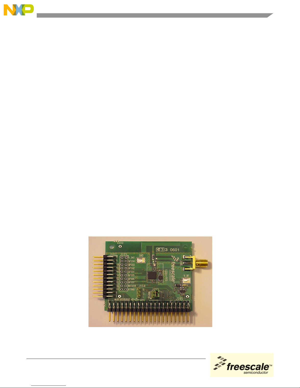
purposes. Figure 1-1 shows the RF Daughter Card.
Figure 1-1. MC1320x RF Daughter Card
© Freescale Semiconductor, Inc., 2006, 2007, 2008, 2009, 2010. All rights reserved.
Page 2
Introduction
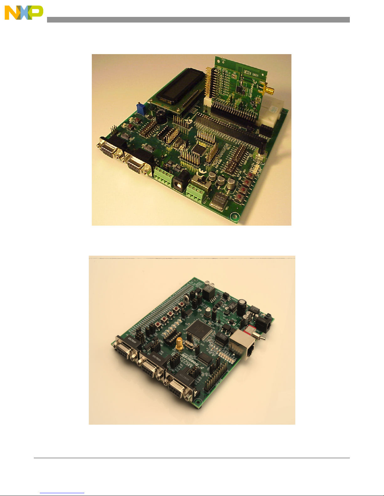
Figure 1-2 shows the RF Daughter Card installed in a GB60 development board.
Figure 1-2. MC1320xRF Daughter Card In GB60 Development Board
Figure 1-3 shows the M52235 EVB development board.
Figure 1-3. M52235 EVB Development Board
2 Freescale Semiconductor
MC1320x RF Daughter Card, Rev. 1.2
Page 3

Safety Information
2 Safety Information
Any modifications to this product may violate the rules of the Federal Communications Commission and
make operation of the product unlawful.
47 C.F.R. Sec. 15.21
This equipment has been tested and found to comply with the limits for a Class B digital device, pursuant
to part 15 of the FCC Rules. These limits are designed to provide reasonable protection against harmful
interference in a residential installation. This equipment generates uses and can radiate radio frequency
energy and, if not installed and used in accordance with the instructions, may cause harmful interference
to radio communications. However, there is no guarantee that interference will not occur in a particular
installation. If this equipment does cause harmful interference to radio or television reception, which can
be determined by turning the equipment off and on, the user is encouraged to try to correct the interference
by one or more of the following measures:
• Reorient or relocate the receiving antenna.
• Increase the separation between the equipment and receiver.
• Connect the equipment into an outlet on a circuit different from that to which the receiver is
connected.
• Consult the dealer or an experienced radio/TV technician for help.
47 C.F.R. Sec.15.105(b)
This equipment complies with FCC radiation exposure limits set forth for an uncontrolled environment.
The antenna(s) used for this equipment must be installed to provide a separation distance of at least 8
inches (20cm) from all persons.
This device complies with Part 15 of the FCC Rules. Operation is subject to the following two conditions:
• This device may not cause harmful interference.
• This device must accept any interference received, including interference that may cause undesired
operation.
3 Revision History
The following table summarizes revisions to this document since the previous release (Rev 1.1).
Revision History
Location Revision
Section 6 Updated document cross reference.
Freescale Semiconductor 3
MC1320x RF Daughter Card, Rev. 1.2
Page 4
MC1320x MCU Interface
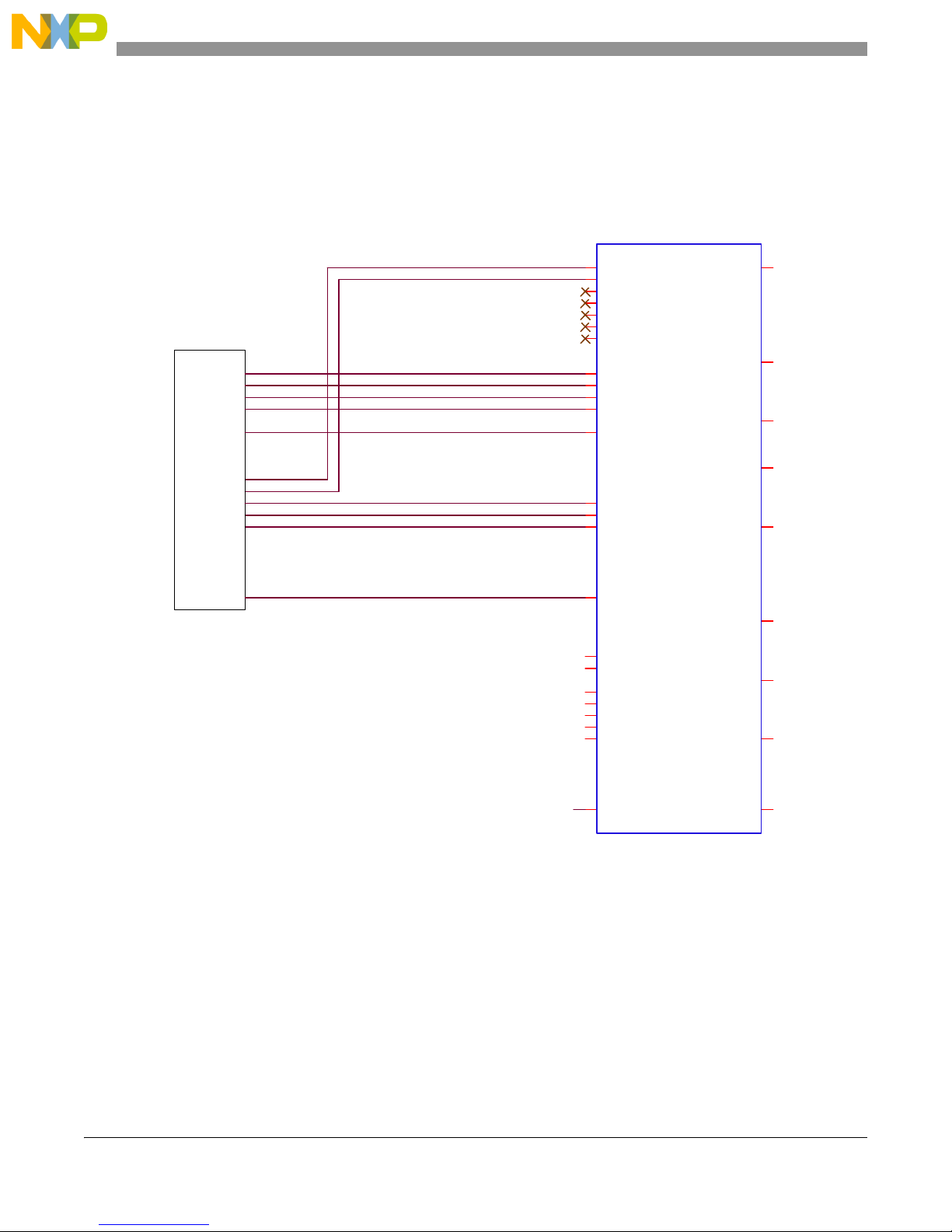
4 MC1320x MCU Interface
Figure 4-1 shows the typical connections between the MC1320x transceiver and a microcontroller unit
(MCU). See the MC13202/203 Reference Manual, document MC13202RM, for interface considerations.
Details about the interconnects for both the GB60 and M52235 Development boards are described in
Section 5.1, “Development Board Interconnects”.
MCU
SS
MISO
MOSI
SCLK
IR Q
GPIO
GPIO
GPIO
GPIO
GPIO
CLK
11
10
9
8
23
24
25
19
18
17
16
20
14
13
12
15
31
22
32
29
28
21
30
GPIO1
GPIO2
GPIO3
GPIO4
GPIO5
GPIO6
GPIO7
CEB
MISO
MOSI
SPICLK
IR Q B
ATTNB
RXTXEN
RSTB
CLKO
VBATT
VDDINT
VDDA
VDDLO1
VDDLO2
VDDD
VDDVCO
RIN_M
RIN_P
Not Used
Not Used
PAO_P
PAO_M
SM
XTAL1
1
2
3
4
5
6
7
26
4 Freescale Semiconductor
EP
Figure 4-1. MCU Interface Pinout
MC1320x RF Daughter Card, Rev. 1.2
GND
MC13202/3
XTAL2
27
Page 5
Daughter Card Description
5 Daughter Card Description
As shown in Figure 5-1 and Figure 8-1, connector J101 is the main interface to the GB60 Development
Board. The interface connections described in Section 5.1, “Development Board Interconnects”, fall under
the following three broad categories:
1. Serial Peripheral Interface (SPI)
2. Control
3. Power
Figure 1-2 shows how the RF Daughter Card is mounted on the GB60 Development Board.
NOTE
Ensure that zero ohm resistor R104 is in place on the MC1320x Daughter
Card. As of this release, previous versions of the MC1320x Daughter Card
may not have R104 inserted.
NOTE
J101 Pin 1 of the MC1320x must to be connected to GB_POR T Pin 1 of the
GB60 Development Board.
As shown in Figure 5-1 and Figure 8-1, connector J102 is the main interface to the M52235 Development
Board. Figure 1-3 shows how the RF Daughter Card is mounted on the M52235 Development Board.
NOTE
J102 Pin 1 of the MC1320x must be connected to MCU_POR T Pin 1 on the
M52235 Development Board.
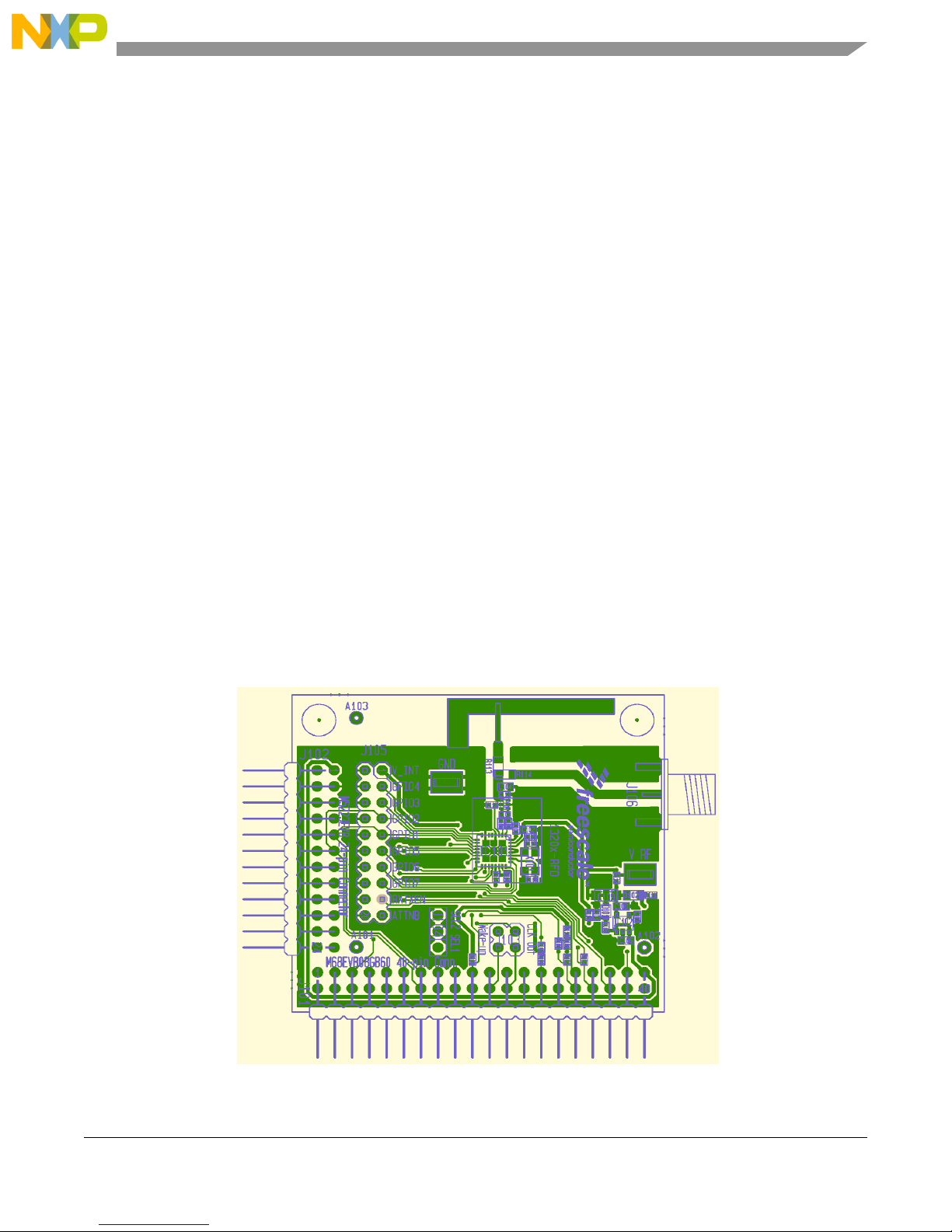
Figure 5-1 shows the top side of the RF Daughter Card PCB with component placement.
Figure 5-1. MC1320x Daughter Card (Top View)
Freescale Semiconductor 5
MC1320x RF Daughter Card, Rev. 1.2
Page 6

Daughter Card Description
Figure 5-2 shows the shows the bottom side of the RF Daughter Card PCB.
Figure 5-2. MC1320x Daughter Card (Bottom View)
5.1 Development Board Interconnects
The following sections describe the interconnects for both the GB60 and M52235 Development boards.
Table 5-1 lists the pin connections for J101 and Table 5-2 lists the pin connections for J102.
Table 5-1. J101 Pin Connections
Pin Number Pin Name Description Functionality
1,2,3,4, 6,7,8,9, 10,11,12,
15,16,17 18,21,23,
25,26,28, 29, 30,33
5 PT A2 Connects to PTA2 on GB60. Provides a wakeup function to the MCU via Pin
13 GPIO1 Connects to General Purpose
14 GPOI2 Connects to General Purpose
N/C No connection.
22 when jumper is installed between J103 pins
1 and 2.
When gpio_alt_en, Register 9, Bit 7 = 1,
Input/Output 1 of MC1320X.
Input/Output 2 of MC1320X.
GPIO1 functions as an “Out of Idle” Indicator.
When gpio_alt_en, Register 9, Bit 7 = 1,
GPIO2 functions as a “CRC Valid” Indicator.
6 Freescale Semiconductor
MC1320x RF Daughter Card, Rev. 1.2
Page 7

Daughter Card Description
Table 5-1. J101 Pin Connections (continued)
Pin Number Pin Name Description Functionality
19 IRQ Connects to IRQ pin of MC1320X. Allows the MC1320X to issue an IRQ to the
MCU.
20 RESET
Optionally connects to RESET of
Allows the MCU to reset the MC1320X.
MC1320X when R101 or R102 are
installed.
22 PTE1/RXD1 Connects to PTE1/RXD1 of GB60. Provides a wakeup function to the MCU via Pin
5 when jumper is installed between J103 pins
1 and 2.
24 XCLK/16MHz Connects to CLKO of MC1320X
when jumper is installed between
Provides reference based on MC1320X 16
MHz reference oscillator to the MCU.
J103 pins 3 and 4.
27 PTC2/BAUD
SEL
31 RXTXEN
Connect to PTC2/BAUD SEL of
GB60.
Connect to RXTXEN of MC1320X. Allows the MCU to control the RXTXEN line of
the MC1320X.
32 RESET
34 PTD5/CESI/A
TTN
Connects to RESET of MC1320X. Allows th e MCU to reset the MC1320X.
Connects to PTD5/CESI of GB60
when R104 is installed. Connect
Allows the MCU to wake up the MC1320X from
Doze or Hibernate.
directly to Pin 15 of J102.
35 MOSI Connect to MOSI of MC1320x. SPI
36 SPSCK Connect to SPICLK of the
SPI
MC13201.
37 CE Connect to CE of MC1320X. SPI
38 MISO Connects to MISO of MC1320X. SPI
39 V_IN Connects the Daughter Card to the
supply voltage output of the GB60
board.
Provides supply voltage to the Daughter Card.
Voltage must not exceed 16 Vdc. See
Section 5.1.0.3, “Power Connections”.
40 GND Connect ground on GB60 board to
ground on Daughter Card.
MC1320x RF Daughter Card, Rev. 1.2
Freescale Semiconductor 7
Page 8

Daughter Card Description
Table 5-2. J102 Pin Connections
Pin Number Pin Names Description Functionality
4, 5, 6, 7, 8, 11, 12, 14,
16, 18, 22
1 V_IN Connects the Daughter Card to the
2IRQ
3 GND Connects the ground of the RF
9 GPIO1 Connects to General Purpose
10 GPOI2 Connects to General Purpose
13 RESET
15 PTD5/CESI Connects to ATTN
N/C No connection
Provides supply voltage to the Daughter Card.
supply voltage output on the
M52235EVB.
Voltage must not exceed 16 Vdc. See
Section 5.1.0.3, “Power Connections”.
Connects to IRQ pin of MC1320X. Allows the MC1320X to issue an IRQ to the
MCU.
Daughter Card to the ground of the
M52235EVB
When gpio_alt_en, Register 9, Bit 7 = 1,
Input/Output 1 of MC1320X.
GPIO1 functions as an “Out of Idle” Indicator.
When gpio_alt_en, Register 9, Bit 7 =1,
Input/Output 2 of MC1320X.
Connects to RESET of MC1320X
GPIO2 functions as a “CRC Valid” Indicator.
Allows the MCU to reset the MC1320X.
and Pin 32 of J101.
of MC1320X
and Pin 34 of J101.
Allows the MCU to wake up the MC1320X
from Doze or Hibernate.
17 MOSI Connects to MOSI of MC1320X. SPI
19 MISO Connects to MISO of MC1320X. SPI
20 RXTXEN
Connect to RXTXEN of MC1320X. Allows the MCUntrol the RXTXEN line of the
MC1320X.
21 SPICLK Connect to SPICLK of the
SPI
MC1320X
23 PTE2/CE-
QSPI-CSO
Connects to Pin 1 of J104 Allows Chip Enable (CE) selection.
See Section 5.1.0.1, “SPI Connections”.
24 PTE2/CE-AN7 Connects to Pin 3 of J104 Allows Chip Enable (CE) selection.
See Section 5.1.0.1, “SPI Connections”.
MC1320x RF Daughter Card, Rev. 1.2
8 Freescale Semiconductor
Page 9

Daughter Card Description
NOTE
In the following sections, pin numbers not in parenthesis reference the
GB60 Development Board. Pin numbers in parenthesis reference the
M52235 Development Board.
5.1.0.1 SPI Connections
J101 pins 35 through 38 (J102 pin 17, 19, 21 and 23) provide the following four wire SPI interface:
•MOSI
• SPICLK
•CE
•MISO
The MC1320x always functions as a slave device. SPI operation is described in detail in the appropriate
MC1320x Data Sheet and/or MC1320x Reference Manual.
NOTE
As it applies to the M52235 Development Board, the CE signal on (J102 Pin
23 and Pin 24) are hard wired to header J104. These pins control the
functionality of CE.
When Pin 2 and Pin 3 of J104 are shorted, CE is wired to (J102 Pin 24)
(PTE2/CE-AN7).
When Pin 1 and Pin 2 of J104 are shorted, CE is wired to (J102 Pin 23)
(P TE2/CE-QSPI_CS0).
5.1.0.2 Control Connections
• J101 Pin 19 (J102 Pin 2) is the IRQ line from the MC1320x. Connection to the MCU depends on
how the MCU services interrupts.
• J101 Pin 31 (J102 Pin 20), RXTXEN, allows the MCU to initiate transceiver functions.
• J101 Pin 34 (J102 Pin 15), ATTN
Hibernate low power modes.
RXTXEN and ATTN are also available at header J105 for manual control.
• J101 Pin 24 provides the MC1320x CLKO to the MCU when a jumper is installed at J103.
• J101 Pin 32 (J102 Pin13) interfaces with the MCU to provide a Reset to the MC1320x.
• J101 Pin 5 and Pin 22 provide a wake up function to the MCU when a jumper is installed at J103.
• J101 Pin 13 and Pin 14 (J102 Pin 9 and Pin 11) provide access to the MC1320x GPIO1 and GPIO2
ports.
, allows the MCU to wake up the MC1320x from Doze or
NOTE
Freescale Semiconductor 9
MC1320x RF Daughter Card, Rev. 1.2
Page 10

RF Circuit
5.1.0.3 Power Connections
J101 Pin 39 (J102 pin 1) provides the supply voltage to the RF Daughter Card. Voltage on this line should
never exceed 16.0 VDC and the nominal voltage supply should not exceed 16.0 VDC. J101 Pin 40 (J102
pin 3) is ground.
NOTE
MCU connection signals are dependent on the on-board voltage regulator.
If R105, D101, and C101 are mounted and R115 is removed, J101 Pin 39
will provide the interface supply voltage which must never exceed 3.6 V.
Nominal supply voltage should never exceed 3.4 V.
5.1.0.4 Non-MCU Connections
Header J105 provides connections to a number of MC1320x contacts for non-MCU connections. As
already stated, the RXTXEN and ATTN lines are available at J105 for external control using switches or
other hardware. The MC1320x GPIO is also available for connection to external hardware.
6RF Circuit
The MC1320x has an internal TX/RX switch. This feature allows for an external RF circuit that has a very
low component count. The MC1320x requires only a few passive components and a balun to provide an
interface to an antenna or a 50 ohm circuit. Figure 6-1 shows a schematic for only the RF portion of the
MC1320x Daughter Card.
Figure 6-1. RF Portion of 20x Daughter Card
10 Freescale Semiconductor
MC1320x RF Daughter Card, Rev. 1.2
Page 11

Software Configuration
To provide a design that is of the lowest possible cost to produce, this reference design was built on a
printed circuit board consisting of only two layers and with a printed circuit board antenna. The antenna
is an Inverted F design widely used in the 2.4 GHz band. This antenna provides good performance while
minimizing Bill of Material (BOM) cost.
For more information on a low cost design approach, see the ZigBee Hardware Design Considerations
Reference Manual (ZHDCRM)
7 Software Configuration
As shown in Figure 8-1, the legend in the schematic shows the recommended jumper settings for Wake,
ClkOut, and Chip Enable.
NOTE
The Wake and ClkOut signals are only for interface to the GB60
Development Board. The Chip Enable signal is only for interface to the
M52235 Development Board.
For software development, Freescale recommends users obtain the most recent software development
tools and documentation from the following web pages:
• For ZigBee related software and documentation go to www.freescale.com/zigbee
• For microcontroller software and documentation go to www.codewarrior.com
Freescale Semiconductor 11
MC1320x RF Daughter Card, Rev. 1.2
Page 12

Bill of Materials (BOM) and Schematic
8 Bill of Materials (BOM) and Schematic
This section contains the RF Daughter Card BOM and schematic.
Table 8-1. Bill of Materials
Qty Part Number Value
1 96000310100 Label 21*6mm
Test BarCode
3 50610710001 100nF 16V
±10% X7R
0 50610710001 100nF 16V
±10% X7R
2 50620810001 1µF 6.3V
±10% X5R
0 50620810001 1µF 6.3V
±10% X5R
0 50610610000 10nF 16V
±10% X7R
1 53300833001 3.3µF 10V
20%
2 50210268000 6.8pF 50V
±0.25pF NP0/C0G
1 50210310000 10pF 50V
±5% NP0/C0G
Rating
Tolerance
Manufacturer Part Number Reference
96000310100 BARCODE101
Murata GRM155R71C10 4KA88D C103, C104,
C105
Murata GRM155R71C10 4KA88D C101 (Not
Mounted)
Murata GRM188R60J105KA01D C102, C106
Murata GRM188R60J105KA01D C108 (Not
Mounted)
Murata GRM155R71E103KZ01E C107(Not
Mounted)
Vishay Sprague 293D335X0010A2TE3 C109
Murata GRM1555C1H6R8DZ01J C110, C111
Murata GRM1555C1H100JZ01D C112
1 50210210000 1.0pF 50V
±0.25pF NP0/C0G
0 40110003303 MM3Z3V3T1G 3.3V/200mW
5%
1 41100017001 Green_LED Citizen CL-170G-CD-T D102
1 35501320200 MC13202 Freescale
1 34000298109 LP2981IM5-3.3 -40 to +125°C National LP2981IM5-3.3 NOPB IC102
1 20030404001 2*20p Pin
Header - Right
Angle
1 20030402401 2*12p Pin
Header - Right
Angle
1 20030400400 2*2p Pin
Header
1 20030400300 jumper_1x3 AMP 826629-3 J104
mot/molex70216-40 10-89-4402 J101
mot/molex70216-24 10-89-4242 J102
Murata GRM1555C1H1R0CZ01D C113
ON
Semiconductor
Semiconductor
AMP 0-826632-2 J103
MM3Z3V3T1G D101 (Not
Mounted)
MC13202 IC101
12 Freescale Semiconductor
MC1320x RF Daughter Card, Rev. 1.2
Page 13

Table 8-1. Bill of Materials
Bill of Materials (BOM) and Schematic
Qty Part Number Value
0 20030402008 2*10 Pin
Header
1 20150700202 SMA_edge_Re
mot/sma-end_launch 142-0701-831 J106
Rating
Tolerance
Manufacturer Part Number Reference
AMP 1-826632-0 J105 (Not
Mounted)
ceptacle_Fema
le
2 20030000100 ProbeLoop Toby
TP-107-02-5-T J107, J108
Electronics
2 54710518001 1.8nH 300mA
TOKO LL1005-FHL1N8S L101, L102
±0.3nH
2 54710539002 3.9nH ±0.3nH TOKO LL1005-FHL3N9S L103, L104
1 71000566010 fsl566-1 Freescale
FSL566-1 FR4 0.76mm PCB101
Semiconductor
4 61100000001 0R 62.5mW/25V
5%
0 61100000001 0R 62.5mW/25V
5%
YAGEO RC0402JRE070RL R103, R112,
R115,R104
YAGEO RC0402JRE070RL R101, R102
(Not
Mounted)
0 61100410001 100R 62.5mW/25V
5%
YAGEO RC0402JRE07100RL R105 (Not
Mounted)
0 61100610001 10K 62.5mW/25V
5%
1 61100747000 470K 62.5mW/25V
5%
1 61100422000 220R 62.5mW/25V
5%
1 61120000001 0R 125mW/150V
5%
0 61120000001 0R 125mW/150V
5%
1 58130916004 16.000MHz ±20ppm
±20ppm
1 56360240001 LDB212G4005
C-001
YAGEO RC0402JRE0710KL R106, R107,
R108, R110
(Not
Mounted)
YAGEO RC0402JRE07470KL R109
YAGEO RC0402JRE07220RL R111
YAGEO RC0805JRE070RL R113
YAGEO RC0805JRE070RL R114 (Not
Mounted)
KDS ZD00882 X101
Murata LDB212G4005C-001 Z101
Freescale Semiconductor 13
MC1320x RF Daughter Card, Rev. 1.2
Page 14

14 MC1320x RF Daughter Card Rev. 1.2 Freescale Semiconductor
Figure 8-1. Daughter Card Schematic
5
4
3
2
1
D D
C C
B B
A A
GPIO3
PTE4/MOSI
RXTXEN
GPIO2
PTE5/SPSCK
GPIO1
VCC
GPIO6
PTE3/MISO
PTD5/CESi
GPIO2
ATTNB
GPIO5
GPIO1
CLKO
GPIO7
GPIO4
PTE2/CE
GPIO2
PTD6/RXTXEN
CLKO
PTE2/CE-QSPI-CS0
GND
PTE2/CE-AN7
PTE5/SPSCK
PTE4/MOSI
PTD5/CESi
PTE2/CE
PTE4/MOSI
PTA2
PTC2/BAUD_SEL
PTE3/MISO
PTE3/MISO
IRQ
GPIO1
V_IN
XCLK/16MHz
GPIO2
PTE1/RXD1
GPIO1
PTD6/RXTXEN
PTD6/RXTXEN
IRQ
PTE2/CE
PTC2/BAUD_SEL
PTE5/SPSCK
PTD7/RESET
PTD7/RESET
IRQ
V_RFV_IN
V_RF
V_INT
V_RF
V_INT
V_INT
V_IN
V_IN
V_INT
V_RF
Title
Size Document Number
Rev
Date: Sheet
of
© Freescale Semiconductor
80000566000_R0103.DSN R01.03
1320x-RFD - for ColdFire/HCS08 (FSL566-1): Main Schematic
2100 East Elliot Drive
Tempe, AZ, USA
A3
11Wednesday, May 23, 2007 JJ/ALA/HBR
2007
www.freescale.com
Title
Size Document Number
Rev
Date: Sheet
of
© Freescale Semiconductor
80000566000_R0103.DSN R01.03
1320x-RFD - for ColdFire/HCS08 (FSL566-1): Main Schematic
2100 East Elliot Drive
Tempe, AZ, USA
A3
11Wednesday, May 23, 2007 JJ/ALA/HBR
2007
www.freescale.com
Title
Size Document Number
Rev
Date: Sheet
of
© Freescale Semiconductor
80000566000_R0103.DSN R01.03
1320x-RFD - for ColdFire/HCS08 (FSL566-1): Main Schematic
2100 East Elliot Drive
Tempe, AZ, USA
A3
11Wednesday, May 23, 2007 JJ/ALA/HBR
2007
www.freescale.com
PWR
GPIO
M68EVB08GB60 - GP_Port
M5223EVB - MCU Port
2-3
J104
1-2 QSPI-CS0 (default)
AN7
Chip Enable Select
3-4
J103
1-2
Wake up enabled, no Clock out.
No Wake up, no Clock out.
16MHz Clock Out & Wake Up Select
1-2 & 3-4
All off
No Wake up, Clock out enabled. (default)
Wake up enabled, Clock out enabled.
Chip Enable
Select
16MHz Clock Out & Wake-up
Select
NOTE 1: R104 should be placed to enable all low power modes.
L103
3.9nH
L103
3.9nH
A102
'Secundary_fiducial_point_(Compside)'
A102
'Secundary_fiducial_point_(Compside)'
C113
1.0pF
C113
1.0pF
C111
6.8pF
C111
6.8pF
R109
470K
R109
470K
J103
2*2p Pin Header
J103
2*2p Pin Header
1 2
3 4
R107
10K
Not Mounted
R107
10K
Not Mounted
R105
100R
Not Mounted
R105
100R
Not Mounted
.HOLE102
'np_hole_ø2.0mm'
.HOLE102
'np_hole_ø2.0mm'
C101
100nF
Not Mounted
C101
100nF
Not Mounted
A103
'Secundary_fiducial_point_(Soldside)'
A103
'Secundary_fiducial_point_(Soldside)'
D102
Green_LED
D102
Green_LED
R1120RR112
0R
R102
0R
Not Mounted
R102
0R
Not Mounted
C110
6.8pF
C110
6.8pF
BARCODE101
Label 21*6mm Test BarCode
BARCODE101
Label 21*6mm Test BarCode
Z101
LDB212G4005C-001
Z101
LDB212G4005C-001
5
1
6
2
3
4
R108
10K
Not Mounted
R108
10K
Not Mounted
A101
'Primus_datum_point_(Compside)'
A101
'Primus_datum_point_(Compside)'
J102
2*12p Pin Header - Right Angle
J102
2*12p Pin Header - Right Angle
12
34
6
8
10
12
14
18
20
5
7
9
11
13
15
17
19
16
2122
2324
R1150RR115
0R
TP103TP103
D101
MM3Z3V3T1G
Not Mounted
D101
MM3Z3V3T1G
Not Mounted
2 1
C109
3.3μF
C109
3.3μF
J104
jumper_1x3
J104
jumper_1x3
1
2
3
IC102
LP2981IM5-3.3
IC102
LP2981IM5-3.3
IN1OUT
5
ON/OFF3GND
2
NC
4
C103
100nF
C103
100nF
R1130RR113
0R
J101
2*20p Pin Header - Right Angle
J101
2*20p Pin Header - Right Angle
12
34
6
8
10
12
14
18
20
5
7
9
11
13
15
17
19
16
2122
2324
2526
2728
2930
3132
3334
3536
3738
3940
C112
10pF
C112
10pF
C104
100nF
C104
100nF
L104
3.9nH
L104
3.9nH
J106
SMA_edge_Receptacle_Female
J106
SMA_edge_Receptacle_Female
1
2
5
3
4
R101
0R
Not Mounted
R101
0R
Not Mounted
IC101
MC13202
IC101
MC13202
ATTNBi
14
CEBi
19
CLKOo
15
GPIO1
11
GPIO2
10
GPIO3
9
GPIO4
8
GPIO7
25
GPIO5
23
GPIO6
24
IRQBo
20
MISOo
18
MOSIi
17
PAO_M
6
PAO_P
5
RIN_M
1
RIN_P
2
RSTBi
12
RXTXENi
13
GND
7
SPICLKi
16
GND
4
CT_Bias
3
XTAL1
26
XTAL2
27
VBATT
31
VDDA
32
VDDD
21
VDDINT
22
VDDLO1
29
VDDLO2
28
VDDVCO
30
GND
33
ANT100
F_Antenna
ANT100
F_Antenna
C106
1μF
C106
1μF
TP102TP102
J107
ProbeLoop
J107
ProbeLoop
J105
2*10 Pin Header
Not Mounted
J105
2*10 Pin Header
Not Mounted
12
34
6
8
10
12
14
18
20
5
7
9
11
13
15
17
19
16
L102
1.8nH
L102
1.8nH
R114
0R
Not Mounted
R114
0R
Not Mounted
PCB101
fsl566-1
PCB101
fsl566-1
X101
16.000MHz
X101
16.000MHz
TP101TP101
C107
10nF
Not Mounted
C107
10nF
Not Mounted
R106
10K
Not Mounted
R106
10K
Not Mounted
R110
10K
Not Mounted
R110
10K
Not Mounted
L101
1.8nH
L101
1.8nH
R111
220R
R111
220R
R104
0R
NOTE 1
R104
0R
NOTE 1
C102
1μF
C102
1μF
C108
1μF
Not Mounted
C108
1μF
Not Mounted
.HOLE101
'np_hole_ø3.0m'
.HOLE101
'np_hole_ø3.0m'
C105
100nF
C105
100nF
J108
ProbeLoop
J108
ProbeLoop
R1030RR103
0R
Page 15

NOTES
MOTOROLA MC1320x RF Daughter Card, Rev. 1.2 15
Page 16

How to Reach Us:
Home Page:
www.freescale.com
E-mail:
support@freescale.com
USA/Europe or Locations Not Listed:
Freescale Semiconductor
Technical Information Center, CH370
1300 N. Alma School Road
Chandler, Arizona 85224
+1-800-521-6274 or +1-480-768-2130
support@freescale.com
Europe, Middle East, and Africa:
Freescale Halbleiter Deutschland GmbH
Technical Information Center
Schatzbogen 7
81829 Muenchen, Germany
+44 1296 380 456 (English)
+46 8 52200080 (English)
+49 89 92103 559 (German)
+33 1 69 35 48 48 (French)
support@freescale.com
Japan:
Freescale Semiconductor Japan Ltd.
Headquarters
ARCO Tower 15F
1-8-1, Shimo-Meguro, Meguro-ku,
Tokyo 153-0064, Japan
0120 191014 or +81 3 5437 9125
support.japan@freescale.com
Asia/Pacific:
Freescale Semiconductor Hong Kong Ltd.
Technical Information Center
2 Dai King Street
Tai Po Industrial Estate
Tai Po, N.T., Hong Kong
+800 2666 8080
support.asia@freescale.com
For Literature Requests Only:
Freescale Semiconductor Literature Distribution Center
P.O. Box 5405
Denver, Colorado 80217
1-800-521-6274 or 303-675-2140
Fax: 303-675-2150
LDCForFreescaleSemiconductor@hibbertgroup.com
Information in this document is provided solely to enable system and software implementers to use
Freescale Semiconductor products. There are no express or implied copyright licenses granted
hereunder to design or fabricate any integrated circuits or int egrated circuits based on the informa tion
in this document.
Freescale Semiconductor reserves the right to make changes without furt her notice to any product s
herein. Freescale Semiconductor makes no warranty, representation or guarantee regarding the
suitability of its products for any particular purpose, nor does Freescale Semiconductor assume any
liability arising out of the application or use of any product or circuit, and specifically disclaims any
and all liability, including without limitation consequential or incident al damages. “Typical” parameters
that may be provided in Freescale Semiconductor data sheet s and/or specifications can and do vary
in different applications and actual performance may vary over time. All operating parameters,
including “Typicals”, must be vali dated for each customer application by customer’s technical
experts. Freescale Semiconductor does not convey any l icense und er it s paten t rights no r the right s
of others. Freescale Semiconductor products are not designed, intended, or authorized for use as
components in systems intended for surgical implant into the body, or other applications intended to
support or sustain life, or for any other applicatio n in which the failure of the Freescale Semiconductor
product could create a situation where personal injury or death may occur. Should Buyer purchase
or use Freescale Semiconductor products for any such unintended or unauthorized application,
Buyer shall indemnify and hold Freescale Semiconductor and its officers, employees, subsidiaries,
affiliates, and distributors harmless against all claims, costs, damages, and expenses, and
reasonable attorney fees arising out of, directly or indirectly, any claim of personal injury or death
associated with such unintended or unauthorized use, even if such claim alleges that Freescale
Semiconductor was negligent regarding the design or manufacture of the part.
Freescale™ and the Freescale logo are trademarks of Freescale Semiconductor, Inc. All other
product or service names are the property of their respective owners.
© Freescale Semiconductor, Inc. 2006, 2007, 2008, 2009, 2010. All rights reserved.
Docu m e n t N um b e r : MC1320xRFCUG
Rev. 1.2
03/2010
 Loading...