

Page 1

Motorola, Inc.
Application Development System
Freescale Semiconductor, Inc.
M68VZ328ADS
nc...
User’s Manual
Revision 1.4
Sep 4, 2000
Freescale Semiconductor, I
Motorola reserves the right to make changes without further notice to any product herein to improve
reliability, function, or design. Motorola does not assume any liability arising out of the application or
use of any product, circuit, or software described herein; neither does it convey any license under its
patent rights nor the rights of others. Motorola products are not designed, intended, or authorized for use
as components in systems intended for surgical implant into the body, or other applications intended to
support life, or for any other application in which the failure of the Motorola product could create a
situation where personal injury or death may occur. Should Buyer purchase or use Motorola products for any
such intended or unauthorized application, Buyer shall indemnify and hold Motorola and its officers,
employees, subsidiaries, affiliates, and distributors harmless against all claims, costs, damages, and
expenses, and reasonable attorney fees arising out of, directly or indirectly, any claim of personal injury
or death associated with such unintended or unauthorized use, even if such claim alleges that Motorola was
negligent regarding the design or manufacture of the part. Motorola and the are registered trademarks
of Motorola Ltd.
For More Information On This Product,
Go to: www.freescale.com
Page 2

nc...
Freescale Semiconductor, Inc.
TABLE OF CONTENTS
Section 1
General Information
1.1 Introduction...................................................................................................1-7
1.2 Features........................................................................................................1-7
1.3 Related Documentation ................................................................................1-8
1.4 Technical Support.........................................................................................1-8
1.4.1 M68VZ328ADS...........................................................................................1-8
1.4.2 Debugger....................................................................................................1-8
Section 2
Quick Installation Guide
2.1 Overview.......................................................................................................2-9
2.2 Equipments Required ...................................................................................2-9
2.3 Installation Procedure ...................................................................................2-9
2.3.1 Prepare the M68VZ328ADS board.............................................................2-9
2.3.2 Connecting M68VZ328ADS to PC............................................................2-12
2.3.3 Installing software debugger.....................................................................2-12
Section 3
Hardware Description and Board Operation
3.1 Overview.....................................................................................................3-17
3.2 Control Switches.........................................................................................3-18
3.3 DIP Switches...............................................................................................3-18
3.4 Operation Modes ........................................................................................3-18
3.5 LED Indicators ............................................................................................3-19
3.6 Memory.......................................................................................................3-19
3.6.1 Memory Map.............................................................................................3-19
Freescale Semiconductor, I
3.6.2 FLASH Memory ........................................................................................3-20
3.6.3 SDRAM.....................................................................................................3-21
3.7 UART and IRDA..........................................................................................3-22
3.8 LCD and Touch Panel Interface..................................................................3 -23
3.8.1 LCD Interface............................................................................................3-23
3.8.2 Touch Panel Interface...............................................................................3-24
3.9 Single Tone Generator................................................................................3-25
3.10 Logic Analyzer Interface .............................................................................3-25
3.11 ExPANSION Connectors ............................................................................3-26
3.12 Power Supply..............................................................................................3-27
Appendix A
MOTOROLA M68VZ328ADS USER’S MANUAL ii
For More Information On This Product,
Go to: www.freescale.com
Page 3

Freescale Semiconductor, Inc.
A.1 General Concepts of Resistive Panels .......................................................A-29
Programming On-board Flash Memory
B.1 Overview.....................................................................................................B-31
B.2 Elements for programming the flash...........................................................B-31
B.3 Method........................................................................................................B-32
B.4 Offset Address of ROM Image....................................................................B-32
B.5 Executing ProgRam Command Sequence .................................................B-33
Table of Contents
Resistive Touch Panel Operation
Appendix B
Appendix C
Monitor Initialization Code
nc...
C.1 Initialization Code of Metrowerks Monitor (Reset.S)..................................C-39
C.2 Initialization Code of SDS Monitor (Monitor.H)..........................................C-43
Appendix D
Schematics
D.1 M68VZ328ADS..........................................................................................D-57
Freescale Semiconductor, I
MOTOROLA M68VZ328ADS USER’S MANUAL iii
For More Information On This Product,
Go to: www.freescale.com
Page 4

nc...
Table of Contents
Freescale Semiconductor, Inc.
Freescale Semiconductor, I
iv M68VZ328ADS USER’S MANUAL MOTOROLA
For More Information On This Product,
Go to: www.freescale.com
Page 5

nc...
Freescale Semiconductor, Inc.
LIST OF ILLUSTRATIONS
2-1 M68VZ328ADS Key Component Layout..........................................................2-10
2-2 Default DIP Switch Options for Metrowerks monitor using UART1..................2-11
2-3 DIP Switch Options for Metrowerks monitor using UART2 ..............................2-11
2-4 DIP Switch Options for SDS monitor using UART1 .........................................2-11
2-5 DIP Switch Options for SDS monitor using UART2 .........................................2-11
2-6 Connecting PC to UART1 of M68VZ328ADS ..................................................2-12
2-7 Debug Pop-Up Window of SDS v7.4................................................................2 -15
2-8 Connection Setting inside Debug Pop-up Window of SDS v7.4 ......................2-16
3-1 M68VZ328ADS Functional Block Diagram ......................................................3-17
3-2 Interface of Flash Memories.............................................................................3-20
3-3 Interface of SDRAMs........................................................................................3-21
3-4 UART and IRDA Interface................................................................................3-22
3-5 Serial Port Pin Assignment...............................................................................3-22
3-6 LCD and Touch Panel Connector Pin Assignment ..........................................3-23
3-7 Touch Panel Controller Interface......................................................................3-24
3-8 Single Tone Generator.....................................................................................3-25
3-9 Logic Analyzer Connectors ..............................................................................3-25
3-10 Power Connectors............................................................................................3-27
1-1 Resistive Touch Panel......................................................................................A-29
1-2 Determination of X,Y Position ..........................................................................A-30
B-1 Method of programming on-board Flash memory............................................B-32
B-2 Flash Program Algorithm..................................................................................B-37
Freescale Semiconductor, I
MOTOROLA M68VZ328ADS USER’S MANUAL v
For More Information On This Product,
Go to: www.freescale.com
Page 6

nc...
Freescale Semiconductor, Inc.
LIST OF TABLES
3-1 DIP Switch pack S1 Setting..............................................................................3-18
3-2 DIP Switch pack S2 Setting..............................................................................3-18
3-3 Operation Mode Setting ...................................................................................3-19
3-4 Function of LED Indicators...............................................................................3-19
3-5 M68VZ328ADS Default Memory Map..............................................................3-19
3-6 Possible Configuration of FLASH Memories....................................................3-20
3-7 Signal Assignment for Touch Panel Controller.................................................3-24
3-8 Pin Assignments of P7.....................................................................................3-26
3-9 Pin Assignment of P9.......................................................................................3-27
Freescale Semiconductor, I
MOTOROLA M68VZ328ADS USER’S MANUAL vi
For More Information On This Product,
Go to: www.freescale.com
Page 7

Freescale Semiconductor, Inc.
SECTION 1
GENERAL INFORMATION
1.1 INTRODUCTION
The DragonBallTM-VZ (MC68VZ328) Application Development System (M68VZ328ADS) is
designed to supply users with an environment to develop MC68VZ328 based application
software. Moreover, this board can be used as a reference for real-life product design.
M68VZ328ADS provides several interface ports for application software and target board
debug purpose. This document will discuss the usage and system details of the
M68VZ328ADS.
1.2 FEATURES
• MC68VZ328 CPU
nc...
• Memory Subsystem
—4 MB FLASH
—8 MB SDRAM (Expandable to 16 MB)
• Debug ports
—Two RS232 serial ports interface to MC68VZ328 internal UARTs
—Direct logic analyzer interface to system bus
• LCD and Touch Panel Interface
—MC68VZ328 LCD interface
—Burr-Brown 12-bit touch panel controller ADS7843E available for pen input
•LEDIndicators
—Red LED for power
—Green LED for system heart beat
—Yellow LED for status of MC68VZ328 pin PD0
—Yellow LED for status of MC68VZ328 pin PD1
• Board operation mode support
—MC68VZ328 normal mode
—MC68VZ328 bootstrap mode
Freescale Semiconductor, I
• Debug Monitor
—MetroWerks Codewarrior Target Monitor using serial port
—SDS source-leveldebugger monitor by Software Development SystemInc. using se-
rial port
• Clock Source
—32.768KHz for MC68VZ328 internal PLL
• Power Supply
—3.0V - 3.3V main power supply
MOTOROLA M68VZ328ADS USER’S MANUAL 1-7
For More Information On This Product,
Go to: www.freescale.com
Page 8

nc...
General Information
Freescale Semiconductor, Inc.
1.3 RELATED DOCUMENTATION
The following documents can be used as references when using M68VZ328ADS.
• MC68VZ328 User’s Manual
• MC68VZ328 Product Information
1.4 TECHNICAL SUPPORT
1.4.1 M68VZ328ADS
For getting the latest information, please visit our web page:
http://www.mot.com/SPS/WIRELESS/products/DragonBall.html
http://www.apspg.com/products.html
1.4.2 Debugger
There are three source-level debuggers for DragonBallTM-VZ. The contact information is
listed below.
1. Metrowerks
http://www.metrowerks.com
2. Single Step Development
http://www.sdsi.com
3. Microtek SLD
http://www.microtekintl.com
Freescale Semiconductor, I
1-8 M68VZ328ADS USER’S MANUAL MOTOROLA
For More Information On This Product,
Go to: www.freescale.com
Page 9

nc...
Freescale Semiconductor, Inc.
SECTION 2
QUICK INSTALLATION GUIDE
2.1 OVERVIEW
This section provides a description of the evaluation module, requirements, quick installation and test information. Detailed information on the M68VZ328ADS design and operation
is provided in the remaining sections of this manual.
2.2 EQUIPMENTS REQUIRED
The following equipments are required to use with the M68VZ328ADS Application Development System, some of them are already bundled with the ADS package.
• Powersupply − 3.0V-3.3V,1500mA, with 2 mm female (inside positive)power connector
• RS-232cable(DB9maletoDB9female)
• IBMPC compatible computer (486 class or higher) runningWindows3.1 and DOS 6.0
(or higher), or Windows 95, with an RS-232 serial port capable of 9600-115200 bit per
second operation
2.3 INSTALLATION PROCEDURE
Pls. follow the procedure below to set up M68VZ328ADS.
1. Prepare the M68VZ328ADS board
2. Connect the M68VZ328ADS board to PC and power supply
3. Install software debugger
2.3.1 Prepare the M68VZ328ADS board
Locate the DIP switches on the M68VZ328ADS board and select appropriate monitor and
debug port for your debugger.
Figure2-2 shows thefactory defaultDIP switches settings.This settingselects to useMetro-
Freescale Semiconductor, I
works monitor and UART1 of DragonBall-VZ as the debug port. Other possible settings are
showninFigure2-3,Figure2-4andFigure2-5.
For detail description of each switch. Pls. refer to Table 3-1 and Table 3-2.
For additional information on the M68VZ328ADS and its components. Pls refer to Section 3 .
MOTOROLA M68VZ328ADS USER’S MANUAL 2-9
For More Information On This Product,
Go to: www.freescale.com
Page 10
nc...
Quick Installation Guide
Freescale Semiconductor, Inc.
Freescale Semiconductor, I
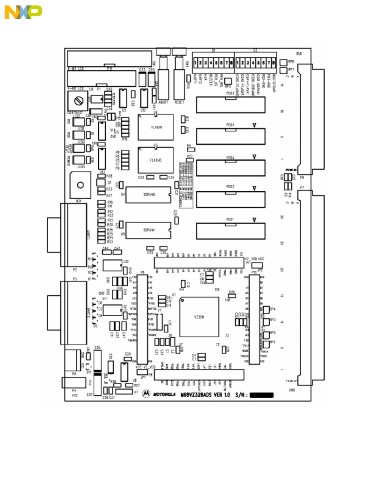
Figure 2-1. M68VZ328ADS Key Component Layout
2-10 M68VZ328ADS USER’S MANUAL MOTOROLA
For More Information On This Product,
Go to: www.freescale.com
Page 11

Quick Installation Guide
Monitor and Debug port selection
Freescale Semiconductor, Inc.
nc...
S1
ON
12345678
Figure 2-2. Default DIP Switch Options for Metrowerks monitor using UART1
S1
ON
12345678
Figure 2-3. DIP Switch Options for Metrowerks monitor using UART2
S2
ON
12345678
S2
ON
12345678
S1
ON
12345678
Freescale Semiconductor, I
Figure 2-4. DIP Switch Options for SDS monitor using UART1
S1
ON
12345678
Figure 2-5. DIP Switch Options for SDS monitor using UART2
S2
ON
12345678
S2
ON
12345678
2-11 M68VZ328ADS USER’S MANUAL MOTOROLA
For More Information On This Product,
Go to: www.freescale.com
Page 12
nc...
Quick Installation Guide
Freescale Semiconductor, Inc.
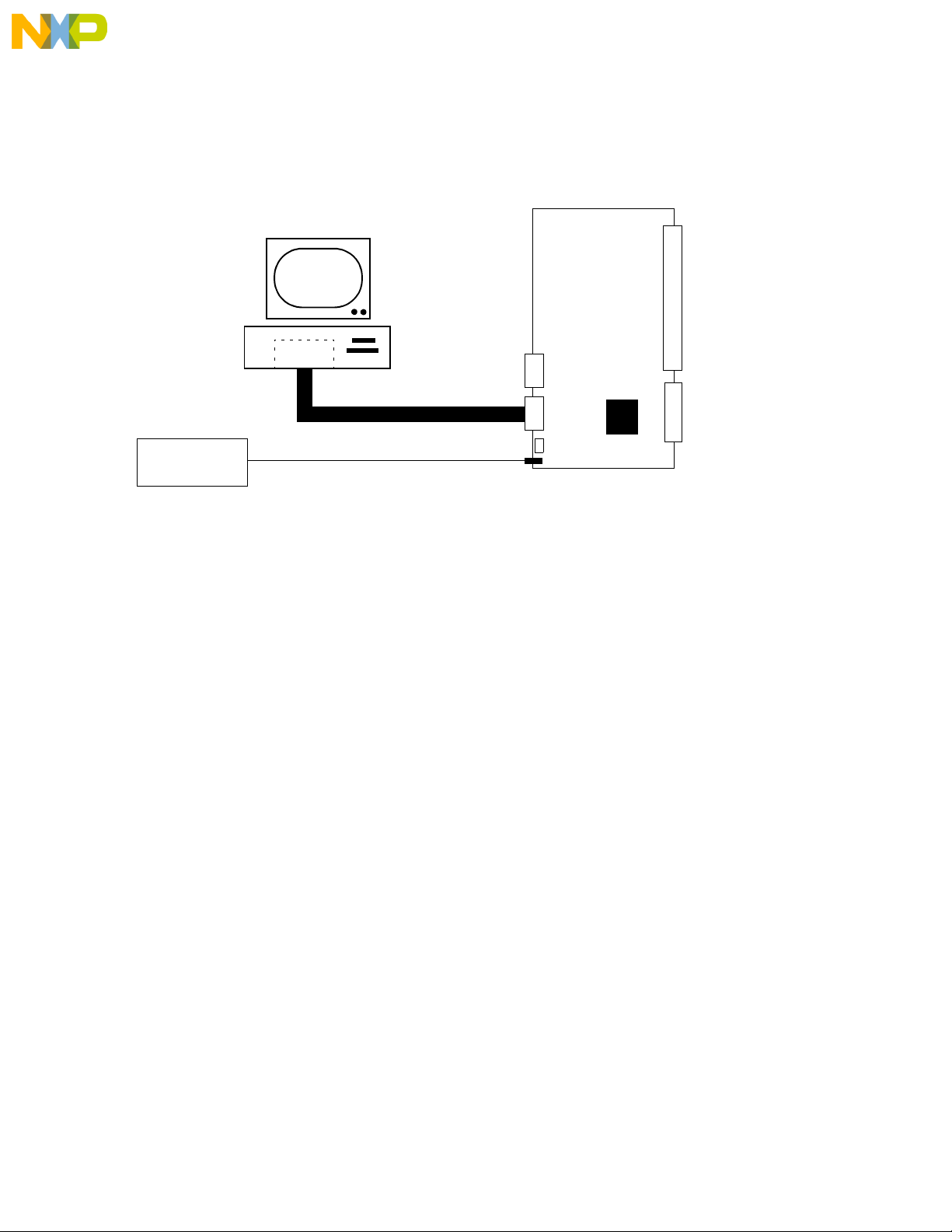
2.3.2 Connecting M68VZ328ADS to PC
Figure 2-6 shows connections among the PC, the external power supply and the
M68VZ328ADS board. Use the following steps to complete cable connections:
Host Computer
COM1
/COM2
RS232 Cable
3.0-3.3V
Power Supply
UART2
UART1
M68VZ328ADS
Figure 2-6. Connecting PC to UART1 of M68VZ328ADS
For m ost evaluation platforms, serial communication is the primary channel to link up PC
withthe target board.Both Microtek (SLD)and SoftwareDevelopment System (SDS)debug
monitor support serial communication through UART port. The procedure are as follows.
1. Connect a RS232 cable from COM port (COM1 or COM2) to connector P2 of
M68VZ328ADS.
2. Connect the power supply +3V or power adaptor to the P1 of M68VZ328ADS
3. Turn on the power supply. The RED LED will flash and the GREEN LED will illuminate
when power is correctly applied.
Freescale Semiconductor, I
2.3.3 Installing software debugger
The following software debugger supports M68VZ328ADS:
• Metrowerks Codewarrior
• Single Step Development System
•SLD
Metrowerks Codewarrior
A simple procedure for using Metrowerks Codewarrior Target Monitor:
1. Install the Metrowerks Codewarrior IDE
2-12 M68VZ328ADS USER’S MANUAL MOTOROLA
For More Information On This Product,
Go to: www.freescale.com
Page 13
nc...
Quick Installation Guide
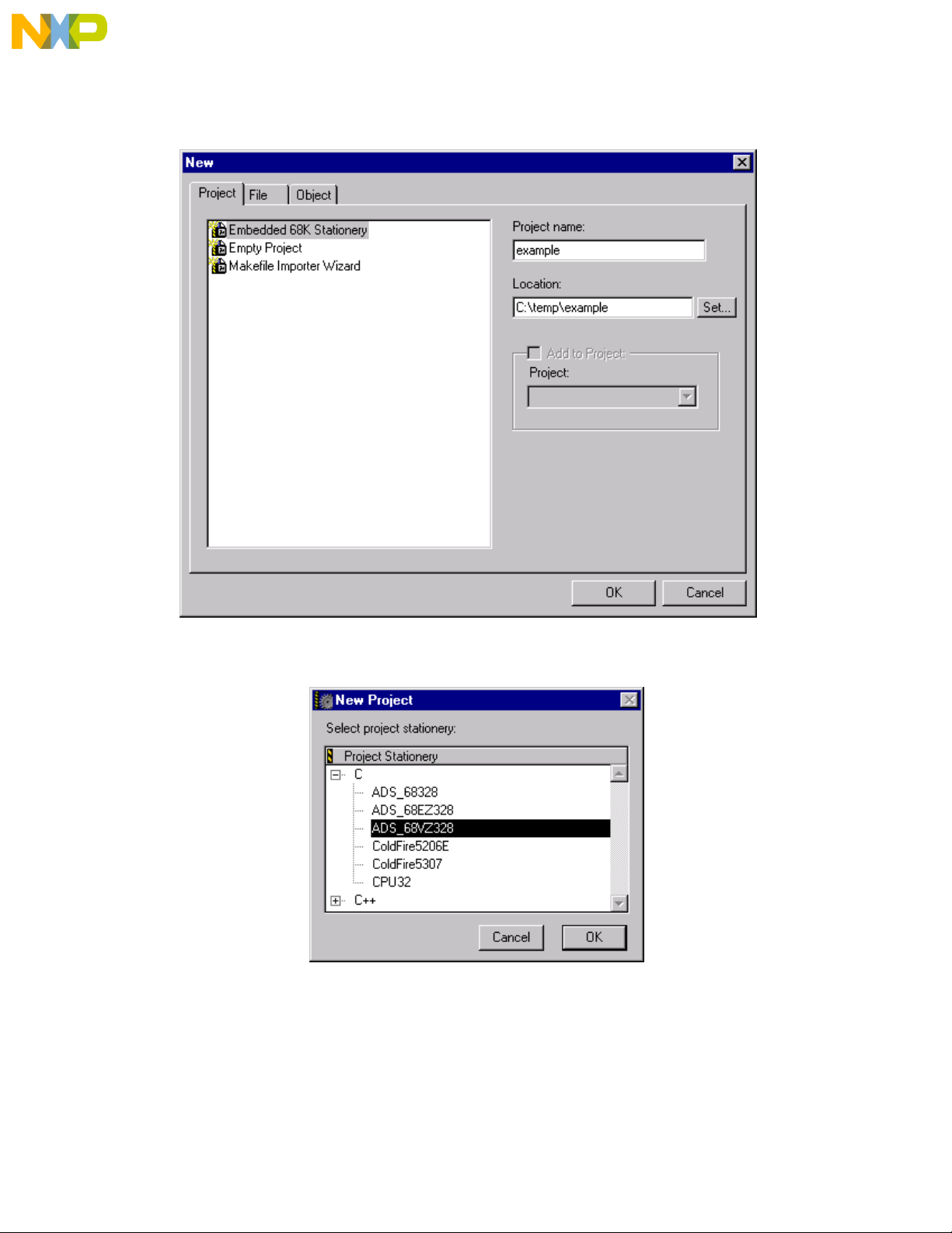
2. Run Codewarrior IDE program.
3. Open a new project file with Embedded 68k Stationery.
Freescale Semiconductor, Inc.
4. Select ADS_68VZ328 Stationery for new project.
Freescale Semiconductor, I
2-13 M68VZ328ADS USER’S MANUAL MOTOROLA
For More Information On This Product,
Go to: www.freescale.com
Page 14
nc...
Quick Installation Guide
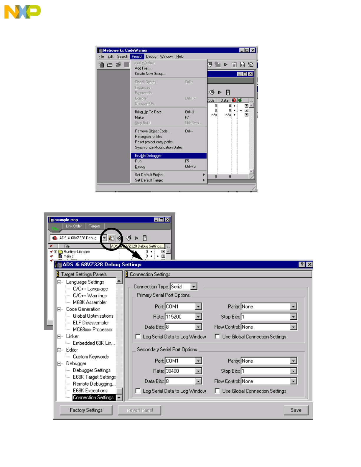
5. Choose "Enable Debugger" from the "Project" pull-down menu.
Freescale Semiconductor, Inc.
6. Change the connection settings in the Debug Settings Windows.
Freescale Semiconductor, I
2-14 M68VZ328ADS USER’S MANUAL MOTOROLA
For More Information On This Product,
Go to: www.freescale.com
Page 15
nc...
Quick Installation Guide
7. Edit the code inside the Codewarrior IDE program.
8. Press F5 to run the program.
Single Step Development System
A simple procedure for using Single Step Debugger:
1. Install the Single Step Debugger on your PC.
2. Run Single Step Debuger
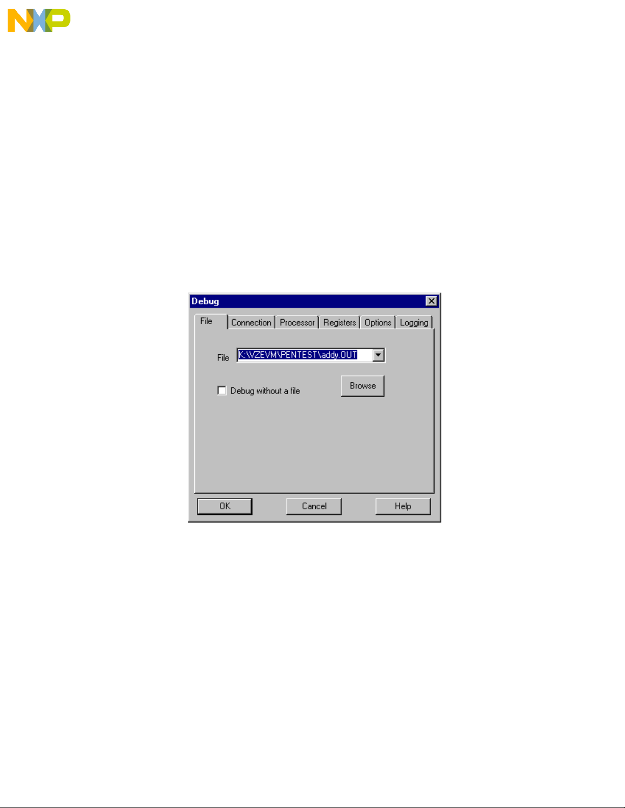
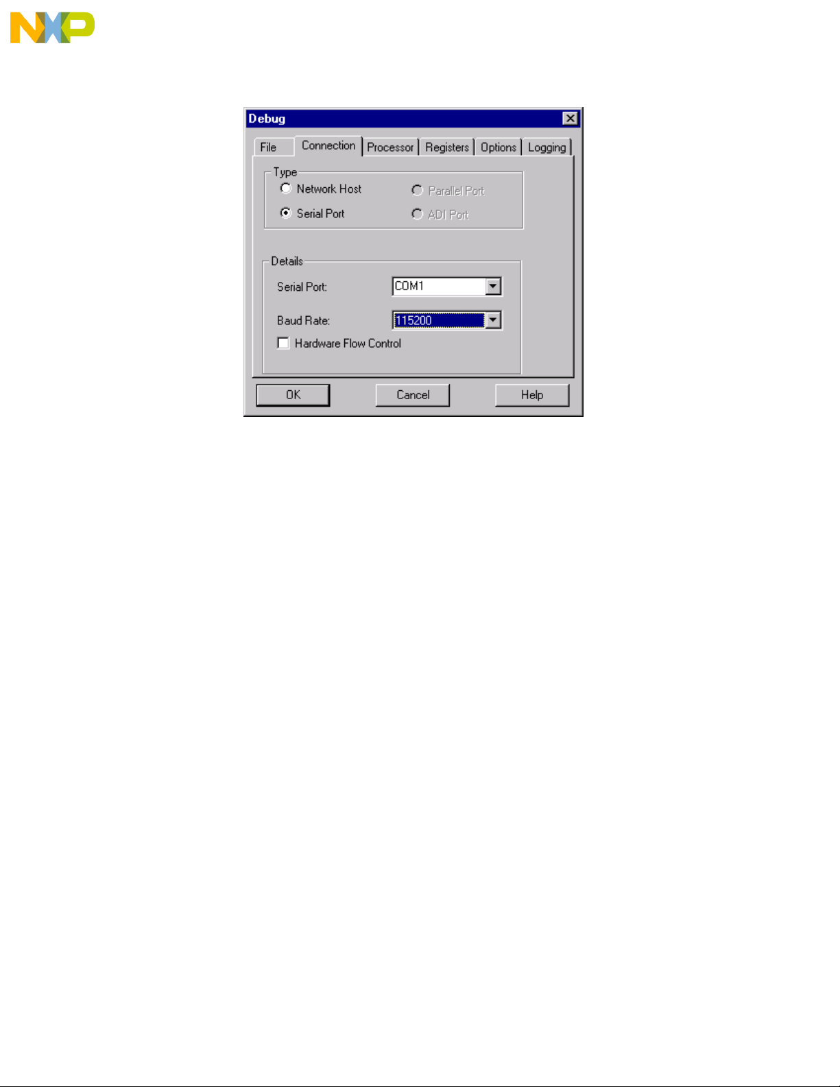
3. Choose Debug in the File pull-downmenutoopentheDebug pop-up window.
4. InsidetheDebug pop-upwindow,choose theobjectfile todownloador "debugwithout
file" asshownin Figure 2-7, select the serial port(COM1 or COM2 ...) accordingto the
serial port of the PC connecting to the ADS, disable "hardware flow control" and the
baud rate should be 115200bps as shown in Figure 2-8.
5. The fileshould be downloadedand then you can start your development. (For details,
please refer to the SingleStep User’s Manual).
Freescale Semiconductor, Inc.
Figure 2-7. Debug Pop-Up Window of SDS v7.4
Freescale Semiconductor, I
2-15 M68VZ328ADS USER’S MANUAL MOTOROLA
For More Information On This Product,
Go to: www.freescale.com
Page 16
nc...
Quick Installation Guide
Freescale Semiconductor, Inc.
Figure 2-8. Connection Setting inside Debug Pop-up Window of SDS v7.4
Freescale Semiconductor, I
2-16 M68VZ328ADS USER’S MANUAL MOTOROLA
For More Information On This Product,
Go to: www.freescale.com
Page 17
Freescale Semiconductor, Inc.
SECTION 3
HARDWARE DESCRIPTION AND BOARD OPERATION
3.1 OVERVIEW
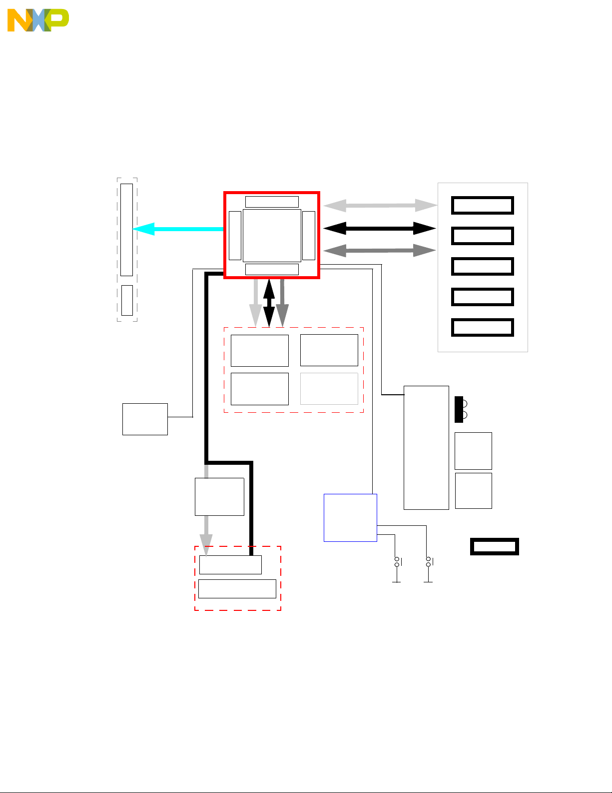
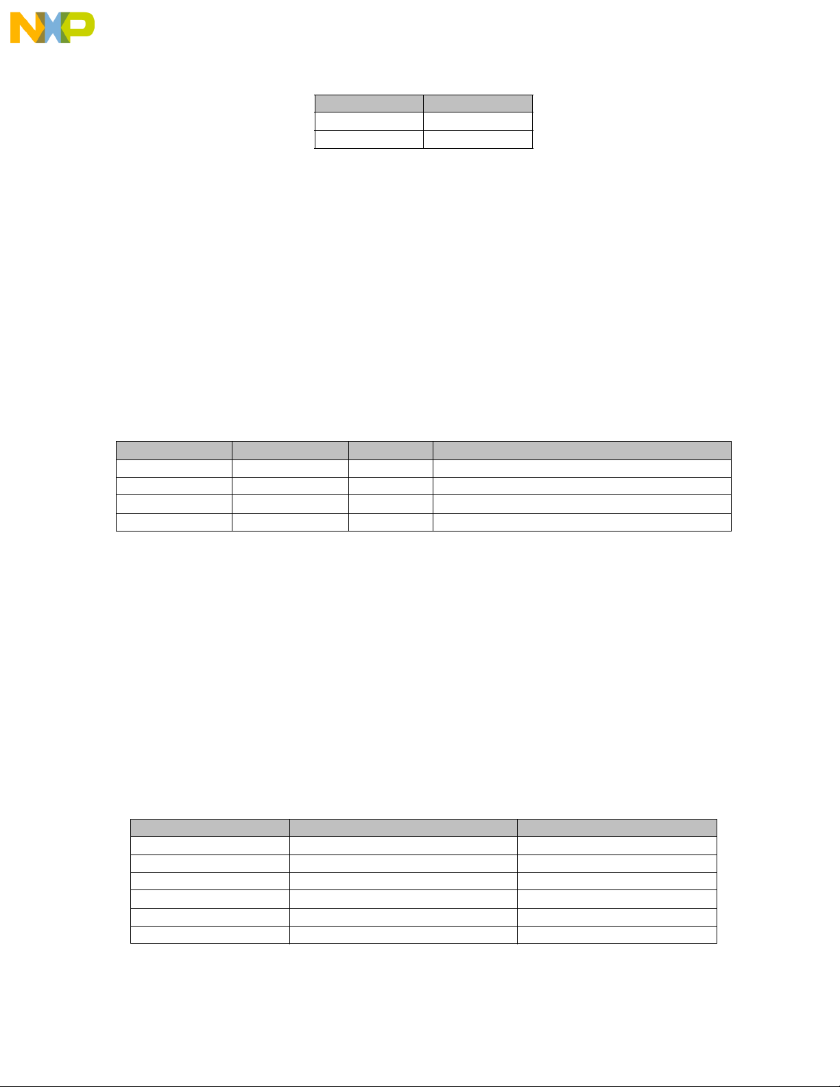
Figure 3-1shows the block diagram of M68VZ328ADS.
Logic Analyzer
nc...
Extension
Connectors
Single
Tone
Generator
PWMO
Touch
Panel
Controller
Extension
MC68VZ328
Connector
FLASH
1M x 16-bit
SDRAM
4M x 16-bit
UART SIGNALS
RESET
FLASH
1M x 16-bit
SDRAM
4M x 16-bit
Reset
Circuit
Address Bus
Data Bus
Control Bus
UART
and
IRDA
Interface
IRDA
UART1
UART2
Power
Connector
Freescale Semiconductor, I
4-bit LCD
8-bit LCD
LCD Connectors
Figure 3-1. M68VZ328ADS Functional Block Diagram
MOTOROLA M68VZ328ADS USER’S MANUAL 3-17
For More Information On This Product,
Go to: www.freescale.com
RESET
GND
ABORT
GND
Page 18
Hardware Description and Board Operation
Freescale Semiconductor, Inc.
3.2 CONTROL SWITCHES
There are two push buttons on the ADS which function as follows:
1. Reset Switch (SW2): When pressed, a hardware reset is generated to the
MC68VZ328 processor and resumes operation.
2. Abort Switch (SW1): This switch is used to generate a level 7 interrupt to the
MC68VZ328 processor for aborting normal software execution and returning control
to the debug monitor.
3.3 DIP SWITCHES
There are two DIP switch packs on the ADS board, S1 and S2. S1 is used to configure the
memory system and operation modes. S2 is used to enable the on-board peripheral such
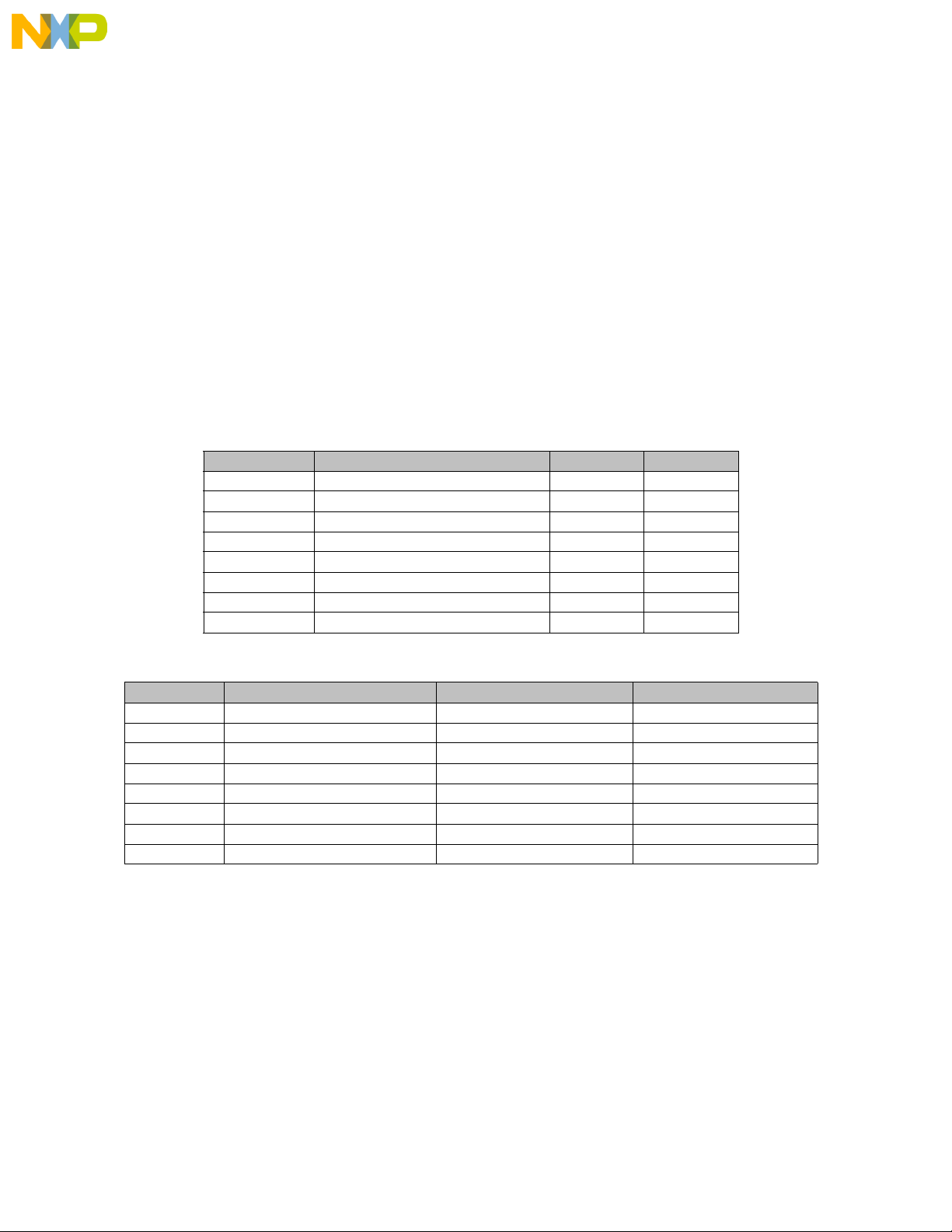
as buzzer and touch panel controller. Table 3-1 and Table 3-2 show the description of each
switch.
nc...
Switch FUNCTION ON OFF
S1-1 UART1 Transceiver Enable Disable
S1-2 UART2 Transceiver Enable Disable
S1-3 IRDA Module Enable Disable
S1-4 Buzzer Enable Disable
S1-5 Chip Select of Pen Input Enable Disable
S1-6 Pen IRQ Enable Disable
S1-7 Unused
S1-8 Unused
Table 3-1. DIP Switch pack S1 Setting
Table 3-2. DIP Switch pack S2 Setting
Switch FUNCTION ON OFF
S2-1 CSA0 - FLASH0 Connected Disconnected
S2-2 CSA0 - FLASH1 Connected Disconnected
S2-3 CSA1 - FLASH1 Connected Disconnected
S2-4 CSD0 - SDRAM0 Connected Disconnected
S2-5 CSD1 - SDRAM1 Connected Disconnected
S2-6 PD2 Low (UART2*) High (UART1*)
S2-7 PD3 Low (SDS monitor*) High (Metrowerks monitor*)
Freescale Semiconductor, I
S2-8 Bootstrap Mode Enable Disable
* Used as monitor and debug port selection in provided monitor program
3.4 OPERATION MODES
M68VZ328ADS supports two operation modes of MC68VZ328: Normal Mode and Bootstrap Mode. Selection of those operation modes is controlled by setting DIP switch S2-8.
Operation mode has to be selected before resetting the system. Mode is not allowed to be
changed during normal runing. Table 3-3 shows the operation mode configuration.
Normal mode - After power up or system reset in this mode, CSA0 is default to cover the
whole memory map except MC68VZ328 internal registers and EMU space. Also, as reset
3-18 M68VZ328ADS USER’S MANUAL MOTOROLA
For More Information On This Product,
Go to: www.freescale.com
Page 19
nc...
Freescale Semiconductor, Inc.
Hardware Description and Board Operation
Table 3-3. Operation Mode Setting
DIP Switch S2-8 Operation Mode
ON Bootstrap
OFF Normal
vector fetch is at the beginning of CSA0 space, *CSA0 should be connected to the boot
ROM in which the first two words are reset vectors. The default boot ROM of the
M68VZ328ADS has been programmed with monitor when it is shipped out from factory. Pls.
refer to Quick Installation part for detailed description on the selection of monitor and debug
port.
Bootstrap mode - When this mode is selected, the DragonBall-VZ will start its embedded
bootloader. User can use this mode to do simple debugging or reprogram the flash memories. For detailed bootstrap mode operation, please refer MC68VZ328 user’s manual.
3.5 LED INDICATORS
There are four LED indicators on the ADS which function as shown in Table 3-4.
Table 3-4. Function of LED Indicators
Reference # Color Name Function
LED1 Yellow PD0 Status of PD0
LED2 Yellow PD1 Status of PD1
LED3 Red Heart Beat Blinking heart beat indicates the system is "alive"
LED4 Green Power Power is applied to the system with right polarity
The LED3 is connected to a counter. The counter is toggled by address line A1.
3.6 MEMORY
M68VZ328ADS provides on-board Flash memory and SDRAM, for application development. They can be enabled or disabled individually by setting the corresponding DIP
switches.
3.6.1 Memory Map
The defaultmemory map of M68VZ328ADSin normal mode is shownin Table 3-5. The chip
Freescale Semiconductor, I
select range to all of the memory are software programmable. Users can reconfigure the
memory map for their applications.
Table 3-5. M68VZ328ADS Default Memory Map
System Address Memory Assigned Chip Select
$00000000-$007FFFFF 8MB SDRAM BANK0 CSD0
$00800000-$00FFFFFF 8MB SDRAM BANK1 (not installed) CSD1
$01000000-$011FFFFF 2MB FLASH BANK0 CSA0
$01200000-$013FFFFF 2MB FLASH BANK1 CSA1
$01400000-$FFFFEFFF Unused -
$FFFFF000-$FFFFFFFF MC68VZ328 Internal Register -
MOTOROLA M68VZ328ADS USER’S MANUAL 3-19
For More Information On This Product,
Go to: www.freescale.com
Page 20
Hardware Description and Board Operation
Freescale Semiconductor, Inc.
3.6.2 FLASH Memory
MC68VZ328
VCC VCC
nc...
1MX16-Bit FLASH
1MX16-Bit FLASH
FLASH1
FLASH0
CSA1
CSA0
A[1..20]
D[0..15]
OE
WE
S2-3
S2-2
S2-1
CE
CE
A[0..19]
D[0..15]
OE
WE
Figure 3-2. Interface of Flash Memories
M68VZ328ADS is equipped with two 2M-byte Flash memory chips. Figure 3-2. shows the
interface of them. They are chip-selected by *CSA0 and *CSA1 signals. The connection of
these *CSAx signals to the Flash memories is controlled by DIP switches S2-1, S2-2 and
S2-3.
When S2-1 and S2-3 are close, *CSA0 connects Flash0 and *CSA1 connects Flash1.
Flash0 becomes the boot ROM. When S2-1 and S2-3 are open and S2-2 is close, *CSA0
connects Flash1 only. Flash1 will then be boot ROM instead. So, user can select either
FLASH0 or FLASH1 to be the boot ROM. These configuration allow users to put their application program to boot ROM without having to erase the on-board monitor program.
Table 3-6 summaries the possible configuration of the S2-1, S2-2 and S2-3.
Freescale Semiconductor, I
Table 3-6. Possible Configuration of FLASH Memories
S2-1 S2-2 S2-3 Boot ROM Data ROM
ON OFF ON FLASH0 (Monitor Program) FLASH1
ON OFF OFF FLASH0 (Monitor Program) None
OFF ON OFF FLASH1 (User Progam) None
OFF OFF OFF None None
For more details on flash memory programming, please refer to Appendix B .
3-20 M68VZ328ADS USER’S MANUAL MOTOROLA
For More Information On This Product,
Go to: www.freescale.com
Page 21
3.6.3 SDRAM
Freescale Semiconductor, Inc.
Hardware Description and Board Operation
nc...
MC68VZ328
VCC
S2-5
CSD1
S2-4
CSD0
SDCE
SDCLK
CSC0
CSC1
DQMH
DQML
SDWE
A[1..20]
D[0..15]
VCC
CS
CKE
CLK
RAS
CAS
UDQM
LDQM
WE
A[1..12], BS0,BS1
D[0..15]
Figure 3-3. Interface of SDRAMs
4MX16-Bit SDRAM
CS
4MX16-Bit SDRAM
SDRAM1
SDRAM0
Figure 3-3. shows the interface of SDRAMs. M68VZ328ADS supports two banks of 4Mx16bit SDRAMs. However, only one bank is installed when the board is shipped out from the
factory. This allows user to install and test their own SDRAM when needed. These two
banks of SDRAM are selected by *CSD0 and *CSD1, and enabled by closing DIP switches
S2-4 and S2-5.
Freescale Semiconductor, I
MOTOROLA M68VZ328ADS USER’S MANUAL 3-21
For More Information On This Product,
Go to: www.freescale.com
Page 22

Hardware Description and Board Operation
Freescale Semiconductor, Inc.
3.7 UART AND IRDA
MC68VZ328
TXD1
RXD1
RTS1
CTS1
RS232 Transceiver
EN
P2
UART1
VCC
nc...
TXD2
RXD2
RTS2
CTS2
PD4
S1-3
VCC
RS232 Transceiver
EN
Buffer
EN
EN
P3
UART2
IRDA
GND
S1-1
VCC
S1-2
GND
Figure 3-4. UART and IRDA Interface.
Figure 3-4 shows the UART and IRDA interface. The M68VZ328 has two RS232 serial
ports, P2 and P3. P2 and P3 are using the UART1andUART2 of MC68VZ328 respectively.
BothP2andP3are9-pinfemaleD-TypeconnectorscontainingthesignalsasshowninFigure 3-5. The transceivers for UART1 and UART2 can be enabled by turning the DIP switch
S1-1 and S1-2 on respectively.
NC
Freescale Semiconductor, I
TXD
RXD
NC
GND
Figure 3-5. Serial Port Pin Assignment
The IRDA transceiver is connected to UART2 only with a buffer in between for controlling
its ON/OFF. If IRDA is being used, S1-2 should be switched OFF and S1-3 should be
3-22 M68VZ328ADS USER’S MANUAL MOTOROLA
For More Information On This Product,
Go to: www.freescale.com
1
2
3
4
5
NC
6
CTS
7
RTS
8
NC
9
Page 23

Freescale Semiconductor, Inc.
Hardware Description and Board Operation
switchedON. Then, the enable/disableof IRDA istotally controlled bysoftware through PD4
(Port D4).
3.8 LCD AND TOUCH PANEL INTERFACE
3.8.1 LCD Interface
M68VZ328ADS consists of two LCD panel connectors, P1 and P12. P12 is designed for 8bit LCD panel while P1 is for 4-bit LCD panel. P1 is fully compatible with the one used on
M68EZ328ADS. The pin assignments of both LCD connectors are shown in Figure 3-6.
nc...
LACD
LLP
VO
GND
LD0
LD2
GND
NC
TOP
LEFT
P1
1
3
5
7
9
11
13
15
17
19
2
LFRM
4
LCLK
6
VCC
8
VEE
10
LD1
12
LD3
14
LCONTRAST
16
NC
18
BOTTOM
20
RIGHT
LCONTRAST
LACD
LLP
VO
GND
LD0
LD2
LD4
LD6
NC
TOP
LEFT
NC
P12
1
3
5
7
9
11
13
15
17
19
21
23
25
2
4
6
8
10
12
14
16
18
20
22
24
26
LD5
LD7
NC
RIGHT
NC
LFRM
LCLK
VCC
VEE
LD1
LD3
NC
BOTTOM
Figure 3-6. LCD and Touch Panel Connector Pin Assignment
For full description of the LCD signals, please refer to the MC68VZ328 User’s Manual.
Freescale Semiconductor, I
MOTOROLA M68VZ328ADS USER’S MANUAL 3-23
For More Information On This Product,
Go to: www.freescale.com
Page 24

Hardware Description and Board Operation
Freescale Semiconductor, Inc.
3.8.2 Touch Panel Interface
nc...
RIGHT
TOP
LEFT
BOTTOM
MC68VZ328
PB6
IRQ5
SPMCLK
SPMTXD
SPMRXD
S1-6
S1-5
Touch Panel
VCC
ADS7843
CS
PENIRQ
DCLK
DIN
DOUT
Figure 3-7. Touch Panel Controller Interface
The VZADS boardis equipped with Burr-Brown TouchPanelController ADS7843. Figure37shows the interface of Touch Panel Controller. Totally one I/O signal,oneinterrupt capable
I/O signal and one set of SPIM signals from MC68VZ328 are used to implement the touch
panel circuitry. All of these signals can be shared for other devices when touch panel interface controller is being disabled. The on-board touch panel controller can be disabled by
turningbothDIPswitchesS1-5,S1-6off.
Table 3-7. Signal Assignment for Touch Panel Controller
Signals Function
This set of serial port interface signals performs data transfer with
SPMRXD, SPMTXD, SPMCLK
~IRQ5 This signal is driven from an MC68VZ328 interrupt capable I/O pin.
PB6
Freescale Semiconductor, I
The ADS7843 is a 12-bit sampling analog-to-digital converter (ADC) with a synchronous
ADS7843. For detailed operation on the SPI port, please refer to the
The MC68VZ328 general I/O signal is used to select the ADS7843 on data
serial interface and low on-resistance switches for driving touch screens. The ADS7843
communicates with MC68VZ328 through SPI (Serial Peripheral Interface). In this case,
ADS7843isslave, and MC68VZ328 is master.Forthe details on the operation ofADS7843,
please refer to i ts datasheet. The datasheet is available on the web:
http://www.burr-brown.com
For more details on the operation of resistive touch panel, please refer to Appendix A .
MC68VZ328 User’s Manual.
transfer.
3-24 M68VZ328ADS USER’S MANUAL MOTOROLA
For More Information On This Product,
Go to: www.freescale.com
Page 25

Freescale Semiconductor, Inc.
3.9 SINGLE TONE GENERATOR
S1-4
PWMO
MC68VZ328
Figure 3-8. Single Tone Generator
Hardware Description and Board Operation
VCC
BC847
CitiSound CHB-03E
GND
nc...
The M68VZ328ADS is equipped with Citizen single tone generator CHB-03E. As shown in
Figure 3-8, a simple transistor circuit is used to interface the CHB-03E with the PWMO pin
of MC68VZ328.
3.10 LOGIC ANALYZER INTERFACE
Toprovide an convenientway ofconnecting on-boardsignalsto a logicanalyzer, ADSboard
provides five 10x2-pin headers for direct plug-in. Pin assignments to these five headers are
showninFigure3-9.
POD3
2
1
3
5
7
9
11
13
15
17
19
4
6
8
10
12
14
16
18
20
DTACK
D15
D13
D11
D9
D7
D5
D3
D1
GND
A14
A12
A10
A8
A6
A4
A2
A0
EMUCS
RSTIN
EMUCS
LWE
CONTRAST
LCLK
LFRM
POD4
2
1
4
3
6
5
8
7
10
9
12
11
14
13
16
15
18
17
20
19
CLKO
D14
D12
D10
D8
D6
D4
D2
D0
Freescale Semiconductor, I
LD2
LD0
A15
A13
A11
A9
A7
A5
A3
A1
GND
POD2
1
3
5
7
9
11
13
15
17
19
2
4
6
8
10
12
14
16
18
20
EMUIRQ
OE
UWE
DTACK
LACD
LLP
LD3
LD1
GND
LD6
LD4
UDS
DWE
SDA10
DQMH
SDCLK
POD5
1
3
5
7
9
11
13
15
17
19
CSA0
CSA1
CSB1
RAS1
CAS1
A22
A20
A18
A16
2
4
6
8
10
12
14
16
18
20
POD1
1
3
5
7
9
11
13
15
17
19
LD7
LD5
WE
LDS
DMOE
DQML
SDCE
GND
10
12
14
16
18
20
2
4
6
8
CSA0
CSB0
RAS0
CAS0
A23
A21
A19
A17
GND
Figure 3-9. Logic Analyzer Connectors
MOTOROLA M68VZ328ADS USER’S MANUAL 3-25
For More Information On This Product,
Go to: www.freescale.com
Page 26

Hardware Description and Board Operation
Freescale Semiconductor, Inc.
3.11 EXPANSION CONNECTORS
The M68VZ328ADS provides basic features for software development and evaluation. If
user wants to add application subsystem to M68VZ328ADS, it can utililize the signals provided on 32x3 local bus connector (P7) and 16x3 local bus connector (P9). Some of these
MC68VZ328 signals are used by the on-board modules. If users want to use any of these
signalsfor their daughtercard, the correspondingon-board modulemayhave to be disabled
to avoid contention. Pin assignment on P7 is compatible with the one used on
M68EZ328ADS. Any daughter card used on M68EZ328ADS can also be used on
M68VZ328ADS.
The pin assignments for extension connectors are shown in Table 3-8 and Table 3-9.
Table 3-8. Pin Assignments of P7
Pin# A B C
1 GND GND GND
nc...
Freescale Semiconductor, I
2 D0/PA0 D1/PA1 D2/PA2
3 D3/PA3 D4/PA4 D5/PA5
4 D6/PA6 D7/PA7 D8
5 D9 D10 D11
6 D12 D13 D14
7 D15 CSA0 PF7/CSA1
8 PB0/CSB0 PB1/CSB1/SDWE PB2/CSC0/RAS0
9 PB3/CSC1/RAS1 PB4/CSD0/CAS0 PB5/CSD1/CAS1
10 PB6/TOUT/TIN PB7/PWMO1 PC0/LD0
11 PC1/LD1 PC2/LD2 PC3/LD3
12 PC4/LFRM PC5/LLP PC6/LCLK
13 PC7/LACD PD0/INT0 PD1/INT1
14 PD2/INT2 PD3/INT3 PD4/IRQ1
15 PD5/IRQ2 PD6/IRQ3 PD7/IRQ6
16 PE0/SPMTXD PE1/SPMRXD PE2/SPMCLK
17 PE3/DWE/UCLK PE4/RXD1 PE5/TXD1
18 PE6/RTS1 PE7/CTS1 PF0/LCONTRAST
19 PF1/IRQ5 PF2/CLKO PG1/A0
20 MA0/A1 MA1/A2 MA2/A3
21 MA3/A4 MA4/A5 MA5/A6
22 MA6/A7 MA7/A8 MA8/A9
23 MA9/A10 MA10/A11 MA11/A12
24 MA12/A13 MA13/A14 MA14/A15
25 MA15/A16 A17 A18
26 A19 PF3/A20 PF4/A21
27 PF5/A22 PF6/A23 PG2/EMUIRQ
28 PG3/HIZ/P/D PG4/EMUCS PG5/EMUBRK
29 PG0/BUSW/DTACK RESET OE
30 UWE/UB LWE/LB PK2/LDS
31 PK3/UDS PK1/R/W NC
32 VCC VCC VCC
3-26 M68VZ328ADS USER’S MANUAL MOTOROLA
For More Information On This Product,
Go to: www.freescale.com
Page 27

nc...
Freescale Semiconductor, Inc.
Hardware Description and Board Operation
Table 3-9. Pin Assignment of P9
Pin# A B C
1 GND GND GND
2 PM0/SDCLK PM1/SDCE PM2/DQMH
3 PM3/DQML PM4/SDA10 PM5/DMOE
4 PK4/LD4 PK5/LD5 PK6/LD6
5 PK7/LD7 RXD2 TXD2
6 RTS2 CTS2 MOSI
7 MISO SPICLK SS
8 SPIRDY NC NC
9 NC NC NC
10 NC NC NC
11 NC NC NC
12 NC NC NC
13 NC NC NC
14 NC NC NC
15 NC NC NC
16 VCC VCC VCC
3.12 POWER SUPPLY
There are two power input connectors on the ADS, P4 and P5. P4 is designed for external
3V DC main power supply, which supplies power to the MC68VZ328 processor and most of
the on-board components. P5 is used for LCD driver (VEE) power supply. If an LCD panel
is connected to the ADS, the LCD driver can be powered by this VEE input. Figure 3-10
locates the power connectors and their polarity.
P5
GND
VEE
Freescale Semiconductor, I
P4
GND
_
3.0-3.3V
+
UART2
UART1
M68VZ328ADS
Figure 3-10. Power Connectors
MOTOROLA M68VZ328ADS USER’S MANUAL 3-27
For More Information On This Product,
Go to: www.freescale.com
Page 28

nc...
Hardware Description and Board Operation
Freescale Semiconductor, Inc.
Freescale Semiconductor, I
3-28 M68VZ328ADS USER’S MANUAL MOTOROLA
For More Information On This Product,
Go to: www.freescale.com
Page 29

nc...
Freescale Semiconductor, Inc.
APPENDIX A
RESISTIVE TOUCH PANEL OPERATION
M68EZ328ADSfeatures pen input through a resistive-film sensing panel. This type of panel
provides high flexibility by accepting input form any kind of stimulus including fingers, which
is most suitable for portable use. User can select a specific touch panel or order an LCD
module which includes a touch resistive panel. This section describes the basic concepts of
pen input and the required interface with the M68EZ328ADS.
A.1 GENERAL CONCEPTS OF RESISTIVE PANELS
Basically, resistive panel consists of two transparent resistive layers separated by insulating
spacers as shown in Figure 1-1.
Figure 1-1. Resistive Touch Panel
Freescale Semiconductor, I
Transparent Resistive Layer
coated on dielectric (insulating) substrate, usually glass on bottom and plastic on top for
actuation.
Bars
- highly conductivematerial such as silver ink, about1000 timesmore conductive than
ITO.
Spacers
the two opposite conductive layers.
MOTOROLA M68VZ328ADS USER’S MANUAL A-29
- Non-conductingink,adhesive, orother materialsuch as Mylaris used to separate
- resistive material such as an indium tin oxide (ITO) film is
For More Information On This Product,
Go to: www.freescale.com
Page 30

nc...
Resistive Touch Panel Operation
The resistive panel works by applying a voltage gradient across one conductive layer and
measuring the voltage at the point of contact with the opposing conductive layer. For
instance, as shown in Figure 1-2, the resistive film acts as a series of resistors.
Freescale Semiconductor, Inc.
Figure 1-2. Determination of X,Y Position
When a point is contacted, it means the two opposing conductive layers come into electrical
contact. The x position of actuation can be determined by measuring the output voltage of
the y layer. At the same time, the y position can be find out by measuring the x layer. The
exact position can be determined by referencing the output voltage to the distance relationship.
Freescale Semiconductor, I
A-30 M68VZ328ADS USER’S MANUAL MOTOROLA
For More Information On This Product,
Go to: www.freescale.com
Page 31

Freescale Semiconductor, Inc.
APPENDIX B
PROGRAMMING ON-BOARD FLASH MEMORY
B.1 OVERVIEW
The Flash memory on the ADS board cannot be written directly. A special program command sequence is required to unlock it before starting the write process. A flash program is
thereforeprovided withthe ADS board forhelping users todo re-programming.The sections
below will describe the program and provide further information about the process and other
required elements.
Itis recommendedthat usershould have abasic understandingof bootstrapmode operation
of MC68VZ328 before reading the material below. For more details on Bootstrap mode,
please refer to the MC68VZ328 user’s manual.
nc...
B.2 ELEMENTS FOR PROGRAMMING THE FLASH
The following files are necessary for programming the Flash memory
1. VZTOOLS including BBUGV.EXE and STOB.EXE
2. INIT.B - b-record for initialize the ADS
3. ERASE.B - b-record for erasing Flash memory
4. FLASH.B - b-record for programming flash. ROM image is copied from RAM area to
the Flash memory area
5. ROM.B - ROM image of user program in b-record/s-record format.
Freescale Semiconductor, I
MOTOROLA M68VZ328ADS USER’S MANUAL B-31
For More Information On This Product,
Go to: www.freescale.com
Page 32

Programming On-board Flash Memory
Freescale Semiconductor, Inc.
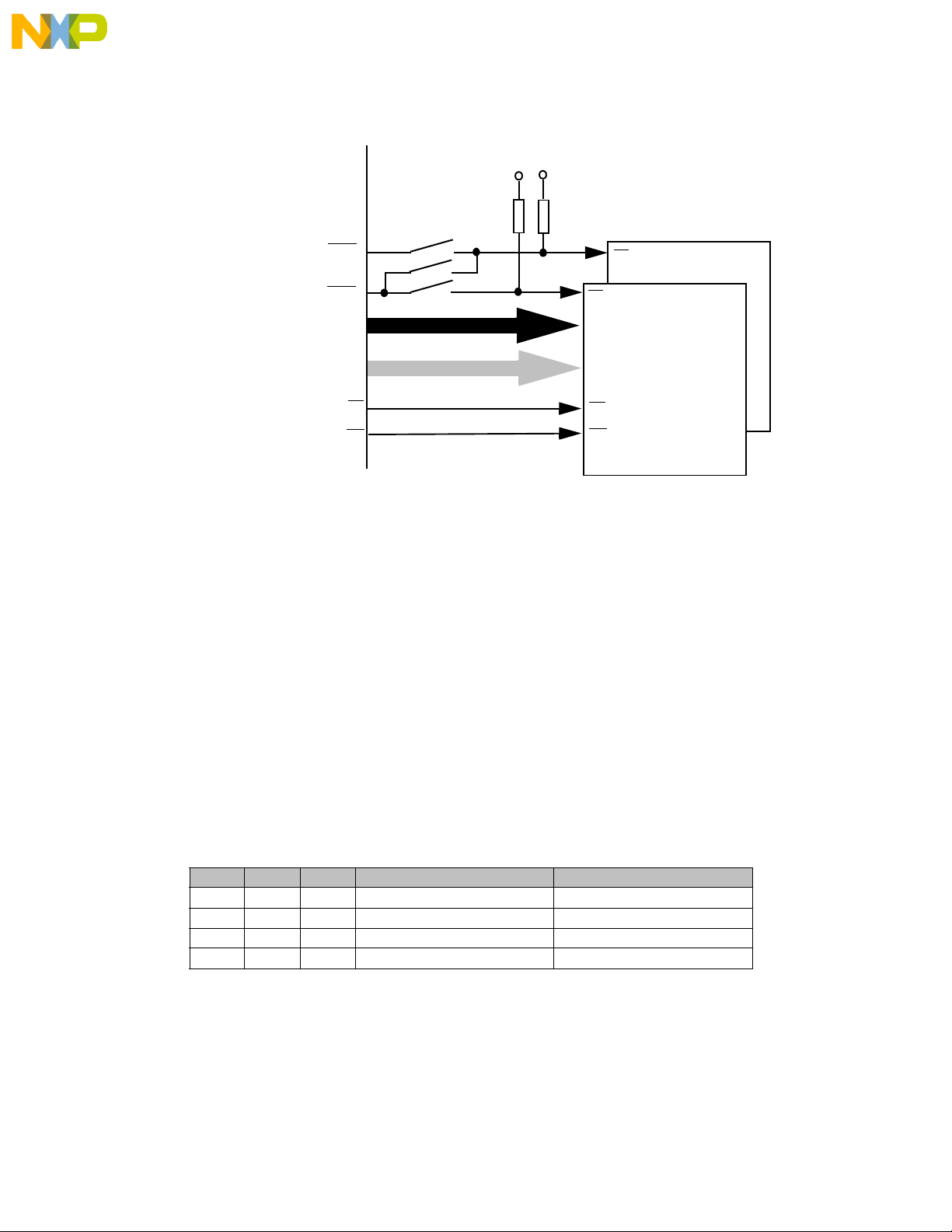
B.3 METHOD
System RAM
FLASH Program
nc...
ROM Image
offset
Copy the ROM Image from
system RAM to Flash
Memory by the flash Program.
Flash Memory
Figure B-1. Method of programming on-board Flash memory
Flash memory can be programmed in bootstrap mode. First, a ROM image and a flash program are downloaded to the system memory by loading their b-records. Then, run the flash
program. It will execute the Flash program command sequence and copy the ROM image
from the system RAM to the Flash memory. The detailed steps are as follows.
1. Force the MC68VZ328 into bootstrap mode by turning S2-8 on and pressing RESET
switch once.
2. Use BBUGV.EXE or TERMINAL program to communicate with the M68VZ328ADS
through RS232 port of a PC.
3. Initialize the internal registers of DragonBall-VZ by loading the INIT.B.
4. Make sure the Flash Memory is blank. Load ERASE.B to erase the flash memory
when needed.
Freescale Semiconductor, I
5. Load FLASH.B (the Flash Program) and ROM.B (the ROM image) to system RAM
(SDRAM on M68VZ328ADS).
6. Executethe Flash Program by using the execution B-record. For example, if the startingaddress ofFlash Programis 0x4000,the executionB-recordis then"0000400000".
B.4 OFFSET ADDRESS OF ROM IMAGE
FigureB-1The ROM imageisfirst put tothe system RAM beforeit is copiedto Flash. In order
to create S-record/B-record with download address different from its execution address, an
OFFSET is sometimes required to b e specified in downloader program.
B-32 M68VZ328ADS USER’S MANUAL MOTOROLA
For More Information On This Product,
Go to: www.freescale.com
Page 33

Programming On-board Flash Memory
Freescale Semiconductor, Inc.
For example, when using SDS’s DOWN.EXE to generate the s-record, the "-w offset"
parameter can be used to specify this offset value. Please refer to the SingleStep User
Guide for using this command.
B.5 EXECUTING PROGRAM COMMAND SEQUENCE
Listed below is the source code of the flash Program which contains the neccessary steps
to write theflashmemory. It executes the flash program commandsequenceand copies the
ROM image from RAM area to the Flash memory area on ADS board. Figure B-2 shows the
flow chart of this p rogram. Different brands of Flash memory may have different program
command sequences, please refer to their datasheets for more details.
XREF STKTOP
OFFSET1 equ $AAA
OFFSET2 equ $554
nc...
Freescale Semiconductor, I
TIME equ $FFF
*****************************************************************
ECHO MACRO CHAR
bsr TXD_RDY
nop
nop
nop
move.b #CHAR,$FFFFF907
ENDM
*****************************************************************
ENABLE MACRO
move.w #$00AA,(A5) ; Unlock Flash
move.w #$0055,(A6)
move.w #$00A0,(A5)
ENDM
*****************************************************************
SECTION parameter
pSOURCE DC.L $00010000
pTARGET DC.L $01000000
pSIZE DC.L $00010000
pFLASH DC.L $01000000
pERROR DC.L $0
pFINISH DC.L $0
pERROR_ADDRESS DC.L $0
DC.L STKTOP
*****************************************************************
SECTION code
START
MOVEA.L #STKTOP,a7 ;re-istall stack pointer in case bootstrap mode
MOVE.L #0,pERROR
MOVE.L #0,pFINISH
move.l #0,pERROR_ADDRESS
B-33 M68VZ328ADS USER’S MANUAL MOTOROLA
For More Information On This Product,
Go to: www.freescale.com
Page 34

nc...
Programming On-board Flash Memory
move.l pSOURCE,A0
move.l pTARGET,A1
move.l pSIZE,D0
move.l pFLASH,A5
move.l pFLASH,A6
*******************************************
* BreakPoint Here if program flash in SDS *
*******************************************
add.l #OFFSET1,A5
add.l #OFFSET2,A6
**************************************************
;*****************************************
; Input Parameters:
; a0 - (Long) Source Address
; a1 - (Long) Target Address
; d0 - (Long) Byte Size
; a5 - (long) Flash Starting Address Offset1
; a6 - (long) Flash Starting Address Offset2
;*****************************************
Freescale Semiconductor, Inc.
move.l a0,a2 ; a2 as source
move.l a1,a3 ; a3 as target
clr.l d1 ; clear d1 as counter
clr.b d5 ; clear d5 as ECHO counter
PROGRAM
ENABLE
move.w (a2),(a3) ; Copy source to target
clr.l d4 ; clear d4 as polling counter
POLLING
cmp.l #TIME,d4
bgt ERROR ; if d4>#TIME, bra ERROR
add.l #1,d4 ; d4++
Freescale Semiconductor, I
NO_W add.b #1,d5
move.w (a2),d2 ; Compare (a0),(a1)
move.w (a3),d3
cmp.w d2,d3
bne POLLING ; End of POLLING
add.l #2,a2
add.l #2,a3
add.l #2,d1
cmp.b #0,d5
bne NO_W
ECHO 'W'
ECHO 0
B-34 M68VZ328ADS USER’S MANUAL MOTOROLA
For More Information On This Product,
Go to: www.freescale.com
Page 35

nc...
Programming On-board Flash Memory
cmp.l d0,d1 ; if d1<=d0, bra PROGRAM
ble PROGRAM
;*****************************************
; Input Parameters:
; a0 - (Long) Source Address
; a1 - (Long) Target Address
; d0 - (Long) Byte Size
; a5 - (long) Flash Starting Address Offset 1
; a6 - (long) Flash Starting Address Offset 2
;*****************************************
move.l a0,a2 ;a2 & a3 are used to store the starting address
move.l a1,a3 ;for comparing.
clr.b d5 ;clear d5 as ECHO counter
clr.l d1 ;clear d1 as counter
VERIFIY
cmp.b #0,d5
bne NO_V
ECHO 'V'
ECHO 0
NO_V add.b #1,d5
Freescale Semiconductor, Inc.
move.w (a2)+,d2
move.w (a3)+,d3
cmp.w d2,d3
bne ERROR
add.l #2,d1
cmp.l d0,d1 ; if d1<=d0, bra CHECK
ble VERIFIY
bra FINISH
****************************************************************************
TXD_RDY
move.l d7,-(a7) ; Push d7
POLLTXD
Freescale Semiconductor, I
LP_RDY sub.w #1,d7
btst.b #5,$FFFFF906
beq.s POLLTXD ; bra if TXAVAIL not SET
move.w #$0FFF,d7
bne.b LP_RDY
move.l (a7)+,d7 ; Restore d7
rts
****************************************************************************
FINISH
ECHO '\n'
ECHO 'P'
ECHO 'A'
B-35 M68VZ328ADS USER’S MANUAL MOTOROLA
For More Information On This Product,
Go to: www.freescale.com
Page 36

nc...
Programming On-board Flash Memory
ECHO 'S'
ECHO 'S'
ECHO '\n'
ECHO 0
ECHO 0
ECHO 0
ECHO 0
ECHO 0
ECHO 0
move.l #1,pFINISH
bra BOOTSTRAP
************************************************************
ERROR
ECHO '\n'
ECHO 'E'
ECHO 'R'
ECHO 'R'
ECHO 'O'
ECHO 'R'
ECHO '\n'
ECHO 0
ECHO 0
ECHO 0
ECHO 0
ECHO 0
ECHO 0
sub.l #1,a3
move.l a3,pERROR_ADDRESS
move.l #1,pERROR
bra BOOTSTRAP
Freescale Semiconductor, Inc.
************************************************************
BOOTSTRAP
jmp $FFFFFF5A
************************************************************
END
Freescale Semiconductor, I
B-36 M68VZ328ADS USER’S MANUAL MOTOROLA
For More Information On This Product,
Go to: www.freescale.com
Page 37

nc...
Programming On-board Flash Memory
Freescale Semiconductor, Inc.
Freescale Semiconductor, I
B-37 M68VZ328ADS USER’S MANUAL MOTOROLA
Figure B-2. Flash Program Algorithm
For More Information On This Product,
Go to: www.freescale.com
Page 38

nc...
Programming On-board Flash Memory
Freescale Semiconductor, Inc.
Freescale Semiconductor, I
B-38 M68VZ328ADS USER’S MANUAL MOTOROLA
For More Information On This Product,
Go to: www.freescale.com
Page 39

Freescale Semiconductor, Inc.
APPENDIX C
MONITOR INITIALIZATION CODE
C.1 INITIALIZATION CODE OF METROWERKS MONITOR (RESET.S)
;******************************************************************;
; This is the boot routine for the MC68VZ328 ADS board. Product
; engineers should examine all the configurations carefully and
; change them according to their system requirements.
;******************************************************************;
MON_BOOT .equ ___reset ; Boot entry point
MON_STACKTOP.equ$4100 ; Initial stack
M328BASE .equ $FFFFF000 ; Base address for system registers
; SIM28 System Configuration Registers
SCR .equ (M328BASE+$000)
; Chip Select Registers
nc...
Freescale Semiconductor, I
GRPBASEA .equ(M328BASE+$100)
GRPBASEB .equ(M328BASE+$102)
GRPBASEC .equ(M328BASE+$104)
GRPBASED .equ(M328BASE+$106)
CSA .equ (M328BASE+$110)
CSB .equ (M328BASE+$112)
CSC .equ (M328BASE+$114)
CSD .equ (M328BASE+$116)
CSCR .equ (M328BASE+$10A)
DRAMCFG .equ (M328BASE+$C00)
DRAMMC .equ (M328BASE+$C00)
DRAMCTL .equ (M328BASE+$C02)
DRAMC .equ (M328BASE+$C02)
SDCTRL .equ (M328BASE+$C04)
EMUCS .equ (M328BASE+$118)
CSCTR .equ (M328BASE+$150)
; PLL Registers
PLLCR .equ (M328BASE+$200); Control Reg
PLLFSR .equ (M328BASE+$202); Freq Select Reg
PLLTSR .equ (M328BASE+$204); Test Reg
; Power Control Registers
PCTLR .equ (M328BASE+$206); Control Reg
; Interrupt Registers
IVR .equ (M328BASE+$300); Interrupt Vector Reg
ICR .equ (M328BASE+$302); Interrupt Control Reg
IMR .equ (M328BASE+$304); Interrupt Mask Reg
ISR .equ (M328BASE+$30C); Interrupt Status Reg
IPR .equ (M328BASE+$310); Interrupt Pending Reg
; PIO Registers
; Port A Registers
PADIR .equ (M328BASE+$400); Direction Reg
PADATA .equ (M328BASE+$401); Data Reg
PAPUEN .equ (M328BASE+$402); Pullup Enable Reg
; Port B Registers
PBDIR .equ (M328BASE+$408); Direction Reg
PBDATA .equ (M328BASE+$409); Data Reg
PBPUEN .equ (M328BASE+$40A); Pullup Enable Reg
PBSEL .equ (M328BASE+$40B); Select Reg
; Port C Registers
PCDIR .equ (M328BASE+$410); Direction Reg
PCDATA .equ (M328BASE+$411); Data Reg
PCPUEN .equ (M328BASE+$412); Pullup Enable Reg
PCPDEN .equ (M328BASE+$412); Pull-down Enable Reg
PCSEL .equ (M328BASE+$413); Select Reg
; CS Group Base Registers
; CS Registers
MOTOROLA M68VZ328ADS USER’S MANUAL C-39
For More Information On This Product,
Go to: www.freescale.com
Page 40

Monitor Initialization Code
; Port D Registers
PDDIR .equ (M328BASE+$418); Direction Reg
PDDATA .equ (M328BASE+$419); Data Reg
PDPUEN .equ (M328BASE+$41A); Pullup Enable Reg
PDSEL .equ (M328BASE+$41B); Select Reg
PDPOL .equ (M328BASE+$41C); Polarity Reg
PDIRQEN .equ (M328BASE+$41D); IRQ Enable Reg
PDIRQEDGE .equ(M328BASE+$41F); IRQ Edge Reg
; Port E Registers
PEDIR .equ (M328BASE+$420); Direction Reg
PEDATA .equ (M328BASE+$421); Data Reg
PEPUEN .equ (M328BASE+$422); Pullup Enable Reg
PESEL .equ (M328BASE+$423); Select Reg
; Port F Registers
PFDIR .equ (M328BASE+$428); Direction Reg
PFDATA .equ (M328BASE+$429); Data Reg
PFPUEN .equ (M328BASE+$42A); Pullup Enable Reg
PFSEL .equ (M328BASE+$42B); Select Reg
; Port G Registers
PGDIR .equ (M328BASE+$430) ; Direction Reg
PGDATA .equ (M328BASE+$431) ; Data Reg
PGPUEN .equ (M328BASE+$432) ; Pullup Enable Reg
PGSEL .equ (M328BASE+$433) ; Select Reg
nc...
Freescale Semiconductor, I
PKSEL .equ (M328BASE+$443) ; Select Reg
PMSEL .equ (M328BASE+$44B) ; Select Reg
; PWM Registers
PWMC .equ (M328BASE+$500); Control Reg
PWMS .equ (M328BASE+$502); Sample Reg
PWMCNT .equ (M328BASE+$504); Counter
; Timer Registers
TCTL1 .equ (M328BASE+$600); Control Reg
TPRER1 .equ (M328BASE+$602); Prescalar Reg
TCMP1 .equ (M328BASE+$604); Compare Reg
TCR1 .equ (M328BASE+$606); Capture Reg
TCN1 .equ (M328BASE+$608); Counter
TSTAT1 .equ (M328BASE+$60A); Status Reg
; Watchdog Registers
WCR .equ (M328BASE+$B0A); Control Reg
; SPI Registers
SPIMDATA .equ(M328BASE+$800); Control/Status Reg
SPIMCONT .equ(M328BASE+$802); Data Reg
; UART Registers
USTCNT .equ (M328BASE+$900); Status Control Reg
UBAUD .equ (M328BASE+$902); Baud Control Reg
UARTRX .equ (M328BASE+$904); Rx Reg
UARTTX .equ (M328BASE+$906); Tx Reg
UARTMISC .equ(M328BASE+$908); Misc Reg
UARTNIPR .equ(M328BASE+$90A) ; Non-Integer Prescalar Reg
; LCDC Registers
LSSA .equ (M328BASE+$A00); Screen Start Addr Reg
LVPW .equ (M328BASE+$A05); Virtual Page Width Reg
LXMAX .equ (M328BASE+$A08); Screen Width Reg
LYMAX .equ (M328BASE+$A0A); Screen Height Reg
LCXP .equ (M328BASE+$A18); Cursor X Position
LCYP .equ (M328BASE+$A1A); Cursor Y Position
LCWCH .equ (M328BASE+$A1C); Cursor Width & Height Reg
LBLKC .equ (M328BASE+$A1F); Blink Control Reg
LPICF .equ (M328BASE+$A20); Panel Interface Config Reg
LPOLCF .equ (M328BASE+$A21); Polarity Config Reg
LACDRC .equ (M328BASE+$A23); ACD (M) Rate Control Reg
LPXCD .equ (M328BASE+$A25); Pixel Clock Divider Reg
LCKCON .equ (M328BASE+$A27); Clocking Control Reg
LRRA .equ (M328BASE+$A29); Last Buffer Addr Reg
LOTCR .equ (M328BASE+$A2B); Octet Terminal Count Reg
LPOSR .equ (M328BASE+$A2D); Panning Offset Reg
LFRCM .equ (M328BASE+$A31); Frame Rate Control Mod Reg
LGPMR .equ (M328BASE+$A32); Gray Palette Mapping Reg
LIRQR .equ (M328BASE+$A34); Interrupt Control Reg
; RTC Registers
Freescale Semiconductor, Inc.
; Timer 1 Registers
; SPI Master Registers
C-40 M68VZ328ADS USER’S MANUAL MOTOROLA
For More Information On This Product,
Go to: www.freescale.com
Page 41

Monitor Initialization Code
RTCHMSR .equ (M328BASE+$B00); Hrs Mins Secs Reg
RTCALM0R .equ(M328BASE+$B04); Alarm Register 0
RTCDAY .equ (M328BASE+$B08); RTC date reg
RTCWD .equ (M328BASE+$B0A); RTC watch dog timer reg
RTCCTL .equ (M328BASE+$B0C); Control Reg
RTCISR .equ (M328BASE+$B0E); Interrupt Status Reg
RTCIENR .equ (M328BASE+$B10); Interrupt Enable Reg
RSTPWCH .equ(M328BASE+$B12) ; Stopwatch Minutes
; ICEM registers
ICEMACR .equ (M328BASE+$D00)
ICEMAMR .equ (M328BASE+$D04)
ICEMCCR .equ (M328BASE+$D08)
ICEMCMR .equ (M328BASE+$D0A)
ICEMCR .equ (M328BASE+$D0C)
ICEMSR .equ (M328BASE+$D0E)
****************************************************************************
* RESET OPTIONS
****************************************************************************
rom_base:
;-- SECTIONrom_reset - SP, start addr & space for Exception Vectors
nc...
___reset:
JMPSKIP
; ori.b #$0F,PDSEL
; move.b #$03,PDDIR
; move.b #$FF,PDPUEN
; move.b PDDATA,D0
; andi.b #$04,D0
; bne.sboot_trk ; if PD2 high, boot this image
; move.l$01010000, SP; otherwise boot alternate image
; move.l$01010004, A0
; jmp (A0)
Freescale Semiconductor, I
boot_trk:
.section .reset
.DC.LMON_STACKTOP ; stack pointer
.DC.LMON_BOOT ; program counter
.skip(62*4) ; space for Motorola defined Exception Vectors
.skip(192*4) ; space for the 192 User defined Exception Vectors
.global ___reset
;************************************************
;* System initialization *
;************************************************
move.b #$18,SCR ; Disable Double Map
;************************************************
;* Primary boot image is at start of flash.
;* Secondary boot image is at start+0x10000.
;* If this is the primary image and PD2 is low,
;* boot alternate image.
;************************************************
lea.l0(PC), A0 ; get PC
move.lA0, D0
and.l#$10000, D0 ; is this secondary image?
bne.sJMPSKIP ; if so, skip check switch and init,
bra boot_trk
jmp skip_all
;************************************************
; Booting MetroTRK
;************************************************
move.b #$9,PGSEL ; config PG0/DTACK to GPI/O,input
move.w #$2480,PLLCR ; ??MHz Sysclk, enable clko
move.l #MON_STACKTOP,A7 ; Install stack pointer
move.w #$2700,sr ; mask off all interrupts
move.w #$00,RTCWD ; disable watch dog
move.w #$08,ICEMCR ; disable ICEM vector hardmap
move.w #$07,ICEMSR ; clear level 7 interrupt
;******************************
;* Port Initialization *
;******************************
move.b #$03,PFSEL ; select A23-A20, CLKO, CSA1
move.b #$00,PBSEL ; Config port B for chip select A,B,C and D
move.b #$00,PESEL ; select *DWE
move.b #$F1,PKSEL
Freescale Semiconductor, Inc.
C-41 M68VZ328ADS USER’S MANUAL MOTOROLA
For More Information On This Product,
Go to: www.freescale.com
Page 42

Monitor Initialization Code
move.b #$00,PMSEL
; Pull Low PB7 to protect the buzzer
ori.b #$80,PBSEL
ori.b #$80,PBDIR
ori.b #$80,PBPUEN
andi.b #$7F,PBDATA
;******************************
;* Chip Select initialization *
;******************************
;**********************
; Flash
;**********************
move.w #$0800,GRPBASEA ; GROUPA BASE(FLASH), Start add.=0x1000000
move.w #$0199,CSA ;
;***************************************
; SDRAM 64M-bit, Single Band, Latency 2
;***************************************
move.w #$0000,GRPBASED
move.w #$0281,CSD
move.w #$0040,CSCR ; Chip Sel Control Reg
move.w #$0000,DRAMC ; Disable DRAM Controller
move.w #$C03F,SDCTRL
move.w #$4020,DRAMMC
nc...
Freescale Semiconductor, I
move.w #$8000,DRAMC
clr.w d0
delay
addi.w #1,d0
cmp.w #$FFFF,d0
bne delay
move.w #$C83F,SDCTRL ; issue precharge comm
nop
nop
nop
nop
nop
nop
nop
nop
nop
nop
move.w #$D03F,SDCTRL ; enable refresh
nop
nop
nop
nop
nop
nop
nop
nop
nop
nop
move.w #$D43F,SDCTRL ; issue mode command
nop
nop
nop
nop
nop
nop
nop
nop
nop
nop
;************************************************
;* End of System initialization *
;************************************************
Freescale Semiconductor, Inc.
;**********************************************
;* LCD Initization Code *
;**********************************************
move.b #0,PCSEL
move.b #0,PCPDEN
move.l #$100403E,LSSA
move.w #160,LXMAX
C-42 M68VZ328ADS USER’S MANUAL MOTOROLA
For More Information On This Product,
Go to: www.freescale.com
Page 43

Monitor Initialization Code
move.w #239,LYMAX
move.b #10,LVPW
move.b #$08,LPICF
move.b #$01,LPOLCF
move.b #$00,LACDRC
move.b #$02,LPXCD
move.b #$14,LRRA
move.b #$00,LPOSR
move.b #$00,LCKCON ; disable LCDC
move.b #$80,LCKCON ; enable LCDC, 0ws, 16-bit
;**********************************************************************
;
; Program Interrupt Controller
;
;**********************************************************************
move.b #$40,IVR
move.l #$007FFFFF,IMR ;enable NMI interrupt
;************************************************
;* Check switch
;*
;************************************************
ori.b #$0F,PDSEL
move.b #$03,PDDIR
move.b #$FF,PDPUEN
nc...
Freescale Semiconductor, I
move.b PDDATA,D0
andi.b #$0C,D0
cmp.b #$0C,D0 ;PD3=OFF and PD2=OFF
beq MW_UART1
cmp.b #$08,D0 ;PD3=OFF and PD2=ON
beq MW_UART2
cmp.b #$04,D0 ;PD3=ON and PD2=OFF
beq SDS_UART1
cmp.b #$00,D0 ;PD3=ON and PD2=ON
beq SDS_UART2
SDS_UART2
move.l #$103403E,LSSA
jmp $01030020
SDS_UART1
move.l #$102403E,LSSA
jmp $01020020
MW_UART2
move.l #$101403E,LSSA
move.l$01010000, SP; otherwise boot alternate image
move.l$01010004, A0
MW_UART1
skip_all:
;**********************************************************************
;
; Runtime initialization
;
;**********************************************************************
jmp (A0)
move.l #$100403E,LSSA
clr.l d0
clr.l d1
clr.l d2
clr.l d3
clr.l d4
clr.l d5
clr.l d6
clr.l d7
.extern__start
JMP __start ; jump to MW startup code
Freescale Semiconductor, Inc.
C.2 INITIA LIZATION CODE OF SDS MONITOR (MONITOR.H)
****************************************************************************
* CPU OPTIONS
****************************************************************************
C-43 M68VZ328ADS USER’S MANUAL MOTOROLA
.option list="off"
opt p=68000
For More Information On This Product,
Go to: www.freescale.com
Page 44

Monitor Initialization Code
****************************************************************************
* Register for MC68EZ328
****************************************************************************
M328BASE equ $FFFFF000
; SIM28 System Configuration Registers
SCR equ (M328BASE+$000)
; Chip Select Registers
GRPBASEA equ (M328BASE+$100)
GRPBASEB equ (M328BASE+$102)
GRPBASEC equ (M328BASE+$104)
GRPBASED equ (M328BASE+$106)
CSA equ (M328BASE+$110)
CSB equ (M328BASE+$112)
CSC equ (M328BASE+$114)
CSD equ (M328BASE+$116)
CSCR equ (M328BASE+$10A)
DRAMCFG equ (M328BASE+$C00)
DRAMMC equ (M328BASE+$C00)
DRAMCTL equ (M328BASE+$C02)
DRAMC equ (M328BASE+$C02)
SDCTRL equ (M328BASE+$C04)
EMUCS equ (M328BASE+$118)
CSCTR equ (M328BASE+$150)
; PLL Registers
PLLCR equ (M328BASE+$200) ; Control Reg
nc...
Freescale Semiconductor, I
PLLFSR equ (M328BASE+$202) ; Freq Select Reg
PLLTSR equ (M328BASE+$204) ; Test Reg
; Power Control Registers
PCTLR equ (M328BASE+$206) ; Control Reg
; Interrupt Registers
IVR equ (M328BASE+$300) ; Interrupt Vector Reg
ICR equ (M328BASE+$302) ; Interrupt Control Reg
IMR equ (M328BASE+$304) ; Interrupt Mask Reg
ISR equ (M328BASE+$30C) ; Interrupt Status Reg
IPR equ (M328BASE+$310) ; Interrupt Pending Reg
; PIO Registers
PADIR equ (M328BASE+$400) ; Direction Reg
PADATA equ (M328BASE+$401) ; Data Reg
PAPUEN equ (M328BASE+$402) ; Pullup Enable Reg
PBDIR equ (M328BASE+$408) ; Direction Reg
PBDATA equ (M328BASE+$409) ; Data Reg
PBPUEN equ (M328BASE+$40A) ; Pullup Enable Reg
PBSEL equ (M328BASE+$40B) ; Select Reg
PCDIR equ (M328BASE+$410) ; Direction Reg
PCDATA equ (M328BASE+$411) ; Data Reg
PCPDEN equ (M328BASE+$412) ; Pull-down Enable Reg
PCSEL equ (M328BASE+$413) ; Select Reg
PDDIR equ (M328BASE+$418) ; Direction Reg
PDDATA equ (M328BASE+$419) ; Data Reg
PDPUEN equ (M328BASE+$41A) ; Pullup Enable Reg
PDSEL equ (M328BASE+$41B) ; port D select
PDPOL equ (M328BASE+$41C) ; Polarity Reg
PDIRQEN equ (M328BASE+$41D) ; IRQ Enable Reg
PDIRQEDGE equ (M328BASE+$41F) ; IRQ Edge Reg
PEDIR equ (M328BASE+$420) ; Direction Reg
PEDATA equ (M328BASE+$421) ; Data Reg
PEPUEN equ (M328BASE+$422) ; Pullup Enable Reg
PESEL equ (M328BASE+$423) ; Select Reg
PFDIR equ (M328BASE+$428) ; Direction Reg
PFDATA equ (M328BASE+$429) ; Data Reg
PFPUEN equ (M328BASE+$42A) ; Pullup Enable Reg
PFSEL equ (M328BASE+$42B) ; Select Reg
PGDIR equ (M328BASE+$430) ; Direction Reg
PGDATA equ (M328BASE+$431) ; Data Reg
PGPUEN equ (M328BASE+$432) ; Pullup Enable Reg
PGSEL equ (M328BASE+$433) ; Select Reg
PKSEL equ (M328BASE+$443) ; Select Reg
PMSEL equ (M328BASE+$44B) ; Select Reg
Freescale Semiconductor, Inc.
; Port A Registers
; Port B Registers
; Port C Registers
; Port D Registers
; Port E Registers
; Port F Registers
; Port G Registers
C-44 M68VZ328ADS USER’S MANUAL MOTOROLA
For More Information On This Product,
Go to: www.freescale.com
Page 45

Monitor Initialization Code
; PWM Registers
PWMC equ (M328BASE+$500) ; Control Reg
PWMS equ (M328BASE+$502) ; Sample Reg
PWMCNT equ (M328BASE+$504) ; Count Reg
; Timer Registers
TCTL equ (M328BASE+$600) ; Control Reg
TPRER equ (M328BASE+$602) ; Prescalar Reg
TCMP equ (M328BASE+$604) ; Compare Reg
TCR equ (M328BASE+$606) ; Capture Reg
TCN equ (M328BASE+$608) ; Counter
TSTAT equ (M328BASE+$60A) ; Status Reg
; SPI Registers
SPIMDATA equ (M328BASE+$800) ; Control/Status Reg
SPIMCONT equ (M328BASE+$802) ; Data Reg
; UART Registers
USTCNT equ (M328BASE+$900) ; Status Control Reg
UBAUD equ (M328BASE+$902) ; Baud Control Reg
UARTRX equ (M328BASE+$904) ; Rx Reg
UARTTX equ (M328BASE+$906) ; Tx Reg
UARTMISC equ (M328BASE+$908) ; Misc Reg
UARTNIPR equ (M328BASE+$90A) ; None-Integer Prscaler reg
; LCDC Registers
LSSA equ (M328BASE+$A00) ; Screen Start Addr Reg
nc...
Freescale Semiconductor, I
LVPW equ (M328BASE+$A05) ; Virtual Page Width Reg
LXMAX equ (M328BASE+$A08) ; Screen Width Reg
LYMAX equ (M328BASE+$A0A) ; Screen Height Reg
LCXP equ (M328BASE+$A18) ; Cursor X Position
LCYP equ (M328BASE+$A1A) ; Cursor Y Position
LCWCH equ (M328BASE+$A1C) ; Cursor Width & Height Reg
LBLKC equ (M328BASE+$A1F) ; Blink Control Reg
LPICF equ (M328BASE+$A20) ; Panel Interface Config Reg
LPOLCF equ (M328BASE+$A21) ; Polarity Config Reg
LACDRC equ (M328BASE+$A23) ; ACD (M) Rate Control Reg
LPXCD equ (M328BASE+$A25) ; Pixel Clock Divider Reg
LCKCON equ (M328BASE+$A27) ; Clocking Control Reg
LRRA equ (M328BASE+$A29) ; Refresh Rate Adjust reg
LPOSR equ (M328BASE+$A2D) ; Panning Offset Reg
LFRCM equ (M328BASE+$A31) ; Frame Rate Control Mod Reg
LGPMR equ (M328BASE+$A33) ; Gray Palette Mapping Reg
LPWM equ (M328BASE+$A36) ; contrast control Reg
; RTC Registers
RTCHMSR equ (M328BASE+$B00) ; Hrs Mins Secs Reg
RTCALM0R equ (M328BASE+$B04) ; Alarm Register
RTCDAY equ (M328BASE+$B08) ; RTC date reg
RTCWD equ (M328BASE+$B0A) ; RTC watch dog timer reg
RTCCTL equ (M328BASE+$B0C) ; Control Reg
RTCISR equ (M328BASE+$B0E) ; Interrupt Status Reg
RTCIENR equ (M328BASE+$B10) ; Interrupt Enable Reg
RSTPWCH equ (M328BASE+$B12) ; Stopwatch Minutes
;ICEM registers
ICEMACR equ (M328BASE+$D00)
ICEMAMR equ (M328BASE+$D04)
ICEMCCR equ (M328BASE+$D08)
ICEMCMR equ (M328BASE+$D0A)
ICEMCR equ (M328BASE+$D0C)
ICEMSR equ (M328BASE+$D0E)
****************************************************************************
* ADDRESSING OPTIONS
****************************************************************************
INTERVAL: equ 2
****************************************************************************
* I/O DEVICE OPTIONS
****************************************************************************
*****************************************************************
* WARNING: This file redefines _usr_gchar bypassing the BSP *
*****************************************************************
****************************************
* Setting for VZ-UART2
****************************************
;****************************************************
;* Chosing suitable Debug Port
;*
;* by deleting the comment that you want
;****************************************************
Freescale Semiconductor, Inc.
; Timer 1 Registers
C-45 M68VZ328ADS USER’S MANUAL MOTOROLA
For More Information On This Product,
Go to: www.freescale.com
Page 46

Monitor Initialization Code
#define DEV_IN VZUART2
#define DEV_OUT VZUART2
BASE_IN: equ $fffff000 ; base address not applicable
BASE_OUT: equ $fffff000 ; base address not applicable
BAUD_IN: equ 1152 ; baud rates = 115200 bps
BAUD_OUT: equ 1152 ; baud rates = 115200 bps
****************************************
* Setting for VZ-UART1
****************************************
;#define DEV_IN VZUART1
;#define DEV_OUT VZUART1
;BASE_IN: equ $fffff000 ; base address not applicable
;BASE_OUT: equ $fffff000 ; base address not applicable
;BAUD_IN: equ 1152 ; baud rates = 115200 bps
;BAUD_OUT: equ 1152 ; baud rates = 115200 bps
;;;;;;;;;;;;;;;;;;;;;;;;;;;;;;;;;;;;
; Seting for EZ's UART
; Supported baudrate: 115200
; 38400
; 19200
;;;;;;;;;;;;;;;;;;;;;;;;;;;;;;;;;;;;
;#define DEV_IN EZUART
;#define DEV_OUT EZUART
;BASE_IN: equ 0 ; not applicable (fixed on EZUART)
;BASE_OUT: equ 0 ; not applicable (fixed on EZUART)
;BAUD_IN: equ 576 ; BAUD_IN = Baudrate/100
nc...
Freescale Semiconductor, I
;BAUD_OUT: equ 576 ; BAUD_OUT = Baudrate/100
;;;;;;;;;;;;;;;;;;;;;;;;;;;;;;;;;;;;
;;;;;;;;;;;;;;;;;;;;;;;;;;;;;;;;;;;;
; Seting for ADI PORT on EZ-ADS
;;;;;;;;;;;;;;;;;;;;;;;;;;;;;;;;;;;;
;#define DEV_IN ADIPORT
;#define DEV_OUT ADIPORT
;BASE_IN: equ $fffd8000 ; base address of input device
;BASE_OUT: equ $fffd8000 ; base address of output device
;BAUD_IN: equ 0 ; baud rates not applicable
;BAUD_OUT: equ 0 ; baud rates not applicable
;;;;;;;;;;;;;;;;;;;;;;;;;;;;;;;;;;;;
;;;;;;;;;;;;;;;;;;;;;;;;;;;;;;;;;;;;
; Seting for MC68681 on EZ-ADS
; Supported baudrate: 19200
; 9600
;;;;;;;;;;;;;;;;;;;;;;;;;;;;;;;;;;;;
;#define DEV_IN MC68681
;#define DEV_OUT MC68681
;#define PNAME_IN A
;#define PNAME_OUT A
;BASE_IN: equ $fffd0001 ; base address of input device
;BASE_OUT: equ $fffd0001 ; base address of output device
;BAUD_IN: equ 19200 ; baud rates (bits/sec)
;BAUD_OUT: equ 19200 ; baud rates (bits/sec)
;ACR_VAL: equ $80 ; choose baud set 2 (bit#7=1)
;IRQ_MASK: equ $00
;;;;;;;;;;;;;;;;;;;;;;;;;;;;;;;;;;;;
;;;;;;;;;;;;;;;;;;;;;;;;;;;;;;;;;;;;
; Seting for MC68681 on EZ-ADS with BaudRate=57600bps
;;;;;;;;;;;;;;;;;;;;;;;;;;;;;;;;;;;;
;#define DEV_IN MC68681
;#define DEV_OUT MC68681
;#define PNAME_IN A
;#define PNAME_OUT A
;BASE_IN: equ $fffd0001 ; base address of input device
;BASE_OUT: equ $fffd0001 ; base address of output device
;BAUD_IN: equ 0
;BAUD_OUT: equ 0
;ACR_VAL: equ $60
;IRQ_MASK: equ $00
;;;;;;;;;;;;;;;;;;;;;;;;;;;;;;;;;;;;
****************************************************************************
* INTERRUPT BEHAVIOR OPTIONS
****************************************************************************
#define STOP_LEVEL 7
#define VECT_STOP $47 ; ABORT interrupt vector number
; **************************************************
; If your board hardware requires you to clear the
Freescale Semiconductor, Inc.
C-46 M68VZ328ADS USER’S MANUAL MOTOROLA
For More Information On This Product,
Go to: www.freescale.com
Page 47

nc...
Monitor Initialization Code
; "read" interrupt, then you must include the necessary
; code inside the INT_RCLEAR macro below.
INT_RCLEAR: macro
INT_STOP: macro
INT_DOG: macro
USR_EXEC: macro
USR_DONE: macro
; **************************************************
endm
; *********************************************************************
; "stop" interrupt
; We will only stop the target if the ABORT switch is pressed. We
; will not stop for HOST_NMI or EXT_NMI interrupts.
; The Non-Maskable Interrupt status is in the NMI_STATUS register
; which is in even-byte locations at NMI_STATUS. Bit #0 of the
; first byte at NMI_STATUS indicates that the ABORT switch was pressed.
; *********************************************************************
move.w #$7,ICEMSR ; clear level 7 interrupt
or.w #$FF80,ISR
endm ; return non-zero in D0 if ABORT
endm
; **************************************************
; Macros for use at application startup (EXEC)
; and stop (DONE). Normally these are empty.
; **************************************************
endm
endm
Freescale Semiconductor, Inc.
******************************************************************************
* RESET OPTIONS
****************************************************************************
; **************************************************
; Contents of the "usr_reset" section. In the usual
; case, this is two longwords long, with the first word
; containing the value with which the processor
; loads up its stack pointer, and the second of
; which is the value with which the processor
; loads up its program counter. This will bring up
; the monitor on a hardware reset.
USR_RESET: macro
RESET_HARD: macro
Freescale Semiconductor, I
; **************************************************
dc.l MON_STACKTOP ; stack pointer (default)
dc.l reset$$$ ; program counter (default)
dcb.l 6,0
endm
; **************************************************
; Hard reset macro - contains very high priority
; instructions which must be executed immediately
; upon a hardware reset.
; **************************************************
;************************************************
;* System initialization *
;************************************************
;* Replace the system initialization code here *
;************************************************
move.b #$18,SCR ; Disable Double Map
move.b #$9,PGSEL ; config PG0/DTACK to GPI/O,input
move.w #$2480,PLLCR ; ??MHz Sysclk, enable clko
move.l #MON_STACKTOP,A7 ; Install stack pointer
move.w #$2700,sr ; mask off all interrupts
move.w #$00,RTCWD ; disable watch dog
move.w #$08,ICEMCR ; disable ICEM vector hardmap
move.w #$07,ICEMSR ; clear level 7 interrupt
;******************************
;* Port Initialization *
;******************************
move.b #$03,PFSEL ; select A23-A20, CLKO, CSA1
move.b #$00,PBSEL ; Config port B for chip select A,B,C and D
move.b #$00,PESEL ; select *DWE
move.b #$F1,PKSEL
move.b #$00,PMSEL
C-47 M68VZ328ADS USER’S MANUAL MOTOROLA
For More Information On This Product,
Go to: www.freescale.com
Page 48

Monitor Initialization Code
ori.b #$03,PDSEL
ori.b #$03,PDDIR
ori.b #$03,PDPUEN
move.b #$01,PDDATA
;******************************
;* Chip Select initialization *
;******************************
;**********************
; Flash
;**********************
move.w #$0800,GRPBASEA ; GROUPA BASE(FLASH), Start add.=0x1000000
move.w #$0199,CSA ;
;***************************************
; SDRAM 64M-bit, Single Band, Latency 2
;***************************************
move.w #$0000,GRPBASED
move.w #$0281,CSD
move.w #$0040,CSCR ; Chip Sel Control Reg
move.w #$0000,DRAMC ; Disable DRAM Controller
move.w #$C03F,SDCTRL
move.w #$4020,DRAMMC
move.w #$8000,DRAMC
clr.w d0
delay
nc...
Freescale Semiconductor, I
addi.w #1,d0
cmp.w #$FFFF,d0
bne delay
move.w #$C83F,SDCTRL ; issue precharge comm
nop
nop
nop
nop
nop
nop
nop
nop
nop
nop
move.w #$D03F,SDCTRL ; enable refresh
nop
nop
nop
nop
nop
nop
nop
nop
nop
nop
move.w #$D43F,SDCTRL ; issue mode command
nop
nop
nop
nop
nop
nop
nop
nop
nop
nop
Freescale Semiconductor, Inc.
;************************************************
;* End of System initialization *
;************************************************
clr.l d0
clr.l d1
clr.l d2
clr.l d3
clr.l d4
clr.l d5
clr.l d6
clr.l d7
;**********************************************
;* LCD Initization Code *
;**********************************************
C-48 M68VZ328ADS USER’S MANUAL MOTOROLA
For More Information On This Product,
Go to: www.freescale.com
Page 49

nc...
Monitor Initialization Code
move.b #0,PCSEL
move.b #0,PCPDEN
move.l #$100A03E,LSSA
move.w #160,LXMAX
move.w #239,LYMAX
move.b #10,LVPW
move.b #$08,LPICF
move.b #$01,LPOLCF
move.b #$00,LACDRC
move.b #$02,LPXCD
move.b #$14,LRRA
move.b #$00,LPOSR
move.b #$00,LCKCON ; disable LCDC
move.b #$80,LCKCON ; enable LCDC, 0ws, 16-bit
;**********************************************************************
;
; Initialize I/O to avoid contention
;
;**********************************************************************
; TBD since the contention does not affect ADS operation
;**********************************************************************
;
; Program Interrupt Controller
;
;**********************************************************************
move.b #$40,IVR
move.l #$007FFFFF,IMR ;enable NMI interrupt
endm
; **************************************************
; Soft reset macro - contains instructions
; which must be executed upon a processor reset.
RESET_SOFT: macro
MC68681ctur equ (BASE_IN+OFF6)
MC68681ctlr equ (BASE_IN+OFF7)
; **************************************************
; ***************************************
; * Setting for MC68681
; ***************************************
.if "\{DEV_IN}"=="MC68681"
move.b #IRQ_MASK,MC68681imr ;set value of IMR
move.b #ACR_VAL,MC68681acr ;set value of ACR
; Setting for baudrates = 57600bps
move.b #00,MC68681ctur
move.b #02,MC68681ctlr ; divider=2
.endif
Freescale Semiconductor, Inc.
endm
****************************************************************************
* OTHER DEFINITIONS
Freescale Semiconductor, I
****************************************************************************
USER_DEFS: macro
; ***************************************
; * Setting for MC68681
; ***************************************
.if "\{DEV_IN}"=="MC68681"
xdef MC68681acr
xdef MC68681imr
SECTION usr_ram
MC68681acr: ds.b 1 ;ACR register
MC68681imr: ds.b 1 ;IMR register
.endif
endm
C-49 M68VZ328ADS USER’S MANUAL MOTOROLA
For More Information On This Product,
Go to: www.freescale.com
Page 50

nc...
Monitor Initialization Code
Freescale Semiconductor, Inc.
Freescale Semiconductor, I
C-50 M68VZ328ADS USER’S MANUAL MOTOROLA
For More Information On This Product,
Go to: www.freescale.com
Page 51

nc...
Monitor Initialization Code
Freescale Semiconductor, Inc.
Freescale Semiconductor, I
C-51 M68VZ328ADS USER’S MANUAL MOTOROLA
For More Information On This Product,
Go to: www.freescale.com
Page 52

nc...
Monitor Initialization Code
Freescale Semiconductor, Inc.
Freescale Semiconductor, I
C-52 M68VZ328ADS USER’S MANUAL MOTOROLA
For More Information On This Product,
Go to: www.freescale.com
Page 53

nc...
Monitor Initialization Code
Freescale Semiconductor, Inc.
Freescale Semiconductor, I
C-53 M68VZ328ADS USER’S MANUAL MOTOROLA
For More Information On This Product,
Go to: www.freescale.com
Page 54

nc...
Monitor Initialization Code
Freescale Semiconductor, Inc.
Freescale Semiconductor, I
C-54 M68VZ328ADS USER’S MANUAL MOTOROLA
For More Information On This Product,
Go to: www.freescale.com
Page 55

nc...
Monitor Initialization Code
Freescale Semiconductor, Inc.
Freescale Semiconductor, I
C-55 M68VZ328ADS USER’S MANUAL MOTOROLA
For More Information On This Product,
Go to: www.freescale.com
Page 56

nc...
Monitor Initialization Code
Freescale Semiconductor, Inc.
Freescale Semiconductor, I
C-56 M68VZ328ADS USER’S MANUAL MOTOROLA
For More Information On This Product,
Go to: www.freescale.com
Page 57

nc...
APPENDIX D
SCHEMATICS
D.1 M68VZ328ADS
Freescale Semiconductor, Inc.
Freescale Semiconductor, I
MOTOROLA M68VZ328ADS USER’S MANUAL D-57
For More Information On This Product,
Go to: www.freescale.com
Page 58

Freescale Semiconductor, Inc.
nc...
J
I
H
G
J
I
H
G
F
E
D
Freescale Semiconductor, I
C
R27 is changed to 0 ohm.
F
E
D
C
B
M68VZ328ADS
A
Schematic:
VZADS14.DSN
1.4
Version:
File Name:
Verison 1.1:
Verison 1.4: Pullup resistor R32, R34 and R36 are added.
History: R1, R2, R39 and R40 are changed to 300 ohm.
B
A
Last Updated: Teddy Wong on 4 Sep, 2000
Motorola Semiconductors Hong Kong Ltd.
2 Dai King St, Tai Po Ind Est, Tai Po, NT, Hong Kong.
10 10
9 9
8 8
For More Information On This Product,
7 7
Go to: www.freescale.com
6 6
5 5
4 4
3 3
2 2
1 1
Page 59

E
LVDD4LVDD3LVDD2LVDD1LVDD0
Freescale Semiconductor, Inc.
~INT1
VCC
~INT0
LED1
VCC
LED
U2A
R1 300
R41
1 2
~INT0
LED2
74HC14
000
LED
U2B
R42
R2 300
3 4
~INT1
74HC14
000
2 Dai King Street, Tai Po Industrial Estate, Tai Po, NT, Hong Kong.
of
211Tuesday, November 09, 1999
VZADS10.DSN 1.0
VZ ADS Board
B
Title
Size Document Number Rev
Date: Sheet
E
C8
0.01u
C7
100p
C6
0.01u
C5
100p
C4
0.01u
C3
100p
C2
0.22u
C1
100p
C10
0.01u
100p
These parts must be placed close to VZ.
C9
SPMRXD
~DWE
SPMCLK
MISO
MOSI
MISO
SPMCLK
MOSI
SPMRXD
~DWE
18
20
42
41
19
PJ0/MOSI
PJ1/MISO
PE2/SPMCLK
PE0/SPMTXD
PE1/SPMRXD
PE3/DWE/UCLK
PK3/UDS83PK2/LDS
CSA081PF7/CSA1
PB0/CSB0
82
80
78
SPICLK
RXD1
~CTS1
RXD2
~RTS1
SPIRDY
SS
TXD1
SPICLK
SPIRDY
SS
40
69
39
PJ3/SS
PJ2/SPICLK
~CTS1
~RTS1
RXD1
TXD1
23
24
22
21
PE6/RTS1
PE5/TXD1
PE4/RXD1
PK0/SPIRDY
RXD2DQML
TXD2
12
11
PJ4/RXD2
PE7/CTS1
VZ328
PB1/CSB1/SDWE
PB2/CSC0/RAS0/SDRAS
PB3/CSC1/RAS1/SDCAS
PB4/CSD0/CAS0
PB5/CSD1/CAS1
PM0/SDCLK
PM1/SDCE
PM2/DQMH
PM3/DQML
77
76
75
74
71
110
111
112
113
114
PWMO
~RTS2
TXD2
~CTS2
TOUT/TIN
~CTS2
TOUT/TIN
PWMO
~RTS2
67
13
14
66
PJ5/TXD2
PJ6/RTS2
PJ7/CTS2
PB7/PWMO
PB6/TOUT/TIN
PM4/SDA10
PM5/DMOE
PC0/LD065PC1/LD164PC2/LD263PC3/LD362PK4/LD484PK5/LD585PK6/LD686PK7/LD787PC4/LFRM
115
~INT0
~INT3
~INT2
~INT1
D
nc...
LVDD3
LVDD4
LVDD2
LVDD1
LVDD0
U1
9
35
58
89
120
10
26
37
VZ_VDD
59
72
A23
A22
A21
A20
A19
A18
A17
A16
A15
A14
A13
A12
A11
A10
A9
A7
A6
A5
A4
A3
A2
A1
A0
88
108
119
140
8
7
6
5
4
3
2
143
142
141
139
138
137
136
135
134
133
132
131
128
127
126
125
124
C
B
Freescale Semiconductor, I
~IRQ1
~INT2
~INT0
~INT3
~INT1
51
PD0/INT054PD1/INT153PD2/INT252PD3/INT3
LVDD
LVDD
LVDD
LVDD
LVDD
VDD
VDD
VDD
VDD
VDD
VDD
VDD
VDD
VDD
PF6/A23
PF5/A22
PF4/A21
PF3/A20
A19
A18
A17
MA15/A16
MA14/A15
MA13/A14
MA12/A13
MA11/A12
MA10/A11
MA9/A10
MA8/A9
MA7/A8
MA6/A7
MA5/A6
MA4/A5
MA3/A4
MA2/A3
MA1/A2
MA0/A1
PG1/A0
117
SPMTXD
~IRQ3
~IRQ2
~IRQ1
~IRQ6
~IRQ5
~IRQ3
SPMTXD
~IRQ2
~IRQ6
~IRQ5
17
45
44
PF1/IRQ5
PD4/IRQ150PD5/IRQ247PD6/IRQ346PD7/IRQ6
PG0/BBUSW/DTACK
RESET
UWE/UB
LWE/LB
PK1/RW
70
118OE121
122
123
~EMUCS
~EMUIRQ
~HIZ
~EMUBRK
~EMUIRQ
~HIZ
~EMUBRK
~EMUCS
27
28
29
30
PG3/HIZ/P/D
PG4/EMUCS
PG2/EMUIRQ
PG5/EMUBRK
61
130
15
31
99
TP1
TP2
TP3
TP0
PC5/LLP60PC6/LCLK
PC7/LACD
PF0/LCONTRAST
57
56
55
36
TP4
48
TP5
GND
GND
GND
GND
GND
GND
GND
GND
GND
GND
CLKO/PF2
XTAL
EXTAL
D15
D14
D13
D12
D11
D10
D9
D8
D7/PA7
D6/PA6
D5/PA5
D4/PA4
D3/PA3
D2/PA2
D1/PA1
D0/PA0
~INT0
~INT1
CLKO
144
129
109
98
79
68
49
32
16
1
43
34
33
90
91
92
93
94
95
96
97
100
101
102
103
104
105
106
107
XTAL
EXTAL
D15
D14
D13
D12
D11
D10
D9
D8
D7
D6
D5
D4
D3
D2
D1
D0
CLKO
Y1
XTAL
32.768k
EXTAL
22p
C21
C22
22p
This part must be placed close to pin 32.
D
C
B
~UWE
~DTACK
~RSTIN
~LWE
~UDS
~OE
~LDS
~LWE
~UDS
~LDS
~CSA0
~CSA1
~CSA0
~CSA1
~CSB0
~WE
~WE
~OE
~UWE
~RSTIN
~DTACK
A
A[0..23]
A[0..23]
4 4
SDCLK
~DMOE
~SDWE
~SDRAS
~SDCAS
~CSD0
~SDWE
~CSB0
~SDRAS
~SDCAS
For More Information On This Product,
SDA10
DQMH
SDCE
~CSD1
~CSD0
~CSD1
SDCLK
3 3
Go to: www.freescale.com
DQMH
SDCE
SDA10
DQML
~DMOE
LD[0..7]
LD0
LD1
LD2
LD4
LD5A8LD3
LD6
VCC
VCC
VCC
VCC
LD7
LFRM
LLP
LFRM
LCLK
LLP
C16
C15
C14
C13
LACD
LCLK
LACD
0.1u
0.1u
0.1u
0.1u
CONTRAST
CONTRAST
C20
VCC
C19
VCC
C18
VCC
C17
VCC
2 2
0.1u
0.1u
0.1u
0.1u
D[0..23]
VCC
D[0..23]
D0D1D2D7D3D6D5
182736
45
RP1 10K X 4
D4
45
RP2 10K X 4
182736
D9
D8
45
RP3 10K X 4
1 1
CAUTION: PIN 9, 15, 31, 33, 35, 36, 58, 89, 120 must be lower than 2.7V.
D13
D10
D11
D14
D15
D12
182736
45
182736
A
RP4 10K X 4
Page 60

Freescale Semiconductor, Inc.
A20
A22
*
R6000
R8000
~WE
~FLASH0
*
R15000
A20
A22
R18000
~OE
~WE
~FLASH1
of
311Tuesday, November 09, 1999
nc...
E
A1A2A3A4A5A6A7A8A9
A025A124A223A322A421A520A619A718A88A9
VCC
37
VCC
DQ131DQ233DQ335DQ438DQ540DQ642DQ744DQ830DQ9
DQ0
U3
29
D0D1D2D3D4D5D6D7D8D9D10
D
C27
0.1u
VCC
C
A2
A1
A023A124A225A3
VCC
1
VCC
3
VCC
9
VCC
VCC
14
VCC
27
VCC
43
VCC
49
DQ0
2
4
A3
DQ1
5
A4
26
DQ2
7
DQ3
A10
A11
A12
A13
A14
A15
A16
7
A106A115A124A133A142A151A16
TSOP (I)
DQ1034DQ1136DQ1239DQ1341DQ1443DQ15/A-1
32
A6
A5
A7
A429A530A631A732A833A9
DQ4
DQ5
DQ6
8
10
11
13
45
D11
D12
D13
D15
D14
VCC
SDA10
SDA11
SDA12
A9
SDA12
SDA11A8DQMH
SDA10
A10
36
35
22
34
A11
A10/AP
A12/NC
DQ7
DQ842DQ944DQ1045DQ1147DQ1248DQ1350DQ1451DQ1553CKE37CLK38CS19RAS18CAS
A17
A18
48
47
*
R44K7
BS0
BS1
BS0
20
54 pins
A19
16
A1717A18
BYTE
RESET
12
*
R74K7
R54K7
BS1
DQML
15
BS121BS0
TSOP(II)
A21
~FLASH0
10
A199A20
RY/BY
WP/ACC14NC
13
15
VCC
R9000
A20
DQML
DQMH
40
39
LDQM
UDQM
16-bit SDRAM
Size:64Mb,
17
NC
~OE
128Mb,256Mb
WE
16
~WE
11OE28CE26
WE
VSS
VSS
27
46
FLASH
37
VCC
U6
R4, R5, R6
R4, R5, R6, R7
R4, R5, R7, R8, R9
INSTALL
INSTALL
INSTALL
Am29LV640DU/Am29LV641DU
Am29DL322C/Am29DL323C
Am29LV160B/MBM29LV160
DEFAULT
GND
6
GND
12
GND
28
GND
41
GND
46
GND
52
GND
54
U4
SDRAM
A1A2A3A4A5A6A7A8A9
A025A124A223A322A421A520A619A718A88A9
VCC
DQ131DQ233DQ335DQ438DQ540DQ642DQ744DQ830DQ9
DQ0
29
D0D1D2D3D4D5D6D7D8D9D10
R4, R5
VCC
INSTALL
Am29LV800B
A2
A023A124A225A3
VCC
1
VCC
3
VCC
9
VCC
VCC
14
VCC
27
VCC
43
VCC
49
DQ0
DQ1
2
4
A10
A11
A12
A13
A14
A15
A16
7
A106A115A124A133A142A151A16
TSOP (I)
DQ1034DQ1136DQ1239DQ1341DQ1443DQ15/A-1
32
45
D11
D12
D13
D15
D14
VCC
C30
0.1u
A9
A6
A5
A7
A3
A4
26
A429A530A631A732A833A9
DQ2
DQ3
DQ4
DQ5
DQ6
DQ7
5
DQ842DQ944DQ1045DQ1147DQ1248DQ1350DQ1451DQ1553CKE37CLK38CS19RAS18CAS
7
8
10
11
13
A17
A18
A19
A21
48
16
10
A1717A18
A199A20
RY/BY
BYTE
RESET
WP/ACC14NC
15
47
12
*
*
VCC
R124K7
R174K7
R144K7
R19000
A20
SDA10
SDA11
SDA12
BS0
BS1
BS1
BS0A1SDA12
SDA11A8DQMH
SDA10
A10
36
35
20
22
34
A11
BS121BS0
A10/AP
A12/NC
54 pins
~FLASH1
~OE
~WE
11OE28CE26
WE
VSS
VSS
13
DQML
DQMH
DQML
15
39
LDQM
UDQM
TSOP(II)
27
46
FLASH
40
NC
16-bit SDRAM
Size:64Mb,
128Mb,256Mb
WE
16
17
GND
GND
GND
GND
GND
GND
GND
2 Dai King Street, Tai Po Industrial Estate, Tai Po, NT, Hong Kong.
Title
R12, R14, R15, R17
R12, R14, R17, R18, R19
INSTALL
INSTALL
Am29LV640DU/Am29LV641DU
Am29DL322C/Am29DL323C
6
12
28
41
46
52
54
U5
SDRAM
E
VZADS10.DSN 1.0
VZ ADS Board
B
Size Document Number Rev
Date: Sheet
D
R12, R14
R12, R14, R15
INSTALL
INSTALL
C
Am29LV160B/MBM29LV160
Am29LV800B
DEFAULT
C34
0.1u
D6
D0
D3
D5
D4
D7
D1
B
D2
D8
D15
D9
D10
D11
D12
D13
D14
SDCE
SDCLK
~SDRAS
~SDCS0
~SDCAS
~SDWE
Freescale Semiconductor, I
C26
VCC VCC VCC VCC
A
Memory
C25
C24
C23
0.1u
0.1u
0.1u
0.1u
D0
D1D3D6
D[0..15]
D[0..15]
4 4
R3
200
VCC
D7
D4
D8
D9A2D14
D2
D10
D11
SDCE
SDCLK
~SDCS0
~SDRAS
~SDCAS
~SDWE ~OE
C29
0.01u
R10
SDRAM CLOCK
A[0..23]
A[0..23]
TERMINATION
A1
200
A3
A8
A9A0A7
A6D5A11
A12A5A10
A13
D12
D13
C28
0.01u
SDCLK
D15
For More Information On This Product,
3 3
Go to: www.freescale.com
A14
A15
A16A4A17
A18
A19
A20
D0
A21
D1
A22
C33
VCC VCC VCC VCC
SDA11
SDA12
R24000
R23000
C32
C31
256Mb
BS1
BS0
R26000
R25000
0.1u
0.1u
0.1u
NOT
PLACED
B
A
D6
D9
D3
D5
D4
D7
D8
D2
D10
D11
D12
D13
D14
D15
SDCE
SDCLK
SDCE
SDCLK
~SDRAS
~SDCS1
~SDCAS
~SDCS1
~SDRAS
~SDCAS
~SDWE
~SDWE
64Mb
BS0
BS1
SDA11
R16000
R13000
R11000
128Mb
BS1
SDA11
BS0
R22000
R21000
R20000
DEFAULT INSTALLED
A12
A13
A15
A13
A12
A15
A16
1 1
A13
A12
A14
2 2
Page 61

Freescale Semiconductor, Inc.
8
VCCVEE
LCLK
LFRM
LCLK
LFRM
LD1
LD1
VR1
LD3
LD5
LD5
VEE
VR_10K
LD7
LD7
of
8
411Monday, September 04, 2000
nc...
7
P12
1 2
3 4
5 6
7 8
9 10
11 12
13 14
15 16
Connector for 8-Bit LCD
LACD
LLP
VCC
P1
LACD
LFRM
LFRM
LCLK
1 2
6
5
4
LLP
LCLK
3 4
5 6
LD0
LD2
LD0LD1
LD1
LD3 LD3
7 8
9 10
LD6
LD4
LD6
LD2
LD4
LD3
CONTRAST
CONTRAST
11 12
13 14
15 16
17 18
19 20
21 22
23 24
25 26
CONTRAST
CONTRAST
HEADER 10X2
17 18
19 20
HEADER 13X2
2 Dai King Street, Tai Po Industrial Estate, Tai Po, NT, Hong Kong.
Title
VZADS10.DSN 1.0
VZ ADS Board
B
Size Document Number Rev
Date: Sheet
7
6
5
4
Connector for 4-Bit LCD
3
LACD
LLP
LACD
LLP
LD0
LD0
LD2
LD2
Freescale Semiconductor, I
2
1
TOP
LCD SCREEN
Touch Panel & LCD
(0,0)
A A
RIGHT
LEFT
(XMAX,YMAX)
BOTTOM
For More Information On This Product,
B B
Go to: www.freescale.com
VCC
R36
4K7
VCC10VCC
U9
~PEN_IRQ
~PEN_IRQ
R29
VCC
11
1
~PEN_CS
C38
2R2
TOP
RIGHT
BOTTOM
3
2
4
Y+
X+
PENIRQ
DCLK16CS15DIN14DOUT12BUSY
SPMCLK
SPMRXD
SPMTXD
SPMCLK
SPMRXD
SPMTXD
~PEN_CS
22u
+
C C
LEFT
5
X-
13
Y-
VCC
IN37IN4
R30 10
VCC
8
9
Vref
GND
6
ADS7843E
C40
0.1u
C39
0.1u
3
2
1
D D
Page 62

Freescale Semiconductor, Inc.
nc...
8
TXD
RXD
CTS
RTS
GND
23785
VCC
PIN# SIGNAL
P2
UART1
C43
0.1u
594837261
FEMALE DB9
D3 D4D1 D2
VCC
P3
UART2
C49
0.1u
594837261
2 Dai King Street, Tai Po Industrial Estate, Tai Po, NT, Hong Kong.
FEMALE DB9
D6 D7 D8D5
7
6
5
of
511Tuesday, November 09, 1999
VZADS10.DSN 1.0
VZ ADS Board
B
Title
Size Document Number Rev
Date: Sheet
8
7
6
5
C44
0805_1u
C42
4
3
RS232 Interface
Freescale Semiconductor, I
2
0805_1u
1
C5+
U10
28
C41
0805_1u
VCC
~UART1_EN
3
C5-
C46
C45
4
5
VSS
RIMON
0805_1u
0805_1u
9
10
STB6RX17RX28RX3
RXD1
TXD1
~CTS1
RXD1
~CTS1
11
TX1
RX4
TXD1
13
12
TX2
RX5
~RTS1
~RTS1
14
TX3
MC145583VF
DI315DO516DI217DO418DI119DO320DO221DO122VDD23C1-24C1+25C2-26C2+
C50
0805_1u
C48
0805_1u
1
C5+
U11
28
0805_1u
C47
0805_1u
VCC
~UART2_EN
3
C5-
C52
C51
4
5
VSS
RIMON
0805_1u
9
STB6RX17RX28RX3
RXD2
~CTS2
RXD2
~CTS2
11
10
TX1
TXD2
TXD2
12
TX2
RX4
~RTS2
~RTS2
13
RX5
14
TX3
DI315DO516DI217DO418DI119DO320DO221DO122VDD23C1-24C1+25C2-26C2+
MC145583VF
4
3
2
1
1
A A
For More Information On This Product,
B B
Go to: www.freescale.com
C C
D D
Page 63

Freescale Semiconductor, Inc.
of
611Tuesday, November 09, 1999
nc...
E
2 Dai King Street, Tai Po Industrial Estate, Tai Po, NT, Hong Kong.
Title
D
U7
VLED
000
8
TXD7RXD6SD
5
VCC3GND
4
1
HSDL-3201
AGND
VCC
R27
VZADS10.DSN 1.0
VZ ADS Board
B
Size Document Number Rev
Date: Sheet
E
D
C
B
VCC
C35
0.1u
1
U8A 74HC125
Freescale Semiconductor, I
IRDA Interface
~IRDA_EN
2 3
TXD2
VCCVCCVCC
10K
C37
+
C36
0.1u
1u
R28
4
56
RXD2
U8B
74HC125
C
B
A
A
4 4
For More Information On This Product,
3 3
Go to: www.freescale.com
2 2
1 1
Page 64

Freescale Semiconductor, Inc.
of
711Tuesday, November 09, 1999
nc...
E
2 Dai King Street, Tai Po Industrial Estate, Tai Po, NT, Hong Kong.
Title
D
~EMUIRQ
C
~EMUIRQ
~BOOTSTRAP
~BOOTSTRAP
U12B
~RSTIN
~RSTIN
74AC05
VZADS10.DSN 1.0
VZ ADS Board
B
Size Document Number Rev
Date: Sheet
E
D
C
3 4
U12A
74AC05
1 2
U2F
74HC14
13 12
U2E
B
74HC14
11 10
Freescale Semiconductor, I
U2D
U2C
74HC14
5 6
C53
4u7
+
A
VCC
R31
100K
VCC
R33
300K
74HC14
9 8
C55
+
4u7
VCCVCC
C64
C63
0.1u
0.1u
B
A
Reset Circuit
ABORT
4 4
RESET
SW1
PUSHBUTTON
SW2
PUSHBUTTON
For More Information On This Product,
3 3
Go to: www.freescale.com
2 2
1 1
Page 65

Freescale Semiconductor, Inc.
~PEN_CS
~PEN_IRQA1~UART2_EN
~UART1_EN
~IRDA_EN
TONE_OUT
E
4 5
3 6
RP5
4K7 X 4
2 7
1 8
8
1234567
VCC
VCC VCC
RP7
4K7
18
27
36
45
18
27
36
45
RP6
4K7
~FLASH0
~FLASH1
~SDCS0
~SDCS1
~FLASH0
~FLASH1
~SDCS0~CSD0
~SDCS1
~INT2
16151413121110
~INT2
~INT3
~INT3
of
811Tuesday, November 09, 1999
E
9
nc...
S1
9
D
TOUT/TIN
R38
33R
BC847AWT1
Q1
C
R35
1K
R37
100K
TONE_OUT
~IRQ5
PWMO
BZ1
~IRQ1
1
16151413121110
+
SW DIP-8
CitiSound CHB-03E
-
2
S2
1234567
MEMORY & MODE
SELECT
~CSA0
~CSA1
~CSA0
~CSA1
Single Tone Generator
~CSD1
~CSD1
~CSD0
SW DIP-8
8
~BOOTSTRAP ~EMUBRK
VCC
VCC
R39
300
R40
U14A
4
POWER
HEART
BEAT
300
Q5Q
PR
D2CLK
3
LED GREEN
LED4
LED3
LED RED
74AC74D
6
CL
1
VCC
2 Dai King Street, Tai Po Industrial Estate, Tai Po, NT, Hong Kong.
VZADS10.DSN 1.0
VZ ADS Board
B
Title
Size Document Number Rev
Date: Sheet
D
C
B
Freescale Semiconductor, I
TP1
Test Point - VCC
1
VCC VCC
C58
0.1u
220u
C57
+
A
VCCVDD
P4
VCC
GNDVSS
4 4
VEE
D9
1
2
P5
GND
VEE
C60
D11
0.1u
For More Information On This Product,
3 3
Go to: www.freescale.com
4
1
B
A
U13
VCC
TP3
Test Point - GND
1
Q1810Q1911Q2012Q2113Q2214Q2315Q24
IN19IN26RST
VDD5VSS
2
A1
TP4
Test Point - GND
TP5
1
1
1 1
OT17OT2
MC14521BD
3
Test Point - GND
C62
0.1u
VCCVCC
C61
0.1u
TP2
Test Point - GND
1
2 2
Page 66

Freescale Semiconductor, Inc.
nc...
J
I
2 Dai King Street, Tai Po Industrial Estate, Tai Po, NT, Hong Kong.
H
R32
4K7
~EMUIRQ
~OE
~DTACK
~UWE
LACD
D[0..15]
G
D[0..15]
VCC
LLP
LD3
LD1
A[0..26]
A[0..26]
~CSA0
~CSB0
~SDRAS
~CSD0
LD7
LD5
~WE
~LDS
~DMOE
DQML
SDCE
Title
J
of
911Monday, September 04, 2000
I
VZADS10.DSN 1.0
VZ ADS Board
B
Size Document Number Rev
Date: Sheet
H
G
POD3
CLKO
D15
1 2
3 4
CLKO
D14 D13
5 6
7 8
9 10
11 12
13 14
15 16
17 18
19 20
D12 D11
D10 D9
D8 D7
D6 D5
D4 D3
D2 D1
D0
F
E
D
POD2
~EMUIRQ
1 2
3 4
5 6
~RSTIN ~OE
~EMUCS ~UWE
~RSTIN
7 8
9 10
11 12
~LWE ~DTACK
CONTRAST LACD
LCLK LLP
~LWE
~EMUCS
CONTRAST
13 14
15 16
LFRM LD3
LCLK
LFRM
LD2 LD1
17 18
LD2
LD0
19 20
LD0
POD1
1 2
3 4
~CSA0 ~CSA0
~CSA0
Freescale Semiconductor, I
C
5 6
7 8
~CSA1 ~CSB0
~SDWE ~SDRAS
~CSA1
~SDWE
9 10
11 12
~SDCAS ~CSD0
~CSD1 A23
A22 A21
~CSD1
~SDCAS
VCC
A15
POD4
1 2
3 4
5 6
7 8
9 10
11 12
13 14
15 16
17 18
13 14
15 16
17 18
19 20
A20 A19
A18 A17
A16
R34
4K7
A14 A13
A12 A11
19 20
A10 A9
A8 A7
A6 A5
A4 A3
A2 A1
A0
POD5
~WE
~LDS
~DMOE
DQML
LD7
LD5
1 2
3 4
5 6
7 8
9 10
11 12
13 14
15 16
17 18
19 20
LD6
LD4
SDCLK
~UDS
~DWE
SDA10
DQMH SDCE
LD6
LD4
~UDS
~DWE
SDA10
DQMH
SDCLK
F
E
D
~DTACK
C
B
A
Logic Analyzer Connectors
10 10
9 9
8 8
For More Information On This Product,
7 7
Go to: www.freescale.com
B
A
6 6
5 5
4 4
3 3
2 2
1 1
Page 67

Freescale Semiconductor, Inc.
P7C
*C1*C2*C3*C4*C5*C6*C7*C8*C9*
E
D8D5D2
C10*C11*C12*C13*C14*C15*C16*C17*C18*C19*C20*C21*C22*C23*C24*C25*C26*C27*C28*C29*C30*C31*C32
LD0
~CSD1
~SDRAS
LCLK
LD3
~CSA1
D14
D11
~INT1
~IRQ1
~IRQ6
SPMCLK
TXD1
CONTRAST
of
P9C
*C1*C2*C3*C4*C5*C6*C7*C8*C9*
LD6
TXD2
MOSI
C10*C11*C12*C13*C14*C15*C16
SS
VME 32x3 FEMALE
A12A9A6A3A0
A15
A18
A21
~OE
~EMUIRQ
~EMUBRK
~LDS
DQMH
~DMOE
VME 16x3 FEMALE
10 11Tuesday, November 09, 1999
E
nc...
D2D5D8
D11
D14
LD3
LD0
LCLK
~CSD1
~CSA1
~SDRAS
P7B
*B1*B2*B3*B4*B5*B6*B7*B8*B9*
B10*B11*B12*B13*B14*B15*B16*B17*B18*B19*B20*B21*B22*B23*B24*B25*B26*B27*B28*B29*B30*B31*B32
D1D4D7
D10
D13
~CSA0
~SDWE
~CSD0
LD2
LLP
~INT0
PWMO
D
C
D1D4D7
P7A
*A1*A2*A3*A4*A5*A6*A7*A8*A9*
D0D3D6D9D12
D0D3D6
D10
D9
D13
D12
LLP
LD2
~CSD0
~CSA0
PWMO
~SDWE
A10*A11*A12*A13*A14*A15*A16*A17*A18*A19*A20*A21*A22*A23*A24*A25*A26*A27*A28*A29*A30*A31*A32
~SDCAS
LD1
~CSB0
D15
~CSB0
TOUT/TIN
LFRM
LD1
~SDCAS
TOUT/TIN
LACD
LFRM
D15
A0
TXD1
~IRQ1A9~IRQ6
~INT1
SPMCLK
CONTRAST
~INT3
~IRQ3A2A5A8A11
SPMRXD
RXD1
~CTS1
CLKO
RXD1
CLKO
~INT3A8~IRQ3
~CTS1
~INT0
SPMRXD
~INT2
~IRQ2
~DWEA1A4A7A10
SPMTXD
~RTS1
~IRQ5
LACD
~INT2
~IRQ2
~DWE
~IRQ5
~RTS1
SPMTXD
A6
A3
A5
A2
A1A4A7
A12
A11
A10
A14
A13
A15
A14
A13
A18
A17
A17
A16
A16
A21
~EMUIRQ
A20
A23
A23
A20
A19
A22
A19
A22
~OE
~LDS
~EMUBRK
~EMUCS
~LWE
~RSTIN
~WE
~LWE
~RSTIN
~EMUCS
~DTACK
~UWE
~HIZ
~UDS
~HIZ
~UWE
~DTACK
VCC VCC VCC
VME 32x3 FEMALE
~WE
VME 32x3 FEMALE
~UDS
LD6
DQMH
~DMOE
P9B
*B1*B2*B3*B4*B5*B6*B7*B8*B9*
SDCE
SDA10
LD5
RXD2
LD5
SDCE
SDA10
P9A
*A1*A2*A3*A4*A5*A6*A7*A8*A9*
SDCLK
DQML
LD4
LD7
LD4
DQML
SDCLK
TXD2
MOSI
~CTS2
RXD2
~CTS2
~RTS2
LD7
~RTS2
SPICLK
MISO
SS
B10*B11*B12*B13*B14*B15*B16
SPICLK
A10*A11*A12*A13*A14*A15*A16
SPIRDY
MISO
SPIRDY
VCCVCCVCC
VME 16x3 FEMALE
VME 16x3 FEMALE
2 Dai King Street, Tai Po Industrial Estate, Tai Po, NT, Hong Kong.
VZADS10.DSN 1.0
VZ ADS Board
B
Title
Size Document Number Rev
Date: Sheet
D
C
SPICLK
MOSI
~IRQ5
A18
A20
A22
~RTS2
RXD2
RXD1
SPMTXD
SPMCLK
~RTS1
~EMUIRQ
~EMUCS
B
Freescale Semiconductor, I
A
VCCVCC
A18
A20
A22
RXD2
RXD1
~RTS2
~RTS1
SPMTXD
SPMCLK
~EMUCS
~EMUIRQ
P6
1 2
3 4
5 6
7 8
9 10
11 12
13 14
15 16
17 18
19 20
21 22
23 24
A19
A21
A17
A23
TXD2
TXD1
~HIZ
~CTS2
~DWE
~CTS1
SPMRXD
A21
A17
A23
A19
TXD2
TXD1
~HIZ
~CTS2
~CTS1
~DWE
SPMRXD
25 26
27 28
29 30
31 32
~EMUBRK
~EMUBRK
HEADER 17X2
33 34
VCC VCC
Extension Sockets
4 4
~IRQ3
~IRQ1
~INT2
~INT0
LACD
LD3
LD1
PWMO
~WE
~CSD1
SPICLK
MOSI
~IRQ5
~IRQ3
~IRQ1
~INT2
LACD
~INT0
LD3
LD1
PWMO
~WE
~CSD1
P8
1 2
3 4
5 6
7 8
9 10
11 12
13 14
15 16
17 18
19 20
21 22
23 24
25 26
27 28
29 30
31 32
SS
MISO
CLKO
~IRQ6
~IRQ2
~INT3
~INT1
CONTRAST
LCLK LLP
LFRM
LD2
LD0
TOUT/TIN
SPIRDY
SS
MISO
CLKO
~IRQ6
~INT3
~IRQ2
LCLK LLP
~INT1
LFRM
CONTRAST
LD2
LD0
SPIRDY
TOUT/TIN
For More Information On This Product,
3 3
Go to: www.freescale.com
HEADER 17X2
33 34
VCC VCC
~SDCAS
~SDWED9D11
~SDCAS
~SDWED5D15D9D11
P10
1 2
3 4
5 6
~SDRAS
~CSD0
~SDRAS
~CSD0
~LDS
~CSA1
~CSA1
~LDS
LD4
7 8
9 10
~CSB0
~CSA0D4~UDS
~CSB0
~CSA0
LD6
LD4
LD6
11 12
13 14
LD5D6LD7
LD5
~UDS
2 2
D15D5D7
D13
D7
D13
15 16
17 18
19 20
21 22
D12
D8D0D10
D14
D10
D12
D14
LD7
23 24
D8
D3
D1
D3
25 26
27 28
D2
D6D0D2
D4
D1
29 30
31 32
33 34
SDCE
SDCE
P11
1 2
3 4
HEADER 17X2
VCC VCC
SDCLK
SDCLK
~DMOE
DQML
DQML
~DMOE
5 6
7 8
DQMH
SDA10
DQMH
SDA10
~DTACK
~OE
~DTACK~RSTIN
~OE
~LWEA1A3
9 10
11 12
A0A2A4
~UWE
~UWE
~RSTIN
~LWEA1A3
13 14
15 16
A0A2A4
A5A7A9
17 18
1 1
A5A7A9
19 20
21 22
A8
A10
A6
A8
A11
A11
23 24
25 26
A12A6A14
A10
A12
A13A14
A13
27 28
29 30
A16 A15
A16 A15
31 32
B
HEADER 17X2
33 34
A
Page 68

Freescale Semiconductor, Inc.
of
11 11Thursday, October 14, 1999
nc...
E
2 Dai King Street, Tai Po Industrial Estate, Tai Po, NT, Hong Kong.
Title
D
VZADS10.DSN 1.0
VZ ADS Board
B
Size Document Number Rev
Date: Sheet
E
D
C
SDA10 ~DMOE
LD5 LD6
ACB
GND GND GND
SDCLK SDCE DQMH
DQML
LD4
LD7 RXD2 TXD2
~RTS2 ~CTS2 MOSI
MISO SPICLK SS
6
D14
D13
7
~CSA0 ~CSA1
SPIRDY
8
~CSC0
12
10
9
PWMO LD0
B
Freescale Semiconductor, I
Pin Assignments for VME
1132
Connector P9
D2D5D8
D4D7D10
5
4113
D11
PD0 PD1
14
~IRQ1
VCC VCC VCC
15
16
RXD1 TXD1
CONTRAST
A12
A11
A15
A14
A18
A17
A21
A20
~EMUIRQ
~EMUBRK
A23
~EMUCS
C
B
~LDS
A
ABC
GND GND GND
D0 D1D3D6D9D12
12345678910111213141516171819202122232425262728293031
PIN# PIN#
Pin Assignments for VME
Connector P7
D15
~CSB0 ~CSB1
~CSC1 ~CSD0 ~CSD1
TOUT/TIN
LD1 LD2 LD3
LFRM LLP LCLK
LACD
PD2 PD3
~IRQ2 ~IRQ3 ~IRQ6
SPMTXD SPMRXD SPMCLK
~DWE
~RTS1 ~CTS1
~IRQ5 CLKO A0
A1 A2 A3
A4 A5 A6
A7 A8 A9
A10
A13
A16
A19
A22
~HIZ
~DTACK ~RSTIN ~OE
~UWE ~LWE
~UDS ~WE
VCC VCC VCC
32
A
4 4
For More Information On This Product,
3 3
Go to: www.freescale.com
2 2
1 1
 Loading...