

Page 1

M5253 Evaluation Board
Users Manual
Document Number: M5253EVBUM
Rev. 1
03/2007
Page 2

How to Reach Us:
Home Page:
www.freescale.com
E-mail:
support@freescale.com
USA/Europe or Locations Not Listed:
Freescale Semiconductor
Technical Information Center, CH370
1300 N. Alma School Road
Chandler, Arizona 85224
+1-800-521-6274 or +1-480-768-2130
support@freescale.com
Europe, Middle East, and Africa:
Freescale Halbleiter Deutschland GmbH
Technical Information Center
Schatzbogen 7
81829 Muenchen, Germany
+44 1296 380 456 (English)
+46 8 52200080 (English)
+49 89 92103 559 (German)
+33 1 69 35 48 48 (French)
support@freescale.com
Japan:
Freescale Semiconductor Japan Ltd.
Headquarters
ARCO Tower 15F
1-8-1, Shimo-Meguro, Meguro-ku,
Tokyo 153-0064, Japan
0120 191014 or +81 3 5437 9125
support.japan@freescale.com
Asia/Pacific:
Freescale Semiconductor Hong Kong Ltd.
Technical Information Center
2 Dai King Street
Tai Po Industrial Estate
Tai Po, N.T., Hong Kong
+800 2666 8080
support.asia@freescale.com
For Literature Requests Only:
Freescale Semiconductor Literature Distribution Center
P.O. Box 5405
Denver, Colorado 80217
1-800-521-6274 or 303-675-2140
Fax: 303-675-2150
LDCForFreescaleSemiconductor@hibbertgroup.com
Information in this document is provided solely to enable system and software implementers to use
Freescale Semiconductor products. There are no express or implied copyright licenses granted
hereunder to design or fabricate any integrated circuits or integrated circuits based on the information
in this document.
Freescale Semiconductor reserves the right to make changes without further notice to any products
herein. Freescale Semiconductor makes no warranty, representation or guarantee regarding the
suitability of its products for any particular purpose, nor does Freescale Semiconductor assume any
liability arising out of the application or use of any product or circuit, and specifically disclaims any
and all liability, including without limitation consequential or incidental damages. “Typical” parameters
that may be provided in Freescale Semiconductor data sheets and/or specifications can and do vary
in different applications and actual performance may vary over time. All operating parameters,
including “Typicals”, must be validated for each customer application by customer’s technical experts.
Freescale Semiconductor does not convey any license under its patent rights nor the rights of others.
Freescale Semiconductor products are not designed, intended, or authorized for use as components
in systems intended for surgical implant into the body, or other applications intended to support or
sustain life, or for any other application in which the failure of the Freescale Semiconductor product
could create a situation where personal injury or death may occur. Should Buyer purchase or use
Freescale Semiconductor products for any such unintended or unauthorized application, Buyer shall
indemnify and hold Freescale Semiconductor and its officers, employees, subsidiaries, affiliates, and
distributors harmless against all claims, costs, damages, and expenses, and reasonable attorney
fees arising out of, directly or indirectly, any claim of personal injury or death associated with such
unintended or unauthorized use, even if such claim alleges that Freescale Semiconductor was
negligent regarding the design or manufacture of the part.
Freescale™ and the Freescale logo are trademarks of Freescale Semiconductor, Inc. All other
product or service names are the property of their respective owners.
© Freescale Semiconductor, Inc. 2007. All rights reserved.
Page 3

Contents
Chapter 1
M5253 Evaluation Board
1.1 General Hardware Description . . . . . . . . . . . . . . . . . . . . . . . . . . . . . . . . . . . . . . . . . . . . . . . . . . 1-1
1.2 System Memory . . . . . . . . . . . . . . . . . . . . . . . . . . . . . . . . . . . . . . . . . . . . . . . . . . . . . . . . . . . . . 1-3
1.3 Serial Communication Channels . . . . . . . . . . . . . . . . . . . . . . . . . . . . . . . . . . . . . . . . . . . . . . . . 1-4
1.4 Parallel I/O Ports. . . . . . . . . . . . . . . . . . . . . . . . . . . . . . . . . . . . . . . . . . . . . . . . . . . . . . . . . . . . . 1-4
1.5 System Configuration . . . . . . . . . . . . . . . . . . . . . . . . . . . . . . . . . . . . . . . . . . . . . . . . . . . . . . . . . 1-4
1.6 Installation and Setup . . . . . . . . . . . . . . . . . . . . . . . . . . . . . . . . . . . . . . . . . . . . . . . . . . . . . . . . . 1-6
1.6.1 Unpacking. . . . . . . . . . . . . . . . . . . . . . . . . . . . . . . . . . . . . . . . . . . . . . . . . . . . . . . . . . . . . . . 1-6
1.6.2 Preparing the Board for Use . . . . . . . . . . . . . . . . . . . . . . . . . . . . . . . . . . . . . . . . . . . . . . . . . 1-6
1.6.3 Providing Power to the Board. . . . . . . . . . . . . . . . . . . . . . . . . . . . . . . . . . . . . . . . . . . . . . . . 1-6
1.6.4 Selecting Terminal Baud Rate . . . . . . . . . . . . . . . . . . . . . . . . . . . . . . . . . . . . . . . . . . . . . . . 1-7
1.6.5 Terminal Character Format. . . . . . . . . . . . . . . . . . . . . . . . . . . . . . . . . . . . . . . . . . . . . . . . . . 1-7
1.6.6 Connecting the Terminal . . . . . . . . . . . . . . . . . . . . . . . . . . . . . . . . . . . . . . . . . . . . . . . . . . . 1-7
1.6.7 Using a Personal Computer as a Terminal . . . . . . . . . . . . . . . . . . . . . . . . . . . . . . . . . . . . . . 1-7
1.7 System Power-up and Initial Operation . . . . . . . . . . . . . . . . . . . . . . . . . . . . . . . . . . . . . . . . . . 1-10
1.8 M5253EVBE Jumper Setup . . . . . . . . . . . . . . . . . . . . . . . . . . . . . . . . . . . . . . . . . . . . . . . . . . . 1-10
1.9 Using the BDM Port . . . . . . . . . . . . . . . . . . . . . . . . . . . . . . . . . . . . . . . . . . . . . . . . . . . . . . . . . 1-11
Chapter 2
Using the Monitor/Debug Firmware
2.1 What Is dBUG?. . . . . . . . . . . . . . . . . . . . . . . . . . . . . . . . . . . . . . . . . . . . . . . . . . . . . . . . . . . . . . 2-1
2.2 Operational Procedure . . . . . . . . . . . . . . . . . . . . . . . . . . . . . . . . . . . . . . . . . . . . . . . . . . . . . . . . 2-2
2.2.1 System Power-up . . . . . . . . . . . . . . . . . . . . . . . . . . . . . . . . . . . . . . . . . . . . . . . . . . . . . . . . . 2-2
2.2.2 System Initialization . . . . . . . . . . . . . . . . . . . . . . . . . . . . . . . . . . . . . . . . . . . . . . . . . . . . . . . 2-3
2.2.2.1 Hard RESET Button . . . . . . . . . . . . . . . . . . . . . . . . . . . . . . . . . . . . . . . . . . . . . . . . . . . . 2-4
2.2.2.2 ABORT Button. . . . . . . . . . . . . . . . . . . . . . . . . . . . . . . . . . . . . . . . . . . . . . . . . . . . . . . . 2-4
2.2.2.3 Software Reset Command . . . . . . . . . . . . . . . . . . . . . . . . . . . . . . . . . . . . . . . . . . . . . . . 2-4
2.3 Command Line Usage . . . . . . . . . . . . . . . . . . . . . . . . . . . . . . . . . . . . . . . . . . . . . . . . . . . . . . . . 2-4
2.4 Commands . . . . . . . . . . . . . . . . . . . . . . . . . . . . . . . . . . . . . . . . . . . . . . . . . . . . . . . . . . . . . . . . . 2-5
2.4.1 ASM (Assembler). . . . . . . . . . . . . . . . . . . . . . . . . . . . . . . . . . . . . . . . . . . . . . . . . . . . . . . . . 2-6
2.4.2 BC (Block Compare) . . . . . . . . . . . . . . . . . . . . . . . . . . . . . . . . . . . . . . . . . . . . . . . . . . . . . . 2-7
2.4.3 BF (Block Fill) . . . . . . . . . . . . . . . . . . . . . . . . . . . . . . . . . . . . . . . . . . . . . . . . . . . . . . . . . . . 2-7
2.4.4 BM (Block Move). . . . . . . . . . . . . . . . . . . . . . . . . . . . . . . . . . . . . . . . . . . . . . . . . . . . . . . . . 2-8
2.4.5 BR (Breakpoints) . . . . . . . . . . . . . . . . . . . . . . . . . . . . . . . . . . . . . . . . . . . . . . . . . . . . . . . . . 2-8
2.4.6 BS (Block Search) . . . . . . . . . . . . . . . . . . . . . . . . . . . . . . . . . . . . . . . . . . . . . . . . . . . . . . . . 2-9
2.4.7 DC (Data Conversion) . . . . . . . . . . . . . . . . . . . . . . . . . . . . . . . . . . . . . . . . . . . . . . . . . . . . 2-10
2.4.8 DI (Disassemble) . . . . . . . . . . . . . . . . . . . . . . . . . . . . . . . . . . . . . . . . . . . . . . . . . . . . . . . . 2-10
2.4.9 DL (Download Console). . . . . . . . . . . . . . . . . . . . . . . . . . . . . . . . . . . . . . . . . . . . . . . . . . . 2-10
2.4.10 DN (Download Network) . . . . . . . . . . . . . . . . . . . . . . . . . . . . . . . . . . . . . . . . . . . . . . . . . . 2-11
2.4.11 GO (Execute) . . . . . . . . . . . . . . . . . . . . . . . . . . . . . . . . . . . . . . . . . . . . . . . . . . . . . . . . . . . 2-12
2.4.12 GT (Execute To). . . . . . . . . . . . . . . . . . . . . . . . . . . . . . . . . . . . . . . . . . . . . . . . . . . . . . . . . 2-12
2.4.13 IRD (Internal Register Display) . . . . . . . . . . . . . . . . . . . . . . . . . . . . . . . . . . . . . . . . . . . . . 2-13
Freescale Semiconductor iii
M5253EVBE Users Guide, Rev. 1
Page 4

2.4.14 IRM (Internal Register Modify) . . . . . . . . . . . . . . . . . . . . . . . . . . . . . . . . . . . . . . . . . . . . . 2-13
2.4.15 HELP (Help). . . . . . . . . . . . . . . . . . . . . . . . . . . . . . . . . . . . . . . . . . . . . . . . . . . . . . . . . . . . 2-13
2.4.16 LR (Loop Read) . . . . . . . . . . . . . . . . . . . . . . . . . . . . . . . . . . . . . . . . . . . . . . . . . . . . . . . . . 2-14
2.4.17 LW (Loop Write) . . . . . . . . . . . . . . . . . . . . . . . . . . . . . . . . . . . . . . . . . . . . . . . . . . . . . . . . 2-14
2.4.18 MD (Memory Display). . . . . . . . . . . . . . . . . . . . . . . . . . . . . . . . . . . . . . . . . . . . . . . . . . . . 2-14
2.4.19 MM (Memory Modify). . . . . . . . . . . . . . . . . . . . . . . . . . . . . . . . . . . . . . . . . . . . . . . . . . . . 2-15
2.4.20 MMAP (Memory Map Display). . . . . . . . . . . . . . . . . . . . . . . . . . . . . . . . . . . . . . . . . . . . . 2-15
2.4.21 RD (Register Display) . . . . . . . . . . . . . . . . . . . . . . . . . . . . . . . . . . . . . . . . . . . . . . . . . . . . 2-16
2.4.22 RM (Register Modify) . . . . . . . . . . . . . . . . . . . . . . . . . . . . . . . . . . . . . . . . . . . . . . . . . . . . 2-16
2.4.23 RESET (Reset the Board and dBUG). . . . . . . . . . . . . . . . . . . . . . . . . . . . . . . . . . . . . . . . . 2-17
2.4.24 SET (Set Configurations) . . . . . . . . . . . . . . . . . . . . . . . . . . . . . . . . . . . . . . . . . . . . . . . . . . 2-17
2.4.25 SHOW (Show Configurations). . . . . . . . . . . . . . . . . . . . . . . . . . . . . . . . . . . . . . . . . . . . . . 2-18
2.4.26 STEP (Step Over) . . . . . . . . . . . . . . . . . . . . . . . . . . . . . . . . . . . . . . . . . . . . . . . . . . . . . . . . 2-18
2.4.27 SYMBOL (Symbol Name Management) . . . . . . . . . . . . . . . . . . . . . . . . . . . . . . . . . . . . . . 2-19
2.4.28 TRACE (Trace Into). . . . . . . . . . . . . . . . . . . . . . . . . . . . . . . . . . . . . . . . . . . . . . . . . . . . . . 2-19
2.4.29 UPDBUG (Update dBUG) . . . . . . . . . . . . . . . . . . . . . . . . . . . . . . . . . . . . . . . . . . . . . . . . . 2-20
2.4.30 UPUSER (Update User Flash) . . . . . . . . . . . . . . . . . . . . . . . . . . . . . . . . . . . . . . . . . . . . . . 2-20
2.4.31 VERSION (Display dBUG Version) . . . . . . . . . . . . . . . . . . . . . . . . . . . . . . . . . . . . . . . . . 2-20
2.5 TRAP #15 Functions . . . . . . . . . . . . . . . . . . . . . . . . . . . . . . . . . . . . . . . . . . . . . . . . . . . . . . . . 2-21
2.5.1 OUT_CHAR. . . . . . . . . . . . . . . . . . . . . . . . . . . . . . . . . . . . . . . . . . . . . . . . . . . . . . . . . . . . 2-21
2.5.2 IN_CHAR. . . . . . . . . . . . . . . . . . . . . . . . . . . . . . . . . . . . . . . . . . . . . . . . . . . . . . . . . . . . . . 2-21
2.5.3 CHAR_PRESENT . . . . . . . . . . . . . . . . . . . . . . . . . . . . . . . . . . . . . . . . . . . . . . . . . . . . . . . 2-22
2.5.4 EXIT_TO_dBUG . . . . . . . . . . . . . . . . . . . . . . . . . . . . . . . . . . . . . . . . . . . . . . . . . . . . . . . . 2-22
Chapter 3
Hardware Description and Reconfiguration
3.1 Processor and Support Logic . . . . . . . . . . . . . . . . . . . . . . . . . . . . . . . . . . . . . . . . . . . . . . . . . . . 3-1
3.1.1 Processor. . . . . . . . . . . . . . . . . . . . . . . . . . . . . . . . . . . . . . . . . . . . . . . . . . . . . . . . . . . . . . . . 3-1
3.1.2 Reset Logic . . . . . . . . . . . . . . . . . . . . . . . . . . . . . . . . . . . . . . . . . . . . . . . . . . . . . . . . . . . . . . 3-1
3.1.3 HIZ Signal. . . . . . . . . . . . . . . . . . . . . . . . . . . . . . . . . . . . . . . . . . . . . . . . . . . . . . . . . . . . . . . 3-2
3.1.4 Clock Circuitry . . . . . . . . . . . . . . . . . . . . . . . . . . . . . . . . . . . . . . . . . . . . . . . . . . . . . . . . . . . 3-2
3.1.5 Watchdog Timer . . . . . . . . . . . . . . . . . . . . . . . . . . . . . . . . . . . . . . . . . . . . . . . . . . . . . . . . . . 3-2
3.1.6 Interrupt Sources. . . . . . . . . . . . . . . . . . . . . . . . . . . . . . . . . . . . . . . . . . . . . . . . . . . . . . . . . . 3-2
3.1.7 Internal SRAM . . . . . . . . . . . . . . . . . . . . . . . . . . . . . . . . . . . . . . . . . . . . . . . . . . . . . . . . . . . 3-3
3.1.8 MCF5253 Registers and Memory Map . . . . . . . . . . . . . . . . . . . . . . . . . . . . . . . . . . . . . . . . 3-3
3.1.9 Reset Vector Mapping . . . . . . . . . . . . . . . . . . . . . . . . . . . . . . . . . . . . . . . . . . . . . . . . . . . . . 3-4
3.1.10 TA Generation . . . . . . . . . . . . . . . . . . . . . . . . . . . . . . . . . . . . . . . . . . . . . . . . . . . . . . . . . . . 3-5
3.1.11 Wait State Generator. . . . . . . . . . . . . . . . . . . . . . . . . . . . . . . . . . . . . . . . . . . . . . . . . . . . . . . 3-5
3.1.12 SDRAM . . . . . . . . . . . . . . . . . . . . . . . . . . . . . . . . . . . . . . . . . . . . . . . . . . . . . . . . . . . . . . . . 3-5
3.1.13 Flash ROM . . . . . . . . . . . . . . . . . . . . . . . . . . . . . . . . . . . . . . . . . . . . . . . . . . . . . . . . . . . . . . 3-5
3.2 Serial Communication Channels . . . . . . . . . . . . . . . . . . . . . . . . . . . . . . . . . . . . . . . . . . . . . . . . 3-5
3.2.1 UARTs . . . . . . . . . . . . . . . . . . . . . . . . . . . . . . . . . . . . . . . . . . . . . . . . . . . . . . . . . . . . . . . . . 3-6
3.2.2 QSPI Module . . . . . . . . . . . . . . . . . . . . . . . . . . . . . . . . . . . . . . . . . . . . . . . . . . . . . . . . . . . . 3-6
3.2.3 I2C Modules . . . . . . . . . . . . . . . . . . . . . . . . . . . . . . . . . . . . . . . . . . . . . . . . . . . . . . . . . . . . . 3-6
iv Freescale Semiconductor
M5253EVBE Users Guide, Rev. 1
Page 5

3.2.4 FlexCAN Modules . . . . . . . . . . . . . . . . . . . . . . . . . . . . . . . . . . . . . . . . . . . . . . . . . . . . . . . . 3-6
3.2.5 USB 2.0 OTG Module . . . . . . . . . . . . . . . . . . . . . . . . . . . . . . . . . . . . . . . . . . . . . . . . . . . . . 3-7
3.3 General Purpose I/O Pins . . . . . . . . . . . . . . . . . . . . . . . . . . . . . . . . . . . . . . . . . . . . . . . . . . . . . . 3-8
3.4 Audio Module. . . . . . . . . . . . . . . . . . . . . . . . . . . . . . . . . . . . . . . . . . . . . . . . . . . . . . . . . . . . . . . 3-8
3.5 Analog to Digital Converter (ADC) Module . . . . . . . . . . . . . . . . . . . . . . . . . . . . . . . . . . . . . . . 3-8
3.6 Flash Memory Card/IDE Interface Module . . . . . . . . . . . . . . . . . . . . . . . . . . . . . . . . . . . . . . . . 3-8
3.7 ATA Interface Module . . . . . . . . . . . . . . . . . . . . . . . . . . . . . . . . . . . . . . . . . . . . . . . . . . . . . . . . 3-9
3.8 Real-Time Clock (RTC) Module . . . . . . . . . . . . . . . . . . . . . . . . . . . . . . . . . . . . . . . . . . . . . . . . 3-9
3.9 Debug Connector J12 . . . . . . . . . . . . . . . . . . . . . . . . . . . . . . . . . . . . . . . . . . . . . . . . . . . . . . . . . 3-9
Appendix A
Evaluation Board BOM
Freescale Semiconductor v
M5253EVBE Users Guide, Rev. 1
Page 6

vi Freescale Semiconductor
M5253EVBE Users Guide, Rev. 1
Page 7

Chapter 1
M5253 Evaluation Board
The M5253EVBE is a versatile single-board computer based on the MCF5253 ColdFire® processor. It
may be used as a powerful microprocessor-based controller in a variety of applications. It serves as a
complete microcomputer system for reference design, development/evaluation, training, and educational
use. The user need only connect an RS-232 compatible terminal (or a personal computer with terminal
emulation software) and a power supply to have a fully functional system.
CAUTION
This board generates, uses, and can radiate radio frequency energy and, if
not installed properly, may cause interference to radio communications.
Operation of this product in a residential area is likely to cause interference,
in which case, the user, at his/her own expense, will be required to correct
the interference.
This device complies with part 15 of the FCC Rules. Operation is subject to
the following two conditions: (1) This device may not cause harmful
interference, and (2) this device must accept any interference received,
including interference that may cause undesired operation.
1.1 General Hardware Description
The M5253EVBE board provides SDRAM, Flash ROM, and RS-232 in addition to the built-in I/O
functions of the MCF5253 device for programming and evaluating the attributes of the microprocessor . In
addition, there is an IDE and ATA interface for connection to things like an external HDD. There is also
an SD card interface, CAN interface, and both analog and digital audio I/O connections. The board is
driven by the MCF5253 device, which is a member of the ColdFire® family of processors. It is a 32-bit
processor with a 24-bit address bus and 16 lines of data. The processor has eight 32-bit data registers, eight
32-bit address registers, a 32-bit program counter, and a 16-bit status register.
The MCF5253 processor has a System Integration Module referred to as the SIM. This module
incorporates many of the functions needed for system design. These include programmable chip-select
logic, system protection logic, general purpose I/O and interrupt controller logic. The chip-select logic can
select up to five memory banks and peripherals in addition to one bank of DRAM. The chip-select logic
also allows the insertion of a programmable number of wait states to allow slower memory or
memory-mapped peripherals to be used. (Refer to the MCF5253 Reference Manual for detailed
information about the chip selects.) One of the chip selects (CS0) is used to access the on-board Flash
ROM; the other chip selects are user-programmable. The DRAM controller is used to control one SDRAM
device providing 8 MB of SDRAM memory configured as 4 MB x 16 words. All other functions of the
SIM are available to the user.
M5253EVBE Users Manual, Rev. 1
Freescale Semiconductor 1-1
Page 8
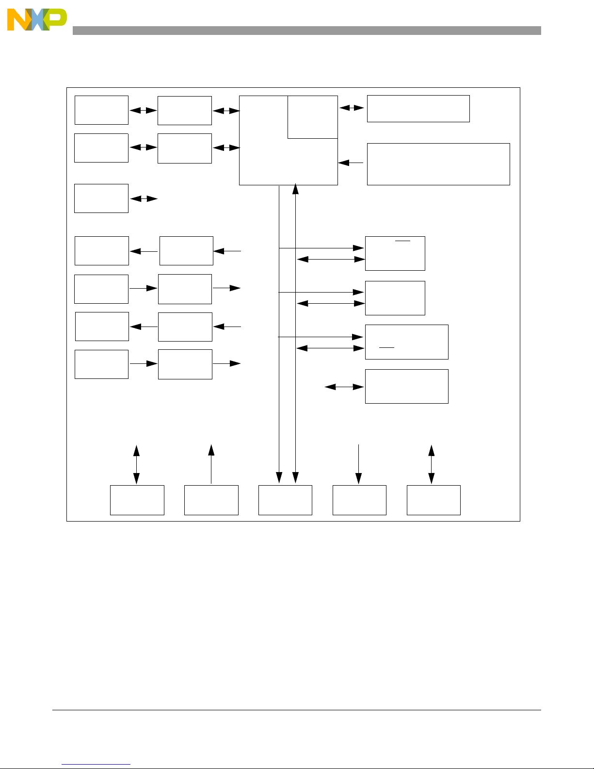
Figure 1-1 shows the M5253EVBE block diagram.
DB-9
Connector
DB-9
Connector
GPIO
Connectors
Headphone
Socket
RCA
Phono plugs
Optical EBU
Transmitter
Optical EBU
Receiver
RS232
Transceiver
CAN
Transceiver
Audio DAC
(I2S2)
Audio ADC
(I2S3)
Audio Out
(EBUOUT1)
Audio In
(EBUIN1)
Addr
[24:1]
Debug
Module
MCF5253
Data
[31:16]
26-pin debug connector
Oscillators: 32.768 KHz
11.2896 MHz
24 MHz
Flash (CS0)
16 bit,3.3v
2MB
SDRAM
16bit 3.3V
8MB
Buffered
IDE I/F
(CS2
/BUFENB2)
Dedicated
ATA I/F
Supports DMA
.
SD Card
Interface
Keypad
1-2 Freescale Semiconductor
(ATD)
TFT Display
Interface
M5253EVBE Users Manual, Rev. 1
B&W Display
I/F (QSPI)
USB
2.0 OTG
Page 9
DB-9
Connector
RS232
Transceiver
Debug
Module
26-pin debug connector
DB-9
Connector
GPIO
Connectors
CAN
Transceiver
Addr
[24:1]
MCF5253
Data
[31:16]
Oscillators: 32.768 KHz
11.2896 MHz
24 MHz
Flash (CS0)
16 bit,3.3v
2MB
SDRAM
16bit 3.3V
8MB
Buffered
IDE I/F
(CS2
/BUFENB2)
Dedicated
ATA I/F
Supports DMA
.
SD Card
Interface
Keypad
(ATD)
TFT Display
Interface
B&W Display
I/F (QSPI)
USB
2.0 OTG
Figure 1-1 M5253EVBE Block Diagram
1.2 System Memory
One on-board Flash ROM (U11) is used in the system. The Am29LV160DB-XX device contains 16 Mbits
of non-volatile storage (1 Mbyte x 16), giving a total of 2 Mbytes of Flash memory. The lower 256 Kbytes
are used to store the M5253EVBE dBUG debugger/monitor firmware that is pre-programmed into the
Flash during factory testing.
The MCF5253 processor has 128 Kbytes of internal SRAM organized as 2 banks of 64 Kbytes. The
SRAM can be used for either data or instruction space.
M5253EVBE Users Manual, Rev. 1
Freescale Semiconductor 1-3
Page 10

There is one SDRAM (U12) device on the PCB. The system ships with 1x4Mbytesx16 of SDRAM
totalling 8 Mbytes of volatile memory.
The internal cache of the MCF5253 is non-blocking. The instruction cache is 8 Kbytes with a 16-byte line
size. The ROM monitor currently does not utilize the cache, but programs downloaded with the ROM
monitor can initialize and use the cache.
1.3 Serial Communication Channels
The MCF5253 processor has 3 built-in UARTs with independent baud rate generators. The signals of all
channels can be passed through the external transceiver to make the channels RS-232 compatible (P4). An
RS-232 serial cable with DB9 connectors is included with the board. UART0 cha nnel is the “TERMINAL”
channel used by dBUG for communication with an external terminal/PC. The “TERMINAL” baud rate
defaults to 115200.
1.4 Parallel I/O Ports
The MCF5253 offers up to 60 lines of general-purpose I/O, of which six are dedicated inputs and three are
dedicated outputs. Seven of the GPIO lines are also available as edge-sensitive interrupt inputs. In
addition, there is one dedicated input for wake-up from low-power mode.
1.5 System Configuration
The M5253EVBE board requires the following items for minimum system configuration:
• The M5253EVBE board (provided)
• Power supply, +7 V to 14 V DC with minimum of 1.0 amp
• RS232C-compatible terminal or a PC with terminal emulation software
• RS232 communication cable (provided)
Refer to Section 2.2.2, “System Initialization” for initial system setup.
1-4 Freescale Semiconductor
M5253EVBE Users Manual, Rev. 1
Page 11
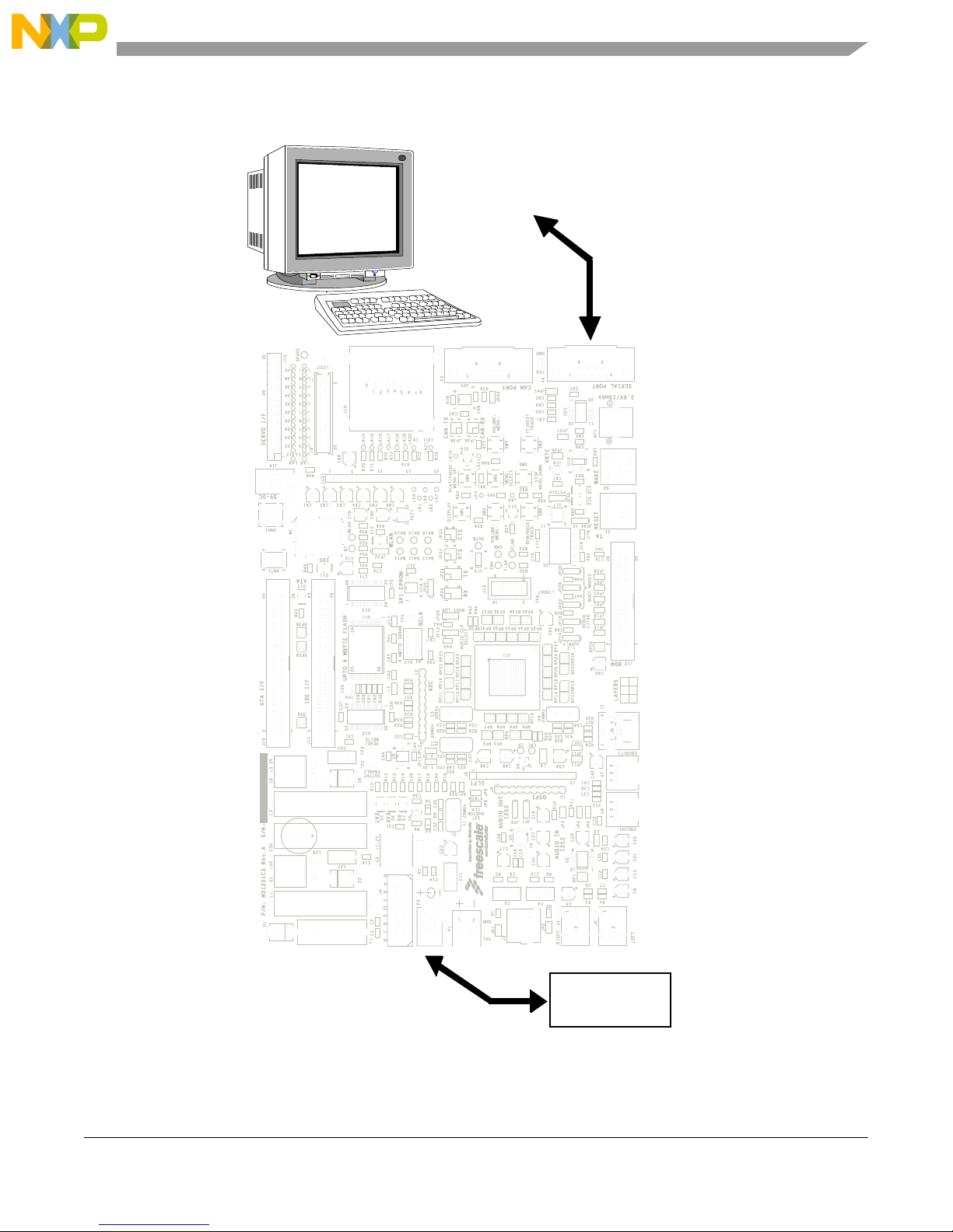
Figure 1-2 displays the minimum system configuration.
dBUG>
RS-232 Terminal or PC
Figure 1-2 Minimum System Configuration
Freescale Semiconductor 1-5
+7.0 to +14 VDC
Input Power
M5253EVBE Users Manual, Rev. 1
Page 12

1.6 Installation and Setup
This section discusses all the steps needed to prepare the board for operation. Read all the sections
carefully before using the board. When you are preparing the board for the first time, be sure to check that
all jumpers are in the default locations.
1.6.1 Unpacking
Unpack the computer board from its shipping box. Save the box for storing or reshipping. Refer to the
following list and verify that all the items are present. You should have received:
• M5253EVBE development system (CE certified)
• Sceptre 9.0 Volt, 2.7 A power supply with WS-047 and WS-048 adapters
• P&E Micro ColdFire USB interface cable
• USB 2.0 cable
• EVB Quickstart Guide (hardcopy)
• Warranty card—920-75133
• Technical Information Center Worldwide Contact List
• Freescale Documentation (http://www.freescale.com/coldfire)
— M5253 Evaluation Board Users Manual (this document)
CAUTION
Avoid touching the MOS devices. Static discharge can and will damage
these devices.
Once you have verified that all the items are present, remove the board from its protective jacket and
anti-static bag. Check the board for any visible damage. Ensure that there are no broken, damaged, or
missing parts. If you have not received all the items listed above or they are damaged, contact Rapid
Design immediately. For contact details, see the front of this manual.
1.6.2 Preparing the Board for Use
The board, as shipped, is ready to be connected to a terminal and power supply without any need for
modification. Figure 1-4 shows the position of the jumpers and connectors.
1.6.3 Providing Power to the Board
The board accepts three means of power supply connection—P1, P2, or J4. Connector P1 is a 2.1 mm
power jack, P2 is a lever-actuated connector, and J4 is a PC disk drive-type power connector. The board
accepts +7 V to +14 V DC at 1.0 amp via either of the connectors. Table 1-2 lists power supply
connections on P2.
1-6 Freescale Semiconductor
M5253EVBE Users Manual, Rev. 1
Page 13

Table 1-1 Power Supply Connections on P2
Contact Number Voltage
1 +7V to +14V DC
2 Ground
1.6.4 Selecting Terminal Baud Rate
The serial channel UAR T0 of the MCF5253 is used for serial communication and has a built in timer . This
timer is used by the dBUG ROM monitor to generate the baud rate used to communicate with a serial
terminal. A number of baud rates can be programmed. On power-up or manual RESET, the dBUG ROM
monitor firmware configures the channel for 115200 baud. Once the dBUG ROM monitor is running, a
SET command may be issued to select any baud rate supported by the ROM monitor. See Section 2.1,
“What Is dBUG?” for the discussion of this command.
1.6.5 Terminal Character Format
The character format of the communication channel is fixed at power-up or RESET. The default character
format is 8 bits per character, no parity and one stop bit with no flow control. It is necessary to ensure that
the terminal or PC is set to this format.
1.6.6 Connecting the Terminal
The board is now ready to be connected to a PC/terminal. Use the RS232 serial cable to connect the
PC/terminal to the M5253EVBE PCB. The cable has a 9-pin female D-sub terminal connector at one end
and a 9-pin male D-sub connector at the other end. Connect the 9-pin male connector to connector P4 on
the M5253EVBE board. Connect the 9-pin female connector to one of the available serial communication
channels normally referred to as COM1 (COM2, etc.) on the PC running terminal emulation software. The
connector on the PC/terminal may be either male 25-pin or 9-pin. It may be necessary to obtain a
25pin-to-9pin adapter to make this connection. If an adapter is required, refer to Figure 1-3, which shows
the pin assignment for the 9-pin connector on the board.
5
Figure 1-3 Pin Assignment for Female (Terminal) Connector
1
69
1.6.7 Using a Personal Computer as a Terminal
A personal computer may be used as a terminal provided a terminal emulation software package is
available. Examples of this software are PROCOMM, KERMIT, QMODEM, Windows 95/98/2000/XP
Hyper Terminal or similar packages. The board should then be connected as described in Section 1.6.6,
“Connecting the Terminal.”
Freescale Semiconductor 1-7
M5253EVBE Users Manual, Rev. 1
Page 14

Once the connection to the PC is made, power may be applied to the PC and the terminal emulation
software can be run. In terminal mode, it is necessary to select the baud rate and character format for the
channel. Most terminal emulation software packages provide a command known as “Alt-p” (press the p
key while pressing the Alt key) to choose the baud rate and character format. The character format should
be 8 bits, no parity, one stop bit. (See Section 1.6.5, “Terminal Character Format.”) The baud rate should
be set to 115200. Power can now be applied to the board.
Pin assignments are as follows:
1. Data Carrier Detect—Output (shorted to pins 4 and 6)
2. Receive Data—Output from board (Receive refers to terminal side.)
3. Transmit Data—Input to board (Transmit refers to terminal side.)
4. Data Terminal Ready—Input (shorted to pin 1 and 6)
5. Signal Ground
6. Data Set Ready—Output (shorted to pins 1 and 4)
7. Request to Send—Input
8. Clear to Send—Output
9. Not connected
1-8 Freescale Semiconductor
M5253EVBE Users Manual, Rev. 1
Page 15
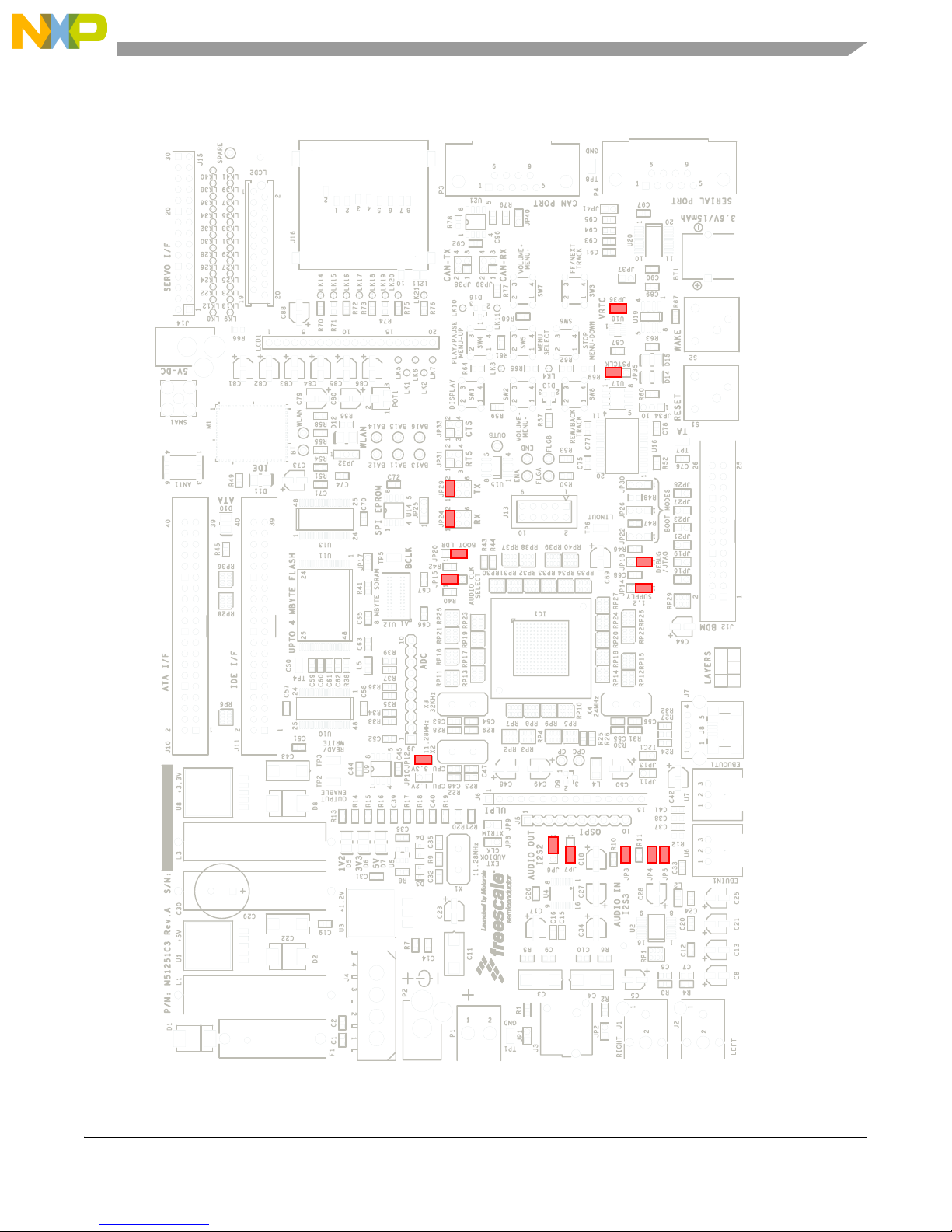
Figure 1-4 shows the default jumper locations for the board.
Freescale Semiconductor 1-9
Figure 1-4 Default Jumper Locations
M5253EVBE Users Manual, Rev. 1
Page 16

1.7 System Power-up and Initial Operation
When all of the cables are connected to the board, power may be applied. The dBUG ROM Monitor
initializes the board and then displays a power-up message on the terminal, which includes the amount of
memory present on the board.
Hard Reset
DRAM Size: 8M
ColdFire MCF5253 on the M5253EVB
Firmware v4c.1b.1a (Built on Feb 1 2007 11:45:04)
Copyright 2006 Freescale Semiconductor, Inc.
Enter 'help' for help.
dBUG>
The board is now ready for operation under the control of the debugger as described in Section 2.2,
“Operational Procedure.” If you do not get the above response, perform the following checks:
1. Make sure that the power supply is properly configured for polarity, voltage level and current
capability (~1A) and is connected to the board.
2. Check that the terminal and board are set for the same character format and baud.
3. Press the RESET button to insure that the board has been initialized properly.
If you still are not receiving the proper response, your board may have been damaged. Contact Rapid PCB
for further instructions. For contact details, see the front of this manual.
1.8 M5253EVBE Jumper Setup
Jumper settings are as follows:
*: Indicates the default setting.
**: Indicates mandatory setting for proper operation.
Table 1-2 Jumper Settings
Jumper Setting Function
JP6 * 1-2 Audio DAC AK4366VT U4 audio format I2S
2-3 Audio DAC AK4366VT U4 audio format 24-bit MSB justified
JP7 1-2 Audio DAC AK4366VT U4 de-emphasis ON
* 2-3 Audio DAC AK4366VT U4 de-emphasis OFF
JP8 Not fitted Enable external audio clock source
JP9 Not fitted Enable XTRIM hardware feature
JP10 Not fitted External 1.2V (core) supply current measurement
JP11,JP13 Not fitted I2S0 5V pull-up (SDA0 and SCL0)
JP12 ** Fitted External 3.3V (pad) supply current measurement
NOTE
1-10 Freescale Semiconductor
M5253EVBE Users Manual, Rev. 1
Page 17

Table 1-2 Jumper Settings (Continued)
Jumper Setting Function
JP14 ** 1-2 1.2V (core) supply from internal regulator
2-3 1.2V (core) supply from external regulator
JP15 * 1-2 Audio clock source taken from CRIN
2-3 Audio clock source taken from external pin (LRCK3)
JP16,JP19 Not fitted I2S1 5V pull-up (SDA1 and SCL1)
JP17 Not fitted SPI EEPROM M25P40 U14 CS enable (QSPICS0)
JP18 ** 1-2 Select BDM debug mode
2-3 Select JTAG debug mode
JP20 1-2 Boot mode select, from internal ROM
* 2-3 Boot mode select, from external memory (CS0)
JP21,JP23,JP27,JP28 Not fitted DDATA signal isolation from BDM interface
JP22,JP26,JP30 Not fitted Internal boot ROM mode select
JP24 * 1-2 (UART0) RS232 transceiver RX select
JP25 1-2 SPI EEPROM M25P40 U14 write protected (WP)
2-3 SPI EEPROM M25P40 U14 write enabled
JP29 * 1-2 (UART0) RS232 transceiver TX select
JP31 Not fitted RS232 transceiver RTS select
JP32 1-2 Wireless module M1 WAIT signal connected to IDEIORDY
2-3 Wireless module M1 WAIT signal connected to TA
JP33 Not fitted RS232 transceiver CTS select
JP34 1-2 Push button S2 connected to interrupt capable GPIO1
2-3 Push button S2 connected to WAKEUP pin
JP36 * Fitted Real Time Clock (RTC) supply isolation / current
measurement
JP37 Not fitted RS232 transceiver INVALID signal connected to GPIO34
JP38 Not fitted CAN transceiver TX select
JP39 Not fitted CAN transceiver RX select
JP40 Not fitted Connect CAN bus termination resistor (120R)
JP41 Not fitted RS232 transceiver READY signal connected to GPIO8
1.9 Using the BDM Port
The MCF5253 microprocessor has a built in debug module referred to as BDM (background debug
module). In order to use the BDM, simply connect the 26-pin debug connector on the board (J12) to the
Freescale Semiconductor 1-11
M5253EVBE Users Manual, Rev. 1
Page 18

P&E BDM wiggler cable provided in the kit. No special setting is needed. Refer to the MCF5253
Reference Manual BDM section for additional instructions.
NOTE
BDM functionality and use are supported via third party developer software
tools.
1-12 Freescale Semiconductor
M5253EVBE Users Manual, Rev. 1
Page 19

Chapter 2
Using the Monitor/Debug Firmware
The M5253EVBE single board computer has a resident firmware package that provides a self-contained
programming and operating environment. The firmware, named dBUG, provides the user with
monitor/debug interface, in-line assembler and disassembly, program download, register and memory
manipulation, and I/O control functions. This chapter is a how-to-use description of the dBUG package,
including the user interface and command structure.
NOTE
The current M5253EVBE dBUG version does not support the network
commands that require an ethernet connection, these commands are
documented to support future firmware releases.
2.1 What Is dBUG?
dBUG is a traditional ROM monitor/debugger that offers a comfortable and intuitive command line
interface that can be used to download and execute code. It contains all the primary features needed in a
debugger to create a useful debugging environment.
dBUG is a resident firmware package for the ColdFire® family single board computers. The firmware
(stored in one 1 Mx16 flash ROM device) provides a self-contained programming and operating
environment. dBUG interacts with the user through pre-defined commands that are entered via the
terminal. These commands are defined in Section 2.4, “Commands.”
The user interface to dBUG is the command line. A number of features have been implemented to achieve
an easy and intuitive command line interface.
dBUG assumes that an 80 x 24 character dumb-terminal is utilized to connect to the debugger. For serial
communications, dBUG requires eight data bits, no parity , and one stop bit, 8N1 with no flow control. The
default baud rate is 115200 but can be changed after the power-up.
The command line prompt is “dBUG>”. Any dBUG command may be entered from this prompt. dBUG
does not allow command lines to exceed 80 characters. Wherever possible, dBUG displays data in 80
columns or less. dBUG echoes each character as it is typed, eliminating the need for any “local echo” on
the terminal side.
In general, dBUG is not case sensitive. Commands may be entered either in upper or lower case, depending
upon the user’s equipment and preference. Only symbol names require that the exact case be used.
Most commands can be recognized by using an abbreviated name. For instance, entering “h” is the same
as entering “help”. Thus, it is not necessary to type the entire command name.
M5253EVBE Users Manual, Rev. 1
Freescale Semiconductor 2-1
Page 20

The commands DI, GO, MD, STEP, and TRACE are used repeatedly when debugging. dBUG recognizes
this and allows for repeated execution of these commands with minimal typing. After a command is
entered, simply press <RETURN> or <ENTER> to invoke the command again. The command is executed
as if no command line parameters were provided.
An additional function called the “TRAP 15 handler” allows the user program to utilize various routines
within dBUG. The TRAP #15 handler is discussed in Section 2.5, “TRAP #15 Functions” on page 2-21.
The operational mode of dBUG is shown in Figure 2-1. After the system initialization, the board waits for
a command-line input from the user terminal. When a proper command is entered, the operation continues
in one of the two basic modes. If the command causes execution of the user program, the dBUG firmware
may or may not be re-entered, at the discretion of the user’s program. For the alternate case, the command
will be executed under control of the dBUG firmware, and after command completion, the system returns
to command entry mode.
During command execution, additional user input may be required depending on the command function.
For commands that accept an optional <width> to modify the memory access size, the valid values are:
• B 8-bit (byte) access
• W 16-bit (word) access
• L 32-bit (long) access
When no <width> option is provided, the default width is .W, 16-bit.
The core ColdFire® register set is maintained by dBUG. These are listed below:
• A0–A7
• D0–D7
•PC
•SR
All control registers on ColdFire® are not readable by the supervisor programming model, and thus not
accessible via dBUG. User code may change these registers, but caution must be exercised as changes may
render dBUG inoperable.
A reference to “SP” (stack pointer) actually refers to general purpose address register seven, “A7.”
2.2 Operational Procedure
System power-up and initial operation are described in detail in Section 1.7, “System Power-up and Initial
Operation.”
2.2.1 System Power-up
1. Be sure the power supply is connected properly prior to power-up.
2. Make sure the terminal is connected to TERMINAL (P4) connector.
3. Turn power on to the board.
Figure 2-1 shows the dBUG operational mode.
2-2 Freescale Semiconductor
M5253EVBE Users Manual, Rev. 1
Page 21

Initialize
No
Execute
Command
Function
No
Command Line
Input from
Te r m in a l ?
Ye s
Does
Command
Line Cause User
Program
Execution?
Ye s
Jump to User
Program and
Begin Execution
Figure 2-1 Flow Diagram of dBUG Operational Mode
2.2.2 System Initialization
The act of powering up the board will initialize the system. The processor is reset and dBUG is invoked.
dBUG performs the following configurations of internal resources during the initialization. The instruction
cache is invalidated and disabled. The Vector Base Register (VBR) points to the Flash. However, a copy
of the exception table is made at address 0x0000_0000 in SDRAM. To take over an exception vector, the
user places the address of the exception handler in the appropriate vector in the vector table located at
0x0000_0000, and then points the VBR to 0x0000_0000.
The Software Watchdog Timer is disabled and internal timers are placed in a stop condition. Interrupt
controller registers initialized with unique interrupt level/priority pairs. Refer to the dBUG source files on
the ColdFire website (http://www.freescale.com/coldfire) for the complete initialization code sequence.
After initialization, the terminal displays the following:
Hard Reset
DRAM Size: 8M
ColdFire MCF5253 on the M5253EVB
Firmware v4c.1b.1a (Built on Feb 1 2007 11:45:04)
Copyright 2006 Freescale Semiconductor, Inc.
Enter 'help' for help.
dBUG>
Freescale Semiconductor 2-3
M5253EVBE Users Manual, Rev. 1
Page 22

If you did not get this response check the setup, refer to Section 1.7, “System Power-up and Initial
Operation.”
Other means can be used to re-initialize the M5253EVBE firmware. These means are discussed in
Section 2.2.2.1, “Hard RESET Button,” Section 2.2.2.2, “ABORT Button,” and Section 2.2.2.3,
“Software Reset Command.”
2.2.2.1 Hard RESET Button
Hard RESET (S1) is the red button. Pressing this button causes all processes to terminate, resets the
MCF5253 processor and board logic, and restarts the dBUG firmware. Pressing the RESET button would
be the appropriate action if all else fails.
2.2.2.2 ABORT Button
ABOR T (S2) is the button located next to the RESET button. The abort function causes an interrupt of the
present processing (a level 7 interrupt on MCF5253) and gives control to the dBUG firmware. This action
differs from RESET in that no processor register or memory contents are changed, the processor and
peripherals are not reset, and dBUG is not restarted. Also, in response to depressing the ABORT button,
the contents of the MCF5253 core internal registers are displayed.
The abort function is most appropriate when software is being debugged. The user can interrupt the
processor without destroying the present state of the system. This is accomplished by forcing a
non-maskable interrupt that will call a dBUG routine that will save the current state of the registers to
shadow registers in the monitor for display to the user. The user will be returned to the ROM monitor
prompt after exception handling.
2.2.2.3 Software Reset Command
dBUG’s command—“RESET”—causes the dBUG to restart as if a hardware reset was invoked.
2.3 Command Line Usage
The user interface to dBUG is the command line. A number of features have been implemented to achieve
an easy and intuitive command line interface.
dBUG assumes that an 80 x 24 ASCII-character dumb terminal is used to connect to the debugger. For
serial communications, dBUG requires eight data bits, no parity, and one stop bit (8N1). The baud rate
default is 115200 bps—a speed commonly available from workstations, personal computers, and
dedicated terminals.
The command line prompt is: dBUG>
Any dBUG command may be entered from this prompt. dBUG does not allow command lines to exceed
80 characters. Wherever possible, dBUG displays data in 80 columns or fewer. dBUG echoes each
character as it is typed, eliminating the need for any local echo on the terminal side.
The <Backspace> and <Delete> keys are recognized as rub-out keys for correcting typographical
mistakes.
2-4 Freescale Semiconductor
M5253EVBE Users Manual, Rev. 1
Page 23

Command lines may be recalled using the <Control>-U, <Control>-D and <Control>-R key sequences.
<Control>-U and <Control>-D cycle up and down through previous command lines. <Control>-R recalls
and executes the last command line.
dBUG is not case-sensitive. Commands may be entered either in uppercase or lowercase, depending upon
the user’s equipment and preference. Only symbol names require that the exact case be used.
Most commands can be recognized by using an abbreviated name. For instance, entering h is the same as
entering help. Thus, it is not necessary to type the entire command name.
The commands DI, GO, MD, STEP, and TRACE are used repeatedly when debugging. dBUG recognizes
this and allows for repeated execution of these commands with minimal typing. After a command is
entered, press the <Return> or <Enter> key to invoke the command again. The command is executed as if
no command line parameters were provided.
2.4 Commands
This section lists the commands that are available with all versions of dBUG. (Some board or CPU
combinations may use additional commands not listed in Table 2-1.)
.
Mnemonic Syntax Description
Table 2-1 dBUG Command Summary
ASM asm <<addr> stmt> Assemble
BC bc addr1 addr2 length Block Compare
BF bf <width> begin end data <inc> Block Fill
BM bm begin end dest Block Move
BR br addr <-r> <-c count> <-t trigger> Breakpoint
BS bs <width> begin end data Block Search
DC dc value Data Convert
DI di<addr> Disassemble
DL dl <offset> Download Serial
DN dn <-c> <-e> <-i> <-s <-o offset>> <filename> Download Network
GO go <addr> Execute
GT gt addr Execute To
HELP help <command> Help
IRD ird <module.register> Internal Register Display
IRM irm module.register data Internal Register Modify
LR lr <width> addr Loop Read
LW lw <width> addr data Loop Write
MD md <width> <begin> <end> Memory Display
MM mm <width> <addr> <data> Memory Modify
Freescale Semiconductor 2-5
M5253EVBE Users Manual, Rev. 1
Page 24

Table 2-1 dBUG Command Summary (Continued)
Mnemonic Syntax Description
MMAP mmap Memory Map Display
RD rd <reg> Register Display
RM rm reg data Register Modify
RESET reset Reset
SD sd Stack Dump
SET set <option value> Set Configurations
SHOW show <option> Show Configurations
STEP step Step (Over)
SYMBOL symbol <symb> <-a symb value> <-r symb> <-C|l|s> Symbol Management
TRACE trace <num> Trace (Into)
UPDBUG updbug Update dBUG
UPUSER upuser <bytes> Update User Flash
VERSION version Show Version
2.4.1 ASM (Assembler)
Usage: ASM <<addr> stmt>
The ASM command is a primitive assembler. The <stmt> is assembled and the resulting code placed at
<addr>. This command has an interactive and non-interactive mode of operation.
The value for address <addr> may be an absolute address specified as a hexadecimal value, or a symbol
name. The value for stmt must be valid assembler mnemonics for the CPU.
For the interactive mode, the user enters the command and the optional <addr>. If the address is not
specified, then the last address is used. The memory contents at the address are disassembled, and the user
prompted for the new assembly. If valid, the new assembly is placed into memory, and the address
incremented accordingly . If the assembly is not valid, then memory is not modified, and an error mes sage
produced. In either case, memory is disassembled and the process repeats.
The user may press the <Enter> or <Return> key to accept the current memory contents and skip to the
next instruction, or a enter period to quit the interactive mode.
In the non-interactive mode, the user specifies the address and the assembly statement on the command
line. The statement is the assembled, and if valid, placed into memory, otherwise an error message is
produced.
Examples:
To place a NOP instruction at address 0x0001_0000, the command is:
asm 10000 nop
2-6 Freescale Semiconductor
M5253EVBE Users Manual, Rev. 1
Page 25

To interactively assembly memory at address 0x0040_0000, the command is:
asm 400000
2.4.2 BC (Block Compare)
Usage: BC addr1 addr2 length
The BC command compares two contiguous blocks of memory on a byte by byte basis. The first block
starts at address addr1 and the second starts at address addr2, both of length bytes.
If the blocks are not identical, the address of the first mismatch is displayed. The value for addresses addr1
and addr2 may be an absolute address specified as a hexadecimal value or a symbol name. The value for
length may be a symbol name or a number converted according to the user defined radix (hexadecimal by
default).
Example:
To verify that the data starting at 0x2_0000 and ending at 0x3_0000 is identical to the data starting at
0x8_0000, the command is:
bc 20000 80000 10000
2.4.3 BF (Block Fill)
Usage: BF <width> begin end data <inc>
The BF command fills a contiguous block of memory starting at address begin, stopping at address end,
with the value data. <Width> modifies the size of the data that is written. If no <width> is specified, the
default of word sized data is used.
The value for addresses begin and end may be an absolute address specified as a hexadecimal value, or a
symbol name. The value for data may be a symbol name, or a number converted according to the
user-defined radix, normally hexadecimal.
The optional value <inc> can be used to increment (or decrement) the data value during the fill.
This command first aligns the starting address for the data access size, and then increments the address
accordingly during the operation. Thus, for the duration of the operation, this command performs
properly-aligned memory accesses.
Examples:
To fill a memory block starting at 0x0002_0000 and ending at 0x0004_0000 with the value 0x1234, the
command is:
bf 20000 40000 1234
T o fill a block of memory starting at 0x0002_0000 and ending at 0x004_0000 with a byte value of 0xAB,
the command is:
bf.b 20000 40000 AB
To zero out the BSS section of the target code (defined by the symbols bss_start and bss_end), the
command is:
Freescale Semiconductor 2-7
M5253EVBE Users Manual, Rev. 1
Page 26

bf bss_start bss_end 0
To fill a block of memory starting at 0x0002_0000 and ending at 0x0004_0000 with data that increments
by 2 for each <width>, the command is:
bf 20000 40000 0 2
2.4.4 BM (Block Move)
Usage: BM begin end dest
The BM command moves a contiguous block of memory starting at address begin and stopping at address
end to the new address dest. The BM command copies memory as a series of bytes, and does not alter the
original block.
The values for addresses begin, end, and dest may be absolute addresses specified as hexadecimal values,
or symbol names. If the destination address overlaps the block defined by begin and end, an error message
is produced and the command exits.
Examples:
To copy a block of memory starting at 0x0004_0000 and ending at 0x0008_0000 to the location
0x0020_0000, the command is:
bm 40000 80000 200000
To copy the target code’s data section (defined by the symbols data_start and data_end) to 0x0020_0000,
the command is:
bm data_start data_end 200000
NOTE
Refer to “upuser” command for copying code/data into Flash memory.
2.4.5 BR (Breakpoints)
Usage: BR addr <-r> <-c count> <-t trigger>
The BR command inserts or removes breakpoints at address addr. The value for addr may be an absolute
address specified as a hexadecimal value, or a symbol name. Count and trigger are numbers converted
according to the user-defined radix, normally hexadecimal.
If no argument is provided to the BR command, a listing of all defined breakpoints is displayed.
The -r option to the BR command removes a breakpoint defined at address addr . If no address is specified
in conjunction with the -r option, then all breakpoints are removed.
Each time a breakpoint is encountered during the execution of target code, its count value is incremented
by one. By default, the initial count value for a breakpoint is zero, but the -c option allows setting the initial
count for the breakpoint.
Each time a breakpoint is encountered during the execution of target code, the count value is compared
against the trigger value. If the count value is equal to or greater than the trigger value, a breakpoint is
2-8 Freescale Semiconductor
M5253EVBE Users Manual, Rev. 1
Page 27

encountered and control returned to dBUG. By default, the initial trigger value for a breakpoint is one, but
the -t option allows setting the initial trigger for the breakpoint.
If no address is specified in conjunction with the -c or -t options, then all breakpoints are initialized to the
values specified by the -c or -t option.
Examples:
To set a breakpoint at the C function main() (symbol _main; see “symbol” command), the command is:
br _main
When the target code is executed and the processor reaches main(), control will be returned to dBUG.
To set a breakpoint at the C function bench() and set its trigger value to 3, the command is:
br _bench -t 3
When the target code is executed, the processor must attempt to execute the function bench() a third time
before returning control back to dBUG.
To remove all breakpoints, the command is:
br -r
2.4.6 BS (Block Search)
Usage: BS <width> begin end data
The BS command searches a contiguous block of memory starting at address begin, stopping at address
end, for the value data. <Width> modifies the size of the data that is compared during the search. If no
<width> is specified, the default of word sized data is used.
The values for addresses begin and end may be absolute addresses specified as hexadecimal values, or
symbol names. The value for data may be a symbol name or a number converted according to the
user-defined radix, normally hexadecimal.
This command first aligns the starting address for the data access size, and then increments the address
accordingly during the operation. Thus, for the duration of the operation, this command performs
properly-aligned memory accesses.
Examples:
To search for the 16-bit value 0x1234 in the memory block starting at 0x0004_0000 and ending at
0x0008_0000:
bs 40000 80000 1234
This reads the 16-bit word located at 0x0004_0000 and compares it against the 16-bit value 0x1234. If no
match is found, then the address is incremented to 0x0004_0002 and the next 16-bit value is read and
compared.
To search for the 32-bit value 0xABCD in the memory block starting at 0x0004_0000 and ending at
0x0008_0000:
bs.l 40000 80000 ABCD
Freescale Semiconductor 2-9
M5253EVBE Users Manual, Rev. 1
Page 28

This reads the 32-bit word located at 0x0004_0000 and compares it against the 32-bit value
0x0000_ABCD. If no match is found, then the address is incremented to 0x0004_0004 and the next 32-bit
value is read and compared.
2.4.7 DC (Data Conversion)
Usage: DC data
The DC command displays the hexadecimal or decimal value data in hexadecimal, binary, and decimal
notation.
The value for data may be a symbol name or an absolute value. If an absolute value passed into the DC
command is prefixed by ‘0x’, then data is interpreted as a hexadecimal value. Otherwise , data is interpreted
as a decimal value.
All values are treated as 32-bit quantities.
Examples:
To display the decimal and binary equivalent of 0x1234, the command is:
dc 0x1234
To display the hexadecimal and binary equivalent of 1234, the command is:
dc 1234
2.4.8 DI (Disassemble)
Usage: DI <addr>
The DI command disassembles target code pointed to by addr. The value for addr may be an absolute
address specified as a hexadecimal value, or a symbol name.
Wherever possible, the disassembler will use information from the symbol table to produce a more
meaningful disassembly. This is especially useful for branch target addresses and subroutine calls.
The DI command attempts to track the address of the last disassembled opcode. If no address is provided
to the DI command, then the DI command uses the address of the last opcode that was disassembled.
The DI command is repeatable.
Examples:
To disassemble code that starts at 0x0004_0000, the command is:
di 40000
To disassemble code of the C function main(), the command is:
di _main
2.4.9 DL (Download Console)
Usage: DL <offset>
2-10 Freescale Semiconductor
M5253EVBE Users Manual, Rev. 1
Page 29

The DL command performs an S-record download of data obtained from the console, typically a serial
port. The value for offset is converted according to the user-defined radix, normally hexadecimal. Please
reference the ColdFire Microprocessor Family Programmer’s Reference Manual for details on the
S-Record format.
If offset is provided, then the destination address of each S-record is adjusted by offset.
The DL command checks the destination download address for validity. If the destination is an address
outside the defined user space, then an error message is displayed and downloading aborted.
If the S-record file contains the entry point address, then the program counter is set to reflect this address.
Examples:
To download an S-record file through the serial port, the command is:
dl
T o download an S-record fi le through the serial port, and add an of fset to the destination address of 0x40,
the command is:
dl 0x40
2.4.10 DN (Download Network)
Usage: DN <-c> <-e> <-i> <-s> <-o offset> <filename>
The DN command downloads code from the network. The DN command handle files which are either
S-record, COFF, ELF or Image formats. The DN command uses Trivial File T ransfer Protocol (TFTP) to
transfer files from a network host.
In general, the type of file to be downloaded and the name of the file must be specified to the DN
command. The -c option indicates a COFF download, the -e option indicates an ELF download, the -i
option indicates an Image download, and the -s indicates an S-record download. The -o option works only
in conjunction with the -s option to indicate an optional offset for S-record download. The filename is
passed directly to the TFTP server and therefore must be a valid filename on the server.
If neither of the -c, -e, -i, -s or filename options are specified, then a default filename and filetype will be
used. Default filename and filetype parameters are manipulated using the SET and SHOW commands.
The DN command checks the destination download address for validity. If the destination is an address
outside the defined user space, then an error message is displayed and downloading aborted.
For ELF and COFF files which contain symbolic debug information, the symbol tables are extracted from
the file during download and used by dBUG. Only global symbols are kept in dBUG. The dBUG symbol
table is not cleared prior to downloading, so it is the user’s responsibility to clear the symbol table as
necessary prior to downloading.
If an entry point address is specified in the S-record, COFF or ELF file, the program counter is set
accordingly.
Examples:
To download an S-record file with the name “srec.out”, the command is:
Freescale Semiconductor 2-11
M5253EVBE Users Manual, Rev. 1
Page 30

dn -s srec.out
To download a COFF file with the name “coff.out”, the command is:
dn -c coff.out
To download a file using the default filetype with the name “bench.out”, the command is:
dn bench.out
To download a file using the default filename and filetype, the command is:
dn
2.4.11 GO (Execute)
Usage: GO <addr>
The GO command executes target code starting at address addr. The value for addr may be an absolute
address specified as a hexadecimal value, or a symbol name.
If no argument is provided, the GO command begins executing instructions at the current program counter .
When the GO command is executed, all user-defined breakpoints are inserted into the target code, and the
context is switched to the target program. Control is only regained when the target code encounters a
breakpoint, illegal instruction, trap #15 exception, or other exception which causes control to be handed
back to dBUG.
The GO command is repeatable.
Examples:
To execute code at the current program counter, the command is:
go
To execute code at the C function main(), the command is:
go _main
To execute code at the address 0x0004_0000, the command is:
go 40000
2.4.12 GT (Execute To)
Usage: GT addr
The GT command inserts a temporary breakpoint at addr and then executes target code starting at the
current program counter . The value for addr may be an absolute address specified as a hexadecimal value,
or a symbol name.
When the GT command is executed, all breakpoints are inserted into the target code, and the context is
switched to the target program. Control is only regained when the target code encounters a breakpoint,
illegal instruction, or other exception which causes control to be handed back to dBUG.
Examples:
2-12 Freescale Semiconductor
M5253EVBE Users Manual, Rev. 1
Page 31

To execute code up to the C function bench(), the command is:
gt _bench
2.4.13 IRD (Internal Register Display)
Usage: IRD <module.register>
This command displays the internal registers of different modules inside the MCF5xxx. In the command
line, module refers to the module name where the register is located and register refers to the specific
register to display.
The registers are organized according to the module to which they belong. The available modules on the
MCF5xxx are CS, DMA0, DMA1, DMA2, DMA3, DRAMC, PP, MBUS, SIM, TIMER1, TIMER2,
UAR T0 and UART1. Refer to the MCF5407 Reference Manual for more information on these modules
and the registers they contain.
Example:
ird sim.rsr
2.4.14 IRM (Internal Register Modify)
Usage: IRM module.register data
This command modifies the contents of the internal registers of different modules inside the MCF5xxx. In
the command line, module refers to the module name where the register is located and register refers to
the specific register to modify. The data parameter specifies the new value to be written into the register.
The registers are organized according to the module to which they belong. The available modules on the
MCF5xxx are CS, DMA0, DMA1, DMA2, DMA3, DRAMC, PP, MBUS, SIM, TIMER1, TIMER2,
UART0, and UART1. Refer to the MCF5407 Reference Manual for more information on these modules
and the registers they contain.
Example:
To modify the TMR register of the first Timer module to the value 0x0021, the command is:
irm timer1.tmr 0021
2.4.15 HELP (Help)
Usage: HELP <command>
The HELP command displays a brief syntax of the commands available within dBUG. In addition, the
address of where user code may start is given. If command is provided, then a brief listing of the syntax of
the specified command is displayed.
Examples:
To obtain a listing of all the commands available within dBUG, the command is:
help
Freescale Semiconductor 2-13
M5253EVBE Users Manual, Rev. 1
Page 32

To obtain help on the breakpoint command, the command is:
help br
2.4.16 LR (Loop Read)
Usage: LR <width> addr
The LR command continually reads the data at addr until a key is pressed. The optional <width> specifies
the size of the data to be read. If no <width> is specified, the command defaults to reading word sized data.
Example:
To continually read the longword data from address 0x2_0000, the command is:
lr.l 20000
2.4.17 LW (Loop Write)
Usage: LW <width> addr data
The LW command continually writes data to addr. The optional width specifies the size of the access to
memory. The default access size is a word.
Examples:
To continually write the longword data 0x1234_5678 to address 0x2_0000, the command is:
lw.l 20000 12345678
Note that the following command writes 0x78 into memory:
lw.b 20000 12345678
2.4.18 MD (Memory Display)
Usage: MD <width> <begin> <end>
The MD command displays a contiguous block of memory starting at address begin and stopping at
address end. The values for addresses begin and end may be absolute addresses specified as hexadecimal
values, or symbol names. Width modifies the size of the data that is displayed. If no <width> is specified,
the default of word sized data is used.
Memory display starts at the address begin. If no beginning address is provided, the MD command uses
the last address that was displayed. If no ending address is provided, then MD will display memory up to
an address that is 128 beyond the starting address.
This command first aligns the starting address for the data access size, and then increments the address
accordingly during the operation. Thus, for the duration of the operation, this command performs
properly-aligned memory accesses.
Examples:
To display memory at address 0x0040_0000, the command is:
md 400000
2-14 Freescale Semiconductor
M5253EVBE Users Manual, Rev. 1
Page 33

T o display memory in the data section (defined by the symbols data_start and data_end), the command is:
md data_start
To display a range of bytes from 0x0004_0000 to 0x0005_0000, the command is:
md.b 40000 50000
To display a range of 32-bit values starting at 0x0004_0000 and ending at 0x0005_0000:
md.l 40000 50000
2.4.19 MM (Memory Modify)
Usage: MM <width> addr <data>
The MM command modifies memory at the address addr. The value for addr may be an absolute address
specified as a hexadecimal value, or a symbol name. Width specifies the size of the data that is modified.
If no <width> is specified, the default of word sized data is used. The value for data may be a symbol name,
or a number converted according to the user-defined radix, normally hexadecimal.
If a value for data is provided, then the MM command immediately sets the contents of addr to data. If no
value for data is provided, then the MM command enters into a loop. The loop obtains a value for data,
sets the contents of the current address to data, increments the address according to the data size, and
repeats. The loop terminates when an invalid entry for the data value is entered; i.e., a period.
This command first aligns the starting address for the data access size, and then increments the address
accordingly during the operation. Thus, for the duration of the operation, this command performs
properly-aligned memory accesses.
Examples:
To set the byte at location 0x0001_0000 to be 0xFF, the command is:
mm.b 10000 FF
To interactively modify memory beginning at 0x0001_0000, the command is:
mm 10000
2.4.20 MMAP (Memory Map Display)
Usage: mmap
This command displays the memory map information for the M5253EVBE evaluation board. The
information displayed includes the type of memory , the start and end a ddress of the memory, and the port
size of the memory. The display also includes information on how the chip-selects are used on the board.
Here is an example of the output from this command:
Type Start End Port Size
--------------------------------------------------SDRAM 0x00000000 0x003FFFFF 32-bit
Vector Table 0x00000000 0x000003FF 32-bit
USER SPACE 0x00020000 0x003FFFFF 32-bit
MBAR 0x10000000 0x100003FF 32-bit
Freescale Semiconductor 2-15
M5253EVBE Users Manual, Rev. 1
Page 34

Internal SRAM 0x20000000 0x20000FFF 32-bit
External SRAM 0x30000000 0x3007FFFF 32-bit
Flash 0xFFE00000 0xFFFFFFFF 16-bit
Chip Selects
---------------CS0 Flash
CS1 Ethernet controller
CS2 not in use
CS3 not in use
2.4.21 RD (Register Display)
Usage: RD <reg>
The RD command displays the register set of the target. If no argument for reg is provided, then all
registers are displayed. Otherwise, the value for reg is displayed.
dBUG preserves the registers by storing a copy of the register set in a buffer. The RD command displays
register values from the register buffer.
Examples:
To display all the registers and their values, the command is:
rd
To display only the program counter:
rd pc
Here is an example of the output from this command:
PC: 00000000 SR: 2000 [t.Sm.000...xnzvc]
An: 00000000 00000000 00000000 00000000 00000000 00000000 00000000 01000000
Dn: 00000000 00000000 00000000 00000000 00000000 00000000 00000000 00000000
2.4.22 RM (Register Modify)
Usage: RM reg data
The RM command modifies the contents of the register reg to data. The value for reg is the name of the
register, and the value for data may be a symbol name, or it is converted according to the user-defined
radix, normally hexadecimal.
dBUG preserves the registers by storing a copy of the register set in a buffer. The RM command updates
the copy of the register in the buffer . The actual value will not be written to the register until target code is
executed.
Examples:
To change register D0 on MC68000 and ColdFire to contain the value 0x1234, the command is:
rm D0 1234
2-16 Freescale Semiconductor
M5253EVBE Users Manual, Rev. 1
Page 35

2.4.23 RESET (Reset the Board and dBUG)
Usage: RESET
The RESET command resets the board and dBUG to their initial power-on states.
The RESET command executes the same sequence of code that occurs at power-on. If the RESET
command fails to reset the board adequately, cycle the power or press the reset button.
Examples:
To reset the board and clear the dBUG data structures, the command is:
reset
2.4.24 SET (Set Configurations)
Usage: SET <option value>
The SET command allows the setting of user-configurable options within dBUG. With no arguments, SET
displays the options and values available. The SHOW command displays the settings in the appropriate
format. The standard set of options is listed below.
• baud—This is the baud rate for the first serial port on the board. All communications between
dBUG and the user occur using either 9600 or 19200 bps, eight data bits, no parity, and one stop
bit, 8N1, with no flow control.
• base—This is the default radix for use in converting a number from its ASCII text representation
to the internal quantity used by dBUG. The default is hexadecimal (base 16), and other choices are
binary (base 2), octal (base 8), and decimal (base 10).
• client—This is the network Internet Protocol (IP) address of the board. For network
communications, the client IP is required to be set to a unique value, usually assigned by your local
network administrator.
• server—This is the network IP address of the machine which contains files accessible via TFTP.
Your local network administrator will have this information and can assist in properly configuring
a TFTP server if one does not exist.
• gateway—This is the network IP address of the gateway for your local subnetwork. If the client IP
address and server IP address are not on the same subnetwork, then this option must be properly
set. Your local network administrator will have this information.
• netmask—This is the network address mask to determine if use of a gateway is required. This field
must be properly set. Your local network administrator will have this information.
• filename—This is the default filename to be used for network download if no name is provided to
the DN command.
• filetype—This is the default file type to be used for network download if no type is provided to the
DN command. Valid values are: “srecord”, “coff”, and “elf”.
• mac—This is the ethernet Media Access Control (MAC) address (a.k.a hardware address) for the
evaluation board. This should be set to a unique value, and the most significant nibble should
always be even.
Freescale Semiconductor 2-17
M5253EVBE Users Manual, Rev. 1
Page 36

Examples:
To set the baud rate of the board to be 19200, the command is:
set baud 19200
NOTE
See the SHOW command for a display containing the correct formatting of
these options.
2.4.25 SHOW (Show Configurations)
Usage: SHOW <option>
The SHOW command displays the settings of the user-configurable options within dBUG. When no option
is provided, SHOW displays all options and values.
Examples:
To display all options and settings, the command is:
show
To display the current baud rate of the board, the command is:
show baud
Here is an example of the output from a show command:
dBUG> show
base: 16
baud: 19200
server: 192.0.0.1
client: 192.0.0.2
gateway: 0.0.0.0
netmask: 255.255.255.0
filename: test.srec
filetype: S-Record
mac: 00:CF:52:49:C3:01
2.4.26 STEP (Step Over)
Usage: STEP
The STEP command can be used to “step over” a subroutine call, rather than tracing every instruction in
the subroutine. The ST command sets a temporary breakpoint one instruction beyond the current program
counter and then executes the target code.
The STEP command can be used to “step over” BSR and JSR instructions.
The STEP command will work for other instructions as well, but note that if the STEP command is used
with an instruction that will not return, i.e. BRA, then the temporary breakpoint may never be encountered
and dBUG may never regain control.
2-18 Freescale Semiconductor
M5253EVBE Users Manual, Rev. 1
Page 37

Examples:
To pass over a subroutine call, the command is:
step
2.4.27 SYMBOL (Symbol Name Management)
Usage: SYMBOL <symb> <-a symb value> <-r symb> <-c|l|s>
The SYMBOL command adds or removes symbol names from the symbol table. If only a symbol name is
provided to the SYMBOL command, then the symbol table is searched for a match on the symbol name
and its information displayed.
The -a option adds a symbol name and its value into the symbol table. The -r option removes a symbol
name from the table.
The -c option clears the entire symbol table, the -l option lists the contents of the symbol table, and the -s
option displays usage information for the symbol table.
Symbol names contained in the symbol table are truncated to 31 characters. Any symbol table lookups,
either by the SYMBOL command or by the disassembler, will only use the first 31 characters. Symbol
names are case-sensitive.
Symbols can also be added to the symbol table via in-line assembly labels and ethernet downloads of ELF
formatted files.
Examples:
To define the symbol “main” to have the value 0x0004_0000, the command is:
symbol -a main 40000
To remove the symbol “junk” from the table, the command is:
symbol -r junk
To see how full the symbol table is, the command is:
symbol -s
To display the symbol table, the command is:
symbol -l
2.4.28 TRACE (Trace Into)
Usage: TRACE <num>
The TRACE command allows single-instruction execution. If num is provided, then num instructions are
executed before control is handed back to dBUG. The value for num is a decimal number.
The TRACE command sets bits in the processors’ supervisor registers to achieve single-instruction
execution, and the target code executed. Control returns to dBUG after a single-instruction execution of
the target code.
This command is repeatable.
Freescale Semiconductor 2-19
M5253EVBE Users Manual, Rev. 1
Page 38

Examples:
To trace one instruction at the program counter, the command is:
tr
To trace 20 instructions from the program counter, the command is:
tr 20
2.4.29 UPDBUG (Update dBUG)
Usage: UPDBUG
The UPDBUG command is used to update the dBUG image in Flash. When updates to the M5253EVBE
dBUG are available, the updated image is downloaded to address 0x0002_0000. The new image is placed
into Flash using the UPDBUG command. The user is prompted for verification before performing the
operation. Use this command with extreme caution, as any error can render dBUG useless!
2.4.30 UPUSER (Update User Flash)
Usage: UPUSER <bytes>
The UPUSER command places user code and data into space allocated for the user in Flash. The optional
parameter bytes specifies the number of bytes to copy into the user portion of Flash.If the bytes parameter
is omitted, then this command writes to the entire user space. There are seven sectors of 256K each
available as user space. Users access this memory starting at address 0xFFE4_0000.
Examples:
To program all 7 sectors of user Flash, the command is:
upuser
To program only 1000 bytes into user Flash, the command is:
upuser 1000
2.4.31 VERSION (Display dBUG Version)
Usage: VERSION
The VERSION command displays the version information for dBUG. The dBUG version, build number
and build date are all given.
The version number is separated by a decimal, for example, “v 2b.1c.1a”.
In this example, v 2b . 1c . 1a
dBUG common
major and minor
revision
CPU major
and minor
revision
The version date is the day and time at which the entire dBUG monitor was compiled and built.
{
{
{
board major
and minor
revision
2-20 Freescale Semiconductor
M5253EVBE Users Manual, Rev. 1
Page 39

Examples:
To display the version of the dBUG monitor, the command is:
version
2.5 TRAP #15 Functions
An additional utility within the dBUG firmware is a function called the TRAP 15 handler. This function
can be called by the user program to utilize various routines within the dBUG, to perform a special task,
and to return control to the dBUG. This section describes the TRAP 15 handler and how it is used.
There are four TRAP #15 functions. These are: OUT_CHAR, IN_CHAR, CHAR_PRESENT, and
EXIT_TO_dBUG.
2.5.1 OUT_CHAR
This function (function code 0x0013) sends a character, which is in lower 8 bits of D1, to the terminal.
Assembly example:
/* assume d1 contains the character */
move.l #$0013,d0 Selects the function
TRAP #15 The character in d1 is sent to terminal
C example:
void board_out_char (int ch)
{
/* If your C compiler produces a LINK/UNLK pair for this routine,
* then use the following code which takes this into account
*/
#if l
/* LINK a6,#0 -- produced by C compiler */
asm (“ move.l8(a6),d1”); /* put ‘ch’into d1 */
asm (“ move.l#0x0013,d0”); /* select the function */
asm (“ trap#15”); /* make the call */
/* UNLK a6 -- produced by C compiler */
#else
/* If C compiler does not produce a LINK/UNLK pair, the use
* the following code.
*/
asm (“ move.l4(sp),d1”); /* put ‘ch’into d1 */
asm (“ move.l#0x0013,d0”); /* select the function */
asm (“ trap#15”); /* make the call */
#endif
}
2.5.2 IN_CHAR
This function (function code 0x0010) returns an input character (from the terminal) to the caller. The
returned character is in D1.
Assembly example:
move.l #$0010,d0 Select the function
Freescale Semiconductor 2-21
M5253EVBE Users Manual, Rev. 1
Page 40

trap #15 Make the call, the input character is in d1.
C example:
int board_in_char (void)
{
asm (“ move.l#0x0010,d0”); /* select the function */
asm (“ trap#15”); /* make the call */
asm (“ move.ld1,d0”); /* put the character in d0 */
}
2.5.3 CHAR_PRESENT
This function (function code 0x0014) checks if an input character is present to receive. A value of zero is
returned in D0 when no character is present. A non-zero value in D0 means a character is present.
Assembly example:
move.l #$0014,d0 Select the function
trap #15 Make the call, d0 contains the response (yes/no).
C example:
int board_char_present (void)
{
asm (“ move.l#0x0014,d0”); /* select the function */
asm (“ trap#15”); /* make the call */
}
2.5.4 EXIT_TO_dBUG
This function (function code 0x0000) transfers the control back to the dBUG by terminating the user code.
The register context is preserved.
Assembly example:
move.l #$0000,d0 Select the function
trap #15 Make the call, exit to dBUG.
C example:
void board_exit_to_dbug (void)
{
asm (“ move.l#0x0000,d0”); /* select the function */
asm (“ trap#15”); /* exit and transfer to dBUG */
}
2-22 Freescale Semiconductor
M5253EVBE Users Manual, Rev. 1
Page 41

Chapter 3
Hardware Description and Reconfiguration
This chapter provides a functional description of the M5253EVBE board hardware. With the description
given here and the schematic diagrams in Appendix A, “Schematics,” the user can gain a good
understanding of the board's design. In this manual, an active low signal is indicated by a bar over the
signal name.
3.1 Processor and Support Logic
This part of the chapter discusses the CPU and general support logic on the M5253EVBE board. See the
MCF5253 Reference Manual for more detailed information.
3.1.1 Processor
The microprocessor used on the M5253EVBE is the highly integrated ColdFire® MCF5253, 32-bit
processor. The MCF5253 implements a Version 2 ColdFire core with 8-Kbyte instruction cache, three
UAR T channels, two timers, 128-Kbytes of SRAM, a QSPI (Queued Serial Peripheral Interface) module,
two I2C modules, three I2S modules, an IDE module, a dedicate ATA interface with DMA support, two
FlexCAN modules, an OTG USB 2.0 controller with integrated physical interface, real time clock (R TC),
a Flash memory stick interface, 60 parallel I/O ports (which are multiplexed with other signals) and the
system integration module (SIM). All of the core processor registers are 32 bits wide except for the status
register (SR) which is 16 bits wide. This processor communicates with external devices over a 16-bit wide
data bus, D[31:16]. The chip can address 64 Mbytes of memory space using a 25-bit wide address bus and
internal chip-select logic.
The MCF5253 processor has the capability to support both an IEEE JTAG-compatible port and a BDM
debug port. These ports are multiplexed and can be used with third party tools to allow the user to
download code to the board. The board is configured to boot up in the normal/BDM mode of operation.
The BDM signals are available at port (J12). The processor also has the logic to generate up to four (4)
chip selects, and support for a bank of SDRAM (included on the evaluation board as 8 Mbytes in total
configured as 4 M x 16). The SDRAM_CS1
SDRAM.
signal is used to provide selection and control of this bank of
3.1.2 Reset Logic
The reset logic provides system initialization. Reset occurs during power-on or via assertion of the signal
RESET
the entire processor/system.
A hard reset and voltage sense controller (U18) is used to produce an active low power-on RESET signal.
The reset switch S1 is fed into U18 which generates the signal which is fed to the MCF5253 reset, RESET
Freescale Semiconductor 3-1
which causes the MCF5253 to reset. Reset is also triggered by the reset switch (S1) which resets
M5253EVBE Users Manual, Rev. 1
.
Page 42

The RESET signal is an open collector signal and so can be wire OR’ed with other reset signals from
additional peripherals.
dBUG configures the MCF5253 microprocessor internal resources during initialization. The instruction
cache is invalidated and disabled. The vector base register, VBR, contains an address which initially points
to the flash memory. The contents of the exception table are written to address 0x0000_0000 in the
SDRAM. The software watchdog timer is disabled, the bus monitor is enabled, and the internal timers are
placed in a stop condition. The interrupt controller registers are initialized with unique interrupt
level/priority pairs. A memory map for the entire board can be seen in Table 3-1.
3.1.3 HIZ Signal
The assertion of the HIZ signal forces all output drivers to a high-impedance state. On the M5253EVBE
board the high impedance signal is pulled to +3.3V via a 4.7K pull-up resistor, ensuring that the output
drivers will not be in a high-impedance state during reset.
3.1.4 Clock Circuitry
The M5253EVBE board uses a 11.2896 MHz crystal (X2 on the schematics) to provide the clock to the
processor (IC1). In addition to the 11.2896 MHz crystal, there is also a 24 MHz crystal (X4) which feeds
the USB section of IC1, a 32.768 kHz crystal (X3) which feeds the RTC section of IC1 and a second
11.2896 MHz crystal (X1) that can be used to provide an external audio clock source
3.1.5 Watchdog Timer
The duration of the watchdog is selected by the SWT[1:0] bits in the system protection and control register
(SYPCR), SWT[1:0] = 11 gives a maximum timeout period of 228/system frequency . The dBUG monitor
initializes these bits with the value 0x11, which provides the maximum time-out period, but dBUG does
NOT enable the watchdog timer via the SYPCR[SWE] bit.
3.1.6 Interrupt Sources
The ColdFire family of processors can receive seven levels of interrupt priorities. When the processor
receives an interrupt which has a higher priority than the current interrupt mask (in the status register), it
will perform an interrupt acknowledge cycle at the end of the current instruction cycle. This interrupt
acknowledge cycle indicates to the source of the interrupt that the request is being acknowledged and the
device should provide the proper vector number to indicate where the service routine for this interrupt level
is located. If the source of interrupt is not capable of providing a vector, its interrupt should be set up as an
autovector interrupt which directs the processor to a predefined entry in the exception table. (See the
MCF5253 Reference Manual).
The processor goes to an exception routine via the exception table. This table is stored in the Flash
EEPROM. The address of the table location is stored in the VBR. The dBUG ROM monitor writes a copy
of the exception table into the RAM starting at 0x0000_0000. To set an exception vector, the user places
the address of the exception handler in the appropriate vector in the vector table located at 0x0000_0000
and then points the VBR to 0x0000_0000.
3-2 Freescale Semiconductor
M5253EVBE Users Manual, Rev. 1
Page 43

The MCF5253 microprocessor has seven external interrupt request lines INT[6:0], all of which are
multiplexed with other functions. The interrupt controller is capable of providing up to 75 interrupt
sources. These sources include:
• External interrupt signals INT[6:0]
• Software watchdog timer module
• Two general purpose timer modules
• UART module
•I2C module
• Audio interface modules
• DMA module
• QSPI module
• CAN module
• USB module
• ATA module
• Flash media module
All external interrupt inputs are edge sensitive. The active level is programmable. An interrupt request
must be held valid until an IACK cycle starts to guarantee correct processing. Each interrupt input can have
its priority programmed by setting the xIPL[2:0] bits in the Interrupt Control Registers.
NOTE
No interrupt sources should have the same level and priority as another.
Programming two interrupt sources with the same level and priority can
result in undefined operation.
The M5253EVBE hardware uses INT1 to support the ABORT function using the ABORT switch (S2).
This switch is used to force an interrupt (level 7, priority 3) if the user's program execution should be
aborted without issuing a RESET command. See Section 2.2.2.2, “ABORT Button,” for more information
on ABORT.) Since the ABORT switch is not capable of generating a vector in response to a level seven
interrupt acknowledge from the processor, the dBUG programs this interrupt request for autovector mode.
3.1.7 Internal SRAM
The MCF5253 processor has 128 Kbtyes of internal memory which may be programmed as data or
instruction memory . This memory is mapped to 0x2000_0000 and configured as data space but is not used
by the dBUG monitor except during system initialization. After system initialization is complete, the
internal memory is available to the user. The memory can be relocated to any 32-Kbyte boundary.
3.1.8 MCF5253 Registers and Memory Map
The memory and I/O resources of the M5253EVBE hardware are divided into two groups, MCF5253
internal and external resources. All the I/O registers are memory mapped.
Freescale Semiconductor 3-3
M5253EVBE Users Manual, Rev. 1
Page 44

The MCF5253 processor has built in logic and up to four chip-select pins (CS[3:0]) which are used to
enable external memory and I/O devices. In addition there are SDRAS and SDCAS lines available for
controlling SDRAMs. There are registers to specify the address range, type of access and the method of
TA generation for each chip-select. These registers are programmed by the dBUG monitor to map the
external memory and I/O devices.
The M5253EVBE uses the following signals to select external peripherals:
•CS0 to enable the Flash ROM (See Section 3.1.13, “Flash ROM.”)
• SDRAS, SDCAS, and SDRAM_CS1 to enable the SDRAM (See Section 3.1.12, “SDRAM.”)
The chip select mechanism of the MCF5253 processor allows the memory mapping to be defined for the
required memory space (user/supervisor, program/data spaces).
All of the MCF5253 internal registers, configuration registers, parallel I/O port registers, UAR T registers
and system control registers are mapped by the MBAR registers at any 1- KByte boundary . The MBAR1
register is mapped to 0x1000_0000 and MBAR2 mapped to 0x8000_0000 by the dBUG monitor. For a
complete map of these registers, see the MCF5253 Reference Manual.
The M5253EVBE board has 8 Mbytes of SDRAM installed. See Section 3.1.12, “SDRAM” for a
discussion of the SDRAM on the board. The dBUG ROM monitor is programmed in one AMD
AM29L V160DB-90 flash ROM, which occupies 2 Mbytes of the address space. The first 256 Kbytes (i.e.,
the first sector) are used by the ROM monitor and the remainder is left for the user. (See Section 3.1.13,
“Flash ROM.”)
Figure 3-1 shows the M5253EVBE memory map.
Table 3-1 The M5253EVBE Memory Map
Address Range Signal and Device Memory Access Time
0x0000_0000–0x0002_0000 SDRAM space for dBug ROM monitor use Refer to manufacturer specification
0x0002_0000–0x003F_FFFF SDRAM space Refer to manufacturer specification
0x1000_0000–0x1000_03FF System Integration Module (SIM) registers Internal access
0x1000_0000–0x1000_0054 MBAR—Module base address register Refer to MCF5253RM SIM section
0x8000_0000–0x8000_0198 MBAR2—Module base address register 2 Refer to MCF5253RM SIM section
0x2000_0000–0x2000_0FFF SRAM1 Internal access (1 cycle)
0x2001_0000–0x2000_17FF SRAM0 Internal access (1 cycle)
0xFFE0_0000–0xFFFF_FFFF CS0
, 2M Flash ROM 8-7-7-7
All of the unused area of the memory map is available to the user.
3.1.9 Reset Vector Mapping
After reset, the processor attempts to read the initial stack pointer and program counter values from
locations 0x0000_0000 & 0x0000_0004 (the first eight bytes of memory space). This requires the board
to have a non-volatile memory device in this range with the correct information stored in it. In some
systems, however, it is preferred to have RAM starting at address 0x0000_0000. The MCF5253 processor
3-4 Freescale Semiconductor
M5253EVBE Users Manual, Rev. 1
Page 45

chip-select zero (CS0) responds to any accesses after reset until the CSMR0 is written. Since CS0 (the
global chip select) is connected to the Flash ROM (U11), the Flash ROM initially appears at address
0x0000_0000 which provides the initial stack pointer and program counter (the first eight bytes of the
Flash ROM). The initialization routine then programs the chip-select logic, locates the Flash ROM to start
at 0xFFE0_0000, and configures the rest of the internal and external peripherals.
3.1.10 TA Generation
The processor starts a bus cycle by asserting CSx with the other control signals. The processor then waits
for a transfer acknowledgment (TA) either from within (auto acknowledge—AA mode) or from the
externally addressed device before it can complete the bus cycle. TA is used to indicate the completion of
the bus cycle. It also allows devices with different access times to communicate with the processor
properly (that is, asynchronously). The MCF5253 processor, as part of the chip-select logic, has a built-in
mechanism to generate T A for all external devices which do not have the capability to generate this signal.
For example the Flash ROM cannot generate a TA signal. The chip-select logic is programmed by the
dBUG ROM monitor to generate TA internally after a pre-programmed number of wait states.
3.1.11 Wait State Generator
The Flash ROM and SDRAM on the board may require some adjustments to the cycle time of the
processor to make them compatible with the processor’ s external bus speed. T o extend the CPU bus cycles
for the slower devices, the chip-select logic of the MCF5253 processor can be programmed to generate an
internal TA after a given number of wait states. See Table 3-1 for information about the address space of
the memory and refer to the manufacturer’s specification for wait state requirements of the SDRAM and
Flash ROM.
3.1.12 SDRAM
The M5253EVBE has one 64-Mbit device on the board, in a 16-bit wide data bus configuration. The
MCF5253 processor supports one bank of SDRAM, which on this board is represented by SDRAM
device, (U12). These are connected to the MCF5253 to provide 4Mx16 of memory.
3.1.13 Flash ROM
There is one 2-Mbyte Flash ROM on the M5253EVBE, (U11).
The board is shipped with one AMD AM29LV160DB, 2-Mbyte Flash ROM. The first 256 Kbytes of the
Flash contains the ROM Monitor firmware dBUG. The remaining Flash memory is available to the user.
The MCF5253 chip-select logic can be programmed to generate the TA
for CS0 signal after a certain
number of wait states (that is, auto-acknowledge mode). The dBUG monitor programs this parameter to
be six wait-states.
3.2 Serial Communication Channels
The M5253EVBE offers five types of serial communications channels. They are discussed in this section.
M5253EVBE Users Manual, Rev. 1
Freescale Semiconductor 3-5
Page 46

3.2.1 UARTs
The MCF5253 device has three built-in UARTs, each with its own software programmable baud rate
generator. UART0 is the ROM Monitor to Terminal output. The ROM Monitor programs the interrupt
level for UART0 to Level 3, priority 2 and autovector mode of operation.
3.2.2 QSPI Module
The QSPI (Queued Serial Peripheral Interface) module provides a serial peripheral interface with queued
transfer capability. It will support up to 16 stacked transfers at one time, minimizing CPU intervention
between transfers. Transfer RAMs in the QSPI are indirectly accessible using address and data registers.
Functionality is very similar, but not identical, to the QSPI portion of the QSM (Queued Serial Module)
implemented in the MC68332 processor.
• Programmable queue to support up to 16 transfers without user intervention
• Supports transfer sizes of 8 to 16 bits in 1-bit increments
• Four peripheral chip-select lines for control of up to 15 devices
• Baud rates from 274.5 Kbps to 17.5 Mbps at 140 MHz.
• Programmable delays before and after transfers
• Programmable clock phase and polarity
• Supports wrap-around mode for continuous transfers
The QSPI signals from the MCF5253 device are brought out to connector (J5). Some of these signals are
multiplexed with other functions.
3.2.3 I2C Modules
The MCF5253 processor’s two I2C modules include the following features:
• Compatibility with the I2C bus standard
• Multimaster operation
• Software programmable for one of 64 different clock frequencies
• Software selectable acknowledge bit
• Interrupt driven byte by byte data transfer
• Arbitration-lost interrupt with auto mode switching from master to slave
• Calling address identification interrupt
• Start and stop signal generation and detection
• Repeated start signal generation
• Acknowledge bit generation and detection
• Bus busy detection
3.2.4 FlexCAN Modules
The MCF5253 processor’s two FlexCAN modules includes the following features:
3-6 Freescale Semiconductor
M5253EVBE Users Manual, Rev. 1
Page 47

• Full implementation of the CAN protocol specification version 2.0B
— Standard data and remote frames (up to 109 bits long)
— Extended data and remote frames (up to 127 bits long)
— 0–8 bytes data length
— Programmable bit rate up to 1 Mbps
— Content-related addressing
• Up to 32 flexible message buffers of zero to eight bytes data length, each configurable as Rx or Tx,
all supporting standard and extended messages
• Listen-only mode capability
• Three programmable mask registers: global (for MBs 0–13 and 16–31), special for MB14, and
special for MB15
• Programmable transmission priority scheme: lowest ID or lowest buffer number
• Time stamp based on 16-bit, free-running timer
• Global network time, synchronized by a specific message
• Programmable I/O modes
• Maskable interrupts
• Independent of the transmission medium (an external transceiver assumed)
• Open-network architecture
• Multimaster bus
• High immunity to EMI
• Short latency time due to an arbitration scheme for high-priority messages
3.2.5 USB 2.0 OTG Module
The MCF5253 processor’s USB 2.0 OTG module includes the following features:
• Compliance with USB specification revision 2.0
• Support for operation as a standalone USB host controller, including support of enhanced host
controller interface (EHCI)
• USB device mode
• USB On-The-Go mode, including host capability
• Support for high-speed (480 Mbps), full-speed (12 Mbps), and low-speed host (1.5 Mbit/s)
operations
• Support for internal PHY (with UTMI+ interface) and external PHYs with ULPI interface
• Support for operation as a standalone USB device
• Support for one upstream facing port
— Support for four programmable, bidirectional USB endpoints
— Host mode support for direct connect of FS/LS devices.
Freescale Semiconductor 3-7
M5253EVBE Users Manual, Rev. 1
Page 48

3.3 General Purpose I/O Pins
The MCF5253 offers 60-bits of general-purpose I/O of which 6 are dedicated general purpose inputs and
3 are dedicated general purpose outputs. Seven of the GPIO lines are also available as edge sensitive
interrupt inputs plus one dedicated pin is used to generate a WAKEUP interrupt from low power mode.
The functions of all I/O pins are individually programmable, since they are multiplexed with other pin
functions. All general-purpose I/O pins (unless dedicated as either only input or output) can be individually
selected as input or output pins. After reset, all software configurable multi-function GPIO pins default to
general purpose input pins. At the same time, all multifunction pins that are not shared with a GPIO pin
default to high impedance. Internal pullup resistors avoid unknown read values in order to reduce power
consumption. They remain active until the corresponding port direction registers are programmed.
Control registers are provided for each pin to select the function (GPIO or peripheral pin) assigned to each
pin individually. Pins can have from 1 to 4 functions including GPIO.
3.4 Audio Module
The MCF5253 processor’s audio module includes the following features:
• Support for reception and transmission of digital audio over serial interfaces IIS/EIAJ and digital
interface IEC958
• 3x IIS/EIAJ interfaces
• 2x IEC958 receivers (4x multiplexed inputs)
• 1x IEC958 transmitter - two outputs - one with professional subcoding, one with consumer
subcoding
• Allows direct transmission of received audio to an audio transmitter without CPU intervention.
• IEC958 receivers and transmitter support main audio, plus handling of IEC958 C, U and V
sub-channels
• Frequency measurement block - precise measurement of the incoming sample frequency
3.5 Analog to Digital Converter (ADC) Module
The MCF5253 processor’s ADC module includes the following features:
• Sigma-Delta based ADC with 12-bit resolution
• Six dedicated inputs—ADIN0/GPI52, ADIN1/GPI53, ADIN2/GPI54, ADIN3/GPI55,
ADIN4/GPI56, and ADIN5/GPI57
• Single output—ADOUT/SCLK4/GPIO58, provides the reference voltage which requires an
external integrator (resistor/capacitor circuit)
• Software interrupt provided when the ADC measurement is complete
3.6 Flash Memory Card/IDE Interface Module
The MCF5253 memory bus allows connection of an IDE hard disk drive or SmartMedia flash card with a
minimum of external hardware. It can interface with both an IDE device and a SmartMedia device
3-8 Freescale Semiconductor
M5253EVBE Users Manual, Rev. 1
Page 49

connected, although both cannot be supported simultaneously, as the IDE-DIOR and IDE-DIOW signals
can only be used to interface to one or the other.
3.7 ATA Interface Module
The MCF5253 processor’s ATA interface module includes the following features:
• Programmable timing on the ATA bus. The interface works with wide range of bus frequencies.
• Compliance with ATA-6 specification
— Support for PIO modes 0, 1, 2, 3, and 4
— Support for multiword DMA modes 0, 1, and 2
— Support for ultra DMA modes 0, 1, 2, 3, and 4 with bus clock of at least 50 MHz
— Support for ultra DMA mode 5 with bus clock of at least 80 MHz
• 128-byte FIFO part of interface
• FIFO receive alarm and FIFO transmit alarm to DMA unit
• Zero-wait cycles transfer between DMA bus and FIFO, which allows fast FIFO reading and
writing
3.8 Real-Time Clock (RTC) Module
The MCF5253 processor's RTC module is a mixed-signal circuit that provides an indicator of time (in
seconds) for various purposes in the system. The MCF5253 processor’s RTC module includes the
following features:
• 32.768 kHz crystal
• Independent power supply pins to allow battery backup operation
• Circuitry to detect power supply tampering
3.9 Debug Connector J12
The MCF5253 processor has a Background Debug Mode (BDM) port, which supports real-time trace and
real-time debug. The signals which are necessary for debug are available at connector (J12). Figure 3-1
shows the (J12) connector pin assignment.
Freescale Semiconductor 3-9
M5253EVBE Users Manual, Rev. 1
Page 50

Developer Reserved
GND
GND
RESET
I/O or Pad Voltage
GND
PST2
PST0
DDATA2
DDATA0
Freescale Reserved
GND
Core Voltage
1
3
5
7
9
11
13
15
17
19
21
23
25
2
4
6
8
10
12
14
16
18
20
22
24
26
Figure 3-1 J12 Connector Pin Assignment
BKPT
DSCLK
Developer Reserved
DSI
DSO
PST3
PST1
DDATA3
DDATA1
GND
Freescale Reserved
PSTCLK
TA
3-10 Freescale Semiconductor
M5253EVBE Users Manual, Rev. 1
Page 51

Appendix A
Evaluation Board BOM
Table A-1 lists the bill of materials.
Table A-1 M5253EVBE Bill of Materials
Item Qty Part Number Manufacturer
2 16 PTH NO PART BA11 BA12 BA13 BA14 BA15 BA16 BT CP
3 1 3/V15H VARTA Varta 3.6V NiMH/15mAh BT1
4 25 NPO0603HTTD102J KOA Cap, 1nF,NPO or COG, 25v,
5 28 X7R0603CTTD104K KOA Cap, .1uF, 50V, X7R, 0603,10 C2 C14 C19 C31 C44 C51 C52 C58 C59 C60
6 3 293D337X9010E2TE3 or
593D337X9010E2TE3 or
F931A337KNC
72
9 4
10 2
11 9
12 1
UWX1E4R7MCL2GB
C0603C224Z4VACTU
UWX1C100MCL1GB
UWX1H010MCL2GB
GRM319R71A105KC01D
1
UVR1V102MHD
Sprauge, AVX Cap., 330uF, 10v, C case, tant. C11 C22 C43
Nichicon Cap., 4.7uF, 25V, SMT, Electrolytics C73 C88
Kemet Cap, 0.22uF, 0603, 16V C91 C93 C94 C95
Nichicon 10uF, 16v, SMT, Elect C23 C69
Nichicon Cap, 1.0UF, 50V, alum, elect. C49 C79 C80 C81 C82 C83 C84 C85 C86
Murata CaP, 1.0UF, 10V, X7R, 10%, 1206 C50
Nichicon Cap, 1000ouf, 35v, alum. Rad C29
Description & Package
Type
0603,5%
Reference
CPC ENA ENB FLGA FLGB OUTB SPARE
WLAN
C1 C36 C40 C57 C63 C65 C66 C67 C68 C74
C89 C92 C97 C100 C104 C106 C108 C112
C114 C117 C122 C124 C126 C129 C132
C61 C62 C70 C87 C90 C96 C101 C103 C109
C111 C115 C118 C120 C123 C127 C130 C131
C134
13 8 06035A220JAT2A Kemet Cap, 22PF, NPO, 0603 C32 C35 C46 C47 C53 C54 C55 C56
14 1 NPO0805HTTD470J KOA Cap, 47pf, 0805, 50V, NPO or COG C76
15 1 06035C333KAT2A AVX CAP CER .033UF 10% 50V X7R
16 2 X7R0603HTTD103K KOA Cap, 10nF,25v,X7R,0603,10% C45 C125
17 5 NPO0603HTTD471J KOA Cap, 470pF,NPO or COG 0603, 10% C98 C99 C102 C105 C107
18 7 NPO0603HTTD681J KOA Cap, 680pF,NPO or COG 0603, 10% C110 C113 C116 C119 C121 C128 C133
1 277E1002157MRD3-881 AVX Cap, 150uf, 16v, 7343 C135
Freescale Semiconductor A-1
C39
0603,
M5253EVBE Users Manual, Rev. 1
Page 52

Table A-1 M5253EVBE Bill of Materials (Continued)
Item Qty Part Number Manufacturer
19 3
20 2
21 3
22 1
23 4
24 2
25 1 4527K + 0216005.HXP Keystone Fuse Holder + 5a, 250v, 2 x 20 mm
26 8 Fiducial Mark NO PART FM1 FM2 FM3 FM4 FM5 FM6 FM7 FM8
27 1 MCF5253 Freescale IC ,FBGA225 IC1
30 1
31 1
32 1
33 1
34 1
MBRS340TRPBF
BB132
AA3528SGC
BAT754S
AA3528EC(F)
BAS70-05-7-F
350211-1
PBC36DAAN
CON15
USB-CONA
KMABX-SMT-5S-S30TR
International
Rectifier
Phillips Trans D3 D4
Kingbright LED, 1206, SMT. Green D5 D6 D7
On Semi Trans, sot-23 D9
Kingbright need to reverse LED, 1206, SMT.
On Semi Trans, sot-23 D13 D16
Amp PC power, J4
Sullins NO PART J5
Krycon Conn, SMT J8
Description & Package
Type
Diode, SMT D1 D2 D8
Red
fuse
NO PART J6
NO PART J7
Reference
D10 D11 D14 D15
F1
35 1 CON10 NO PART J9
36 2 TSS-120-01-G-D, alt.
N2540-6002RB
37 1 TSS-113-01-G-D,
N2526-6002RB
38 1 CON10A 0.1 pitch 2x5
Header
39 2 RAPC722X Switchcraft Conn,Switchcraft, 2.1mm J14, P2
40 1 TSW-115-07-G-S, alt.
41 1 FPS009-2203-10 Yamachi Conn, SMTn J16
41a 1 PBC36DAAN Sullins Conn, male 0.1 header 2 X 8 J17
42 19 MTMM-102-04-GS-148 or
43 11 MTMM-103-04-GS-148 or
44 3 MTMM-103-04-GD-148 or
45 4 MTMM-102-04-GD-148 or
46 2 B82111-B-C24 Siemens Imductor, T.H. L1 L3
PBC36SAHN
PRPN401PAEN-RC
PRPN401PAEN-RC
PRPN402PAEN-RC
PRPN402PAEN-RC
Samtec or 3M Conn, 2x20 0.1 pitch connector
shrouded header
Samtec or 3M Conn, 2x13 0.1 pitch connector
shrouded header
NO PART J13
Sullins Conn, male 0.1 header 1 X 15 J15
Sullins Conn, 1 x 2,, 2mm JP8 JP9 JP10 JP11 JP12 JP13 JP16 JP17
Sullins Conn, 1 x 3,, 2mm JP6 JP7 JP14 JP15 JP18 JP20 JP22 JP25
Sullins Conn, 3X2 JP24 JP29 JP34
Sullins Conn, 2X2 JP31 JP33 JP38 JP39
JP19 JP21 JP23 JP27 JP28 JP36 JP37 JP40
J10 J11
J12
JP41 JP42 JP43
JP26 JP30 JP42
A-2 Freescale Semiconductor
M5253EVBE Users Manual, Rev. 1
Page 53

Table A-1 M5253EVBE Bill of Materials (Continued)
Item Qty Part Number Manufacturer
47 9 BLM21A601S Murata BEAD (100MHz), L2 L5 L6 L7 L8 L9 L10 L11 L12 L13
48 1 1210-331K, S1210R-331K Murata 0.3uH or 0.33uh, 1210, L4
49 1 MMS-120-01-L-SV Samtec Socket for LCD1, LDC1 is
50 1 9-215079-0 Amp Socket for LCD2, LCD2 is
51 41 LINK NO PART LK1 LK2 LK3 LK4 LK5 LK6 LK7 LK8 LK9 LK10
52 1 Wi-Fi Module APM6125 customer to install M1
53 1
54 2 5748875-1 or 5747844-3 Amp DB9 RS232 PORT THRU HOLE
55 3 RK73B1JTTD105J KOA 1.0M 200ppm SM RES-THICK FILM
55a 1 3214W-1-105E Bourns TRIMMER, SMD 5 TURN 1M;
57 1 RK73B1JTTD471J KOA 470 200ppm SM RES-THICK FILM
58 1 RK73B1JTTD100J KOA 10 200ppm SM RES-THICK FILM
59 5 RK73Z1JTTD KOA 000 SM RES-THICK FILM 0603 5% R7 R23 R29 R31 R78
60 1 RK73B1JTTD274J KOA 270K 200ppm SM RES-THICK
61 1 RK73B1JTTD560J KOA 56 200ppm SM RES-THICK FILM
62 12 RK73B1JTTD103J KOA 10K 200ppm SM RES-THICK FILM
63 4 RK73B1JTTD271J KOA 270 200ppm SM RES-THICK FILM
64 1 RK73B1JTTD123J KOA 12K 200ppm SM RES-THICK FILM
65 6 RK73B1JTTD472J KOA 4.7K 200ppm SM RES-THICK FILM
66 2 RK73B1JTTD102J KOA 1.0K 200ppm SM RES-THICK FILM
67 1 RK73B1JTTD153J KOA 15K 200ppm SM RES-THICK FILM
69 9 RK73B1JTTD470J KOA Res, 0603, RK73B1JTTD series, 47
69a 29 RK73B1JTTD47R,
70 1 RK73B1JTTD6.04K 1% KOA Res, 0603, RK73B1JTTD series R26
2SV-02
CN1J4TTD470J
Amp Conn, 2 pin, T.H. P1
KOA Res, 0603, RK73B1JTTD series, 47
Description & Package
Type
PSG7955AW-SGR-3
MOBI3007
DB9
0603 5% 1/10W
Resistance:100kR;
Powerrating:0.25W;
0603 5% 1/10W
0603 5% 1/10W
FILM 0603 5% 1/10W
0603 5% 1/10W
0603 5% 1/10W
0603 5% 1/10W
0603 5% 1/10W
0603 5% 1/10W
0603 5% 1/10W
0603 5% 1/10W
SM RES-THICK FILM 0603 5%
1/10W RoHS
200ppm SM RES ARRAY 4x0603
1/16W ISOL 5% Concave w/SQ
Corners 100% TIN RoHS
Reference
LCD1
LCD2
LK11 LK12 LK13 LK14 LK15 LK16 LK17 LK18
LK19 LK20 LK21 LK22 LK23 LK24 LK25 LK26
LK27 LK28 LK29 LK30 LK31 LK32 LK33 LK34
LK35 LK36 LK37 LK38 LK39 LK40 LK41
P3 P4
R9 R22 R30
POT1
R12
R13
R8
R14
R15 R32 R40 R41 R42 R50 R53 R66 R75 R76
R25 R33 R34 R35 R36 R37 R39 R43 R44
RP10 RP13 RP14 RP15 RP17 RP18 RP19
RP20 RP21 RP23 RP24 RP25 RP27 RP2 RP30
RP31 RP32 RP33 RP34 RP35 RP37 RP38
RP39 RP3 RP40 RP4 RP7 RP8 RP9
R80 R82
R16 R49 R60 R63
R17
R18 R38 R46 R47 R48 R67
R19 R20
R21
Freescale Semiconductor A-3
M5253EVBE Users Manual, Rev. 1
Page 54

Table A-1 M5253EVBE Bill of Materials (Continued)
Item Qty Part Number Manufacturer
1 RK73B1JTTD6R8 KOA 6.8 SM res-thick film 0603 5%
71 1 RK73B1JTTD3M6 KOA 3.6M SM RES-THICK FILM 0603
73 6 RK73B1JTTD473J KOA 47K SM RES-THICK FILM 0603 5%
74 2 RK73B1JTTD104J KOA 100K SM RES-THICK FILM 0603
75 5 RK73B1JTTD683J KOA 68K 200ppm SM RES-THICK FILM
76 2 RK73B1JTTD121J KOA Res, 0603, RK73B1JTTD series R79 R81
77 3 CN1J4TTD472J KOA 4.7K 200ppm SM RES ARRAY
78 1 CN1J4TTD103J KOA 10K 100ppm SM RES ARRAY
79 1 KS11R23CQD or
80 1 KS11R22CQD or
82 8 SDTX-620K Amp Switch, reset button, t.h. SW1 SW2 SW3 SW4 SW5 SW6 SW7 SW8
83 8 TEST POINT NO PART TP1 TP2 TP3 TP4 TP5 TP6
84 1 LM2596S-5.0/NOPB National Semi IC REG SIMPLE SWITCHER
86 1 LT1086CM#PBF Linear Tech IC LDO REG ADJUSTABLE 1.5A
88 1 NC7SZU04M5X On Semi Trans, sot-23 U5
89 1 GP1FA550RZ Sharp U6
90 1 GP1FA550TZ Sharp U7
91 1 LM2596S-3.3/NOPB National Semi IC REG SIMPLE SWITCHER
92 2 74LCX16245TT On Semi IC, TSSOP 48 U10 U13
93 1 AM29LV160DB90EC/T
94 1 K4S281632F-UC75 Samsung IC, TSOP U12
95 1 M25P40-VMN6TP Stmicroelectronics IC SRL FLASH 4MBIT 3.6V 8SOIC U14
320E1-1BLK
320E1-1BLK
sub S29AL016D90TFI020
C and K Switch, red reset button, t.h. S1
C and K Swith, blk, reset button, t.h. S2
AMD IC, TSSOP 48 U11
Description & Package
Type
1/10W Pb free
5% 1/10W PB FREE
1/10W PB FREE
5% 1/10W
0603 5% 1/10W
4x0603 1/16W ISOL 5% Concave
w/SQ Corners 100% TIN RoHS
4x0603 1/16W ISOL 5% Concave
w/SQ Corners 100% TIN RoHS
TO-263-5
3-DD
TO-263-5
Reference
R57
R28
R59 R61 R62 R68 R69 R77
R64 R65
R70 R71 R72 R73 R74
RP28 RP29 RP36
RP6
U1
U3
U8
96 1 MIC2026-2YM Micrel IC SW DISTRIBUTION 2CHAN
99 1 MAX6361PUT29+ Maxim IC U18
100 1 TLC7733ID TI IC 2.93V SUPPLY MONITOR
101 1 MAX3225CAP+ Maxim IC, SMT U20
102 1 MAX3051ESA+ Maxim IC, SMT U21
A-4 Freescale Semiconductor
8SOIC
8-SOIC
M5253EVBE Users Manual, Rev. 1
U15
U19
Page 55

Table A-1 M5253EVBE Bill of Materials (Continued)
Item Qty Part Number Manufacturer
103 1 LM833DG On Semi IC, SMT U9
104 2 ABL-11.2896MHZ Abracon Xtal, 11.2896 MHz, 2 PIN T.H.,
105 1 CFS206-32.768KDZF-UB Citizens Xtal, 32.768 KHz, 2 dip T.H.cyl. X3
106 1 HC49US24.000MABJ-UB Citizens Xtal, 24 MHz, HC49U X4
109 50 382575-2 Amp Shunt: Jumpers, 2mm
Description & Package
Type
HC49US
Reference
X1 X2
Freescale Semiconductor A-5
M5253EVBE Users Manual, Rev. 1
Page 56

A-6 Freescale Semiconductor
M5253EVBE Users Manual, Rev. 1
 Loading...