

Page 1

UM11029
LPC84x User manual
Rev. 1.0 — 16 June 2017 User manual
Document information
Info Content
Keywords LPC84x, LPC84x UM, LPC84x user manual
Abstract LPC84x User manual
Page 2

NXP Semiconductors
UM11029
LPC84x User manual
Revision history
Rev Date Description
v.1 20170616 Initial revision. LPC84x User manual.
Contact information
For more information, please visit: http://www.nxp.com
For sales office addresses, please send an email to: salesaddresses@nxp.com
UM11029 All information provided in this document is subject to legal disclaimers. © NXP Semiconductors N.V. 2017. All rights reserved.
User manual Rev. 1.0 — 16 June 2017 2 of 515
Page 3

1.1 Introduction
UM11029
Chapter 1: LPC84x Introductory information
Rev. 1.0 — 16 June 2017 User manual
The LPC84x are an ARM Cortex-M0+ based, low-cost 32-bit MCU family operating at
CPU frequencies of up to 30 MHz. The LPC84x support up to 64 KB of flash memory and
16 KB of SRAM.
1.2 Features
.
2
C-bus
The peripheral complement of the LPC84x includes a CRC engine, four I
interfaces, up to five USARTs, up to two SPI interfaces, one multi-rate timer, self-wake-up
timer, SCTimer/PWM, one general purpose 32-bit counter/timer, a DMA, one 12-bit ADC,
two 10-bit DACs, one analog comparator, function-configurable I/O ports through a switch
matrix, an input pattern match engine, and up to 54 general-purpose I/O pins.
Remark: For additional documentation, see Section 32.2 “References”
• System:
– ARM Cortex-M0+ processor (revision r0p1), running at frequencies of up to
30 MHz with single-cycle multiplier and fast single-cycle I/O port.
– ARM Cortex-M0+ built-in Nested Vectored Interrupt Controller (NVIC).
– System tick timer.
– AHB multilayer matrix.
– Serial Wire Debug (SWD) with four break points and two watch points. JTAG
boundary scan (BSDL) supported.
– Micro Trace Buffer (MTB)
• Memory:
– Up to 64 KB on-chip flash programming memory with 64 Byte page write and
erase.
– Fast Initialization Memory (FAIM) allowing the user to configure chip behavior on
power-up.
– Code Read Protection (CRP).
– Up to 16 KB SRAM consisting of two 8 KB contiguous SRAM banks. One 8 KB of
SRAM can be used for MTB.
– Bit-band addressing supported to permit atomic operations to modify a single bit.
• ROM API support:
– Bootloader.
– Supports Flash In-Application Programming (IAP).
– Supports In-System Programming (ISP) through USART, SPI, and I
– FAIM API.
– FRO API.
– Flash In-Application Programming (IAP) and In-System Programming (ISP).
2
C.
UM11029 All information provided in this document is subject to legal disclaimers. © NXP Semiconductors N.V. 2017. All rights reserved.
User manual Rev. 1.0 — 16 June 2017 3 of 515
Page 4

NXP Semiconductors
UM11029
Chapter 1: LPC84x Introductory information
– On-chip ROM APIs for integer divide.
UM11029 All information provided in this document is subject to legal disclaimers. © NXP Semiconductors N.V. 2017. All rights reserved.
User manual Rev. 1.0 — 16 June 2017 4 of 515
Page 5

NXP Semiconductors
• Digital peripherals:
• Timers:
• Analog peripherals:
• Serial peripherals:
UM11029
Chapter 1: LPC84x Introductory information
– High-speed GPIO interface connected to the ARM Cortex-M0+ IO bus with up to
32 General-Purpose I/O (GPIO) pins with configurable pull-up/pull-down resistors,
programmable open-drain mode, input inverter, and glitch filter. GPIO direction
control supports independent set/clear/toggle of individual bits.
– High-current source output driver (20 mA) on four pins.
– High-current sink driver (20 mA) on two true open-drain pins.
– GPIO interrupt generation capability with boolean pattern-matching feature on
eight GPIO inputs.
– Switch matrix for flexible configuration of each I/O pin function.
– CRC engine.
– DMA with 25 channels and 13 trigger inputs.
– One SCTimer/PWM with five input and seven output functions (including capture
and match) for timing and PWM applications. Inputs and outputs can be routed to
or from external pins and internally to or from selected peripherals. Internally, the
SCTimer/PWM supports 8 match/captures, 8 events, and 8 states.
– One 32-bit general purpose counter/timer, with four match outputs and three
capture inputs. Supports PWM mode, external count, and DMA.
– Four channel Multi-Rate Timer (MRT) for repetitive interrupt generation at up to
four programmable, fixed rates.
– Self-Wake-up Timer (WKT) clocked from either Free Running Oscillator (FRO), a
low-power, low-frequency internal oscillator, or an external clock input in the
always-on power domain.
– Windowed Watchdog timer (WWDT).
– One 12-bit ADC with up to 12 input channels with multiple internal and external
trigger inputs and with sample rates of up to 1.2 Msamples/s. The ADC supports
two independent conversion sequences.
– Comparator with five input pins and external or internal reference voltage.
– Two 10-bit DACs.
– Five USART interfaces with pin functions assigned through the switch matrix and
two fractional baud rate generators.
– Two SPI controllers with pin functions assigned through the switch matrix.
– Four I
2
C-bus interfaces. One I2C supports Fast-mode Plus with 1 Mbit/s data rates
on two true open-drain pins and listen mode. Three I
400 kbit/s on standard digital pins.
2
Cs support data rates up to
UM11029 All information provided in this document is subject to legal disclaimers. © NXP Semiconductors N.V. 2017. All rights reserved.
User manual Rev. 1.0 — 16 June 2017 5 of 515
Page 6

NXP Semiconductors
• Clock generation:
• Power control:
• Unique device serial number for identification.
• Single power supply (1.8 V to 3.6 V).
• Operating temperature range -40 °C to +105 °C.
• Available in LQFP64, LQFP48, HVQFN48, and HVQFN33 packages
UM11029
Chapter 1: LPC84x Introductory information
– Free Running Oscillator (FRO). This oscillator provides a selectable 18 MHz,
24 MHz, and 30 MHz outputs that can be used as a system clock. Also, these
outputs can be divided down to 1.125 MHz, 1.5 MHz, 1.875 MHz, 9 MHz, 12 MHz,
and15 MHz for system clock. The FRO is trimmed to ±1 % accuracy over the entire
voltage and temperature range 0 C to 70 C.
– Low power boot at 1.5 MHz using FAIM memory.
– External clock input for clock frequencies of up to 25 MHz.
– Crystal oscillator with an operating range of 1 MHz to 25 MHz.
– Low power oscillator can be used as a clock source to the watchdog timer.
– Programmable watchdog oscillator with a frequency range of 9.4 kHz to 2.3 MHz.
– PLL allows CPU operation up to the maximum CPU rate without the need for a
high-frequency crystal. May be run from the system oscillator, the external clock
input, or the internal FRO.
– Clock output function with divider that can reflect all internal clock sources.
– Integrated PMU (Power Management Unit) to minimize power consumption.
– Reduced power modes: sleep mode, deep-sleep mode, power-down mode, and
deep power-down mode.
– Wake-up from deep-sleep and power-down modes on activity on USART, SPI, and
I2C peripherals.
– Timer-controlled self wake-up from deep power-down mode.
– Power-On Reset (POR).
– Brownout detect (BOD).
UM11029 All information provided in this document is subject to legal disclaimers. © NXP Semiconductors N.V. 2017. All rights reserved.
User manual Rev. 1.0 — 16 June 2017 6 of 515
Page 7

NXP Semiconductors
1.3 Ordering options
UM11029
Chapter 1: LPC84x Introductory information
Table 1. Ordering information
Type number Package
LPC845M301JBD64 LQFP64 Plastic low profile quad flat package; 64 leads; body 10 10 1.4 mm SOT314-2
LPC845M301JBD48 LQFP48 Plastic low profile quad flat package; 48 leads; body 7 7 1.4 mm SOT313-2
LPC845M301JHI48 HVQFN48 HVQFN: plastic thermal enhanced very thin quad flat package; no leads; 48
LPC845M301JHI33 HVQFN33 HVQFN: plastic thermal enhanced very thin quad flat package; no leads; 33
LPC844M201JBD64 LQFP64 Plastic low profile quad flat package; 64 leads; body 10 10 1.4 mm SOT314-2
LPC844M201JBD48 LQFP48 Plastic low profile quad flat package; 48 leads; body 7 7 1.4 mm SOT313-2
LPC844M201JHI48 HVQFN48 HVQFN: plastic thermal enhanced very thin quad flat package; no leads; 33
LPC844M201JHI33 HVQFN33 HVQFN: plastic thermal enhanced very thin quad flat package; no leads; 33
Table 2. Ordering options
Type number Flash/KB SRAM/KB USART I2C SPI DAC GPIO Package
LPC845M301JBD64 64 16 5 4 2 2 54 LQFP64
LPC845M301JBD48 64 16 5 4 2 2 42 LQFP48
LPC845M301JHI48 64 16 5 4 2 2 42 HVQFN48
LPC845M301JHI33 64 16 5 4 2 1 29 HVQFN33
LPC844M201JBD64 64 8 2 2 2 - 54 LQFP64
LPC844M201JBD48 64 8 2 2 2 - 42 LQFP48
LPC844M201JHI48 64 8 2 2 2 - 42 HVQFN48
LPC844M201JHI33 64 8 2 2 2 - 29 HVQFN33
Name Description Version
SOT619-1
terminals; body 7 7 0.85 mm
SOT617-11
terminals; body 5 5 0.85 mm
SOT619-1
terminals; body 5 5 0.85 mm
SOT617-11
terminals; body 5 5 0.85 mm
1.4 General description
1.4.1 ARM Cortex-M0+ core configuration
The ARM Cortex-M0+ core runs at an operating frequency of up to 30 MHz. Integrated in
the core are the NVIC and Serial Wire Debug with four breakpoints and two watch points.
The ARM Cortex-M0+ core supports a single-cycle I/O enabled port (IOP) for fast GPIO
access at address 0xA000 0000. The ARM Cortex M0+ core version is r0p1.
The core includes a single-cycle multiplier and a system tick timer (SysTick).
UM11029 All information provided in this document is subject to legal disclaimers. © NXP Semiconductors N.V. 2017. All rights reserved.
User manual Rev. 1.0 — 16 June 2017 7 of 515
Page 8

NXP Semiconductors
aaa-022793-x
CLKOUT
Vdd
CLKIN
XTALIN
XTALOUT
SWD Port
JTAG Test and
Boundary Scan
interface
RESET
Clock Generation,
Power Control,
and other
System Functions
Voltage Regulator
DEBUG
INTERFACE
IOP bus
GPIOs
GPIOs AND
GPOINT
Flash
interface
Flash
64 kB
General
Purpose
DMA
controller
MTB slave
interface
DMA
registers
CRC
Multilayer
AHB Matrix
AHB to
APB bridge
FAIM
256-bit
T0 Match/
Capture
I2C2,3
COMP
Inputs
ADC Inputs
and Triggers
DAC1 outputs
DAC0 outputs
PIOs
UART0,1,2, 3, 4
SPI0,1
I2C0,1
APB slave group
Watchdog
Osc
Windowed WDT
Note:
SCT Timer/
PWM
ARM
Cortex M0+
System control
IOCON Registers
Flash Registers (NVMC)
CTIMER32
I2C2/3
UARTs 0-4
SPI0/1
I2C0/1
Periph Input Mux Selects
Comparator
PMU Registers
12-bit ADC
10-bit DAC1
10-bit DAC0
FAIM Registers
Switch Matrix
Wakeup Timer
Multi-Rate Timer
Boot ROM
16 kB
SRAM/MTB
8 kB
SRAM
8 kB
Yellow shaded blocks support general purpose DMA
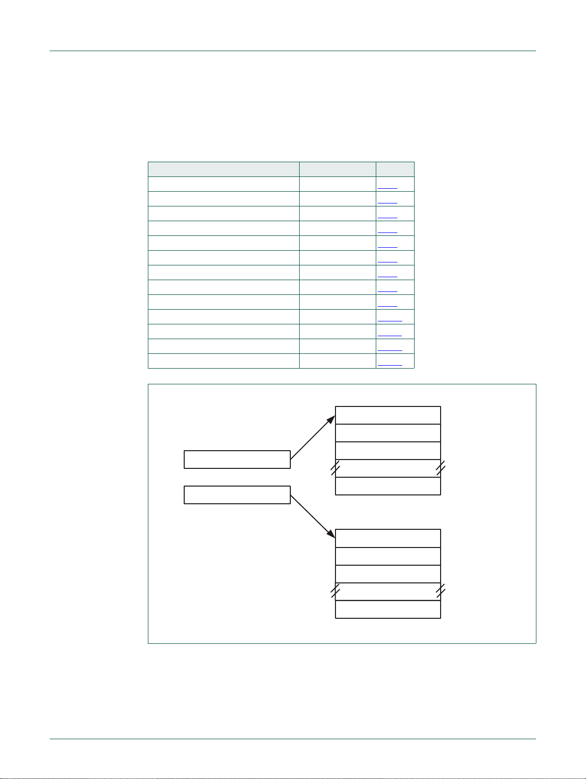
1.5 Block diagram
UM11029
Chapter 1: LPC84x Introductory information
Note: Yellow shaded blocks support general purpose DMA
Fig 1. LPC84x block diagram aaa-022793
UM11029 All information provided in this document is subject to legal disclaimers. © NXP Semiconductors N.V. 2017. All rights reserved.
User manual Rev. 1.0 — 16 June 2017 8 of 515
Page 9

UM11029
Chapter 2: LPC84x memory mapping
Rev. 1.0 — 16 June 2017 User manual
2.1 How to read this chapter
The memory mapping is identical for all LPC84x parts. Different LPC84x parts support
different flash and SRAM memory sizes.
2.2 General description
The LPC84x incorporates several distinct memory regions. Figure 2 shows the overall
map of the entire address space from the user program viewpoint following reset.
The APB peripheral area is 512 KB in size and is divided to allow for up to 32 peripherals.
Each peripheral is allocated 16 KB of space simplifying the address decoding.
The registers incorporated into the ARM Cortex-M0+ core, such as NVIC, SysTick, and
sleep mode control, are located on the private peripheral bus.
The GPIO port and pin interrupt/pattern match registers are accessed by the ARM
Cortex-M0+ single-cycle I/O enabled port (IOP).
UM11029 All information provided in this document is subject to legal disclaimers. © NXP Semiconductors N.V. 2017. All rights reserved.
User manual Rev. 1.0 — 16 June 2017 9 of 515
Page 10

NXP Semiconductors
2.2.1 Memory mapping
UM11029
Chapter 2: LPC84x memory mapping
Memory space
(reserved)
private peripheral bus
(reserved)
GPIO interrupts
GPIO
(reserved)
AHB
peripherals
(reserved)
APB
peripherals
(reserved)
RAM1
RAM0
(reserved)
Boot ROM
(reserved)
Flash memory
(up to 64 MB)
active interrupt vectors
0xFFFF FFFF
0xE010 0000
0xE000 0000
0xA008 0000
0xA004 0000
0xA000 0000
0x5001 4000
0x5000 0000
0x4008 0000
0x4000 0000
0x1000 4000
0x1000 2000
0x1000 0000
0x0F00 4000
0x0F00 0000
0x0001 0000
0x0000 0000
0x0000 00C0
0x0000 0000
AHB perpherals
MTB registers
DMA controller
SCTimer / PWM
31-30
29
28
27
26
25
24
23
22
21
20
19
18
17
16
15
14
13
12
11
10
9
8
7
6
5
4
3
2
1
0
(reserved)
CRC engine
APB perpherals
(reserved)
UART4
UART3
UART2
UART1
UART0
(reserved)
SPI1
SPI0
I2C1
I2C0
(reserved)
Syscon
IOCON
Flash controller
(reserved)
CTIMER 0
I2C3
I2C2
Input Multiplexing
(reserved)
Analog Comparator
PMU
ADC
DAC1
DAC0
(reserved)
Switch Matrix
Wake-up Timer
Multi-Rate Timer
Watchdog timer
0x5001 4000
0x5001 0000
0x5000 C000
0x5000 8000
0x5000 4000
0x5000 0000
0x4007 FFFF
0x4007 8000
0x4007 4000
0x4007 0000
0x4006 C000
0x4006 8000
0x4006 4000
0x4006 0000
0x4005 C000
0x4005 8000
0x4005 4000
0x4005 0000
0x4004 C000
0x4004 8000
0x4004 4000
0x4004 0000
0x4003 C000
0x4003 8000
0x4003 4000
0x4003 0000
0x4002 C000
0x4002 8000
0x4002 4000
0x4002 0000
0x4001 C000
0x4001 8000
0x4001 4000
0x4001 0000
0x4000 C000
0x4000 8000
0x4000 4000
0x4000 0000
aaa-027479
Fig 2. LPC84x Memory mapping
2.2.2 Micro Trace Buffer (MTB)
The LPC84x supports the ARM Cortex-M0+ Micro Trace Buffer. See Section 31.5.4.
UM11029 All information provided in this document is subject to legal disclaimers. © NXP Semiconductors N.V. 2017. All rights reserved.
User manual Rev. 1.0 — 16 June 2017 10 of 515
Page 11

UM11029
Chapter 3: LPC84x Boot Process
Rev. 1.0 — 16 June 2017 User manual
3.1 How to read this chapter
The bootloader is identical for all parts.
3.2 Features
• 16 KB on-chip boot ROM
• Contains the bootloader with In-System Programming (ISP) facility over multiple
peripheral communication (UART, I
– In-Application Programming (IAP) of flash memory.
– Integer divide routines.
– FAIM API.
– FRO API.
2
C, and SPI) and the following API:
3.3 Basic configuration
Depending on the FAIM configuration, the boot ROM sets the FRO control register to
select the operating frequency accordingly. If FAIM is not programmed or contains an
invalid value, the ROM begins at 12 MHz.
3.4 Pin description
When the ISP entry pin (PIO0_12) is pulled LOW on reset, the part enters ISP mode and
the ISP command handler starts up.
Table 3. Pin location in ISP mode
ISP mode Default FAIM configuration FAIM ISP selection
USART ISP PIO0_25 is UART0 TX
I2C ISP PIO0_11 is I2C0 SDA
SPI ISP PIO0_15 is SPI0 SCK
PIO0_24 is UART0 RX
Applicable when FAIM content
is invalid.
PIO0_10 is I2C0 SCL
Applicable when FAIM content
is invalid.
PIO0_22 is SPI0 SSEL0
PIO0_26 is SPI0 MISO
PIO0_27 is SPI0 MOSI
FAIM ISP pin
(FAIM word0, bit 30
and 31), Table 5
0x00 See: Table 6
0x01 -
0x02 See: Table 6
function (FAIM
word0, bit 30
and 31)
UM11029 All information provided in this document is subject to legal disclaimers. © NXP Semiconductors N.V. 2017. All rights reserved.
User manual Rev. 1.0 — 16 June 2017 11 of 515
Page 12

NXP Semiconductors
3.5 General description
3.5.1 Bootloader
The bootloader executes every time the device is powered on or reset. Based on the chip
configuration information, the bootloader controls initial operation after reset, including
setting internal voltage regulator, system clock, flash controller, miscellaneous factory
trimming value, and then allows programming and reprogramming of internal flash via a
set of commands on USART, I2C slave, or SPI slave bus. The LPC84x device must be
connected to a host system that provides the UART, I
UM11029
Chapter 3: LPC84x Boot Process
2
C or SPI master connections.
During the boot process, a LOW level after reset on the ISP pin is considered as an
external hardware request to start the ISP command handler via USART, I
interface. Otherwise, the bootloader checks if there is valid user code in flash. If the valid
user code is not found, the bootloader checks the FAIM configuration and enters one of
the ISP modes. Auto detect is selected if FAIM is invalid.
Remark: The sampling of pin the ISP entry pin can be disabled through programming
flash location 0x0000 02FC (see Section 4.3.6 “Code Read Protection (CRP)”
See Chapter 5 “
LPC84x ISP and IAP” for more details.
3.5.2 ROM-based APIs
Once the part has booted, the user can access several APIs located in the boot ROM. The
ROM API supports:
• Boot loader.
• Flash In-Application Programming (IAP).
• In-System Programming (ISP) through USART, SPI, and I
• On-chip ROM APIs for integer divide.
• FAIM API.
• FRO API.
2
C, or SPI
).
2
C.
The structure of the boot ROM APIs is shown in Figure 3
UM11029 All information provided in this document is subject to legal disclaimers. © NXP Semiconductors N.V. 2017. All rights reserved.
User manual Rev. 1.0 — 16 June 2017 12 of 515
.
Page 13

NXP Semiconductors
UM11029
Chapter 3: LPC84x Boot Process
+0x0
+0x4
+0x8
+0xC
+0x10
Ptr to IAP
0x0F001FF1
Ptr to ROM Driver table
0x0F001FF8
ROM Driver Table
Reserved
Reserved
Reserved
Clock setting and enter low power mode API
Pointer to 32-bit integer divide routines
…
Ptr to Device API Table n
IAP calls
Device API 3
Power profiles API function table
Device API 4
Integer Divide routines function table
Device API n
Ptr to Function 0
Ptr to Function 1
Ptr to Function 2
…
Ptr to Function n
Fig 3. Boot ROM structure
aaa-026624
UM11029 All information provided in this document is subject to legal disclaimers. © NXP Semiconductors N.V. 2017. All rights reserved.
User manual Rev. 1.0 — 16 June 2017 13 of 515
Page 14

NXP Semiconductors
The boot ROM structure should be included as follows:
typedef struct {
const uint32_t reserved0; /*!< Reserved */
const uint32_t reserved1; /*!< Reserved */
const uint32_t reserved2; /*!< Reserved */
const PWRD_API_T *pPWRD; /*!< Power API function table base address */
const ROM_DIV_API_T *divApiBase; /*!< Divider API function table base address */
} LPC_ROM_API_T;
#define ROM_DRIVER_BASE (0x0F001FF8)
Table 4. API calls
API Description Reference
Flash IAP Flash In-Application programming Table 37
Integer divider API 32-bit integer divide routines Table 471
3.6 Functional description
UM11029
Chapter 3: LPC84x Boot Process
3.6.1 Memory map after any reset
The boot ROM block is 16 KB in size. The boot block is located in the memory region
starting from address 0x0F00 0000. The bootloader is designed to run from this memory
area, but both the ISP and IAP software use parts of the on-chip RAM. The RAM usage is
described in Section 4.3.7 “ISP interrupt and SRAM use”
the boot block of the on-chip flash memory also become active after reset, i.e., the bottom
512 bytes of the boot block are also visible in the memory region starting from the address
0x0000 0000.
. The interrupt vectors residing in
UM11029 All information provided in this document is subject to legal disclaimers. © NXP Semiconductors N.V. 2017. All rights reserved.
User manual Rev. 1.0 — 16 June 2017 14 of 515
Page 15

NXP Semiconductors
3.6.2 Boot process
Reset
UM11029
Chapter 3: LPC84x Boot Process
CRP 1/2/3
enabled
yes
Device configure/
Initialize
WDT reset
no
No_ISP or
CRP3
enabled
yes
User code
valid
yes
A
no
Enable debugger
no
no
FAIM content invalid,
fixed USART/I2C/
SPI port pins
USART/I2S/
SPI ISP auto
detected
A
ISP pin
low
invalid
yes
no
FAIM content
valid or 0/1/2
FAIM ISP select 0,
USART port/pin
setting
UART ISP
no
yes
0/1/2
0
User code
valid
FAIM ISP select 0,
USART port/pin
setting
I2C ISP
yes
no
User code
21
FAIM ISP select 2,
SPI port/pin
setting
SPI ISP
USART ISP
command handler
I2C/SPI ISP
command handler
aaa-026887
Fig 4. Boot process flowchart
UM11029 All information provided in this document is subject to legal disclaimers. © NXP Semiconductors N.V. 2017. All rights reserved.
User manual Rev. 1.0 — 16 June 2017 15 of 515
Page 16

UM11029
Chapter 4: LPC84x FAIM
Rev. 1.0 — 16 June 2017 User manual
4.1 How to read this chapter
The Fast Initialization Memory (FAIM) is a 256-bit memory configured as eight words (or
rows) of 32-bits per word.
4.2 General description
The FAIM is a multiple time programmable (MTP), ultra low power memory, the full
contents of which are read and latched immediately after reset, with no clocks required.
The FAIM contents provide a user-programmable initial configuration for aspects of the
microcontroller, which take effect immediately after reset, before code begins to run. For
instance, the standard I/O pads normally come out of reset with the internal pull-ups
enabled. In some systems this may cause excess current to flow, until software can
reconfigure the pads. However, by programming the FAIM appropriately, every pad's reset
configuration can be customized. Other aspects which can be controlled by the FAIM are
initial FRO divider value (low power start), serial wire debug disable, default ISP interface
and pins, etc. One 32-bit FAIM row can be programmed, or read, using the ROM IAP calls
FAIMWrite and FAIMRead (see Chapter 5 “
LPC84x ISP and IAP” for details).
After a FAIMMWrite, a FAIMRead is required to update the output of the FAIM. Once a
read has been performed, the FAIM contents are visible in the AHB Peripheral address
space starting at 0x5001_0000.
For the pull-up, pull-down, and HI-Z IOCON pin configuration settings, a reset is needed
to transfer the newly programmed FAIM values into the IOCON pin configuration registers.
Executing a FAIMWrite followed by a FAIMRead does not update the current configuration
in the IOCON pin configuration registers. Only a reset can do so. Software can at any time
rewrite the IOCON pin configuration. Similarly, for SWD Disable, Low Power Start
configuration, ISP interface and pin select, a reset is needed to update the actual startup
configuration.
The FAIM is limited to 200 program cycles, so care must be taken to write this memory
only when necessary during an end-product's development. Also, the FAIM programming
voltage range is 3.0 V Vdd 3.6 V.
Remark: If internal pull-down is enabled via FAIM on the ISP pin (PIO0_12) or the reset
pin (PIO0_5), ensure to have a strong external pull-up to avoid going into ISP mode or into
reset after boot-up.
4.2.1 FAIM bit definitions
The functions of FAIM bits are described in the following tables.
UM11029 All information provided in this document is subject to legal disclaimers. © NXP Semiconductors N.V. 2017. All rights reserved.
User manual Rev. 1.0 — 16 June 2017 16 of 515
Page 17

NXP Semiconductors
Table 5. FAIM word 0 bit description
Bit Description Default value
0 SWD disable 0
1 Low Power Boot 0
26:2 Reserved 0
28 Reserved 0
29, 27 FAIM content valid bits 11
31:30 ISP interface select 0
UM11029
Chapter 4: LPC84x FA IM
0 SWD enabled
1 SWD disabled
0 Normal boot (12 MHz)
1 Low Power Boot (1.5 MHz)
00 FAIM content invalid
01 FAIM content invalid
10 FAIM content invalid
11 FAIM content valid
00 USART0
01 I2C0
10 SPI0
11 Reserved
Table 6. FAIM word 1 bit description
Bit Description Default value
4:0 ISP Rx pin select (USART0 Rx, SPI MOSI) 0x18
0x0
0x1
...
0x1F
PIOn_0
PIOn_1
...
PIOn_31
7:5 ISP Rx port select (USART0 Rx, SPI MOSI) 0
0x0 Port 0
0x1 Port 1
12:8 ISP Tx pin select (USART0 Tx, SPI MISO) 0x19
0x0
0x1
...
0x1F
PIOn_0
PIOn_1
...
PIOn_31
15:13 ISP Tx port select (USART0 Tx, SPI MISO) 0
0x0 Port 0
0x1 Port 1
20:16 ISP clock pin select (SPI SCK) 0
0x0
0x1
...
0x1F
PIOnPIOn_0
PIOn_1
...
PIOn_31
UM11029 All information provided in this document is subject to legal disclaimers. © NXP Semiconductors N.V. 2017. All rights reserved.
User manual Rev. 1.0 — 16 June 2017 17 of 515
Page 18

NXP Semiconductors
Table 6. FAIM word 1 bit description
Bit Description Default value
23:21 ISP clock port select (SPI SCK) 0
28:24 ISP SPI0 SSELN0 pin select 0
31:29 ISP SPI0 SSELN0 port select 0
Table 7. FAIM word 2 bit description
Bit Description Default value
31:0 Reserved 0
0x0 Port 0
0x1 Port 1
0x0
0x1
...
0x1F
PIOn_0
PIOn_1
...
PIOn_31
0x0 Port 0
0x1 Port 1
UM11029
Chapter 4: LPC84x FA IM
Table 8. FAIM word 3 bit description
Bit Description Default value
31:0 Reserved 0
Table 9. FAIM word 4 bit description
Bit Description Default value
19:0 Reserved 0
21:20 PIO1_21 0x2
0x0 Hi-Z
0x1 Pull-down
0x2 Pull-up
0x3 Repeater
23:22 PIO1_20. See description of bits of bits 21:20. 0x2
25:24 PIO1_19. See description of bits 21:20. 0x2
27:26 PIO1_18. See description of bits 21:20. 0x2
29:28 PIO1_17. See description of bits 21:20. 0x2
31:30 PIO1_16. See description of bits 21:20. 0x2
Table 10. FAIM word 5 bit description
Bit Description Default value
1:0 PIO1_15
0x0 Hi-Z 0x2
0x1 Pull-down
0x2 Pull-up
0x3 Repeater
3:2 PIO1_14. See description of bits 1:0. 0x2
UM11029 All information provided in this document is subject to legal disclaimers. © NXP Semiconductors N.V. 2017. All rights reserved.
User manual Rev. 1.0 — 16 June 2017 18 of 515
Page 19

NXP Semiconductors
Table 10. FAIM word 5 bit description
Bit Description Default value
5:4 PIO1_13. See description of bits 1:0. 0x2
7:6 PIO1_12. See description of bits 1:0. 0x2
9:8 PIO1_11. See description of bits 1:0. 0x2
11:10 PIO1_10. See description of bits 1:0. 0x2
13:12 PIO1_9. See description of bits 1:0. 0x2
15:14 PIO1_8. See description of bits 1:0. 0x2
17:16 PIO1_7. See description of bits 1:0. 0x2
19:18 PIO1_6. See description of bits 1:0. 0x2
21:20 PIO1_5. See description of bits 1:0. 0x2
23:22 PIO1_4. See description of bits 1:0. 0x2
25:24 PIO1_3. See description of bits 1:0. 0x2
27:26 PIO1_2. See description of bits 1:0. 0x2
29:28 PIO1_1. See description of bits 1:0. 0x2
31:30 PIO1_0. See description of bits 1:0. 0x2
UM11029
Chapter 4: LPC84x FA IM
Table 11. FAIM word 6 bit description
Bit Description Default value
1:0 PIO0_31 0
0x0 Hi-Z 0x2
0x1 Pull-down
0x2 Pull-up
0x3 Repeater
3:2 PIO0_30. See description of bits 1:0. 0x2
5:4 PIO0_29. See description of bits 1:0. 0x2
7:6 PIO0_28. See description of bits 1:0. 0x2
9:8 PIO0_27. See description of bits 1:0. 0x2
11:10 PIO0_26. See description of bits 1:0. 0x2
13:12 PIO0_25. See description of bits 1:0. 0x2
15:14 PIO0_24. See description of bits 1:0. 0x2
17:16 PIO0_23. See description of bits 1:0. 0x2
19:18 PIO0_22. See description of bits 1:0. 0x2
21:20 PIO0_21. See description of bits 1:0. 0x2
23:22 PIO0_20. See description of bits 1:0. 0x2
25:24 PIO0_19. See description of bits 1:0. 0x2
27:26 PIO0_18. See description of bits 1:0. 0x2
29:28 PIO0_17. See description of bits 1:0. 0x2
31:30 PIO0_16. See description of bits 1:0. 0x2
UM11029 All information provided in this document is subject to legal disclaimers. © NXP Semiconductors N.V. 2017. All rights reserved.
User manual Rev. 1.0 — 16 June 2017 19 of 515
Page 20

NXP Semiconductors
Table 12. FAIM word 7 bit description
Bit Description Default value
1:0 PIO0_15 0
3:2 PIO0_14. See description of bits 1:0. 0x2
5:4 PIO0_13. See description of bits 1:0. 0x2
7:6 PIO0_12. See description of bits 1:0. 0x2
9:8 PIO0_11. See description of bits 1:0. 0x2
11:10 PIO0_10. See description of bits 1:0. 0x2
13:12 PIO0_9. See description of bits 1:0. 0x2
15:14 PIO0_8. See description of bits 1:0. 0x2
17:16 PIO0_7. See description of bits 1:0. 0x2
19:18 PIO0_6. See description of bits 1:0. 0x2
21:20 PIO0_5. See description of bits 1:0. 0x2
23:22 PIO0_4. See description of bits 1:0. 0x2
25:24 PIO0_3. See description of bits 1:0. 0x2
27:26 PIO0_2. See description of bits 1:0. 0x2
29:28 PIO0_1. See description of bits 1:0. 0x2
31:30 PIO0_0. See description of bits 1:0. 0x2
UM11029
Chapter 4: LPC84x FA IM
0x0 Hi-Z 0x2
0x1 Pull-down
0x2 Pull-up
0x3 Repeater
UM11029 All information provided in this document is subject to legal disclaimers. © NXP Semiconductors N.V. 2017. All rights reserved.
User manual Rev. 1.0 — 16 June 2017 20 of 515
Page 21

UM11029
Chapter 5: LPC84x ISP and IAP
Rev. 1.0 — 16 June 2017 User manual
5.1 How to read this chapter
All LPC84x devices include ROM-based services for programming and reading the flash
memory in addition to other functions. In-System Programming works on an
unprogrammed or previously programmed device using one from a selection of hardware
interfaces. In-Application Programming allows application software to do the same kinds
of operations.
See specific device data sheets for different flash configurations.
Remark: In addition to the ISP and IAP commands, the flash configuration register
(FLASHCFG) can be accessed in the flash controller block to configure flash memory
access times, see Section 6.4.1
5.2 Features
.
• In-System Programming: In-System programming (ISP) is programming or
reprogramming the on-chip flash memory, using the boot loader software and USART,
2
I
C, or SPI serial port. This can be done when the part resides in the end-user board.
• In Application Programming: In-Application (IAP) programming is performing erase
and write operation on the on-chip flash memory, as directed by the end-user
application code.
• Flexible ISP mode and port pin selection through FAIM memory configuration.
• Small size (64 byte) page erase programming.
5.3 General description
5.3.1 Boot loader
For the boot loader operation and boot pin, see Chapter 3 “LPC84x Boot Process”.
The boot loader version can be read by ISP/IAP calls (see Section 5.5.13
Section 5.6.6
5.3.2 Memory map after any reset
The boot ROM is located in the memory region starting from the address 0x0F00 0000.
The boot loader is designed to run from this memory area, but both the ISP and IAP
software use parts of the on-chip RAM. The RAM usage is described later in
Section 5.3.7
or
).
.
UM11029 All information provided in this document is subject to legal disclaimers. © NXP B.V. 2017. All rights reserved.
User manual Rev. 1.0 — 16 June 2017 21 of 515
Page 22

NXP Semiconductors
5.3.3 Flash content protection mechanism
The LPC84x is equipped with the Error Correction Code (ECC) capable Flash memory.
The purpose of an error correction module is twofold. Firstly, it decodes data words read
from the memory into output data words. Secondly, it encodes data words to be written to
the memory. The error correction capability consists of single bit error correction with
Hamming code.
The operation of the ECC is transparent to the running application. The ECC content itself
is stored in a flash memory not accessible by the user’s code to either read from it or write
into it on its own. Six bits of ECC corresponds to every consecutive 32 bit of the user
accessible Flash. Consequently, Flash bytes from 0x0000 0000 to 0x0000 0003 are
protected by the first 6-bit ECC, Flash bytes from 0x0000 0004 to 0x0000 0007 are
protected by the second 6-bit ECC byte, etc.
Whenever the CPU requests a read from user’s Flash, both 32 bits of raw data containing
the specified memory location and the matching ECC byte are evaluated. If the ECC
mechanism detects a single error in the fetched data, a correction will be applied before
data are provided to the CPU. When a write request into the user’s Flash is made, write of
user specified content is accompanied by a matching ECC value calculated and stored in
the ECC memory.
UM11029
Chapter 5: LPC84x ISP and IAP
When a sector of Flash memory is erased, the corresponding ECC bytes are also erased.
Once an ECC byte is written, it can not be updated unless it is erased first. Therefore, for
the implemented ECC mechanism to perform properly, data must be written into the flash
memory in groups of 4 bytes (or multiples of 4), aligned as described above.
5.3.4 Criteria for Valid User Code
The reserved CPU exception vector location 7 (offset 0x0000 001C in the vector table)
should contain the 2’s complement of the check-sum of table entries 0 through 6. This
causes the checksum of the first 8 table entries to be 0. The boot loader code checksums
the first 8 locations in sector 0 of the flash.
If the checksum is not zero indicating valid user code is not found, the bootloader will
check the FAIM configuration and enter UART/I2C/SPI ISP mode automatically.
5.3.5 Flash partitions
Some IAP and ISP commands operate on sectors and specify sector numbers. In
addition, a page erase command is available. The size of a sector is 1 KB and the size of
a page is 64 Byte. One sector contains 16 pages.
Table 13. LPC82x flash configuration <tbd>
Sector
number
0 1 0 -15 0x0000 0000 - 0x0000 03FF yes yes
1 1 16 - 31 0x0000 0400 - 0x0000 07FF yes yes
2 1 32 - 47 0x0000 0800 - 0x0000 0BFF yes yes
3 1 48 - 63 0x0000 0C00 - 0x0000 0FFF yes yes
4 1 64 - 79 0x0000 1000 - 0x0000 13FF yes yes
5 1 80 - 95 0x0000 1400 - 0x0000 17FF yes yes
Sector
size [KB]
Page number Address range 16 KB
flash
32 KB
flash
UM11029 All information provided in this document is subject to legal disclaimers. © NXP B.V. 2017. All rights reserved.
User manual Rev. 1.0 — 16 June 2017 22 of 515
Page 23

NXP Semiconductors
Table 13. LPC82x flash configuration <tbd>
Sector
number
6 1 96 - 111 0x0000 1800 - 0x0000 1BFF yes yes
7 1 112 - 127 0x0000 1C00 - 0x0000 1FFF yes yes
8 1 128 - 143 0x0000 2000 - 0x0000 23FF yes yes
9 1 144 - 159 0x0000 2400 - 0x0000 27FF yes yes
10 1 160 - 175 0x0000 2800 - 0x0000 2BFF yes yes
11 1 176 - 191 0x0000 2C00 - 0x0000 2FFF yes yes
12 1 192 - 207 0x0000 3000 - 0x0000 33FF yes yes
13 1 208 - 223 0x0000 3400 - 0x0000 37FF yes yes
14 1 224 - 239 0x0000 3800 - 0x0000 3BFF yes yes
15 1 240 - 255 0x0000 3C00 - 0x0000 3FFF yes yes
16 1 256 - 271 0x0000 4000 - 0x0000 43FF - yes
17 1 272 - 287 0x0000 4400 - 0x0000 47FF - yes
18 1 288 - 303 0x0000 4800 - 0x0000 4BFF - yes
19 1 304 - 319 0x0000 4C00 - 0x0000 4FFF - yes
20 1 320 - 335 0x0000 5000 - 0x0000 53FF - yes
21 1 336 - 351 0x0000 5400 - 0x0000 57FF - yes
22 1 352 - 367 0x0000 5800 - 0x0000 5BFF - yes
23 1 368 - 383 0x0000 5C00 - 0x0000 5FFF - yes
24 1 384 - 399 0x0000 6000 - 0x0000 63FF - yes
25 1 400 - 415 0x0000 6400 - 0x0000 67FF - yes
26 1 416 - 431 0x0000 6800 - 0x0000 6BFF - yes
27 1 432 - 447 0x0000 6C00 - 0x0000 6FFF - yes
28 1 448 - 463 0x0000 7000 - 0x0000 73FF - yes
29 1 464 - 479 0x0000 7400 - 0x0000 77FF - yes
30 1 480 - 495 0x0000 7800 - 0x0000 7BFF - yes
31 1 496 - 511 0x0000 7C00 - 0x0000 7FFF - yes
Sector
size [KB]
UM11029
Chapter 5: LPC84x ISP and IAP
Page number Address range 16 KB
flash
32 KB
flash
5.3.6 Code Read Protection (CRP)
Code Read Protection is a mechanism that allows the user to enable different levels of
security in the system so that access to the on-chip flash and use of the ISP can be
restricted. When needed, CRP is invoked by programming a specific pattern in the flash
image at offset 0x0000 02FC. IAP commands are not affected by the code read
protection.
Table 1 shows the limitations of the USART ISP commands when CRP (CRP1, CRP2, or
CRP3) is enabled.
Note: Any CRP change becomes effective only after the device has gone through a
power cycle.
UM11029 All information provided in this document is subject to legal disclaimers. © NXP B.V. 2017. All rights reserved.
User manual Rev. 1.0 — 16 June 2017 23 of 515
Page 24

NXP Semiconductors
UM11029
Chapter 5: LPC84x ISP and IAP
Table 14. USART ISP command limitations in CRP modes
Name Pattern programmed
in 0x0000 02FC
NO_ISP 0x4E69 7370 Prevents sampling of the pins for entering ISP mode. ISP sampling pin is available for
CRP1 0x1234 5678 Access to chip via the SWD pins is disabled. This mode allows partial flash update using
Description
other applications.
the following USART ISP commands and restrictions:
• Write to RAM command cannot access RAM below 0x1000 0600. Access to
addresses below 0x1000 0600 is disabled.
• Copy RAM to flash command cannot write to Sector 0.
• Erase command can erase Sector 0 only when all sectors are selected for erase.
• Compare command is disabled.
• Read Memory command is disabled.
This mode is useful when CRP is required and flash field updates are needed but all
sectors can not be erased. Since compare command is disabled in case of partial
updates the secondary loader should implement checksum mechanism to verify the
integrity of the flash.
CRP2 0x8765 4321 Access to chip via the SWD pins is disabled. The following ISP commands are disabled:
• Read Memory
• Write to RAM
• Go
• Copy RAM to flash
• Compare
When CRP2 is enabled the ISP erase command only allows erasure of all user sectors.
CRP3 0x4321 8765 Access to chip via the SWD pins is disabled. ISP entry selected via the ISP entry pin is
disabled if a valid user code is present in flash sector 0.
This mode effectively disables ISP override using the entry pin. It is up to the application
of the user to provide a flash update mechanism using IAP calls or call reinvoke ISP
command to enable flash update via USART.
Caution: If CRP3 is selected, no future factory testing can be performed on the
device.
In case a CRP mode is enabled and access to the chip is allowed via the ISP, an
unsupported or restricted ISP command will be terminated with return code
CODE_READ_PROTECTION_ENABLED.
5.3.6.1 ISP entry protection
In addition to the three CRP modes, the user can prevent the sampling of the pin for
entering ISP mode and thereby release the pin for other applications. This is called the
NO_ISP mode. The NO_ISP mode can be entered by programming the pattern
0x4E69 7370 at location 0x0000 02FC.
The NO_ISP mode is identical to the CRP3 mode except for SWD access, which is
allowed in NO_ISP mode but disabled in CRP3 mode. The NO_ISP mode does not offer
any code protection.
5.3.6.2 ISP entry configuration and detection
The LPC84x UART/I2C/SPI ISP mode allows programming and reprogramming of the
internal FLASH via a set of commands on the UART, I2C slave, or SPI slave buses. Two
bits of the FAIM flash are used for ISP mode selection.
UM11029 All information provided in this document is subject to legal disclaimers. © NXP B.V. 2017. All rights reserved.
User manual Rev. 1.0 — 16 June 2017 24 of 515
Page 25

NXP Semiconductors
If FAIM content is invalid, the default ISP selection is USART/I2C/SPI or auto detection
mode. In auto detection mode, the LPC84x enables all three interfaces on the fixed GPIO
port and pins, and selects the first one that has either a successful auto baud detection on
USART or a valid probe message response on I2C or SPI.
If FAIM content is valid, USART, I2C, or SPI ISP mode is configured in the FAIM.
Additional SWM configuration for the interface and pins through FAIM is required. For
example, if FAIM ISP selection is 0x02, the GPIO port and pin information for SPI0, such
as SSEL, SCK, MOSI, and MISO is provided by the FAIM. The boot ROM reads the GPIO
port and pin information from the FAIM and writes to the SWM and IOCON registers
accordingly as part of the SPI initialization.
5.3.7 ISP interrupt and SRAM use
5.3.7.1 Interrupts during IAP
The on-chip flash memory is not accessible during erase/write operations. When the user
application code starts executing, the interrupt vectors from the user flash area are active.
Before making any IAP call, either disable the interrupts or ensure that the user interrupt
vectors are active in RAM and that the interrupt handlers reside in RAM. The IAP code
does not use or disable interrupts.
UM11029
Chapter 5: LPC84x ISP and IAP
5.3.7.2 RAM used by ISP command handlers
The stack of UART ISP commands is located at address 0x1000 0600. The maximum
stack usage is 1280 bytes (0x500) and grows downwards.
The DMA is used by the SPI ISP mode. The DMA descriptor table location is located at
address 0x1000 0600. The DMA table size is 512 bytes (0x200) and grows upwards.
Therefore, depending on the ISP mode entered, the maximum RAM used by ISP mode is
2 K starting from the address 0x1000 0000.
Memory for the USART and I2C/SPI ISP commands is allocated dynamically.
UM11029 All information provided in this document is subject to legal disclaimers. © NXP B.V. 2017. All rights reserved.
User manual Rev. 1.0 — 16 June 2017 25 of 515
Page 26

NXP Semiconductors
5.4 USART ISP communication protocol
All USART ISP commands should be sent as single ASCII strings. Strings should be
terminated with Carriage Return (CR) and/or Line Feed (LF) control characters. Extra
<CR> and <LF> characters are ignored. All ISP responses are sent as <CR><LF>
terminated ASCII strings. Data is sent and received in plain binary format.
5.4.1 USART ISP initialization
Once the USART ISP mode is entered, the auto-baud routine needs to synchronize with
the host via the serial port (USART).
The host should send a ’?’ (0x3F) as a synchronization character and wait for a response.
The host side serial port settings should be 8 data bits, 1 stop bit and no parity. The
auto-baud routine measures the bit time of the received synchronization character in
terms of its own frequency and programs the baud rate generator of the serial port. It also
sends an ASCII string ("Synchronized<CR><LF>") to the host. In response to this, the
host should send back the same string ("Synchronized<CR><LF>").
The auto-baud routine looks at the received characters to verify synchronization. If
synchronization is verified then "OK<CR><LF>" string is sent to the host. The host should
respond by sending the crystal frequency (in kHz) at which the part is running. The
response is required for backward compatibility of the boot loader code and is ignored.
"OK<CR><LF>" string is sent to the host after receiving the crystal frequency. If
synchronization is not verified then the auto-baud routine waits again for a
synchronization character. In USART ISP mode, the part is clocked by the FAIM
configuration and the crystal frequency is ignored.
UM11029
Chapter 5: LPC84x ISP and IAP
Once the crystal frequency is received the part is initialized and the ISP command handler
is invoked. For safety reasons an "Unlock" command is required before executing the
commands resulting in flash erase/write operations and the "Go" command. The rest of
the commands can be executed without the unlock command. The Unlock command is
required to be executed once per ISP session. The Unlock command is explained in
Section 5.5 “
USART ISP commands”.
5.4.2 USART ISP command format
"Command Parameter_0 Parameter_1 ... Parameter_n<CR><LF>" "Data" (Data only for
Write commands).
5.4.3 USART ISP response format
"Return_Code<CR><LF>Response_0<CR><LF>Response_1<CR><LF> ...
Response_n<CR><LF>" "Data" (Data only for Read commands).
5.4.4 USART ISP data format
The data stream is in plain binary format.
UM11029 All information provided in this document is subject to legal disclaimers. © NXP B.V. 2017. All rights reserved.
User manual Rev. 1.0 — 16 June 2017 26 of 515
Page 27

NXP Semiconductors
Chapter 5: LPC84x ISP and IAP
5.5 USART ISP commands
The following commands are accepted by the ISP command handler. Detailed status
codes are supported for each command. The command handler sends the return code
INVALID_COMMAND when an undefined command is received. Commands and return
codes are in ASCII format.
CMD_SUCCESS is sent by ISP command handler only when received ISP command has
been completely executed and the new ISP command can be given by the host.
Exceptions from this rule are "Set Baud Rate", "Write to RAM", "Read Memory", and "Go"
commands.
Table 15. USART ISP command summary
ISP Command Usage Section
Unlock U <Unlock Code> 5.5.1
Set Baud Rate B <Baud Rate> <stop bit> 5.5.2
Echo A <setting> 5.5.3
Write to RAM W <start address> <number of bytes> 5.5.4
Read Memory R <address> <number of bytes> 5.5.5
Prepare sectors for write operation P <start sector number> <end sector number> 5.5.6
Copy RAM to flash C <Flash address> <RAM address> <number of bytes> 5.5.7
Go G <address> <Mode> 5.5.8
Erase sector(s) E <start sector number> <end sector number> 5.5.9
Erase page(s) X <start page number> <end page number> 5.5.10
Blank check sector(s) I <start sector number> <end sector number> 5.5.11
Read Part ID J 5.5.12
Read Boot code version K 5.5.13
Compare M <address1> <address2> <number of bytes> 5.5.14
ReadUID N 5.5.15
Read CRC checksum S <address> <number of bytes> 5.5.16
Read flash signature Z 5.5.17
Read/Write FAIM Page O 5.5.18
UM11029
Ta bl e 1 6 lists the supported USART ISP commands for each CRP level.
Table 16. ISP commands allowed for different CRP levels
ISP command CRP1 CRP2 CRP3 (no entry in
Unlock yes yes n/a
Set Baud Rate yes yes n/a
Echo yes yes n/a
Write to RAM yes; above 0x1000 0600 only no n/a
Read Memory no no n/a
Prepare sectors for write operation yes yes n/a
Copy RAM to flash yes; not to sector 0 no n/a
Go no no n/a
UM11029 All information provided in this document is subject to legal disclaimers. © NXP B.V. 2017. All rights reserved.
User manual Rev. 1.0 — 16 June 2017 27 of 515
ISP mode allowed)
Page 28

NXP Semiconductors
UM11029
Chapter 5: LPC84x ISP and IAP
Table 16. ISP commands allowed for different CRP levels
ISP command CRP1 CRP2 CRP3 (no entry in
ISP mode allowed)
Erase sector(s) yes; sector 0 can only be erased when all
sectors are erased.
Erase page(s) yes; page 0 can only be erased when all
pages are erased (not recommended, use
Erase Sector).
Blank check sectors no no n/a
Read Part ID yes yes n/a
Read Boot code version yes yes n/a
Compare no no n/a
ReadUID yes yes n/a
Read CRC no no n/a
Read flash signature yes (full range of the flash only) no n/a
Read/Write FAIM page yes yes n/a
yes; all sectors only n/a
yes; all pages only n/a
5.5.1 Unlock
Table 17. USART ISP Unlock command
Command U
Input Unlock code: 23130
Return Code CMD_SUCCESS |
INVALID_CODE |
PARAM_ERROR
Description This command is used to unlock Flash Write, Erase, and Go commands.
Example "U 23130<CR><LF>" unlocks the Flash Write/Erase & Go commands.
10
5.5.2 Set Baud Rate
Table 18. USART ISP Set Baud Rate command
Command B
Input Baud Rate, FAIM configuration dependant: 9600 | 19200 | 38400 | 57600 | 115200 | 230400 | 460800
Stop bit: 1 | 2
Return Code CMD_SUCCESS |
INVALID_BAUD_RATE |
INVALID_STOP_BIT |
PARAM_ERROR
Description This command is used to change the baud rate. The new baud rate is effective after the command handler
sends the CMD_SUCCESS return code.
Example "B 57600 1<CR><LF>" sets the serial port to baud rate 57600 bps and 1 stop bit.
UM11029 All information provided in this document is subject to legal disclaimers. © NXP B.V. 2017. All rights reserved.
User manual Rev. 1.0 — 16 June 2017 28 of 515
Page 29

NXP Semiconductors
UM11029
Chapter 5: LPC84x ISP and IAP
5.5.3 Echo
Table 19. USART ISP Echo command
Command A
Input Setting: ON = 1 | OFF = 0
Return Code CMD_SUCCESS |
PARAM_ERROR
Description The default setting for echo command is ON. When ON the ISP command handler sends the received serial
data back to the host.
Example "A 0<CR><LF>" turns echo off.
5.5.4 Write to RAM
The host should send the plain binary code after receiving the CMD_SUCCESS return
code. This ISP command handler responds with “OK<CR><LF>” when the transfer has
finished.
Table 20. USART ISP Write to RAM command
Command W
Input Start Address: RAM address where data bytes are to be written. This address should be a word boundary.
Number of Bytes: Number of bytes to be written. Count should be a multiple of 4
Return Code CMD_SUCCESS |
ADDR_ERROR (Address not on word boundary) |
ADDR_NOT_MAPPED |
COUNT_ERROR (Byte count is not multiple of 4) |
PARAM_ERROR |
CODE_READ_PROTECTION_ENABLED
Description This command is used to download data to RAM. This command is blocked when code read protection
levels 2 or 3 are enabled. Writing to addresses below 0x1000 0600 is disabled for CRP1.
Example "W 268437504 4<CR><LF>" writes 4 bytes of data to address 0x1000 0800.
5.5.5 Read Memory
Reads the plain binary code of the data stream, followed by the CMD_SUCCESS return
code.
Table 21. USART ISP Read Memory command
Command R
Input Start Address: Address from where data bytes are to be read. This address should be a word boundary.
Number of Bytes: Number of bytes to be read. Count should be a multiple of 4.
Return Code CMD_SUCCESS followed by <actual data (plain binary)> |
ADDR_ERROR (Address not on word boundary) |
ADDR_NOT_MAPPED |
COUNT_ERROR (Byte count is not a multiple of 4) |
PARAM_ERROR |
CODE_READ_PROTECTION_ENABLED
Description This command is used to read data from RAM or flash memory. This command is blocked when code read
protection is enabled.
Example "R 268437504 4<CR><LF>" reads 4 bytes of data from address 0x1000 0800.
UM11029 All information provided in this document is subject to legal disclaimers. © NXP B.V. 2017. All rights reserved.
User manual Rev. 1.0 — 16 June 2017 29 of 515
Page 30

NXP Semiconductors
UM11029
Chapter 5: LPC84x ISP and IAP
5.5.6 Prepare sectors for write operation
This command makes flash write/erase operation a two-step process.
Table 22. USART ISP Prepare sectors for write operation command
Command P
Input Star t Sec t o r Num b er
End Sector Number: Should be greater than or equal to start sector number.
Return Code CMD_SUCCESS |
BUSY |
INVALID_SECTOR |
PARAM_ERROR
Description This command must be executed before executing "Copy RAM to flash" or "Erase Sector(s)", or “Erase
Pages” command. Successful execution of the "Copy RAM to flash" or "Erase Sector(s)" or “Erase Pages”
command causes relevant sectors to be protected again. To prepare a single sector use the same "Start"
and "End" sector numbers.
Example "P 0 0<CR><LF>" prepares the flash sector 0.
5.5.7 Copy RAM to flash
When writing to the flash, the following limitations apply:
1. The smallest amount of data that can be written to flash by the copy RAM to flash
command is 64 byte (equal to one page).
2. One page consists of 16 flash words (lines), and the smallest amount that can be
modified per flash write is one flash word (one line). This limitation exists because
ECC is applied during the flash write operation, see Section 5.3.3
.
3. To avoid write disturbance (a mechanism intrinsic to flash memories), an erase
should be performed after 16 consecutive writes inside the same page. Note that the
erase operation then erases the entire sector.
Remark: Once a page has been written to 16 times, it is still possible to write to other
pages within the same sector without performing a sector erase (assuming that those
pages have been erased previously).
UM11029 All information provided in this document is subject to legal disclaimers. © NXP B.V. 2017. All rights reserved.
User manual Rev. 1.0 — 16 June 2017 30 of 515
Page 31

NXP Semiconductors
UM11029
Chapter 5: LPC84x ISP and IAP
Table 23. USART ISP Copy command
Command C
Input Flash Address(DST): Destination flash address where data bytes are to be written. The destination address
should be a 64 byte boundary.
RAM Address(SRC): Source RAM address from where data bytes are to be read.
Number of Bytes: Number of bytes to be written. Should be 64 | 128 | 256 | 512 | 1024
Return Code CMD_SUCCESS |
SRC_ADDR_ERROR (Address not on word boundary) |
DST_ADDR_ERROR (Address not on correct boundary) |
SRC_ADDR_NOT_MAPPED |
DST_ADDR_NOT_MAPPED |
COUNT_ERROR (Byte count is not 64 | 128 | 256 | 512 | 1024) |
SECTOR_NOT_PREPARED_FOR WRITE_OPERATION |
BUSY |
CMD_LOCKED |
PARAM_ERROR |
CODE_READ_PROTECTION_ENABLED
Description This command is used to program the flash memory. The "Prepare Sector(s) for Write Operation" command
should precede this command. The affected sectors are automatically protected again once the copy
command is successfully executed. This command is blocked when code read protection is enabled. Also see
Section 5.3.3
for the number of bytes that can be written.
Example "C 0 268437504 512<CR><LF>" copies 512 bytes from the RAM address 0x1000 0800 to the flash address
0.
5.5.8 Go
Table 24. USART ISP Go command
Command G
Input Address: Flash or RAM address from which the code execution is to be started. This address should be on
a word boundary.
Mode: T (Execute program in Thumb Mode) |
Return Code CMD_SUCCESS |
ADDR_ERROR |
ADDR_NOT_MAPPED |
CMD_LOCKED |
PARAM_ERROR |
CODE_READ_PROTECTION_ENABLED
Description This command is used to execute a program residing in RAM or flash memory. It may not be possible to
return to the ISP command handler once this command is successfully executed. This command is blocked
when code read protection is enabled.
Example "G 0 T<CR><LF>" branches to address 0x0000 0000 in Thumb mode only.
UM11029 All information provided in this document is subject to legal disclaimers. © NXP B.V. 2017. All rights reserved.
User manual Rev. 1.0 — 16 June 2017 31 of 515
Page 32

NXP Semiconductors
UM11029
Chapter 5: LPC84x ISP and IAP
5.5.9 Erase sectors
Table 25. USART ISP Erase sector command
Command E
Input Star t Sec t o r Num b er
End Sector Number: Should be greater than or equal to start sector number.
Return Code CMD_SUCCESS |
BUSY |
INVALID_SECTOR |
SECTOR_NOT_PREPARED_FOR_WRITE_OPERATION |
CMD_LOCKED |
PARAM_ERROR |
CODE_READ_PROTECTION_ENABLED
Description This command is used to erase one or more sector(s) of on-chip flash memory. This command only allows
erasure of all user sectors when the code read protection is enabled.
Example "E 2 3<CR><LF>" erases the flash sectors 2 and 3.
5.5.10 Erase pages
Table 26. USART ISP Erase page command
Command X
Input Star t Page Number
End Page Number: Should be greater than or equal to start page number.
Return Code CMD_SUCCESS |
BUSY |
INVA L I D _ PAGE |
SECTOR_NOT_PREPARED_FOR_WRITE_OPERATION |
CMD_LOCKED |
PARAM_ERROR |
CODE_READ_PROTECTION_ENABLED
Description This command is used to erase one or more page(s) of on-chip flash memory.
Example "X 2 3<CR><LF>" erases the flash pages 2 and 3.
5.5.11 Blank check sectors
Table 27. USART ISP Blank check sector command
Command I
Input Star t Sec t o r Num b er :
End Sector Number: Should be greater than or equal to start sector number.
Return Code CMD_SUCCESS |
SECTOR_NOT_BLANK (followed by <Offset of the first non blank word location> <Contents of non blank
word location>) |
INVALID_SECTOR |
PARAM_ERROR
Description This command is used to blank check one or more sectors of on-chip flash memory.
Example "I 2 3<CR><LF>" blank checks the flash sectors 2 and 3.
UM11029 All information provided in this document is subject to legal disclaimers. © NXP B.V. 2017. All rights reserved.
User manual Rev. 1.0 — 16 June 2017 32 of 515
Page 33

NXP Semiconductors
5.5.12 Read Part Identification number
Table 28. USART ISP Read Part Identification command
Command J
Input None.
Return Code CMD_SUCCESS followed by part identification number (see Ta bl e 2 9
Description This command is used to read the part identification number.
Table 29. LPC84x device ID register values
Part number Part ID
LPC844M201JBD48 0x00008442
LPC844M201JBD64 0x00008441
LPC844M201JHI33 0x00008444
LPC844M201JHI48 0x00008442
LPC845M301JBD48 0x00008452
LPC845M301JBD64 0x00008451
LPC845M301JHI33 0x00008454
LPC845M301JHI48 0x00008453
UM11029
Chapter 5: LPC84x ISP and IAP
).
5.5.13 Read Boot code version number
Table 30. USART ISP Read Boot Code version number command
Command K
Input None
Return Code CMD_SUCCESS followed by 2 bytes of boot code version number in ASCII format. It is to be interpreted as
<byte1(Major)>.<byte0(Minor)>.
Description This command is used to read the boot code version number.
5.5.14 Compare
Table 31. USART ISP Compare command
Command M
Input Address1 (DST): Starting flash or RAM address of data bytes to be compared. This address should be a
word boundary.
Address2 (SRC): Starting flash or RAM address of data bytes to be compared. This address should be a
word boundary.
Number of Bytes: Number of bytes to be compared; should be a multiple of 4.
Return Code CMD_SUCCESS | (Source and destination data are equal) |
COMPARE_ERROR | (Followed by the offset of first mismatch) |
COUNT_ERROR (Byte count is not a multiple of 4) |
ADDR_ERROR |
ADDR_NOT_MAPPED |
PARAM_ERROR |
CODE_READ_PROTECTION_ENABLED
Description This command is used to compare the memory contents at two locations.
Example "M 8192 268437504 4<CR><LF>" compares 4 bytes from the RAM address 0x1000 0800 to the 4 bytes
from the flash address 0x2000.
UM11029 All information provided in this document is subject to legal disclaimers. © NXP B.V. 2017. All rights reserved.
User manual Rev. 1.0 — 16 June 2017 33 of 515
Page 34

NXP Semiconductors
UM11029
Chapter 5: LPC84x ISP and IAP
5.5.15 ReadUID
Table 32. USART ReadUID command
Command N
Input None
Return Code CMD_SUCCESS followed by four 32-bit words of a unique serial number in ASCII format. The word sent at
the lowest address is sent first.
Description This command is used to read the unique ID.
5.5.16 Read CRC checksum
Get the CRC checksum of a block of RAM or flash. CMD_SUCCESS followed by 8 bytes
of CRC checksum in decimal format.
The checksum is calculated as follows:
CRC-32 polynomial: x32 + x26 + x23 + x22 + x16 + x12 + x11 + x10 + x8 + x7 + x5 + x4 +
x2 + x + 1
Seed Value: 0xFFFF FFFF
Table 33. USART ISP Read CRC checksum command
Command S
Input Address: The data are read from this address for CRC checksum calculation. This address must be on a
word boundary.
Number of Bytes: Number of bytes to be calculated for the CRC checksum; must be a multiple of 4.
Return Code CMD_SUCCESS followed by data in decimal format |
ADDR_ERROR (address not on word boundary) |
ADDR_NOT_MAPPED |
COUNT_ERROR (byte count is not a multiple of 4) |
PARAM_ERROR |
CODE_READ_PROTECTION_ENABLED
Description This command is used to read the CRC checksum of a block of RAM or flash memory. This command is
blocked when code read protection is enabled.
Example "S 33587200 4<CR><LF>" reads the CRC checksum for 4 bytes of data from address 0x0200 8000.
If checksum value is 0xCBF43926, then the host will receive:
"3421780262 <CR><LF>"
5.5.17 Read flash signature
Get the signature for the flash memory, using an internal flash signature generator (see
Chapter 6 “
signature of the entire flash can be read and no parameters can be passed.
UM11029 All information provided in this document is subject to legal disclaimers. © NXP B.V. 2017. All rights reserved.
User manual Rev. 1.0 — 16 June 2017 34 of 515
LPC84x Flash signature generator”). When CRP1 is enabled, only the
Page 35

NXP Semiconductors
Chapter 5: LPC84x ISP and IAP
Table 34. USART ISP Read flash signature command
Command Z
Input Star t address: Start of flash address.
Default = 0.
Must be 0 when CRP1 is enabled.
End address: End of flash address.
Default = 0xFFFF
Must be 0xFFFF when CRP1 is enabled.
Number of wait states: Number of wait states.
Default = 2.
Mode: Flash controller mode must pass value 0.
Return Code CMD_SUCCESS followed by 32 bit flash signature in decimal format |
When CRP1 is enabled the signature is read for the entire flash |
ADDR_NOT_MAPPED |
PARAM_ERROR
Description This command is used to read the flash signature generated by the flash controller.
Example "Z<CR><LF>" reads the signature of the entire flash generated by the flash controller.
UM11029
UM11029 All information provided in this document is subject to legal disclaimers. © NXP B.V. 2017. All rights reserved.
User manual Rev. 1.0 — 16 June 2017 35 of 515
Page 36

NXP Semiconductors
5.5.18 Read/write FAIM page
This command is used to read/write FAIM page.
Table 35. USART ISP Read/Write FAIM Page command
Command O
Input FAIM access:
0 = FAIM Page read
1 = FAIM Page write
FAIM page number: 0 - 7
FAIM configuration value: user defined (if FAIM access is page write)
Return Code CMD_SUCCESS |
PARAM_ERROR |
INVALID_COMMAND |
INVA LID_PA GE
Description This command is used to read/write FAIM page
Example "O 0 5<CR><LF>" reads the FAIM page 5.
“O 1 7<CR><LF>” initiates a write to FAIM page 7. When the system is ready to receive the data it responds
with 0<CR><LF> [CMD_SUCCESS]. The host should send a raw binary data of 4 bytes. FAIM programming
starts when the fourth byte is received and the ISP command responds with 0<CR><LF> [CMD_SUCCESS]
error code after the programming is completed successfully.
UM11029
Chapter 5: LPC84x ISP and IAP
5.5.19 ISP/IAP Error codes
These error codes are located in the error.h file.
Table 36. ISP/IAP Error codes
Return
Code
0x0 CMD_SUCCESS Command is executed successfully. Sent by ISP handler only when
0x1 INVALID_COMMAND Invalid command.
0x2 SRC_ADDR_ERROR Source address is not on word boundary.
0x3 DST_ADDR_ERROR Destination address is not on a correct boundary.
0x4 SRC_ADDR_NOT_MAPPED Source address is not mapped in the memory map. Count value is
0x5 DST_ADDR_NOT_MAPPED Destination address is not mapped in the memory map. Count value is
0x6 COUNT_ERROR Byte count is not multiple of 4 or is not a permitted value.
0x7 INVALID_SECTOR/INVALID_PAGE Sector/page number is invalid or end sector number is greater than
0x8 SECTOR_NOT_BLANK Sector is not blank.
0x9 SECTOR_NOT_PREPARED_
0xA COMPARE_ERROR Source and destination data not equal.
0xB BUSY Flash programming hardware interface is busy.
0xC PARAM_ERROR Insufficient number of parameters or invalid parameter.
0xD ADDR_ERROR Address is not on word boundary.
Error code Description
FOR_WRITE_OPERATION
command given by the host has been completely and successfully
executed.
taken into consideration where applicable.
taken into consideration where applicable.
start sector number.
Command to prepare sector for write operation was not executed.
UM11029 All information provided in this document is subject to legal disclaimers. © NXP B.V. 2017. All rights reserved.
User manual Rev. 1.0 — 16 June 2017 36 of 515
Page 37

NXP Semiconductors
UM11029
Chapter 5: LPC84x ISP and IAP
Table 36. ISP/IAP Error codes
Return
Code
0xE ADDR_NOT_MAPPED Address is not mapped in the memory map. Count value is taken into
0xF CMD_LOCKED Command is locked.
0x10 INVALID_CODE Unlock code is invalid.
0x11 INVALID_BAUD_RATE Invalid baud rate setting.
0x12 INVALID_STOP_BIT Invalid stop bit setting.
0x13 CODE_READ_
0x14 - Reserved.
0x15 USER_CODE_CHECKSUM User code checksum is invalid.
0x16 - Reserved.
0x17 EFRO_NO_POWER FRO not turned on in the PDRUNCFG register.
0x18 FLASH_NO_POWER Flash not turned on in the PDRUNCFG register.
0x19 - Reserved.
0x1A - Reserved.
0x1B FLASH_NO_CLOCK Flash clock disabled in the AHBCLKCTRL register.
0x1C REINVOKE_ISP_CONFIG Reinvoke ISP not successful.
0x1D NO_VALID_IMAGE Invalid image
0x1E FAIM_NO_POWER FAIM not turned on in the PDRUNCFG register.
0x1F FAIM_NO_CLOCK FAIM clock disabled in the AHBCLKCTRL register.
Error code Description
consideration where applicable.
Code read protection enabled.
PROTECTION_ENABLED
UM11029 All information provided in this document is subject to legal disclaimers. © NXP B.V. 2017. All rights reserved.
User manual Rev. 1.0 — 16 June 2017 37 of 515
Page 38

NXP Semiconductors
5.6 IAP commands
For in application programming the IAP routine should be called with a word pointer in
register r0 pointing to memory (RAM) containing command code and parameters. The
result of the IAP command is returned in the result table pointed to by register r1. The user
can reuse the command table for result by passing the same pointer in registers r0 and r1.
The parameter table should be big enough to hold all the results in case the number of
results are more than number of parameters. Parameter passing is illustrated in the
Figure 5
The number of parameters and results vary according to the IAP command. The
maximum number of parameters is 5, passed to the "Copy RAM to FLASH" command.
The maximum number of results is 5, returned by the "ReadUID" command. The
command handler sends the status code INVALID_COMMAND when an undefined
command is received. The IAP routine resides at location 0x0F001FF0 and it is thumb
code, therefore called as 0x0F001FF1 by the Cortex-M4 to insure Thumb operation.
The IAP function could be called in the following way using C:
Define the IAP location entry point. Since the least significant bit of the IAP location is set
there will be a change to Thumb instruction set if called by the Cortex-M4.
UM11029
Chapter 5: LPC84x ISP and IAP
.
Define data structure or pointers to pass IAP command table and result table to the IAP
function:
unsigned int command_param[5];
unsigned int status_result[5];
or
unsigned int * command_param;
unsigned int * status_result;
command_param = (unsigned int *) 0x...
status_result =(unsigned int *) 0x...
Define pointer to function type, which takes two parameters and returns void. Note the IAP
returns the result with the base address of the table residing in R1.
typedef void (*IAP)(unsigned int [],unsigned int[]);
IAP iap_entry;
Setting the function pointer:
#define IAP_LOCATION *(volatile unsigned int *)(0x0F001FF1)
iap_entry=(IAP) IAP_LOCATION;
To call the IAP use the following statement.
iap_entry (command_param,status_result);
Up to 4 parameters can be passed in the r0, r1, r2 and r3 registers respectively (see the
ARM Thumb Procedure Call Standard SWS ESPC 0002 A-05). Additional parameters are
passed on the stack. Up to 4 parameters can be returned in the r0, r1, r2 and r3 registers
respectively. Additional parameters are returned indirectly via memory.
UM11029 All information provided in this document is subject to legal disclaimers. © NXP B.V. 2017. All rights reserved.
User manual Rev. 1.0 — 16 June 2017 38 of 515
Page 39
NXP Semiconductors
&RPPDQGFRGH
3DUDP
3DUDP
3DUDPQ
VWDWXVBUHVXOW>@
VWDWXVBUHVXOW>@
6WDWXVFRGH
5HVXOW
5HVXOW
5HVXOWQ
&RPPDQG3DUDPHWHU$UUD\
6WDWXV5HVXOW$UUD\
$505(*,67(5U
$505(*,67(5U
FRPPDQGBSDUDP>@
FRPPDQGBSDUDP>@
FRPPDQGBSDUDP>@
FRPPDQGBSDUDP>Q@
VWDWXVBUHVXOW>@
VWDWXVBUHVXOW>Q@
The flash memory is not accessible during a write or erase operation. IAP commands,
which results in a flash write/erase operation, use 32 bytes of space in the top portion of
the on-chip RAM for execution. The user program should not be use this space if IAP flash
programming is permitted in the application.
T able 37. IAP Command Summary
IAP Command Command code Section
Prepare sector(s) for write operation 50 (decimal) 5.6.1
Copy RAM to flash 51 (decimal) 5.6.2
Erase sector(s) 52 (decimal) 5.6.3
Blank check sector(s) 53 (decimal) 5.6.4
Read Part ID 54 (decimal) 5.6.5
Read Boot code version 55 (decimal) 5.6.6
Compare 56 (decimal) 5.6.7
Reinvoke ISP 57 (decimal) 5.6.8
Read UID 58 (decimal) 5.6.9
Erase page(s) 59 (decimal) 5.6.10
Read Signature 73 (decimal) 5.6.11
Read FAIM Page 80 (decimal) 5.6.12
Write FAIM Page 81 (decimal) 5.6.13
UM11029
Chapter 5: LPC84x ISP and IAP
Fig 5. IAP parameter passing
UM11029 All information provided in this document is subject to legal disclaimers. © NXP B.V. 2017. All rights reserved.
User manual Rev. 1.0 — 16 June 2017 39 of 515
Page 40

NXP Semiconductors
UM11029
Chapter 5: LPC84x ISP and IAP
5.6.1 Prepare sector(s) for write operation
This command makes flash write/erase operation a two step process.
Table 38. IAP Prepare sector(s) for write operation command
Command Pr epare sector(s) for write operation
Input Command code: 50 (decimal)
Param0: Start Sector Number
Param1: End Sector Number (should be greater than or equal to start sector number).
Status code CMD_SUCCESS |
BUSY |
INVALID_SECTOR
Result None
Description This command must be executed before executing "Copy RAM to flash" or "Erase Sector(s)" or “Erase
page(s)” command. Successful execution of the "Copy RAM to flash" or "Erase Sector(s)" or “Erase page(s)”
command causes relevant sectors to be protected again. To prepare a single sector use the same "Start" and
"End" sector numbers.
5.6.2 Copy RAM to flash
See Section 5.5.7 for limitations on the write-to-flash process.
Table 39. IAP Copy RAM to flash command
Command Copy RAM to flash
Input Command code: 51 (decimal)
Param0(DST): Destination flash address where data bytes are to be written. This address should be a 64
byte boundary.
Param1(SRC): Source RAM address from which data bytes are to be read. This address should be a word
boundary.
Param2: Number of bytes to be written. Should be 64 | 128 | 256 | 512 | 1024.
Param3: System Clock Frequency (CCLK) in kHz.
Status code CMD_SUCCESS |
SRC_ADDR_ERROR (Address not a word boundary) |
DST_ADDR_ERROR (Address not on correct boundary) |
SRC_ADDR_NOT_MAPPED |
DST_ADDR_NOT_MAPPED |
COUNT_ERROR (Byte count is not 64 | 128 | 256 | 512 | 1024) |
SECTOR_NOT_PREPARED_FOR_WRITE_OPERATION |
BUSY
Result None
Description This command is used to program the flash memory. The affected sectors should be prepared first by calling
"Prepare Sector for Write Operation" command. The affected sectors are automatically protected again once
the copy command is successfully executed. Also see Section 5.3.3
written.
Remark: All user code must be written in such a way that no master accesses the flash while this command
is executed and the flash is programmed.
for the number of bytes that can be
UM11029 All information provided in this document is subject to legal disclaimers. © NXP B.V. 2017. All rights reserved.
User manual Rev. 1.0 — 16 June 2017 40 of 515
Page 41

NXP Semiconductors
UM11029
Chapter 5: LPC84x ISP and IAP
5.6.3 Erase Sector(s)
Table 40. IAP Erase Sector(s) command
Command Erase Sector(s)
Input Command code: 52 (decimal)
Param0: Start Sector Number
Param1: End Sector Number (should be greater than or equal to start sector number).
Param2: System Clock Frequency (CCLK) in kHz.
Status code CMD_SUCCESS |
BUSY |
SECTOR_NOT_PREPARED_FOR_WRITE_OPERATION |
INVALID_SECTOR
Result None
Description This command is used to erase a sector or multiple sectors of on-chip flash memory. To erase a single sector
use the same "Start" and "End" sector numbers.
Remark: All user code must be written in such a way that no master accesses the flash while this command
is executed and the flash is erased.
5.6.4 Blank check sector(s)
Table 41. IAP Blank check sector(s) command
Command Blank check sector(s)
Input Command code: 53 (decimal)
Param0: Start Sector Number
Param1: End Sector Number (should be greater than or equal to start sector number).
Status code CMD_SUCCESS |
BUSY |
SECTOR_NOT_BLANK |
INVALID_SECTOR
Result Result0: Offset of the first non blank word location if the status code is SECTOR_NOT_BLANK.
Result1: Contents of non blank word location.
Description This command is used to blank check a sector or multiple sectors of on-chip flash memory. To blank check a
single sector use the same "Start" and "End" sector numbers.
5.6.5 Read Part Identification number
Table 42. IAP Read Part Identification command
Command R ead part identification number
Input Command code: 54 (decimal)
Parameters: None
Status code CMD_SUCCESS
Result Result0: Part Identification Number.
Description This command is used to read the part identification number.
UM11029 All information provided in this document is subject to legal disclaimers. © NXP B.V. 2017. All rights reserved.
User manual Rev. 1.0 — 16 June 2017 41 of 515
Page 42

NXP Semiconductors
Chapter 5: LPC84x ISP and IAP
5.6.6 Read Boot code version number
Table 43. IAP Read Boot Code version number command
Command Read boot code version number
Input Command code: 55 (decimal)
Parameters: None
Status code CMD_SUCCESS
Result Result0: 2 bytes of boot code version number. Read as <byte1(Major)>.<byte0(Minor)>
Description This command is used to read the boot code version number.
5.6.7 Compare <address1> <address2> <no of bytes>
Table 44. IAP Compare command
Command Compare
Input Command code: 56 (decimal)
Param0(DST): Starting flash or RAM address of data bytes to be compared; should be a word boundary.
Param1(SRC): Starting flash or RAM address of data bytes to be compared; should be a word boundary.
Param2: Number of bytes to be compared; should be a multiple of 4.
Status code CMD_SUCCESS |
COMPARE_ERROR |
COUNT_ERROR (Byte count is not a multiple of 4) |
ADDR_ERROR |
ADDR_NOT_MAPPED
Result Result0: Offset of the first mismatch if the status code is COMPARE_ERROR.
Description This command is used to compare the memory contents at two locations.
UM11029
5.6.8 Reinvoke ISP
Table 45. Reinvoke ISP
Command Compare
Input Command code: 57 (decimal)
Param0(mode): ISP interface selection
0 - Auto or UIS ISP (only applicable when FAIM configuration is invalid.)
1 - USART ISP (Match FAIM ISP configuration if it is valid.)
2 - I2C ISP (Match FAIM ISP configuration if it is valid.)
3 - SPI ISP (Match FAIM ISP configuration if it is valid.)
Status code ERR_ISP_REINVOKE_ISP_CONFIG
Result None.
Description This command is used to invoke the ISP. If the ISP is invoked, then the CPU clock is switched to FRO.
This command is used to invoke the boot loader in ISP mode. It maps boot vectors and configures the
peripherals for ISP.
This command may be used when a valid user program is present in the internal flash memory and the ISP
entry pin are not accessible to force the ISP mode.
If using USART ISP mode, enable the clocks to the default before calling this command.
UM11029 All information provided in this document is subject to legal disclaimers. © NXP B.V. 2017. All rights reserved.
User manual Rev. 1.0 — 16 June 2017 42 of 515
Page 43

NXP Semiconductors
UM11029
Chapter 5: LPC84x ISP and IAP
5.6.9 ReadUID
Table 46. IAP ReadUID command
Command Compare
Input Command code: 58 (decimal)
Status code CMD_SUCCESS
Result Result0: The first 32-bit word (at the lowest address).
Result1: The second 32-bit word.
Result2: The third 32-bit word.
Result3: The fourth 32-bit word.
Description This command is used to read the unique ID.
5.6.10 Erase page
Table 47. IAP Erase page command
Command Erase page
Input Command code: 59 (decimal)
Param0: Start page number.
Param1: End page number (should be greater than or equal to start page)
Param2: System Clock Frequency (CCLK) in kHz.
Status code CMD_SUCCESS |
BUSY |
SECTOR_NOT_PREPARED_FOR_WRITE_OPERATION |
INVA LID_PA GE
Result None
Description This command is used to erase a page or multiple pages of on-chip flash memory. To erase a single page use
the same "start" and "end" page numbers.
Remark: All user code must be written in such a way that no master accesses the flash while this command
is executed and the flash is erased.
5.6.1 1 Read Signature
Table 48. IAP Read Signature command
Command Read Signature
Input Command code: 73 (decimal)
Param0: Start flash address.
Param1: End flash address.
Param2: Number of wait states.
Param3: Must be 0.
Status code CMD_SUCCESS
Result Result0: The 32-bit generated signature.
Description This command is used to obtain a 32-bit signature value of the flash region. See Section 5.5.17 “
signature” and Chapter 6 for more information.
Remark: See Section 6.5.1.2 “Signature generation”
When CRP1 is enabled, only the signature of the entire flash can be read and no parameters can be passed.
UM11029 All information provided in this document is subject to legal disclaimers. © NXP B.V. 2017. All rights reserved.
User manual Rev. 1.0 — 16 June 2017 43 of 515
Read flash
to ensure that the flash signature is generated correctly.
Page 44

NXP Semiconductors
UM11029
Chapter 5: LPC84x ISP and IAP
5.6.12 Read FAIM Page
Table 49. IAP Read FAIM page command
Command Read FAIM page
Input Command code: 80 (decimal)
Param0: FAIM page number.
Param1: Memory address to store the value read from FAIM.
Status code CMD_SUCCESS | ADDR_NOT_MAPPED
Result None.
Description This command reads a given page of FAIM into the memory provided.
5.6.13 Write FAIM Page
Table 50. IAP Write FAIM page command
Command Write FAIM page
Input Command code: 81 (decimal)
Param0: FAIM page number.
Param1: Pointer to the memory address holding data to be stored on to FAIM page.
Status code CMD_SUCCESS | ADDR_NOT_MAPPED
Result None.
Description This command retrieves data from memory at the address given by Param1 and written to the FAIM page.
5.6.14 IAP Error Codes
See Tab le 3 6 “ ISP/IAP Error codes”.
UM11029 All information provided in this document is subject to legal disclaimers. © NXP B.V. 2017. All rights reserved.
User manual Rev. 1.0 — 16 June 2017 44 of 515
Page 45

NXP Semiconductors
5.7 I2C and SPI ISP commands
The I2C/SPI ISP allows programming and reprogramming of the internal flash via a set of
commands on the I2C slave or SPI slave buses of the LPC84x. These need to be
connected to a host system that provides the I2C or SPI master connections to the
LPC84x.
5.7.1 Dual purpose of the ISP/ISP_IRQ pin
The ISP pin is a special function pin that is switches function state once I2C/SPI ISP mode
is entered and the host interface has been selected. Once the host interface has been
selected, the ISP pin becomes an output pin used for indicating to the host system that a
command can be serviced. During this phase, the pin is called ISP_IRQ. A low state on
this pin indicates to the host that the LPC84x needs servicing.
Notes on ISP input to ISP_IRQ output switching
After reset, ISP is set to an input. When the FAIM configuration is invalid and host
interface is not selected, on entry to the USART/I2C/SPI ISP mode from device reset, the
interface is in auto-detection mode and the pin remains an input. Once the host interface
sends the first probe command via I2C or SPI interface, and it is accepted by the LPC84x,
then the interface is detected, the ISP pin switches to an output high as ISP_IRQ.
UM11029
Chapter 5: LPC84x ISP and IAP
When the FAIM configuration is valid and interface selection is either I2C or SPI ISP
mode, this pin switches to an output high immediately without a probe message.
When using the ‘Reinvoke ISP’ command, the host interface is selected as part of the IAP
command, the pin switches to an output high immediately without a probe message.
Care must be used that any external signal applied to the ISP pin to drive the ISP pin low
should be done with a pull-down resistor and not tied to ground, so the ISP_IRQ output
does not short directly to a low state when driving high. Host systems that drive this pin to
selectively enable I2C/SPI ISP mode should drive this pin via a resistor.
5.7.2 I2C/SPI ISP mode transaction protocol
This section explains the high-level protocol used with the I2C and SPI interfaces. A
typical transaction starts with the host sending a command packet, the LPC84x
processing the command packet, the LPC84x optionally asserting the ISP_IRQ line low
when processing is complete, and then the host system getting the response packet. The
LPC84x will hold the ISP_IRQ pin asserted (low) until the host system requests the
response packet. The process is shown in Figure 6
protocol – some commands may have no response or may not assert the ISP_IRQ pin.
. Not all commands may follow this
UM11029 All information provided in this document is subject to legal disclaimers. © NXP B.V. 2017. All rights reserved.
User manual Rev. 1.0 — 16 June 2017 45 of 515
Page 46

NXP Semiconductors
$FFHSWVFRPPDQG
SDFNHWDQGVWDUWV
FRPPDQGSURFHVVLQJ
5HVSRQGVWRKRVWE\
GULYLQJ,63B,54ORZ
,63B,54GHDVVHUWHG
VHQGUHVSRQVHSDFNHW
WRKRVWV\VWHP
&RPPDQGGDWDSDFNHW
VHQWWR/3&[
+RVWV\VWHPJHWV
UHVSRQVHSDFNHW
+RVWV\VWHP /3&[
,&63,
7LPH
Fig 6. Typical host system and LPC84x transaction
UM11029
Chapter 5: LPC84x ISP and IAP
5.7.3 I2C ISP mode transaction protocol
The LPC84x will respond to a host system on I2C addresses 0x18, 0x1C, 0x30, and 0x38.
The host system’s I2C master clock rate can be as high as 1MHz. The LPC84x may
extend the I2C clock to delay the I2C master if it needs more time to perform an operation.
When using I2C, the command is given to the LPC84x by an I2C write transaction. The
entire command packet is accepted by the LPC84x and then processing starts. Once the
LPC84x has completed processing, it may drive the ISP1_IRQ line low until the host
system issues an I2C read transaction to get the response.
5.7.4 SPI ISP mode transaction protocol
The LPC84x will respond to a host system on the configured SPI interface. A transfer is
started once SSEL goes low on the LPC84x. The SPI clock to the LPC84x should not
exceed 2MHz. SPI SSEL to first clock timing should not be less than 100uS. SPI transfer
configuration should be SPI Mode 0 with 8 data bits.
SPI transactions are bi-directional. During the command packet phase, the host system
should ignore the read data (send data from LPC84x). During the response phase, the
LPC84x will ignore the read data (send data from host).
Although SPI is bi-directional, the command and response packet phases only send data
one way for each phase. During the command packet phase, a single SPI transfer occurs
where the command and data is sent from the host system. In this phase, SSEL is
asserted low, the command packet is sent, and then SSEL is deasserted. The host
system then waits for ISP1_IRQ to go low from the LPC84x. Once ISP1_IRQ goes low,
the host system then asserts SSEL low, the response packet is read, and then SSEL is
deasserted. The LPC84x will deassert ISP1_IRQ at the start of the response packet prior
to the response packet completing transfer.
UM11029 All information provided in this document is subject to legal disclaimers. © NXP B.V. 2017. All rights reserved.
User manual Rev. 1.0 — 16 June 2017 46 of 515
Page 47

NXP Semiconductors
UM11029
Chapter 5: LPC84x ISP and IAP
5.7.5 I2C/SPI operations allowed for CRP systems
If CRP is enabled (CRP1, CRP2, or CRP3) then the I2C/SPI commands may be limited in
functionality. See Table 51
If NO_ISP mode is used in the application, the I2C/SPI ISP mode cannot be started when
the ISP0 pin is asserted. The only way to recover a system when this happens is to erase
flash using the SWD interface or via the IAP commands. The application can also use the
‘Re-invoke ISP’ command to get back into the I2C/SPI ISP mode.
Table 51. ISP commands allowed for different CRP levels
ISP command CRP
SH_CMD_GET_VERSION yes yes yes n/a
SH_CMD_RESET yes yes yes n/a
SH_CMD_BOOT yes yes yes n/a
SH_CMD_CHECK_IMAGE yes yes yes n/a
SH_CMD_PROBE yes yes yes n/a
SH_CMD_WRITE_BLOCK yes yes; not sector 0 no n/a
SH_CMD_READ_BLOCK yes no no n/a
SH_CMD_SECTOR_ERASE yes yes; not sector 0 no n/a
SH_CMD_PAGE_ERASE yes yes; not sector 0 no n/a
SH_CMD_PAGE_WRITE yes yes; not sector 0 no n/a
SH_CMD_PAGE_READ yes no no n/a
SH_CMD_WRITE_SUBBLOCK yes yes; not sector 0 no n/a
SH_CMD_READ_SUBBLOCK yes no no n/a
SH_CMD_BULK_ERASE yes yes; sector 0 can be erased only
SH_CMD_WRITE_RAM yes yes; partially
SH_CMD_GOTO yes no no n/a
SH_CMD_FAIM_READ yes yes yes n/a
SH_CMD_FAIM_WRITE yes yes yes n/a
disabled
for limitations of I2C/SPI ISP commands when CRP is enabled.
CRP1 CRP2 CRP3 (no entry in
ISP mode allowed)
yes; full device only n/a
if all sectors are erased.
0x1000 0800 no n/a
UM11029 All information provided in this document is subject to legal disclaimers. © NXP B.V. 2017. All rights reserved.
User manual Rev. 1.0 — 16 June 2017 47 of 515
Page 48

NXP Semiconductors
Chapter 5: LPC84x ISP and IAP
5.8 I2C/SPI ISP mode commands, data, and responses
All of the supported commands, associated structures and data formats for those
commands, and responses are explained in this section
Table 52. I2C/SPI ISP command summary
ISP Command Command # Section
Get Version 0xA1 5.8.1
Reset device 0xA2 5.8.2
Boot image 0xA3 5.8.3
Check image 0xA4 5.8.4
Probe 0xA5 5.8.5
Write block 0xA6 5.8.6
Read block 0xA7 5.8.7
Sector erase 0xA8 5.8.8
Page erase 0xA9 5.8.9
Page write 0xAA 5.8.10
Page read 0xAB 5.8.11
Write sub-block 0xAC 5.8.12
Read sub-block 0xAD 5.8.13
Bulk erase 0xAE 5.8.14
Write RAM 0xB0 5.8.15
GOTO 0xB1 5.8.16
FAIM read 0xBE 5.8.17
FAIM write 0xBF 5.8.18
UM11029
5.8.1 SH_CMD_GET_VERSION (0xA1) command
This command can be used to get the version number of the I2C/SPI ISP processor.
Table 53. Command packet
Field Offset Size (bytes) Value Description
command 0x0 0x1 0xA1 'Get Version' command identifier
Table 54. Response packet
Field Offset Size (bytes) Value Description
sop 0x0 0x1 0x55 Start of packet identifier
command 0x1 0x1 0xA1 Processed command identifier
length 0x2 0x2 0x2 Length of the response packet
major 0x4 0x1 Version Major version
minor 0x5 0x1 Version Minor version
UM11029 All information provided in this document is subject to legal disclaimers. © NXP B.V. 2017. All rights reserved.
User manual Rev. 1.0 — 16 June 2017 48 of 515
Page 49
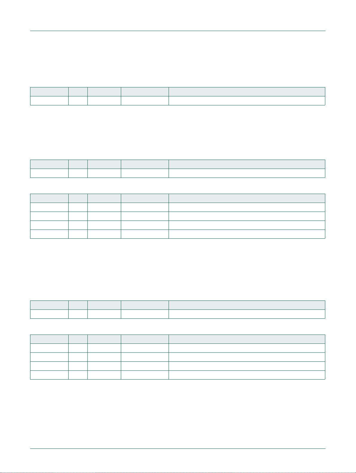
NXP Semiconductors
5.8.2 SH_CMD_RESET (0xA2) command
This command can be used to reset the LPC84x. This command has no response.
Table 55. Command packet
Field Offset Size (bytes) Value Description
command 0x0 0x1 0xA2 'Reset' command identifier
5.8.3 SH_CMD_BOOT (0xA3) command
This command can be used to boot the application currently programmed into flash, boot
address starting at 0x0. This command has a response only if the boot image does not
have a valid checksum.
Table 56. Command packet
Field Offset Size (bytes) Value Description
command 0x0 0x1 0xA3 'Boot' command identifier
UM11029
Chapter 5: LPC84x ISP and IAP
Table 57. Response packet
Field Offset Size (bytes) Value Description
sop 0x0 0x1 0x55 Start of packet identifier
command 0x1 0x1 0xA3 Processed command identifier
length 0x2 0x2 0x4 Length of the response packet on an error
errorCode 0x4 0x4 Error code Boot prevention due to invalid checksum.
5.8.4 SH_CMD_CHECK_IMAGE (0xA4) command
This command can be used to check the checksum value of the application currently
programmed into FLASH. The command verifies the checksum of the image. If the
checksum is valid, a response value of 0 is returned, otherwise, the checksum value is
returned.
Table 58. Command packet
Field Offset Size (bytes) Value Description
command 0x0 0x1 0xA4 'Check image' command identifier
Table 59. Response packet
Field Offset Size (bytes) Value Description
sop 0x0 0x1 0x55 Start of packet identifier
command 0x1 0x1 0xA4 Processed command identifier
length 0x2 0x2 0x04 Length of the response packet
checksum 0x4 0x4 CRC32 value 0x0 if match, otherwise the checksum value.
5.8.5 SH_CMD_PROBE (0xA5) command
The probe command is used to select either the I2C or SPI interface when in
auto-detection mode. This command is required when booting into the I2C/SPI ISP mode
from a reset condition. The probe command data is accepted on the supported I2C or SPI
UM11029 All information provided in this document is subject to legal disclaimers. © NXP B.V. 2017. All rights reserved.
User manual Rev. 1.0 — 16 June 2017 49 of 515
Page 50

NXP Semiconductors
ISP pins. Once the data is checked, the ISP1_IRQ line is driven LOW. The interface that
was used for the probe command becomes the active interface and the other interface is
disabled.
The probe command is optional when the I2C or SPI ISP mode is re-invoked from an
application using the ‘Re-invoke ISP’ IAP command. Only the interface selected with the
‘Re-invoke ISP’ IAP command will be active for the optional probe command.
The host system should repeatedly send the probe command to the LCP84x via one of
the supported interfaces until the LPC84x asserts the ISP1_IRQ pin LOW.
UM11029
Chapter 5: LPC84x ISP and IAP
Table 60. Command packet
Field Offset Size (bytes) Value Description
command 0x0 0x1 0xA5 ‘Probe’ command identifier
ifSel 0x1 0x1 Host interface type and port. Must match selected interface used to the
Reserved0 0x2 0x1 Set to 0x00
Reserved1 0x3 0x1 Set to 0x00
Reserved2 0x4 0x1 Set to 0x00
Reserved3 0x5 0x1 Set to 0x00
Reserved4 0x6 0x1 Set to 0x00
checksum 0x7 0x1 XOR of all the 7 bytes above.
Table 61. Response packet success
Field Offset Size (bytes) Value Description
sop 0x0 0x1 0x55 Start of packet identifier
command 0x1 0x1 0xA5 Processed command identifier
length 0x2 0x2 0x00 On Success, the XOR of the 7 bytes is zero and the interface number
LPC84x.
1 – I2C0 port
4 – SPI0 port
matches. Set to 0x00.
Table 62. Response packet error
Field Offset Size (bytes) Value Description
sop 0x0 0x1 0x55 Start of packet identifier
command 0x1 0x1 0xA5 Processed command identifier
length 0x2 0x2 0x04 On error this field is set to 4
errorCode 0x4 0x4 Error code Error code specified in error.h
5.8.6 SH_CMD_WRITE_BLOCK (0xA6) command
The write block command is used to write a block of data to flash. A block of data is 128
bytes.
UM11029 All information provided in this document is subject to legal disclaimers. © NXP B.V. 2017. All rights reserved.
User manual Rev. 1.0 — 16 June 2017 50 of 515
Page 51

NXP Semiconductors
UM11029
Chapter 5: LPC84x ISP and IAP
Table 63. Command packet
Field Offset Size (bytes) Value Description
command 0x0 0x1 0xA6 ‘Write block’ command identifier
crcCheck 0x1 0x1 0 – Do CRC check for this packet
1 - Ignore CRC field for this packet
blockNum 0x2 0x2 Flash block number in which the appended data to be programmed.
For example to program flash block 0x8000, this parameter should
be set to 256.
data 0x4 Block_size Data to be programmed in flash.
checksum Block_size + 4 0x4 CRC32 CRC32 of the packet excluding this field. Set this field to 0 if
crcCheck is set to 1.
Table 64. Response packet (success)
Field Offset Size (bytes) Value Description
sop 0x0 0x1 0x55 Start of packet identifier
command 0x1 0x1 0xA6 Processed command identifier
length 0x2 0x2 0x00 On success this field is set to 0.
Table 65. Response packet (error)
Field Offset Size (bytes) Value Description
sop 0x0 0x1 0x55 Start of packet identifier
command 0x1 0x1 0xA6 Processed command identifier
length 0x2 0x2 0x00 On error this field is set to 4
errorCode 0x4 0x4 Error code Error code specified in error.h
5.8.7 SH_CMD_READ_BLOCK (0xA7) command
The read block command is used to read a block of data from flash. A block of data is 128
bytes.
Table 66. Command packet
Field Offset Size (bytes) Value Description
command 0x0 0x1 0xA7 ‘Read block’ command identifier
reserved 0x1 0x1 Should be zero
blockNum 0x2 0x2 Flash block number to read. For example to read flash block
Table 67. Response packet (success)
Field Offset Size (bytes) Value Description
sop 0x0 0x1 0x55 Start of packet identifier
command 0x1 0x1 0xA7 Processed command identifier
length 0x2 0x2 Block_size + 4 Length of the response packet. Block_size + 4 =
data 0x4 Block_size Flash block content
checksum Block_size + 4 0x4 CRC32 CRC32 of the packet excluding this field
0x8000, this parameter should be set to 256.
success
UM11029 All information provided in this document is subject to legal disclaimers. © NXP B.V. 2017. All rights reserved.
User manual Rev. 1.0 — 16 June 2017 51 of 515
Page 52

NXP Semiconductors
UM11029
Chapter 5: LPC84x ISP and IAP
Table 68. Response packet (error)
Field Offset Size (bytes) Value Description
sop 0x0 0x1 0x55 Start of packet identifier
command 0x1 0x1 0xA7 Processed command identifier
length 0x2 0x2 0x4 Length of the response packet. 0x4 = failure
errorCode 0x4 0x4 Error code Error code specified in error.h
5.8.8 SH_CMD_SECTOR_ERASE (0xA8) command
The sector erase command is used to erase a sector in flash. A sector size is 1K bytes.
Table 69. Command packet
Field Offset Size (bytes) Value Description
command 0x0 0x1 0xA8 ‘Erase sector’ command identifier
reserved 0x1 0x1 Should be zero.
sectorNum 0x2 0x2 Flash sector number to be erased. For example to erase flash
Table 70. Response packet (success)
Field Offset Size (bytes) Value Description
sop 0x0 0x1 0x55 Start of packet identifier
command 0x1 0x1 0xA8 Processed command identifier
length 0x2 0x2 0x00 On success this field is set to 0.
sector at 0x2000, this parameter should be set to 8.
Table 71. Response packet (error)
Field Offset Size (bytes) Value Description
sop 0x0 0x1 0x55 Start of packet identifier
command 0x1 0x1 0xA8 Processed command identifier
length 0x2 0x2 0x4 On error this field is set to 4
errorCode 0x4 0x4 Error code Error code specified in error.h
5.8.9 SH_CMD_PAGE_ERASE (0xA9) command
The page erase command is used to erase a page in flash. A page size is 64 bytes.
Table 72. Command packet
Field Offset Size (bytes) Value Description
command 0x0 0x1 0xA9 ‘Page erase’ command identifier
reserved 0x1 0x1 Should be zero
pageNum 0x2 0x2 Flash page number to be erased. For example to erase flash
Table 73. Response packet (success)
Field Offset Size (bytes) Value Description
sop 0x0 0x1 0x55 Start of packet identifier
command 0x1 0x1 0xA9 Processed command identifier
length 0x2 0x2 0x00 Length of the response packet. 0x0 = success
page at 0x8000, this parameter should be set to 512.
UM11029 All information provided in this document is subject to legal disclaimers. © NXP B.V. 2017. All rights reserved.
User manual Rev. 1.0 — 16 June 2017 52 of 515
Page 53

NXP Semiconductors
UM11029
Chapter 5: LPC84x ISP and IAP
Table 74. Response packet (error)
Field Offset Size (bytes) Value Description
sop 0x0 0x1 0x55 Start of packet identifier
command 0x1 0x1 0xA9 Processed command identifier
length 0x2 0x2 0x4 Length of the response packet. 0x4 = failure
errorCode 0x4 0x4 Error code Error code specified in error.h parameters
5.8.10 SH_CMD_PAGE_WRITE (0xAA) command
The page write command is used to write a page in flash. A page size is 64 bytes.
Table 75. Command packet
Field Offset Size (bytes) Value Description
command 0x0 0x1 0xAA ‘Page write’ command identifier
crcCheck 0x1 0x1 0 – Do CRC check for this packet.
pageNum 0x2 0x2 Flash page number in which the appended data to be programmed.
data 0x4 Page_size Data to be programmed in flash.
checkSum Page_size+4 0x4 CRC32 CRC32 of the packet excluding this field. Set this field to 0 if
1 - Ignore CRC field for this packet.
For example to program flash page at 0x8000, this parameter should
be set to 512.
crcCheck is set to 1.
Table 76. Response packet (success)
Field Offset Size (bytes) Value Description
sop 0x0 0x1 0x55 Start of packet identifier
command 0x1 0x1 0xAA Processed command identifier
length 0x2 0x2 0x00 On success this field is set to 0
Table 77. Response packet (error)
Field Offset Size (bytes) Value Description
sop 0x0 0x1 0x55 Start of packet identifier
command 0x1 0x1 0xAA Processed command identifier
length 0x2 0x2 0x4 On error this field is set to 4
errorCode 0x4 0x4 Error code Error code specified in error.h parameters
5.8.1 1 SH_CMD_PAGE_READ (0xAB) command
The page read command is used to read a page in flash. A page size is 64 bytes.
Table 78. Command packet
Field Offset Size (bytes) Value Description
command 0x0 0x1 0xAB ‘Page read’ command identifier
crcCheck 0x1 0x1 0 – Do CRC check for this packet.
pageNum 0x2 0x2 Flash page number from which the data to be read.
1 - Ignore CRC field for this packet.
UM11029 All information provided in this document is subject to legal disclaimers. © NXP B.V. 2017. All rights reserved.
User manual Rev. 1.0 — 16 June 2017 53 of 515
Page 54
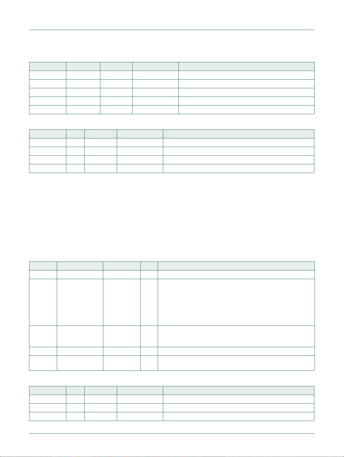
NXP Semiconductors
UM11029
Chapter 5: LPC84x ISP and IAP
Table 79. Response packet (success)
Field Offset Size (bytes) Value Description
sop 0x0 0x1 0x55 Start of packet identifier
command 0x1 0x1 0xAB Processed command identifier
length 0x2 0x2 Page_size+4 On success this field is set to Page_size+4
data 0x4 Page_size Flash page content.
checkSum Page_size+4 0x4 CRC32 CRC32 of the packet excluding this field
Table 80. Response packet (error)
Field Offset Size (bytes) Value Description
sop 0x0 0x1 0x55 Start of packet identifier
command 0x1 0x1 0xAB Processed command identifier
length 0x2 0x2 0x04 On error this field is set to 4
errorCode 0x4 0x4 Error code Error code specified in error.h parameters
5.8.12 SH_CMD_WRITE_SUBBLOCK (0xAC) command
The write sub-block command is used for queuing data for a full flash block write. It is
used when the host system cannot send the entire data block to the LPC84x in a single
I2C transfer using the ‘Write block’ command. When using this command, multiple
sub-blocks are sent to the LPC84x in sequential order for the block. The LPC84x collects
all the packets and performs the flash write once the last packet is received. If any other
commands are sent between ‘Write sub-block’ commands, the collected buffers are
discarded and the operations needs to restart. If a sub-block number crosses a block
boundary, the LPC84x automatically erases the sector prior to the write operation.
Table 81. Command packet
Field Offset Size (bytes) Value Description
command 0x0 0x1 0xAC ‘Write sub-block’ command identifier
subBlock 0x1 0x1 Bit 0: If set, CRC check is not done for this packet.
blockNum 0x2 0x2 Flash block number in which the appended data to be programed.
data 0x4 Sub-block size Data to be programmed in flash.
checkSum Sub-block size + 4 0x4 CRC32 of the packet excluding this field. Set this field to 0 if
Bits [5:1]: Specifies the sub-block number.
Bits [7:6]: Specifies the sub-block size.
00 – 32 bytes
01 – 64 bytes
10 – reserved
11 – reserved
For example to program sub-block at 0x8000 this parameter should
be set to 256.
crcCheck is set to 1.
Table 82. Response packet (success)
Field Offset Size (bytes) Value Description
sop 0x0 0x1 0x55 Start of packet identifier
command 0x1 0x1 0xAC Processed command identifier
length 0x2 0x2 0x00 On success this field is set to 0
UM11029 All information provided in this document is subject to legal disclaimers. © NXP B.V. 2017. All rights reserved.
User manual Rev. 1.0 — 16 June 2017 54 of 515
Page 55

NXP Semiconductors
UM11029
Chapter 5: LPC84x ISP and IAP
Table 83. Response packet (error)
Field Offset Size (bytes) Value Description
sop 0x0 0x1 0x55 Start of packet identifier
command 0x1 0x1 0xAC Processed command identifier
length 0x2 0x2 0x4 On error this field is set to 4
errorCode 0x4 0x4 Error code Error code specified in error.h parameters
5.8.13 SH_CMD_ READ_SUBBLOCK (0xAD) command
The read sub-block command is used for reading partial data from a full flash block write.
It is used when the host system cannot receive the entire data block to the LPC84x in a
single I2C transfer using the ‘Read block’ command.
Table 84. Command packet
Field Offset Size (bytes) Value Description
command 0x0 0x1 0xAD ‘Read subblock’ command identifier
subBlock 0x1 0x1 Bit 0: If set, CRC check is not done for this packet.
blockNum 0x2 0x2 Flash block number to read. For example to read sub-block at
Bits [5:1]: Specifies the sub-block number
Bits [7:6]: Specifies the sub-block size
00 – 32 bytes
01 – 64 bytes
10 – reserved
11 – reserved
0x8000 this parameter should be set to 256.
Table 85. Response packet (success)
Field Offset Size (bytes) Value Description
sop 0x0 0x1 0x55 Start of packet identifier
command 0x1 0x1 0xAD Processed command identifier
length 0x2 0x2 Sub-block size + 4 On success this field is set to (Sub-block size + 4)
data 0x4 0x2 Sub-block size Flash data
checksum Sub-block size + 4 0x4 CRC32 of the packet excluding this field
Table 86. Response packet (error)
Field Offset Size (bytes) Value Description
sop 0x0 0x1 0x55 Start of packet identifier
command 0x1 0x1 0xAD Processed command identifier
length 0x2 0x2 0x4 On error this field is set to 4
errorCode 0x4 0x4 Error code Error code specified in error.h parameters
5.8.14 SH_CMD_BULK_ERASE (0xAE) command
The bulk erase command is used to erase more than one sector (from a start sector to an
end sector).
UM11029 All information provided in this document is subject to legal disclaimers. © NXP B.V. 2017. All rights reserved.
User manual Rev. 1.0 — 16 June 2017 55 of 515
Page 56

NXP Semiconductors
UM11029
Chapter 5: LPC84x ISP and IAP
Table 87. Command packet
Field Offset Size (bytes) Value Description
command 0x0 0x1 0xAE ‘Bulk erase’ command identifier
reserved 0x1 0x1 - -
startSec 0x2 0x1 - Starting sector number to erase
endsec 0x3 0x1 - End sector number to erase
Table 88. Response packet (success)
Field Offset Size (bytes) Value Description
sop 0x0 0x1 0x55 Start of packet identifier
command 0x1 0x1 0xAE Processed command identifier
length 0x2 0x2 0x00 On success this field is set to 0
Table 89. Response packet (error)
Field Offset Size (bytes) Value Description
sop 0x0 0x1 0x55 Start of packet identifier
command 0x1 0x1 0xAE Processed command identifier
length 0x2 0x2 0x4 On error this field is set to 4
errorCode 0x4 0x4 Error code Error code specified in error.h parameters
5.8.15 SH_CMD_WRITE_RAM (0xB0) command
This command is used to write a block of data to the RAM. The RAM between 0x1000000
and 0x10007FF is reserved by the I2C/SPI ISP.
Table 90. Command packet
Field Offset Size (bytes) Value Description
command 0x0 0x1 0xB0 ‘Write RAM’ command identifier
crcCheck 0x1 0x1 0 – CRC check not enabled
size 0x2 0x2 length Number of bytes to be written to the RAM. The size must be word
addr 0x4 0x4 Beginning address to be written in RAM, must be >= 0x10000800 if
checksum 0x8 0x4 CRC32 CRC32 of the packet excluding this field. Set this field to 0 if crcCheck
data 0xC length Data string to be written to the RAM
Table 91. Response packet (success)
Field Offset Size (bytes) Value Description
sop 0x0 0x1 0x55 Start of packet identifier
command 0x1 0x1 0xB0 Processed command identifier
length 0x2 0x2 0x0 Length of the response packet. 0x0 = success
1 – CRC check enabled
aligned.
CRP1 is enabled.
is set to 1.
UM11029 All information provided in this document is subject to legal disclaimers. © NXP B.V. 2017. All rights reserved.
User manual Rev. 1.0 — 16 June 2017 56 of 515
Page 57

NXP Semiconductors
UM11029
Chapter 5: LPC84x ISP and IAP
Table 92. Response packet (error)
Field Offset Size (bytes) Value Description
sop 0x0 0x1 0x55 Start of packet identifier
command 0x1 0x1 0xB0 Processed command identifier
length 0x2 0x2 0x4 Length of the response packet. 0x4 = failure
errorCode 0x4 0x4 Error code Error code specified in error.h parameters
5.8.16 SH_CMD_GOTO (0xB1) command
This command is used to jump to user code based on the address given in the command
packet.
Table 93. Command packet
Field Offset Size (bytes) Value Description
command 0x0 0x1 0xB1 ‘GoTo’ command identifier
address 0x4 0x4 Code address to jump to user code
Table 94. Response packet (error)
Field Offset Size (bytes) Value Description
sop 0x0 0x1 0x55 Start of packet identifier
command 0x1 0x1 0xB1 Processed command identifier
length 0x2 0x2 0x4 Length of the response packet. 0x4 = failure
errorCode 0x4 0x4 Error code Error code specified in error.h
If there is an error in the command, there is a response packet as shown in Table 94.
5.8.17 SH_CMD_FAIM_READ (0xBE) command
This command is used to read one page from the FAIM memory. One page of FAIM is 4
bytes.
Table 95. Command packet
Field Offset Size (bytes) Value Description
command 0x0 0x1 0xBE ‘Read block’ command identifier
reserved 0x1 0x1 zero
PageNum 0x2 0x2 FAIM page number to read
Table 96. Response packet (success)
Field Offset Size (bytes) Value Description
sop 0x0 0x1 0x55 Start of packet identifier
command 0x1 0x1 0xBE Processed command identifier
length 0x2 0x2 0x08 One page is 4 bytes. Length of the response packet. 0x8 =
data 0x4 0x4 FAIM page content
checksum 0x8 0x4 CRC32 CRC32 of the packet excluding this field.
success
UM11029 All information provided in this document is subject to legal disclaimers. © NXP B.V. 2017. All rights reserved.
User manual Rev. 1.0 — 16 June 2017 57 of 515
Page 58

NXP Semiconductors
UM11029
Chapter 5: LPC84x ISP and IAP
Table 97. Response packet (error)
Field Offset Size (bytes) Value Description
sop 0x0 0x1 0x55 Start of packet identifier
command 0x1 0x1 0xBE Processed command identifier
length 0x2 0x2 0x4 Length of the response packet. 0x4 = failure
errorCode 0x4 0x4 Error code Error code specified in error.h
5.8.18 SH_CMD_FAIM_WRITE (0xBF) command
This command is used to write one page to the FAIM memory. One page of FAIM is 4
bytes.
Table 98. Command packet
Field Offset Size (bytes) Value Description
command 0x0 0x1 0xBF ‘FAIM write’ command identifier
crcCheck 0x1 0x1 00 – Do CRC check for this packet
PageNum 0x2 0x2 Page number to program data
data 0x4 0x4 Data to be programmed in FAIM
checksum 0x8 0x4 CRC32 CRC32 of the packet excluding this field. Set this field to 0 if crcCheck
01 – Ignore CRC field for this packet
is set to 1.
Table 99. Response packet (success)
Field Offset Size (bytes) Value Description
sop 0x0 0x1 0x55 Start of packet identifier
command 0x1 0x1 0xBF Processed command identifier
length 0x2 0x2 0x00 On success this field is set to 0
Table 100. Response packet (error)
Field Offset Size (bytes) Value Description
sop 0x0 0x1 0x55 Start of packet identifier
command 0x1 0x1 0xBF Processed command identifier
length 0x2 0x2 0x4 Length of the response packet. 0x4 = failure
errorCode 0x4 0x4 Error code Error code specified in error.h
5.8.19 I2C/SPI ISP Error codes
See Tab le 3 6 “ ISP/IAP Error codes”.
5.8.20 I2C/SPI ISP mode protocol software support
This section includes predefined command definitions and software structures used for
communication for the I2C/SPI ISP protocol. These may be used with a host application
that talks to the I2C/SPI ISP interface via the supported I2C or SPI slave interfaces.
/* I2C/SPI IMSP mode protocol commands */
#define SH_CMD_GET_VERSION 0xA1
#define SH_CMD_RESET 0xA2
#define SH_CMD_BOOT 0xA3
UM11029 All information provided in this document is subject to legal disclaimers. © NXP B.V. 2017. All rights reserved.
User manual Rev. 1.0 — 16 June 2017 58 of 515
Page 59

NXP Semiconductors
#define SH_CMD_CHECK_IMAGE 0xA4
#define SH_CMD_PROBE 0xA5
#define SH_CMD_WRITE_BLOCK 0xA6
#define SH_CMD_READ_BLOCK 0xA7
#define SH_CMD_SECTOR_ERASE 0xA8
#define SH_CMD_PAGE_ERASE 0xA9
#define SH_CMD_PAGE_WRITE 0xAA
#define SH_CMD_PAGE_READ 0xAB
#define SH_CMD_WRITE_SUBBLOCK 0xAC
#define SH_CMD_READ_SUBBLOCK 0xAD
#define SH_CMD_BULK_ERASE 0xAE
#define SH_CMD_WRITE_RAM 0xB0
#define SH_CMD_GOTO 0xB1
#define SH_CMD_FAIM_READ 0xBE
#define SH_CMD_FAIM_WRITE 0xBF
/** Structure describing response packet format. */
typedef struct {
} CmdResponse_t;
UM11029
Chapter 5: LPC84x ISP and IAP
uint8_t sop; /*!< Start of packet = 0x55 for bootloader */
uint8_t cmd; /*!< Response to the Command ID. */
uint16_t length; /*!< Response data length not including this header. */
/** Structure describing Read/Write block command packet format. */
typedef struct {
uint8_t cmd; /*!< Command ID */
uint8_t crc_check; /*!< specifies if we need to do CRC check before processing */
uint16_t block_nr; /*!< Block number.*/
uint32_t data[SL_FLASH_BLOCK_SZ/4]; /*!< Data */
uint32_t crc32; /*!< CRC32 of command header and data */
} CmdRWBlockParam_t;
. . .....
/** Structure describing Read/Write page command packet format. */
typedef struct {
uint8_t cmd; /*!< Command ID */
uint8_t crc_check; /*!< specifies if we need to do CRC check before processing */
uint16_t page_nr; /*!< page number.*/
uint32_t data[SL_FLASH_PAGE_SZ/4]; /*!< Data */
uint32_t crc32; /*!< CRC32 of command header and data */
} CmdRWPageParam_t;
/** Structure describing Read sub-block command packet format. */
typedef struct {
uint8_t cmd; /*!< Command ID */
uint8_t sub_block_nr; /*!< specifies the sub-block number. Bits below:
0 - Skip crc;
5-1: sub block nr;
7-6: sub-block size. 0 - 32, 1 - 64, 2 - 128, 3 - 256 */
uint16_t block_nr; /*!< block number.*/
uint32_t data[SL_FLASH_BLOCK_SZ/4]; /*!< Data */
} CmdReadSubBlockParam_t;
/** Structure describing Sector erase command packet format. */
UM11029 All information provided in this document is subject to legal disclaimers. © NXP B.V. 2017. All rights reserved.
User manual Rev. 1.0 — 16 June 2017 59 of 515
Page 60

NXP Semiconductors
typedef struct {
} CmdEraseSectorParam_t;
/** Structure describing Bulk erase command packet format. */
typedef struct {
} CmdBulkEraseParam_t;
/** Structure describing response packet with data. */
typedef struct {
} CmdDataResp_t;
typedef enum
{
UM11029
Chapter 5: LPC84x ISP and IAP
uint8_t cmd; /*!< Command ID */
uint8_t reserved; /*!< Should be zero. */
uint16_t sec_nr; /*!< Sector number.*/
uint8_t cmd; /*!< Command ID */
uint8_t reserved; /*!< Should be zero. */
uint8_t start_sec; /*!< Start Sector number.*/
uint8_t end_sec; /*!< End Sector number.*/
CmdResponse_t hdr; /*!< Response header. */
uint32_t data[SL_FLASH_BLOCK_SZ/4]; /*!< Data */
uint32_t crc32; /*!< CRC32 of response packet. */
UM11029 All information provided in this document is subject to legal disclaimers. © NXP B.V. 2017. All rights reserved.
User manual Rev. 1.0 — 16 June 2017 60 of 515
Page 61

UM11029
Chapter 6: LPC84x Flash signature generator
Rev. 1.0 — 16 June 2017 User manual
6.1 How to read this chapter
The flash signature generator is identical on all LPC84x parts.
6.2 Features
• Controls flash access time.
• Provides registers for flash signature generation.
6.3 General description
The flash signature generator is accessible for programming flash wait states and for
generating the flash signature.
6.4 Register description
Table 101. Register overview: FMC (base address 0x4004 0000)
Name Access Address offset Description Reset
FLASHCFG R/W 0x010 Flash configuration register - Section 6.4.1
FMSSTART R/W 0x020 Signature start address register 0 Section 6.4.2
FMSSTOP R/W 0x024 Signature stop-address register 0 Section 6.4.3
FMSW0 R 0x02C Signature word - Section 6.4.4
FMSTAT R 0xFE0 Signature generation status register 0 Section 6.4.5
FMSTATCLR W 0xFE8 Signature generation status clear register. - Section 6.4.6
6.4.1 Flash configuration register
Reference
value
Access time to the flash memory can be configured independently of the system
frequency by writing to the FLASHCFG register.
Table 102. Flash configuration register (FLASHCFG, address 0x4004 0010) bit description
Bit Symbol Value Description Reset
value
1:0 FLASHTIM Flash memory access time. FLASHTIM +1 is equal to the
number of system clocks used for flash access.
0x0 1 system clock flash access time.
0x1 2 system clocks flash access time.
0x2 3 system clocks flash access time.
0x3 Reserved.
31:2 - - Reserved. User software must not change the value of
these bits. Bits 31:2 must be written back exactly as
read.
0x2
-
UM11029 All information provided in this document is subject to legal disclaimers. © NXP Semiconductors N.V. 2017. All rights reserved.
User manual Rev. 1.0 — 16 June 2017 61 of 515
Page 62

NXP Semiconductors
6.4.2 Flash signature start address register
T able 103. Flash Module Signature Start register (FMSSTART, 0x4004 0020) bit description
Bit Symbol Description Reset
16:0 START Signature generation start address (corresponds to AHB byte
31:17 - Reserved, user software should not write ones to reserved bits.
6.4.3 Flash signature stop address register
Table 104. Flash Module Signature Stop register (FMSSTOP, 0x4004 0024) bit description
Bit Symbol Value Description Reset
16:0 STOPA Stop address for signature generation (the word
30:17 - Reserved, user software should not write ones to
31 STRTBIST When this bit is written to 1, signature generation starts.
UM11029
Chapter 6: LPC84x Flash signature generator
value
0
address bits[18:2]).
NA
The value read from a reserved bit is not defined.
value
0
specified by STOPA is included in the address range).
The address is in units of memory words, not bytes.
0
reserved bits. The value read from a reserved bit is not
defined.
0
At the end of signature generation, this bit is
automatically cleared.
6.4.4 Flash signature generation result register
The signature generation result register returns the flash signature produced by the
embedded signature generator.
The generated flash signature can be used to verify the flash memory contents. The
generated signature can be compared with an expected signature and thus makes saves
time and code space. The method for generating the signature is described in
Section 6.5.1
Table 105. FMSW0 register bit description (FMSW0, address: 0x4004 002C)
Bit Symbol Description Reset value
31:0 SIG 32-bit signature. -
.
6.4.5 Flash module signature status register
The read-only FMSTAT register provides a means of determining when signature
generation has completed. Completion of signature generation can be checked by polling
the SIG_DONE bit in FMSTAT. SIG_DONE should be cleared via the FMSTATCLR
register before starting a signature generation operation, otherwise the status might
indicate completion of a previous operation.
UM11029 All information provided in this document is subject to legal disclaimers. © NXP Semiconductors N.V. 2017. All rights reserved.
User manual Rev. 1.0 — 16 June 2017 62 of 515
Page 63

NXP Semiconductors
UM11029
Chapter 6: LPC84x Flash signature generator
Table 106. Flash module signature status register (FMSTAT, offset 0x0FE0) bit description
Bit Symbol Description Reset value
1:0 - Reserved. Read value is undefined, only zero should be written. NA
2 SIG_DONE When 1, a previously started signature generation has completed. See FMSTATCLR
0
register description for clearing this flag.
31:2 - Reserved. Read value is undefined, only zero should be written. NA
6.4.6 Flash module signature status clear register
The FMSTATCLR register is used to clear the signature generation completion flag.
Table 107. Flash module signature status clear register (FMSTATCLR, offset 0x0FE8) bit description
Bit Symbol Description Reset value
1:0 - Reserved. Read value is undefined, only zero should be written. NA
2 SIG_DONE_CLR Writing a 1 to this bits clears the signature generation completion flag
31:2 - Reserved. Read value is undefined, only zero should be written. NA
0
(SIG_DONE) in the FMSTAT register.
UM11029 All information provided in this document is subject to legal disclaimers. © NXP Semiconductors N.V. 2017. All rights reserved.
User manual Rev. 1.0 — 16 June 2017 63 of 515
Page 64

NXP Semiconductors
6.5 Functional description
6.5.1 Flash signature generation
The flash module contains a built-in signature generator. This generator can produce a
32-bit signature from a range of flash memory. A typical usage is to verify the flashed
contents against a calculated signature (e.g. during programming).
The address range for generating a signature must be aligned on flash-word boundaries,
that is, 32-bit boundaries. Once started, signature generation completes independently.
While signature generation is in progress, the flash memory cannot be accessed for other
purposes, and an attempted read will cause a wait state to be asserted until signature
generation is complete. Code outside of the flash (e.g. internal RAM) can be executed
during signature generation. This can include interrupt services, if the interrupt vector
table is re-mapped to memory other than the flash memory. The code that initiates
signature generation should also be placed outside of the flash memory.
6.5.1.1 Signature generation address and control registers
These registers control automatic signature generation. A signature can be generated for
any part of the flash memory contents. The address range to be used for generation is
defined by writing the start address to the signature start address register (FMSSTART)
and the stop address to the signature stop address register (FMSSTOP. The start and
stop addresses must be aligned to 32-bit boundaries.
UM11029
Chapter 6: LPC84x Flash signature generator
Signature generation is started by setting the STRTBIST bit in the FMSSTOP register.
Setting the STRTBIST bit is typically combined with the signature stop address in a single
write.
Table 103
registers respectively.
and Table 104 show the bit assignments in the FMSSTART and FMSSTOP
6.5.1.2 Signature generation
A signature can be generated for any part of the flash contents. The address range to be
used for signature generation is defined by writing the start address to the FMSSTART
register, and the stop address to the FMSSTOP register.
The signature generation is started by writing a 1 to the SIG_START bit in the FMSSTOP
register. Starting the signature generation is typically combined with defining the stop
address, which is done in the STOP bits of the same register.
The time that the signature generation takes is proportional to the address range for which
the signature is generated. Reading of the flash memory for signature generation uses a
self-timed read mechanism and does not depend on any configurable timing settings for
the flash. A safe estimation for the duration of the signature generation is:
Duration = int((60 / tcy) + 3) x (FMSSTOP - FMSSTART + 1)
When signature generation is triggered via software, the duration is in AHB clock cycles,
and tcy is the time in ns for one AHB clock. The SIG_DONE bit in FMSTAT can be polled
by software to determine when signature generation is complete.
UM11029 All information provided in this document is subject to legal disclaimers. © NXP Semiconductors N.V. 2017. All rights reserved.
User manual Rev. 1.0 — 16 June 2017 64 of 515
Page 65

NXP Semiconductors
After signature generation, a 32-bit signature can be read from the FMSW0 register. The
32-bit signature reflects the corrected data read from the flash and the flash parity bits and
check bit values.
6.5.1.3 Content verification
The signature as it is read from the FMSW0 register must be equal to the reference
signature. The following pseudo-code shows the algorithm to derive the reference
signature:
sign = 0
FOR address = FMSSTART.START to FMSSTOP.STOPA
{
{
}
signature32 = sign
UM11029
Chapter 6: LPC84x Flash signature generator
FOR i = 0 TO 30
nextSign[i] = f_Q[address][i] XOR sign[i + 1]
}
nextSign[31] = f_Q[address][31] XOR sign[0] XOR sign[10] XOR sign[30] XOR
sign[31]
sign = nextSign
UM11029 All information provided in this document is subject to legal disclaimers. © NXP Semiconductors N.V. 2017. All rights reserved.
User manual Rev. 1.0 — 16 June 2017 65 of 515
Page 66

UM11029
Chapter 7: LPC84x Nested Vectored Interrupt Controller (NVIC)
Rev. 1.0 — 16 June 2017 User manual
7.1 How to read this chapter
The NVIC is identical on all LPC84x parts.
7.2 Features
• Nested Vectored Interrupt Controller that is an integral part of the ARM Cortex-M0+.
• Tightly coupled interrupt controller provides low interrupt latency.
• Controls system exceptions and peripheral interrupts.
• The NVIC supports 32 vectored interrupts.
• Four programmable interrupt priority levels with hardware priority level masking.
• Software interrupt generation using the ARM exceptions SVCall and PendSV (see
Ref. 3
).
• Support for NMI.
• ARM Cortex M0+ Vector table offset register VTOR implemented.
7.3 General description
The Nested Vectored Interrupt Controller (NVIC) is an integral part of the Cortex-M0+. The
tight coupling to the CPU allows for low interrupt latency and efficient processing of late
arriving interrupts.
7.3.1 Interrupt sources
Table 108 lists the interrupt sources for each peripheral function. Each peripheral device
may have one or more interrupt lines to the Vectored Interrupt Controller. Each line may
represent more than one interrupt source. Interrupts with the same priority level are
serviced in the order of their interrupt number.
See Ref. 3
Table 108. Connection of interrupt sources to the NVIC
Interrupt
number
0 SPI0_IRQ SPI0 interrupt See Table 340 “
1 SPI1_IRQ SPI1 interrupt Same as SPI0_IRQ
2 DAC0_IRQ DAC0 interrupt -
Name Description Flags
for a detailed description of the NVIC and the NVIC register description.
SPI Interrupt Enable read and Set
register (INTENSET, addresses 0x4005 800C (SPI0),
0x4005 C00C (SPI1)) bit description”.
UM11029 All information provided in this document is subject to legal disclaimers. © NXP Semiconductors N.V. 2017. All rights reserved.
User manual Rev. 1.0 — 16 June 2017 66 of 515
Page 67

NXP Semiconductors
UM11029
Chapter 7: LPC84x Nested Vectored Interrupt Controller (NVIC)
Table 108. Connection of interrupt sources to the NVIC
Interrupt
number
3 UART0_IRQ USART0 interrupt See Table 326 “USART Interrupt Enable read and set
4 UART1_IRQ USART1 interrupt Same as UART0_IRQ
5 UART2_IRQ USART2 interrupt Same as UART0_IRQ
6 - Reserved -
7 I2C1_IRQ I2C1 interrupt See Table 356 “
8 I2C0_IRQ I2C0 interrupt See Table 356 “
9 SCT_IRQ State configurable timer
10 MRT_IRQ Multi-rate timer interrupt Global MRT interrupt.
11 CMP_IRQ Analog comparator interrupt COMPEDGE - rising, falling, or both edges can set the
12 WDT_IRQ Windowed watchdog timer
13 BOD_IRQ BOD interrupts BODINTVAL - BOD interrupt level
14 FLASH_IRQ flash interrupt -
15 WKT_IRQ Self-wake-up timer interrupt ALARMFLAG
16 ADC_SEQA_IRQ ADC sequence A
17 ADC_SEQB_IRQ ADC sequence B
18 ADC_THCMP_IRQ ADC threshold compare -
19 ADC_OVR_IRQ ADC overrun -
20 DMA_IRQ DMA interrupt -
21 I2C2_IRQ I2C2 interrupt See Table 356 “
22 I2C3_IRQ I2C3 interrupt See Table 356 “
23 CT32B0_IRQ Timer interrupt -
Name Description Flags
register (INTENSET, address 0x4006 400C (USART0),
0x4006 800C (USART1), 0x4006C00C (USART2),
0x4007 000C (USART3), 0x4007 400C (USART4)) bit
description”
Interrupt Enable Clear register
(INTENCLR, address 0x4005 000C (I2C0), 0x4005 400C
(I2C1), 0x4003 000C (I2C2), 0x4003 400C (I2C3)) bit
description”.
Interrupt Enable Clear register
(INTENCLR, address 0x4005 000C (I2C0), 0x4005 400C
(I2C1), 0x4003 000C (I2C2), 0x4003 400C (I2C3)) bit
description”.
EVFLAG SCT event
interrupt
GFLAG0
GFLAG1
GFLAG2
GFLAG3
bit.
WARNINT - watchdog warning interrupt
interrupt
-
completion
-
completion
Interrupt Enable Clear register
(INTENCLR, address 0x4005 000C (I2C0), 0x4005 400C
(I2C1), 0x4003 000C (I2C2), 0x4003 400C (I2C3)) bit
description”.
Interrupt Enable Clear register
(INTENCLR, address 0x4005 000C (I2C0), 0x4005 400C
(I2C1), 0x4003 000C (I2C2), 0x4003 400C (I2C3)) bit
description”.
UM11029 All information provided in this document is subject to legal disclaimers. © NXP Semiconductors N.V. 2017. All rights reserved.
User manual Rev. 1.0 — 16 June 2017 67 of 515
Page 68

NXP Semiconductors
Chapter 7: LPC84x Nested Vectored Interrupt Controller (NVIC)
Table 108. Connection of interrupt sources to the NVIC
Interrupt
number
24 PININT0_IRQ Pin interrupt 0 or pattern
25 PININT1_IRQ Pin interrupt 1 or pattern
26 PININT2_IRQ Pin interrupt 2 or pattern
27 PININT3_IRQ Pin interrupt 3 or pattern
28 PININT4_IRQ Pin interrupt 4 or pattern
29 PININT5_IRQ or
30 PININT6_IRQ r
31 PININT7_IRQ or
Name Description Flags
match engine slice 0
interrupt
match engine slice 1
interrupt
match engine slice 2
interrupt
match engine slice 3
interrupt
match engine slice 4
interrupt
Pin interrupt 5 or pattern
DAC1_IRQ
USART3_IRQ
USART4_IRQ
match engine slice 5
interrupt or DAC1 interrupt
Pin interrupt 6 or pattern
match engine slice 6
interrupt or USART3
interrupt
Pin interrupt 7 or pattern
match engine slice 7
interrupt or USART4
interrupt
UM11029
PSTAT - pin interrupt status
PSTAT - pin interrupt status
PSTAT - pin interrupt status
PSTAT - pin interrupt status
PSTAT - pin interrupt status
PSTAT - pin interrupt status
PSTAT - pin interrupt status
PSTAT - pin interrupt status
7.3.2 Non-Maskable Interrupt (NMI)
The part supports the NMI, which can be triggered by an peripheral interrupt or triggered
by software. The NMI has the highest priority exception other than the reset.
You can set up any peripheral interrupt listed in Table 108
register in the SYSCON block (Table 166
). To avoid using the same peripheral interrupt as
as NMI using the NMISRC
NMI exception and normal interrupt, disable the interrupt in the NVIC when you configure
it as NMI.
7.3.3 Vector table offset
The vector table contains the reset value of the stack pointer and the start addresses, also
called exception vectors, for all exception handlers. On system reset, the vector table is
located at address 0x0000 0000. Software can write to the VTOR register in the NVIC to
relocate the vector table start address to a different memory location. For a description of
the VTOR register, see the ARM Cortex-M0+ documentation (Ref. 3
UM11029 All information provided in this document is subject to legal disclaimers. © NXP Semiconductors N.V. 2017. All rights reserved.
User manual Rev. 1.0 — 16 June 2017 68 of 515
).
Page 69

NXP Semiconductors
UM11029
Chapter 7: LPC84x Nested Vectored Interrupt Controller (NVIC)
7.4 Register description
The NVIC registers are located on the ARM private peripheral bus.
offset
Description Reset
value
0 Ta b le 11 0
interrupts and reading back the interrupt enables for specific
peripheral functions.
0 Ta b le 11 1
interrupts and reading back the interrupt enables for specific
peripheral functions.
0 Ta b le 11 2
interrupt state to pending and reading back the interrupt pending
state for specific peripheral functions.
0 Ta b le 11 3
interrupt state to not pending and reading back the interrupt pending
state for specific peripheral functions.
0 Ta b le 11 4
current interrupt active state for specific peripheral functions.
0 Ta b le 11 5
to each interrupt. This register contains the 2-bit priority fields for
interrupts 0 to 3.
0 Ta b le 11 6
to each interrupt. This register contains the 2-bit priority fields for
interrupts 4 to 7.
0 Ta b le 11 7
to each interrupt. This register contains the 2-bit priority fields for
interrupts 8 to 11.
0 Ta b le 11 8
to each interrupt. This register contains the 2-bit priority fields for
interrupts 12 to 15.
0 Ta b le 11 9
to each interrupt. This register contains the 2-bit priority fields for
interrupts 16 to 19.
0 Ta b le 1 20
to each interrupt. This register contains the 2-bit priority fields for
interrupts 20 to 23.
0 Ta b le 1 21
to each interrupt. This register contains the 2-bit priority fields for
interrupts 24 to 27.
0 Ta b le 1 22
to each interrupt. This register contains the 2-bit priority fields for
interrupts 28 to 31.
Table 109. Register overview: NVIC (base address 0xE000 E000)
Name Access Address
ISER0 RW 0x100 Interrupt Set Enable Register 0. This register allows enabling
- - 0x104 Reserved. - -
ICER0 RW 0x180 Interrupt Clear Enable Register 0. This register allows disabling
- - 0x184 Reserved. 0 -
ISPR0 RW 0x200 Interrupt Set Pending Register 0. This register allows changing the
- - 0x204 Reserved. 0 -
ICPR0 RW 0x280 Interrupt Clear Pending Register 0. This register allows changing the
- - 0x284 Reserved. 0 -
IABR0 RO 0x300 Interrupt Active Bit Register 0. This register allows reading the
- - 0x304 Reserved. 0 -
IPR0 RW 0x400 Interrupt Priority Registers 0. This register allows assigning a priority
IPR1 RW 0x404 Interrupt Priority Registers 1 This register allows assigning a priority
IPR2 RW 0x408 Interrupt Priority Registers 2. This register allows assigning a priority
IPR3 RW 0x40C Interrupt Priority Registers 3. This register allows assigning a priority
IPR4 RW 0x410 Interrupt Priority Registers 4. This register allows assigning a priority
IPR5 RW 0x414 Interrupt Priority Registers 5. This register allows assigning a priority
IPR6 RW 0x418 Interrupt Priority Registers 6. This register allows assigning a priority
IPR7 RW 0x41C Interrupt Priority Registers 7. This register allows assigning a priority
Reference
UM11029 All information provided in this document is subject to legal disclaimers. © NXP Semiconductors N.V. 2017. All rights reserved.
User manual Rev. 1.0 — 16 June 2017 69 of 515
Page 70

NXP Semiconductors
UM11029
Chapter 7: LPC84x Nested Vectored Interrupt Controller (NVIC)
7.4.1 Interrupt Set Enable Register 0 register
The ISER0 register allows to enable peripheral interrupts or to read the enabled state of
those interrupts. Disable interrupts through the ICER0 (Section 7.4.2
The bit description is as follows for all bits in this register:
Write — Writing 0 has no effect, writing 1 enables the interrupt.
Read — 0 indicates that the interrupt is disabled, 1 indicates that the interrupt is enabled.
Table 110. Interrupt Set Enable Register 0 register (ISER0, address 0xE000 E100) bit description
Bit Symbol Description Reset value
0 ISE_SPI0 Interrupt enable. 0
1 ISE_SPI1 Interrupt enable. 0
2 ISE_DAC0 Interrupt enable. 0
3 ISE_UART0 Interrupt enable. 0
4 ISE_UART1 Interrupt enable. 0
5 ISE_UART2 Interrupt enable. 0
6 - Reserved 0
7 ISE_I2C1 Interrupt enable. 0
8 ISE_I2C0 Interrupt enable. 0
9 ISE_SCT Interrupt enable. 0
10 ISE_MRT Interrupt enable. 0
11 ISE_CMP Interrupt enable for comparator. 0
12 ISE_WDT Interrupt enable. 0
13 ISE_BOD Interrupt enable. 0
14 ISE_FLASH Interrupt enable. 0
15 ISE_WKT Interrupt enable. 0
16 ISE_ADC_SEQA Interrupt enable. 0
17 ISE_ADC_SEQB Interrupt enable. 0
18 ISE_ADC_THCMP Interrupt enable. 0
19 ISE_ADC_OVR Interrupt enable. 0
20 ISE_SDMA Interrupt enable. 0
21 ISE_I2C2 Interrupt enable. 0
22 ISE_I2C3 Interrupt enable. 0
23 ISE_CT32b0 Interrupt enable. 0
24 ISE_PININT0 Interrupt enable. 0
25 ISE_PININT1 Interrupt enable. 0
26 ISE_PININT2 Interrupt enable. 0
27 ISE_PININT3 Interrupt enable. 0
28 ISE_PININT4 Interrupt enable. 0
29 ISE_PININT5 or ISE_DAC1 Interrupt enable for both pinint5 and DAC1. 0
30 ISE_PININT6 or ISE_USART3 Interrupt enable for both pinint6 and USART3. 0
31 ISE_PININT7or ISE_USART4 Interrupt enable for both pinint7 and USART4. 0
).
UM11029 All information provided in this document is subject to legal disclaimers. © NXP Semiconductors N.V. 2017. All rights reserved.
User manual Rev. 1.0 — 16 June 2017 70 of 515
Page 71

NXP Semiconductors
Chapter 7: LPC84x Nested Vectored Interrupt Controller (NVIC)
7.4.2 Interrupt clear enable register 0
The ICER0 register allows disabling the peripheral interrupts, or for reading the enabled
state of those interrupts. Enable interrupts through the ISER0 registers (Section 7.4.1
The bit description is as follows for all bits in this register:
Write — Writing 0 has no effect, writing 1 disables the interrupt.
Read — 0 indicates that the interrupt is disabled, 1 indicates that the interrupt is enabled.
Table 111. Interrupt clear enable register 0 (ICER0, address 0xE000 E180)
Bit Symbol Description Reset value
0 ICE_SPI0 Interrupt disable. 0
1 ICE_SPI1 Interrupt disable. 0
2 ICE_DAC0 Interrupt disable. 0
3 ICE_UART0 Interrupt disable. 0
4 ICE_UART1 Interrupt disable. 0
5 ICE_UART2 Interrupt disable. 0
6 - Reserved 0
7 ICE_I2C1 Interrupt disable. 0
8 ICE_I2C0 Interrupt disable. 0
9 ICE_SCT Interrupt disable. 0
10 ICE_MRT Interrupt disable. 0
11 ICE_CMP Interrupt disable for comparator. 0
12 ICE_WDT Interrupt disable. 0
13 ICE_BOD Interrupt disable. 0
14 ICE_FLASH Interrupt disable. 0
15 ICE_WKT Interrupt disable. 0
16 ICE_ADC_SEQA Interrupt disable. 0
17 ICE_ADC_SEQB Interrupt disable. 0
18 ICE_ADC_THCMP Interrupt disable. 0
19 ICE_ADC_OVR Interrupt disable. 0
20 ICE_SDMA Interrupt disable. 0
21 ICE_I2C2 Interrupt disable. 0
22 ICE_I2C3 Interrupt disable. 0
23 ICE_CT32B0 Interrupt disable. 0
24 ICE_PININT0 Interrupt disable. 0
25 ICE_PININT1 Interrupt disable. 0
26 ICE_PININT2 Interrupt disable. 0
27 ICE_PININT3 Interrupt disable. 0
28 ICE_PININT4 Interrupt disable. 0
UM11029
).
UM11029 All information provided in this document is subject to legal disclaimers. © NXP Semiconductors N.V. 2017. All rights reserved.
User manual Rev. 1.0 — 16 June 2017 71 of 515
Page 72

NXP Semiconductors
UM11029
Chapter 7: LPC84x Nested Vectored Interrupt Controller (NVIC)
Table 111. Interrupt clear enable register 0 (ICER0, address 0xE000 E180)
Bit Symbol Description Reset value
29 ICE_PININT5 or
ICE_DAC1
30 ICE_PININT6 or
ICE_USART3
31 ICE_PININT7 or
ICE_USART4
Interrupt disable for both pinint5 and
DAC1.
Interrupt disable for both pinint6 and
USART3.
Interrupt disable for both pinint7 and
USART4.
…continued
0
0
0
7.4.3 Interrupt Set Pending Register 0 register
The ISPR0 register allows setting the pending state of the peripheral interrupts, or for
reading the pending state of those interrupts. Clear the pending state of interrupts through
the ICPR0 registers (Section 7.4.4
The bit description is as follows for all bits in this register:
Write — Writing 0 has no effect, writing 1 changes the interrupt state to pending.
Read — 0 indicates that the interrupt is not pending, 1 indicates that the interrupt is
pending.
Table 112. Interrupt set pending register 0 register (ISPR0, address 0xE000 E200) bit description
Bit Symbol Description Reset value
0 ISP_SPI0 Interrupt pending set. 0
1 ISP_SPI1 Interrupt pending set. 0
2 ISP_DAC0 Interrupt pending set. 0
3 ISP_UART0 Interrupt pending set. 0
4 ISP_UART1 Interrupt pending set. 0
5 ICE_UART2 Interrupt pending set. 0
6 - Reserved 0
7 ISP_I2C1 Interrupt pending set. 0
8 ISP_I2C0 Interrupt pending set. 0
9 ISP_SCT Interrupt pending set. 0
10 ISP_MRT Interrupt pending set. 0
11 ISP_CMP Interrupt pending set for comparator. 0
12 ISP_WDT Interrupt pending set. 0
13 ISP_BOD Interrupt pending set. 0
14 ISP_FLASH Interrupt pending set. 0
15 ISP_WKT Interrupt pending set. 0
16 ISP_ADC_SEQA Interrupt pending set. 0
17 ISP_ADC_SEQB Interrupt pending set. 0
18 ISP_ADC_THCMP Interrupt pending set. 0
19 ISP_ADC_OVR Interrupt pending set. 0
20 ISP_SDMA Interrupt pending set. 0
21 ISP_I2C2 Interrupt pending set. 0
22 ISP_I2C3 Interrupt pending set. 0
23 ISP_CT32B0 Interrupt pending set. 0
).
UM11029 All information provided in this document is subject to legal disclaimers. © NXP Semiconductors N.V. 2017. All rights reserved.
User manual Rev. 1.0 — 16 June 2017 72 of 515
Page 73

NXP Semiconductors
UM11029
Chapter 7: LPC84x Nested Vectored Interrupt Controller (NVIC)
Table 112. Interrupt set pending register 0 register (ISPR0, address 0xE000 E200) bit description
Bit Symbol Description Reset value
24 ISP_PININT0 Interrupt pending set. 0
25 ISP_PININT1 Interrupt pending set. 0
26 ISP_PININT2 Interrupt pending set. 0
27 ISP_PININT3 Interrupt pending set. 0
28 ISP_PININT4 Interrupt pending set. 0
29 ISP_PININT5 or ISP_DAC1 Interrupt pending set for both pinint5
and DAC1.
30 ISP_PININT6 or ISP_UART3 Interrupt pending set for both pinint6
and USART3.
31 ISP_PININT7 or ISP_USART4 Interrupt pending set for both pinint7
and USART4.
0
0
0
…continued
7.4.4 Interrupt Clear Pending Register 0 register
The ICPR0 register allows clearing the pending state of the peripheral interrupts, or for
reading the pending state of those interrupts. Set the pending state of interrupts through
the ISPR0 register (Section 7.4.3
The bit description is as follows for all bits in this register:
Write — Writing 0 has no effect, writing 1 changes the interrupt state to not pending.
Read — 0 indicates that the interrupt is not pending, 1 indicates that the interrupt is
pending.
Table 113. Interrupt clear pending register 0 register (ICPR0, address 0xE000 E280) bit description
Bit Symbol Function Reset value
0 ICP_SPI0 Interrupt pending clear. 0
1 ICP_SPI1 Interrupt pending clear. 0
2 ICP_DAC0 Interrupt pending clear. 0
3 ICP_UART0 Interrupt pending clear. 0
4 ICP_UART1 Interrupt pending clear. 0
5 ICP_UART2 Interrupt pending clear. 0
6 - Reserved 0
7 ICP_I2C1 Interrupt pending clear. 0
8 ICP_I2C0 Interrupt pending clear. 0
9 ICP_SCT Interrupt pending clear. 0
10 ICP_MRT Interrupt pending clear. 0
11 ICP_CMP Interrupt pending clear for comparator. 0
12 ICP_WDT Interrupt pending clear. 0
13 ICP_BOD Interrupt pending clear. 0
14 ICP_FLASH Interrupt pending clear. 0
15 ICP_WKT Interrupt pending clear. 0
16 ICP_ADC_SEQA Interrupt pending clear. 0
17 ICP_ADC_SEQB Interrupt pending clear. 0
18 ICP_ADC_THCMP Interrupt pending clear. 0
).
UM11029 All information provided in this document is subject to legal disclaimers. © NXP Semiconductors N.V. 2017. All rights reserved.
User manual Rev. 1.0 — 16 June 2017 73 of 515
Page 74

NXP Semiconductors
UM11029
Chapter 7: LPC84x Nested Vectored Interrupt Controller (NVIC)
Table 113. Interrupt clear pending register 0 register (ICPR0, address 0xE000 E280) bit description
Bit Symbol Function Reset value
19 ICP_ADC_OVR Interrupt pending clear. 0
20 ICP_SDMA Interrupt pending clear. 0
21 ICP_I2C2 Interrupt pending clear. 0
22 ICP_I2C3 Interrupt pending clear. 0
23 ICICP_CT32B0 Interrupt pending clear. 0
24 ICP_PININT0 Interrupt pending clear. 0
25 ICP_PININT1 Interrupt pending clear. 0
26 ICP_PININT2 Interrupt pending clear. 0
27 ICP_PININT3 Interrupt pending clear. 0
28 ICP_PININT4 Interrupt pending clear. 0
29 ICP_PININT5 or
ICP_DAC1
30 ICP_PININT6 or
ICP_USART3
31 ICP_PININT7 or
ICP_USART4
Interrupt pending clear for both pinint5 and
DAC1.
Interrupt pending clear for both pinint6 and
USART3.
Interrupt pending clear for both pinint7 and
USART4.
0
0
0
7.4.5 Interrupt Active Bit Register 0
The IABR0 register is a read-only register that allows reading the active state of the
peripheral interrupts. Use this register to determine which peripherals are asserting an
interrupt to the NVIC and may also be pending if there are enabled.
…continued
The bit description is as follows for all bits in this register:
Write — n/a.
Read — 0 indicates that the interrupt is not active, 1 indicates that the interrupt is active.
Table 114. Interrupt Active Bit Register 0 (IABR0, address 0xE000 E300) bit description
Bit Symbol Function R e se t value
0 IAB_SPI0 Interrupt active. 0
1 IAB_SPI1 Interrupt active. 0
2 IAB_DAC0 Interrupt active. 0
3 IAB_UART0 Interrupt active. 0
4 IAB_UART1 Interrupt active. 0
5 IAB_UART2 Interrupt active. 0
6 - Reserved 0
7 IAB_I2C1 Interrupt active. 0
8 IAB_I2C0 Interrupt active. 0
9 IAB_SCT Interrupt active. 0
10 IAB_MRT Interrupt active. 0
11 IAB_CMP Interrupt active for comparator. 0
12 IAB_WDT Interrupt active. 0
13 IAB_BOD Interrupt active. 0
14 IAB_FLASH Interrupt active. 0
UM11029 All information provided in this document is subject to legal disclaimers. © NXP Semiconductors N.V. 2017. All rights reserved.
User manual Rev. 1.0 — 16 June 2017 74 of 515
Page 75

NXP Semiconductors
UM11029
Chapter 7: LPC84x Nested Vectored Interrupt Controller (NVIC)
Table 114. Interrupt Active Bit Register 0 (IABR0, address 0xE000 E300) bit description
Bit Symbol Function Reset value
15 IAB_WKT Interrupt active. 0
16 IAB_ADC_SEQA Interrupt active. 0
17 IAB_ADC_SEQB Interrupt active. 0
18 IAB_ADC_THCMP Interrupt active. 0
19 IAB_ADC_OVR Interrupt active. 0
20 IAB_SDMA Interrupt active. 0
21 IAB_I2C2 Interrupt active. 0
22 IAB_I2C3 Interrupt active. 0
23 IAB_CT32B0 Interrupt active. 0
24 IAB_PININT0 Interrupt active. 0
25 IAB_PININT1 Interrupt active. 0
26 IAB_PININT2 Interrupt active. 0
27 IAB_PININT3 Interrupt active. 0
28 IAB_PININT4 Interrupt active. 0
29 IAB_PININT5 or IAB_DAC1 Interrupt active for both pinint5 and DAC1. 0
30 IAB_PININT6 or IAB_USART3 Interrupt active for both pinint6 and USART3. 0
31 IAB_PININT7 or IAB_USART4 Interrupt active for both pinint7 and USART4. 0
…continued
7.4.6 Interrupt Priority Register 0
The IPR0 register controls the priority of four peripheral interrupts. Each interrupt can
have one of 4 priorities, where 0 is the highest priority.
T able 115. Interrupt Priority Register 0 (IPR0, address 0xE000 E400) bit description
Bit Symbol Description
5:0 - These bits ignore writes, and read as 0.
7:6 IP_SPI0 Interrupt Priority. 0 = highest priority. 3 = lowest priority.
13:8 - These bits ignore writes, and read as 0.
15:14 IP_SPI1 Interrupt Priority. 0 = highest priority. 3 = lowest priority.
21:16 - These bits ignore writes, and read as 0.
23:22 IP_DAC0 Interrupt Priority. 0 = highest priority. 3 = lowest priority.
29:24 - Reserved.
31:30 IP_UART0 Interrupt Priority. 0 = highest priority. 3 = lowest priority.
7.4.7 Interrupt Priority Register 1
The IPR1 register controls the priority of four peripheral interrupts. Each interrupt can
have one of 4 priorities, where 0 is the highest priority.
T able 116. Interrupt Priority Register 1 (IPR1, address 0xE00 0 E404) bit description
Bit Symbol Description
5:0 - These bits ignore writes, and read as 0.
7:6 IP_UART1 Interrupt Priority. 0 = highest priority. 3 = lowest priority.
13:8 - These bits ignore writes, and read as 0.
UM11029 All information provided in this document is subject to legal disclaimers. © NXP Semiconductors N.V. 2017. All rights reserved.
User manual Rev. 1.0 — 16 June 2017 75 of 515
Page 76

NXP Semiconductors
UM11029
Chapter 7: LPC84x Nested Vectored Interrupt Controller (NVIC)
T able 116. Interrupt Priority Register 1 (IPR1, address 0xE00 0 E404) bit description
Bit Symbol Description
15:14 IP_UART2 Interrupt Priority. 0 = highest priority. 3 = lowest priority.
21:16 - These bits ignore writes, and read as 0.
29:22 - Reserved.
31:30 IP_I2C1 Interrupt Priority. 0 = highest priority. 3 = lowest priority.
7.4.8 Interrupt Priority Register 2
The IPR2 register controls the priority of four peripheral interrupts. Each interrupt can
have one of 4 priorities, where 0 is the highest priority.
T able 117. Interrupt Priority Register 2 (IPR2, address 0xE000 E408) bit description
Bit Symbol Description
5:0 - These bits ignore writes, and read as 0.
7:6 IP_I2C0 Interrupt Priority. 0 = highest priority. 3 = lowest priority.
13:8 - These bits ignore writes, and read as 0.
15:14 IP_SCT Interrupt Priority. 0 = highest priority. 3 = lowest priority.
21:16 - These bits ignore writes, and read as 0.
23:22 IP_MRT Interrupt Priority. 0 = highest priority. 3 = lowest priority.
29:24 - These bits ignore writes, and read as 0.
31:30 IP_CMP Interrupt Priority. 0 = highest priority. 3 = lowest priority.
7.4.9 Interrupt Priority Register 3
The IPR3 register controls the priority of four peripheral interrupts. Each interrupt can
have one of 4 priorities, where 0 is the highest priority.
T able 118. Interrupt Priority Register 3 (IPR3, address 0xE00 0 E40C) bit description
Bit Symbol Description
5:0 - These bits ignore writes, and read as 0.
7:6 IP_WDT Interrupt Priority. 0 = highest priority. 3 = lowest priority.
13:8 - These bits ignore writes, and read as 0.
15:14 IP_BOD Interrupt Priority. 0 = highest priority. 3 = lowest priority.
21:16 - These bits ignore writes, and read as 0.
23:22 IP_FLASH Interrupt Priority. 0 = highest priority. 3 = lowest priority.
29:24 - These bits ignore writes, and read as 0.
31:30 IP_WKT Interrupt Priority. 0 = highest priority. 3 = lowest priority.
7.4.10 Interrupt Priority Register 4
The IPR3 register controls the priority of four peripheral interrupts. Each interrupt can
have one of 4 priorities, where 0 is the highest priority.
UM11029 All information provided in this document is subject to legal disclaimers. © NXP Semiconductors N.V. 2017. All rights reserved.
User manual Rev. 1.0 — 16 June 2017 76 of 515
Page 77

NXP Semiconductors
T able 119. Interrupt Priority Register 4 (IPR4, address 0xE000 E410) bit description
Bit Symbol Description
5:0 - These bits ignore writes, and read as 0.
7:6 IP_ADC_SEQA Interrupt Priority. 0 = highest priority. 3 = lowest priority.
13:8 - These bits ignore writes, and read as 0.
15:14 IP_ADC_SEQB Interrupt Priority. 0 = highest priority. 3 = lowest priority.
21:16 - These bits ignore writes, and read as 0.
23:22 IP_ADC_THCMP Interrupt Priority. 0 = highest priority. 3 = lowest priority.
29:24 - These bits ignore writes, and read as 0.
31:30 IP_ADC_OVR Interrupt Priority. 0 = highest priority. 3 = lowest priority.
7.4.11 Interrupt Priority Register 5
The IPR3 register controls the priority of four peripheral interrupts. Each interrupt can
have one of 4 priorities, where 0 is the highest priority.
T able 120. Interrupt Priority Register 5 (IPR5, address 0xE000 E414) bit description
Bit Symbol Description
5:0 - These bits ignore writes, and read as 0.
7:6 IP_DMA Interrupt Priority. 0 = highest priority. 3 = lowest priority.
13:8 - These bits ignore writes, and read as 0.
15:14 IP_I2C2 Interrupt Priority. 0 = highest priority. 3 = lowest priority.
21:16 - These bits ignore writes, and read as 0.
23:22 IP_I2C3 Interrupt Priority. 0 = highest priority. 3 = lowest priority.
29:24 - Reserved.
31:30 IP_CT32B0 Interrupt Priority. 0 = highest priority. 3 = lowest priority.
UM11029
Chapter 7: LPC84x Nested Vectored Interrupt Controller (NVIC)
7.4.12 Interrupt Priority Register 6
The IPR6 register controls the priority of four peripheral interrupts. Each interrupt can
have one of 4 priorities, where 0 is the highest priority.
T able 121. Interrupt Priority Register 6 (IPR6, address 0xE000 E418) bit description
Bit Symbol Description
5:0 - These bits ignore writes, and read as 0.
7:6 IP_PININT0 Interrupt Priority. 0 = highest priority. 3 = lowest priority.
13:8 - These bits ignore writes, and read as 0.
15:14 IP_PININT1 Interrupt Priority. 0 = highest priority. 3 = lowest priority.
21:16 - These bits ignore writes, and read as 0.
23:22 IP_PININT2 Interrupt Priority. 0 = highest priority. 3 = lowest priority.
29:24 - These bits ignore writes, and read as 0.
31:30 IP_PININT3 Interrupt Priority. 0 = highest priority. 3 = lowest priority.
7.4.13 Interrupt Priority Register 7
The IPR7 register controls the priority of four peripheral interrupts. Each interrupt can
have one of 4 priorities, where 0 is the highest priority.
UM11029 All information provided in this document is subject to legal disclaimers. © NXP Semiconductors N.V. 2017. All rights reserved.
User manual Rev. 1.0 — 16 June 2017 77 of 515
Page 78

NXP Semiconductors
T able 122. Interrupt Priority Register 7 (IPR7, address 0xE000 E41C) bit description
Bit Symbol Description
5:0 - These bits ignore writes, and read as 0.
7:6 IP_PININT4 Interrupt Priority. 0 = highest priority. 3 = lowest priority.
13:8 - These bits ignore writes, and read as 0.
15:14 IP_PININT5 or
21:16 - These bits ignore writes, and read as 0.
23:22 IP_PININT6 or
29:24 - These bits ignore writes, and read as 0.
31:30 IP_PININT7 or
UM11029
Chapter 7: LPC84x Nested Vectored Interrupt Controller (NVIC)
Interrupt Priority. 0 = highest priority. 3 = lowest priority.
IP_DAC1
Interrupt Priority. 0 = highest priority. 3 = lowest priority.
IP_USART3
Interrupt Priority. 0 = highest priority. 3 = lowest priority.
IP_USART4
UM11029 All information provided in this document is subject to legal disclaimers. © NXP Semiconductors N.V. 2017. All rights reserved.
User manual Rev. 1.0 — 16 June 2017 78 of 515
Page 79

UM11029
Chapter 8: LPC84x System configuration (SYSCON)
Rev. 1.0 — 16 June 2017 User manual
8.1 How to read this chapter
The system configuration block is identical for all LPC84x parts.
8.2 Features
• Clock control
– Configure the system PLL.
– Configure system oscillator, watchdog oscillator, and FRO oscillator.
– Enable clocks to individual peripherals and memories.
– Configure clock output.
– Configure clock dividers, digital filter clock, and USART baud rate clock.
– Configure ADC, SCT clock.
• Monitor and release reset to individual peripherals.
• Select pins for external pin interrupts and pattern match engine.
• Configuration of reduced power modes.
• Wake-up control.
• BOD configuration.
• MTB trace start and stop.
• Interrupt latency control.
• Select a source for the NMI.
• Calibrate system tick timer.
8.3 Basic configuration
Configure the SYSCON block as follows:
• The SYSCON uses the CLKIN, CLKOUT, RESET, and XTALIN/OUT pins. Configure
the pin functions through the switch matrix. See Section 8.4
• No clock configuration is needed. The clock to the SYSCON block is always enabled.
By default, the SYSCON block is clocked by the FRO.
8.3.1 Set up the FRO
The FRO provides a selectable fro_oscout of 18 MHz, 24 MHz, and 30 MHz outputs that
can be used as a system clock. Also, the fro_oscout can be divided down to provide
frequencies of 1.125 MHz, 1.5 MHz, 1.875 MHz, 9 MHz, 12 MHz, or 15 MHz for system
clock.
By default, the fro_oscout is 24 MHz and is divided by 2 to provide a default system (CPU)
clock frequency of 12 MHz.
UM11029 All information provided in this document is subject to legal disclaimers. © NXP Semiconductors N.V. 2017. All rights reserved.
User manual Rev. 1.0 — 16 June 2017 79 of 515
.
Page 80

NXP Semiconductors
1. By default, the FRO is enabled. If required, the FRO can be enabled in the
2. Select the fro_oscout (30 MHz/24 MHz/18 MHz) using the set_fro_frequency API call:
3. The FROOSCCTRL register can be used to select direct fro_oscout or divided
4. Use the FRODIRECTCLKUEN register to update the fro clock:
5. Based on the Low Power boot bit in the FAIM, default divide by 2 is replaced with
8.3.2 Set up the PLL
The PLL creates a stable output clock at a higher frequency than the input clock. If you
need a main clock with a frequency higher than the input clock, use the PLL to boost the
input frequency.
PDRUNCFG register:
Section 8.6.47 “
Chapter 9 “
(continued)”.
fro_oscout for fro clock.
Section 8.6.7 “
divide by 16.
Power configuration register”
LPC84x FRO API ROM routine” and Figure 9 “UM11029 clock generation
FRO direct clock source update register”
UM11029
Chapter 8: LPC84x System configuration (SYSCON)
1. Power up the system PLL in the PDRUNCFG register.
Section 8.6.47 “
2. Select the PLL input in the SYSPLLCLKSEL register. You have the following input
options:
– FRO: 12 MHz internal oscillator (default).
– External clock input: It can be external crystal oscillator using the
XTALIN/XTALOUT pins or CLKIN from external pin.
Remark: The min frequency for PLL is 10 MHz.
Section 8.6.9 “
3. Update the PLL clock source in the SYSPLLCLKUEN register.
Section 8.6.10 “
4. Configure the PLL M and N dividers.
Section 8.6.2 “
5. Wait for the PLL to lock by monitoring the PLL lock status.
Section 8.6.3 “
Power configuration register”
System PLL clock source select register”
System PLL clock source update register”
System PLL control register”
System PLL status register”
8.3.3 Configure the main clock and system clock
The clock source for the registers and memories is derived from main clock. The main
clock can be sourced from the main clock pre PLL or from the PLL.
The divided main clock is called the system clock and clocks the core, the memories, and
the peripherals (register interfaces and peripheral clocks).
1. Select the main clock pre PLL. You have the following options:
– FRO: 12 MHz internal oscillator (default).
UM11029 All information provided in this document is subject to legal disclaimers. © NXP Semiconductors N.V. 2017. All rights reserved.
User manual Rev. 1.0 — 16 June 2017 80 of 515
Page 81

NXP Semiconductors
2. Update the main clock source.
3. Select the main clock. You have the following options:
4. Update the main clock PLL source.
5. Select the divider value for the system clock. A divider value of 0 disables the system
6. Select the memories and peripherals that are operating in your application and
UM11029
Chapter 8: LPC84x System configuration (SYSCON)
– External clock input: It can be external crystal oscillator using the
XTALIN/XTALOUT pins or CLKIN from external pin.
– Watchdog oscillator.
– FRO DIV: 6 MHz (default).
Section 8.6.12 “
Section 8.6.14 “
– Main clock pre PLL.
– PLL output: You must configure the PLL to use the PLL output.
Section 8.6.9 “
Section 8.6.14 “
clock.
Section 8.6.15 “
therefore must have an active clock. The core is always clocked.
Section 8.6.21 “
Section 8.6.22 “System clock control 1 register”
Main clock PLL source update enable register”
Main clock source update enable register”
System PLL clock source select register”
Main clock source update enable register”
System clock divider register”
System clock control 0 register”
8.3.4 Set up the system oscillator using XTALIN and XTALOUT
To use the system oscillator with the LPC84x, assign the XTALIN and XTALOUT pins,
which connect to the external crystal, through the fixed-pin function in the switch matrix.
XTALIN and XTALOUT can only be assigned to pins PIO0_8 and PIO0_9.
1. In the IOCON block, remove the pull-up and pull-down resistors in the IOCON
registers for pins PIO0_8 and PIO0_9.
2. In the switch matrix block, enable the 1-bit functions for XTALIN and XTALOUT.
3. In the SYSOSCCTRL register, disable the BYPASS bit and select the oscillator
frequency range according to the desired oscillator output clock.
4. Set SYSOSC_PD bit to 0 in PDRUNCFG register to turn on the system oscillator.
5. Wait 500 s for the system oscillator to stabilize.
Related registers:
Table 212 “
Tab le 2 11 “PIO0_9 register (PIO0_9, address 0x4004 4034) bit description”
Table 195 “Pin enable register 0 (PINENABLE0, address 0x4000 C1C0) bit description”
Table 129 “System oscillator control register (SYSOSCCTRL, address 0x4004 8020) bit
description”
PIO0_8 register (PIO0_8, address 0x4004 4038) bit description”
UM11029 All information provided in this document is subject to legal disclaimers. © NXP Semiconductors N.V. 2017. All rights reserved.
User manual Rev. 1.0 — 16 June 2017 81 of 515
Page 82

NXP Semiconductors
8.4 Pin description
The SYSCON inputs and outputs are assigned to external pins through the switch matrix.
UM11029
Chapter 8: LPC84x System configuration (SYSCON)
See Section 10.3.1 “
Connect an internal signal to a package pin” to assign the CLKOUT
function to a pin.
See Section 10.3.2
to enable the clock input, the oscillator pins, and the external reset
input.
Table 123. SYSCON pin description
Function Direction Pin Description SWM register Reference
CLKOUT O any CLKOUT clock output. PINASSIGN8 Table 188
CLKIN I PIO0_1/ACMP_I1/CLKIN External clock input to the system
XTALIN I PIO0_8/XTALIN Input to the system oscillator. PINENABLE0 Table 195
XTALOUT O PIO0_9/XTALOUT Output from the system oscillator. PINENABLE0 Table 195
RESET I RESET/PIO0_5 External reset input PINENABLE0 Table 195
PINENABLE0 Table 195
PLL. Disable the ACMP_I1 function
in the PINENABLE register.
8.5 General description
8.5.1 Clock generation
The system control block generates all clocks for the chip. Only the low-power oscillator
used for wake-up timing is controlled by the PMU. Except for the USART clock, SPI clock,
2
I
C clock, SCTimer/PWM clock, ADC clock, and the clock to configure the glitch filters of
the digital I/O pins, the clocks to the core and peripherals run at the same frequency. The
maximum system clock frequency is 30 MHz. See Figure 7
.
Remark: The main clock frequency is limited to 100 MHz.
UM11029 All information provided in this document is subject to legal disclaimers. © NXP Semiconductors N.V. 2017. All rights reserved.
User manual Rev. 1.0 — 16 June 2017 82 of 515
Page 83

NXP Semiconductors
UM11029
Chapter 8: LPC84x System configuration (SYSCON)
sys_osc_clk
clk_in
External clock select
EXTCLKSEL[0]
xtalin
xtalout
Range select and bypass
SYSOSCCTRL[1:0]
0
1
Crystal
oscillator
fro
external_clk
wd_osc_clk
fro_div
Main clock select
MAINCLKSEL[1:0]
fro
external_clk
wdt_osc_clk
fro_div
PLL clock select
SYSPLLCLKSEL[1:0]
sys_osc_clk
00
01
10
11
00
01
10
11
(1)
System
PLL
(1)
System PLL
settings
main_clk_pre_pll
sys_pll0_clk
“none”
“none”
Main clock PLL select
MAINCLKPLLSEL[1:0]
sys_pll0_clk
00
01
main_clk
10
(1)
11
fro
main_clk
sys_pll0_clk
“none”
SCT clock select
SCTCLKSEL[1:0]
SYSAHBCLKCTRL
(one bit per destination)
main_clk
Divider
SYSAHBCLKDIV
peripheral_clk
Divider
IOCONCLKDIV(i)
00
01
10
11
Clock Divider
SCTCLKDIV
to AHB peripherals, AHB
matrix, memories, etc.
pin filter(i)
SYSAHBCLKCTRL0[SCT]
SCT
to CPU
to SCT input 4
fro
main_clk
sys_pll0_clk
external_clk
wdt_osc_clk
“none”
(1) : synchronized multiplexer, see register desriptions for details.
000
001
010
011
100
111
CLKOUT select
CLKOUTSEL[2:0]
CLKOUT
Divider
CLKOUTDIV
CLKOUT
Fig 7. LPC84x clock generation
fro
sys_pll0_clk
“none”
ADC clock select
ADCCLKSEL[1:0]
00
01
11
ADC Clock
Divider
ADCCLKDIV
to ADC
aaa-027480
UM11029 All information provided in this document is subject to legal disclaimers. © NXP Semiconductors N.V. 2017. All rights reserved.
User manual Rev. 1.0 — 16 June 2017 83 of 515
Page 84

NXP Semiconductors
UM11029
Chapter 8: LPC84x System configuration (SYSCON)
One for each UART (UART0 through UART4)
fro
main_clk
sys_pll0_clk
“none”
FRG0 clock select
FRG0CLKSEL[1:0]
fro
main_clk
sys_pll0_clk
“none”
FRG1 clock select
FRG1CLKSEL[1:0]
fro
main_clk
frg0clk
frg1clk
fro_div
“none”
UARTn clock select
UARTnCLKSEL[2:0]
00
01
10
11
00
01
10
11
Fractional Rate
Divider 0 (FRG0)
FRG0DIV,
FRG0MULT
Fractional Rate
Divider 1 (FRG1)
FRG1DIV,
FRG1MULT
fro
main_clk
frg0clk
frg1clk
fro_div
“none”
I2Cn clock select
I2CnCLKSEL[2:0]
fro
main_clk
frg0clk
frg1clk
fro_div
“none”
SYSAHBCLKCTRL0[UARTn]
000
001
010
011
100
111
One for each l2C (I2C0 through I2C3)
SYSAHBCLKCTRL0[I2Cn]
000
001
010
011
100
111
One for each SPI (SPI0 through SPI1)
SYSAHBCLKCTRL0[SPln]
000
001
010
011
100
111
to UARTn
to I2Cn
to SPIn
SPln clock select
SPInCLKSEL[2:0]
watchdog oscillator
FRO oscillator
WWDT
WKT
aaa-026591
Fig 8. UM11029 clock generation (continued)
UM11029 All information provided in this document is subject to legal disclaimers. © NXP Semiconductors N.V. 2017. All rights reserved.
User manual Rev. 1.0 — 16 June 2017 84 of 515
Page 85

NXP Semiconductors
set_fro_frequency() API
Divide by 2
Divide by 8
Divide by 2
fro_oscout
30/24/18 MHz
(default = 24 MHz)
FAIM word0,
low power boot bit
FROOSCCTRL[17]
FRO_DIRECT bit
aaa-027256
fro
0
1
0
1
FRO
Oscillator
fro_div
Fig 9. UM11029 clock generation (continued)
UM11029
Chapter 8: LPC84x System configuration (SYSCON)
Table 124. Clocking diagram signal name descriptions
Name Description
sys_osc_clk This is the internal clock that comes from external crystal oscillator through dedicated pins.
frg_clk The output of the Fractional Rate Generator. The FRG and its source selection are shown in Figure 8
“UM11029 clock generation (continued)”.
fro The output of the currently selected on-chip FRO oscillator. See UM11029 User manual.
fro_div The FRO output. This may be either 15 MH, 12 MHz, or 9 MHz. See UM11029 User manual.
main_clk The main clock used by the CPU and AHB bus, and potentially many others. The main clock and its source
selection are shown in Figure 7 “
LPC84x clock generation”.
“none” A tied-off source that should be selected to save power when the output of the related multiplexer is not
used.
sys_pll0_clk The output of the System PLL. The System PLL and its source selection are shown in Figure 7 “
LPC84x
clock generation”.
wdt_osc_clk The output of the watchdog oscillator, which has a selectable target frequency. It must also be enabled in
the PDRINCFG0 register. See UM11029 User manual.
xtalin Input of the main oscillator. If used, this is connected to an external crystal and load capacitor.
xtalout Output of the main oscillator. If used, this is connected to an external crystal and load capacitor.
clk_in This is the internal clock that comes from the main CLK_IN pin function. Connect that function to the pin by
selecting it in the IOCON block.
external_clk This is the internal clock that comes from the external crystal oscillator or the CLK_IN pin.
UM11029 All information provided in this document is subject to legal disclaimers. © NXP Semiconductors N.V. 2017. All rights reserved.
User manual Rev. 1.0 — 16 June 2017 85 of 515
8.5.2 Power control of analog components
The system control block controls the power to the analog components such as the
oscillators and PLL, the BOD, and the analog comparator. For details, see the following
registers:
Section 8.6.45 “
Section 8.6.2 “System PLL control register”
Section 8.6.5 “Watchdog oscillator control register”
Deep-sleep mode configuration register”
Page 86

NXP Semiconductors
Section 8.6.4 “System oscillator control register”
8.5.3 Configuration of reduced power-modes
The system control block configures analog blocks that can remain running in the reduced
power modes (the BOD and the watchdog oscillator for safe operation) and enables
various interrupts to wake up the chip when the internal clocks are shut down in
Deep-sleep and Power-down modes. For details, see the following registers:
UM11029
Chapter 8: LPC84x System configuration (SYSCON)
Section 8.6.47 “
Power configuration register”
Section 8.6.44 “Start logic 1 interrupt wake-up enable register”
8.5.4 Reset and interrupt control
The peripheral reset control register in the system control register allows to assert and
release individual peripheral resets.
Up to eight external pin interrupts can be assigned to any digital pin in the system control
block (see Section 8.6.42 “
Pin interrupt select registers”).
8.6 Register description
All system control block registers reside on word address boundaries. Details of the
registers appear in the description of each function.
Reset values describe the content of the registers after the bootloader has executed.
All address offsets shown in Ta bl e 1 25
Table 125. Register overview: System configuration (base address 0x4004 8000)
Name Access Offset Description Reset value Section
SYSMEMREMAP R/W 0x000 System memory remap 0x2 8.6.1
- - 0x004 Reserved - -
SYSPLLCTRL R/W 0x008 System PLL control 0 8.6.2
SYSPLLSTAT R 0x00C System PLL status 0 8.6.3
- - 0x010 Reserved - -
- - 0x014 Reserved - -
- - 0x018 Reserved - -
- - 0x01C Reserved - -
SYSOSCCTRL R/W 0x020 System oscillator control 0x000 8.6.4
WDTOSCCTRL R/W 0x024 Watchdog oscillator control 0x000 8.6.5
FROOSCCTRL R/W 0x028 FRO oscillator control 0x8801 8.6.6
- - 0x02C Reserved - -
FRODIRECTCLKUEN R/W 0x030 FRO direct clock source update enable 0 8.6.7
- - 0x034 Reserved - -
SYSRSTSTAT R/W 0x038 System reset status register 0 8.6.8
SYSPLLCLKSEL R/W 0x040 System PLL clock source select 0 8.6.9
SYSPLLCLKUEN R/W 0x044 System PLL clock source update enable 0 8.6.10
as reserved should not be written to.
UM11029 All information provided in this document is subject to legal disclaimers. © NXP Semiconductors N.V. 2017. All rights reserved.
User manual Rev. 1.0 — 16 June 2017 86 of 515
Page 87

NXP Semiconductors
UM11029
Chapter 8: LPC84x System configuration (SYSCON)
Table 125. Register overview: System configuration (base address 0x4004 8000) …continued
Name Access Offset Description Reset value Section
MAINCLKPLLSEL R/W 0x048 Main clock PLL source select 0 8.6.11
MAINCLKPLLUEN R/W 0x04C Main clock PLL source update enable 0 8.6.12
MAINCLKSEL R/W 0x050 Main clock source select 0 8.6.13
MAINCLKUEN R/W 0x054 Main clock source update enable 0 8.6.14
SYSAHBCLKDIV R/W 0x058 System clock divider 1 8.6.15
- - 0x05C Reserved - -
ADCCLKSEL R/W 0x064 ADC clock source select 0 8.6.16
ADCCLKDIV R/W 0x068 ADC clock divider 0 8.6.17
SCTCLKSEL R/W 0x06C SCT clock source select 0 8.6.18
SCTCLKDIV R/W 0x070 SCT clock divider 0 8.6.19
EXTCLKSEL R/W 0x074 External clock source select 0 8.6.20
- - 0x078 Reserved - -
- - 0x07C Reserved - -
SYSAHBCLKCTRL0 R/W 0x080 System clock control 0 0x17 8.6.21
SYSAHBCLKCTRL1 R/W 0x084 System clock control 1 0x0 8.6.22
PRESETCTRL0 R/W 0x088 Peripheral reset control 0 0xFFFFFFFF 8.6.23
PRESETCTRL1 R/W 0x08C Peripheral reset control 1 0x1F 8.6.24
UART0CLKSEL R/W 0x090 Function clock source select for UART0 0x7 8.6.25
UART1CLKSEL R/W 0x094 Function clock source select for UART1 0x7 8.6.25
UART2CLKSEL R/W 0x098 Function clock source select for UART2 0x7 8.6.25
UART3CLKSEL R/W 0x09C Function clock source select for UART3 0x7 8.6.25
UART4CLKSEL R/W 0x0A0 Function clock source select for UART4 0x7 8.6.25
I2C0CLKSEL R/W 0x0A4 Function clock source select for I2C0 0x7 8.6.25
I2C1CLKSEL R/W 0x0A8 Function clock source select for I2C1 0x7 8.6.25
I2C2CLKSEL R/W 0x0AC Function clock source select for I2C2 0x7 8.6.25
I2C3CLKSEL R/W 0x0B0 Function clock source select for I2C3 0x7 8.6.25
SPI0CLKSEL R/W 0x0B4 Function clock source select for SPI0 0x7 8.6.25
SPI1CLKSEL R/W 0x0B8 Function clock source select for SPI1 0x7 8.6.25
- - 0x0BC Reserved - -
- - 0x0C0 Reserved - -
- - 0x0C4 Reserved - -
- - 0x0C8 Reserved - -
- - 0x0CC Reserved - -
FRG0DIV R/W 0x0D0 Fractional generator divider value 0x0 8.6.26
FRG0MULT R/W 0x0D4 Fractional generator multiplier value 0x0 8.6.27
FRG0CLKSEL R/W 0x0D8 FRG0 clock source select 0 8.6.28
- - 0x0DC Reserved - -
FRG1DIV R/W 0x0E0 Fractional generator divider value 0x0 8.6.29
FRG1MULT R/W 0x0E4 Fractional generator multiplier value 0x0 8.6.30
FRG1CLKSEL R/W 0x0E8 FRG1 clock source select 0 8.6.31
- - 0x0EC Reserved -
UM11029 All information provided in this document is subject to legal disclaimers. © NXP Semiconductors N.V. 2017. All rights reserved.
User manual Rev. 1.0 — 16 June 2017 87 of 515
Page 88

NXP Semiconductors
UM11029
Chapter 8: LPC84x System configuration (SYSCON)
Table 125. Register overview: System configuration (base address 0x4004 8000) …continued
Name Access Offset Description Reset value Section
CLKOUTSEL R/W 0x0F0 CLKOUT clock source select 0 8.6.32
CLKOUTDIV R/W 0x0F4 CLKOUT clock divider 0 8.6.33
- - 0x0F8 Reserved - -
EXTTRACECMD R/W 0x0FC External trace buffer command register 0 8.6.34
PIOPORCAP0 R 0x100 POR captured PIO0 status 0 user
dependent
PIOPORCAP1 R 0x104 POR captured PIO1 status 0 user
dependent
- - 0x108 0x130
IOCONCLKDIV6 R/W 0x134 Peripheral clock 6 to the IOCON block for
IOCONCLKDIV5 R/W 0x138 Peripheral clock 5 to the IOCON block for
IOCONCLKDIV4 R/W 0x13C Peripheral clock 4 to the IOCON block for
IOCONCLKDIV3 R/W 0x140 Peripheral clock 3 to the IOCON block for
IOCONCLKDIV2 R/W 0x144 Peripheral clock 2 to the IOCON block for
IOCONCLKDIV1 R/W 0x148 Peripheral clock 1 to the IOCON block for
IOCONCLKDIV0 R/W 0x14C Peripheral clock 0 to the IOCON block for
BODCTRL R/W 0x150 Brown-Out Detect 0 8.6.38
SYSTCKCAL R/W 0x154 System tick counter calibration 0 8.6.39
- R/W 0x158 0x16C
IRQLATENCY R/W 0x170 IRQ delay. Allows trade-off between interrupt
NMISRC R/W 0x174 NMI Source Control 0 8.6.41
PINTSEL0 R/W 0x178 GPIO Pin Interrupt Select register 0 0 8.6.42
PINTSEL1 R/W 0x17C GPIO Pin Interrupt Select register 1 0 8.6.42
PINTSEL2 R/W 0x180 GPIO Pin Interrupt Select register 2 0 8.6.42
PINTSEL3 R/W 0x184 GPIO Pin Interrupt Select register 3 0 8.6.42
PINTSEL4 R/W 0x188 GPIO Pin Interrupt Select register 4 0 8.6.42
PINTSEL5 R/W 0x18C GPIO Pin Interrupt Select register 5 0 8.6.42
PINTSEL6 R/W 0x190 GPIO Pin Interrupt Select register 6 0 8.6.42
PINTSEL7 R/W 0x194 GPIO Pin Interrupt Select register 7 0 8.6.42
- - 0x198 0x200
STARTERP0 R/W 0x204 Start logic 0 pin wake-up enable register 0 8.6.43
- - 0x208 0x210
STARTERP1 R/W 0x214 Start logic 1 interrupt wake-up enable register 0 8.6.44
UM11029 All information provided in this document is subject to legal disclaimers. © NXP Semiconductors N.V. 2017. All rights reserved.
User manual Rev. 1.0 — 16 June 2017 88 of 515
Reserved - -
0 8.6.37
programmable glitch filter
0 8.6.37
programmable glitch filter
0 8.6.37
programmable glitch filter
0 8.6.37
programmable glitch filter
0 8.6.37
programmable glitch filter
0 8.6.37
programmable glitch filter
0 8.6.37
programmable glitch filter
Reserved - -
0x0000 0010 8.6.40
latency and determinism.
Reserved - -
Reserved - -
8.6.35
8.6.36
Page 89
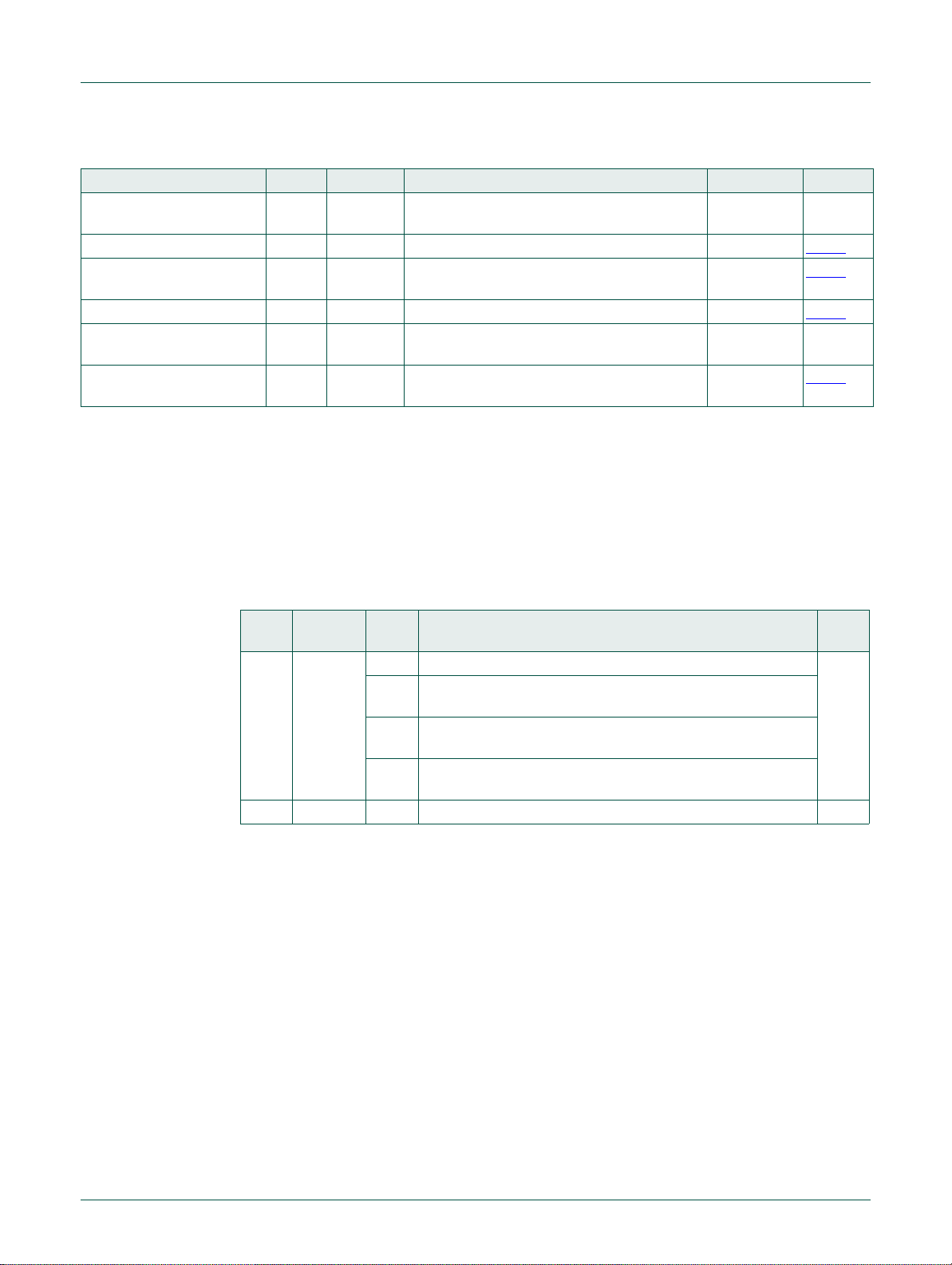
NXP Semiconductors
UM11029
Chapter 8: LPC84x System configuration (SYSCON)
Table 125. Register overview: System configuration (base address 0x4004 8000) …continued
Name Access Offset Description Reset value Section
- - 0x218 0x22C
PDSLEEPCFG R/W 0x230 Power-down states in deep-sleep mode 0xFFFF 8.6.45
PDAWAKECFG R/W 0x234 Power-down states for wake-up from
PDRUNCFG R/W 0x238 Power configuration register 0xEDF8 8.6.47
- - 0x23C 0x3F4
DEVICE_ID R 0x3F8 Device ID part
Reserved - -
0xEDF8 8.6.46
deep-sleep
Reserved - -
8.6.48
dependent
8.6.1 System memory remap register
The system memory remap register selects whether the exception vectors are read from
boot ROM, flash, or SRAM. By default, the flash memory is mapped to address
0x0000 0000. When the MAP bits in the SYSMEMREMAP register are set to 0x0 or 0x1,
the boot ROM or RAM respectively are mapped to the bottom 512 bytes of the memory
map (addresses 0x0000 0000 to 0x0000 0200).
Table 126. System memory remap register (SYSMEMREMAP, address 0x4004 8000) bit
description
Bit Symbol Value Description Reset
value
1:0 MAP System memory remap. Value 0x3 is reserved. 0x2
0x0 Bootloader Mode. Interrupt vectors are re-mapped to Boot
ROM.
0x1 User RAM Mode. Interrupt vectors are re-mapped to Static
RAM.
0x2 User Flash Mode. Interrupt vectors are not re-mapped and
reside in Flash.
31:2 - - Reserved -
8.6.2 System PLL control register
This register connects and enables the system PLL and configures the PLL multiplier and
divider values. The PLL accepts an input frequency from 10 MHz to 25 MHz from various
clock sources. The input frequency is multiplied to a higher frequency and then divided
down to provide the actual clock used by the CPU, peripherals, and memories. The PLL
can produce a clock up to the maximum allowed for the CPU.
Remark: The divider values for P and M must be selected so that the PLL output clock
frequency FCLKOUT is lower than 100 MHz.
UM11029 All information provided in this document is subject to legal disclaimers. © NXP Semiconductors N.V. 2017. All rights reserved.
User manual Rev. 1.0 — 16 June 2017 89 of 515
Page 90

NXP Semiconductors
Table 127. System PLL control register (SYSPLLCTRL, address 0x4004 8008) bit description
Bit Symbol Value Description Reset
4:0 MSEL Feedback divider value. The division value M is the
6:5 PSEL Post divider ratio P. The division ratio is 2 P. 0
31:7 - - Reserved. Do not write ones to reserved bits. -
8.6.3 System PLL status register
This register is a Read-only register and supplies the PLL lock status (see
Section 8.7.3.1
Table 128. System PLL status register (SYSPLLSTAT, address 0x4004 800C) bit des cription
Bit Symbol Value Description Reset
0 LOCK PLL lock status 0
31:1 - - Reserved -
UM11029
Chapter 8: LPC84x System configuration (SYSCON)
value
0
programmed MSEL value + 1.
00000: Division ratio M = 1
to
11111: Div i s i o n r a t i o M = 32
0x0 P = 1
0x1 P = 2
0x2 P = 4
0x3 P = 8
).
value
0 PLL not locked
1 PLL locked
8.6.4 System oscillator control register
This register configures the frequency range for the system oscillator. The system
oscillator itself is powered on or off in the PDRUNCFG register. See Tab le 1 72
Table 129. System oscillator control register (SYSOSCCTRL, address 0x4004 8020) bit
description
Bit Symbol Value Description Reset
0 BYPASS Bypass system oscillator 0x0
0 Disabled. Oscillator is not bypassed.
1 Enabled. PLL input (sys_osc_clk) is fed directly
from the XTALIN pin bypassing the oscillator. Use
this mode when using an external clock source
instead of the crystal oscillator.
1 FREQRANGE Determines oscillator frequency range. 0x0
0 1 - 20 MHz frequency range.
1 15 - 25 MHz frequency range
31:2 - - Reserved 0x00
UM11029 All information provided in this document is subject to legal disclaimers. © NXP Semiconductors N.V. 2017. All rights reserved.
User manual Rev. 1.0 — 16 June 2017 90 of 515
.
value
Page 91

NXP Semiconductors
8.6.5 Watchdog oscillator control register
This register configures the watchdog oscillator. The oscillator consists of an analog and a
digital part. The analog part contains the oscillator function and generates an analog clock
(Fclkana). With the digital part, the analog output clock can be divided to the required
output clock frequency wdt_osc_clk. The analog output frequency (Fclkana) can be
adjusted with the FREQSEL bits between 600 kHz and 4.6 MHz. With the digital part
Fclkana will be divided (divider ratios = 2, 4,...,64) to wdt_osc_clk using the DIVSEL bits.
The output clock frequency of the watchdog oscillator can be calculated as
wdt_osc_clk = Fclkana/(2 (1 + DIVSEL)) = 9.3 kHz to 2.3 MHz (nominal values).
Remark: Any setting of the FREQSEL bits will yield a Fclkana value within 40% of the
listed frequency value. The watchdog oscillator is the clock source with the lowest power
consumption. If accurate timing is required, use the FRO or system oscillator.
Remark: The frequency of the watchdog oscillator is undefined after reset. The watchdog
oscillator frequency must be programmed by writing to the WDTOSCCTRL register before
using the watchdog oscillator.
Table 130. Watchdog oscillator control register (WDTOSCCTRL, address 0x4004 8024) bit
Bit Symbol Value Description Reset
4:0 DIVSEL Select divider for Fclkana.
8:5 FREQSEL Select watchdog oscillator analog output frequency
31:9 - - Reserved 0x00
UM11029
Chapter 8: LPC84x System configuration (SYSCON)
description
value
0
wdt_osc_clk = Fclkana/ (2 (1 + DIVSEL))
00000: 2 (1 + DIVSEL) = 2
00001: 2 (1 + DIVSEL) = 4
to
11111: 2 (1 + DIVSEL) = 64
0x00
(Fclkana).
0x0 0 MHz
0x1 0.6 MHz
0x2 1.05 MHz
0x3 1.4 MHz
0x4 1.75 MHz
0x5 2.1 MHz
0x6 2.4 MHz
0x7 2.7 MHz
0x8 3.0 MHz
0x9 3.25 MHz
0xA 3.5 MHz
0xB 3.75 MHz
0xC 4.0 MHz
0xD 4.2 MHz
0xE 4.4 MHz
0xF 4.6 MHz
UM11029 All information provided in this document is subject to legal disclaimers. © NXP Semiconductors N.V. 2017. All rights reserved.
User manual Rev. 1.0 — 16 June 2017 91 of 515
Page 92

NXP Semiconductors
8.6.6 FRO oscillator control register
The FROOSCCTRL register can be used to select direct fro_oscout (30 MHz, 24 MHz,
18 MHz) or select divided fro_oscout (1.125 MHz, 1.5 MHz, 1.875 MHz, 9 MHz, 12 MHz,
or 15 MHz) based on FAIM low power boot value.
UM11029
Chapter 8: LPC84x System configuration (SYSCON)
The set_fro_frequency API call (Chapter 9 “
used to select desired output frequency from FRO. See Figure 9 “
LPC84x FRO API ROM routine”) must be
UM11029 clock
generation (continued)”.
Table 131. FRO oscillator control register (FROOSCCTRL, address 0x4004 8028) bit description
Bit Symbol Value Description Reset
16:0 - Reserved 0
17 FRO_DIRECT FRO direct clock select 0
31:18 - - Reserved -
0
1 FRO clock is direct from FRO oscillator
fro_oscout is divided by 2 (normal boot) or 16 (low power
boot), depending on FAIM low power boot value. See
Section 4.2.1 “
FAIM bit definitions”.
value
8.6.7 FRO direct clock source update register
The FRODIRECTCLKUEN register updates the clock source of the FRO clock with the
new input clock after the FROOSCCTRL register bit 17 has been written to. In order for
the update to take effect, first write a zero to the FRODIRECTCLKUEN register and then
write a one to FRODIRECTCLKUEN.
Table 132. FRO direct clock source update enable register (FRODIRECTCLKUEN, address 0x4004 8030) bit
description
Bit Symbol Value Description Reset
0 ENA Enable FRO clock source update. 0
31:1 - - Reserved -
value
0 No change
1 Update clock source
UM11029 All information provided in this document is subject to legal disclaimers. © NXP Semiconductors N.V. 2017. All rights reserved.
User manual Rev. 1.0 — 16 June 2017 92 of 515
Page 93

NXP Semiconductors
8.6.8 System reset status register
The SYSRSTSTAT register shows the source of the latest reset event. The bits are
cleared by writing a one to any of the bits. The POR event clears all other bits in this
register. If another reset signal - for example the external RESET
after the POR signal is negated, then its bit is set to detected. Write a one to clear the
reset.
UM11029
Chapter 8: LPC84x System configuration (SYSCON)
pin - remains asserted
The reset value given in Table 133
Table 133. System reset status register (SYSRSTSTAT, address 0x4004 8038) bit description
Bit Symbol Value Description Reset
0 POR POR reset status 0
0 No POR detected
1 POR detected. Writing a one clears this reset.
1 EXTRST Status of the external RESET
0 No reset event detected.
1 Reset detected. Writing a one clears this reset.
2 WDT Status of the Watchdog reset. 0
0 No WDT reset detected.
1 WDT reset detected. Writing a one clears this reset.
3 BOD Status of the Brown-out detect reset 0
0 No BOD reset detected
1 BOD reset detected. Writing a one clears this reset.
4 SYSRST Status of the software system reset 0
0 No System reset detected
1 System reset detected. Writing a one clears this reset.
31:5 - - Reserved -
applies to the POR reset.
value
pin. External reset status. 0
8.6.9 System PLL clock source select register
This register selects the clock source for the system PLL. The SYSPLLCLKUEN register
(see Section 8.6.10
T able 134. System PLL clock source select register (SYSPLLCLKSEL, address 0x4004 8040)
bit description
Bit Symbol Value Description Reset
1:0 SEL System PLL clock source 0
31:2 - - Reserved -
UM11029 All information provided in this document is subject to legal disclaimers. © NXP Semiconductors N.V. 2017. All rights reserved.
User manual Rev. 1.0 — 16 June 2017 93 of 515
) must be toggled from LOW to HIGH for the update to take effect.
value
0x0 FRO
0x1 External clock
0x2 Watchdog oscillator
0x3 FRO DIV
Page 94

NXP Semiconductors
8.6.10 System PLL clock source update register
This register updates the clock source of the system PLL with the new input clock after the
SYSPLLCLKSEL register has been written to. In order for the update to take effect, first
write a zero to the SYSPLLUEN register and then write a one to SYSPLLUEN.
Table 135. System PLL clock source update enable register (SYSPLLCLKUEN, address
Bit Symbol Value Description Reset value
0 ENA Enable system PLL clock source update 0
31:1 - - Reserved -
8.6.11 Main clock PLL source select register
The MAINCLKPLLSEL register selects the main system clock, which can be the system
PLL (sys_pllclkout), or the main clock pre pll. The main system clock clocks the core, the
peripherals, and the memories.
UM11029
Chapter 8: LPC84x System configuration (SYSCON)
0x4004 8044) bit description
0 No change
1 Update clock source
Bit 0 of the MAINCLKUEN register (see Section 8.6.14
) must be toggled from 0 to 1 for
the update to take effect.
Table 136. Main clock source select register (MAINCLKPLLSEL, address 0x4004 8048) bit
description
Bit Symbol Value Description Reset value
1:0 SEL Clock source for main clock 0
0x0 main_clk_pre_pll
0x1 SYS PLL
0x2 None
0x3 None
31:2 - - Reserved -
8.6.12 Main clock PLL source update enable register
.The MAINCLKPLLUEN register updates the clock source of the main clock with the new
input clock after the MAINCLKPLLSEL register has been written to. In order for the update
to take effect, first write a zero to bit 0 of this register, then write a one.
Table 137. Main clock source update enable register (MAINCLKPLLUEN, address 0x4004
804C) bit description
Bit Symbol Value Description Reset value
0 ENA Enable main clock source update. 0
0 No change
1 Update clock source
31:1 - - Reserved -
UM11029 All information provided in this document is subject to legal disclaimers. © NXP Semiconductors N.V. 2017. All rights reserved.
User manual Rev. 1.0 — 16 June 2017 94 of 515
Page 95

NXP Semiconductors
8.6.13 Main clock source select register
The MAINCLKSEL register selects the main_clock_pre_pll, which can be the FRO,
external clock, watchdog oscillator, or FRO_DIV.
UM11029
Chapter 8: LPC84x System configuration (SYSCON)
Bit 0 of the MAINCLKUEN register (Section 8.6.14
) must be toggled from 0 to 1 for the
update to take effect.
Table 138. Main clock source select register (MAINCLKSEL, address 0x4004 8050) bit
description
Bit Symbol Value Description Reset value
1:0 SEL Clock source for main clock pre pll 0
0x0 FRO
0x1 External clock
0x2 Watchdog oscillator
0x3 FRO_DIV = FRO / 2
31:2 - - Reserved -
8.6.14 Main clock source update enable register
The MAINCLKUEN register updates the clock source of the main clock with the new input
clock after the MAINCLKSEL register has been written to. In order for the update to take
effect, first write a zero to bit 0 of this register, then write a one.
Table 139. Main clock source update enable register (MAINCLKUEN, address 0x4004 80574)
bit description
Bit Symbol Value Description Reset value
0 ENA Enable main clock source update 0
0 No change
1 Update clock source
31:1 - - Reserved -
8.6.15 System clock divider register
This register controls how the main clock is divided to provide the system clock to the
core, memories, and the perispherals. The system clock can be shut down completely by
setting the DIV field to zero.
Table 140. System clock divider register (SYSAHBCLKDIV, address 0x4004 80578) bit
description
Bit Symbol Description Reset
value
7:0 DIV System AHB clock divider values
0: System clock disabled.
1: Divide by 1.
…
255: Divide by 255.
31:8 - Reserved -
UM11029 All information provided in this document is subject to legal disclaimers. © NXP Semiconductors N.V. 2017. All rights reserved.
User manual Rev. 1.0 — 16 June 2017 95 of 515
0x01
Page 96

NXP Semiconductors
8.6.16 ADC clock source select register
The ADCCLKSEL register selects the ADC clock, which can be the FRO or sys_pll.
Table 141. ADC clock source select register (ADCCLKSEL, address 0x4004 8064) bit
Bit Symbol Value Description Reset value
1:0 SEL Clock source for ADC clock. 0x0
31:3 - Reserved -
8.6.17 ADC clock divider register
The ADCCLKDIV register controls how the ADC clock is divided to provide the ADC clock
to the ADC controller. The ADC clock can be shut down completely by setting the DIV field
to zero.
Table 142. ADC clock divider register (ADCCLKDIV, address 0x4004 8068) bit description
Bit Symbol Value Description Reset value
7:0 DIV ADC clock divider values.
31:8 - Reserved -
UM11029
Chapter 8: LPC84x System configuration (SYSCON)
description
0x0 FRO
0x1 SYS PLL
0x2 None
0x3 None
0x0
0: ADC clock disabled.
1: Divide by 1.
…
255: Divide by 255.
8.6.18 SCT clock source select register
The SCTCLKSEL register selects the SCT clock, which can be the FRO, main clock or
sys_pll.
Table 143. SCT clock source select register (SCTCLKSEL, address 0x4004 806C) bit
description
Bit Symbol Value Description Reset value
1:0 SEL Clock source for SCT clock 0x0
0x0 FRO
0x1 Main clock
0x2 SYS PLL
0x3 None
31:2 - Reserved -
8.6.19 SCT clock divider register
The SCTCLKDIV register controls how the SCT clock is divided to provide the SCT clock
to the SCT module. The SCT clock can be shut down completely by setting the DIV field
to zero.
UM11029 All information provided in this document is subject to legal disclaimers. © NXP Semiconductors N.V. 2017. All rights reserved.
User manual Rev. 1.0 — 16 June 2017 96 of 515
Page 97

NXP Semiconductors
Table 144. SCT clock divider register (SCTCLKDIV, address 0x4004 8070) bit description
Bit Symbol Value Description Reset value
7:0 DIV SCT clock divider values.
31:8 - Reserved -
8.6.20 External clock source select register
The EXTCLKSEL register selects the external clock, which can be the system oscillator or
clk_in (direct from external IO).
Table 145. External clock source select register (EXTCLKSEL, address 0x4004 8074) bit
Bit Symbol Value Description Reset value
0 SEL Clock source for external clock 0x0
31:1 - Reserved -
UM11029
Chapter 8: LPC84x System configuration (SYSCON)
0x0
0: SCT clock disabled.
1: Divide by 1.
…
255: Divide by 255.
description
0x0 System oscillator
0x1 CLK_IN
8.6.21 System clock control 0 register
The SYSAHBCLKCTRL0 register enables the clocks to individual system and peripheral
blocks. The system clock (bit 0) provides the clock for the AHB, the APB bridge, the ARM
Cortex-M0+, the SYSCON block, and the PMU. This clock cannot be disabled.
Table 146. System clock control 0 register (SYSAHBCLKCTRL0, address 0x4004 8080) bit
description
Bit Symbol Value Description Reset
value
0 SYS Enables the clock for the AHB, the APB bridge, the
Cortex-M0+ core clocks, SYSCON, and the PMU.
This bit is read only and always reads as 1.
1 ROM Enables clock for ROM. 1
0 Disable
1 Enable
2 RAM0_1 Enables clock for SRAM0 and SRAM1. 1
0 Disable
1 Enable
3 Reserved 0
4 FLASH Enables clock for flash. 1
0 Disable
1 Enable
5 I2C0 Enables clock for I2C0. 0
0 Disable
1 Enable
UM11029 All information provided in this document is subject to legal disclaimers. © NXP Semiconductors N.V. 2017. All rights reserved.
User manual Rev. 1.0 — 16 June 2017 97 of 515
1
Page 98

NXP Semiconductors
UM11029
Chapter 8: LPC84x System configuration (SYSCON)
Table 146. System clock control 0 register (SYSAHBCLKCTRL0, address 0x4004 8080) bit
description
Bit Symbol Value Description Reset
6 GPIO0 Enables clock for GPIO0 port registers. 0
7 SWM Enables clock for switch matrix. 1
8 SCT Enables clock for state configurable timer
9 WKT Enables clock for self-wake-up timer. 0
10 MRT Enables clock for multi-rate timer.
11 SPI0 Enables clock for SPI0. 0
12 SPI1 Enables clock for SPI1.
13 CRC Enables clock for CRC. 0
14 UART0 Enables clock for USART0. 0
15 UART1 Enables clock for USART1. 0
16 UART2 Enables clock for USART2. 0
17 WWDT Enables clock for WWDT. 0
18 IOCON Enables clock for IOCON block. 0
UM11029 All information provided in this document is subject to legal disclaimers. © NXP Semiconductors N.V. 2017. All rights reserved.
User manual Rev. 1.0 — 16 June 2017 98 of 515
…continued
value
0 Disable
1 Enable
0 Disable
1 Enable
0
SCTimer/PWM.
0 Disable
1 Enable
0 Disable
1 Enable
0 Disable
1 Enable
0 Disable
1 Enable
0 Disable
1 Enable
0 Disable
1 Enable
0 Disable
1 Enable
0 Disable
1 Enable
0 Disable
1 Enable
0 Disable
1 Enable
0 Disable
1 Enable
Page 99

NXP Semiconductors
Table 146. System clock control 0 register (SYSAHBCLKCTRL0, address 0x4004 8080) bit
Bit Symbol Value Description Reset
19 ACMP Enables clock to analog comparator. 0
20 GPIO1 Enables clock for GPIO1 port registers. 0
21 I2C1 Enables clock to I2C1. 0
22 I2C2 Enables clock to I2C2. 0
23 I2C3 Enables clock to I2C3. 0
24 ADC Enables clock to ADC. 0
25 CTIMER0 - Enables clock for CTIMER0 0
26 MTB Enables clock to micro-trace buffer control registers.
27 DAC0 - Enable clock for DAC0 0
28 GPIO_INT Enable clock for GPIO pin interrupt registers. 0
29 DMA Enables clock to DMA. 0
30 UART3 Enable clock for UART3 0
description
UM11029
Chapter 8: LPC84x System configuration (SYSCON)
…continued
value
0 Disable
1 Enable
0 Disable
1 Enable
0 Disable
1 Enable
0 Disable
1 Enable
0 Disable
1 Enable
0 Disable
1 Enable
0 Disable
1 Enable
0
Turn on this clock when using the micro-trace buffer
for debug purposes.
0 Disable
1 Enable
0 Disable
1 Enable
0 Disable
1 Enable
0 Disable
1 Enable
0 Disable
1 Enable
UM11029 All information provided in this document is subject to legal disclaimers. © NXP Semiconductors N.V. 2017. All rights reserved.
User manual Rev. 1.0 — 16 June 2017 99 of 515
Page 100

NXP Semiconductors
Table 146. System clock control 0 register (SYSAHBCLKCTRL0, address 0x4004 8080) bit
Bit Symbol Value Description Reset
31 UART4 Enable clock for UART4 0
8.6.22 System clock control 1 register
The SYSAHBCLKCTRL1 register enables the clocks to peripheral blocks.
Table 147. System clock control 1 register (SYSAHBCLKCTRL1, address 0x4004 8084) bit
Bit Symbol Value Description Reset
0 - Reserved 0
1 DAC1 Enables clock for DAC1. 0
31:2 - Reserved -
description
description
UM11029
Chapter 8: LPC84x System configuration (SYSCON)
…continued
value
0 Disable
1 Enable
value
0 Disable
1 Enable
8.6.23 Peripheral reset control 0 register
The PRESET0CTRL register allows software to reset specific peripherals. A zero in any
assigned bit in this register resets the specified peripheral. A 1 clears the reset and allows
the peripheral to operate.
Table 148. Peripheral reset control 0 register (PRESETCTRL0, address 0x4004 8088) bit description
Bit Symbol Value Description Reset
3:0 - Reserved 1
4 FLASH_RST_N Flash controller reset control 1
5 I2C0_RST_N I
6 GPIO0_RST_N GPIO0 reset control 1
7 SWM_RST_N SWM reset control 1
8 SCT_RST_N SCT reset control 1
0 Assert the flash controller reset.
1 Clear the flash controller reset.
2
C0 reset control 1
2
0 Assert the I
1 Clear the I
C0 reset.
2
C0 reset.
0 Assert the GPIO0 reset
1 Clear the GPIO0 reset.
0 Assert the SWM reset.
1 Clear the SWM reset.
0 Assert the SCT reset.
1 Clear the SCT reset.
value
UM11029 All information provided in this document is subject to legal disclaimers. © NXP Semiconductors N.V. 2017. All rights reserved.
User manual Rev. 1.0 — 16 June 2017 100 of 515
 Loading...