

NXP Semiconductors LPC824M201JHI33, LPC822M101JHI33, LPC824M201JDH20, LPC822M101JDH20 User Manual
Page 1
UM10800
LPC82x User manual
Rev. 1.2 — 5 October 2016 User manual
Document information
Info Content
Keywords LPC82x, LPC824M201JHI33, LPC822M101JHI33, LPC824M201JDH20,
LPC822M101JDH20, LPC82x UM, LPC82x user manual, LPC820
Abstract LPC82x User manual
Page 2

NXP Semiconductors
UM10800
LPC82x User manual
Revision history
Rev Date Description
1.2 20161005 LPC82x User manual.
Modifications: • Updated Table 383 “Error codes”: added error codes 0x0006 0009 and 0x0006 000A.
• Added bits: 24 - ADC_RST_N; 29 - DMA_RST_N to Table 23 “Peripheral reset control register
(PRESETCTRL, address 0x4004 8004) bit description”.
• Added Section 12.5.7 “Channel chaining”.
1.1 20160524 LPC82x User manual.
Modifications: • Removed internal comments from Section 16.6.24 “SCT event enable registers 0 to 7”
• Changed main clock to system clock in the first paragraph in Section 26.5.1.1 “Param0: system PLL
input frequency and Param1: expected system clock”.
• Updated Section 25.6.2 “IAP commands”.
• Updated Table 308 “LPC82x flash configuration”: corrected the page num be rs of secto rs 21 - 31.
• Updated Section 16.6 “Register description” to fix the polarity for REGMODE.
– REGMODEn = 0: Registers operate as match and reload registers.
– REGMODEn = 1: Registers operate as capture and capture control registers.
• Changed signature generation start address (corresponds to AHB byte address bits[20:4]) to
signature generation start address (corresponds to AHB byte address bits[18:2]).
• Added a note to Table 236 “SCT DMA 0 request register (DMAREQ0, address 0x5000 405C) bit
description” and Table 237 “SCT DMA 1 request register (DMAREQ1, address 0x5000 C060) bit
description”.
• Changed the ISP entry pin in Section 31.5.2 “Debug connections for SWD” to PIO0_20; was
PIO0_1.
• Added reserved blocks in Table 222 “Register overview: State Configurable Timer SCT/PWM (base
address 0x5000 4000)”: 0x220 to 0x2FF before EV0_STATE 0x340 to 0x4FF before OUT0_SET
1 20140918 Initial revision. LPC82x User manual.
Contact information
For more information, please visit: http://www.nxp.com
For sales office addresses, please send an email to: salesaddresses@nxp.com
UM10800 All information provided in this document is subject to legal disclaimers. © NXP Semiconductors N.V. 2016. All rights reserved.
User manual Rev. 1.2 — 5 October 2016 2 of 487
Page 3

1.1 Introduction
UM10800
Chapter 1: LPC82x Introductory information
Rev. 1.2 — 5 October 2016 User manual
The LPC82x are an ARM Cortex-M0+ based, low-cost 32-bit MCU family operating at
CPU frequencies of up to 30 MHz. The LPC82x support up to 32 KB of flash memory and
8 KB of SRAM.
2
The peripheral complement of the LPC82x includes a CRC engine, four I
interfaces, up to three USARTs, up to two SPI interfaces, one multi-rate timer,
self-wake-up timer, and state-configurable timer with PWM function (SCTimer/PWM), a
DMA, one 12-bit ADC and one analog comp arator, function-configurable I/O port s through
a switch matrix, an input pattern match engine, and up to 29 general-purpose I/O pins.
C-bus
1.2 Features
Remark: For additional documentation, see Section 35.2 “References”
.
• System:
– ARM Cortex-M0+ processor (revision r0p1), running at frequencies of up to
30 MHz with single-cycle multiplier and fast single-cycle I/O port.
– ARM Cortex-M0+ built-in Nested Vectored Interrupt Controller (NVIC).
– System tick timer.
– AHB multilayer matrix.
– Serial Wire Debug (SWD) with four break points and two watch points. JTAG
boundary scan (BSDL) supported.
– Micro Trace Buffer (MTB)
• Memory:
– Up to 32 KB on-chip flash programming memory with 64 Byte page write and
erase. Code Read Protection (CRP) supported.
– 8 KB SRAM.
• ROM API support:
– bootloader.
– On-chip ROM APIs for ADC, SPI, I2C, USART, power configuration (power
profiles) and integer divide.
– Flash In-A pp licatio n Pro gr a mm in g (IAP ) an d In- Sys te m Pro gr a mmin g (ISP).
• Digital peripherals:
– High-spe e d GPI O in te r fac e co nn ec te d to the ARM Cort ex -M 0 + IO bu s wit h up t o
32 General-Purpose I/O (GPIO) pins with configurable pull-up/pull-down resistors,
programmable open-drain mode, input inverter, and glitch filter. GPIO direction
control supports independent set/clear/toggle of individual bits.
– High-current source output driver (20 mA) on four pins.
– High-current sink driver (20 mA) on two true open-drain pins.
UM10800 All information provided in this document is subject to legal disclaimers. © NXP Semiconductors N.V. 2016. All rights reserved.
User manual Rev. 1.2 — 5 October 2016 3 of 487
Page 4

NXP Semiconductors
Chapter 1: LPC82x Introductory information
– GPIO interrupt generation capability with boolean pattern-matching feature on
eight GPIO inputs.
– Switch matrix for flexible configuration of each I/O pin function.
– CRC engine.
– DMA with 18 channels and 9 trigger inputs.
UM10800
• Timers:
– State Configurable Timer (SCTimer/PWM) with input and output functions
(including capture and match) for timing and PWM applica tio ns .
– Four channel Multi-Rate Timer (MRT) for repetitive interrupt generation at up to
four programmable, fixed rates.
– Self-Wake-up Timer (WKT) clocked from either the IRC, a low-power,
low-frequency internal oscillator, or an external clock input in the always-on power
domain.
– Windowed Watchdog timer (WWDT).
• Analog peripherals:
– One 12-bit ADC with up to 12 input channels with multiple internal and external
trigger inputs and with sample rates of up to 1.2 Msamples/s. The ADC supports
two independent conversion sequences.
– Comparator with four input pins and external or internal reference voltage.
• Serial peripherals:
– Three USART interfaces with pin functions assigned through the switch matrix and
one common fractional baud rate generator.
– Two SPI controllers with pin functions assigned through the switch matrix.
2
– Four I
on two true open-drain pins and listen mode. Three I2Cs support data rates up to
400 kbit/s on standard digital pins.
C-bus interfaces. One I2C supports Fast-mode plus with 1 Mbit/s data rates
• Clock generation:
– 12 MHz internal RC oscillator trimmed to 1.5 % accuracy that can optionally be
used as a system clock.
– Crystal oscillator with an operating range of 1 MHz to 25 MHz.
– Programmable watchdog oscillator with a frequency range of 9.4 kHz to 2.3 MHz.
– PLL allows CPU operation up to the maximum CPU rate without the need for a
high-frequency crystal. May be run from the system oscillator, the external clock
input, or the internal RC oscillator.
– Clock output function with divider that can reflect all internal clock sources.
• Power control:
– Integrated PMU (Power Management Unit) to minimize power consumption.
– Reduced power modes: Sleep mode, Deep-sleep mode, Power-down mode, and
Deep power-down mode.
– Wake-up from Deep-sleep and Power-down modes on activity on USART, SPI,
and I2C peripherals.
– Timer-controlled self-wake-up from Deep power-down mode.
– Power-On Reset (POR).
UM10800 All information provided in this document is subject to legal disclaimers. © NXP Semiconductors N.V. 2016. All rights reserved.
User manual Rev. 1.2 — 5 October 2016 4 of 487
Page 5
NXP Semiconductors
– Brownout detect (BOD).
• Unique device serial number for identification.
• Single power supply (1.8 V to 3.6 V).
• Operating temperature range -40 °C to +105 °C.
• Available in a HVQFN33 (5x5) package.
1.3 Ordering options
UM10800
Chapter 1: LPC82x Introductory information
Table 1. Ordering information
Type number Package
LPC824M201JHI33 HVQFN33 HVQFN: plastic thermal enhanced very thin quad flat package; no leads;
LPC822M101JHI33 HVQFN33 HVQFN: plastic thermal enhanced very thin quad flat package; no leads;
LPC824M201JDH20 TSSOP20 plastic thin shrink small outline package; 20 leads; body width 4.4 mm SOT360-1
LPC822M101JDH20 TSSOP20 plastic thin shrink small outline package; 20 leads; body width 4.4 mm SOT360-1
Table 2. Ordering options
Type number Flash/KBSRAM/KBUSART I2C SPI ADC
LPC824M201JHI33 32 8 3 4 2 12 Y 29 HVQFN33
LPC822M101JHI33 16 4 3 4 2 12 Y 29 HVQFN33
LPC824M201JDH20 32 8 3 4 2 5 Y 16 TSSOP20
LPC822M101JDH20 16 4 3 4 2 5 y 16 TSSOP20
Name Description Version
n/a
33 terminals; body 5 5 0.85 mm
n/a
33 terminals; body 5 5 0.85 mm
Comparator GPIO Package
channels
1.4 General description
1.4.1 ARM Cortex-M0+ core configuration
The ARM Cortex-M0+ core runs at an operating frequency of up to 30 MHz. Integrated in
the core are the NVIC and Serial Wire Debug with four breakpoints and two watch points.
The ARM Cortex-M0+ core supports a single-cycle I/O enabled port (IOP) for fast GPIO
access at address 0xA000 0000. The ARM Cortex M0+ core version is r0p1.
The core includes a single-cycle multiplier and a system tick timer (SysTick).
UM10800 All information provided in this document is subject to legal disclaimers. © NXP Semiconductors N.V. 2016. All rights reserved.
User manual Rev. 1.2 — 5 October 2016 5 of 487
Page 6
NXP Semiconductors
1.5 Block diagram
UM10800
Chapter 1: LPC82x Introductory information
LPC82xM
29 x
SWITCH
MATRIX
SWCLK, SWD
29 x
PIO0
HIGH-SPEED
PIN INTERRUPTS/
PATTERN MATCH
SCT_PIN[3:0]
SCT_OUT[6:0]
TXD, RTS
RXD, CTS
SCLK
SCK, SSEL
MISO, MOSI
SCL
SDA
XTALOUT
XTALIN
RESET, CLKIN
CLKOUT
GPIO
SCTIMER/
INPUT MUX
USART0/1/2
SPI0/1
I2C0/1/2/3
XTAL
PWM
TEST/DEBUG
INTERFACE
CORTEX-M0+
slave
AHB TO APB
SYSCON
ARM
BRIDGE
FLASH
16/32 KB
slave slave
AHB-LITE BUS
slave master
MULTI-RATE TIMER
ALWAYS-ON POWER DOMAIN
SRAM
4/8 KB
CRC
WWDT
IOCON
PMU
SELF
WAKE-UP TIMER
slave
DMA
ROM
ADC_[11:0]
ACMP_I[4:1]
VDDCMP
ACMP_O
ADC
COMPARATOR
IRC
WDOsc
BOD
POR
CLOCK
GENERATION,
POWER CONTROL,
SYSTEM
FUNCTIONS
clocks and
controls
aaa-014399
Grey-shaded blocks show peripherals that can provide hardware triggers for DMA transfers or
have DMA request lines.
Fig 1. LPC82x block diagram
UM10800 All information provided in this document is subject to legal disclaimers. © NXP Semiconductors N.V. 2016. All rights reserved.
User manual Rev. 1.2 — 5 October 2016 6 of 487
Page 7

UM10800
Chapter 2: LPC82x memory mapping
Rev. 1.2 — 5 October 2016 User manual
2.1 How to read this chapter
The memory mapping is identical for all LPC82x parts. Different LPC82x parts support
different flash and SRAM memory sizes.
2.2 General description
The LPC82x incorporates several distinct memory regions. Figure 2 shows the overall
map of the entire address space from the user program viewpoint following reset.
The APB peripheral area is 512 KB in size and is divided to allow for up to 32 peripher als.
Each peripheral is allocated 16 KB of space simplifying the address decoding.
The registers incorporated into the ARM Cortex-M0+ core, such as NVIC, SysTick, and
sleep mode control, are located on the private pe rip h er al bus.
The GPIO port and pin interrupt/pattern match registers are accessed by the ARM
Cortex-M0+ single-cycle I/O enabled port (IOP).
UM10800 All information provided in this document is subject to legal disclaimers. © NXP Semiconductors N.V. 2016. All rights reserved.
User manual Rev. 1.2 — 5 October 2016 7 of 487
Page 8
NXP Semiconductors
2.2.1 Memory mapping
UM10800
Chapter 2: LPC82x memory mapping
4 GB
1 GB
0.5 GB
0 GB
LPC82x
reserved
private peripheral bus
reserved
GPIO PINT
GPIO
reserved
DMA
SCTimer/PWM
CRC
reserved
APB peripherals
reserved
reserved
12 KB boot ROM
reserved
4 KB MTB registers
reserved
4 KB SRAM1
4 KB SRAM0
reserved
32 KB on-chip flash
0xFFFF FFFF
0xE010 0000
0xE000 0000
0xA000 8000
0xA000 4000
0xA000 0000
0x5000 C000
0x5000 8000
0x5000 4000
0x5000 0000
0x4008 0000
0x4000 0000
0x2000 0000
0x1FFF 3000
0x1FFF 0000
0x1400 1000
0x1400 0000
0x1001 2000
0x1000 1000
0x1000 0000
0x0000 8000
0x0000 0000
APB peripherals
30 - 31 reserved
29
28
27
26
25
24
23
22
21
20
19
system control (SYSCON)
18
17
16
15
14
13
12
11
10
9
8
7
6
5
4
3
2
1
0
active interrupt vectors
flash controller
DMA TRIGMUX
analog comparator
self wake-up timer
I2C3
I2C2
USART2
USART1
USART0
reserved
SPI1
SPI0
I2C1
I2C0
reserved
IOCON
reserved
reserved
reserved
reserved
input mux
PMU
12-bit ADC
reserved
reserved
reserved
switch matrix
MRT
WWDT
0x0000 00C0
0x0000 0000
0x4008 0000
0x4007 8000
0x4007 4000
0x4007 0000
0x4006 C000
0x4006 8000
0x4006 4000
0x4006 0000
0x4005 C000
0x4005 8000
0x4005 4000
0x4005 0000
0x4004 C000
0x4004 8000
0x4004 4000
0x4004 0000
0x4003 C000
0x4003 8000
0x4003 4000
0x4003 0000
0x4002 C000
0x4002 8000
0x4002 4000
0x4002 0000
0x4001 C000
0x4001 8000
0x4001 4000
0x4001 0000
0x4000 C000
0x4000 8000
0x4000 4000
0x4000 0000
The private peripheral bus includes the ARM Cortex-M0+ peripherals such as the NVIC, SysTick, and the core control registers.
Fig 2. LPC82x Memory mapping
2.2.2 Micro Trace Buffer (MTB)
The LPC82x supports the ARM Cortex-M0+ Micro Trace Buffer. See Section 31.5.4.
UM10800 All information provided in this document is subject to legal disclaimers. © NXP Semiconductors N.V. 2016. All rights reserved.
User manual Rev. 1.2 — 5 October 2016 8 of 487
Page 9

UM10800
Chapter 3: LPC82x Boot ROM
Rev. 1.2 — 5 October 2016 User manual
3.1 How to read this chapter
The bootloader is identical for all parts.
3.2 Features
• 12 KB on-chip boot ROM
• Contains the bootloader with In-System Programming (ISP) facility and the following
APIs:
– In-Application Programming (IAP) of flash memory
– Power profiles for optimizing power consumption and system performance
– USART driver
– ADC driver
– SPI driver
– I2C driver
– Integer divide routines
3.3 Basic configuration
The clock to the ROM is enabled by default. No configuration is required to use the ROM
APIs.
3.4 Pin description
When the ISP entry pin is pulled LOW on reset, the part enters ISP mode and the ISP
command handler starts up. In ISP mode, pin PIO0_0 is connected to function U0_RXD
and pin PIO0_4 is connected to function U0_TXD on the USART0 block.
Table 3. Pin location in ISP mode
ISP entry pin USART RXD USART TXD
PIO0_12 PIO0_0 PIO0_4
3.5 General description
3.5.1 Bootloader
The bootloader controls initial operation after reset and also provides the means to
accomplish programming of the flash memory via USART. This could be initial
programming of a blank device, erasure and re-programming of a previously programmed
device, or programming of the flash memory by the application program in a running
system.
UM10800 All information provided in this document is subject to legal disclaimers. © NXP Semiconductors N.V. 2016. All rights reserved.
User manual Rev. 1.2 — 5 October 2016 9 of 487
Page 10

NXP Semiconductors
The bootloader code is executed every time the part is powered on or reset. The
bootloader can execute the ISP command handler or the user application code. A LOW
level after reset at the ISP entry pin is consider ed as an external ha rdware requ est to st art
the ISP command handler via USART.
UM10800
Chapter 3: LPC82x Boot ROM
For details on the boot process, see Section 3.6.2 “
Remark: SRAM location 0x1000 0000 to 0x1000 0050 is not used by the bootloader and
the memory content in this area is retained during reset. SRAM memory is not retained
when the part powers down or enters Deep power-down mode.
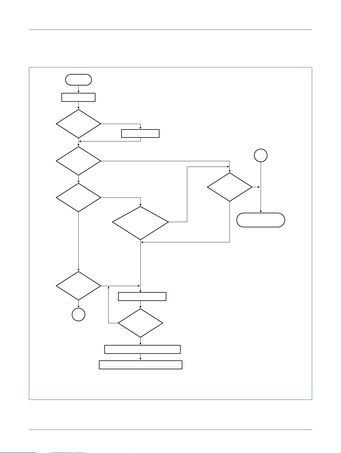
Assuming that power supply pins are at their nominal levels when the rising edge on
RESET
the decision whether to continue with user code or ISP handler is made. The bootloader
performs the following steps (see Figure 4
Remark: The sampling of pin the ISP entry pin can be disabled through programming
flash location 0x0000 02FC (see Section 25.5.3 “
pin is generated, it may take up to 3 ms before the ISP entry pin is sampled and
1. If the watchdog overflow flag is set, the bootloader checks whether a valid user code
is present. If the watchdog overflow flag is not set, the ISP entry pin is checked.
2. If there is no request for the ISP command handler execution (ISP entry pin is
sampled HIGH after reset), a search is made for a valid user program.
3. If a valid user program is found then th e exec ution contr ol is transferred to it. If a valid
user program is not found, the bootloader attempts to load a valid user program via
the USART interface.
3.5.2 ROM-based APIs
Boot process”.
):
Code Read Protection (CRP)”).
Once the part has booted, the user can access several APIs located in the boot ROM to
access the flash memory, optimize power consumption, and operate the USART and I2C
peripherals.
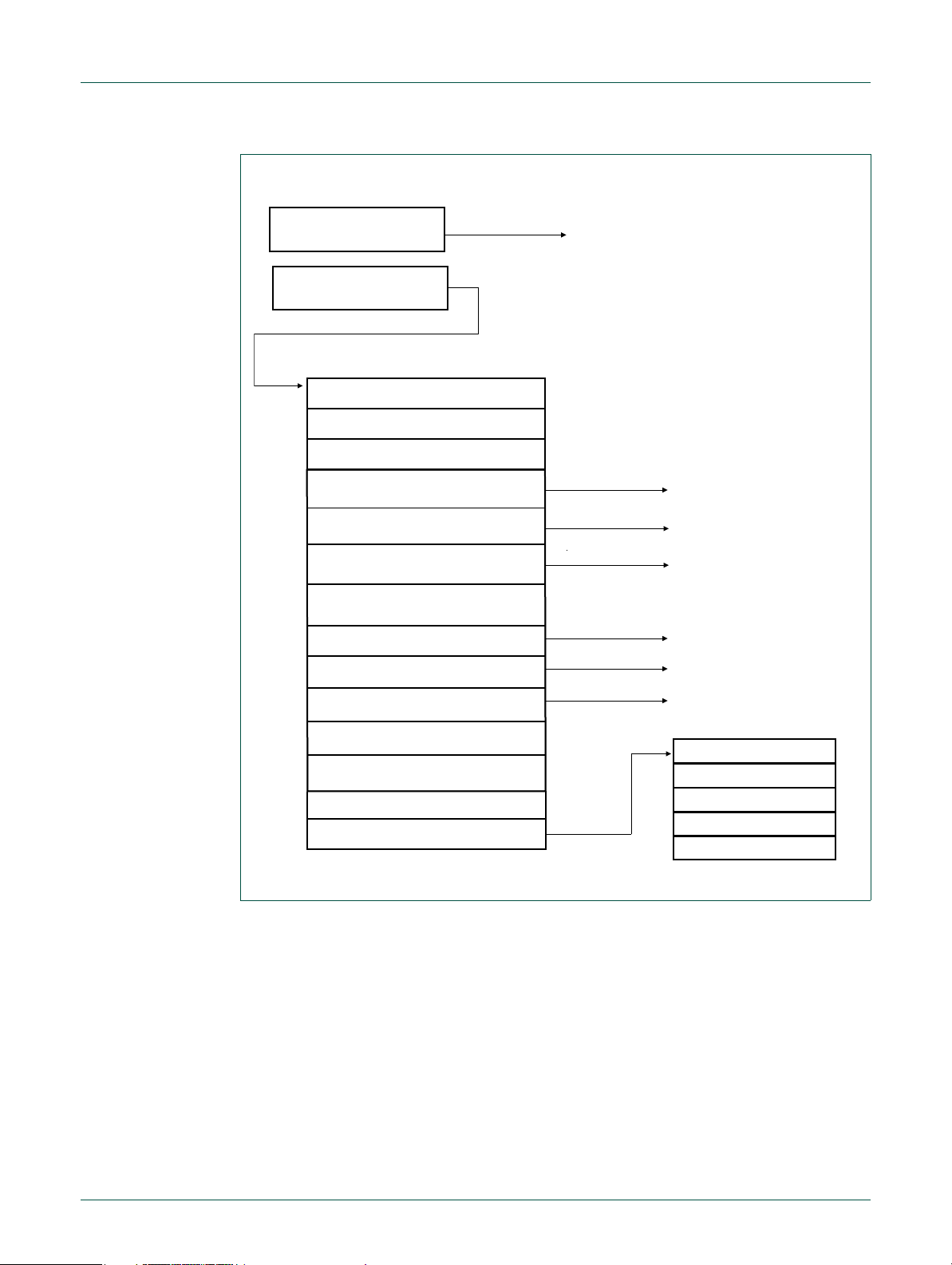
The structure of the boot ROM APIs is shown in Figure 3
.
UM10800 All information provided in this document is subject to legal disclaimers. © NXP Semiconductors N.V. 2016. All rights reserved.
User manual Rev. 1.2 — 5 October 2016 10 of 487
Page 11
NXP Semiconductors
Ptr to ROM Driver table
Reserved
Reserved
Reserved
…
Ptr to Device Table n
Ptr to Function 2
Ptr to Function 0
Ptr to Function 1
…
Ptr to Function n
Device n
ROM Driver Table
0x1FFF 1FF8
+0x0
+0x4
+0x8
+0x10
+0x14
+0xC
Device 3
Power profiles API function table
IAP calls
Ptr to IAP
0x1FFF 1FF1
Pointer to power profiles
function table
+0x18
Device 7
SPI driver routines function table
Device 8
ADC driver routines function table
Device 9
USART driver routines function table
Reserved
+0x1C
Pointer to SPI driver function table
+0x20
Pointer to ADC driver function table
+0x24
Pointer to USART driver
routines function table
+0x28
Reserved
+0x2C
Reserved
Device 4
Integer Divide routines function table
Pointer to 32-bit integer divide routines
Pointer to I2C driver routine function
table
Device 5
I2C driver routines function table
UM10800
Chapter 3: LPC82x Boot ROM
UM10800 All information provided in this document is subject to legal disclaimers. © NXP Semiconductors N.V. 2016. All rights reserved.
User manual Rev. 1.2 — 5 October 2016 11 of 487
Fig 3. Boot ROM structure
Page 12

NXP Semiconductors
The boot rom structure should be included as follows:
typedef struct {
} LPC_ROM_API_T;
#define ROM_DRIVER_BASE (0x1FFF1FF8UL)
Table 4. API calls
API Description Reference
Flash IAP Flash In-Application programming Table 330
Power profiles API Configure system clock and power consumption Table 343
Integer divide routines 32-bit integer divide routines Table 399
I2C driver I2C ROM driver Table 364
SPI driver SPI ROM driver Table 356
ADC driver ADC ROM driver Table 385
UART driver USART ROM driver Table 346
UM10800
Chapter 3: LPC82x Boot ROM
const uint32_t reserved0; /*!< Reserved */
const uint32_t reserved1; /*!< Reserved */
const uint32_t reserved2; /*!< Reserved */
const PWRD_API_T *pPWRD; /*!< Power API function table base address */
const ROM_DIV_API_T *divApiBase; /*!< Divider API function table base address */
const I2CD_API_T *pI2CD;/*!< I2C driver routines functions table */
const uint32_t reserved5; /*!< Reserved */
const SPID_API_T *pSPID; /*!< SPI driver API function table base address */
const ADCD_API_T *pADCD; /*!< ADC driver API function table base address */
const UARTD_API_T *pUARTD; /*!< USART driver API function table base address */
3.6 Functional description
3.6.1 Memory map after any reset
The boot block is 12 KB in size. The boot block is located in the memory region starting
from the address 0x1FFF 0000. The bootloader is designed to run from this memory area,
but both the ISP and IAP software use parts of the on-chip RAM. The RAM usage is
described in Section 25.7.2 “
vectors residing in the boot block of the on-chip flash memory also become active after
reset, i.e., the bottom 512 bytes of the boot block are also visible in the memory region
starting from the address 0x0000 0000.
3.6.2 Boot process
During the boot process, the bootloader checks if there is valid user code in flash. The
criterion for valid user code is as follows:
The reserved Cortex-M0+ exception vector location 7 (offset 0x0000 001C in the vector
table) should contain the 2’s complement of the check-sum of table entries 0 through 6.
This causes the checksum of the first 8 table entries to be 0. The bootloader code
checksums the first 8 locations in sector 0 of the flash. If the result is 0, then execution
control is transferred to the user code.
Memory and interrupt use for ISP and IAP”. The interrupt
UM10800 All information provided in this document is subject to legal disclaimers. © NXP Semiconductors N.V. 2016. All rights reserved.
User manual Rev. 1.2 — 5 October 2016 12 of 487
Page 13

NXP Semiconductors
If the signature is not valid, the auto-baud routine synchronizes with the host via serial po rt
USART0. The host should send a ’?’ (0x3F) as a synchronization character and wait for a
response. The host side serial port settings should be 8 data bits, 1 stop bit and no parity.
The auto-baud routine measures the bit time of the received synchronizatio n character in
terms of its own frequency (the 12 MHz IRC frequency) and programs the baud rate
generator of the serial port. It also sends an ASCII string ("Synchronized<CR><LF>") to
the host. In response, the host should send the same string ("Synchronized<CR><LF>").
The bootloader auto-baud routine looks at the received characters to verify
synchronization. If synchronization is verified then "OK<CR><LF>" string is sent to the
host. The host should respond by sending the crysta l fr equen cy ( in kHz) at which th e part
is running. The response is required for backward compatibility of the bootloader code
and, on the LPC800, is ignored. The bootloader configures the part to run at the 12 MHz
IRC frequency.
Once the crystal frequency response is received, the part is initialized and the ISP
command handler is invoked. For safety reasons an "Unlock" command is required be fore
executing the commands resulting in flash erase/write operations and the "Go" command.
The rest of the commands can be executed without the unlock command. The Unlock
command is required to be executed once per ISP session. The Unlock command is
explained in Table 313 “
UM10800
Chapter 3: LPC82x Boot ROM
UART ISP Unlock command”.
UM10800 All information provided in this document is subject to legal disclaimers. © NXP Semiconductors N.V. 2016. All rights reserved.
User manual Rev. 1.2 — 5 October 2016 13 of 487
Page 14
NXP Semiconductors
RESET
INITIALIZE
RECEIVE CRYSTAL FREQUENCY
(2)
RUN UART ISP COMMAND HANDLER
RUN AUTO-BAUD
(1)
CRP1/2/3
ENABLED?
WATCHDOG
FLAG SET?
CRP3/NO_ISP
ENABLED?
ENTER ISP
MODE?
(ISP ENTRY PIN
= LOW)
USER CODE
VALID?
USER CODE
VALID?
AUTO-BAUD
SUCCESSFUL?
EXECUTE INTERNAL
USER CODE
ENABLE DEBUG
yes
yes
yes
yes
yes
yes
yes
no
no
no
no
nono
no
no
A
A
boot from
UART
UM10800
Chapter 3: LPC82x Boot ROM
3.6.3 Boot process flowchart
(1) The boot-code is implementing auto-baud in software.
(2) This step is included for backward compatibility and the response is ignored by the bootloader.
Fig 4. Boot process flowchart
UM10800 All information provided in this document is subject to legal disclaimers. © NXP Semiconductors N.V. 2016. All rights reserved.
User manual Rev. 1.2 — 5 October 2016 14 of 487
Page 15

UM10800
Chapter 4: LPC82x Nested Vectored Interrupt Controller (NVIC)
Rev. 1.2 — 5 October 2016 User manual
4.1 How to read this chapter
The NVIC is identical on all LPC82x parts.
4.2 Features
• Nested Vectored Interrupt Controller that is an integral part of the ARM Cortex-M0+.
• Tightly coupled interrupt controller provides low interrupt latency.
• Controls system exceptions and peripheral interrupts.
• The NVIC supports 32 vectored interrupts.
• Four programmable interrupt priority levels with hardware priority level masking.
• Software interrupt generation using the ARM exceptions SVCall and PendSV (see
Ref. 3
).
• Support for NMI.
• ARM Cortex M0+ Vector table offset register VTOR implemented.
4.3 General description
The Nested Vecto red Interrupt Controller (NVIC) is an integral p art of the Cortex-M0+. The
tight coupling to the CPU allows for low interrupt latency and efficient processing of late
arriving interrupts.
4.3.1 Interrupt sources
Table 5 lists the interrupt sources for each peripheral function. Each peripheral device
may have one or more interrupt lines to the Vectored Interrupt Controller. Each line may
represent more than one interrupt source. Interrupts with the same priority level are
serviced in the order of their interrupt number.
See Ref. 3
Table 5. Connection of interrupt sources to the NVIC
Interrupt
number
0 SPI0_IRQ SPI0 interrupt See Table 193 “
1 SPI1_IRQ SPI1 interrupt Same as SPI0_IRQ
2 - Reserved 3 UART0_IRQ USART0 interrupt See Table 179 “
Name Description Flags
for a detailed description of the NVIC and the NVIC register description.
SPI Interrupt Enable read and Set
register (INTENSET, addresses 0x4005 800C (SPI0),
0x4005 C00C (SPI1)) bit description”.
USART Interrupt Enable read and set
register (INTENSET, address 0x4006 400C (USART0),
0x4006 800C (USART1), 0x4006C00C (USART2)) bit
description”
UM10800 All information provided in this document is subject to legal disclaimers. © NXP Semiconductors N.V. 2016. All rights reserved.
User manual Rev. 1.2 — 5 October 2016 15 of 487
Page 16

NXP Semiconductors
UM10800
Chapter 4: LPC82x Nested Vectored Interrupt Controller (NVIC)
Table 5. Connection of interrupt sources to the NVIC
Interrupt
number
4 UART1_IRQ USART1 interrupt Same as UART0_IRQ
5 UART2_IRQ USART2 interrupt Same as UART0_IRQ
6 - Reserved 7 I2C1_IRQ I2C1 interrupt See Table 209 “
8 I2C0_IRQ I2C0 interrupt See Table 209 “
9 SCT_IRQ State configurable timer
10 MRT_IRQ Multi-rate timer interrupt Global MRT interrupt.
11 CMP_IRQ Analog comparator interrupt COMPEDGE - rising, falling, or both edges can set the bit
12 WDT_IRQ Windowed watchdog timer
13 BOD_IRQ BOD interrupts BODINTVAL - BOD interrupt level
14 FLASH_IRQ flash interrupt 15 WKT_IRQ Self-wake-up timer interrupt ALARMFLAG
16 ADC_SEQA_IRQ ADC sequence A
17 ADC_SEQB_IRQ ADC sequence B
18 ADC_THCMP_IRQ ADC threshold compare 19 ADC_OVR_IRQ ADC overrun 20 DMA_IRQ DMA interrupt 21 I2C2_IRQ I2C2 interrupt See Table 209 “
22 I2C3_IRQ I2C3 interrupt See Table 209 “
23 - Reserved 24 PININT0_IRQ Pin interrupt 0 or pattern
25 PININT1_IRQ Pin interrupt 1 or pattern
Name Description Flags
Interrupt Enable Clear register
(INTENCLR, address 0x4005 000C (I2C0), 0x4005 400C
(I2C1), 0x4007 000C (I2C2), 0x4007 400C (I2C3)) bit
description”.
Interrupt Enable Clear register
(INTENCLR, address 0x4005 000C (I2C0), 0x4005 400C
(I2C1), 0x4007 000C (I2C2), 0x4007 400C (I2C3)) bit
description”.
EVFLAG SCT event
interrupt
GFLAG0
GFLAG1
GFLAG2
GFLAG3
WARNINT - watchdog warning interrupt
interrupt
-
completion
-
completion
Interrupt Enable Clear register
(INTENCLR, address 0x4005 000C (I2C0), 0x4005 400C
(I2C1), 0x4007 000C (I2C2), 0x4007 400C (I2C3)) bit
description”.
Interrupt Enable Clear register
(INTENCLR, address 0x4005 000C (I2C0), 0x4005 400C
(I2C1), 0x4007 000C (I2C2), 0x4007 400C (I2C3)) bit
description”.
PSTAT - pin interrupt status
match engine slice 0
interrupt
PSTAT - pin interrupt status
match engine slice 1
interrupt
UM10800 All information provided in this document is subject to legal disclaimers. © NXP Semiconductors N.V. 2016. All rights reserved.
User manual Rev. 1.2 — 5 October 2016 16 of 487
Page 17

NXP Semiconductors
Chapter 4: LPC82x Nested Vectored Interrupt Controller (NVIC)
Table 5. Connection of interrupt sources to the NVIC
Interrupt
number
26 PININT2_IRQ Pin interrupt 2 or pattern
27 PININT3_IRQ Pin interrupt 3 or pattern
28 PININT4_IRQ Pin interrupt 4 or pattern
29 PININT5_IRQ Pin interrupt 5 or pattern
30 PININT6_IRQ Pin interrupt 6 or pattern
31 PININT7_IRQ Pin interrupt 7 or pattern
Name Description Flags
match engine slice 2
interrupt
match engine slice 3
interrupt
match engine slice 4
interrupt
match engine slice 5
interrupt
match engine slice 6
interrupt
match engine slice 7
interrupt
UM10800
PSTAT - pin interrupt status
PSTAT - pin interrupt status
PSTAT - pin interrupt status
PSTAT - pin interrupt status
PSTAT - pin interrupt status
PSTAT - pin interrupt status
4.3.2 Non-Maskable Interrupt (NMI)
The part supports the NMI, which can be triggered by an peripheral interrupt or triggered
by software. The NMI has the highest priority exception other than the reset.
You can set up any peripheral interrupt listed in Table 5
register in the SYSCON block (Table 48
NMI exception and normal interrupt, disable the interr upt in the NVIC when you configure
it as NMI.
4.3.3 Vector table offset
The vector table contains the reset value of the st ack pointer and the start addresses, also
called exception vectors, for all exception handlers. On system reset, the vector table is
located at address 0x0000 0000. Software can write to the VTOR register in the NVIC to
relocate the vector table start address to a different memory location. For a description of
the VTOR register, see the ARM Cortex-M0+ documentation (Ref. 3
as NMI using the NMISRC
). To avoid using the same peripheral interrupt as
).
UM10800 All information provided in this document is subject to legal disclaimers. © NXP Semiconductors N.V. 2016. All rights reserved.
User manual Rev. 1.2 — 5 October 2016 17 of 487
Page 18
NXP Semiconductors
UM10800
Chapter 4: LPC82x Nested Vectored Interrupt Controller (NVIC)
4.4 Register description
The NVIC registers are located on the ARM private peripheral bus.
offset
Description Reset
value
0 Table 7
interrupts and reading back the interrupt enables for specific
peripheral functions.
0 Table 8
interrupts and reading back the interrupt enables for specific
peripheral functions.
0 Table 9
interrupt state to pending and reading back the interrupt pending
state for specific peripheral functions.
0 Table 10
interrupt state to not pending and reading back the interrupt pending
state for specific peripheral functions.
0 Table 11
current interrupt active state for specific peripheral functions.
0 Table 12
to each interrupt. This register contains the 2-bit priority fields for
interrupts 0 to 3.
0 Table 13
to each interrupt. This register contains the 2-bit priority fields for
interrupts 4 to 7.
0 Table 14
to each interrupt. This register contains the 2-bit priority fields for
interrupts 8 to 11.
0 Table 15
to each interrupt. This register contains the 2-bit priority fields for
interrupts 12 to 15.
0 Table 16
to each interrupt. This register contains the 2-bit priority fields for
interrupts 16 to 19.
0 Table 17
to each interrupt. This register contains the 2-bit priority fields for
interrupts 20 to 23.
0 Table 18
to each interrupt. This register contains the 2-bit priority fields for
interrupts 24 to 27.
0 Table 19
to each interrupt. This register contains the 2-bit priority fields for
interrupts 28 to 31.
Table 6. Register overview: NVIC (base address 0xE000 E000)
Name Access Address
ISER0 RW 0x100 Interrupt Set Enable Register 0. This register allows enabling
- - 0x104 Reserved. - ICER0 RW 0x180 Interrupt Clear Enable Register 0. This register allows disabling
- - 0x184 Reserved. 0 ISPR0 RW 0x200 Interrupt Set Pending Register 0. This register allows changi ng the
- - 0x204 Reserved. 0 ICPR0 RW 0x280 Interrupt Clear Pending Register 0. This register allows changing the
- - 0x284 Reserved. 0 IABR0 RO 0x300 Interrupt Active Bit Register 0. This register allows reading the
- - 0x304 Reserved. 0 IPR0 RW 0x400 Interrupt Priority Registers 0. This register allows assigning a priority
IPR1 RW 0x404 Interrupt Priority Registers 1 This register allows assigning a priority
IPR2 RW 0x408 Interrupt Priority Registers 2. This register allows assigning a priority
IPR3 RW 0x40C Interrupt Priority Registers 3. This register allows assigning a priority
IPR4 RW 0x410 Interrupt Priority Registers 4. This register allows assigning a priority
IPR5 RW 0x414 Interrupt Priority Registers 5. This register allows assigning a priority
IPR6 RW 0x418 Interrupt Priority Registers 6. This register allows assigning a priority
IPR7 RW 0x41C Interrupt Priority Registers 7. This register allows assigning a priority
Reference
UM10800 All information provided in this document is subject to legal disclaimers. © NXP Semiconductors N.V. 2016. All rights reserved.
User manual Rev. 1.2 — 5 October 2016 18 of 487
Page 19

NXP Semiconductors
4.4.1 Interrupt Set Enable Register 0 register
The ISER0 register allows to enable peripheral interrupts or to read the enabled state of
those interrupts. Disable interrupts through the ICER0 (Section 4.4.2
The bit description is as follows for all bits in this register:
Write — Writing 0 has no effect, writing 1 enables the interrupt.
Read — 0 indicates that the interrupt is disabled, 1 indicates that the interrupt is enabled.
Table 7. Interrupt Set Enable Register 0 register (ISER0, address 0xE000 E100) bit
Bit Symbol Description Reset value
0 ISE_SPI0 Interrupt enable. 0
1 ISE_SPI1 Interrupt enable. 0
2- Reserved. 3 ISE_UART0 Interrupt enable. 0
4 ISE_UART1 Interrupt enable. 0
5 ISE_UART2 Interrupt enable. 0
6- Reserved. 7 ISE_I2C1 Interrupt enable. 0
8 ISE_I2C0 Interrupt enable. 0
9 ISE_SCT Interrupt enable. 0
10 ISE_MRT Interrupt enable. 0
11 ISE_CMP Interrupt enable. 0
12 ISE_WDT Interrupt enable. 0
13 ISE_BOD Interrupt enable. 0
14 ISE_FLASH Interrupt enable. 0
15 ISE_WKT Interrupt enable. 0
16 ISE_ADC_SEQA Interrupt enable. 0
17 ISE_ADC_SEQB Interrupt enable. 0
18 ISE_ADC_THCMP Interrupt enable. 0
19 ISE_ADC_OVR Interrupt enable. 0
20 ISE_SDMA Interrupt enable. 0
21 ISE_I2C2 Interrupt enable. 0
22 ISE_I2C3 Interrupt enable. 0
23 - Reserved. 24 ISE_PININT0 Interrupt enable. 0
25 ISE_PININT1 Interrupt enable. 0
26 ISE_PININT2 Interrupt enable. 0
27 ISE_PININT3 Interrupt enable. 0
28 ISE_PININT4 Interrupt enable. 0
29 ISE_PININT5 Interrupt enable. 0
30 ISE_PININT6 Interrupt enable. 0
31 ISE_PININT7 Interrupt enable. 0
UM10800
Chapter 4: LPC82x Nested Vectored Interrupt Controller (NVIC)
).
description
UM10800 All information provided in this document is subject to legal disclaimers. © NXP Semiconductors N.V. 2016. All rights reserved.
User manual Rev. 1.2 — 5 October 2016 19 of 487
Page 20

NXP Semiconductors
4.4.2 Interrupt clear enable register 0
The ICER0 register allows disabling the peripheral interrupts, or for reading the enabled
state of those interrupts. Enable interrupts through the ISER0 registers (Section 4.4.1
The bit description is as follows for all bits in this register:
Write — Writing 0 has no effect, writing 1 disables the interrupt.
Read — 0 indicates that the interrupt is disabled, 1 indicates that the interrupt is enabled.
Table 8. Interrupt clear enable register 0 (ICER0, address 0xE000 E180)
Bit Symbol Description Reset value
0 ICE_SPI0 Interrupt disable. 0
1 ICE_SPI1 Interrupt disable. 0
2- Reserved. 3 ICE_UART0 Interrupt disable. 0
4 ICE_UART1 Interrupt disable. 0
5 ICE_UART2 Interrupt disable. 0
6- Reserved. 7 ICE_I2C1 Interrupt disable. 0
8 ICE_I2C0 Interrupt disable. 0
9 ICE_SCT Interrupt disable. 0
10 ICE_MRT Interrupt disable. 0
11 ICE_CMP Interrupt disable. 0
12 ICE_WDT Interrupt disable. 0
13 ICE_BOD Interrupt disable. 0
14 ICE_FLASH Interrupt disable. 0
15 ICE_WKT Interrupt disable. 0
16 ICE_ADC_SEQA Interrupt disable. 0
17 ICE_ADC_SEQB Interrupt disable. 0
18 ICE_ADC_THCMP Interrupt disable. 0
19 ICE_ADC_OVR Interrupt disable. 0
20 ICE_SDMA Interrupt disable. 0
21 ICE_I2C2 Interrupt disable. 0
22 ICE_I2C3 Interrupt disable. 0
23 - Reserved. 24 ICE_PININT0 Interrupt disable. 0
25 ICE_PININT1 Interrupt disable. 0
26 ICE_PININT2 Interrupt disable. 0
27 ICE_PININT3 Interrupt disable. 0
28 ICE_PININT4 Interrupt disable. 0
29 ICE_PININT5 Interrupt disable. 0
30 ICE_PININT6 Interrupt disable. 0
31 ICE_PININT7 Interrupt disable. 0
UM10800
Chapter 4: LPC82x Nested Vectored Interrupt Controller (NVIC)
).
UM10800 All information provided in this document is subject to legal disclaimers. © NXP Semiconductors N.V. 2016. All rights reserved.
User manual Rev. 1.2 — 5 October 2016 20 of 487
Page 21

NXP Semiconductors
4.4.3 Interrupt Set Pending Register 0 register
The ISPR0 register allows setting the pending state of the per iph er al int er ru pts, or for
reading the pending state of those interrupt s. Clear the pending state of interrupts thr ough
the ICPR0 registers (Section 4.4.4
The bit description is as follows for all bits in this register:
Write — Writing 0 has no effect, writing 1 changes the interrupt state to pending.
Read — 0 indicates that the interrupt is not pending, 1 indicates that the interrupt is
pending.
Table 9. Interrupt set pending register 0 register (ISPR0, address 0xE000 E200) bit
Bit Symbol Description Reset value
0 ISP_SPI0 Interrupt pending set. 0
1 ISP_SPI1 Interrupt pending set. 0
2- Reserved. 3 ISP_UART0 Interrupt pending set. 0
4 ISP_UART1 Interrupt pending set. 0
5 ICE_UART2 Interrupt pending set. 0
6- Reserved. 7 ISP_I2C1 Interrupt pending set. 0
8 ISP_I2C0 Interrupt pending set. 0
9 ISP_SCT Interrupt pending set. 0
10 ISP_MRT Interrupt pending set. 0
1 1 ISP_CMP Interrupt pending set. 0
12 ISP_WDT Interrupt pending set. 0
13 ISP_BOD Interrupt pending set. 0
14 ISP_FLASH Interrupt pending set. 0
15 ISP_WKT Interrupt pending set. 0
16 ISP_ADC_SEQA Interrupt pending set. 0
17 ISP_ADC_SEQB Interrupt pending set. 0
18 ISP_ADC_THCMP Interrupt pending set. 0
19 ISP_ADC_OVR Interrupt pending set. 0
20 ISP_SDMA Interrupt pending set. 0
21 ISP_I2C2 Interrupt pending set. 0
22 ISP_I2C3 Interrupt pending set. 0
23 - Reserved. 24 ISP_PININT0 Interrupt pending set. 0
25 ISP_PININT1 Interrupt pending set. 0
26 ISP_PININT2 Interrupt pending set. 0
27 ISP_PININT3 Interrupt pending set. 0
28 ISP_PININT4 Interrupt pending set. 0
UM10800
Chapter 4: LPC82x Nested Vectored Interrupt Controller (NVIC)
).
description
UM10800 All information provided in this document is subject to legal disclaimers. © NXP Semiconductors N.V. 2016. All rights reserved.
User manual Rev. 1.2 — 5 October 2016 21 of 487
Page 22

NXP Semiconductors
Table 9. Interrupt set pending register 0 register (ISPR0, address 0xE000 E200) bit
Bit Symbol Description Reset value
29 ISP_PININT5 Interrupt pending set. 0
30 ISP_PININT6 Interrupt pending set. 0
31 ISP_PININT7 Interrupt pending set. 0
4.4.4 Interrupt Clear Pending Register 0 register
The ICPR0 register allows clearing the pending state of the peripheral interrupts, or for
reading the pending state of those interrupts. Set the pend in g state of inter ru p ts through
the ISPR0 register (Section 4.4.3
The bit description is as follows for all bits in this register:
Write — Writing 0 has no effect, writing 1 changes the interrupt state to not pending.
Read — 0 indicates that the interrupt is not pending, 1 indicates that the interrupt is
pending.
Table 10. Interrupt clear pending register 0 register (ICPR0, address 0xE000 E280) bit
Bit Symbol Function Reset value
0 ICP_SPI0 Interrupt pending clear. 0
1 ICP_SPI1 Interrupt pending clear. 0
2 - Reserved. 3 ICP_UART0 Interrupt pending clear. 0
4 ICP_UART1 Interrupt pending clear. 0
5 ICP_UART2 Interrupt pending clear. 0
6 - Reserved. 7 ICP_I2C 1 Interrupt pending clear. 0
8 ICP_I2C 0 Interrupt pending clear. 0
9 ICP_SCT Interrupt pending clear. 0
10 ICP_MRT Interrupt pending clear. 0
11 ICP_CMP Interrupt pending clear. 0
12 ICP_WDT Interrupt pending clear. 0
13 ICP_BOD Interrupt pending clear. 0
14 ICP_FLASH Interrupt pending clear. 0
15 ICP_WKT Interrupt pending clear. 0
16 ISP_ADC_SEQA Interrupt pendin g clear. 0
17 ISP_ADC_SEQB Interrupt pendin g clear. 0
18 ISP_ADC_THCMP Interrupt pending clear. 0
19 ISP_ADC_OVR Interrupt pending clear. 0
20 ISP_SDMA Interrupt pending clear. 0
21 ISP_I2C2 Interrupt pending clear. 0
22 ISP_I2C3 Interrupt pending clear. 0
23 - Reserved. -
description
description
UM10800
Chapter 4: LPC82x Nested Vectored Interrupt Controller (NVIC)
…continued
).
UM10800 All information provided in this document is subject to legal disclaimers. © NXP Semiconductors N.V. 2016. All rights reserved.
User manual Rev. 1.2 — 5 October 2016 22 of 487
Page 23

NXP Semiconductors
Table 10. Interrupt clear pending register 0 register (ICPR0, address 0xE000 E280) bit
Bit Symbol Function Reset value
24 ICP_PININT0 Interrupt pending clear. 0
25 ICP_PININT1 Interrupt pending clear. 0
26 ICP_PININT2 Interrupt pending clear. 0
27 ICP_PININT3 Interrupt pending clear. 0
28 ICP_PININT4 Interrupt pending clear. 0
29 ICP_PININT5 Interrupt pending clear. 0
30 ICP_PININT6 Interrupt pending clear. 0
31 ICP_PININT7 Interrupt pending clear. 0
4.4.5 Interrupt Active Bit Register 0
The IABR0 register is a read-only register that allows reading the active state of the
peripheral interrupts. Use this register to determine which peripherals are asserting an
interrupt to the NVIC and may also be pending if there ar e en a ble d.
description
UM10800
Chapter 4: LPC82x Nested Vectored Interrupt Controller (NVIC)
…continued
The bit description is as follows for all bits in this register:
Write — n/a.
Read — 0 indicates that the interrupt is not active, 1 indicates that the interrupt is active.
Table 11. Interrupt Active Bit Register 0 (IABR0, address 0xE000 E300) bit description
Bit Symbol Function Reset value
0 IAB_SPI0 Interrupt active. 0
1 IAB_SPI1 Interrupt active. 0
2- Reserved. 3 IAB_UART0 Interrupt active. 0
4 IAB_UART1 Interrupt active. 0
5 IAB_UART2 Interrupt active. 0
6- Reserved. 7 IAB_I2C1 Interrupt active. 0
8 IAB_I2C0 Interrupt active. 0
9 IAB_SCT Interrupt active. 0
10 IAB_MRT Interrupt active. 0
1 1 IAB_CMP Interrupt active. 0
12 IAB_WDT Interrupt active. 0
13 IAB_BOD Interrupt active. 0
14 IAB_FLASH Interrupt active. 0
15 IAB_WKT Interrupt active. 0
16 ISP_ADC_SEQA Interrupt active. 0
17 ISP_ADC_SEQB Interrupt active. 0
18 ISP_ADC_THCMP Interrupt active. 0
19 ISP_ADC_OVR Interrupt active. 0
20 ISP_SDMA Interrupt active. 0
UM10800 All information provided in this document is subject to legal disclaimers. © NXP Semiconductors N.V. 2016. All rights reserved.
User manual Rev. 1.2 — 5 October 2016 23 of 487
Page 24

NXP Semiconductors
UM10800
Chapter 4: LPC82x Nested Vectored Interrupt Controller (NVIC)
Table 11. Interrupt Active Bit Register 0 (IABR0, address 0xE000 E300) bit description
Bit Symbol Function Reset value
21 ISP_I2C2 Interrupt active. 0
22 ISP_I2C3 Interrupt active. 0
23 - Reserved. 24 IAB_PININT0 Interrupt active. 0
25 IAB_PININT1 Interrupt active. 0
26 IAB_PININT2 Interrupt active. 0
27 IAB_PININT3 Interrupt active. 0
28 IAB_PININT4 Interrupt active. 0
29 IAB_PININT5 Interrupt active. 0
30 IAB_PININT6 Interrupt active. 0
31 IAB_PININT7 Interrupt active. 0
4.4.6 Interrupt Priority Register 0
The IPR0 register controls the priority of four peripheral interrupts. Each interrupt can
have one of 4 priorities, where 0 is the highest priority.
T able 12. Interrupt Priority Register 0 (IPR0, address 0xE000 E400) bit description
Bit Symbol Description
5:0 - These bits ignore writes, and read as 0.
7:6 IP_SPI0 Interrupt Priority. 0 = highest priority. 3 = lowest priority.
13:8 - These bits ignore writes, and read as 0.
15:14 IP_SPI1 Interrupt Priority. 0 = highest priority. 3 = lowest priority.
21:16 - These bits ignore writes, and read as 0.
23:22 - Reserved.
29:24 - Reserved.
31:30 IP_UART0 Interrupt Priority. 0 = highest priority. 3 = lowest priority.
4.4.7 Interrupt Priority Register 1
The IPR1 register controls the priority of four peripheral interrupts. Each interrupt can
have one of 4 priorities, where 0 is the highest priority.
T able 13. Interrupt Priority Register 1 (IPR1, address 0xE000 E404) bit description
Bit Symbol Description
5:0 - These bits ignore writes, and read as 0.
7:6 IP_UART1 Interrupt Priority. 0 = highest priority. 3 = lowest priority.
13:8 - These bits ignore writes, and read as 0.
15:14 IP_UART2 Interrupt Priority. 0 = highest priority. 3 = lowest priority.
21:16 - These bits ignore writes, and read as 0.
23:22 - Reserved.
29:24 IP_I2C1 Interrupt Priority. 0 = highest priority. 3 = lowest priority.
31:30 - Reserved.
UM10800 All information provided in this document is subject to legal disclaimers. © NXP Semiconductors N.V. 2016. All rights reserved.
User manual Rev. 1.2 — 5 October 2016 24 of 487
Page 25

NXP Semiconductors
4.4.8 Interrupt Priority Register 2
The IPR2 register controls the priority of four peripheral interrupts. Each interrupt can
have one of 4 priorities, where 0 is the highest priority.
T able 14. Interrupt Priority Register 2 (IPR2, address 0xE000 E408) bit description
Bit Symbol Description
5:0 - These bits ignore writes, and read as 0.
7:6 IP_I2C0 Interrupt Priority. 0 = highest priority. 3 = lowest priority.
13:8 - These bits ignore writes, and read as 0.
15:14 IP_SCT Interrupt Priority. 0 = highest priority. 3 = lowest priority.
21:16 - These bits ignore writes, and read as 0.
23:22 IP_MRT Interrupt Priority. 0 = highest priority. 3 = lowest priority.
29:24 - These bits ignore writes, and read as 0.
31:30 IP_CMP Interrupt Priority. 0 = highest priority. 3 = lowest priority.
4.4.9 Interrupt Priority Register 3
UM10800
Chapter 4: LPC82x Nested Vectored Interrupt Controller (NVIC)
The IPR3 register controls the priority of four peripheral interrupts. Each interrupt can
have one of 4 priorities, where 0 is the highest priority.
T able 15. Interrupt Priority Register 3 (IPR3, address 0xE000 E40C) bit description
Bit Symbol Description
5:0 - These bits ignore writes, and read as 0.
7:6 IP_WDT Interrupt Priority. 0 = highest priority. 3 = lowest priority.
13:8 - These bits ignore writes, and read as 0.
15:14 IP_BOD Interrupt Priority. 0 = highest priority. 3 = lowest priority.
21:16 - These bits ignore writes, and read as 0.
23:22 IP_FLASH Interrupt Priority. 0 = highest priority. 3 = lowest priority.
29:24 - These bits ignore writes, and read as 0.
31:30 IP_WKT Interrupt Priority. 0 = highest priority. 3 = lowest priority.
4.4.10 Interrupt Priority Register 4
The IPR3 register controls the priority of four peripheral interrupts. Each interrupt can
have one of 4 priorities, where 0 is the highest priority.
T able 16. Interrupt Priority Register 4 (IPR4, address 0xE000 E410) bit description
Bit Symbol Description
5:0 - These bits ignore writes, and read as 0.
7:6 IP_ADC_SEQA Interrupt Priority. 0 = highest priority. 3 = lowest priority.
13:8 - These bits ignore writes, and read as 0.
15:14 IP_ADC_SEQB Interrupt Priori ty. 0 = highest priority. 3 = lowest priority.
21:16 - These bits ignore writes, and read as 0.
23:22 IP_ADC_THCMP Interrupt Priority. 0 = highest priority. 3 = lowest priority.
29:24 - These bits ignore writes, and read as 0.
31:30 IP_ADC_OVR Interrupt Priority. 0 = highest priority. 3 = lowest priority.
UM10800 All information provided in this document is subject to legal disclaimers. © NXP Semiconductors N.V. 2016. All rights reserved.
User manual Rev. 1.2 — 5 October 2016 25 of 487
Page 26

NXP Semiconductors
4.4.11 Interrupt Priority Register 5
The IPR3 register controls the priority of four peripheral interrupts. Each interrupt can
have one of 4 priorities, where 0 is the highest priority.
T able 17. Interrupt Priority Register 5 (IPR5, address 0xE000 E414) bit description
Bit Symbol Description
5:0 - These bits ignore writes, and read as 0.
7:6 IP_DMA Interrupt Priority. 0 = highest priority. 3 = lowest priority.
13:8 - These bits ignore writes, and read as 0.
15:14 IP_I2C2 Interrupt Priority. 0 = highest priority. 3 = lowest priority.
21:16 - These bits ignore writes, and read as 0.
23:22 IP_I2C3 Interrupt Priority. 0 = highest priority. 3 = lowest priority.
29:24 - Reserved.
31:30 - Reserved.
4.4.12 Interrupt Priority Register 6
UM10800
Chapter 4: LPC82x Nested Vectored Interrupt Controller (NVIC)
The IPR6 register controls the priority of four peripheral interrupts. Each interrupt can
have one of 4 priorities, where 0 is the highest priority.
T able 18. Interrupt Priority Register 6 (IPR6, address 0xE000 E418) bit description
Bit Symbol Description
5:0 - These bits ignore writes, and read as 0.
7:6 IP_PININT0 Interrupt Priority. 0 = highest priority. 3 = lowest priority.
13:8 - These bits ignore writes, and read as 0.
15:14 IP_PININT1 Interru pt Priority. 0 = highest priority. 3 = lowest priority.
21:16 - These bits ignore writes, and read as 0.
23:22 IP_PININT2 Interru pt Priority. 0 = highest priority. 3 = lowest priority.
29:24 - These bits ignore writes, and read as 0.
31:30 IP_PININT3 Interru pt Priority. 0 = highest priority. 3 = lowest priority.
4.4.13 Interrupt Priority Register 7
The IPR7 register controls the priority of four peripheral interrupts. Each interrupt can
have one of 4 priorities, where 0 is the highest priority.
T able 19. Interrupt Priority Register 7 (IPR7, address 0xE000 E41C) bit description
Bit Symbol Description
5:0 - These bits ignore writes, and read as 0.
7:6 IP_PININT4 Interrupt Priority. 0 = highest priority. 3 = lowest priority.
13:8 - These bits ignore writes, and read as 0.
15:14 IP_PININT5 Interru pt Priority. 0 = highest priority. 3 = lowest priority.
21:16 - These bits ignore writes, and read as 0.
23:22 IP_PININT6 Interru pt Priority. 0 = highest priority. 3 = lowest priority.
29:24 - These bits ignore writes, and read as 0.
31:30 IP_PININT7 Interru pt Priority. 0 = highest priority. 3 = lowest priority.
UM10800 All information provided in this document is subject to legal disclaimers. © NXP Semiconductors N.V. 2016. All rights reserved.
User manual Rev. 1.2 — 5 October 2016 26 of 487
Page 27

UM10800
Chapter 5: LPC82x System configuration (SYSCON)
Rev. 1.2 — 5 October 2016 User manual
5.1 How to read this chapter
The system configuration block is identical for all LPC820 parts.
5.2 Features
• Clock control
– Configure the system PLL.
– Configure system oscillator and watchdog oscillator.
– Enable clocks to individual peripherals and memories.
– Configure clock output.
– Configure clock dividers, digital filter clock, and USART baud rate clock.
• Monitor and release reset to individual peripherals.
• Select pins for external pin interrupts and pattern match engine.
• Configuration of reduced power modes.
• Wake-up control.
• BOD configuration.
• MTB trace start and stop.
• Interrupt latency control.
• Select a source for the NMI.
• Calibrate system tick timer.
5.3 Basic configuration
Configure the SYSCON block as follows:
• The SYSCON uses the CLKIN, CLKOUT, RESET, and XTALIN/OUT pins. Configure
the pin functions through the switch matrix. See Section 5.4
• No clock configuration is needed. The clock to the SYSCON block is always enabled.
By default, the SYSCON block is clocked by the IRC.
5.3.1 Set up the PLL
The PLL creates a stable output clock at a higher frequency than the input clock. If you
need a main clock with a frequency higher than the 12 MHz IRC clock, use the PLL to
boost the input frequency.
1. Power up the system PLL in the PDRUNCFG register.
Section 5.6.33 “
2. Select the PLL input in the SYSPLLCLKSEL register. You have the following input
options:
UM10800 All information provided in this document is subject to legal disclaimers. © NXP Semiconductors N.V. 2016. All rights reserved.
User manual Rev. 1.2 — 5 October 2016 27 of 487
Power configuration register”
.
Page 28

NXP Semiconductors
3. Update the PLL clock source in the SYSPLLCLKUEN register.
4. Configure the PLL M and N dividers.
5. Wait for the PLL to lock by monitoring the PLL lock status.
5.3.2 Configure the main clock and system clock
The clock source for the registers and memories is derived from main clock. The main
clock can be sourced from the IRC at a fixed clock frequency of 12 MHz or from the PLL.
The divided main clock is called the system clock and clocks the core, the memories, and
the peripherals (register interfaces and peripheral clocks).
UM10800
Chapter 5: LPC82x System configuration (SYSCON)
– IRC: 12 MHz internal oscillator.
– System oscillator: External crystal oscillator using the XTALIN/XTALOUT pins.
– External clock input CLKIN. Select this pin through the switch matrix.
Section 5.6.9 “
Section 5.6.10 “
Section 5.6.3 “
Section 5.6.4 “
System PLL clock source select register”
System PLL clock source update register”
System PLL control register”
System PLL status register”
1. Select the main clock. You have the following options:
– IRC: 12 MHz internal oscillator (default).
– PLL output: You must configure the PLL to use the PLL output.
Section 5.6.11 “
2. Update the main clock source.
Section 5.6.12 “
3. Select the divider value for the system clock. A divider value of 0 disables the system
clock.
Section 5.6.13 “
4. Select the memories and peripherals that are operating in your application and
therefore must have an active clock. The core is always clocked.
Section 5.6.14 “
Main clock source select register”
Main clock source update enable register”
System clock divider register”
System clock control register”
5.3.3 Set up the system oscillator using XTALIN and XTALOUT
To use the system oscillator with the LPC800, you need to assign the XTALIN and
XT ALOUT pins, which connect to the external crystal, through the fixed-pin function in the
switch matrix. XTALIN and XTALOUT can only be assigned to pins PIO0_8 and PIO0_9.
1. In the IOCON block, remove the pull-up and pull-down resistors in the IOCON
registers for pins PIO0_8 and PIO0_9.
2. In the switch matrix block, enable the 1-bit functions for XTALIN and XTALOUT.
3. In the SYSOSCCTRL register, disable the BYPASS bit and select the oscillator
frequency range according to the desired oscillator output clock.
Related registers:
Table 96 “
UM10800 All information provided in this document is subject to legal disclaimers. © NXP Semiconductors N.V. 2016. All rights reserved.
User manual Rev. 1.2 — 5 October 2016 28 of 487
PIO0_8 register (PIO0_8, address 0x4004 4038) bit description”
Page 29
NXP Semiconductors
Table 95 “PIO0_9 register (PIO0_9, address 0x4004 4034) bit description”
Table 79 “Pin enable regi ster 0 (PINENABLE0, address 0x4000 C1C0) bit description”
Table 26 “System oscillator control register (SYSOSCCTRL, address 0x4004 8020) bit
description”
5.4 Pin description
The SYSCON inputs and outputs are assigned to external pins through the switch matrix.
UM10800
Chapter 5: LPC82x System configuration (SYSCON)
See Section 7.3.1 “
Connect an internal signal to a package pin” to assign the CLKOUT
function to a pin.
See Section 7.3.2
to enable the clock input, the oscillator pins, and the external reset
input.
Table 20. SYSCON pin description
Function Direction Pin Description SWM register Reference
CLKOUT O any CLKOUT clock output. PINASSIGN8 Table 75
CLKIN I PIO0_1/ACMP_I2/CLKIN External clock input to the system
XTALIN I PIO0_8/XTALIN Input to the system oscillator. PINENABLE0 Table 79
XTALOUT O PIO0_9/XTALOUT Output from the system oscillator. PINENABLE0 Table 79
RESET I RESET/PIO0_5 External reset input PINENABLE0 Table 79
PINENABLE0 Table 79
PLL. Disable the ACMP_I2 function
in the PINENABLE register.
5.5 General description
5.5.1 Clock generation
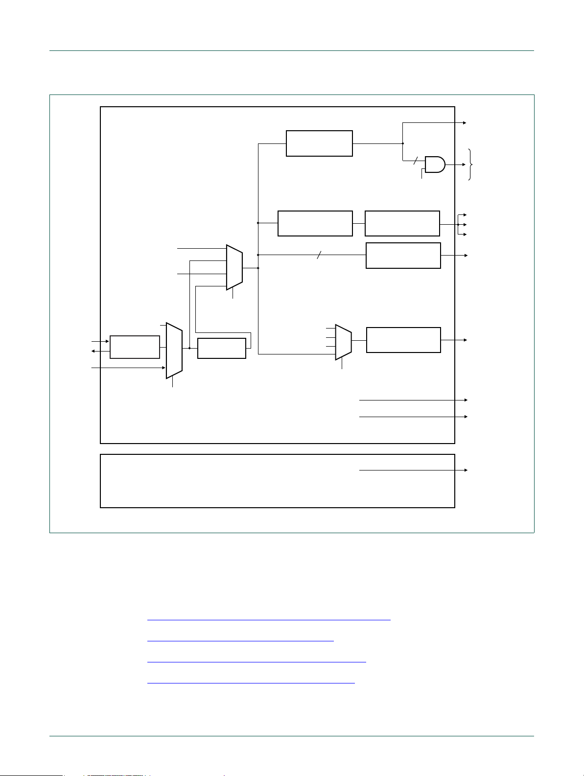
The system control block generates all clocks for the chip. Only the low-power oscillator
used for wake-up timing is controlled by the PMU. Except for the USART clock and the
clock to configure the glitch filters of the digital I/O pins, the clocks to the core and
peripherals run at the same frequency. The maximum system clock frequency is 30 MHz.
See Figure 5
.
Remark: The main clock frequency is limited to 100 MHz.
UM10800 All information provided in this document is subject to legal disclaimers. © NXP Semiconductors N.V. 2016. All rights reserved.
User manual Rev. 1.2 — 5 October 2016 29 of 487
Page 30
NXP Semiconductors
UM10800
Chapter 5: LPC82x System configuration (SYSCON)
XTALIN
XTALOUT
CLKIN
SYSCON
IRC oscillator
watchdog oscillator
IRC oscillator
SYSTEM
OSCILLATOR
SYSPLLCLKSEL
system PLL clock select
MAINCLKSEL
(main clock select)
SYSTEM PLL
main clock system clock
CLOCK DIVIDER
SYSAHBCLKDIV
CLOCK DIVIDER
UARTCLKDIV
7
IRC oscillator
system oscillator
watchdog oscillator
(CLKOUT clock select)
watchdog oscillator
IRC oscillator
SYSAHBCLKCTRL[1:19]
(system clock enable)
FRACTIONAL RATE
GENERATOR
CLOCK DIVIDER
IOCONCLKDIV
CLOCK DIVIDER
CLKOUTDIV
CLKOUTSEL
AHB clock 0
(core, system;
always-on)
19
memories
and peripherals,
peripheral clocks
USART0
USART1
USART2
IOCON
glitch filter
CLKOUT pin
WWDT
WKT
PMU
low-power oscillator
WKT
Fig 5. Clock generati on
5.5.2 Power control of analog components
The system control block controls the power to the analog components such as the
oscillators and PLL, the BOD, and the analog comparator. For details, see the following
registers:
Section 5.6.31 “
Section 5.6.3 “System PLL control register”
Section 5.6.6 “Watchdog oscillator control register”
Section 5.6.5 “System oscillator control register”
UM10800 All information provided in this document is subject to legal disclaimers. © NXP Semiconductors N.V. 2016. All rights reserved.
User manual Rev. 1.2 — 5 October 2016 30 of 487
Deep-sleep mode configuration register”
Page 31

NXP Semiconductors
5.5.3 Configuration of reduced power-modes
The system control block configures analog blocks that can remain running in the reduced
power modes (the BOD and the watchdog oscillator for safe operation) and enables
various interrupts to wake up the chip when the internal clocks are shut down in
Deep-sleep and Power-down modes. For details, see the following registers:
UM10800
Chapter 5: LPC82x System configuration (SYSCON)
Section 5.6.33 “
Power configuration register”
Section 5.6.30 “Start logic 1 interrupt wake-up enable register”
5.5.4 Reset and interrupt control
The peripheral reset control register in the system control register allows to assert and
release individual peripheral resets. See Table 23
.
Up to eight external pin interrupts can be assigned to any digital pin in the system control
block (see Section 5.6.28 “
Pin interrupt select registers”).
5.6 Register description
All system control block registers reside on word address boundaries. Details of the
registers appear in the description of each function.
Reset values describe the content of the registers after the bootloader has executed.
All address offsets not shown in Table 21
Table 21. Register overview: System configura t ion (base address 0x4004 8000)
Name Access Offset Description Reset value Reset
SYSMEMREMAP R/W 0x000 System memory remap 0x2 Table 22
PRESETCTRL R/W 0x004 Peripheral reset control 0x0001 FFFF Table 23
SYSPLLCTRL R/W 0x008 System PLL control 0 Table 24
SYSPLLST AT R 0x00C System PLL status 0 Table 25
- - 0x010 Reserved - -
- - 0x014 Reserved - SYSOSCCTRL R/W 0x020 System oscillator control 0x000 Table 26
WDTOSCCTRL R/W 0x024 Watchdog oscillator control 0x0A0 Table 27
IRCCTRL R/W 0x028 IRC control 0x080 Table 28
- - 0x02C Reserved - SYSRSTSTAT R/W 0x030 System reset status register 0 Table 29
SYSPLLCLKSEL R/W 0x040 System PLL clock source select 0 Table 30
SYSPLLCLKUEN R/W 0x044 System PLL clock source update enable 0 Table31
MAINCLKSEL R/W 0x070 Main clock source select 0 Table 32
MAINCLKUEN R/W 0x074 Main clock source update enable 0 Table33
SYSAHBCLKDIV R/W 0x078 System clock divider 1 T able34
SYSAHBCLKCTRL R/W 0x080 System clock control 0xDF Table 35
UARTCLKDIV R/W 0x094 USART clock divider 0 Table 36
UM10800 All information provided in this document is subject to legal disclaimers. © NXP Semiconductors N.V. 2016. All rights reserved.
User manual Rev. 1.2 — 5 October 2016 31 of 487
are reserved and should not be written to.
Reference
value
after boot
Page 32

NXP Semiconductors
UM10800
Chapter 5: LPC82x System configuration (SYSCON)
Table 21. Register overview: System configura t ion (base address 0x4004 8000) …continued
Name Access Offset Description Reset value Reset
value
after boot
- - 0x098 Reserved - -
- - 0x09C Reserved - -
- - 0x0A0 0x0BC
- - 0x0CC Reserved - -
CLKOUTSEL R/W 0x0E0 CLKOUT clock source select 0 Table 37
CLKOUTUEN R/W 0x0E4 CLKOUT clock source update enable 0 Table 38
CLKOUTDIV R/W 0x0E8 CLKOUT clock divider 0 Table 39
UARTFRGDIV R/W 0x0F0 USART1 to USART4 common fractional
UARTFRGMULT R/W 0x0F4 USART1 to USART4 common fractional
EXTTRACECMD R/W 0x0FC External trace buffer command register 0 Table 42
PIOPORCAP0 R 0x100 POR captured PIO status 0 user
- - 0x104 Reserved - -
IOCONCLKDIV6 R/W 0x134 Peripheral clock 6 to the IOCON block for
IOCONCLKDIV5 R/W 0x138 Peripheral clock 5 to the IOCON block for
IOCONCLKDIV4 R/W 0x13C Peripheral clock 4 to the IOCON block for
IOCONCLKDIV3 R/W 0x140 Peripheral clock 3 to the IOCON block for
IOCONCLKDIV2 R/W 0x144 Peripheral clock 2 to the IOCON block for
IOCONCLKDIV1 R/W 0x148 Peripheral clock 1 to the IOCON block for
IOCONCLKDIV0 R/W 0x14C Peripheral clock 0 to the IOCON block for
BODCTRL R/W 0x150 Brown-Out Detect 0 Table 45
SYSTCKCAL R/W 0x154 System tick counter calibration 0 Table 46
- R/W 0x168 Reserved - -
IRQLAT ENCY R/W 0x170 IQR delay. Allows trade-off between
NMISRC R/W 0x174 NMI Source Control 0 Table 48
PINTSEL0 R/W 0x178 GPIO Pin Interrupt Select register 0 0 Table 49
PINTSEL1 R/W 0x17C GPIO Pin Interrupt Select register 1 0 Table 49
PINTSEL2 R/W 0x180 GPIO Pin Interrupt Select register 2 0 Table 49
PINTSEL3 R/W 0x184 GPIO Pin Interrupt Select register 3 0 Table 49
PINTSEL4 R/W 0x188 GPIO Pin Interrupt Select register 4 0 Table 49
PINTSEL5 R/W 0x18C GPIO Pin Interrupt Select register 5 0 Table 49
PINTSEL6 R/W 0x190 GPIO Pin Interrupt Select register 6 0 Table 49
UM10800 All information provided in this document is subject to legal disclaimers. © NXP Semiconductors N.V. 2016. All rights reserved.
User manual Rev. 1.2 — 5 October 2016 32 of 487
Reserved - -
0 Table 40
generator divider value
0 Table 41
generator multiplier value
dependent
0 Table 44
programmable glitch filter
0 Table 44
programmable glitch filter
0 Table 44
programmable glitch filter
0 Table 44
programmable glitch filter
0 Table 44
programmable glitch filter
0 Table 44
programmable glitch filter
0 Table 44
programmable glitch filter
0x0000 0010 Table 47
interrupt latency and determinism.
Reference
Table 43
Page 33

NXP Semiconductors
UM10800
Chapter 5: LPC82x System configuration (SYSCON)
Table 21. Register overview: System configura t ion (base address 0x4004 8000) …continued
Name Access Offset Description Reset value Reset
value
after boot
PINTSEL7 R/W 0x194 GPIO Pin Interrupt Select register 7 0 Table 49
STARTERP0 R/W 0x204 Start logic 0 pin wake-up enable register 0 Table 50
STARTERP1 R/W 0x214 Start logic 1 interrupt wake-up enable
register
PDSLEEPCFG R/W 0x230 Power-down states in deep-sleep mode 0xFFFF Table 52
PDAWAKECFG R/W 0x234 Power-down states for wake-up from
deep-sleep
PDRUNCFG R/W 0x238 Power configuration register 0xEDF0 Table 54
DEVICE_ID R 0x3F8 Device ID part
0 Table 51
0xEDF0 Table 53
dependent
Reference
Table 55
5.6.1 System memory remap register
The system memory remap register selects whether the exception ve ctors are read from
boot ROM, flash, or SRAM. By default, the flash memory is mapped to address
0x0000 0000. When the MAP bits in the SYSMEMREMAP register are set to 0x0 or 0x1,
the boot ROM or RAM respectively are mapped to the bottom 512 bytes of the memory
map (addresses 0x0000 0000 to 0x0000 0200).
Table 22. System memory remap register (SYSMEMREMAP, address 0x4004 8000) bit
description
Bit Symbol Value Description Reset
value
1:0 MAP System memory remap. Value 0x3 is reserved. 0x2
0x0 Bootloader Mode. Interrupt vectors are re-mapped to Boot
ROM.
0x1 Use r RAM Mode. Interrupt vectors are re-mapped to Static
RAM.
0x2 Use r Flash Mode. Interrupt vectors are not re-mapped and
reside in Flash.
31:2 - - Reserved -
5.6.2 Peripheral reset control register
The PRESETCTRL register allows software to reset specific peripherals. A zero in any
assigned bit in this register resets the specified peripheral. A 1 clears the reset and allows
the peripheral to operate.
Table 23. Peripheral reset control register (PRESETCTRL, address 0x4004 8004) bit
description
Bit Symbol Value Description Reset
value
0 SPI0_RST_N SPI0 reset control 1
0 Assert the SPI0 reset.
1 Clear the SPI0 reset.
UM10800 All information provided in this document is subject to legal disclaimers. © NXP Semiconductors N.V. 2016. All rights reserved.
User manual Rev. 1.2 — 5 October 2016 33 of 487
Page 34

NXP Semiconductors
Table 23. Peripheral reset control register (PRESETCTRL, address 0x4004 8004) bit
Bit Symbol Value Description Reset
1 SPI1_RST_N SPI1 reset control 1
2 UARTFRG_RST_N USART fractional baud rate generator
3 UART0_RST_N USART0 reset control 1
4 UART1_RST_N USART1 reset control 1
5 UART2_RST_N USART2 reset control 1
6 I2C0_RST_N I2C0 reset control 1
7 MRT_RST_N Multi-rate timer (MRT) reset control 1
8 SCT_RST_N SCT reset control 1
9 WKT_RST_N Self-wake-up timer (WKT) reset control 1
10 GPIO_RST_N GPIO and GPIO pin interrupt reset control 1
11 FLASH_RST_N Flash controller reset control 1
12 ACMP_RST_N Analog comparator reset control 1
13 - - Reserved -
UM10800
Chapter 5: LPC82x System configuration (SYSCON)
description
value
0 Assert the SPI1 reset.
1 Clear the SPI1 reset.
1
(UARTFRG) reset control
0 Assert the UARTFRG reset.
1 Clear the UARTFRG reset.
0 Assert the USART0 reset.
1 Clear the USART0 reset.
0 Assert the USART reset.
1 Clear the USART1 reset.
0 Assert the USART2 reset.
1 Clear the USART2 reset.
0 Assert the I2C0 reset.
1 Clear the I2C0 reset.
0 Assert the MRT reset.
1 Clear the MRT reset.
0 Assert the SCT reset.
1 Clear the SCT reset.
0 Assert the WKT reset.
1 Clear the WKT reset.
0 Assert the GPIO reset.
1 Clear the GPIO reset.
0 Assert the flash controller reset.
1 Clear the flash controller reset.
0 Assert the analog comparator reset.
1 Clear the analog comparator controller reset.
UM10800 All information provided in this document is subject to legal disclaimers. © NXP Semiconductors N.V. 2016. All rights reserved.
User manual Rev. 1.2 — 5 October 2016 34 of 487
Page 35

NXP Semiconductors
Table 23. Peripheral reset control register (PRESETCTRL, address 0x4004 8004) bit
Bit Symbol Value Description Reset
14 I2C1_RST_N I2C1 reset control 1
15 I2C2_RST_N I2C2 reset control 1
16 I2C3_RST_N I2C3 reset control 1
23:17 - - Reserved 24 ADC_RST_N ADC reset control 1
28:25 - - Reserved 29 DMA_RST_N DMA reset control 1
31:30 - - Reserved -
UM10800
Chapter 5: LPC82x System configuration (SYSCON)
description
value
0 Assert the I2C1 reset.
1 Clear the I2C1 reset.
0 Assert the I2C2 reset.
1 Clear the I2C2 reset.
0 Assert the I2C3 reset.
1 Clear the I2C3 reset.
0 Assert the ADC reset.
1 Clear the ADC reset.
0 Assert the DMA reset.
1 Clear the DMA reset.
5.6.3 System PLL control register
This register connects and enables the system PLL and co nfigures the PLL m ultiplier and
divider values. The PLL accepts an input frequency from 10 MHz to 25 MHz from various
clock sources. The input frequency is multiplied to a higher frequency and then divided
down to provide the actual clock used by the CPU, peripherals, and memories. The PLL
can produce a clock up to the maximum allowed for the CPU.
Remark: The divider values for P and M must be selected so that the PLL output clock
frequency FCLKOUT is lower than 100 MHz.
Table 24. System PLL control register (SYSPLLCTRL, address 0x4004 8008) bit description
Bit Symbol Value Description Reset
4:0 M SEL Feedback divider value. The division value M is the
programmed MSEL value + 1.
00000: Division ratio M = 1
to
11111: Division ratio M = 32
value
0
UM10800 All information provided in this document is subject to legal disclaimers. © NXP Semiconductors N.V. 2016. All rights reserved.
User manual Rev. 1.2 — 5 October 2016 35 of 487
Page 36

NXP Semiconductors
UM10800
Chapter 5: LPC82x System configuration (SYSCON)
T able 24. System PLL control register (SYSPLLCTRL, address 0x4004 8008) bit description
Bit Symbol Value Description Reset
6:5 PSEL Post divider ratio P. The division ratio is 2 P. 0
0x0 P = 1
0x1 P = 2
0x2 P = 4
0x3 P = 8
31:7 - - Reserved. Do not write ones to reserved bits. -
5.6.4 System PLL status register
This register is a Read-only register and supplies the PLL lock status (see
Section 5.7.4.1
Table 25. System PLL status register (SYSPLLSTAT, address 0x4004 800C) bit description
Bit Symbol Value Description Reset
0 LOCK PLL lock status 0
31:1 - - Reserved -
).
0 PLL not locked
1 PLL locked
value
value
5.6.5 System oscillator control register
This register configures the frequency range for the system oscillator. The system
oscillator itself is powered on or off in the PDRUNCFG register. See Table 54
Table 26. System oscillator control register (SYSOSCCTRL, address 0x4004 8020) bit
description
Bit Symbol Value Description Reset
0 BYPASS Bypass system oscillator 0x0
0 Disabled. Oscillator is not bypassed.
1 Enabled. PLL input (sys_osc_clk) is fed directly
from the XTALIN pin bypassing the oscillator. Use
this mode when using an external clock source
instead of the crystal oscillator.
1 FREQRANGE Determines oscillator frequency range. 0x0
0 1 - 20 MHz frequency range.
1 15 - 25 MHz frequency range
31:2 - - Reserved 0x00
5.6.6 Watchdog oscillator control register
This register configures the watchdog oscillator. The oscillator consists of an analog and a
digital part. The analog part contains the oscillator function and generates an analog clock
(Fclkana). With the digital part, the analog output clock (Fclkana) can be divided to the
.
value
UM10800 All information provided in this document is subject to legal disclaimers. © NXP Semiconductors N.V. 2016. All rights reserved.
User manual Rev. 1.2 — 5 October 2016 36 of 487
Page 37

NXP Semiconductors
required output clock frequency wdt_osc_clk. The analog output freque ncy (Fclkana) can
be adjusted with the FREQSEL bits between 600 kHz and 4.6 MHz. With the digital part
Fclkana will be divided (divider ratios = 2, 4,...,64) to wdt_osc_clk using the DIVSEL bits.
The output clock frequency of the watchdog oscillator can be calculated as
wdt_osc_clk = Fclkana/(2 (1 + DIVSEL)) = 9.3 kHz to 2.3 MHz (nominal values).
Remark: Any setting of the FREQSEL bits will yield a Fclkana value within 40% of the
listed frequency value. The watchdog oscillator is the clock source with the lowest power
consumption. If accurate timing is required, use the IRC or system oscillator.
Remark: The frequency of the watchdog oscillator is undefined after reset. The watchdog
oscillator frequency must be programmed by writing to the WDTOSCCTRL register before
using the watchdog oscillator.
Table 27. Watchdog oscillator control register (WDTOSCCTRL, address 0x4004 8024) bit
Bit Symbol Value Description Reset
4:0 DIVSEL Select divider for Fclkana.
8:5 FREQSEL Select watchdog oscillator analog output frequen cy
31:9 - - Reserved 0x00
UM10800
Chapter 5: LPC82x System configuration (SYSCON)
description
value
0
wdt_osc_clk = Fclkana/ (2 (1 + DIVSEL))
00000: 2 (1 + DIVSEL) = 2
00001: 2 (1 + DIVSEL) = 4
to
11111: 2 (1 + DIVSEL) = 64
0x00
(Fclkana).
0x1 0.6 MHz
0x2 1.05 MHz
0x3 1.4 MHz
0x4 1.75 MHz
0x5 2.1 MHz
0x6 2.4 MHz
0x7 2.7 MHz
0x8 3.0 MHz
0x9 3.25 MHz
0xA 3.5 MHz
0xB 3.7 5 MH z
0xC 4.0 MHz
0xD 4.2 MHz
0xE 4.4 MHz
0xF 4.6 MHz
5.6.7 Internal resonant crystal control register
This register can be used to re-trim the on-chip 12 MHz oscillator. Note that the
factory-preset trim value is written to this register by the boot code on start-up.
UM10800 All information provided in this document is subject to legal disclaimers. © NXP Semiconductors N.V. 2016. All rights reserved.
User manual Rev. 1.2 — 5 October 2016 37 of 487
Page 38

NXP Semiconductors
Table 28. Internal resonant crystal control register (IRCCTRL, address 0x4004 8028) bit
Bit Symbol Description Reset valu e
7:0 TRIM Trim value 0x80, then flash will reprogram
31:8 - Reserved 0x00
UM10800
Chapter 5: LPC82x System configuration (SYSCON)
description
UM10800 All information provided in this document is subject to legal disclaimers. © NXP Semiconductors N.V. 2016. All rights reserved.
User manual Rev. 1.2 — 5 October 2016 38 of 487
Page 39

NXP Semiconductors
5.6.8 System reset status register
The SYSRSTSTAT register shows the source of the latest reset event. The bits are
cleared by writing a one to any of the bits. The POR event clears all other bits in this
register. If another reset signal - for example the external RESET
after the POR signal is negated, then its bit is set to detected. Write a one to clear the
reset.
UM10800
Chapter 5: LPC82x System configuration (SYSCON)
pin - remains asserted
The reset value given in Table 29
Table 29. System reset status register (SYSRSTSTAT, address 0x4004 8030) bit description
Bit Symbol Value Description Reset
0 POR POR reset status 0
0 No POR detected
1 POR detected. Writing a one clears this reset.
1 EXTRST Status of the external RESET
0 No reset event detect ed .
1 Reset detected. Writing a one clears this reset.
2 WDT Status of the Watchdog reset 0
0 No WDT reset detected
1 WDT reset detected. Writing a one clears this reset.
3 BOD Status of the Brown-out detect reset 0
0 No BOD reset detected
1 BOD reset detected. Writing a one clears this reset.
4 SYSRST Status of the software system reset 0
0 No System reset detected
1 System reset detected. Writing a one clears this reset.
31:5 - - Reserved -
applies to the POR reset.
value
pin. External reset status. 0
5.6.9 System PLL clock source select register
This register selects the clock source for the system PLL. The SYSPLLCLKUEN register
(see Section 5.6.10
T able 30. System PLL clock source select register (SYSPLLCLKSEL, address 0x4004 8040)
bit description
Bit Symbol Value Description Reset
1:0 SEL System PLL clock source 0
31:2 - - Reserved -
UM10800 All information provided in this document is subject to legal disclaimers. © NXP Semiconductors N.V. 2016. All rights reserved.
User manual Rev. 1.2 — 5 October 2016 39 of 487
) must be toggled from LOW to HIGH for the update to take effect.
value
0x0 IRC
0x1 Crystal Oscillator (SYSOSC)
0x2 Reserved.
0x3 CLKIN. External clock input.
Page 40

NXP Semiconductors
5.6.10 System PLL clock source update register
This register updates the clock source of the system PLL with the new input clock after the
SYSPLLCLKSEL register has been written to. In order for the update to take effect, first
write a zero to the SYSPLLUEN register and then write a one to SYSPLLUEN.
Table 31. System PLL clock source update enable register (SYSPLLCLKUEN, address
Bit Symbol Value Description Reset value
0 ENA Enable system PLL clock source update 0
31:1 - - Reserved -
5.6.11 Main clock source select register
This register selects the main system clock, which can be the system PLL (sys_pllclkout),
or the watchdog oscillator, or the IRC oscillator. The main system clock clocks the core,
the peripherals, and the memories.
UM10800
Chapter 5: LPC82x System configuration (SYSCON)
0x4004 8044) bit description
0 No change
1 Update clock source
Bit 0 of the MAINCLKUEN register (see Section 5.6.12
the update to take effect.
Table 32. Main clock source select register (MAINCL KSEL, address 0x4004 8070) bit
description
Bit Symbol Value Description Reset value
1:0 SEL Clock source for main clock 0
0x0 IRC Oscillator
0x1 PLL input
0x2 Watchdog oscillator
0x3 PLL output
31:2 - - Reserved -
5.6.12 Main clock source update enable register
This register updates the clock source of the main clock with the new input clock after the
MAINCLKSEL register has been written to. In order for the update to take effect, first write
a zero to bit 0 of this register, then write a one.
Table 33. Main clock source update enable register (MAINCLKUEN, address 0x4004 8074)
bit description
Bit Symbol Value Description Reset value
0 ENA Enable main clock source update 0
0 No change
1 Update clock source
31:1 - - Reserved -
) must be toggled from 0 to 1 for
UM10800 All information provided in this document is subject to legal disclaimers. © NXP Semiconductors N.V. 2016. All rights reserved.
User manual Rev. 1.2 — 5 October 2016 40 of 487
Page 41

NXP Semiconductors
5.6.13 System clock divider register
This register controls how the main clock is divided to provide the system clock to the
core, memories, and the peripherals. The system clock can be shut down completely by
setting the DIV field to zero.
Table 34. System clock divider register (SYSAHBCLKDIV, address 0x4004 8078) bit
Bit Symbol Description Reset
7:0 DIV System AHB clock divider values
31:8 - Reserved -
5.6.14 System clock control register
The SYSAHBCLKCTRL register enables the clocks to individual system and peripheral
blocks. The system clock (bit 0) provides the clock for the AHB, the APB br idge , th e ARM
Cortex-M0+, the SYSCON block, and the PMU. This clock cannot be disabled.
Table 35. System clock control register (SYSAHBCLKCTRL, address 0x4004 8080) bit
Bit Symbol Value Description Reset
0 SYS Enables the clock for the AHB, the APB bridge, the
1 ROM Enables clock for ROM. 1
2 RAM0_1 Enables clock for SRAM0 and SRAM1. 1
3 FLASHREG Enables clock for flash register interface. 1
4 FLASH Enables clock for flash. 1
5 I2C0 Enables clock for I2C0. 0
6 GPIO Enables clock for GPIO port registers and GPIO pin
UM10800
Chapter 5: LPC82x System configuration (SYSCON)
description
value
0x01
0: System clock disabled.
1: Divide by 1.
to
255: Divide by 255.
description
value
1
Cortex-M0+ core clocks, SYSCON, and the PMU.
This bit is read only and always reads as 1.
0 Disable
1 Enable
0 Disable
1 Enable
0 Disable
1 Enable
0 Disable
1 Enable
0 Disable
1 Enable
1
interrupt registers.
0 Disable
1 Enable
UM10800 All information provided in this document is subject to legal disclaimers. © NXP Semiconductors N.V. 2016. All rights reserved.
User manual Rev. 1.2 — 5 October 2016 41 of 487
Page 42

NXP Semiconductors
UM10800
Chapter 5: LPC82x System configuration (SYSCON)
Table 35. System clock control register (SYSAHBCLKCTRL, address 0x4004 8080) bit
description
Bit Symbol Value Description Reset
7 SWM Enables clock for switch matrix. 1
8 SCT Enables clock for state configurable timer
9 WKT Enables clock for self-wake-up timer. 0
10 MRT Enables clock for multi-rate timer.
11 SPI0 Enables clock for SPI0. 0
12 SPI1 Enables clock for SPI1.
13 CRC Enables clock for CRC. 0
14 UART0 Enabl es clock for USART0. 0
15 UART1 Enabl es clock for USART1. 0
16 UART2 Enabl es clock for USART2. 0
17 WWDT Enables clock for WWDT. 0
18 IOCON Enables clock for IOCON block. 0
19 ACMP Enables clock to analog comparator. 0
UM10800 All information provided in this document is subject to legal disclaimers. © NXP Semiconductors N.V. 2016. All rights reserved.
User manual Rev. 1.2 — 5 October 2016 42 of 487
…continued
value
0 Disable
1 Enable
0
SCTimer/PWM.
0 Disable
1 Enable
0 Disable
1 Enable
0 Disable
1 Enable
0 Disable
1 Enable
0 Disable
1 Enable
0 Disable
1 Enable
0 Disable
1 Enable
0 Disable
1 Enable
0 Disable
1 Enable
0 Disable
1 Enable
0 Disable
1 Enable
0 Disable
1 Enable
Page 43

NXP Semiconductors
Table 35. System clock control register (SYSAHBCLKCTRL, address 0x4004 8080) bit
Bit Symbol Value Description Reset
20 - - Reserved 21 I2C1 Enables clock to I2C1. 0
22 I2C2 Enables clock to I2C2. 0
23 I2C3 Enables clock to I2C3. 0
24 ADC Enables clock to ADC. 0
25 - - Reserved 26 MTB Enables clock to micro-trace buffer control registers.
28:27 - - Reserved 29 DMA Enables clock to DMA. 0
31:30 - - Reserved -
description
UM10800
Chapter 5: LPC82x System configuration (SYSCON)
…continued
value
0 Disable
1 Enable
0 Disable
1 Enable
0 Disable
1 Enable
0 Disable
1 Enable
0
Turn on this clock when using the micro-trace buffer
for debug purposes.
0 Disable
1 Enable
0 Disable
1 Enable
5.6.15 USART clock divider register
This register configures the clock for the fractional baud rate generator and all USARTs.
The UART clock can be disabled by setting the DIV field to zero (this is the default
setting).
T able 36. USART clock divider register (UARTCLKDIV, address 0x4004 8094) bit description
Bit Symbol Description Reset
value
7:0 DIV USART fractional baud rate generator clock divider values.
0: Clock disabled.
1: Divide by 1.
to
255: Divide by 255.
31:8 - Reserved -
UM10800 All information provided in this document is subject to legal disclaimers. © NXP Semiconductors N.V. 2016. All rights reserved.
User manual Rev. 1.2 — 5 October 2016 43 of 487
0
Page 44

NXP Semiconductors
5.6.16 CLKOUT clock source select register
This register selects the signal visible on the CLKOUT pin. Any oscillator or the main clock
can be selected.
UM10800
Chapter 5: LPC82x System configuration (SYSCON)
Bit 0 of the CLKOUTUEN register (see Section 5.6.17
) must be toggled from 0 to 1 for the
update to take effect.
Table 37. CLKOUT clock source select register (CLKOUTSEL, address 0x4004 80E0) bit
description
Bit Symbol Value Description Reset
1:0 SEL CLKOUT clock source 0
0x0 IRC oscillator
0x1 Crystal oscillator (SYSOSC)
0x2 Watchdog oscillator
0x3 Main clock
31:2 - - Reserved 0
5.6.17 CLKOUT clock source update enable register
This register updates the clock source of the CLKOUT pin with the new clock after the
CLKOUTSEL register has been written to. In order for the update to t ake effect at the input
of the CLKOUT pin, first write a zero to bit 0 of this register, then write a one.
Table 38. CLKOUT clock source update enable register (CLKOUTUEN, address 0x40 04
80E4) bit description
Bit Symbol Value Description Reset value
0 ENA Enable CLKOUT clock source update 0
0 No change
1 Update clock source
31:1 - - Reserved -
value
5.6.18 CLKOUT clock divider register
This register determines the divider value for the signal on the CLKOUT pin.
Table 39. CLKOUT clock divider register s (CLKOUTDIV, address 0x4004 80E8) bit
description
Bit Symbol Description Reset
value
7:0 DIV CLKOUT clock divider values
0: Disable CLKOUT clock divider.
1: Divide by 1.
to
255: Divide by 255.
31:8 - Reserved -
0
5.6.19 USART fractional generator divider value register
All USART peripherals share a common clock U_PCLK, which can be adjusted by a
fractional divider:
UM10800 All information provided in this document is subject to legal disclaimers. © NXP Semiconductors N.V. 2016. All rights reserved.
User manual Rev. 1.2 — 5 October 2016 44 of 487
Page 45

NXP Semiconductors
U_PCLK = UARTCLKDIV/(1 + MULT/DIV).
UARTCLKDIV is the USART clock configured in the UARTCLKDIV register.
The fractional portion (1 + MULT/DIV) is determined by the two USART fractional divider
registers in the SYSCON block:
1. The DIV value programmed in this register is the denominator of the divider used by
2. The MULT value of the fractional divider is programmed in the UARTFRGMULT
Remark: To use of the fractional baud rate generator, you must write 0xFF to this r egister
to yield a denominator value of 256. All other values are not supported.
See also:
UM10800
Chapter 5: LPC82x System configuration (SYSCON)
the fractional rate generator to create the fractional component of U_PCLK.
register. See Table 41
.
Section 13.3.1 “
Configure the USART clock and baud rate”
Section 13.7.1 “Clocking and baud rates”
T able 40. USART fractional generator divider value register (UARTFRGDIV, address 0x4004
80F0) bit description
Bit Symbol Description Reset
7:0 DIV Denominator of the fractional divider. DIV is equal to the programmed
value +1. Always set to 0xFF to use with the fractional baud rate
generator.
31:8 - Reserved -
5.6.20 USART fractional generator multiplier value register
All USART peripherals share a common clock U_PCLK, which can be adjusted by a
fractional divider:
U_PCLK = UARTCLKDIV/(1 + MULT/DIV).
UARTCLKDIV is the USART clock configured in the UARTCLKDIV register.
The fractional portion (1 + MULT/DIV) is determined by the two USART fractional divider
registers in the SYSCON block:
value
0
1. The DIV denominator of the fractional divider value is programmed in the
UARTFRGDIV register. See Table 40
.
2. The MULT value programmed in this register is the numerator of th e fractiona l divider
value used by the fractional rate generator to create the fractional component to the
baud rate.
See also:
Section 13.3.1 “
Configure the USART clock and baud rate”
Section 13.7.1 “Clocking and baud rates”
UM10800 All information provided in this document is subject to legal disclaimers. © NXP Semiconductors N.V. 2016. All rights reserved.
User manual Rev. 1.2 — 5 October 2016 45 of 487
Page 46

NXP Semiconductors
T able 41. USART fractional generator multiplier value register (UARTFRGMULT, address
Bit Symbol Description Reset
7:0 MUL T Numerator of the fractional divider. MULT is equal to the programmed
31:8 - Reserved -
5.6.21 External trace buffer command register
This register works in conjunction with the MTB master register to start and stop tracing.
Also see Section 31.5.4
Table 42. External trace buffer command register (EXT TRACECMD, address 0x4004 80FC)
Bit Symbol Description Reset
0 START Trace start command. Writing a one to this bit sets the TST AR T signal
1 STOP Trace stop command. Writing a one to this bit sets the TSTOP signal
31:2 - Reserved 0
UM10800
Chapter 5: LPC82x System configuration (SYSCON)
0x4004 80F4) bit description
value
0
value.
.
bit description
value
0
to the MTB to HIGH and starts tracing if the TSTARTEN bit in the
MTB master register is set to one as well.
0
in the MTB to HIGH and stops tracing if the TSTOPEN bit in the MTB
master register is set to one as well.
5.6.22 POR captured PIO status register 0
The PIOPORCAP0 register captures the state of GPIO port 0 at power-on-r eset. Each bit
represents the reset state of one GPIO pin. This register is a read- on ly status register.
Table 43. POR captured PIO status register 0 (PIOPORCAP0, address 0x400 4 8100) bit
description
Bit Symbol Description Reset value
17:0 PIOSTAT State of PIO0_17 through PIO0_0 at power-on reset Implementation
31:18 - Reserved. -
5.6.23 IOCON glitch filter clock divider registers 6 to 0
These registers individually configure the seven peripheral input clocks
(IOCONFILTR_PCLK) to the IOCON programmable glitch filter. The clocks can be shut
down by setting the DIV bits to 0x0.
dependent
UM10800 All information provided in this document is subject to legal disclaimers. © NXP Semiconductors N.V. 2016. All rights reserved.
User manual Rev. 1.2 — 5 October 2016 46 of 487
Page 47

NXP Semiconductors
Table 44. IOCON glitch filter clock divider registers 6 to 0 (IOCONCLKDIV[6:0], ad dress
Bit Symbol Description Reset value
7:0 DIV IOCON glitch filter clock divider values
31:8 - Reserved 0x00
5.6.24 BOD control register
The BOD control register selects four separate threshold values for sending a BOD
interrupt to the NVIC and for forced reset. Reset and interrupt threshold values listed in
Table 45
Both the BOD interrupt and the BOD reset, depending on the value of bit BODRSTENA in
this register, can wake-up the chip from Sleep, Deep-sleep, and Power-down modes.
UM10800
Chapter 5: LPC82x System configuration (SYSCON)
0x4004 8134 (IOCONCLKDIV6) to 0x004 814C (IOCONFILT CLKDIV0)) bit
description
0
0: Disable IOCONFILTR_PCLK.
1: Divide by 1.
to
255: Divide by 255.
are typical values.
See the LPC800 data sheet for the BOD reset and interrupt levels.
Table 45. BOD control register (BODCTRL, address 0x4004 8150) bit description
Bit Symbol Value Description Reset
1:0 BODRSTLEV BOD reset level 0
0x0 Reserved.
0x1 Level 1.
0x2 Level 2.
0x3 Level 3.
3:2 BODINTVAL BOD interrupt level 0
0x0 Reserved
0x1 Level 1.
0x2 Level 2.
0x3 Level 3.
4 BODRSTENA BOD reset enable 0
0 Disable reset function.
1 Enable reset function.
31:5 - - Reserved 0x00
5.6.25 System tick counter calibration register
value
This register determines the value of the SYST_CALIB register.
Table 46. System tick timer calibration register (SYSTCKCAL, address 0x4004 8154) bit
description
Bit Symbol Description Reset
value
25:0 CAL System tick timer calibration value 0
31:26 - Reserved -
UM10800 All information provided in this document is subject to legal disclaimers. © NXP Semiconductors N.V. 2016. All rights reserved.
User manual Rev. 1.2 — 5 October 2016 47 of 487
Page 48

NXP Semiconductors
5.6.26 IRQ latency register
The IRQLA TENCY r egister is an eight-b it register which specifies the minimum number of
cycles (0-255) permitted for the system to respond to an interrupt request. The intent of
this register is to allow the user to select a trade-off between interrupt response time and
determinism.
Setting this parameter to a very low value (e.g. zero) will guarantee the best possible
interrupt performance but will also introduce a significant degree of uncertainty and jitter.
Requiring the system to always take a larger number of cycles (whethe r it need s it o r not)
will reduce the amount of uncertainty but may not necessarily eliminate it.
Theoretically, the ARM Cortex-M0+ core should always be able to service an interrupt
request within 15 cycles. However, system factors external to the cpu, such as bus
latencies or peripheral response times, can increase the time required to complete a
previous instruction before an interrupt can be serviced. Therefore, accurately specifying
a minimum number of cycles that will ensure determinism will depend on the application.
The default setting for this register is 0x010.
Table 47. IRQ latency register (IRQLATENCY, address 0x4004 8170) bit description
Bit Symbol Description Reset
7:0 LATENCY 8-bit latency value 0x010
31:8 - Reserved -
UM10800
Chapter 5: LPC82x System configuration (SYSCON)
value
5.6.27 NMI source selection register
The NMI source selection register selects a peripheral interrupt as source for the NMI
interrupt of the ARM Cortex-M0+ core. For a list of all peripheral interrupts and their IRQ
numbers see Table 5
Remark: When you want to change the interr upt source for the NMI, you must first disable
the NMI source by setting bit 31 in this register to 0. Then change the source by updating
the IRQN bits and re-enable the NMI source by setting bit 31 to 1.
Table 48. NMI source selectio n register (NMISRC, address 0x4004 8174) bit description
Bit Symbol Description Reset
4:0 IRQN The IRQ number of the interrupt that acts as the Non-Maskable Interrupt
30:5 - Reserved 31 NMIEN Write a 1 to this bit to enable the Non-Maskable Interrupt (NMI) source
Remark: If the NMISRC register is used to select an interrupt as the source of
Non-Maskable interrupts, and the selected interrupt is enabled, one interrupt request can
result in both a Non-Maskable and a normal interrupt. This can be avoided by disabling
the normal interrupt in the NVIC.
. For a description of the NMI functionality, see Section 4.3.2.
(NMI) if bit 31 is 1. See Table 5
IRQ numbers.
selected by bits 4:0.
value
0
for the list of interrupt sources and their
0
UM10800 All information provided in this document is subject to legal disclaimers. © NXP Semiconductors N.V. 2016. All rights reserved.
User manual Rev. 1.2 — 5 October 2016 48 of 487
Page 49

NXP Semiconductors
5.6.28 Pin interrupt select registers
Each of these 8 registers selects one pin from all digital pins as the source of a pin
interrupt or as the input to the pattern match e ngine. To select a pin for any of the eight pin
interrupts or pattern match en gine inputs, write the GPIO port pin number as 0 to 28 for
pins PIO0_0 to PIO0_28 to the INTPIN bits. For example, setting INTPIN to 0x5 in
PINTSEL0 selects pin PIO0_5 for pin interrupt 0.
Remark: The GPIO port pin number serves to identify the pin to the PINTSEL register.
Any digital input function, including GPIO, can be assigned to this pin through the switch
matrix.
Each of the 8 pin interrupts must be enabled in the NVIC using interrupt slots # 24 to 31
(see Table 5
To use the selected pins for pin interrupts or the pattern match engine, see Section 10.5.2
“Pattern match engine”.
Table 49. Pin interrupt select registe rs (PINTSEL[0:7], address 0x4004 8178 (PINTSEL0) to
Bit Symbol Description Reset
5:0 INTPIN Pin number select for pin interrupt or pattern match engine input.
31:6 - Reserved -
UM10800
Chapter 5: LPC82x System configuration (SYSCON)
).
0x4004 8194 (PINTSEL7)) bit description
value
0
(PIO0_0 to PIO0_28 correspond to numbers 0 to 28).
5.6.29 Start logic 0 pin wake-up enable register
The STARTERP0 register enables the selected pin interrupts for wake-up from
deep-sleep mode and power-down modes.
Remark: Also enable the corresponding interrupts in the NVIC. See Table 5 “Connection
of interrupt sources to the NVIC”.
T able 50. Start logic 0 pin wake-up enable register 0 (STARTERP0, address 0x4004 8204) bit
description
Bit Symbol Value Description Reset
0 PINT0 GPIO pin interrupt 0 wake-up 0
0 Disabled
1 Enabled
1 PINT1 GPIO pin interrupt 1 wake-up 0
0 Disabled
1 Enabled
2 PINT2 GPIO pin interrupt 2 wake-up 0
0 Disabled
1 Enabled
3 PINT3 GPIO pin interrupt 3 wake-up 0
0 Disabled
1 Enabled
value
UM10800 All information provided in this document is subject to legal disclaimers. © NXP Semiconductors N.V. 2016. All rights reserved.
User manual Rev. 1.2 — 5 October 2016 49 of 487
Page 50

NXP Semiconductors
T able 50. Start logic 0 pin wake-up enable register 0 (STARTERP0, address 0x4004 8204) bit
Bit Symbol Value Description Reset
4 PINT4 GPIO pin interrupt 4 wake-up 0
5 PINT5 GPIO pin interrupt 5 wake-up 0
6 PINT6 GPIO pin interrupt 6 wake-up 0
7 PINT7 GPIO pin interrupt 7 wake-up 0
31:8 - Reserved -
description
UM10800
Chapter 5: LPC82x System configuration (SYSCON)
…continued
value
0 Disabled
1 Enabled
0 Disabled
1 Enabled
0 Disabled
1 Enabled
0 Disabled
1 Enabled
5.6.30 Start logic 1 interrupt wake-up enable register
This register selects which interrupts wake up the part from deep-sleep and power-down
modes.
Remark: Also enable the corresponding interrupts in the NVIC. See Table 5 “Connection
of interrupt sources to the NVIC”.
Table 51. Start logic 1 interrupt wake-up enable register (STARTERP1, address
0x4004 8214) bit description
Bit Symbol Value Description Reset
0 SPI0 SPI0 interrupt wake-up 0
0 Disabled
1 Enabled
1 SPI1 SPI1 interrupt wake-up 0
0 Disabled
1 Enabled
2 - Reserved 3 USART0 USART0 interrupt wake-up. Configure USART
in synchronous slave mode.
0 Disabled
1 Enabled
4 USART1 USART1 interrupt wake-up. Configure USART
in synchronous slave mode.
0 Disabled
1 Enabled
value
0
0
UM10800 All information provided in this document is subject to legal disclaimers. © NXP Semiconductors N.V. 2016. All rights reserved.
User manual Rev. 1.2 — 5 October 2016 50 of 487
Page 51

NXP Semiconductors
Table 51. Start logic 1 interrupt wake-up enable register (STARTERP1, address
Bit Symbol Value Description Reset
5 USART2 USART2 interrupt wake-up. Configure USART
6 - Reserved 7 I2C1 I2C1 interrupt wake-up. 0
8 I2C0 I2C0 interrupt wake-up. 0
11:9 - Reserved 12 WWDT WWDT interrupt wake-up 0
13 BOD BOD interrupt wake-up 0
14 - Reserved 15 WKT Self-wake-up timer interrupt wake-up 0
20:16 - Reserved. 21 I2C2 I2C2 interrupt wake-up. 0
22 I2C3 I2C3 interrupt wake-up. 0
31:23 - Reserved. -
Chapter 5: LPC82x System configuration (SYSCON)
0x4004 8214) bit description
in synchronous slave mode.
0 Disabled
1 Enabled
0 Disabled
1 Enabled
0 Disabled
1 Enabled
0 Disabled
1 Enabled
0 Disabled
1 Enabled
0 Disabled
1 Enabled
0 Disabled
1 Enabled
0 Disabled
1 Enabled
UM10800
…continued
value
0
5.6.31 Deep-sleep mode configuration register
The bits in this register (BOD_PD and WDTOSC_OD) can be programmed to control
aspects of Deep-sleep and Power-down modes. The bits are loaded into corresponding
bits of the PDRUNCFG register when Deep-sleep mode or Power-down mode is entered.
Remark: Hardware forces the analog blocks to be powered down in Deep-sleep and
Power-down modes. An exception are the BOD and watchdog oscillator, which can be
configured to remain running through this register. The WDTOSC_PD value written to the
PDSLEEPCFG register is overwritten if the LOCK bit in the WWDT MOD register (see
Table 253
UM10800 All information provided in this document is subject to legal disclaimers. © NXP Semiconductors N.V. 2016. All rights reserved.
User manual Rev. 1.2 — 5 October 2016 51 of 487
) is set. See Section 17.5.3 for details.
Page 52

NXP Semiconductors
Table 52. Deep-sleep configuration register (PDSLEEPCFG, address 0x4004 8230) bit
Bit Symbol Value Description Reset value
2:0 - Reserved. 0b111
3 BOD_PD BOD power-down control for Deep-sleep and
5:4 - Reserved. 1 1
6 WDTOSC_PD Watchdog oscillator power-down control for
15:7 - Reserved 0b111111111
31:16 - - Reserved 0
UM10800
Chapter 5: LPC82x System configuration (SYSCON)
description
1
Power-down mode
0 Powered
1 Powered down
1
Deep-sleep and Power-down mode. Changing
this bit to powered-down has no effect when the
LOCK bit in the WWDT MOD register is set. In
this case, the watchdog oscillator is always
running.
0 Powered
1 Powered down
5.6.32 Wake-up configuration register
This register controls the power configuration of the device when waking up from
Deep-sleep or Power-down mode.
Table 53. Wake-up configuration register (PDAWAKECFG, address 0x4004 8234) bit
description
Bit Symbol Value Description Reset value
0 IRCOUT_PD IRC oscillator output wake-up configuration 0
0 Powered
1 Powered down
1 IRC_PD IRC oscillator power-down wake-up configuration 0
0 Powered
1 Powered down
2 FLASH_PD Flash wake-up configuration 0
0 Powered
1 Powered down
3 BOD_PD BOD wake-up configuration 0
0 Powered
1 Powered down
4 ADC_PD ADC wake-up configuration 1
0 Powered
1 Powered down
5 SYSOSC_PD Crystal oscillator wake-up configuration 1
0 Powered
1 Powered down
UM10800 All information provided in this document is subject to legal disclaimers. © NXP Semiconductors N.V. 2016. All rights reserved.
User manual Rev. 1.2 — 5 October 2016 52 of 487
Page 53

NXP Semiconductors
Table 53. Wake-up configuration register (PDAWAKECFG, address 0x4004 8234) bit
Bit Symbol Value Description Reset value
6 WDTOSC_PD Watchdog oscillator wake-up configuration.
7 SYSPLL_PD System PLL wake-up configuration 1
11:8 - Reserved. Always write these bits as 0b1101 0b1101
14:12 - Reserved. Always write these bits as 0b110 0b110
15 ACMP Analog comparator wake-up configuration 1
31:16 - - Reserved 0
description
UM10800
Chapter 5: LPC82x System configuration (SYSCON)
…continued
1
Changing this bit to powered-down has no effect
when the LOCK bit in the WWDT MOD register is
set. In this case, the watchdog oscillator is always
running.
0 Powered
1 Powered down
0 Powered
1 Powered down
0 Powered
1 Powered down
5.6.33 Power configuration register
The PDRUNCFG register controls the power to the various analog blocks. This register
can be written to at any time while the chip is running, and a write will take effect
immediately with the exception of the power-down signal to the IRC.
To avoid glitches when powering down the IRC, the IRC clock is automatically switched
off at a clean point. Therefore, for the IRC a delay is possible before the powe r-down st ate
takes effect.
The system oscillator requires typically 500 μs to start up after the SYSOSC_PD bit has
been changed from 1 to 0. There is no hardware flag to monitor the state of the system
oscillator. Therefore, add a software delay of about 500 μs before using the system
oscillator after power-up.
Table 54. Power configuration register (PDRUNCFG, address 0x4004 8238) bit description
Bit Symbol Value Description Reset value
0 IRCOUT_PD IRC oscillator output power 0
0 Powered
1 Powered down
1 IRC_PD IRC oscillator power down 0
0 Powered
1 Powered down
2 FLASH_PD Flash power down 0
0 Powered
1 Powered down
UM10800 All information provided in this document is subject to legal disclaimers. © NXP Semiconductors N.V. 2016. All rights reserved.
User manual Rev. 1.2 — 5 October 2016 53 of 487
Page 54

NXP Semiconductors
UM10800
Chapter 5: LPC82x System configuration (SYSCON)
Table 54. Power configuration register (PDRUNCFG, address 0x4004 8238) bit description
Bit Symbol Value Description Reset value
3 BOD_PD BOD power down 0
0 Powered
1 Powered down
4 ADC_PD ADC wake -up configuration 1
0 Powered
1 Powered down
5 SYSOSC_PD Crystal oscillator power down. After power-up,
add a software delay of approximately 500 μs
before using.
0 Powered
1 Powered down
6 WDTOSC_PD Watchdog oscillator power down. Changing
this bit to powered-down has no effect when
the LOCK bit in the WWDT MOD register is
set. In this case, the watchdog oscillator is
always running.
0 Powered
1 Powered down
7 SYSPLL_PD System PLL power down 1
0 Powered
1 Powered down
1 1:8 - Reserved. Always write these bits as 0b1101 0b1101
14:12 - Reserved. Always write these bits as 0b110 0b110
15 ACMP Analog comparator power down 1
0 Powered
1 Powered down
31:16 - - Reserved 0
1
1
5.6.34 Device ID register
This device ID register is a read-only register and contains the part ID for each part. This
register is also read by the ISP/IAP commands (see Table 324
Table 55. Device ID register (DEVICE_ID, address 0x4004 83F8) bit description
Bit Symbol Description Reset value
31:0 DEVICEID 0x0000 8241 = LPC824M201JHI33
0x0000 8221 = LPC822M101JHI33
0x0000 8242 = LPC824M201JDH20
0x0000 8222 = LPC822M101JDH20
UM10800 All information provided in this document is subject to legal disclaimers. © NXP Semiconductors N.V. 2016. All rights reserved.
User manual Rev. 1.2 — 5 October 2016 54 of 487
).
part-dependent
Page 55

NXP Semiconductors
5.7 Functional description
5.7.1 Reset
Reset has the following sources: the RESET pin, Watchdog Reset, Power-On Reset
(POR), and Brown Out Detect (BOD). In addition, there is an ARM software reset.
UM10800
Chapter 5: LPC82x System configuration (SYSCON)
The RESET
the operating voltage attains a usable level, starts the IRC causing reset to remain
asserted until the external Reset is de-asserted, the oscillator is running, and the flash
controller has completed its initialization.
On the assertion of any reset source (ARM core software reset, POR, BOD reset, External
reset, and Watchdog reset), the following processes are initiated:
1. The IRC starts up. After the IRC-start-up time (maximum of 6 s on power-up), the
IRC provides a stable clock output.
2. The flash is powered up. This takes approximately 100 s. Then the flash initialization
sequence is started, which takes about 250 cycles.
3. The boot code in the ROM starts. The boot code performs the boot tasks and may
jump to the flash.
When the internal Reset is removed, the processor begins executing at address 0, which
is initially the Reset vector mapped from the boot block. At that point, all of the processor
and peripheral registers have been initialized to predetermined values.
pin is a Schmitt trigger input pin. Assertion of chip Reset by any source, once
5.7.2 Start-up behavior
See Figure 6 for the start-up timing after reset. The IRC is the default clock at Reset and
provides a clean system clock shortly after the supply volt age reaches the thresh old value
of 1.8 V.
UM10800 All information provided in this document is subject to legal disclaimers. © NXP Semiconductors N.V. 2016. All rights reserved.
User manual Rev. 1.2 — 5 October 2016 55 of 487
Page 56

NXP Semiconductors
IRC status
internal reset
V
DD
valid threshold
= 1.8V
GND
UM10800
Chapter 5: LPC82x System configuration (SYSCON)
IRC
starts
80 µs 101 µs
supply ramp-up
time
processor status
Fig 6. Start-up timing
5.7.3 Brown-out detection
boot time
55 µs
user code starts
user code
boot code
execution
finishes;
The brown-out detection circuit includes up to three levels for monitoring the voltage on
the V
pin. If this voltage falls below one of the selected levels, the BOD asserts an
DD
interrupt signal to the NVIC or issues a reset, depending on the value of the BODRSTENA
bit in the BOD control register (Table 45
).
The interrupt signal can be enabled for interrupt in the Interrupt Enable Register in the
NVIC (see Table 6
) in order to cause a CPU interrupt; if not, software can monitor the
signal by reading a dedicated status register.
If the BOD interrupt is enabled in the STARTERP1 register (see Table 51
) and in the
NVIC, the BOD interrupt can wake up the chip from Deep-sleep and power-do wn mode .
If the BOD reset is enabled, the forced BOD re set can wake up the chip from Deep-sleep
or Power-down mode.
5.7.4 System PLL functional description
The LPC82X uses the system PLL to create the clocks for the core and peripherals.
UM10800 All information provided in this document is subject to legal disclaimers. © NXP Semiconductors N.V. 2016. All rights reserved.
User manual Rev. 1.2 — 5 October 2016 56 of 487
Page 57

NXP Semiconductors
irc_osc_clk
sys_osc_clk
CLKIN
SYSPLLCLKSEL
Fig 7. System PLL block diagram
FCLKIN
PFD
LOCK
DETECT
analog section
pd
cd
/M
5
MSEL<4:0>
UM10800
Chapter 5: LPC82x System configuration (SYSCON)
FCCO
PSEL<1:0>
pd
LOCK
pd
2
cd
/2P
FCLKOUT
The block diagram of this PLL is shown in Figure 7. The input frequency range is 10 MHz
to 25 MHz. The input clock is fed directly to the Phase-Freq ue n cy Det ec to r (PF D). This
block compares the phase and frequency of its inputs, and generates a control signal
when phase and/ or frequency do not match. The loop filter filters these control signals
and drives the current controlled oscillator (CCO), which generates the main clock and
optionally two additional phases. The CCO frequency range is 156 MHz to 320 MHz.
These clocks are either divided by 2xP by the programmable post divider to create the
output clocks, or are sent directly to the outputs. The main output clock is then divided by
M by the programmable feedback divider to generate the feedback clock. The output
signal of the phase-frequency detector is also monitored by the lock detector, to signal
when the PLL has locked on to the input clock.
Remark: The divider values for P and M must be selected so that the PLL output clock
frequency FCLKOUT is lower than 100 MHz because the main clock is limited to a
maximum frequency of 100 MHz
5.7.4.1 Lock detector
The lock detector measures the phase difference between the rising edges of the input
and feedback clocks. Only when this difference is smaller than the so called “lock
criterion” for more than eight consecutive input clock periods, the lock output switches
from low to high. A single too large phase difference immediately resets the counter and
causes the lock signal to drop (if it was high). Requiring eig h t phase me asurements in a
row to be below a certain figure ensures that the lock detector will not indicate lock until
both the phase and frequency of the input and feedback clocks are very well aligned. This
effectively prevents false lock indications, and thus ensures a glitch free lock signal.
5.7.4.2 Power-down control
To reduce the power consumption when the PLL clock is not needed, a PLL Power-down
mode has been incorporated. This mode is enabled b y settin g th e SYSPLL_PD bit to on e
in the Power-down configuration register (Table 54
UM10800 All information provided in this document is subject to legal disclaimers. © NXP Semiconductors N.V. 2016. All rights reserved.
User manual Rev. 1.2 — 5 October 2016 57 of 487
). In this mode, the internal current
Page 58

NXP Semiconductors
Fclkout M Fclkin FCCO2P==
reference will be turned off, the oscillator and the phase-frequency detector will be
stopped and the dividers will enter a reset state. While in PLL Power-down mode, the lock
output will be low to indicate that the PLL is not in lock. When the PLL Power-down mode
is terminated by setting the SYSPLL_PD bit to zero, the PLL will resume its normal
operation and will make the lock signal high once it has regained lock on the input clock.
5.7.4.3 Divider ratio programming
5.7.4.3.1 Post divider
The division ratio of the post divider is controlled by the PSEL bits. The division ratio is two
times the value of P selected by PSEL bits as shown in Table 24
output clock with a 50% duty cycle.
5.7.4.3.2 Feedback divi de r
The feedback divider’s division ratio is controlled by the MSEL bits. The division ratio
between the PLL ’s outp ut clock and the input clock is the decim al value on MSEL bits pl us
one, as specified in Table 24
5.7.4.3.3 Changing the divider values
UM10800
Chapter 5: LPC82x System configuration (SYSCON)
. This guarantees an
.
Changing the divider ratio while the PLL is running is not recommended. As there is no
way to synchronize the change of the MSEL and PSEL values with the dividers, the risk
exists that the counter will read in an undefined value, which could lead to unwanted
spikes or drops in the frequency of the output clock. The recommended way of changing
between divider settings is to power down the PLL, ad just the divider settings and then let
the PLL start up again.
5.7.4.4 Frequency selection
The PLL frequency equations use the following parameters (also see Figure 7):
Table 56. PLL frequency parameters
Parameter System PLL
FCLKIN Frequency of sys_pllclkin (input clock to the system PLL) from the
SYSPLLCLKSEL multiplexer (see Section 5.6.9
FCCO Frequency of the Current Controlled Oscillator (CCO); 156 to 320 MHz.
FCLKOUT Frequency of sys_pllclkout. This is the PLL output frequency and must be
< 100 MHz.
P System PLL post divider ratio; PSEL bits in SYSPLLCTRL (see
Section 5.6.3
M System PLL feedback divider register; MSEL bits in SYSPLLCTRL (see
Section 5.6.3
5.7.4.4.1 Normal mode
).
).
).
In this mode the post divider is enabled, giving a 50% duty cycle clock with the following
frequency relations:
UM10800 All information provided in this document is subject to legal disclaimers. © NXP Semiconductors N.V. 2016. All rights reserved.
User manual Rev. 1.2 — 5 October 2016 58 of 487
(1)
Page 59

NXP Semiconductors
To select the appropriate values for M and P, it is recommended to follow these steps:
1. Specify the input clock frequency Fclkin.
2. Calculate M to obtain the desired output fr equency Fclkout with M = F
3. Find a value so that FCCO = 2 P F
4. Verify that all frequencies an d divider values conform to the limits specified in
Remark: The divider values for P and M must be selected so that the PLL output clock
frequency FCLKOUT is lower than 100 MHz.
Table 24
UM10800
Chapter 5: LPC82x System configuration (SYSCON)
/ F
clkout
.
clkout
.
clkin
.
Table 57
SYSPLLCTRL register (Table 24
system clock divider SYSAHBCLKDIV is set to one (see Table 34
Table 57. PLL configuration examples
PLL input
clock
sys_pllclkin
(Fclkin)
12 MHz 60 MHz 00100 (binary) 5 01 (binary) 2 240 MHz 2 30 MHz
12 MHz 24 MHz 00001(binary) 2 10 (binary) 4 19 2 MHz 1 24 MHz
Main clock
(Fclkout)
shows how to configure the PLL for a 12 MHz crystal oscillator using the
). The main clock is equivalent to the system clock if the
).
MSEL bits
Table 24
M
divider
value
PSEL bits
Table 24
P
divider
value
FCCO
frequency
SYSAHBCLKDIV System
clock
UM10800 All information provided in this document is subject to legal disclaimers. © NXP Semiconductors N.V. 2016. All rights reserved.
User manual Rev. 1.2 — 5 October 2016 59 of 487
Page 60

NXP Semiconductors
5.7.4.4.2 PLL Power-down mode
In this mode, the internal current reference will be turned off, the oscillator and the
phase-frequency detector will be stopped and the dividers will enter a reset state. While in
PLL Power-down mode, the lock output will be low, to indicate that the PLL is not in lock.
When the PLL Power-down mode is terminated by SYSPLL_PD bit to zero in the
Power-down configuration register (Table 54
and will make the lock signal high once it has regained lock on the input clock.
UM10800
Chapter 5: LPC82x System configuration (SYSCON)
), the PLL will resume its normal operation
UM10800 All information provided in this document is subject to legal disclaimers. © NXP Semiconductors N.V. 2016. All rights reserved.
User manual Rev. 1.2 — 5 October 2016 60 of 487
Page 61

UM10800
Chapter 6: LPC82x Reduced power modes and power management
Rev. 1.2 — 5 October 2016 User manual
6.1 How to read this chapter
The LPC82x provides an on-chip API in the boot ROM to optimize power consumption in
active and sleep modes. See Section 26.1
Read this chapter to configure the reduced power modes De ep-sleep mod e, Power-down
mode, and Deep power-down mode.
Remark: The external clock input WKTCL KIN on the wake-up timer is not availabl e on the
TSSOP20 package.
6.2 Features
.
• Reduced power modes control
• Low-power oscillator control
• Five general purpose backup registers to retain data in Deep power-down mode
6.3 Basic configuration
The PMU is always on as long as V
If using the WAKEUP function, disable the hysteresis for the WAKEUP pad in the
DPDCTRL register when the supply voltage VDD is below 2.2 V. See Table 63
If using the WKTCLKIN function, disable the hysteresis for that pin in the DPDCTRL
register. See Table 63
6.3.1 Low power modes in the ARM Cortex-M0+ core
Entering and exiting the low power modes is always controlled by the ARM Cortex-M0+
core. The SCR register is the software interface for controlling the core’s actions when
entering a low power mode. The SCR register is located on the ARM private peripheral
bus. For details, see Ref. 3
6.3.1.1 System control register
The System control register (SCR) controls entry to and exit from a low power state. This
register is located on the private peripheral bus and is a R/W register with reset value of
0x0000 0000. The SCR register allows to put the ARM core into sleep mode or the entire
system in Deep-sleep or Power-down mode. To set the low power state with
SLEEPDEEP = 1 to either deep-sleep or power-down or to enter the Deep power-down
mode, use the PCON register (Table 61
is present.
DD
.
.
.
).
UM10800 All information provided in this document is subject to legal disclaimers. © NXP Semiconductors N.V. 2016. All rights reserved.
User manual Rev. 1.2 — 5 October 2016 61 of 487
Page 62

NXP Semiconductors
T able 58. System control register (SCR, address 0xE000 ED10) bit description
Bit Symbol Description Reset
0 - Reserved. 0
1 SLEEPONEXIT Indicates sleep-on-exit when returning from Handler mode to
2 SLEEPDEEP Controls whether the processor uses sleep or deep-sleep as
3 - Reserved. 0
4 SEVONPEND Send Event on Pending bit:
31:5 - Reserved. 0
UM10800
Chapter 6: LPC82x Reduced power modes and power management
value
0
Thread mode:
0 = do not sleep when returning to Thread mode.
1 = enter sleep, or deep sleep, on return from an ISR to
Thread mode.
Setting this bit to 1 enables an interrupt driven application to
avoid returning to an empty main application.
0
its low power mode:
0 = sleep
1 = deep sleep.
0
0 = only enabled interrupts or events can wake-up the
processor, disabled interrupts are excluded
1 = enabled events and all interrupts, including disabled
interrupts, can wake up the processor.
When an event or interrupt enters pending state, the event
signal wakes up the processor from WFE. If the processor is
not waiting for an event, the event is registered and affects
the next WFE.
The processor also wakes up on execution of an
instruction.
SEV
6.4 Pin description
In Deep power-down only the WAKEUP pin PIO0_4 and the self-wake-up timer clock
input WKTCLKIN on pin PIO0_28 are functional (if enabled). The WAKEUP function can
be disabled in the DPDCTRL register to lower the power consumption even more. In this
case, enable the self-wake-up timer to provide an internal wake-up signal. See
Section 6.6.3 “
Remark: When entering Deep power-down mode, an external pull-up resistor is required
on the WAKEUP pin to hold it HIGH. In addition, pull the RESET pin HIGH to prevent it
from floating while in Deep power-down mode.
UM10800 All information provided in this document is subject to legal disclaimers. © NXP Semiconductors N.V. 2016. All rights reserved.
User manual Rev. 1.2 — 5 October 2016 62 of 487
Deep power-down control register”.
Page 63

NXP Semiconductors
6.5 General description
Power on the LPC800 is controlled by the PMU, by the SYSCON block, and the ARM
Cortex-M0+ core. The following reduced power modes are supported in order from
highest to lowest power consumption:
UM10800
Chapter 6: LPC82x Reduced power modes and power management
UM10800 All information provided in this document is subject to legal disclaimers. © NXP Semiconductors N.V. 2016. All rights reserved.
User manual Rev. 1.2 — 5 October 2016 63 of 487
Page 64

NXP Semiconductors
1. Sleep mode:
2. Deep-sleep and power-down modes:
3. Deep power-down mode:
UM10800
Chapter 6: LPC82x Reduced power modes and power management
The sleep mode affects the ARM Cortex-M0+ core only. Peripherals and memories
are active.
The Deep-sleep and power-down modes affect the core and the entire system with
memories and peripherals. Before entering deep-sleep or power-down, you must
switch the main clock to the IRC to provide a clock signal that can be shut down
cleanly.
a. In Deep-sleep mode, the peripherals receive no internal clocks. The flash is in
standby mode. The SRAM memory and all peripheral registers as well as the
processor maintain their internal states. The WWDT, WKT, and BOD can remain
active to wake up the system on an interrupt.
b. In Power-down mode, the peripherals receive no internal clocks. The internal
SRAM memory and all peripheral registers as well as the processor maintain their
internal states. The flash memory is powered down. The WWDT, WKT, and BOD
can remain active to wake up the system on an interrupt.
For maximal power savings, the entire system is shut down except for the general
purpose registers in the PMU and the self-wake-up timer. Only the general purpose
registers in the PMU maintain their internal states. The part can wake up on a pulse
on the WAKEUP pin or when the self-wake-up timer times out. On wake-up, the part
reboots.
Remark: The part is in active mode when it is fully powered and operational after booting.
6.5.1 Wake-up process
If the part receives a wake-up signal in any of the reduced power modes, it wakes up to
the active mode.
See these links for related registers and wake-up instructions:
• To configure the system after wake-up: Ta ble 53 “Wake-up configuration register
(PDAWAKECFG, address 0x4004 8234) bit description”.
• To use external interrupts for wake-up: Table 50 “Start logic 0 pin wake-up enable
register 0 (STARTERP0, address 0x4004 8204) bit description” and Table 49 “Pin
interrupt select registers (PINTSEL[0:7], address 0x4004 8178 (PINTSEL0) to 0x4004
8194 (PINTSEL7)) bit description”
• To enable external or internal signals to wake up the part from Deep-sleep or
Power-down modes: Table 51 “
(STARTERP1, address 0x4004 8214) bit description”
• To configure the USART to wake up the part: Section 13.3.2 “Configure the USART
for wake-up”
• For configuring the self-wake-up timer: Section 18.5
• For a list of all wake-up sources: Table 59 “Wake-up sources for reduced power
modes”
Start logic 1 interrupt wake-up enable register
UM10800 All information provided in this document is subject to legal disclaimers. © NXP Semiconductors N.V. 2016. All rights reserved.
User manual Rev. 1.2 — 5 October 2016 64 of 487
Page 65

NXP Semiconductors
UM10800
Chapter 6: LPC82x Reduced power modes and power management
Table 59. Wake-up sources for reduced power modes
Power mode Wake-up sourc e Conditions
Sleep Any interrupt Enable interrupt in NVIC.
Deep-sleep and
Power-down
Pin interrupts Enable pin interrupts in NVIC and STARTERP0 registers.
BOD interrupt
• Enable interrupt in NVIC and STARTERP1 registers.
• Enable interrupt in BODCTRL register.
• BOD powered in PDSLEEPCFG register.
BOD reset
• Enable reset in BODCTRL register.
• BOD powered in PDSLEEPCFG register.
WWDT interrupt
• Enable interrupt in NVIC and STARTERP1 registers.
• WWDT running. Enable WWDT in WWDT MOD register and feed.
• Enable interrupt in WWDT MOD register.
• WDOsc powered in PDSLEEPCFG register.
WWDT reset
• WWDT running.
• Enable reset in WWDT MOD register.
• WDOsc powered in PDSLEEPCFG register.
Self-Wake-up Timer
(WKT) time-out
• Enable interrupt in NVIC and STARTERP1 registers.
• Enable low-power oscillator in the DPDCTRL register in the PCON block.
• Select low-power clock for WKT clock in the WKT CTRL register.
• Start the WKT by writing a time-out value to the WKT COUNT register.
Interrupt from
USART/SPI/I2C
peripheral
• Enable interrupt in NVIC and STARTERP1 registers.
• Enable USART/I2C/SPI interrupts.
• Provide an external clock signal to the peripheral.
• Configure the USART in synchronous slave mode and I2C and SPI in
slave mode.
Deep power-down WAKEUP pin PIO0_4 Enable the WAKEUP function in the DPDCTRL register in the PMU.
WKT time-out
• Enable the low-power oscillator in the DPDCTRL register in the PMU.
• Enable the low-power oscillator to keep running in Deep power-down
mode in the DPDCTRL register in the PMU.
• Select low-power clock for WKT clock in the WKT CTRL register.
• Start WKT by writing a time-out value to the WKT COUNT register.
6.6 Register description
Table 60. Register overview: PMU (ba se address 0x4002 0000)
Name Access Address
offset
PCON R/W 0x000 Power control register 0x0 Table 61
GPREG0 R/W 0x004 General purpose register 0 0x0 Table 62
GPREG1 R/W 0x008 General purpose register 1 0x0 Table 62
GPREG2 R/W 0x00C General purpose register 2 0x0 Table 62
GPREG3 R/W 0x010 General purpose register 3 0x0 Table 62
DPDCTRL R/W 0x014 Deep power-down control
UM10800 All information provided in this document is subject to legal disclaimers. © NXP Semiconductors N.V. 2016. All rights reserved.
User manual Rev. 1.2 — 5 October 2016 65 of 487
Description Reset
value
0x0 Table 63
register. Also includes bits for
general purpose storage.
Reference
Page 66

NXP Semiconductors
6.6.1 Power control register
The power control register selects whether one of the ARM Cortex-M0+ controlled
power-down modes (Sleep mode or Deep-sleep/Power-down mode) or the Deep
power-down mode is entered and provides the flags for Sleep or Deep-sleep /Power-down
modes and Deep power-down modes respectively.
Table 61. Power control register (PCON, address 0x4002 0000) bit description
Bit Symbol Value Description Reset
2:0 P M Power mode 000
3 NODPD A 1 in this bit prevents entry to Deep power-down mode
7:4 - - Reserved. Do not write ones to this bit. 0
8 SLEEPFLAG Sleep mode flag 0
10:9 - - Reserved. Do not write ones to this bit. 0
11 DPDFLAG Deep power-down flag 0
31:12 - - Reserved. Do not write ones to this bit. 0
UM10800
Chapter 6: LPC82x Reduced power modes and power management
value
0x0 Default. The part is in active or sleep mode.
0x1 Deep-sle ep mode. ARM WFI will enter Deep-sleep mode.
0x2 Power-down mode. ARM WFI wil l enter Power-down
mode.
0x3 Deep po wer-down mode. ARM WFI will enter
Deep-power down mode (ARM Cortex-M0+ core
powered-down).
0
when 0x3 is written to the PM field above, the
SLEEPDEEP bit is set, and a WFI is executed.
This bit is cleared only by power-on reset, so writing a one
to this bit locks the part in a mode in which Deep
power-down mode is blocked.
0 Active mode. Read: No power-down mode entered. Part
is in Active mode.
Write: No effect.
1 Low power mode. Read: Sleep, Deep-sleep or
Power-down mode entered.
Write: Writing a 1 clears the SLEEPFLAG bit to 0.
0 Not Deep power-down. Read: Deep power-down mode
not entered.
Write: No effect.
1 Deep power-down. Read: Deep power-down mode
entered.
Write: Clear the Deep power-down flag.
0
6.6.2 General purpose registers 0 to 3
The general purpose registers retain data through the Deep power-down mode when
power is still applied to the V
Only a cold boot - when all power has been completely removed from the chip - will reset
the general purpose registers.
UM10800 All information provided in this document is subject to legal disclaimers. © NXP Semiconductors N.V. 2016. All rights reserved.
User manual Rev. 1.2 — 5 October 2016 66 of 487
pin but the chip has entered Deep power-down mode.
DD
Page 67

NXP Semiconductors
T able 62. General purpose registers 0 to 3 (GPREG[0:3], address 0x4002 0004 (GPREG0) to
Bit Symbol Description Reset
31:0 GPDATA Data retained during Deep power-down mode. 0x0
6.6.3 Deep power-down control register
The Deep power-down control register controls the low-power oscillator that can be used
by the self-wake-up timer to wake up from Deep power-down mode. In addition, this
register configures the functionality of the WAKEUP pin (pin PIO0_4).
The bits in the register not used for deep power-down control (bits 31:4) can be used for
storing additional data which are retained in Deep power -down mode in the same way as
registers GPREG0 to GPREG3.
UM10800
Chapter 6: LPC82x Reduced power modes and power management
0x4002 0010 (GPREG3)) bit description
value
Remark: If there is a possibility that the external voltage applied on pin V
drops below
DD
2.2 V during Deep power-down, the hysteresis of the WAKEUP input pin has to be
disabled in this register before entering Deep power-down mode in order for the chip to
wake up.
Remark: Enabling the low-power oscillator in Deep power-down mode increases the
power consumption. Only enable this oscillator if you need the self-wake-up timer to wake
up the part from Deep power-down mode. You may need the self-wake-up timer if the
wake-up pin is used for other purposes and the wake-up function is not available.
Table 63. Deep power down control register (DPDCTRL, address 0x4002 0014) bit description
Bit Symbol Value Description Reset
0 WAKEUPHYS WAKEUP pin hysteresis enable 0
1 WAKEPAD_
DISABLE
2 LPOSCEN Enable the low-power oscillator for use with the 10 kHz self-wake-up timer
0 Disabled. Hysteresis for WAKEUP pin disabled.
1 Enabled. Hysteresis for WAKEUP pin enabled.
WAKEUP pin disable. Setting this bit disables the wake-up pin, so it can be
used for other purposes.
Remark: Never set this bit if you intend to use a pin to wake up the part from
Deep power-down mode. You can only disable the wake-up pin if the
self-wake-up timer is enabled and configured.
Remark: Setting this bit is not necessary if Deep power-down mode is not
used.
0 Enabled. The wake-up function is enabled on pin PIO0_4.
1 Disabled. Setting this bit disables the wake-up function on pin PIO0_4.
clock. You must set this bit if the CLKSEL bit in the self-wake-up timer CTRL
bit is set.
Do not enable the low-power oscillator if the self-wake-up timer is clocked by
the divided IRC or the external clock input.
0 Disabled.
1 Enabled.
value
0
0
UM10800 All information provided in this document is subject to legal disclaimers. © NXP Semiconductors N.V. 2016. All rights reserved.
User manual Rev. 1.2 — 5 October 2016 67 of 487
Page 68

NXP Semiconductors
UM10800
Chapter 6: LPC82x Reduced power modes and power management
Table 63. Deep power down control register (DPDCTRL, address 0x4002 0014) bit description
Bit Symbol Value Description Reset
3 LPOSCDPDEN Enabl e the low-power oscillator in Deep power-down mode. Setting this bit
causes the low-power oscillator to remain running during Deep power-down
mode provided that bit 2 in this register is set as well.
You must set this bit for the self-wake-up timer to be able to wake up the part
from Deep power-down mode.
Remark: Do not set this bit unless you use the self-wake-up timer with the
low-power oscillator clock source to wake up from Deep power-down mode.
0 Disabled.
1 Enabled.
4 WAKEUPCLKHYS External clock input for the self-wake-up timer WKTCLKIN hysteresis enable. 0
0 Disabled. Hysteresis for WAKEUP clock pin disabled.
1 Enabled. Hysteresis for WAKEUP clock pin enabled.
5 WAKECLKPAD_
DISABLE
0 Disabled. Setting this bit disables external clock input on pin PIO0_28.
1 Enabled. The external clock input for the self-wake-up timer is enabled on pin
31:6 - Data retained during Deep power-down mode. 0x0
Disable the external clock input for the self-wake-up timer. Setting this bit
enables the self-wake-up timer clock pin WKTCLKLIN. To minimize power
consumption, especially in deep power-down mode, disable this clock input
when not using the external clock option for the self-wake-up timer.
PIO0_28.
…continued
value
0
0
6.7 Functional description
6.7.1 Power management
The part supports a variety of power contr ol features. In Active mode, when the chip is
running, power and clocks to selected peripherals can be optimized for power
consumption. In addition, there are four special modes of processor power reduction with
different peripherals running: Sleep mode, Deep-sleep mode, Power-down mode, and
Deep power-down mode.
Table 64. Peripheral configuration in reduc ed power modes
Peripheral Sleep mode Deep-sleep
IRC software configurable on off off
IRC output software configurable off off off
Flash software configurable on off off
BOD software configurable software
PLL software configurable off off off
SysOsc software configurable off off off
mode
configurable
Power-down
mode
software
configurable
Deep
power-down
mode
off
UM10800 All information provided in this document is subject to legal disclaimers. © NXP Semiconductors N.V. 2016. All rights reserved.
User manual Rev. 1.2 — 5 October 2016 68 of 487
Page 69

NXP Semiconductors
Table 64. Peripheral configuration in reduc ed power modes
Peripheral Sleep mode Deep-sleep
WDosc/WWDT software configurable software
Digital peripherals software configurable off off off
WKT/low-power
oscillator
Remark: The Debug mode is not supported in Sleep, Deep-sleep, Power-down, or Deep
power-down modes.
6.7.2 Reduced power modes and WWDT lock features
The WWDT lock feature influences the power consumption in any of the power modes
because locking the WWDT clock source forces the watchdog oscillator to be on
independently of the Deep-sleep and Power-down mode software configuration through
the PDSLEEPCFG register. For details see Section 17.5. 3 “
features”.
UM10800
Chapter 6: LPC82x Reduced power modes and power management
mode
configurable
software configurable software
configurable
Power-down
mode
software
configurable
software
configurable
Using the WWDT lock
Deep
power-down
mode
off
software
configurable
6.7.3 Active mode
In Active mode, the ARM Cortex-M0+ core, memories, and pe ripherals are clocked by the
system clock or main clock.
The chip is in Active mode after reset and the default power configuration is determined
by the reset values of the PDRUNCFG and SYSAHBCLKCTRL registers. The power
configuration can be changed during run time.
6.7.3.1 Power configuration in Active mode
Power consumption in Active mode is determined by the following configuration choices:
• The SYSAHBCLKCTRL register controls which memories and peripherals are
running (Table 35
).
• The power to various analog blocks (PLL, oscillators, the BOD circuit, and the flash
block) can be controlled at any time individually through the PDRUNCFG register
(Table 54 “
description”).
Power configuration register (PDRUNCFG, address 0x4004 8238) bit
• The clock source for the system clock can be selected from the IRC (default), the
system oscillator, or the watchdog oscillator (see Figure 5
• The system clock frequency can be selected by the SYSPLLCTRL (Table 24) and the
SYSAHBCLKDIV register (Table 34
).
• The USART and CLKOUT use individual peripheral clocks with their own clock
dividers. The peripheral clocks can be shut down through the corresponding clock
divider registers.
and related registers).
6.7.4 Sleep mode
In Sleep mode, the system clock to the ARM Cortex-M0+ core is stopped and execution of
instructions is suspended until either a reset or an interrupt occurs.
UM10800 All information provided in this document is subject to legal disclaimers. © NXP Semiconductors N.V. 2016. All rights reserved.
User manual Rev. 1.2 — 5 October 2016 69 of 487
Page 70

NXP Semiconductors
Peripheral functions, if selected to be clocked in the SYSAHBCLKCTRL r egister, continue
operation during Sleep mode and may generate interrupts to cause the processor to
resume execution. Sleep mode eliminates dynamic power used by the processor itself,
memory systems and related controllers, and internal buses. The proce ssor state and
registers, peripheral registers, and internal SRAM values are maintained, and the logic
levels of the pins remain static.
6.7.4.1 Power configuration in Sleep mode
Power consumption in Sleep mode is configured by the same settings as in Active mode:
• The clock remains running.
• The system clock frequency remains the same as in Active mode, but the processor is
• Analog and digital peripherals are selected as in Active mode.
6.7.4.2 Programming Sleep mode
The following steps must be performed to enter Sleep mode:
UM10800
Chapter 6: LPC82x Reduced power modes and power management
not clocked.
1. The PM bits in the PCON register must be set to the default value 0x0.
2. The SLEEPDEEP bit in the ARM Cortex-M0+ SCR register must be set to zero
(Table 58
3. Use the ARM Cortex-M0+ Wait-For-Interrupt (WFI) instruction.
).
6.7.4.3 Wake-up from Sleep mode
Sleep mode is exited automatically when an interrupt enabled by the NVIC arrives at the
processor or a reset occurs. After wake-up due to an in terr up t, the micr ocon trolle r retu rns
to its original power configuration defined by the contents of the PDRUNCFG and the
SYSAHBCLKDIV registers. If a reset occurs, the microcontroller enters the default
configuration in Active mode.
6.7.5 Deep-sleep mode
In Deep-sleep mode, the system clock to the processor is disabled as in Sleep mode. All
analog blocks are powered down, except for the BOD circuit and the watchdog oscillator,
which can be selected or deselected during Deep-sleep mode in the PDSLEEPCFG
register. The main clock, and therefore all peripheral clocks, are disabled except for the
clock to the watchdog timer if the watchdog oscillator is selected. The IRC is running, but
its output is disabled. The flash is in standby mode.
Deep-sleep mode eliminates all power used by analog p eriphera ls an d all dy namic powe r
used by the processor itself, memory systems and related controllers, and internal buses.
The processor state and registers, peripheral registers, and internal SRAM values are
maintained, and the logic levels of the pins remain static.
6.7.5.1 Power configuration in Deep-sleep mode
Power consumption in Deep-sleep mode is determined by the Deep-sleep power
configuration setting in the PDSLEEPCFG (Table 52
) register:
• The watchdog oscillator can be left running in Deep-sleep mode if required for the
WWDT.
UM10800 All information provided in this document is subject to legal disclaimers. © NXP Semiconductors N.V. 2016. All rights reserved.
User manual Rev. 1.2 — 5 October 2016 70 of 487
Page 71

NXP Semiconductors
• The BOD circuit can be left running in Deep-slee p mode if r equir ed by th e application .
6.7.5.2 Programming Deep-sleep mode
The following steps must be performed to enter Deep-sleep mode:
UM10800
Chapter 6: LPC82x Reduced power modes and power management
1. The PM bits in the PCON register must be set to 0x1 (Table 61
2. Select the power configuration in Deep-sleep mode in the PDSLEEPCFG (Table 52
register.
3. Select the power configuration after wake-up in the PDAWAKECFG (Table 53
register.
4. If any of the available wake-up interrupts are needed for wake-up, enable the
interrupts in the interrupt wake-up registers (Table 50
5. Select the IRC as the main clock. See Table 32
6. Write one to the SLEEPDEEP bit in the ARM Cortex-M0+ SCR register (Table 58
7. Use the ARM WFI instruction.
6.7.5.3 Wake-up from Deep-sleep mode
The microcontroller can wake up from Deep-sleep mode in the following ways:
• Signal on one of the eight pin interrupts selected in Table 49. Each pin interrupt must
also be enabled in the STARTERP0 register (Table 50
• BOD signal, if the BOD is enabled in the PDSLEEPCFG register:
– BOD interrupt using the deep-sleep interrupt wake-up register 1 (Table 51
BOD interrupt must be enabled in the NVIC. The BOD interrupt must be selected in
the BODCTRL register.
– Reset from the BOD circuit. In this case, the BOD circuit must be enabled in the
PDSLEEPCFG register, and the BOD reset must be enabled in the BODCTRL
register (Table 45
).
• WWDT signal, if the watchdog oscillator is enabled in the PDSLEEPCFG register:
– WWDT interrupt using the interrupt wake-up register 1 (Table 51
interrupt must be enabled in the NVIC. The WWDT interrupt must be set in the
WWDT MOD register, and the WWDT must be enabled in the SYSAHBCLKCTRL
register.
– Reset from the watchdog timer. The WWDT reset must be set in the WWDT MOD
register. In this case, the watchdog oscillator must be running in Deep-sleep mode
(see PDSLEEPCFG register), and the WDT must be enabled in the
SYSAHBCLKCTRL register.
• Via any of the USART blocks if the USART is configured in synchronous mode. See
Section 13.3.2 “
Configure the USART for wake-up”.
• Via the I2C. See Section 15.3.3.
• Via any of the SPI blocks. See Section 14.3.1.
).
)
)
, Table 51) and in the NVIC.
.
).
) and in the NVIC.
). The
). The WWDT
6.7.6 Power-down mode
In Power-down mode, the system clock to the processor is disabled as in Sleep mod e. All
analog blocks are powered down, except for the BOD circuit and the watchdog oscillator,
which must be selected or deselected during Power-down mode in the PDSLEEPCFG
UM10800 All information provided in this document is subject to legal disclaimers. © NXP Semiconductors N.V. 2016. All rights reserved.
User manual Rev. 1.2 — 5 October 2016 71 of 487
Page 72

NXP Semiconductors
register. The main clock and therefore all peripheral clocks are disabled except for the
clock to the watchdog timer if the watchdog oscillator is selected. The IRC itself and the
flash are powered down, decreasing power consumption compared to Deep-sleep mode.
Power-down mode eliminates all power used by analog peripherals and all dynamic
power used by the processor itself, memory systems and related controllers, and internal
buses. The processor state and registers, peripheral registers, and internal SRAM values
are maintained, and the logic levels of the pins remain static. Wake-up times are longer
compared to the Deep-sleep mode.
6.7.6.1 Power configuration in Power-down mode
Power consumption in Power-down mode can be configured by the power configuration
setting in the PDSLEEPCFG (Table 52
(see Section 6.7.5.1
• The watchdog oscillator can be left running in Power-down mode if required for the
• The BOD circuit can be left running in Power-down mode if required by the
UM10800
Chapter 6: LPC82x Reduced power modes and power management
) register in the same way as for Deep-sleep mode
):
WWDT.
application.
6.7.6.2 Programming Power-down mode
The following steps must be performed to enter Power-down mode:
1. The PM bits in the PCON register must be set to 0x2 (Table 61
2. Select the power configuration in Power-down mode in the PDSLEEPCFG (Table 52
register.
3. Select the power configuration after wake-up in the PDAWAKECFG (Table 53
register.
4. If any of the available wake-up interrupts are used for wake-up, enable the interrupts
in the interrupt wake-up registers (Table 50
5. Select the IRC as the main clock. See Table 32
6. Write one to the SLEEPDEEP bit in the ARM Cortex-M0+ SCR register (Table 58
7. Use the ARM WFI instruction.
6.7.6.3 Wake-up from Power-down mode
The microcontroller can wake up from Power-down mode in the same way as from
Deep-sleep mode:
• Signal on one of the eight pin interrupts selected in Table 49. Each pin interrupt must
also be enabled in the STARTERP0 register (Table 50
• BOD signal, if the BOD is enabled in the PDSLEEPCFG register:
– BOD interrupt using the interrupt wake-up register 1 (Table 51
must be enabled in the NVIC. The BOD interrupt must be selected in the
BODCTRL register.
– Reset from the BOD circuit. In this case, the BOD reset must be enabled in the
BODCTRL register (Table 45
).
• WWDT signal, if the watchdog oscillator is enabled in the PDSLEEPCFG register:
).
)
)
, Table 51) and in the NVIC.
.
).
) and in the NVIC.
). The BOD interrupt
UM10800 All information provided in this document is subject to legal disclaimers. © NXP Semiconductors N.V. 2016. All rights reserved.
User manual Rev. 1.2 — 5 October 2016 72 of 487
Page 73

NXP Semiconductors
6.7.7 Deep power-down mode
In Deep power-down mode, power and clocks are shut off to the entire chip with the
exception of the WAKEUP pin and the self-wake-up timer.
During Deep power-down mode, the con tents of the SRAM and registers are not retained
except for a small amount of data which can be stored in the general purpose registers of
the PMU block.
UM10800
Chapter 6: LPC82x Reduced power modes and power management
– WWDT interrupt using the interrupt wake-up register 1 (Table 51). The WWDT
interrupt must be enabled in the NVIC. The WWDT interrupt must be set in the
WWDT MOD register.
– Reset from the watchdog timer. The WWDT reset must be set in the WWDT MOD
register.
– Via any of the USART blocks. See Section 13.3.2 “
wake-up”.
– Via the I2C. See Section 15.3.3
– Via any of the SPI blocks. See Section 14.3.1
.
Configure the USART for
.
All functional pins are tri-stated in Deep power-down mode except for the WAKEUP pin. In
this mode, you must pull the RESET
Remark: Setting bit 3 in the PCON register (Table 61
Deep-power down mode.
pin HIGH externally.
) prevents the part from entering
6.7.7.1 Power configuration in Deep power-down mode
Deep power-down mode has no configuration options. All clocks, the core, and all
peripherals are powered down. Only the WAKEUP pin and the self-wake-up timer are
powered.
6.7.7.2 Programming Deep power-down mode using the WAKEUP pin:
The following steps must be performed to enter Deep power-down mode when using the
WAKEUP pin for waking up:
1. Pull the WAKEUP pin externally HIGH.
2. Ensure that bit 3 in the PCON register (Table 61
3. Write 0x3 to the PM bits in the PCON register (see Table 61
4. Store data to be retained in the general purpose registers (Section 6.6.2
5. Write one to the SLEEPDEEP bit in the ARM Cortex-M0+ SCR register (Table 58
6. Use the ARM WFI instruction.
) is cleared.
).
).
).
6.7.7.3 Wake-up from Deep power-down mode using the WAKEUP pin:
Pulling the WAKEUP pin LOW wakes up the LPC800 from Deep power-down, and the
part goes through the entire reset process.
1. On the WAKEUP pin, transition from HIGH to LOW.
– The PMU will turn on the on-chip voltage regulator. When the core voltage reaches
the power-on-reset (POR) trip point, a system reset will be triggered and the chip
re-boots.
UM10800 All information provided in this document is subject to legal disclaimers. © NXP Semiconductors N.V. 2016. All rights reserved.
User manual Rev. 1.2 — 5 October 2016 73 of 487
Page 74

NXP Semiconductors
2. Once the chip has booted, read the deep power-down flag in the PCON register
3. Clear the deep power-down flag in the PCON register (Table 61
4. (Optional) Read the stored data in the general purpose registers (Section 6.6.2
5. Set up the PMU for the next Deep power-down cyc le.
UM10800
Chapter 6: LPC82x Reduced power modes and power management
– All registers except the DPDCTRL and GPREG0 to GPREG3 registers and PCON
will be in their reset state.
(Table 61
power-down and was not a cold reset.
) to verify that the reset was caused by a wake-up event from Deep
).
).
Remark: The RESET
pin has no functionality in Deep power-down mode.
6.7.7.4 Programming Deep power-down mode using the self-wake-up timer:
The following steps must be performed to enter Deep power-down mode when using the
self-wake-up timer for waking up:
1. Enable the low-power oscillator to run in Deep power-down mode by setting bits 2 and
3 in the DPDCTRL register to 1 (see Table 63
2. Ensure that bit 3 in the PCON register (Table 61
3. Write 0x3 to the PM bits in the PCON register (see Table 61
4. Store data to be retained in the general purpose registers (Section 6.6.2
5. Write one to the SLEEPDEEP bit in the ARM Cortex-M0+ SCR register.
6. Start the self-wake-up timer by writing a value to the WKT COUNT register
(Table 262
7. Use the ARM WFI instruction.
).
)
) is cleared.
).
).
6.7.7.5 Wake-up from Deep power-down mode using the self-wake-up timer:
The part goes through the entire reset process when the self-wake-up timer times out:
1. When the WKT count reaches 0, the following happens:
– The PMU will turn on the on-chip voltage regulator. When the core voltage reaches
the power-on-reset (POR) trip point, a system reset will be triggered and the chip
re-boots.
– All registers except the DPDCTRL and GPREG0 to GPREG3 registers and PCON
are in their reset state.
2. Once the chip has booted, read the deep power-down flag in the PCON register
(Table 61
power-down and was not a cold reset.
3. Clear the deep power-down flag in the PCON register (Table 61
4. (Optional) Read the stored data in the general purpose registers (Section 6.6.2
5. Set up the PMU for the next Deep power-down cyc le.
) to verify that the reset was caused by a wake-up event from Deep
).
).
Remark: The RESET
UM10800 All information provided in this document is subject to legal disclaimers. © NXP Semiconductors N.V. 2016. All rights reserved.
User manual Rev. 1.2 — 5 October 2016 74 of 487
pin has no functionality in Deep power-down mode.
Page 75

UM10800
Chapter 7: LPC82x Switch matrix (SWM)
Rev. 1.2 — 5 October 2016 User manual
7.1 How to read this chapter
The switch matrix is identical for all LPC82x parts.
7.2 Features
• Flexible assignment of digital peripheral functions to pins
• Enable/disable of analog functions
7.3 Basic configuration
Once configured, no clocks are needed for the switch matrix to function. The system clock
is needed only to write to or read from the pin assignment registers. After the switch matrix
is configured, disable the clock to the switch matrix block in the SYSAHBCLKCTRL
register.
Before activating a peripheral or enabling its interrupt, use the switch ma trix to connect the
peripheral to external pins.
The serial wire debug pins SWDIO and SWCLK are enabled by default on pins PIO0_2
and PIO0_3.
Remark: For the purpose of programming the pin functions through the switch matrix,
every pin except the power and ground pins is id entified in a package-inde pendent way by
its GPIO port pin number.
Remark: The switch matrix is reset by a system reset from the RESET
other resets.
pin as well as all
UM10800 All information provided in this document is subject to legal disclaimers. © NXP Semiconductors N.V. 2016. All rights reserved.
User manual Rev. 1.2 — 5 October 2016 75 of 487
Page 76

NXP Semiconductors
PIO0_8 ->
pin number 8
disable XTALIN
PINENABLE0 bit 4 = 1
assign U0_TXD
PINASSIGN0 bits 7:0 = 0x8
function U0_TXD
assigned to pin 14
PIO0_12 ->
pin number 12
assign U0_RXD
PINASSIGN0 bits 15:8 = 0x10
function U0_RXD
assigned to pin 4
PIO0_8/XTALIN
PIO0_12
1
2
3
4
5
6
7
8
9
10
12
11
14
13
16
15
18
17
20
19
7.3.1 Connect an internal signal to a package pin
UM10800
Chapter 7: LPC82x Switch matrix (SWM)
Fig 8. Example: Connect function U0_RXD and U0_TXD to pins 4 and 14
A pin is identified for the purpose of programming the switch matrix by its default GPIO port pin number.
The switch matrix connects all internal signals listed in the table of movable functions
through the pin assignment registers to external pins on the package. External pins are
identified by their default GPIO pin number PIO0_n. Follow these steps to connect an
internal signal FUNC to an external pin. An example of a movable function is the UART
transmit signal TXD:
1. Find the pin function in the list of movable functions in Table 65
or in the data sheet.
2. Use the LPC800 data sheet to decide which pin x on the LPC800 p ackage to connect
the pin function to.
3. Use the pin description table to find the default GPIO function PIO0_n assigned to
package pin x. m is the pin number.
4. Locate the pin assignment register for the function FUNC in the switch matrix register
description.
5. Disable any special functions on pin PIO0_n in the PINENABLE0 register.
6. Program the pin number n into the bits assigned to the pin function.
The pin function is now connected to pin x on the package.
7.3.2 Enable an analog input or other special function
UM10800 All information provided in this document is subject to legal disclaimers. © NXP Semiconductors N.V. 2016. All rights reserved.
User manual Rev. 1.2 — 5 October 2016 76 of 487
The switch matrix enables functions that can only be assigned to one pin. Examples are
analog inputs, all GPIO pins, and the debug SWD pins.
Page 77

NXP Semiconductors
• If you want to assign a GPIO pin to a pin on any LPC800 package, disable any special
• For all other functions that are not in the table of movable functions, do the following:
7.3.3 Changing the pin function assignment
Pin function assignments can be changed “on-the-fly” from one peripheral to another
while the part is running. To disconnect a peripheral from the pins and change the pin
function assignment, follow these steps:
1. Enable the clock to the switch matrix.
2. Find the pin assign register for the current pin function. For example, register
3. Set the corresponding bits in the PINASSIGN register to their default value 0xFF.
4. Clear all pending interrupts for the disconnected peripheral and ensure that the
5. In the pin assign register for the new pin function, program the pin number.
6. Disable the clock to the switch matrix.
UM10800
Chapter 7: LPC82x Switch matrix (SWM)
function available on this pin in the PINENABLE0 register and do not assign any
movable function to it.
By default, all pins except pins PIO0_2, PIO0_3, and PIO0_5 are assigned to GPIO.
a. Locate the function in the pin description table in the data sheet. This shows the
package pin for this function.
b. Enable the function in the PINENABLE0 register. All other possible functions on
this pins are now disabled.
PINASSIGN0 for pin function U0_RXD.
peripheral is in a defined state.
7.4 General description
The switch matrix connects internal signals (functions) to external pins. Functions are
signals coming from or going to a single pin on the package and coming from or going to
an on-chip peripheral block. Examples of functions are the GPIOs, the UART transmit
output (TXD), or the clock output CLKOUT. Many peripherals have several functions that
must be connected to external pins.
The switch matrix also enables the output driver for digital functions that are ou tputs. The
electrical pin characteristics for both inputs and outputs (internal pull-up/down resistors,
inverter, digital filter, open-drain mode) are configured by the IOCON block for each pin.
Most functions can be assigned through the switch matrix to any external pin that is not a
power or ground pin. These functions are called movable functions.
A few functions like the crystal oscillator pins (XTALIN/XTALOUT) or the analog
comparator inputs can only be assigned to one particular exte rnal pin with the appropria te
electrical characteristics. These functions are called fixed-pin functions. If a fixed-pin
function is not used, it can be replaced by any other movable function.
For fixed-pin analog functions, the switch matrix enables the analog input or output and
disables the digital pad.
UM10800 All information provided in this document is subject to legal disclaimers. © NXP Semiconductors N.V. 2016. All rights reserved.
User manual Rev. 1.2 — 5 October 2016 77 of 487
Page 78

NXP Semiconductors
GPIOs are special fixed-pin functions. Each GPIO is assigned to one and only one
external pin by default. External pins are therefore identified by their fixed-pin GPIO
function. The level on a digital input is always reflected in the GPIO por t register and in the
pin interrupt/pattern match state, if selected, regardless of which (digital) function is
assigned to the pin through the switch matrix.
IOCON
PIO0_m
package
pin x
DIGITAL PAD
ANALOG PAD
digital input
digital output
digital output ena
analog ena
analog i/o
SWM
UM10800
Chapter 7: LPC82x Switch matrix (SWM)
SYSCON
PINTSEL[7:0]
GPIO
PIO0_m
GPIO_INT_BMAT
U0_RXD
U0_TXD
U0_RTS
U0_CTS
U0_SCLK
USART0
PIN
INTERRUPT
Fig 9. Functional diagram of the switch matrix
Remark: From all movable and fixed-pin functions, you can assign multiple functions to
the same pin but no more than one output or bidirectional function (see Figure 9
following guidelines when assigning pins:
• It is allowed to connect one input signal on a pin to multiple internal inputs by
programming the same pin number in more than one PINASSIGN register.
Example:
You can enable the CLKIN input in the PINENABLE0 register on pin PIO0_1 and also
assign one ore more SCT inputs to pin PIO0_1 through the PINASSIGN registers to
feed the CLKIN into the SCT.
You can send the input on one pin to all SCT inputs to use as an SCT abort signal.
• It is allowed to let one digital output function control one or more digital inputs by
programming the same pin number in the PINASSIGN register bit fields for the output
and inputs.
Example:
You can loop back the USART transmit output to the receive inpu t by assigning the
same pin number to Un_RXD and Un_TXD.
• It is not allowed to connect more than one output or bidirectional function to a pin.
DIGITAL
PERIPHERAL
DIGITAL
PERIPHERAL
ANALOG
PERIPHERAL
). Use the
UM10800 All information provided in this document is subject to legal disclaimers. © NXP Semiconductors N.V. 2016. All rights reserved.
User manual Rev. 1.2 — 5 October 2016 78 of 487
Page 79

NXP Semiconductors
UM10800
Chapter 7: LPC82x Switch matrix (SWM)
• When you assign any function to a pin through the switch matrix, the GPIO output
becomes disabled.
• Enabling any analog fixed-pin function disables all digital functions on the same pin.
7.4.1 Movable functions
Table 65. Movable functions (assig n to pins PIO0_0 to PIO0_28 through switch matrix)
Function name Type Description SWM Pin assign
U0_TXD O Transmitter output for USART0. PINASSIGN0 Table 67
U0_RXD I Receiver input for USART0. PINASSIGN0 Table 67
U0_RTS O Request To Send output for USART0. PINASSIGN0 Table 67
U0_CTS I Clear To Send input for USART0. PINASSIGN0 Table 67
U0_SCLK I/O Serial clock input/output for USART0 in synchronous
U1_TXD O Transmitter output for USART1. PINASSIGN1 Table 68
U1_RXD I Receiver input for USART1. PINASSIGN1 Table 68
U1_RTS O Request To Send output for USART1. PINASSIGN1 Table 68
U1_CTS I Clear To Send input for USART1. PINASSIGN2 Table 69
U1_SCLK I/O Serial clock input/output for USART1 in synchronous
U2_TXD O Transmitter output for USART2. PINASSIGN2 Table 69
U2_RXD I Receiver input for USART2. PINASSIGN2 Table 69
U2_RTS O Request To Send output for USART1. PINASSIGN3 Table 70
U2_CTS I Clear To Send input for USART1. PINASSIGN3 Table 70
U2_SCLK I/O Serial clock input/output for USART1 in synchronous
SPI0_SCK I/O Serial clock for SPI0. PINASSIGN3 Table 70
SPI0_MOSI I/O Master Out Slave In for SPI0. PINASSIGN4 Table 71
SPI0_MISO I/O Master In Slave Out for SPI0. PINASSIGN4 Table 71
SPI0_SSEL0 I/O Slave select 0 for SPI0. PINASSIGN4 Table 71
SPI0_SSEL1 I/O Slave select 0 for SPI1. PINASSIGN4 Table 71
SPI0_SSEL2 I/O Slave select 0 for SPI2. PINASSIGN5 Table 72
SPI0_SSEL3 I/O Slave select 0 for SPI3. PINASSIGN5 Table 72
SPI1_SCK I/O Serial clock for SPI1. PINASSIGN5 Table 72
SPI1_MOSI I/O Master Out Slave In for SPI1. PINASSIGN5 Table 72
SPI1_MISO I/O Master In Slave Out for SPI1. PINASSIGN6 Table 73
SPI1_SSEL0 I/O Slave select 0 for SPI1. PINASSIGN6 Table 73
SPI1_SSEL1 I/O Slave select 1 for SPI1. PINASSIGN6 Table 73
SCT_PIN0 I Pin input 0 to the SCT input multiplexer. PINASSIGN6 Table 73
SCT_PIN1 I Pin input 1 to the SCT input multiplexer. PINASSIGN7 Table 74
SCT_PIN2 I Pin input 2 to the SCT input multiplexer. PINASSIGN7 Table 74
SCT_PIN3 I Pin input 3 to the SCT input multiplexer. PINASSIGN7 Table 74
SCT_OUT0 O SCT output 0. PINASSIGN7 Table 74
SCT_OUT1 O SCT output 1. PINASSIGN8 Table 75
UM10800 All information provided in this document is subject to legal disclaimers. © NXP Semiconductors N.V. 2016. All rights reserved.
User manual Rev. 1.2 — 5 October 2016 79 of 487
Reference
register
PINASSIGN1 Table 68
mode.
PINASSIGN2 Table 69
mode.
PINASSIGN3 Table 70
mode.
Page 80

NXP Semiconductors
UM10800
Chapter 7: LPC82x Switch matrix (SWM)
Table 65. Movable functions (assig n to pins PIO0_0 to PIO0_28 through switch matrix)
Function name Type Description SWM Pin assign
register
SCT_OUT2 O SCT output 2. PINASSIGN8 Table 75
SCT_OUT3 O SCT output 3. PINASSIGN8 Table 75
SCT_OUT4 O SCT output 4. PINASSIGN8 Table 75
SCT_OUT5 O SCT output 5. PINASSIGN9 Table 76
I2C1_SDA I/O I2C1-bus data input/output. PINASSIGN9 Table 76
I2C1_SCL I/O I2C1-bus clock input/output. PINASSIGN9 Table 76
I2C2_SDA I/O I2C2-bus data input/output. PINASSIGN9 Table 76
I2C2_SCL I/O I2C2-bus clock input/output. PINASSIGN10 Table 77
I2C3_SDA I/O I2C3-bus data input/output. PINASSIGN10 Table 77
I2C3_SCL I/O I2C3-bus clock input/output. PINASSIGN10 Table 77
ADC_PINTRIG0 I ADC external pin trigger input 0. PINASSIGN10 Table 77
ADC_PINTRIG1 I ADC external pin trigger input 1. PINASSIGN11 Table 78
ACMP_O O Analog comparator output. PINASSIGN11 Table 78
CLKOUT O Clock output. PINASSIGN11 Table 78
GPIO_INT_BMAT O Output of the pattern match engine. PINASSIGN11 Table 78
Reference
7.4.2 Switch matrix register interface
The switch matrix consists of two blocks of pin-assignment registers PINASSIGN and
PINENABLE. Every function has an assigned field (1-bit or 8-bit wide) within this bank of
registers where you can program the external pin - identified by its GPIO function - you
want the function to connect to.
GPIOs range from PIO0_0 to PIO0_28 and, for assignment through the pin-assignmen t
registers, are numbered 0 to 28.
There are two types of functions which must be assigned to port pins in different ways:
1. Movable functions (PINASSIGN0 to 11):
All movable functions are digital functions. Assign movable functions to pin numbers
through the 8 bits of the PINASSIGN register associated with this function. Once the
function is assigned a pin PIO0_n, it is connected through this pin to a physical pin on
the package.
Remark: You can assign only one digital output function to an external pin at any
given time.
Remark: You can assign more than one digital input function to one external pin.
2. Fixed-pin functions (PINENABLE0):
Some functions require pins with special characteristics and cannot be moved to
other physical pins. Hence these functions are mapped to a fixed port pin. Examples
of fixed-pin functions are the oscillator pins or comparator inputs.
Each fixed-pin function is associated with one bit in the PINENABLE0 register which
selects or deselects the function.
– If a fixed-pin function is deselected, any movable function can be assigned to its
port and pin.
UM10800 All information provided in this document is subject to legal disclaimers. © NXP Semiconductors N.V. 2016. All rights reserved.
User manual Rev. 1.2 — 5 October 2016 80 of 487
Page 81

NXP Semiconductors
– If a fixed-pin function is deselected and no movable function is assigned to this pin,
the pin is assigned its GPIO function.
– On reset, all fixed-pin functions are deselected.
– If a fixed-pin analog function is selected, its assigned pin cannot be used for any
other function.
7.5 Register description
UM10800
Chapter 7: LPC82x Switch matrix (SWM)
Table 66. Register overview: Switch matrix (base address 0x4000 C000)
Name Access Offset Description Reset value Reference
PINASSIGN0 R/W 0x000 Pin assign register 0. Assign movable
PINASSIGN1 R/W 0x004 Pin assign register 1. Assign movable
PINASSIGN2 R/W 0x008 Pin assign register 2. Assign movable
PINASSIGN3 R/W 0x00C Pin assign register 3. Assign movable
PINASSIGN4 R/W 0x010 Pin assign register 4. Assign movable
PINASSIGN5 R/W 0x014 Pin assign register 5. Assign movable
PINASSIGN6 R/W 0x018 Pin assign register 6. Assign movable
PINASSIGN7 R/W 0x01C Pin assign register 7. Assign movable
PINASSIGN8 R/W 0x020 Pin assign register 8. Assign movable
PINASSIGN9 R/W 0x024 Pin assign register 9. Assign movable
0xFFFF FFFF Table 67
functions U0_TXD, U0_RXD, U0_RTS,
U0_CTS.
0xFFFF FFFF Table 68
functions U0_SCLK, U1_TXD, U1_RXD,
U1_RTS.
0xFFFF FFFF Table 69
functions U1_CTS, U1_SCLK, U2_TXD,
U2_RXD.
0xFFFF FFFF Table 70
function U2_RTS, U2_CTS, U2_SCLK,
SPI0_SCK.
0xFFFF FFFF Table 71
functions SPI0_MOSI, SPI0_MISO,
SPI0_SSEL0, SPI0_SSEL1.
0xFFFF FFFF Table 72
functions SPI0_SSEL2, SPI0_SSEL3,
SPI1_SCK, SPI1_MOSI
0xFFFF FFFF Table 73
functions SPI1_MISO, SPI1_SSEL0,
SPI1_SSEL1, SCT0_IN0.
0xFFFF FFFF Table 74
functions SCT_IN1, SCT_IN2, SCT_IN3,
SCT_OUT0.
0xFFFF FFFF Table 75
functions SCT_OUT1, SCT_OUT2,
SCT_OUT3, SCT_OUT4.
0xFFFF FFFF Table 76
functions SCT_OUT5, I2C1_SDA,
I2C1_SCL, I2C2_SDA.
UM10800 All information provided in this document is subject to legal disclaimers. © NXP Semiconductors N.V. 2016. All rights reserved.
User manual Rev. 1.2 — 5 October 2016 81 of 487
Page 82

NXP Semiconductors
UM10800
Chapter 7: LPC82x Switch matrix (SWM)
Table 66. Register overview: Switch matrix (base address 0x4000 C000) …continued
Name Access Offset Description Reset value Reference
PINASSIGN10 R/W 0x028 Pin assign register 10. Assign movable
functions I2C2_SCL, I2C3_SDA, I2C3_SCL,
ADC_PINTRIG0.
PINASSIGN11 R/W 0x02C Pin assign register 11. Assign movable
functions ADC_PINTRIG1, ACMP_O,
CLKOUT, GPIO_INT_BMAT
PINENABLE0 R/W 0x1C0 Pin enable register 0. Enables fixed-pin
functions ACMP_I0, ACMP_I1, SWCLK,
SWDIO, XTA LIN, XTALOUT, RESET
VDDCMP.
, CLKIN,
0xFFFF FFFF Table 77
0xFFFF FFFF Table 78
0xFFFF FECF Table 79
7.5.1 Pin assign register 0
Table 67. Pin assign register 0 (PINASSIGN0, address 0x4000 C000) bit description
Bit Symbol Description Reset
value
7:0 U0_TXD_O U0 _TXD function assignment. The value is the pin number to be
assigned to this function. The following pins are available: PIO0_0
(= 0) to PIO0_28 (= 0x1C).
15:8 U0_RXD_I U0_RXD function assignment. The value is the pin number to be
assigned to this function. The following pins are available: PIO0_0
(= 0) to PIO0_28 (= 0x1C).
23:16 U0_RTS_O U0 _RTS function assignment. The value is the pin number to be
assigned to this function. The following pins are available: PIO0_0
(= 0) to PIO0_28 (= 0x1C).
31:24 U0_CTS_I U0_CTS function assignment. The value is the pin number to be
assigned to this function. The following pins are available: PIO0_0
(= 0) to PIO0_28 (= 0x1C).
0xFF
0xFF
0xFF
0xFF
7.5.2 Pin assign register 1
Table 68. Pin assign register 1 (PINASSIGN1, address 0x4000 C004) bit description
Bit Symbol Description Reset
value
7:0 U0_SCLK_IO U0_SCLK function assignment. The value is the pin number to be
assigned to this function. The following pins are available: PIO0_0
(= 0) to PIO0_28 (= 0x1C).
15:8 U1_TXD_O U1_TXD function assignment. The value is the pin number to be
assigned to this function. The following pins are available: PIO0_0
(= 0) to PIO0_28 (= 0x1C).
23:16 U1_RXD_I U1_RXD function assignment. The value is the pin number to be
assigned to this function. The following pins are available: PIO0_0
(= 0) to PIO0_28 (= 0x1C).
31:24 U1_RTS_O U1_RTS function assignment. The value is the pin number to be
assigned to this function. The following pins are available: PIO0_0
(= 0) to PIO0_28 (= 0x1C).
UM10800 All information provided in this document is subject to legal disclaimers. © NXP Semiconductors N.V. 2016. All rights reserved.
User manual Rev. 1.2 — 5 October 2016 82 of 487
0xFF
0xFF
0xFF
0xFF
Page 83

NXP Semiconductors
7.5.3 Pin assign register 2
Table 69. Pin assign register 2 (PINASSIGN2, address 0x4000 C008) bit description
Bit Symbol Description Reset
7:0 U1_CTS_I U1_CTS function assignment. The value is the pin number to be
15:8 U1_SCLK_IO U1_SCLK function assignment. The value is the pin number to be
23:16 U2_TXD_O U2_TXD function assignment. The value is the pin number to be
31:24 U2_RXD_I U2_RXD function assignment. The value is the pin number to be
7.5.4 Pin assign register 3
Table 70. Pin assign register 3 (PINASSIGN3, address 0x4000 C00 C) bit description
Bit Symbol Description Reset
7:0 U2_RTS_O U2_RTS function assignment. The value is the pin number to be
15:8 U2_CTS_I U2_CTS function assignment. The value is the pin number to be
23:16 U2_SCLK_IO U2_SCLK function assignment. The value is the pin number to be
31:24 SPI0_SCK_IO SPI0_SCK fu nction assignment. The value is the pin number to
UM10800
Chapter 7: LPC82x Switch matrix (SWM)
value
0xFF
assigned to this function. The following pins are available: PIO0_0
(= 0) to PIO0_28 (= 0x1C).
0xFF
assigned to this function. The following pins are available: PIO0_0
(= 0) to PIO0_28 (= 0x1C).
0xFF
assigned to this function. The following pins are available: PIO0_0
(= 0) to PIO0_28 (= 0x1C).
0xFF
assigned to this function. The following pins are available: PIO0_0
(= 0) to PIO0_28 (= 0x1C).
value
0xFF
assigned to this function. The following pins are available: PIO0_0
(= 0) to PIO0_28 (= 0x1C).
0xFF
assigned to this function. The following pins are available: PIO0_0
(= 0) to PIO0_28 (= 0x1C).
0xFF
assigned to this function. The following pins are available: PIO0_0
(= 0) to PIO0_28 (= 0x1C).
0xFF
be assigned to this function. The following pins are available:
PIO0_0 (= 0) to PIO0_28 (= 0x1C).
7.5.5 Pin assign register 4
Table 71. Pin assign register 4 (PINASSIGN4, address 0x4000 C010) bit description
Bit Symbol Description Reset
value
7:0 SPI0_MOSI_IO SPI0_MOSI function assignment. The value is the pin number to
be assigned to this function. The following pins are available:
PIO0_0 (= 0) to PIO0_28 (= 0x1C).
UM10800 All information provided in this document is subject to legal disclaimers. © NXP Semiconductors N.V. 2016. All rights reserved.
User manual Rev. 1.2 — 5 October 2016 83 of 487
0xFF
Page 84

NXP Semiconductors
Table 71. Pin assign register 4 (PINASSIGN4, address 0x4000 C010) bit description
Bit Symbol Description Reset
15:8 SPI0_MISO_IO SPI0_MISIO function assignment. The value is the pin number
23:16 SPI0_SSEL0_IOSPI0_SSEL0 function assignment. The value is the pin number
31:24 SPI0_SSEL1_IOSPI0_SSEL1 function assignment. The value is the pin number
7.5.6 Pin assign register 5
Table 72. Pin assign register 5 (PINASSIGN5, address 0x4000 C014) bit description
Bit Symbol Description Reset
7:0 SPI0_SSEL2_IOSPI0_SSEL2 function assignment. The value is the pin number
15:8 SPI0_SSEL3_IOSPI0_SSEL3 function assignment. The value is the pin number
23:16 SPI1_SCK_IO SPI1_SCK function assignment. The value is the pin number to
31:24 SPI1_MOSI_IO SPI1_MOSI function assignment. The value is the pin number to
UM10800
Chapter 7: LPC82x Switch matrix (SWM)
value
0xFF
to be assigned to this function. The following pins are available:
PIO0_0 (= 0) to PIO0_28 (= 0x1C).
0xFF
to be assigned to this function. The following pins are available:
PIO0_0 (= 0) to PIO0_28 (= 0x1C).
0xFF
to be assigned to this function. The following pins are available:
PIO0_0 (= 0) to PIO0_28 (= 0x1C).
value
0xFF
to be assigned to this function. The following pins are available:
PIO0_0 (= 0) to PIO0_28 (= 0x1C).
0xFF
to be assigned to this function. The following pins are available:
PIO0_0 (= 0) to PIO0_28 (= 0x1C).
0xFF
be assigned to this function. The following pins are available:
PIO0_0 (= 0) to PIO0_28 (= 0x1C).
0xFF
be assigned to this function. The following pins are available:
PIO0_0 (= 0) to PIO0_28 (= 0x1C).
7.5.7 Pin assign register 6
Table 73. Pin assign register 6 (PINASSIGN6, address 0x4000 C018) bit description
Bit Symbol Description Reset
value
7:0 SPI1_MISO_IO SPI1_MISO function assignment. The value is the pin number to
be assigned to this function. The following pins are available:
PIO0_0 (= 0) to PIO0_28 (= 0x1C).
15:8 SPI1_SSEL0_IOSPI1_SSEL0 function assignment. The value is the pin number
to be assigned to this function. The following pins are available:
PIO0_0 (= 0) to PIO0_28 (= 0x1C).
23:16 SPI1_SSEL1_IOSPI1_SSEL1 function assignment. The value is the pin number
to be assigned to this function. The following pins are available:
PIO0_0 (= 0) to PIO0_28 (= 0x1C).
31:24 SCT_PIN0_I S CT_PIN0 function assignment. The value is the pin number to
be assigned to this function. The following pins are available:
PIO0_0 (= 0) to PIO0_28 (= 0x1C).
UM10800 All information provided in this document is subject to legal disclaimers. © NXP Semiconductors N.V. 2016. All rights reserved.
User manual Rev. 1.2 — 5 October 2016 84 of 487
0xFF
0xFF
0xFF
0xFF
Page 85

NXP Semiconductors
7.5.8 Pin assign register 7
Table 74. Pin assign register 7 (PINASSIGN7, address 0x4000 C01 C) bit description
Bit Symbol Description Reset
7:0 SCT_PIN1_I SCT_PIN1 function assignment. The value is the pin number to
15:8 SCT_PIN2_I SCT_PIN2 function assignment. The value is the pin number to
23:16 SCT_PIN3_I S CT_PIN3 function assignment. The value is the pin number to
31:24 SCT_OUT0_O SCT_OUT0 function assignment. The value is the pin number to
7.5.9 Pin assign register 8
Table 75. Pin assign register 8 (PINASSIGN8, address 0x4000 C020) bit description
Bit Symbol Description Reset
7:0 SCT_OUT1_O SCT_OUT1 function assignment. The value is the pin
15:8 SCT_OUT2_O SCT_OUT2 function assignment. The value is the pin
23:16 SCT_OUT3_O SCT_OUT3 function assign ment. The value is the pin
31:24 SCT_OUT4_O SCT_OUT4 function assign ment. The value is the pin
UM10800
Chapter 7: LPC82x Switch matrix (SWM)
value
0xFF
be assigned to this function. The following pins are available:
PIO0_0 (= 0) to PIO0_28 (= 0x1C).
0xFF
be assigned to this function. The following pins are available:
PIO0_0 (= 0) to PIO0_28 (= 0x1C).
0xFF
be assigned to this function. The following pins are available:
PIO0_0 (= 0) to PIO0_28 (= 0x1C).
0xFF
be assigned to this function. The following pins are available:
PIO0_0 (= 0) to PIO0_28 (= 0x1C).
value
0xFF
number to be assigned to this function. The following pins
are available: PIO0_0 (= 0) to PIO0_28 (= 0x1C).
0xFF
number to be assigned to this function. The following pins
are available: PIO0_0 (= 0) to PIO0_28 (= 0x1C).
0xFF
number to be assigned to this function. The following pins
are available: PIO0_0 (= 0) to PIO0_28 (= 0x1C).
0xFF
number to be assigned to this function. The following pins
are available: PIO0_0 (= 0) to PIO0_28 (= 0x1C).
7.5.10 Pin assign register 9
Table 76. Pin assign register 9 (PINASSIGN9, address 0x4000 C024) bit description
Bit Symbol Description Reset
value
7:0 SCT_OUT5_O SCT_OUT5 function assignment. The value is the pin
number to be assigned to this function. The following pins
are available: PIO0_0 (= 0) to PIO0_28 (= 0x1C).
UM10800 All information provided in this document is subject to legal disclaimers. © NXP Semiconductors N.V. 2016. All rights reserved.
User manual Rev. 1.2 — 5 October 2016 85 of 487
0xFF
Page 86

NXP Semiconductors
Table 76. Pin assign register 9 (PINASSIGN9, address 0x4000 C024) bit description
Bit Symbol Description Reset
15:8 I2C1_SDA_IO I2C1_SDA function assignment. The value is the pin
23:16 I2C1_SCL_IO I2C1_SCL function assignment. The value is the pin
31:24 I2C2_SDA_IO I2C1_SDA function assignment. The value is the pin
7.5.1 1 Pin assign register 10
Table 77. Pin assign register 10 (PINASSIGN10, address 0x4000 C028) bit description
Bit Symbol Description Reset
7:0 I2C2_SCL_IO I2C1_SCL function assignment. The value is the pin
15:8 I2C3_SDA_IO I2C3_SDA function assignment. The value is the pin
23:16 I2C3_SCL_IO I2C3_SCL function assignment. The value is the pin
31:24 ADC_PINTRIG0_I ADC_PINTRIG0 function assignment. The value is the
UM10800
Chapter 7: LPC82x Switch matrix (SWM)
value
0xFF
number to be assigned to this function. The following pins
are available: PIO0_0 (= 0) to PIO0_28 (= 0x1C).
0xFF
number to be assigned to this function. The following pins
are available: PIO0_0 (= 0) to PIO0_28 (= 0x1C).
0xFF
number to be assigned to this function. The following pins
are available: PIO0_0 (= 0) to PIO0_28 (= 0x1C).
0xFF
pin number to be assigned to this function. The following
pins are available: PIO0_0 (= 0) to PIO0_28 (= 0x1C).
7.5.12 Pin assign register 1 1
Table 78. Pin assign register 11 (PINASSIGN11, address 0x4000 C02C) bit description
Bit Symbol Description Reset
value
7:0 ADC_PINTRIG1_I ADC_PINTRIG1 functi on assignment. The value is the
pin number to be assigned to this function. The following
pins are available: PIO0_0 (= 0) to PIO0_28 (= 0x1C).
15:8 ACMP_O_O ACMP_ O fu nction assignment. The value is the pin
number to be assigned to this function. The following pins
are available: PIO0_0 (= 0) to PIO0_28 (= 0x1C).
23:16 CLKOUT_O CLKOUT function assignment. The value is the pin
number to be assigned to this function. The following pins
are available: PIO0_0 (= 0) to PIO0_28 (= 0x1C).
31:24 GPIO_INT_BMAT_O GPIO_INT_BMAT function assignment. The value is the
pin number to be assigned to this function. The following
pins are available: PIO0_0 (= 0) to PIO0_28 (= 0x1C).
UM10800 All information provided in this document is subject to legal disclaimers. © NXP Semiconductors N.V. 2016. All rights reserved.
User manual Rev. 1.2 — 5 October 2016 86 of 487
0xFF
0xFF
0xFF
0xFF
Page 87

NXP Semiconductors
UM10800
Chapter 7: LPC82x Switch matrix (SWM)
7.5.13 PINENABLE 0
Table 79. Pin enable register 0 (PINENABLE0, address 0x4000 C1C0) bit description
Bit Symbol Value Description Reset
value
0 ACMP_I1 ACMP_I1 function select. 1
0 ACMP_I1 enabled on pin PIO0_00.
1 ACMP_I1 disabled.
1 ACMP_I2 ACMP_I2 function select. 1
0 ACMP_I2 enabled on pin PIO0_1.
1 ACMP_I2 disabled.
2 ACMP_I3 ACMP_I3 function select. 1
0 ACMP_I3 enabled on pin PIO0_14.
1 ACMP_I3 disabled.
3 ACMP_I4 ACMP_I4 function select. 1
0 ACMP_I4 enabled on pin PIO0_23.
1 ACMP_I4 disabled.
4 SWCLK SWCLK function select. 0
0 SWCLK enabled on pin PIO0_3.
1 SWCLK di sabled.
5 SWDIO SWDIO function select. 0
0 SWDIO enabled on pin PIO0_2.
1 SWDIO disable d.
6 XTALIN XTALIN function select. 1
0 XTALIN enabled on pin PIO0_8.
1 XTALIN disabled.
7 XTALOUT XTALOUT function select. 1
0 XTALOUT enabled on pin PIO0_9.
1 XTALOUT disabled.
8 RESETN RESETN function select. 0
0 RESETN enabled on pin PIO0_5.
1 RESETN disabled.
9 CLKIN CLKIN function select. 1
0 CLKIN enabled on pin PIO0_1.
1 CLKIN disabled.
10 VDDCMP VDDCMP function select. 1
0 VDDCMP enabled on pin PIO0_6.
1 VDDCMP disabled.
11 I2C0_SDA I2C0_SDA function select. 1
0 I2C0_SDA enabled on pin PIO0_11.
1 I2C0_SDA disabled.
12 I2C0_SCL I2C0_SCL function select. 1
0 I2C0_SCL enabled on pin PIO0_10.
1 I2C0_SCL disabled.
UM10800 All information provided in this document is subject to legal disclaimers. © NXP Semiconductors N.V. 2016. All rights reserved.
User manual Rev. 1.2 — 5 October 2016 87 of 487
Page 88

NXP Semiconductors
Table 79. Pin enable register 0 (PINENABLE0, address 0x4000 C1C0) bit description
Bit Symbol Value Description Reset
13 ADC_0 ADC_0 function select. 1
14 ADC_1 ADC_1 function select. 1
15 ADC_2 ADC_2 function select. 1
16 ADC_3 ADC_3 function select. 1
17 ADC_4 ADC_4 function select. 1
18 ADC_5 ADC_5 function select. 1
19 ADC_6 ADC_6 function select. 1
20 ADC_7 ADC_7 function select. 1
21 ADC_8 ADC_8 function select. 1
22 ADC_9 ADC_9 function select. 1
23 ADC_10 ADC_10 function select. 1
24 ADC_11 ADC_11 function select. 1
31:25 - Reserved. 1
UM10800
Chapter 7: LPC82x Switch matrix (SWM)
value
0 ADC_0 enabled on pin PIO0_7.
1 ADC_0 disabled.
0 ADC_1 enabled on pin PIO0_6.
1 ADC_1 disabled.
0 ADC_2 enabled on pin PIO0_14.
1 ADC_2 disabled.
0 ADC_3 enabled on pin PIO0_23.
1 ADC_3 disabled.
0 ADC_4 enabled on pin PIO0_22.
1 ADC_4 disabled.
0 ADC_5 enabled on pin PIO0_21.
1 ADC_5 disabled.
0 ADC_6 enabled on pin PIO0_20.
1 ADC_6 disabled.
0 ADC_7 enabled on pin PIO0_19.
1 ADC_7 disabled.
0 ADC_8 enabled on pin PIO0_18.
1 ADC_8 disabled.
0 ADC_9 enabled on pin PIO0_17.
1 ADC_9 disabled.
0 ADC_10 enabled on pin PIO0_13.
1 ADC_10 disabled.
0 ADC_11 enabled on pin PIO0_4.
1 ADC_11 disabled.
UM10800 All information provided in this document is subject to legal disclaimers. © NXP Semiconductors N.V. 2016. All rights reserved.
User manual Rev. 1.2 — 5 October 2016 88 of 487
Page 89

UM10800
Chapter 8: LPC82x I/O configuration (IOCON)
Rev. 1.2 — 5 October 2016 User manual
8.1 How to read this chapter
The IOCON block is identical for all LPC82x parts. Registers for pins that are not available
on a specific package are reserved.
Table 80. Pinout summary
Package Pins/configuration registers av ailable
TSSOP20 PIO0_0 to PIO0_5; PIO0_8 to PIO0_15; PIO0_17; PIO0_23
HVQFN33 PIO0_0 to PIO0_28
8.2 Features
The following electrical properties are configurable for each pin:
• Pull-up/pull-down resistor
• Open-drain mode
• Hysteresis
• Digital glitch filter with programmable time constant
• Analog mode (for a subset of pins, see the LPC82x data sheet)
The true open-drain pins PIO0_10 and PIO0_11 can be configured for different I2C-bus
speeds.
8.3 Basic configuration
Enable the clock to the IOCON in the SYSAHBCLKCTRL register (Table 35, bit 18). Once
the pins are configured, you can disable the IOC ON clock to cons er ve pow er.
Remark: If the open-drain pins PIO0_10 and PIO0_11 are not available on the package,
prevent the pins from internally floating as follows: Set bits 10 and 11 in the GPIO DIR0
register to 1 to enable the output driver and write 1 to bits 10 and 11 in the GPIO CLR0
register to drive the outputs LOW internally.
UM10800 All information provided in this document is subject to legal disclaimers. © NXP Semiconductors N.V. 2016. All rights reserved.
User manual Rev. 1.2 — 5 October 2016 89 of 487
Page 90

NXP Semiconductors
8.4 General description
8.4.1 Pin configuration
UM10800
Chapter 8: LPC82x I/O configuration (IOCON)
data output
pin configured
as digital output
driver
PROGRAMMABLE
DIGITAL FILTER
open-drain enable
output enable
repeater mode
data input
pin configured
as digital input
enable
select data
inverter
pull-up enable
pull-down enable
V
DD
V
DD
strong
pull-up
strong
pull-down
weak
pull-up
weak
pull-down
V
DD
ESD
ESD
V
SS
PIN
SWM PINENABLE for
analog input
pin configured
as analog input
analog input
aaa-014392
Fig 10. Pin configuration
8.4.2 Pin function
The pin function is determined entirely through the switch matrix. By default one of the
GPIO functions is assigned to each pin. The switch matrix can assign all functions from
the movable function table to any p in in the IOCON block or enable a special function like
an analog input on a specific pin.
Related links:
Table 65 “
Movable functions (assign to pins PIO0_0 to PIO0_28 through switch matrix)”
8.4.3 Pin mode
The MODE bit in the IOCON register allows enabling or disabling an on-chip pull-up
resistor for each pin. By default all pull-up resistors are enabled except for the I
pins PIO0_10 and PIO0_11, which do not have a programmable pull-up resistor.
UM10800 All information provided in this document is subject to legal disclaimers. © NXP Semiconductors N.V. 2016. All rights reserved.
User manual Rev. 1.2 — 5 October 2016 90 of 487
2
C-bus
Page 91

NXP Semiconductors
The repeater mode enables the pull-up resistor if the pin is high and enables the
pull-down resistor if the pin is low. This causes the pin to retain its last known state if it is
configured as an input and is not driven externally. Repeater mode may typically be used
to prevent a pin from floating (and potentially using significant power if it floats to an
indeterminate state) if it is temporarily not driven.
8.4.4 Open-drain mode
An open-drain mode can be enabled for all digital I/O pins that are not the I2C-bus pins.
This mode is not a true open-drain mode. The input cannot be pulled up above V
Remark: As opposed to the true open-drain I2C-bus pins, digital pins with configurable
open-drain mode are not 5 V tolerant when V
8.4.5 Analog mode
The switch matrix automatically configures the pin in analog mode whenever an analog
input or output is selected as the pin’s function.
8.4.6 I2C-bus mode
UM10800
Chapter 8: LPC82x I/O configuration (IOCON)
.
DD
=0.
DD
The I2C-bus pins PIO0_10 and PIO0_11 can be programmed to support a true open-drain
mode independently of whether the I2C function is selected or another digital function. If
2
the I
C function is selected, all three I2C modes, Standard mode, Fast-mode, and
Fast-mode plus, are supported. A digital glitch filter can be configured for all functions.
Pins PIO0_10 and PIO0_11 operate as high-current sink drivers (20 mA) independently of
the programmed function.
Remark: Pins PIO0_10 and PIO0_11 are 5 V tolerant when V
operating voltage level.
8.4.7 Programmable digital filter
All GPIO pins are equipped with a programmable, digital glitch filter. The filter rejects input
pulses with a selectable duration of shorter than one, two, or three cycles of a filter clock
(S_MODE = 1, 2, or 3). For each individual pin, the filter clock can be selected fro m one of
seven peripheral clocks PCLK0 to 6, which are derived from the main clock using the
IOCONCLKDIV0 to 6 registers. The filter can also be bypassed entirely.
Any input pulses of duration T
T
pulse
T
PCLKn
S_MODE
Input pulses of one filter clock cycle longer may also be rejected:
T
pulse
T
´ (S_MODE + 1)
PCLKn
pulse
= 0 and when VDD is at
DD
of either polarity will be rejected if:
Remark: The filtering ef fect is accomplished by requiring that the input signal be stable for
(S_MODE +1) successive edges of the filter clock before being passed on to the chip.
Enabling the filter results in delaying the signal to the internal logic and should be done
only if specifically required by an application. For high-speed or time critical functions
ensure that the filter is bypassed.
If the delay of the input signal must be minimized, select a faster PCLK and a higher
sample mode (S_MODE) to minimize the effect of the potential extra clock cycle.
UM10800 All information provided in this document is subject to legal disclaimers. © NXP Semiconductors N.V. 2016. All rights reserved.
User manual Rev. 1.2 — 5 October 2016 91 of 487
Page 92

NXP Semiconductors
If the sensitivity to noise spikes must be minimized, select a slower PCLK and lower
sample mode.
Related registers and links:
UM10800
Chapter 8: LPC82x I/O configuration (IOCON)
Table 44 “
IOCON glitch filter clock divider registers 6 to 0 (IOCONCLKDIV [6:0 ], ad dr es s
0x4004 8134 (IOCONCLKDIV6) to 0x004 814C (IOCONFILTCLKDIV0)) bit description”
8.5 Register description
Each port pin PIO0_m has one IOCON register assigned to control the pin’s function and
electrical characteristics.
Remark: See Table 82
Table 81. Register overview: I/O configuratio n (base address 0x4004 4000)
Name Access Address
PIO0_17 R/W 0x000 I/O configuration for pin
PIO0_13 R/W 0x004 I/O configuration for pin
PIO0_12 R/W 0x008 I/O configuration for pin PIO0_12 0x0000 0090 Table 85
PIO0_5 R/W 0x00C I/O configuration for pin PIO0_5/RESET 0x0000 0090 Table 86
PIO0_4 R/W 0x010 I/O configuration for pin
PIO0_3 R/W 0x014 I/O configuration for pin
PIO0_2 R/W 0x018 I/O configuration for pin PIO0_2/SWDIO 0x0000 0090 T able89
PIO0_11 R/W 0x01C I/O configuration for pin PIO0_11. This
PIO0_10 R/W 0x020 I/O configuration for pin PIO0_10. This
PIO0_16 R/W 0x024 I/O configuration for pin PIO0_16 0x0000 0090 Table 92
PIO0_15 R/W 0x028 I/O configuration for pin PIO0_15 0x0000 0090 Table 93
PIO0_1 R/W 0x02C I/O configuration for pin
- - 0x030 Reserved - PIO0_9 R/W 0x034 I/O configuration for pin
PIO0_8 R/W 0x038 I/O configuration for pin PIO0_8/XTALIN 0x0000 0090 Table 96
PIO0_7 R/W 0x03C I/O configuration for pin PIO0_7/ADC_0 0x0000 0090 Table 97
PIO0_6 R/W 0x040 I/O configuration for pin PIO0_6/ADC_1/
PIO0_0 R/W 0x044 I/O configuration for pin
offset
for the IOCON register map ordered by pin name.
Description Reset value Reference
0x0000 0090 Table 83
PIO0_17/ADC_9
0x0000 0090 Table 84
PIO0_13/ADC_10
0x0000 0090 Table 87
PIO0_4/ADC_11/TRSTN/WAKEUP
0x0000 0090 Table 88
PIO0_3/SWCLK
0x0000 0080 Table 90
is the pin configuration for the true
open-drain pin.
0x0000 0080 Table 91
is the pin configuration for the true
open-drain pin.
0x0000 0090 Table 94
PIO0_1/ACMP_I1/CLKIN
0x0000 0090 Table 95
PIO0_9/XTALOUT
0x0000 0090 Table 98
VDDCMP
0x0000 0090 Table 99
PIO0_0/ACMP_I0
UM10800 All information provided in this document is subject to legal disclaimers. © NXP Semiconductors N.V. 2016. All rights reserved.
User manual Rev. 1.2 — 5 October 2016 92 of 487
Page 93

NXP Semiconductors
UM10800
Chapter 8: LPC82x I/O configuration (IOCON)
Table 81. Register overview: I/O configuratio n (base address 0x4004 4000)
Name Access Address
offset
PIO0_14 R/W 0x048 I/O configuration for pin PIO0_14/
- - 0x04C Reserved. - PIO0_28 R/W 0x050 I/O configuration for pin PIO0_28 0x0000 0090 Table 101
PIO0_27 R/W 0x054 I/O configuration for pin PIO0_27 0x0000 0090 Table 102
PIO0_26 R/W 0x058 I/O configuration for pin PIO0_26 0x0000 0090 Table 103
PIO0_25 R/W 0x05C I/O configuration for pin PIO0_25 0x0000 0090 Table 104
PIO0_24 R/W 0x060 I/O configuration for pin PIO0_24 0x0000 0090 Table 105
PIO0_23 R/W 0x064 I/O configuration for pin
PIO0_22 R/W 0x068 I/O configuration for pin
PIO0_21 R/W 0x06C I/O configuration for pin
PIO0_20 R/W 0x070 I/O configuration for pin
PIO0_19 R/W 0x074 I/O configuration for pin
PIO0_18 R/W 0x078 I/O configuration for pin
Description Reset value Reference
0x0000 0090 Table 100
ACMP_I3/ADC_2
0x0000 0090 Table 106
PIO0_23/ADC_3/ACMP_I4
0x0000 0090 Table 107
PIO0_22/ADC_4
0x0000 0090 Table 108
PIO0_21/ADC_5
0x0000 0090 Table 109
PIO0_20/ADC_6
0x0000 0090 Table 110
PIO0_19/ADC_7
0x0000 0090 Table 111
PIO0_18/ADC_8
Table 82. I/O configuration registers ordered by pin name
Name Address
offset
PIO0_0 0x044 no yes yes no Table 99
PIO0_1 0x02C no yes yes no Table 94
PIO0_2 0x018 no no yes yes Table 89
PIO0_3 0x014 no no yes yes Table 88
PIO0_4 0x010 no yes yes no Table 87
PIO0_5 0x00C no no yes no Table 86
PIO0_6 0x040 no yes yes no Table 98
PIO0_7 0x03C no yes yes no Table 97
PIO0_8 0x038 no yes yes no Table 96
PIO0_9 0x034 no yes yes no Table 95
PIO0_10 0x020 yes no yes no Table 91
PIO0_11 0x01C yes no yes no Table 90
PIO0_12 0x008 no no yes yes Table 85
PIO0_13 0x004 no yes yes no Table 84
PIO0_14 0x048 no yes yes no Table 100
PIO0_15 0x028 no no yes no Table 93
PIO0_16 0x024 no no yes yes Table 92
PIO0_17 0x000 no yes yes no Table 83
True
open-drain
Analog
[1]
Digital
filter
High-drive
output
Reference
UM10800 All information provided in this document is subject to legal disclaimers. © NXP Semiconductors N.V. 2016. All rights reserved.
User manual Rev. 1.2 — 5 October 2016 93 of 487
Page 94

NXP Semiconductors
Table 82. I/O configuration registers ordered by pin name
Name Address
PIO0_18 0x078 no yes yes no Table 111
PIO0_19 0x074 no yes yes no Table 110
PIO0_20 0x070 no yes yes no Table 109
PIO0_21 0x06C no yes yes no Table 108
PIO0_22 0x068 no yes yes no Table 107
PIO0_23 0x064 no yes yes no Table 106
PIO0_24 0x060 no no yes no Table 105
PIO0_25 0x05C no no yes no Table 104
PIO0_26 0x058 no no yes no Table 103
PIO0_27 0x054 no no yes no Table 102
PIO0_28 0x050 no no yes no Table 101
[1] The analog pad is enabled when the analog function is selected in the switch matrix through the
offset
PINENABLE register.
True
open-drain
UM10800
Chapter 8: LPC82x I/O configuration (IOCON)
Analog
[1]
Digital
filter
High-drive
output
Reference
8.5.1 PIO0_17 register
Table 83. PIO0_17 register (PIO0_17, address 0x4004 4000) bit description
Bit Symbol Value Description Reset
2:0 - Reserved. 0
4:3 M ODE Selects function mode (on-chip pull-up/pull-down resistor
0x0 Inactive (no pull-down/pull-up resistor enabled).
0x1 Pull-down resistor enabled.
0x2 Pull-up resistor enabled.
0x3 Repeater mode.
5 HYS Hysteresis. 0
0 Disable.
1 Enable.
6 INV Invert input 0
0 Input not inverted (HIGH on pin reads as 1; LOW on pin reads
1 Input inverted (HIGH on pin reads as 0, LOW on pin reads as
9:7 - - Reserved. 0b001
10 OD Open-drain mode. 0
0 Disable.
1 Open-drain mode enabled.
value
0b10
control).
as 0).
1).
Remark: This is not a true open-drain mode.
UM10800 All information provided in this document is subject to legal disclaimers. © NXP Semiconductors N.V. 2016. All rights reserved.
User manual Rev. 1.2 — 5 October 2016 94 of 487
Page 95

NXP Semiconductors
Table 83. PIO0_17 register (PIO0_17, address 0x4004 4000) bit description
Bit Symbol Value Description Reset
12:11 S_MODE Digital filter sample mode. 0
15:13 CLK_DIV Select peripheral clock divider for input filter sampling clock.
31:16 - - Reserved. 0
UM10800
Chapter 8: LPC82x I/O configuration (IOCON)
value
0x0 Bypass input filter.
0x1 1 clock cycle. Input pulses shorter than one filter clock are
rejected.
0x2 2 clock cycles. Input pulses shorter than two filter clocks are
rejected.
0x3 3 clock cycles. Input pulses shorter than three filter clocks are
rejected.
0
Value 0x7 is reserved.
0x0 IOCONCLKDIV0.
0x1 IOCONCLKDIV1.
0x2 IOCONCLKDIV2.
0x3 IOCONCLKDIV3.
0x4 IOCONCLKDIV4.
0x5 IOCONCLKDIV5.
0x6 IOCONCLKDIV6.
8.5.2 PIO0_13 register
Table 84. PIO0_13 register (PIO0_13, address 0x4004 4004) bit description
Bit Symbol Value Description Reset
2:0 - Reserved. 0
4:3 M ODE Selects function mode (on-chip pull-up/pull-down resistor
0x0 Inactive (no pull-down/pull-up resistor enabled).
0x1 Pull-down resistor enabled.
0x2 Pull-up resistor enabled.
0x3 Repeater mode.
5 HYS Hysteresis. 0
0 Disable.
1 Enable.
6 INV Invert input 0
0 Input not inverted (HIGH on pin reads as 1; LOW on pin reads
1 Input inverted (HIGH on pin reads as 0, LOW on pin reads as
9:7 - - Reserved. 0b001
value
0b10
control).
as 0).
1).
UM10800 All information provided in this document is subject to legal disclaimers. © NXP Semiconductors N.V. 2016. All rights reserved.
User manual Rev. 1.2 — 5 October 2016 95 of 487
Page 96

NXP Semiconductors
UM10800
Chapter 8: LPC82x I/O configuration (IOCON)
Table 84. PIO0_13 register (PIO0_13, address 0x4004 4004) bit description
Bit Symbol Value Description Reset
10 OD Open-drain mode. 0
0 Disable.
1 Open-drain mode enabled.
Remark: This is not a true open-drain mode.
12:11 S_MODE Digital filter sample mode. 0
0x0 Bypass input filter.
0x1 1 clock cycle. Input pulses shorter than one filter clock are
rejected.
0x2 2 clock cycles. Input pulses shorter than two filter clocks are
rejected.
0x3 3 clock cycles. Input pulses shorter than three filter clocks are
rejected.
15:13 CLK_DIV Select peripheral clock divider for input filter sampling clock.
Value 0x7 is reserved.
0x0 IOCONCLKDIV0.
0x1 IOCONCLKDIV1.
0x2 IOCONCLKDIV2.
0x3 IOCONCLKDIV3.
0x4 IOCONCLKDIV4.
0x5 IOCONCLKDIV5.
0x6 IOCONCLKDIV6.
31:16 - - Reserved. 0
…continued
value
0
8.5.3 PIO0_12 register
Table 85. PIO0_12 register (PIO0_12, address 0x4004 4008) bit description
Bit Symbol Value Description Reset
value
2:0 - Reserved. 0
4:3 M ODE Selects function mode (on-chip pull-up/pull-down resistor
control).
0x0 Inactive (no pull-down/pull-up resistor enabled).
0x1 Pull-down resistor enabled.
0x2 Pull-up resistor enabled.
0x3 Repeater mode.
5 HYS Hysteresis. 0
0 Disable.
1 Enable.
6 INV Invert input 0
0 Input not inverted (HIGH on pin reads as 1; LOW on pin reads
as 0).
1 Input inverted (HIGH on pin reads as 0, LOW on pin reads as
1).
UM10800 All information provided in this document is subject to legal disclaimers. © NXP Semiconductors N.V. 2016. All rights reserved.
User manual Rev. 1.2 — 5 October 2016 96 of 487
0b10
Page 97

NXP Semiconductors
UM10800
Chapter 8: LPC82x I/O configuration (IOCON)
Table 85. PIO0_12 register (PIO0_12, address 0x4004 4008) bit description
Bit Symbol Value Description Reset
9:7 - - Reserved. 0b001
10 OD Open-drain mode. 0
0 Disable.
1 Open-drain mode enabled.
Remark: This is not a true open-drain mode.
12:11 S_MODE Digital filter sample mode. 0
0x0 Bypass input filter.
0x1 1 clock cycle. Input pulses shorter than one filter clock are
rejected.
0x2 2 clock cycles. Input pulses shorter than two filter clocks are
rejected.
0x3 3 clock cycles. Input pulses shorter than three filter clocks are
rejected.
15:13 CLK_DIV Select peripheral clock divider for input filter sampling clock.
Value 0x7 is reserved.
0x0 IOCONCLKDIV0.
0x1 IOCONCLKDIV1.
0x2 IOCONCLKDIV2.
0x3 IOCONCLKDIV3.
0x4 IOCONCLKDIV4.
0x5 IOCONCLKDIV5.
0x6 IOCONCLKDIV6.
31:16 - - Reserved. 0
…continued
value
0
8.5.4 PIO0_5 register
Table 86. PIO0_5 register (PIO0_5, address 0x4004 400C) bit description
Bit Symbol Value Description Reset
value
2:0 - Reserved. 0
4:3 M ODE Selects function mode (on-chip pull-up/pull-down resistor
control).
0x0 Inactive (no pull-down/pull-up resistor enabled).
0x1 Pull-down resistor enabled.
0x2 Pull-up resistor enabled.
0x3 Repeater mode.
5 HYS Hysteresis. 0
0 Disable.
1 Enable.
UM10800 All information provided in this document is subject to legal disclaimers. © NXP Semiconductors N.V. 2016. All rights reserved.
User manual Rev. 1.2 — 5 October 2016 97 of 487
0b10
Page 98

NXP Semiconductors
UM10800
Chapter 8: LPC82x I/O configuration (IOCON)
Table 86. PIO0_5 register (PIO0_5, address 0x4004 400C) bit description
Bit Symbol Value Description Reset
6 INV Invert input 0
0 Input not inverted (HIGH on pin reads as 1; LOW on pin reads
as 0).
1 Input inverted (HIGH on pin reads as 0, LOW on pin reads as
1).
9:7 - - Reserved. 0b001
10 OD Open-drain mode. 0
0 Disable.
1 Open-drain mode enabled.
Remark: This is not a true open-drain mode.
12:11 S_MODE Digital filter sample mode. 0
0x0 Bypass input filter.
0x1 1 clock cycle. Input pulses shorter than one filter clock are
rejected.
0x2 2 clock cycles. Input pulses shorter than two filter clocks are
rejected.
0x3 3 clock cycles. Input pulses shorter than three filter clocks are
rejected.
15:13 CLK_DIV Select peripheral clock divider for input filter sampling clock.
Value 0x7 is reserved.
0x0 IOCONCLKDIV0.
0x1 IOCONCLKDIV1.
0x2 IOCONCLKDIV2.
0x3 IOCONCLKDIV3.
0x4 IOCONCLKDIV4.
0x5 IOCONCLKDIV5.
0x6 IOCONCLKDIV6.
31:16 - - Reserved. 0
…continued
value
0
8.5.5 PIO0_4 register
Table 87. PIO0_4 register (PIO0_4, address 0x4004 4010) bit des cription
Bit Symbol Value Description Reset
value
2:0 - Reserved. 0
4:3 MODE Selects function mode (on-chip pull-up/pull-down resistor
control).
0x0 Inactive (no pull-down/pull-up resistor enabled).
0x1 Pull-down resistor enabled.
0x2 Pull-up resistor enabled.
0x3 Repeater mode.
UM10800 All information provided in this document is subject to legal disclaimers. © NXP Semiconductors N.V. 2016. All rights reserved.
User manual Rev. 1.2 — 5 October 2016 98 of 487
0b10
Page 99

NXP Semiconductors
UM10800
Chapter 8: LPC82x I/O configuration (IOCON)
Table 87. PIO0_4 register (PIO0_4, address 0x4004 4010) bit des cription
Bit Symbol Value Description Reset
5 HYS Hysteresis. 0
0 Disable.
1 Enable.
6 INV Invert input 0
0 Input not inverted (HIGH on pin reads as 1; LOW on pin
reads as 0).
1 Input inverted (HIGH on pin reads as 0, LOW on pin reads
as 1).
9:7 - - Reserved. 0b001
10 OD Open-drain mode. 0
0 Disable.
1 Open-drain mode enabled.
Remark: This is not a true open-drain mode.
12:11 S_MODE Digital filter sample mode. 0
0x0 Bypass input filter.
0x1 1 clock cycle. Input pulses shorter than one filter clock are
rejected.
0x2 2 clock cycles. Input pulses shorter than two filter clocks are
rejected.
0x3 3 clock cycles. Input pulses shorter than three filter clocks
are rejected.
15:13 CLK_DIV Select peripheral clock divider for input filter sampling clock.
Value 0x7 is reserved.
0x0 IOCONCLKDIV0.
0x1 IOCONCLKDIV1.
0x2 IOCONCLKDIV2.
0x3 IOCONCLKDIV3.
0x4 IOCONCLKDIV4.
0x5 IOCONCLKDIV5.
0x6 IOCONCLKDIV6.
31:16 - - Reserved. 0
…continued
value
0
8.5.6 PIO0_3 register
Table 88. PIO0_3 register (PIO0_3, address 0x4004 4014) bit des cription
Bit Symbol Value Description Reset
value
2:0 - Reserved. 0
UM10800 All information provided in this document is subject to legal disclaimers. © NXP Semiconductors N.V. 2016. All rights reserved.
User manual Rev. 1.2 — 5 October 2016 99 of 487
Page 100

NXP Semiconductors
UM10800
Chapter 8: LPC82x I/O configuration (IOCON)
Table 88. PIO0_3 register (PIO0_3, address 0x4004 4014) bit des cription
Bit Symbol Value Description Reset
4:3 MODE Selec ts function mode (on-chip pull-up/pull-down resistor
control).
0x0 Inactive (no pull-dow n/pull-up resistor enabled).
0x1 Pull-down resistor enabled.
0x2 Pull-up resistor enab led.
0x3 Repeater mode.
5 HYS Hysteresis. 0
0 Disable.
1 Enable.
6 INV Invert input. 0
0 Input not inverted (HIGH on pin reads as 1; LOW on pin
reads as 0).
1 Input inverted (HIGH on pin reads as 0, LOW on pin reads as
1).
9:7 - - Reserved. 0b001
10 OD Open-drain mode. 0
0 Disable.
1 Open-drain mode enabled.
Remark: This is not a true open-drain mode.
12:11 S_MODE Digital filter sample mode. 0
0x0 Bypass input filter.
0x1 1 clock cycle. Input pulses shorter than one filter clock are
rejected.
0x2 2 clock cycles. Input pulses shorter than two filter clocks are
rejected.
0x3 3 clock cycles. Input pulses shorter than three filter clocks
are rejected.
15:13 CLK_DIV Select peripheral clock divider for input filter sampling clock.
Value 0x7 is reserved.
0x0 IOCONCLKDIV0.
0x1 IOCONCLKDIV1.
0x2 IOCONCLKDIV2.
0x3 IOCONCLKDIV3.
0x4 IOCONCLKDIV4.
0x5 IOCONCLKDIV5.
0x6 IOCONCLKDIV6.
31:16 - - Reserved. 0
…continued
value
0b10
0
UM10800 All information provided in this document is subject to legal disclaimers. © NXP Semiconductors N.V. 2016. All rights reserved.
User manual Rev. 1.2 — 5 October 2016 100 of 487
 Loading...