

Page 1

AN12326
LPC55S6x Secure GPIO and Usage
Rev. 0 — 15 January 2019
Contents
1 Background
LPC55S6x has Secure GPIO module whose usage is closely related to normal
GPIO, TrustZone, and Secure AHB Controller. This section briefly introduces
these functions. For more information, refer to LPC55S6x User Manual.
1.1 TrustZone and Secure AHB Controller
1.1.1 TrustZone
TrustZone for Armv8-M are available on all LPC55S6x devices to protect
secure resources from malicious code. Such secure resources may include
secure memory blocks (code/data), and secure peripherals. It is achieved by
segmentation of address space into either Secure (S) or Non-secure (NS).
TrustZone can filter address access from CPU0 based on specific security
attribute (S, NS) assigned to that address space.
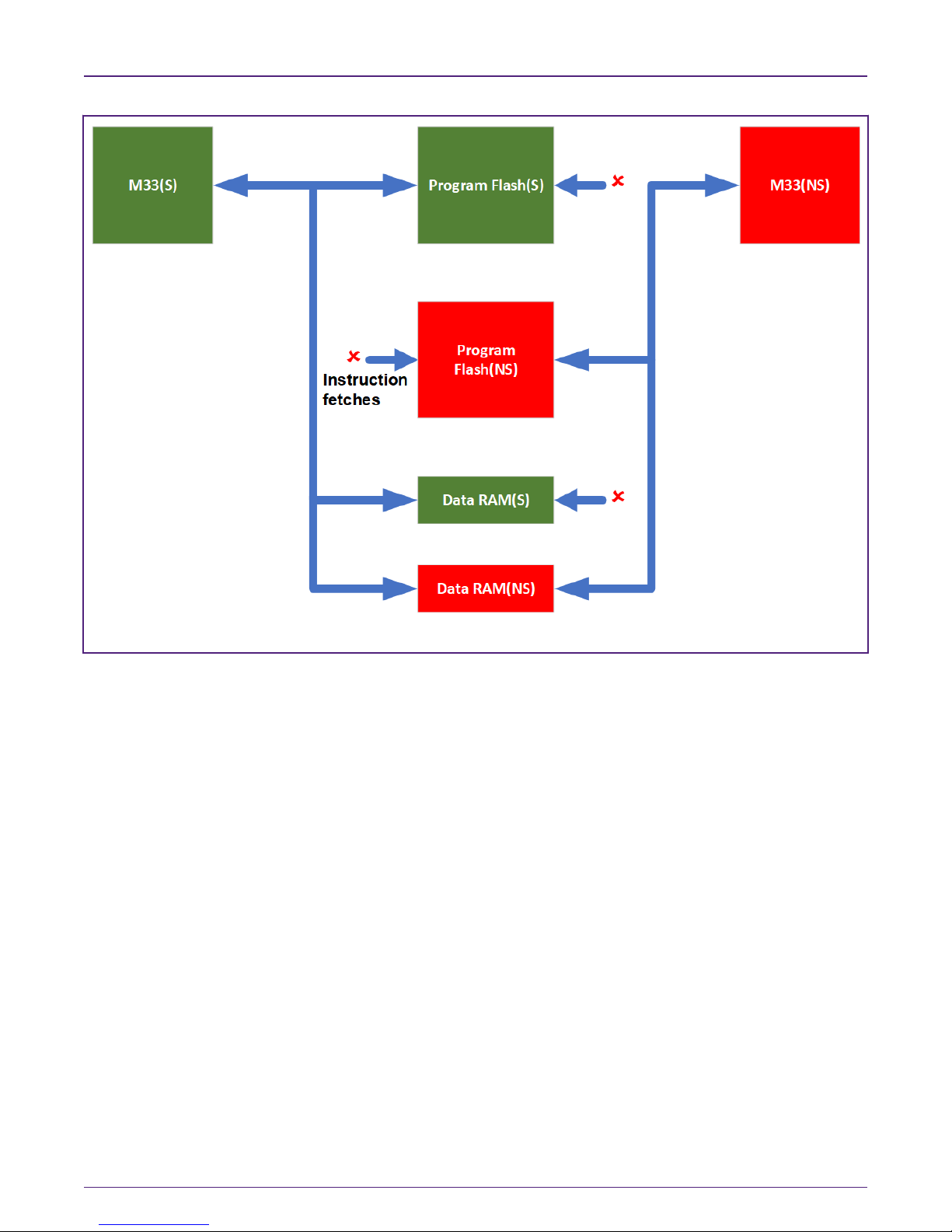
As shown in Fig 1, CM33 CPU in Secure state (CPU-S) can execute
instructions from Secure memory (S-memory), but not allowed to execute
instructions directly from Non-secure memory (NS-memory). However, CPUS can access data in both S-memory and NS-memory. CPU-NS can execute
instructions only from NS-memory, and not allowed to execute instructions from
S-memory. CPU-NS can access data only in NS-memory, but not allowed to access data from S-memory.
1 Background..........................................1
1.1 TrustZone and Secure
AHB Controller........................ 1
1.2 Normal GPIO...........................3
2 Secure GPIO, Secure GPIO Mask
and Secure PINT................................4
2.1 Secure GPIO Mask.................6
2.2 Secure GPIO...........................6
2.3 Secure PINT........................... 6
3 Usage.................................................... 6
3.1 Use Secure GPIO Mask to
protect Secure digital
peripherals which need IO...... 6
3.2 Set one IO to Secure GPIO.... 7
3.3 Usage of Secure PINT............8
4 Example................................................ 9
4.1 Environment............................9
4.2 Steps and result......................9
5 Conclusion..........................................11
6 Revision history................................. 11
Application Note
Page 2
NXP Semiconductors
Background
Figure 1. Secure state and Non-secure state view for TrustZone
In summary:
• NS application code “trust” that secure code, does not corrupt/modify NS code or data inadvertently or on purpose to create
malfunction or hazard
• S application code does not “trust” NS application code and disallows access to a CPU-NS
1.1.2 Secure AHB Controller
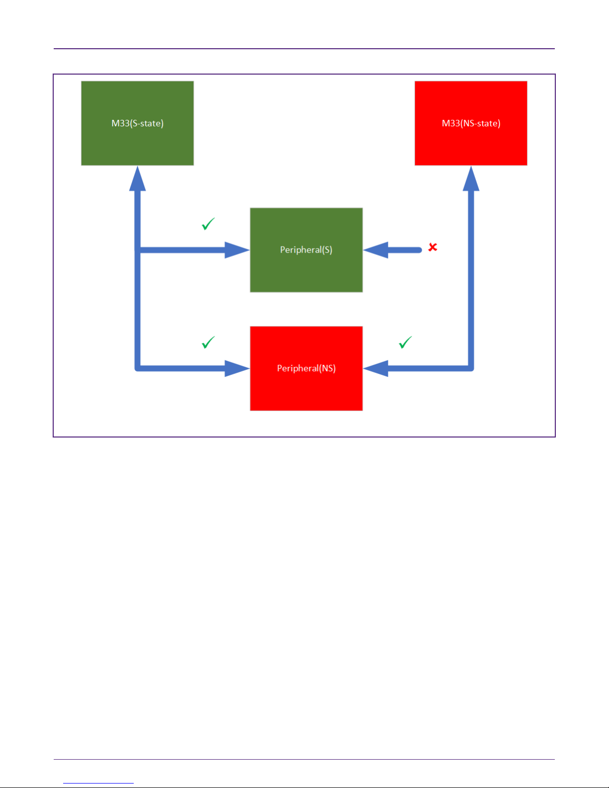
The LPC55S6x implements second layer of protection with Secure AHB Controller to provide secure trusted execution at systemlevel.
With Secure AHB Controller, you can configure security access rules for each peripheral.
By default, CM33 CPU in Secure state (CPU-S) can access the peripherals in both S-state and NS-state. CM33 CPU in Nonsecure state (CPU-NS) can only access the peripherals in NS-state. As shown in Fig 2.
LPC55S6x Secure GPIO and Usage, Rev. 0, 15 January 2019
Application Note
2 / 12
Page 3
NXP Semiconductors
Background
Figure 2. Secure-state and Non-secure state view for TrustZone and Secure AHB Controller
1.2 Normal GPIO
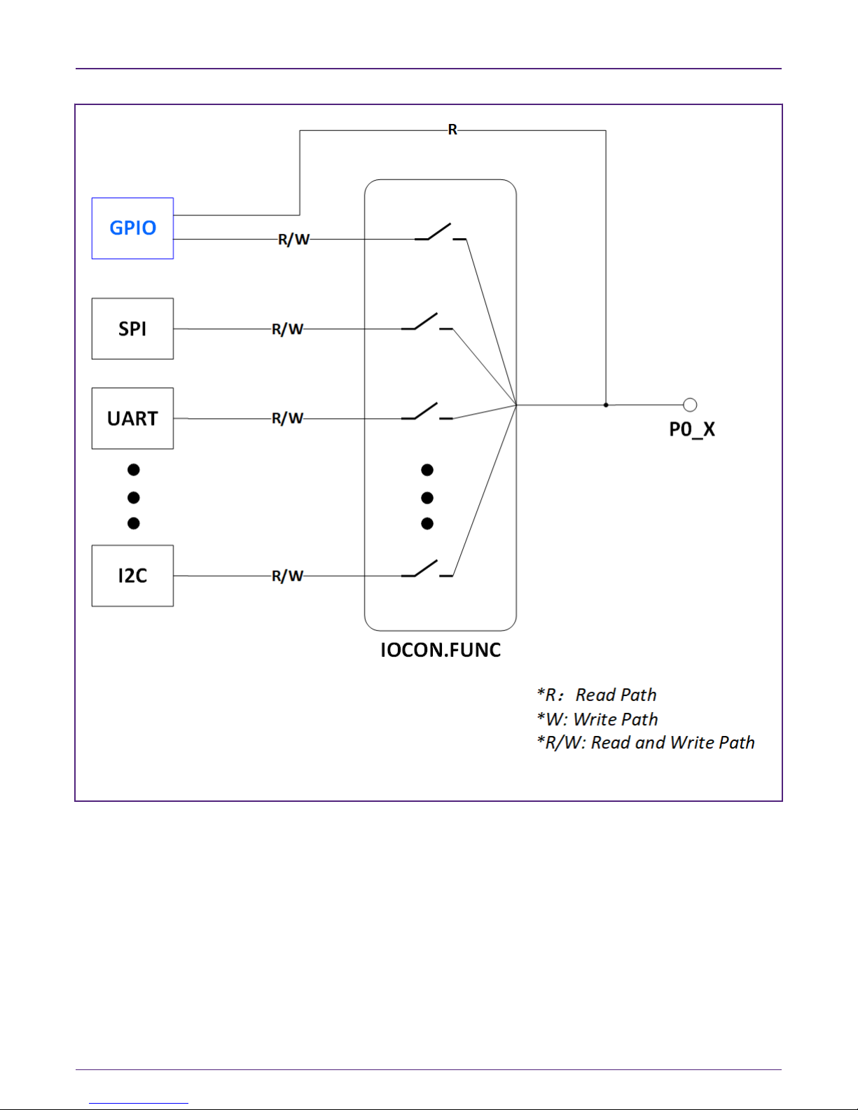
Normal GPIO is the most common digital peripheral in a microcontroller. Normal GPIO of LPC MCU is very flexible and powerful.
Like SPI, UART and so on, a normal GPIO is also a digital peripheral in the MCU. Following is a simple block diagram of the
normal GPIO. The normal GPIO can read a pin state regardless of pin function configured. For example, if this pin is configured
as UART, then the pin state can be read via normal GPIO read.
LPC55S6x Secure GPIO and Usage, Rev. 0, 15 January 2019
Application Note
3 / 12
Page 4
NXP Semiconductors
Secure GPIO, Secure GPIO Mask and Secure PINT
Figure 3. Normal GPIO
2 Secure GPIO, Secure GPIO Mask and Secure PINT
Due to the architecture of normal GPIO, all digital IO pins states are readable through normal GPIO module from the GPIO read
path, independent of which function is chosen for this pin as aforementioned. As a result, there is a possibility of leaking information
from secure resource(S).
For example, when a UART is configured as a Secure peripheral, which means that this UART is only allowed to be accessed by
the Secure-world (i.e. code), not by the Non-secure world.
However, in this case, the UART pin states can still be monitored by Non-secure world through normal GPIO read path as shown
in Fig 3. Hence, the Non-secure world can get all the Secure UART’s information.
To solve this issue and safeguard incoming data on Secure peripherals, Secure GPIO Mask is implemented on LPC55S6x.
LPC55S6x Secure GPIO and Usage, Rev. 0, 15 January 2019
Application Note
4 / 12
Page 5

NXP Semiconductors
Secure GPIO, Secure GPIO Mask and Secure PINT
In addition, if Secure-world need operate GPIO, it cannot use normal GPIO as normal GPIO is masked. In this case, a new
module, named Secure GPIO is introduced on LPC55S6x. Unlike normal GPIO, this Secure GPIO functionality is available only
if FUNC=10 in IOCON. It can be used to generate certain input pattern from external device for secure signaling.
For the same reason, Secure-world needs Secure Pin Interrupt/Pattern Match Engine (PINT), so another module named Secure
PINT is implemented.
The Fig.4 is a simple block diagram of the Secure GPIO and Secure GPIO Mask.
Figure 4. Secure GPIO and Secure GPIO Mask
LPC55S6x Secure GPIO and Usage, Rev. 0, 15 January 2019
Application Note
5 / 12
Page 6

NXP Semiconductors
Usage
2.1 Secure GPIO Mask
Each GPIO has a Secure GPIO MASK. As shown in Fig 4 , we can think of the Secure GPIO Mask as one input of the AND gate.
Its default value is 1. Through Secure GPIO Mask, we can control the on/off state of the normal GPIO read path.
2.2 Secure GPIO
As shown in Fig 4 , Secure GPIO has the same functions as normal GPIO. However, the access rules to this Secure GPIO for
different secure levels are configured through the Secure AHB controller which can only be accessed in Secure state.
2.3 Secure PINT
The main difference between Secure PINT and PINT is that the Secure PINT only supports up to two pins on Port 0. Similar as
Secure GPIO, the access rules to this module are configured through the Secure AHB controller.
The Secure Pin Interrupt Generator and the Secure Pattern Match Engine are available on all LPC55S6x devices.
Similar as normal PINT, the Secure Pin Interrupt Generator, and the Secure Pattern Match Engine are mutually exclusive.
2.3.1 Secure Pin Interrupts
– For Secure PINT block, up to two pins can be selected from all pins on port 0 , as edge-sensitive or level-sensitive interrupt
requests. Each request creates a separate interrupt in the NVIC.
– Edge-sensitive interrupt pins can interrupt on rising or falling edges or both.
– Level-sensitive interrupt pins can be HIGH-active or LOW-active.
2.3.2 Secure Pattern Match Engine
– Up to two pins can be selected from all digital pins on port 0 to contribute to a boolean expression. The boolean expression
consists of specified levels and/or transitions on various combinations of these pins.
– Each bit slice minterm (product term) comprising the specified boolean expression can generate its own, dedicated interrupt
request.
– Any occurrence of a pattern match can be programmed to generate an RXEV notification to the CPU.
– Pattern match can be used in conjunction with software, to create complex state machines based on pin inputs.
Usage
3
3.1 Use Secure GPIO Mask to protect Secure digital peripherals which need IO
SEC_GPIO_MASK register is used for controlling Secure GPIO Mask. Default register value is all 1, which means NS code can
still read Secure peripheral states by reading its pin states as shown in left side of Fig 5 below.
To prevent this risk of secure information leakage, the normal GPIO shall be masked by setting the corresponding bits in
SEC_GPIO_MASK to 0, as shown in the right side of Fig 5 below.
LPC55S6x Secure GPIO and Usage, Rev. 0, 15 January 2019
Application Note
6 / 12
Page 7

NXP Semiconductors
Figure 5. Usage of SEC_GPIO_MASK
Usage
The following code snippet shows how to mask P0_5 pin by using Secure GPIO MASK:
Figure 6. Set the SEC_GPIO_MASK of P0_5 to 0
3.2 Set one IO to Secure GPIO
Following are the steps to configure an I/O pin to Secure pin:
– Configure the corresponding bit of SEC_GPIO_MASK to 0.
– Configure the Secure GPIO module to Secure through Secure AHB Controller, It prevents Non-secure world from accessing
the Secure GPIO.
– Configure the IOCON block to Secure through Secure AHB Controller, It prevents Non-secure world from accessing the IOCON.
– Configure the corresponding pin function to Secure GPIO (FUNC=10) through Secure IOCON block.
– Enable Secure GPIO clock.
Afterwards, you can use it like a normal GPIO pin.
The following code snippets take P0_5 pin as an example.
–Configure the SEC_GPIO_MASK of P0_5 to 0:
Figure 7. Set the SEC_GPIO_MASK of P0_5 to 0
LPC55S6x Secure GPIO and Usage, Rev. 0, 15 January 2019
Application Note
7 / 12
Page 8

NXP Semiconductors
– Make the Secure GPIO IP Secure:
Figure 8. Make the Secure GPIO IP Secure
– Make the IOCON block Secure:
Figure 9. Make the IOCON block Secure
– Configure P0_5 pin function to Secure GPIO (FUNC=10):
Usage
Figure 10. Configure P0_5 pin function to Secure GPIO (FUNC=0xA)
– Enable Secure GPIO clock:
Figure 11. Enable Secure GPIO clock
3.3 Usage of Secure PINT
From application perspective, the method of using Secure PINT is same as of normal PINT.
There is one thing that needs extra attention:
– To disable the Non-secure world from accessing the Secure PINT register, set the Secure PINT to Secure through Secure AHB
Controller.
– Then you can use it like normal PINT and use the same APIs as normal PINT.
The code snippets for above settings are as shown below.
– Make the Secure PINT register Secure:
LPC55S6x Secure GPIO and Usage, Rev. 0, 15 January 2019
Application Note
8 / 12
Page 9

NXP Semiconductors
Figure 12. Make the Secure PINT register Secure
4 Example
4.1 Environment
4.1.1 Hardware environment
• Board
— LPCXpresso55S69(LPC55S69-EVK Revision 2)
• Debugger
— Integrated CMSIS-DAP debugger on the board
Example
• Miscellaneous
— 1 Micro USB cable
— PC
• Board Setup
— Connect the micro USB cable between PC and P6 link on the board for loading and running a demo.
4.1.2 Software environment
• Tool chain
— IAR embedded workbench 8.30.1
• Software package
— AN_SecureGPIO_Demo.zip
Steps and result
4.2
This example demonstrates how to use Secure GPIO.
The basic steps are as follows:
Configuration
1.
• Open the “secure_gpio_s” project located in the path as shown below.
LPC55S6x Secure GPIO and Usage, Rev. 0, 15 January 2019
Application Note
9 / 12
Page 10

NXP Semiconductors
Figure 13. Location of the demo project
There are two projects in the workspace.
Example
Figure 14. Demo projects
• Configure “secure_gpio_s” and “secure_gpio_ns” projects as shown below:
Figure 15. Configuration of the projects
Compile & Download
2.
• Compile “secure_gpio_s” project first, then compile “secure_gpio_ns” project.
LPC55S6x Secure GPIO and Usage, Rev. 0, 15 January 2019
Application Note
10 / 12
Page 11

NXP Semiconductors
• Connect the micro USB cable between PC and P6 link on the board while pressing and holding down ISP button.
• Download compiled executable file.
• Release ISP button after the download is successful.
Run
3.
Reset the board to run by pressing the Reset (S4) button on the board.
Result
4.
Two LEDs are used in this example. Blue LED indicates the pin state is read by normal GPIO, whereas green LED indicates
the pin stateis read by Secure GPIO. After reset, code is running in Secure world, and it initializes the system including
above two LEDs, and then it jumps to Non-secure world. In Non-secure world, it reads P0_5 pin (ISP button/S1 on EVK)
via both normal GPIO and Secure GPIO and the pin state it reads is 1 since this pin is pulled up externally by default. P0_5
will be read as 0 when ISP button is pressed and hold down, If P0_5 is 0, it turns on the blue LED and green LED as now
both normal GPIO and Secure GPIO read all 0 from this pin.
Press USER button (S3), it jumps to Secure world, toggle Secure GPIO Mask, and then jump back to Non-Secure world.
Press WAKEUP button (S2), it will jump to Secure world, make Secure GPIO Secure, and then jump back to Non-secure
world. At last, it tries to access the Secure GPIO from Non-Secure world, because of Secure access violation, it enters
Hard Fault. The following figure simply depicts its control flow:
Conclusion
Figure 16. Flow of Secure GPIO example
5 Conclusion
The example shows that Non-secure world can access a peripheral pin state regardless of the pin function and whether the
peripheral function is Secure or Non-secure. It results in Secure information leakage. To prevent, a Secure GPIO must be used
and it shall be configured and used in Secure world. Whereas, the normal GPIO shall be used in Non-secure world. Same rules
apply to Secure PINT and normal PINT.
6
Revision history
Revision Date Substantial Changes
0 15/01/2019 initial version
LPC55S6x Secure GPIO and Usage, Rev. 0, 15 January 2019
Application Note
11 / 12
Page 12

How To Reach Us
Home Page:
nxp.com
Web Support:
nxp.com/support
Information in this document is provided solely to enable system and software implementers to
use NXP products. There are no express or implied copyright licenses granted hereunder to
design or fabricate any integrated circuits based on the information in this document. NXP
reserves the right to make changes without further notice to any products herein.
NXP makes no warranty, representation, or guarantee regarding the suitability of its products for
any particular purpose, nor does NXP assume any liability arising out of the application or use
of any product or circuit, and specifically disclaims any and all liability, including without limitation
consequential or incidental damages. “Typical” parameters that may be provided in NXP data
sheets and/or specifications can and do vary in different applications, and actual performance
may vary over time. All operating parameters, including “typicals,” must be validated for each
customer application by customer's technical exper ts. NXP does not convey any license under
its patent rights nor the rights of others. NXP sells products pursuant to standard terms and
conditions of sale, which can be found at the following address: nxp.com/
SalesTermsandConditions.
While NXP has implemented advanced security features, all products may be subject to
unidentified vulnerabilities. Customers are responsible for the design and operation of their
applications and products to reduce the effect of these vulnerabilities on customer’s applications
and products, and NXP accepts no liability for any vulnerability that is discovered. Customers
should implement appropriate design and operating safeguards to minimize the risks associated
with their applications and products.
NXP, the NXP logo, NXP SECURE CONNECTIONS FOR A SMARTER WORLD, COOLFLUX,
EMBRACE, GREENCHIP, HITAG, I2C BUS, ICODE, JCOP, LIFE VIBES, MIFARE, MIFARE
CLASSIC, MIFARE DESFire, MIFARE PLUS, MIFARE FLEX, MANTIS, MIFARE ULTRALIGHT,
MIFARE4MOBILE, MIGLO, NTAG, ROADLINK, SMARTLX, SMARTMX, STARPLUG, TOPFET,
TRENCHMOS, UCODE, Freescale, the Freescale logo, AltiVec, C‑5, CodeTEST, CodeWarrior,
ColdFire, ColdFire+, C‑Ware, the Energy Efficient Solutions logo, Kinetis, Layerscape, MagniV,
mobileGT, PEG, PowerQUICC, Processor Expert, QorIQ, QorIQ Qonverge, Ready Play,
SafeAssure, the SafeAssure logo, StarCore, Symphony, VortiQa, Vybrid, Airfast, BeeKit,
BeeStack, CoreNet, Flexis, MXC, Platform in a Package, QUICC Engine, SMARTMOS, Tower,
TurboLink, and UMEMS are trademarks of NXP B.V. All other product or service names are the
property of their respective owners. AMBA, Arm, Arm7, Arm7TDMI, Arm9, Arm11, Artisan,
big.LITTLE, Cordio, CoreLink, CoreSight, Cortex, DesignStart, DynamIQ, Jazelle, Keil, Mali,
Mbed, Mbed Enabled, NEON, POP, RealView, SecurCore, Socrates, Thumb, TrustZone, ULINK,
ULINK2, ULINK-ME, ULINK-PLUS, ULINKpro, µVision, Versatile are trademarks or registered
trademarks of Arm Limited (or its subsidiaries) in the US and/or elsewhere. The related
technology may be protected by any or all of patents, copyrights, designs and trade secrets. All
rights reserved. Oracle and Java are registered trademarks of Oracle and/or its affiliates. The
Power Architecture and Power.org word marks and the Power and Power.org logos and related
marks are trademarks and service marks licensed by Power.org.
©
NXP B.V. 2019. All rights reserved.
For more information, please visit: http://www.nxp.com
For sales office addresses, please send an email to: salesaddresses@nxp.com
Date of release: 15 January 2019
Document identifier: AN12326
 Loading...