

Page 1

1. Introduction
1.1 About this document
1.2 Intended audience
DRAFT
D
RAFT DRAFT DRAFT DRAFT DRAFT D
D
RAFT DRA
D
RAFT
DR
AFT
DRAFT
LPC2917/19
ARM9 microcontroller with CAN and LIN
Rev. 1.01 — 15 November 2007 Preliminary data sheet
This document lists detailed information about the LPC2917/19 device. It focuses on
factual information like pinning, characteristics etc. Short descriptions are used to outline
the concept of the features and functions. More details and background on developing
applications for this device are given in the LPC2917/19 User Manual (see Ref. 1
explicit references are made to the User Manual.
This document is written for engineers evaluating and/or developing systems, hardand/or software for the LPC2917/19. Some basic knowledge of ARM processors and
architecture and ARM968E-S in particular is assumed (see Ref. 2
).
F
T DRAFT DRAFT DRAFT DRA
DRA
). No
DR
AFT
DRAFT
DR
F
T DRAF
2. General description
2.1 Architectural overview
The LPC2917/19 consists of:
• An ARM968E-S processor with real-time emulation support
• An AMBA multi-layer Advanced High-performance Bus (AHB) for interfacing to the
on-chip memory controllers
• Two DTL buses (a universal NXP interface) for interfacing to the interrupt controller
and the Power, Clock and Reset Control cluster (also called subsystem)
• Three VLSI Peripheral Buses (VPB - a compatible superset of ARM's AMBA
advanced peripheral bus) for connection to on-chip peripherals clu stered in
subsystems.
The LPC2917/19 configures the ARM968E-S processor in little-endian byte order. All
peripherals run at their own clock frequency to optimize the total system power
consumption. The AHB2VPB bridge used in the subsystems contains a write-ahead buffer
one transaction deep. This implies that when the ARM968E-S issues a buffered write
action to a register located on the VPB side of the bridge, it continues even though the
actual write may not yet have taken place. Completion of a second write to the same
subsystem will not be executed until the first write is finished.
Page 2

NXP Semiconductors
2.2 ARM968E-S processor
The ARM968E-S is a general purpose 32-bit RISC processor, which offers high
performance and very low power consumption. The ARM architecture is based on
Reduced Instruction Set Computer (RISC) principles, and the instruction set and related
decode mechanism are much simpler than those of micro-programmed Complex
Instruction Set Computers (CISC). This simplicity results in a high instruction throughput
and impressive real-time interrupt respon se from a sm all an d co st- effective contr olle r
core.
Amongst the most compelling features of the ARM968E-S are:
• Separate directly connected instruction and data Tightly Coupled Memory (TCM)
• Write buffers for the AHB and TCM buses
• Enhanced 16 x 32 multiplier capable of single-cycle MAC operations and 16-bit fixed-
DRAFT
ARM9 microcontroller with CAN and LIN
interfaces
point DSP instructions to accelerate signal-processing algorithms and applications.
D
RAFT DRAFT DRAFT DRAFT DRAFT D
D
LPC2917/19
RAFT DRA
D
RAFT
F
T DRAFT DRAFT DRAFT DRA
DR
AFT
DRAFT
DRAFT
DRA
F
DR
AFT
DR
T DRAF
Pipeline techniques are employed so that all part s of the pro cessing and memory systems
can operate continuously. The ARM968E-S is based on the ARMv5TE five-stage pipeline
architecture. Typically, in a three-stage pipeline architecture, while one instruction is being
executed its successor is being decoded and a third instruction is being fetched from
memory. In the five-stage pipeline additional stages are added for memory access and
write-back cycles.
The ARM968E-S processor also employs a unique architectural strategy known as
THUMB, which makes it ideally suited to high-volume applications with memory
restrictions or to applications where code density is an issue.
The key idea behind THUMB is that of a super-reduced instruction set. Essentially, the
ARM968E-S processor has two instruction sets:
• Standard 32-bit ARMv5TE set
• 16-bit THUMB set
The THUMB set's 16-bit instruction length allows it to approach twice the density of
standard ARM code while retaining most of the ARM's performance advantage over a
traditional 16-bit controller using 16-bit registers. This is possible because THUMB code
operates on the same 32-bit register set as ARM code.
THUMB code can provide up to 65 % of the code size of ARM, and 160 % of the
performance of an equivalent ARM controller connected to a 16-bit memory system.
The ARM968E-S processor is described in detail in the ARM968E-S data sheet Ref. 2
.
2.3 On-chip flash memory system
The LPC2917/19 includes a 512 kB or 768 kB flash memory system. This memory can be
used for both code and data storage. Programming of the flash memory can be
accomplished in several ways. It may be programmed in-system via a serial port; e.g.
CAN.
LPC2917_19_1 © NXP B.V. 2007. All rights reserved.
Preliminary data sheet Rev. 1.01 — 15 November 2007 2 of 68
Page 3

NXP Semiconductors
2.4 On-chip static RAM
In addition to the two 16 kB TCMs the LPC2917/19 includes two static RAM memories:
one of 32 kB and one of 16 kB. Both may be used for code and/or data storage. Each
internal SRAM has its own controller, so both me mo r ies ca n be acce ssed simultaneously
from different AHB system bus layers.
3. Features
3.1 General
ARM968E-S processor at 80 MHz maximum
Multi-layer AHB system bus at 80 MHz with three separate layers
On-chip memory:
Two-channel CAN controller supporting Full-CAN and extensive message filtering
Two LIN master controllers with full hardware support for LIN communication
Two 550 UARTs with 16-byte Tx and Rx FIFO depths
Three full-duplex Q-SPIs with four slave-select lines; 16 bits wide; 8 locations deep; Tx
Four 32-bit timers each containing four capture-and-compare registers linked to I/Os
32 - bit wa tch d og with tim er cha nge pr ot ection, running on safe clock.
Up to 108 general-purpose I/O pins with programmable pull-up, pull-down or bus
Vectored Interrupt Controller (VIC) with 16 priority levels
Two 8-channel 10-bit ADCs provide a total of up to 16 analog inputs, with conversion
Up to 24 level-sensitive external interrupt pins, including CAN and LIN wake- up
External Static Memory Controller (SMC) with eight memory banks; up to 32-bit data
Processor wake-up from power-down via external interrupt pins; CAN or LIN activity
Flexible Reset Generator Unit (RGU) able to control resets of individual modules
Flexible Clock-Generation Unit (CGU) able to control clock frequency of individual
DRAFT
ARM9 microcontroller with CAN and LIN
Two Tightly Coupled Memories (TCM), 16 kB Instruction (ITCM), 16 kB Data TCM
(DTCM)
Two separate internal Static RAM (SRAM) instances; 32 kB SRAM and 16 kB
SRAM
Up to 768 kB flash-program memory
FIFO and Rx FIFO
keeper
times as low as 2.44 μs per channel. Each channel provides a compare function to
minimize interrupts
features
bus; up to 24-bit address bus
modules
On-chip very low-power ring oscillator; fixed frequency of 0.4 MHz; always on to
provide a Safe_Clock source for system monitoring
On-chip crystal oscillator with operating range from 10 MHz to 50 MHz - max. PLL
input 15 MHz
On-chip PLL allows CPU operation up to a maximum CPU rate of 80 MHz
Generation of up to 10 base clocks
Seven fractional dividers
D
RAFT DRAFT DRAFT DRAFT DRAFT D
D
LPC2917/19
RAFT DRA
D
RAFT
F
T DRAFT DRAFT DRAFT DRA
DR
AFT
DRAFT
DRA
DR
AFT
DRAFT
DR
F
T DRAF
LPC2917_19_1 © NXP B.V. 2007. All rights reserved.
Preliminary data sheet Rev. 1.01 — 15 November 2007 3 of 68
Page 4

NXP Semiconductors
Highly configurable system Power Management Unit (PMU),
clock control of individual modules
allows minimization of system operating power consumption in any configuration
Standard ARM test and debug interface with real-time in-circuit emulator
Boundary-scan test supported
Du al po we r sup p ly:
CPU operating voltage: 1.8 V ± 5%
I/O operating voltage: 2.7 V to 3.6 V; inputs tolerant up to 5.5 V
14 4 -p i n LQ F P package
−40 °C to 85 °C ambient operating temperature range
4. Ordering information
DRAFT
ARM9 microcontroller with CAN and LIN
D
RAFT DRAFT DRAFT DRAFT DRAFT D
D
LPC2917/19
RAFT DRA
D
RAFT
DR
AFT
DRAFT
DRA
F
T DRAFT DRAFT DRAFT DRA
DR
AFT
DRAFT
DR
F
T DRAF
Table 1. Ordering information
Type number Package
LPC2917FBD144 LQFP144 plastic low profile quad flat package; 144 leads; body 20 × 20 × 1.4 mm, pin
LPC2919FBD144 LQFP144 plastic low profile quad flat package; 144 leads; body 20 × 20 × 1.4 mm, pin
Name Description Version
pitch 0.5 mm
pitch 0.5 mm
4.1 Ordering options
Table 2. Part options
Type number Flash memory
LPC2917FBD144 512 80 (incl TCMs) 32-bit 2 LQFP144
LPC2919FBD144 768 80 (incl TCMs) 32-bit 2 LQFP144
RAM (kB) SMC LIN 2.0 Package
(kB)
SOT486-1
SOT486-1
LPC2917_19_1 © NXP B.V. 2007. All rights reserved.
Preliminary data sheet Rev. 1.01 — 15 November 2007 4 of 68
Page 5
NXP Semiconductors
IEEE 1149.1 JTAG TEST and
DEBUG INTERFACE
LPC2917/19
DTCM
16 Kb
ITCM
16 Kb
ARM968E-S
m
s
s
s
s
s
s
s
s
s
Multi-layer AHB
system bus
m = master port
s = slave port
External Static Memory
Controller (SMC)
Embedded
SRAM Memory 32 Kb
SRAM Controller #0
Embedded
FLASH Memory
512/768 Kb
FLASH Memory Controller (FMC)
Embedded
SRAM Memory 16 Kb
SRAM Controller #1
GLOBAL ACCEPTANCE
FILTER
2 Kbyte Static RAM
LIN MASTER 0/1
CAN Controller
0, 1
Vectored Interrupt
Controller (VIC)
AHB2VPB
Bridge
AHB2DTL
Bridge
Modulation and Sampling
Control Subsystem
PWM 0, 1, 2, 3
ADC 1, 2
Timer 0, 1 (MTMR)
AHB2VPB
Bridge
Power Clock Reset
Control Subsystem
Power Management Unit (PMU)
Reset Generation Unit (RGU)
Clock Generation Unit (CGU)
AHB2DTL
Bridge
s
General Subsystem
Event Router (ER)
System Control Unit (SCU)
Chip Feature ID (CFID)
AHB2VPB
Bridge
Peripheral Subsystem
General Purpose IO (GPIO)
0, 1, 2, 3
Timer (TMR)
0, 1, 2, 3
Watchdog Timer (WDT)
UART 0, 1
AHB2VPB
Bridge
SPI 0, 1, 2
s
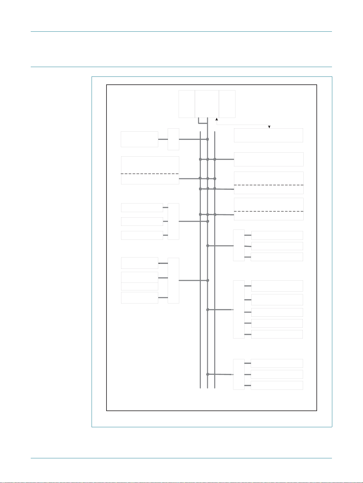
5. Block diagram
DRAFT
ARM9 microcontroller with CAN and LIN
D
RAFT DRAFT DRAFT DRAFT DRAFT D
D
LPC2917/19
RAFT DRA
D
RAFT
DR
AFT
DRAFT
DRA
F
T DRAFT DRAFT DRAFT DRA
DR
AFT
DRAFT
DR
F
T DRAF
Fig 1. LPC2917/19 block diagram
LPC2917_19_1 © NXP B.V. 2007. All rights reserved.
Preliminary data sheet Rev. 1.01 — 15 November 2007 5 of 68
Page 6
NXP Semiconductors
LPC2917FBD144
LPC2919FBD144
108
37
72
144
109
73
1
36
144PINS
6. Pinning information
6.1 Pinning
DRAFT
ARM9 microcontroller with CAN and LIN
D
RAFT DRAFT DRAFT DRAFT DRAFT D
D
LPC2917/19
RAFT DRA
D
RAFT
DR
AFT
DRAFT
DRA
F
T DRAFT DRAFT DRAFT DRA
DR
AFT
DRAFT
DR
F
T DRAF
Fig 2. Pin configuration for SOT486-1 (LQFP144)
6.2 Pin description
6.2.1 General description
The LPC2917/19 has up to four ports: two of 32 pins each, one of 28 pins and one of 16
pins. The pin to which each function is assigned is controlled by the SFSP registers in the
SCU. The functions combined on each port pin are shown in the pin description tables in
this section.
6.2.2 LQFP144 pin assignment
Table 3. LQFP144 pin assignment
Symbol Pin Description
TDO 1 IEEE 11 49.1 test data out
P2.21 2 GPIO 2, pin 21 - PWM2 CAP1 EXTBUS D19
P0.24 3 GPIO 0, pin 24 UART1 TxD CAN1 TxD SPI2 SCS0
P0.25 4 GPIO 0, pin 25 UART1 RxD CAN1 RxD SPI2 SDO
P0.26 5 GPIO 0, pin 26 - - SPI2 SDI
P0.27 6 GPIO 0, pin 27 - - SPI2 SCK
P0.28 7 GPIO 0, pin 28 - TIMER0 CAP0 TIMER0 MAT0
P0.29 8 GPIO 0, pin 29 - TIMER0 CAP1 TIMER0 MAT1
V
DD(IO)
P2.22 10 GPIO 2, pin 22 - PWM2 CAP2 EXTBUS D20
P2.23 11 GPIO 2, pin 23 - PWM3 CAP0 EXTBUS D21
P3.6 12 GPIO 3, pin 6 SPI0 SCS3 PWM1 MAT0 LIN1 TxD
P3.7 13 GPIO 3, pin 7 SPI2 SCS1 PWM1 MAT1 LIN1 RxD
P0.30 14 GPIO 0, pin 30 - TIMER0 CAP2 TIMER0 MAT2
P0.31 15 GPIO 0, pin 31 - TIMER0 CAP3 TIMER0 MAT3
LPC2917_19_1 © NXP B.V. 2007. All rights reserved.
Preliminary data sheet Rev. 1.01 — 15 November 2007 6 of 68
Function 0 (default) Function 1 Function 2 Function 3
9 3.3 V power supply for I/O
Page 7

DRAFT
NXP Semiconductors
D
RAFT DRAFT DRAFT DRAFT DRAFT D
D
LPC2917/19
RAFT DRA
D
RAFT
ARM9 microcontroller with CAN and LIN
F
T DRAFT DRAFT DRAFT DRA
Table 3. LQFP144 pin assignment
Symbol Pin Description
Function 0 (default) Function 1 Function 2 Function 3
P2.24 16 GPIO 2, pin 24 - PWM3 CAP1 EXTBUS D22
P2.25 17 GPIO 2, pin 25 - PWM3 CAP2 EXTBUS D23
V
DD(CORE)
V
SS(CORE)
P1.31 20 GPIO 1, pin 31 TIMER0 CAP1 TIMER0 MAT1 EXTINT5
V
SS(IO)
P1.30 22 GPIO 1, pin 30 TIMER0 CAP0 TIMER0 MAT0 EXTINT4
P3.8 23 GPIO 3, pin 8 SPI2 SCS0 PWM1 MAT2 P3.9 24 GPIO 3, pin 9 SPI2 SDO PWM1 MAT3 P1.29 25 GPIO 1, pin 29 TIMER1 CAP0, EXT
P1.28 26 GPIO 1, pin 28 TIMER1 CAP1, ADC1
P2.26 27 GPIO 2, pin 26 TIMER0 CAP2 TIMER0 MAT2 EXTINT6
P2.27 28 GPIO 2, pin 27 TIMER0 CAP3 TIMER0 MAT3 EXTINT7
P1.27 29 GPIO 1, pin 27 TIMER1 CAP2, ADC2
P1.26 30 GPIO 1, pin 26 PWM2 MAT0 PWM TRAP3 PWM3 MAT2
V
DD(IO)
P1.25 32 GPIO 1, pin 25 PWM1 MAT0 - PWM3 MAT1
P1.24 33 GPIO 1, pin 24 PWM0 MAT0 - PWM3 MAT0
P1.23 34 GPIO 1, pin 23 UART0 RxD - EXTBUS CS5
P1.22 35 GPIO 1, pin 22 UART0 TxD - EXTBUS CS4
TMS 36 IEEE 1149.1 test mode select, pulled up internally.
TCK 37 IEEE 1149.1 test clock
P1.21 38 GPIO 1, pin 21 TIMER3 CAP3 TIMER1 CAP3,
P1.20 39 GPIO 1, pin 20 TIMER3 CAP2 SPI0 SCS1 EXTBUS D6
P1.19 40 GPIO 1, pin 19 TIMER3 CAP1 SPI0 SCS2 EXTBUS D5
P1.18 41 GPIO 1, pin 18 TIMER3 CAP0 SPI0 SDO EXTBUS D4
P1.17 42 GPIO 1, pin 17 TIMER2 CAP3 SPI0 SDI EXTBUS D3
V
SS(IO)
P1.16 44 GPIO 1, pin 16 TIMER2 CAP2 SPI0 SCK EXTBUS D2
P2.0 45 GPIO 2, pin 0 TIMER2 MAT0 PWM TRAP3 EXTBUS D8
P2.1 46 GPIO 2, pin 1 TIMER2 MAT1 PWM TRAP2 EXTBUS D9
P3.10 47 GPIO 3, pin 10 SPI2 SDI PWM1 MAT4 P3.11 48 GPIO 3, pin 11 SPI2 SCK PWM1 MAT5 P1.15 49 GPIO 1, pin 15 TIMER2 CAP1 SPI0 SCS0 EXTBUS D1
P1.14 50 GPIO 1, pin 14 TIMER2 CAP0 SPI0 SCS3 EXTBUS D0
P1.13 51 GPIO 1, pin 13 EXTINT3 - EXTBUS WEN
P1.12 52 GPIO 1, pin 12 EXTINT2 - EXTBUS OEN
18 1.8 V power supply for digital core
19 ground for digital core
21 ground for I/O
31 3.3 V power supply for I/O
43 ground for I/O
…continued
PWM TRAP0 PWM3 MAT5
START
PWM TRAP1 PWM3 MAT4
EXT START
PWM TRAP2 PWM3 MAT3
EXT START
EXTBUS D7
MSCSS PAUSE
DR
AFT
DRAFT
DRA
DR
AFT
DRAFT
DR
F
T DRAF
LPC2917_19_1 © NXP B.V. 2007. All rights reserved.
Preliminary data sheet Rev. 1.01 — 15 November 2007 7 of 68
Page 8

DRAFT
NXP Semiconductors
D
RAFT DRAFT DRAFT DRAFT DRAFT D
D
LPC2917/19
RAFT DRA
D
RAFT
ARM9 microcontroller with CAN and LIN
F
T DRAFT DRAFT DRAFT DRA
Table 3. LQFP144 pin assignment
Symbol Pin Description
Function 0 (default) Function 1 Function 2 Function 3
V
DD(IO)
P2.2 54 GPIO 2, pin 2 TIMER2 MAT2 PWM TRAP1 EXTBUS D10
P2.3 55 GPIO 2, pin 3 TIMER2 MAT3 PWM TRAP0 EXTBUS D11
P1.11 56 GPIO 1, pin 11 SPI1 SCK - EXTBUS CS3
P1.10 57 GPIO 1, pin 10 SPI1 SDI - EXTBUS CS2
P3.12 58 GPIO 3, pin 12 SPI1 SCS0 EXTINT4 V
SS(CORE)
V
DD(CORE)
P3.13 61 GPIO 3, pin 13 SPI1 SDO EXTINT5 P2.4 62 GPIO 2, pin 4 TIMER1 MAT0 EXTINT0 EXTBUS D12
P2.5 63 GPIO 2, pin 5 TIMER1 MAT1 EXTINT1 EXTBUS D13
P1.9 64 GPIO 1, pin 9 SPI1 SDO LIN1 RxD EXTBUS CS1
V
SS(IO)
P1.8 66 GPIO 1, pin 8 SPI1 SCS0 LIN1 TxD EXTBUS CS0
P1.7 67 GPIO 1, pin 7 SPI1 SCS3 UART1 RxD EXTBUS A7
P1.6 68 GPIO 1, pin 6 SPI1 SCS2 UART1 TxD EXTBUS A6
P2.6 69 GPIO 2, pin 6 TIMER1 MAT2 EXTINT2 EXTBUS D14
P1.5 70 GPIO 1, pin 5 SPI1 SCS1 PWM3 MAT5 EXTBUS A5
P1.4 71 GPIO 1, pin 4 SPI2 SCS2 PWM3 MAT4 EXTBUS A4
TRSTN 72 I EEE 1149.1 test reset NOT; active LOW; pulled up internally
RSTN 73 asynchronous device reset; active LOW; pulled up internally
V
SS(OSC)
XOUT_OSC 75 crystal out for oscillator
XIN_OSC 76 crystal in for oscillator
V
DD(OSC)
V
SS(PLL)
P2.7 79 GPIO 2, pin 7 TIMER1 MAT3 EXTINT3 EXTBUS D15
P3.14 80 GPIO 3, pin 14 SPI1 SDI EXTINT6 CAN0 TxD
P3.15 81 GPIO 3, pin 15 SPI1 SCK EXTINT7 CAN0 RxD
V
DD(IO)
P2.8 83 GPIO 2, pin 8 - PWM0 MAT0 SPI0 SCS2
P2.9 84 GPIO 2, pin 9 - PWM0 MAT1 SPI0 SCS1
P1.3 85 GPIO 1, pin 3 SPI2 SCS1 PWM3 MAT3 EXTBUS A3
P1.2 86 GPIO 1, pin 2 SPI2 SCS3 PWM3 MAT2 EXTBUS A2
P1.1 87 GPIO 1, pin 1 EXTINT1 PWM3 MAT1 EXTBUS A1
V
SS(CORE)
V
DD(CORE)
P1.0 90 GPIO 1, pin 0 EXTINT0 PWM3 MAT0 EXTBUS A0
P2.10 91 GPIO 2, pin 10 - PWM0 MAT2 SPI0 SCS0
P2.11 92 GPIO 2, pin 11 - PWM0 MAT3 SPI0 SCK
53 3.3 V power supply for I/O
59 ground for digital core
60 1.8 V power supply for digital core
65 ground for I/O
74 ground for oscillator
77 1.8 V supply for oscillator
78 ground for PLL
82 3.3 V power supply for I/O
88 ground for digital core
89 1.8 V power supply for digital core
…continued
DR
AFT
DRAFT
DRA
DR
AFT
DRAFT
DR
F
T DRAF
LPC2917_19_1 © NXP B.V. 2007. All rights reserved.
Preliminary data sheet Rev. 1.01 — 15 November 2007 8 of 68
Page 9

DRAFT
NXP Semiconductors
D
RAFT DRAFT DRAFT DRAFT DRAFT D
D
LPC2917/19
RAFT DRA
D
RAFT
DRAFT
ARM9 microcontroller with CAN and LIN
F
T DRAFT DRAFT DRAFT DRA
Table 3. LQFP144 pin assignment
Symbol Pin Description
Function 0 (default) Function 1 Function 2 Function 3
P0.0 93 GPIO 0, pin 0 - CAN0 TxD EXTBUS D24
V
SS(IO)
P0.1 95 GPIO 0, pin 1 - CAN0 RxD EXTBUS D25
P0.2 96 GPIO 0, pin 2 - PWM0 MAT0 EXTBUS D26
P0.3 97 GPIO 0, pin 3 - PWM0 MAT1 EXTBUS D27
P3.0 98 GPIO 3, pin 0 - PWM2 MAT0 EXTBUS CS6
P3.1 99 GPIO 3, pin 1 - PWM2 MAT1 EXTBUS CS7
P2.12 100 GPIO 2, pin 12 - PWM0 MAT4 SPI0 SDI
P2.13 101 GPIO 2, pin 13 - PWM0 MAT5 SPI0 SDO
P0.4 102 GPIO 0, pin 4 - PWM0 MAT2 EXTBUS D28
P0.5 103 GPIO 0, pin 5 - PWM0 MAT3 EXTBUS D29
V
DD(IO)
P0.6 105 GPIO 0, pin 6 - PWM0 MAT4 EXTBUS D30
P0.7 106 GPIO 0, pin 7 - PWM0 MAT5 EXTBUS D31
V
DD(A3V3)
JTAGSEL 108 TAP controller select input; LOW-level selects the ARM debug mode; HIGH-level selects
NC 109 VREFP 1 10 HIGH reference for AD Converters
VREFN 111 LOW reference for AD Converters
P0.8 112 GPIO 0, pin 8 ADC1 IN0 LIN0 TxD EXTBUS A20
P0.9 113 GPIO 0, pin 9 ADC1 IN1 LIN0 RxD EXTBUS A21
P0.10 114 GPIO 0, pin 10 ADC1 IN2 PWM1 MAT0 EXTBUS A8
P0.11 115 GPIO 0, pin 11 ADC1 IN3 PWM1 MAT1 EXTBUS A9
P2.14 1 16 GPIO 2, pin 14 - PWM0 CAP0 EXTBUS BLS0
P2.15 1 17 GPIO 2, pin 15 - PWM0 CAP1 EXTBUS BLS1
P3.2 118 GPIO 3, pin 2 TIMER3 MAT0 PWM2 MAT2 V
SS(IO)
P3.3 120 GPIO 3, pin 3 TIMER3 MAT1 PWM2 MAT3 P0.12 121 GPIO 0, pin 12 ADC1 IN4 PWM1 MAT2 EXTBUS A10
P0.13 122 GPIO 0, pin 13 ADC1 IN5 PWM1 MAT3 EXTBUS A11
P0.14 123 GPIO 0, pin 14 ADC1 IN6 PWM1 MAT4 EXTBUS A12
P0.15 124 GPIO 0, pin 15 ADC1 IN7 PWM1 MAT5 EXTBUS A13
P0.16 125 GPIO 0, pin 16 ADC2 IN0 UART0 TXD EXTBUS A22
P0.17 126 GPIO 0, pin 17 ADC2 IN1 UART0 RXD EXTBUS A23
V
DD(CORE)
V
SS(CORE)
P2.16 129 GPIO 2, pin 16 UART1 TxD PWM0 CAP2 EXTBUS BLS2
P2.17 130 GPIO 2, pin 17 UART1 RxD PWM1 CAP0 EXTBUS BLS3
V
DD(IO)
94 ground for I/O
104 3.3 V power supply for I/O
107 3.3 V power supply for AD Converters
boundary scan and flash programming; pulled up internally
1 19 ground for I/O
127 1.8 V power supply for digital core
128 ground for digital core
131 3.3 V power supply for I/O
…continued
DR
AFT
DRA
DR
AFT
DRAFT
DR
F
T DRAF
LPC2917_19_1 © NXP B.V. 2007. All rights reserved.
Preliminary data sheet Rev. 1.01 — 15 November 2007 9 of 68
Page 10

DRAFT
NXP Semiconductors
D
RAFT DRAFT DRAFT DRAFT DRAFT D
D
LPC2917/19
RAFT DRA
D
RAFT
ARM9 microcontroller with CAN and LIN
F
T DRAFT DRAFT DRAFT DRA
Table 3. LQFP144 pin assignment
Symbol Pin Description
Function 0 (default) Function 1 Function 2 Function 3
P0.18 132 GPIO 0, pin 18 ADC2 IN2 PWM2 MAT0 EXTBUS A14
P0.19 133 GPIO 0, pin 19 ADC2 IN3 PWM2 MAT1 EXTBUS A15
P3.4 134 GPIO 3, pin 4 TIMER3 MAT2 PWM2 MAT4 CAN1 TxD
P3.5 135 GPIO 3, pin 5 TIMER3 MAT3 PWM2 MAT5 CAN1 RxD
P2.18 136 GPIO 2, pin 18 - PWM1 CAP1 EXTBUS D16
P2.19 137 GPIO 2, pin 19 - PWM1 CAP2 EXTBUS D17
P0.20 138 GPIO 0, pin 20 ADC2 IN4 PWM2 MAT2 EXTBUS A16
P0.21 139 GPIO 0, pin 21 ADC2 IN5 PWM2 MAT3 EXTBUS A17
P0.22 140 GPIO 0, pin 22 ADC2 IN6 PWM2 MAT4 EXTBUS A18
V
SS(IO)
P0.23 142 GPIO 0, pin 23 ADC2 IN7 PWM2 MAT5 EXTBUS A19
P2.20 143 GPIO 2, pin 20 - PWM2 CAP0 EXTBUS D18
TDI 144 IEEE 1149.1 data in, pulled up internally.
141 ground for I/O
…continued
DR
AFT
DRAFT
DRA
DR
AFT
DRAFT
DR
F
T DRAF
7. Functional description
7.1 Reset, debug, test and power description
7.1.1 Reset and power-up behavior
The LPC2917/19 contains external reset input and internal power-up reset circuits. This
ensures that a reset is extended internally until the oscillators and flash have reached a
stable state. See Section 11
Section 12
the reset pin.
Table 4. Reset pin
Symbol Direction Description
RSTN in external reset input, active LOW; pulled up internally
At activation of the RSTN pin the JTAGSEL pin is sensed as logic LOW. If this is the case
the LPC2917/19 is assumed to be connected to debug hardware, and internal circuits
re-program the source for the BASE_SYS_CLK to be the crystal oscillator instead of the
Low-Power Ring Oscillator (LP_OSC). This is required because the clock rate when
running at LP_OSC speed is too low for the external debugging environment.
7.1.2 Reset strategy
The LPC2917/19 contains a central module, the Reset Generator Unit (RGU) in the
Power, Clock and Reset Control Subsystem (PCRSS), which controls all internal reset
signals towards the peripheral modules. The RGU provides individua l reset control as well
as the monitoring functions needed for tracing a reset back to source.
for characteristics of the several start-up and initialization times. Table 4 shows
for trip levels of the internal power-up reset circuit1. See
1. Only for 1.8 V power sources
LPC2917_19_1 © NXP B.V. 2007. All rights reserved.
Preliminary data sheet Rev. 1.01 — 15 November 2007 10 of 68
Page 11

NXP Semiconductors
7.1.3 IEEE 1149.1 interface pins (JTAG boundary-scan test)
The LPC2917/19 contains boundary-scan test logic according to IEEE 1149.1, also
referred to in this document as Joint Test Action Group (JTAG). The boundary-scan test
pins can be used to connect a debugger probe for the embedded ARM processor. Pin
JTAGSEL selects between boundary-scan mode and debug mode. Table 5
boundary- scan test pins.
Table 5. IEEE 1149.1 boundary-scan test and debug interfa ce
Symbol Description
JTAGSEL TAP controller select input. LOW level selects ARM debug mode and HIGH level
TRSTN test reset input; pulled up internally (active LOW)
TMS test-mode select input; pulled up internally
TDI test data input, pulled up internally
TDO test data output
TCK test clock input
DRAFT
D
RAFT DRAFT DRAFT DRAFT DRAFT D
D
LPC2917/19
RAFT DRA
ARM9 microcontroller with CAN and LIN
F
selects boundary scan and flash programming; pulled up internally
D
RAFT
DR
DRAFT
T DRAFT DRAFT DRAFT DRA
AFT
DRA
DR
AFT
DRAFT
DR
F
T DRAF
shows the
7.1.4 Power supply pins description
Table 6 shows the power supply pins.
Table 6. Power supplies
Symbol Description
V
DD(CORE)
V
SS(CORE)
V
DD(IO)
V
SS(IO)
V
DD(OSC)
V
SS(OSC)
V
DD(A3V3)
V
SS(PLL)
digital core supply 1.8 V
digital core ground (digital core, ADC 1)
I/O pins supply 3.3 V
I/O pins ground
oscillator and PLL supply
oscillator ground
ADC 3.3 V supply
PLL ground
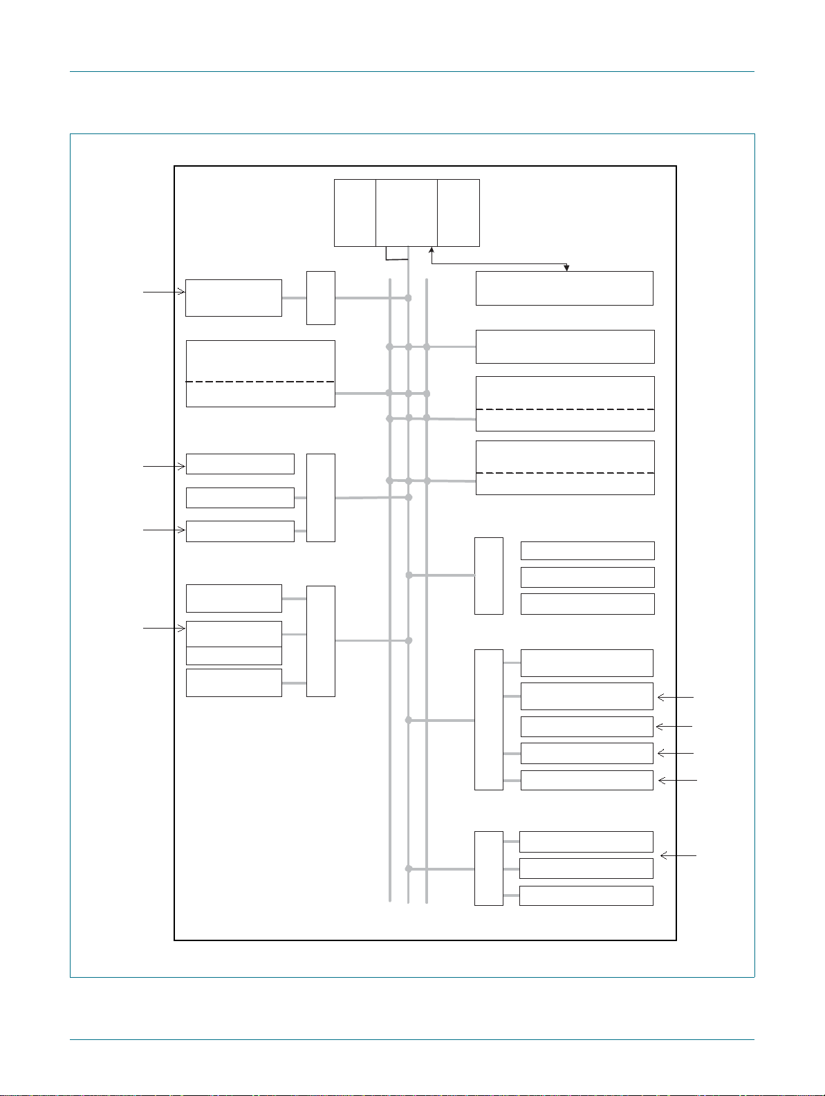
7.2 Clocking strategy
7.2.1 Clock architecture
The LPC2917/19 contains several different internal clock areas. Peripherals like Timers,
SPI, UART, CAN and LIN have their own individual clock sources called Base Clocks. All
base clocks are generated by the Clock Generator Unit (CGU). They may b e unre lated in
frequency and phase and can have different clock sources within the CGU.
The system clock for the CPU and AHB Multilayer Bus infrastructure has its own base
clock. This means most peripherals are clocked independently from the system clock. See
Figure 3
for an overview of the clock areas within the device.
Within each clock area there may be multiple branch clocks, which offers very flexible
control for power-management purposes. All branch clocks are outputs of the Power
Management Unit (PMU) and can be controlled independently. Branch clocks derived
from the same base clock are synchronous in frequency and phase. See Section 8.8
for
more details of clock and power control within the device.
LPC2917_19_1 © NXP B.V. 2007. All rights reserved.
Preliminary data sheet Rev. 1.01 — 15 November 2007 11 of 68
Page 12
NXP Semiconductors
General Subsystem
Event Router (ER)
System Control Unit (SCU)
Chip Feature ID (CFID)
AHB2VPB
Bridge
s
IEEE 1149.1 JTAG TEST and
DEBUG INTERFACE
LPC2917/19
DTCM
16 Kb
ITCM
16 Kb
ARM968E-S
m
s
s
s
s
s
s
s
s
s
External Static Memory
Controller (SMC)
Embedded
SRAM Memory 32 Kb
SRAM Controller #0
Embedded
FLASH Memory
512 - 768 Kb
FLASH Memory Controller (FMC)
Embedded
SRAM Memory 16 Kb
SRAM Controller #1
GLOBAL ACCEPTANCE
FILTER
2 Kbyte Static RAM
LIN MASTER 0/1
CAN Controller
0, 1
Vectored Interrupt
Controller (VIC)
AHB2VPB
Bridge
AHB2DTL
Bridge
Modulation and Sampling
Control Subsystem
PWM 0, 1, 2, 3
ADC 1, 2
Timer 0, 1 (MTMR)
AHB2VPB
Bridge
Power Clock Reset
Control Subsystem
Power Management Unit (PMU)
Reset Generation Unit (RGU)
Clock Generation Unit (CGU)
AHB2DTL
Bridge
Peripheral Subsystem
General Purpose IO (GPIO)
0, 1, 2, 3
Timer (TMR)
0, 1, 2, 3
Watchdog Timer (WDT)
UART 0, 1
AHB2VPB
Bridge
TMR_CLK
SAFE_CLK
UART_CLK
SPI_CLK
PCR_CLK
IVNSS_CLK
ADC_CLK
MSCSS_CLK
SYS_CLK
SPI 0, 1, 2
s
DRAFT
ARM9 microcontroller with CAN and LIN
D
RAFT DRAFT DRAFT DRAFT DRAFT D
D
LPC2917/19
RAFT DRA
D
RAFT
DR
AFT
DRAFT
DRA
F
T DRAFT DRAFT DRAFT DRA
DR
AFT
DRAFT
DR
F
T DRAF
Fig 3. LPC2917/19 block diagram, overview of clock areas
LPC2917_19_1 © NXP B.V. 2007. All rights reserved.
Preliminary data sheet Rev. 1.01 — 15 November 2007 12 of 68
Page 13

NXP Semiconductors
7.2.2 Base clock and branch clock relationship
The next table contains an overview of all the base blocks in the LPC2917/19 and their
derived branch clocks. A short description is given of the hardware parts that are clocked
with the individual branch clocks. In relevant cases more detailed information can be
found in the specific subsystem description. Some branch clocks have special protection
since they clock vital system parts of the device and shou ld (for example) not be switched
off. See Section 8.8.6
T able 7. Base clock and branch clock overview
Base clock Branch clock name Parts of the device clocked by
BASE_SAFE_CLK CLK_SAFE Watchdog Timer
BASE_SYS_CLK CLK_SYS_CPU ARM968E-S and TCMs
BASE_PCR_CLK CLK_PCR_SLOW PCRSS, CGU, RGU and PMU
BASE_IVNSS_CLK CLK_IVNSS_VPB VPB side of the IVNSS
DRAFT
D
RAFT DRAFT DRAFT DRAFT DRAFT D
D
LPC2917/19
RAFT DRA
D
RAFT
DR
DRAFT
ARM9 microcontroller with CAN and LIN
F
T DRAFT DRAFT DRAFT DRA
for more details of how to control the individual branch clocks.
Remark
this branch clock
[1]
CLK_SYS_SYS AHB Bus infrastructure
CLK_SYS_PCRSS AHB side of bridge in PCRSS
CLK_SYS_FMC Flash-Memory Controller
CLK_SYS_RAM0 Embedded SRAM Controller 0
(32 KByte)
CLK_SYS_RAM1 Embedded SRAM Controller 1
(16 KByte)
CLK_SYS_SMC External Static-Memory
Controller
CLK_SYS_GESS General Subsystem
CLK_SYS_VIC Vectored Interrupt Controller
CLK_SYS_PESS Peripheral Subsystem
CLK_SYS_GPIO0 GPIO bank 0
CLK_SYS_GPIO1 GPIO bank 1
CLK_SYS_GPIO2 GPIO bank 2
CLK_SYS_GPIO3 GPIO bank 3
CLK_SYS_IVNSS_A AHB side of bridge of IVNSS
logic clock
CLK_IVNSS_CANCA CAN controller Acceptance Filter
CLK_IVNSS_CANC0 CAN channel 0
CLK_IVNSS_CANC1 CAN channel 1
CLK_IVNSS_LIN0 LIN channel 0
CLK_IVNSS_LIN1 LIN channel 1
[2] [4]
[1], [3]
AFT
DRA
DR
AFT
DRAFT
DR
F
T DRAF
LPC2917_19_1 © NXP B.V. 2007. All rights reserved.
Preliminary data sheet Rev. 1.01 — 15 November 2007 13 of 68
Page 14

NXP Semiconductors
T able 7. Base clock and branch clock overview
Base clock Branch clock name Parts of the device clocked by
BASE_MSCSS_CLK CLK_MSCSS_VPB VPB side of the MSCSS
BASE_UART_CLK CLK_UART0 UART 0 interface clock
BASE_SPI_CLK CLK_SPI0 SPI 0 interface clock
BASE_TMR_CLK CLK_TMR0 Timer 0 clock for counter part
BASE_ADC_CLK CLK_ADC1 Control of ADC 1, capture sample
BASE_CLK_TESTSHELL CLK_TESTSHELL_IP
DRAFT
D
RAFT DRAFT DRAFT DRAFT DRAFT D
D
LPC2917/19
RAFT DRA
D
RAFT
ARM9 microcontroller with CAN and LIN
F
T DRAFT DRAFT DRAFT DRA
…continued
this branch clock
CLK_MSCSS_MTMR0 Timer 0 in the MSCSS
CLK_MSCSS_MTMR1 Timer 1 in the MSCSS
CLK_MSCSS_PWM0 PWM 0
CLK_MSCSS_PWM1 PWM 0
CLK_MSCSS_PWM2 PWM 0
CLK_MSCSS_PWM3 PWM 0
CLK_MSCSS_ADC1_VPBVPB side of ADC 1
CLK_MSCSS_ADC2_VPBVPB side of ADC 2
CLK_UART1 UART 1 interface clock
CLK_SPI1 SPI 1 interface clock
CLK_SPI2 SPI 2 interface clock
CLK_TMR1 Timer 1 clock for counter part
CLK_TMR2 Timer 2 clock for counter part
CLK_TMR3 Timer 3 clock for counter part
result
CLK_ADC2 Control of ADC 2, capture sample
result
DR
AFT
DRAFT
DRA
Remark
DR
AFT
DRAFT
DR
F
T DRAF
[1] This clock is always on (cannot be switched off for system safety reasons)
[2] In the peripheral subsystem parts of the Timers, Watchdog Timer, SPI and UART have their own clock
source. See Section 8.4
[3] In the Power Clock and Reset Control subsystem parts of the CGU, RGU PMU have their own clock
source. See Section 8.8
[4] The clock should remain activated w hen system wake-up on timer or UART is required.
for details.
for details.
8. Block description
8.1 Flash memory controller
8.1.1 Overview
The Flash Memory Controller (FMC) interfaces to the embedded flash memory for two
tasks:
• Providing memory data transfer
• Memory configuration via triggering, programming and erasing
LPC2917_19_1 © NXP B.V. 2007. All rights reserved.
Preliminary data sheet Rev. 1.01 — 15 November 2007 14 of 68
Page 15

NXP Semiconductors
The flash memory has a 128-bit wide data interface and the flash controller offers two
128-bit buffer lines to improve system performance. The flash has to be programmed
initially via JTAG. In-system programming must be supported by the boot loader.
In-application programming is possible. Flash memory contents can be protected by
disabling JTAG access. Suspension of burning or erasing is not supported.
The key features are:
• Programming by CPU via AHB
• Programming by external programmer via JTAG
• JTAG access protection
• Burn-finished and erase-finished interr up t
8.1.2 Description
DRAFT
ARM9 microcontroller with CAN and LIN
D
RAFT DRAFT DRAFT DRAFT DRAFT D
D
LPC2917/19
RAFT DRA
D
RAFT
F
T DRAFT DRAFT DRAFT DRA
DR
AFT
DRAFT
DRA
DR
AFT
DRAFT
DR
F
T DRAF
After reset flash initialization is started, which takes t
initialization flash access is not possible and AHB transfers to flash are stalled, blocking
the AHB bus.
During flash initialization the index sector is read to identify the status of the JTAG access
protection and sector security. If JTAG access protection is active the flash is not
accessible via JTAG. ARM debug facilities are disabled to protect the flash-memory
contents against unwanted reading out externally. If sector security is active only the
concerned sections are read.
Flash can be read synchronously or asynchronously to the system clock. In synchronous
operation the flash goes into standby after returning the read data. Started reads cannot
be stopped, and speculative reading and dual buff ering are therefore not supported.
With asynchronous reading, transfer of the address to the flash and of read da ta from the
flash is done asynchronously , giving the fastest possib le response time. S t arted reads can
be stopped, so speculative reading and dual buffering are supported.
Buffering is offered because the flash has a 128-bit wide data interface while the AHB
interface has only 32 bits. With buffering a buffer line holds the complete 128-bit flash
word, from which four words can be read. Without buffering every AHB data port read
starts a flash read. A flash read is a slow process compare d to the minimum AHB cycle
time, so with buffering the average read time is reduced. This can improve system
performance.
time, see Section 12. During this
init
With single buffering the most recently read flash word remains availabl e until the next
flash read. When an AHB data-port read transfer requires data from the same flash word
as the previous read transfer , no ne w flash read is done and the read dat a is given without
wait cycles.
When an AHB data-port read transfer requires data from a different flash word to that
involved in the previous read transfer, a new flash read is done and wait states are given
until the new read data is available.
With dual buffering a secondary buffer line is used, the output of the flash being
considered as the primary buffer. On a primary buffer hit data can be copied to the
secondary buffer line, which allows the flash to start a speculative read of the next flash
word.
LPC2917_19_1 © NXP B.V. 2007. All rights reserved.
Preliminary data sheet Rev. 1.01 — 15 November 2007 15 of 68
Page 16

NXP Semiconductors
Both buffer lines are invalidated after:
• Initialization
• Configuration-register access
• Data-latch reading
• Index-sector reading
DRAFT
ARM9 microcontroller with CAN and LIN
D
RAFT DRAFT DRAFT DRAFT DRAFT D
D
LPC2917/19
RAFT DRA
D
RAFT
DR
AFT
DRAFT
DRA
F
T DRAFT DRAFT DRAFT DRA
DR
AFT
DRAFT
DR
F
T DRAF
The modes of operation are listed in Table 8
Table 8. Flash read modes
Synchronous timing
No buffer line for single (non-linear) reads; one flash-word read per word read
Single buffer line default mo de of operation; most recently read flash word is kept until
another flash word is required
Asynchronous timing
No buffer line one flash-word read per word read
Single buffer line most recently read flash word is kept until another flash word is
required
Dual buffer line, single
speculative
Dual buffer line, always
speculative
on a buffer miss a flash read is done, followed by at most one
speculative read; optimized for execution of code with small loops
(less than eight words) from flash
most recently used flash word is copied into second buffer line; next
flash-word read is started; highest performance for linear reads
.
8.1.3 Flash memory controller pin description
The flash memory controller has no extern al pins. However, the flash can be programmed
via the JTAG pins, see Section 7.1.3
.
8.1.4 Flash memory controller clock description
The flash memory controller is clocked by CLK_SYS_FMC, see Section 7.2.2.
8.1.5 Flash layout
The ARM processor can program the flash for ISP (In-System Programming) a nd IAP (InApplication Programming). Note that the flash always has to be programmed by ‘flash
words’ of 128 bits (four 32-bit AHB bus words, hence 16 bytes).
The flash memory is organized into eight ‘small’ sectors of 8 kB each and up to 11 ‘large’
sectors of 64 kB each. The number of large sectors depends on the device type. A sector
must be erased before data can be written to it. The flash memory also has sector-wise
protection. Writing occurs per page which consists of 4096 bits (32 flash words). A small
sector contains 16 pages; a large sector contains 128 pages.
Table 9
Table 9. Flas h sector overview
Sector number Sector size (kB) Sector base address
0 8 0000 0000h
1 8 0000 2000h
2 8 0000 4000h
LPC2917_19_1 © NXP B.V. 2007. All rights reserved.
Preliminary data sheet Rev. 1.01 — 15 November 2007 16 of 68
gives an overview of the flash-sector base addresses.
Page 17

NXP Semiconductors
WST
t
acc clk()
t
t
tclk sys()
------------------
> 1–
WST
t
acc addr()
t
tclk sys()
--------------------- -
> 1–
Table 9. Flas h sector overview
Sector number Sector size (kB) Sector base address
3 8 0000 6000h
4 8 0000 8000h
5 8 0000 A000h
6 8 0000 C000h
7 8 0000 E000h
8 64 0001 0000h
9 64 0002 0000h
10 64 0003 0000h
11 64 0004 0000h
12 64 0005 0000h
13 64 0006 0000h
14 64 0007 0000h
[1]
15
[1]
16
[1]
17
[1]
18
ARM9 microcontroller with CAN and LIN
…continued
64 0008 0000h
64 0009 0000h
64 000A 0000h
64 000B 0000h
DRAFT
D
RAFT DRAFT DRAFT DRAFT DRAFT D
D
LPC2917/19
RAFT DRA
D
F
T DRAFT DRAFT DRAFT DRA
RAFT
DRAFT
DR
AFT
DRA
DR
AFT
DRAFT
DR
F
T DRAF
[1] Availability of sector 15 to sector 18 depends on device type, see Section 4 “Ordering information”.
The index sector is a special sector in which the JTAG access protection and sector
security are located. The address space becomes visible by setting the FS_ISS bit and
overlaps the regular flash sector’s address space.
Note that the index sector cannot be erased, and that acce ss to it ha s to be pe rformed via
code outside the flash.
8.1.6 Flash bridge wait-states
To eliminate the delay associated with synchronizing flash-read data, a predefined
number of wait-states must be programmed. These depend on flash-memory response
time and system clock period. The minimum wait-states value can be calculated with the
following formulas:
Synchronous reading:
Asynchronous reading:
LPC2917_19_1 © NXP B.V. 2007. All rights reserved.
Preliminary data sheet Rev. 1.01 — 15 November 2007 17 of 68
Page 18

NXP Semiconductors
Remark: If the programmed number of wait-states is more than three, flash-data reading
cannot be performed at full speed (i.e. with zero wait-states at the AHB bus) if speculative
reading is active.
8.2 External static memory controller
8.2.1 Overview
The LPC2917/19 contains an external Static Memory Controller (SMC) which provides an
interface for external (off-chip) memory devices.
Key features are:
• Supports static memory-mapped devices including RAM, ROM, flash, burst ROM and
• Asynchronous page-mode read operation in non-clocked memory subsystems
• Asynchronous burst-mode read access to burst-mode ROM devices
• Independent configuration for up to eight banks, each up to 16 MB
• Programmable bus-turnaround (idle) cycles (one to 16)
• Programmable read and write wait states (up to 32), for static RAM devices
• Programmable initial and subsequent burst-read wait state for burst-ROM devices
• Programmable write protection
• Programmable burst-mode operation
• Programmable external data width: 8-bit, 16-bit or 32-bit
• Programmable read-byte lane enable control
external I/O devices
DRAFT
ARM9 microcontroller with CAN and LIN
D
RAFT DRAFT DRAFT DRAFT DRAFT D
D
LPC2917/19
RAFT DRA
D
RAFT
F
T DRAFT DRAFT DRAFT DRA
DR
AFT
DRAFT
DRA
DR
AFT
DRAFT
DR
F
T DRAF
8.2.2 Description
The SMC simultaneously supports up to eigh t independently configurable memory banks.
Each memory bank can be 8, 16 or 32 bits wide and is capable of supporting SRAM,
ROM, burst-ROM memory or external I/O devices.
A separate chip-select output is available for each bank. The chip-select lines are
configurable to be active HIGH or LOW. Memory-bank selection is controlled by memory
addressing. Table 10
memory base addresses, chip selects and bank internal addresses.
Table 10. External memory-bank address bit description
32 bit
System
Address Bit
field
31 to 29 BA[2:0] external static-memory base address (three most significant bits);
28 to 26 CS[2:0] chip-select address space for eight memory banks; see
25 and 24 - always ’00’; other values are ’mirrors’ of the 16 MByte bank address
23 to 0 A[23:0] 16-MByte memory banks address space
shows how the 32-bit system address is mapped to the external bus
Symbol Description
the base address can be found in the memory map; see Ref. 1
field contains ’010’ when addressing an external memory bank.
. This
[1]
LPC2917_19_1 © NXP B.V. 2007. All rights reserved.
Preliminary data sheet Rev. 1.01 — 15 November 2007 18 of 68
Page 19

NXP Semiconductors
Table 11. External static-memory controller banks
CS[2:0] Bank
000 bank 0
001 bank 1
010 bank 2
011 bank 3
100 bank 4
101 bank 5
110 bank 6
111 bank 7
8.2.3 External static-memory controller pin description
The external static-memory controller module in the LPC2917/19 has the following pins,
which are combined with other functions on the port pins of the LPC2917/19. Table 12
shows the external memory controller pins.
Table 12. External memory controller pins
Symbol Direction Description
EXTBUS CSx out memory-bank x select, x runs from 0 to 7
EXTBUS BLSy out byte-lane select input y, y runs from 0 to 3
EXTBUS WE_N out write enable (active LOW)
EXTBUS OE_N out output enable (active LOW)
EXTBUS A[23:0] out address bus
EXTBUS D[31:0] in/out data bus
DRAFT
ARM9 microcontroller with CAN and LIN
D
RAFT DRAFT DRAFT DRAFT DRAFT D
D
LPC2917/19
RAFT DRA
D
RAFT
DR
AFT
DRAFT
DRA
F
T DRAFT DRAFT DRAFT DRA
DR
AFT
DRAFT
DR
F
T DRAF
8.2.4 External static-memory controller clock description
The External Static-Memory Controller is clocked by CLK_SYS_SMC, see Section 7.2.2.
8.2.5 External memory timing diagrams
A timing diagram for reading from external memory is shown in Figure 4. The relationship
between the wait-state settings is indicated with arrows.
LPC2917_19_1 © NXP B.V. 2007. All rights reserved.
Preliminary data sheet Rev. 1.01 — 15 November 2007 19 of 68
Page 20
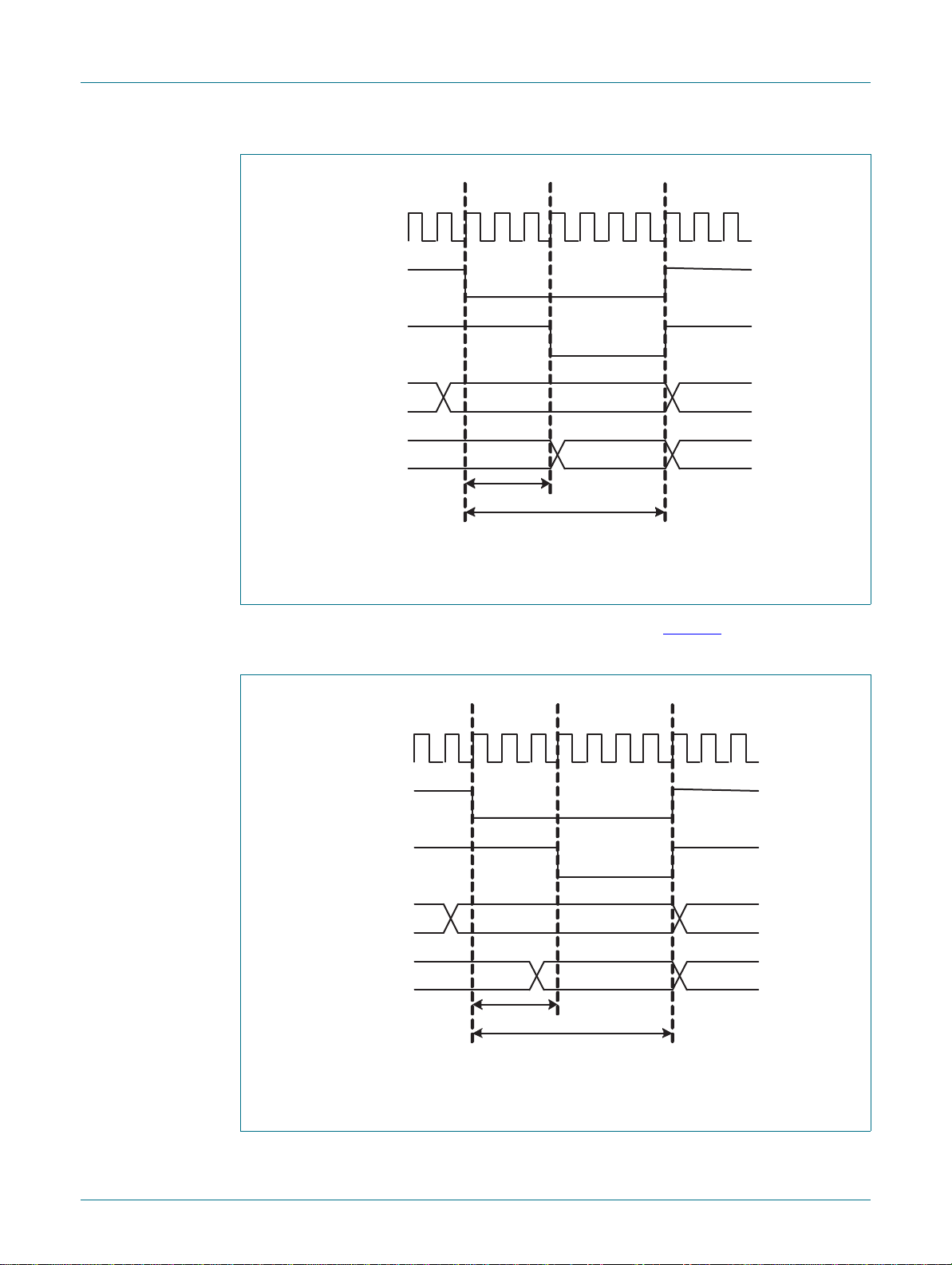
NXP Semiconductors
OE_N
CLK(SYS)
CS
ADDR
DATA
WSTOEN
WST1
CLK(SYS)
CS
ADDR
DATA
WSTWEN
WST2
WE_N / BLS
DRAFT
ARM9 microcontroller with CAN and LIN
D
RAFT DRAFT DRAFT DRAFT DRAFT D
D
LPC2917/19
RAFT DRA
D
RAFT
DR
AFT
DRAFT
DRA
F
T DRAFT DRAFT DRAFT DRA
DR
AFT
DRAFT
DR
F
T DRAF
WSTOEN=3, WST1=7
Fig 4. Reading from external memory
A timing diagram for writing to external memory is shown In Figure 5. The relationship
between wait-state settings is indicated with arrows.
WSTWEN=3, WST2=7
Fig 5. Writing to external memory
LPC2917_19_1 © NXP B.V. 2007. All rights reserved.
Preliminary data sheet Rev. 1.01 — 15 November 2007 20 of 68
Page 21
NXP Semiconductors
OE_N
CLK(SYS)
CS
ADDR
DATA
WSTOEN
WST1
WSTWEN
WST2
WE_N / BLS
IDCY
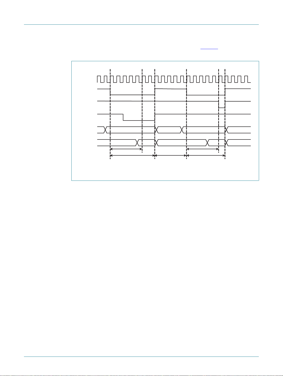
Usage of the idle/turn-around time (IDCY) is de mon str ated In Figure 6. Extra wait states
are added between a read and a write cycle in the same external memory device.
DRAFT
ARM9 microcontroller with CAN and LIN
D
RAFT DRAFT DRAFT DRAFT DRAFT D
D
LPC2917/19
RAFT DRA
D
RAFT
DR
AFT
DRAFT
DRA
F
T DRAFT DRAFT DRAFT DRA
DR
AFT
DRAFT
DR
F
T DRAF
WSTOEN=5, WSTWEN=5, WST1=7, WST2=6, IDCY=5
Fig 6. Reading/writing external memory
Address pins on the device are shared with other functions. When connecting external
memories, check that the I/O pin is programmed for the correct function. Control of these
settings is handled by the SCU.
LPC2917_19_1 © NXP B.V. 2007. All rights reserved.
Preliminary data sheet Rev. 1.01 — 15 November 2007 21 of 68
Page 22

NXP Semiconductors
8.3 General subsystem
8.3.1 General subsystem clock description
The general subsystem is clocked by CLK_SYS_GESS, see Section 7.2.2.
8.3.2 Chip and feature identification
8.3.2.1 Overview
The key features are:
• Identification of product
• Identification of features enabled
8.3.2.2 Description
The Chip/Feature ID (CFID) module contains registers which show and control the
functionality of the chip. It contains an ID to identify the silicon, and also registers
containing information about the features enabled or disabled on the chip.
DRAFT
ARM9 microcontroller with CAN and LIN
D
RAFT DRAFT DRAFT DRAFT DRAFT D
D
LPC2917/19
RAFT DRA
D
RAFT
F
T DRAFT DRAFT DRAFT DRA
DR
AFT
DRAFT
DRA
DR
AFT
DRAFT
DR
F
T DRAF
8.3.2.3 CFID pin description
The CFID has no external pins.
8.3.3 System Control Unit (SCU)
8.3.3.1 Overview
The system control unit takes care of system-related functions.The key feature is
configuration of the I/O port-pins multiplexer.
8.3.3.2 Description
The system control unit defines the function of each I/O pin of the LPC2917/19. The I/O
pin configuration should be consistent with peripheral function usage.
8.3.3.3 SCU pin description
The SCU has no external pins.
8.3.4 Event router
8.3.4.1 Overview
The event router provides bus-controlled routing of input events to the vectored interrupt
controller for use as interrupt or wake-up signals.
Key features:
• Up to 24 level-sensitive external interrupt pins, including CAN, LIN and RxD wake-up
features plus three internal event sources
• Input events can be used as interrupt source either directly or latched (edge-detected)
• Direct events disappear when the event becomes inactive
• Latched events remain active until they are explicitly cleared
• Programmable input level and edge polarity
• Event detection maskable
LPC2917_19_1 © NXP B.V. 2007. All rights reserved.
Preliminary data sheet Rev. 1.01 — 15 November 2007 22 of 68
Page 23

NXP Semiconductors
• Event detection is fully asynchronous, so no clock is required
8.3.4.2 Description
The event router allows the event source to be defined, its polarity and activation type to
be selected and the interrupt to be masked or enabled. The event router can be used to
start a clock on an external event.
The vectored interrupt-controller inputs are active HIGH.
8.3.4.3 Event-router pin description and mapping to register bit positions
The event router module in the LPC2917/19 is connected to the pins listed below. The
pins are combined with other functions on the port pins of the LPC2917/19. Table 13
shows the pins connected to the event router, and also the corresponding bit position in
the event-router registers and the default polarity.
Table 13. Event-router pin connections
Symbol Direction Bit position Description Default
EXTINT0 in 0 external interrupt input 0 1
EXTINT1 in 1 external interrupt input 1 1
EXTINT2 in 2 external interrupt input 2 1
EXTINT3 in 3 external interrupt input 3 1
EXTINT4 in 4 external interrupt input 4 1
EXTINT5 in 5 external interrupt input 5 1
EXTINT6 in 6 external interrupt input 6 1
EXTINT7 in 7 external interrupt input 7 1
CAN0 RXD in 8 CAN0 receive data input wake-up 0
CAN1 RXD in 9 CAN1 receive data input wake-up 0
- - 13 - 10 reserved LIN0 RXD in 14 LIN0 receive data input wake-up 0
LIN1 RXD in 15 LIN1 receive data input wake-up 0
- - 21 - 16 reserved -
- na 22 CAN interrupt (internal) 1
- na 23 VIC FIQ (internal) 1
- na 24 VIC IRQ (internal) 1
- - 26 - 25 reserved -
DRAFT
ARM9 microcontroller with CAN and LIN
D
RAFT DRAFT DRAFT DRAFT DRAFT D
D
LPC2917/19
RAFT DRA
D
RAFT
DR
AFT
DRAFT
DRA
F
T DRAFT DRAFT DRAFT DRA
polarity
DR
AFT
DRAFT
DR
F
T DRAF
8.4 Peripheral subsystem
8.4.1 Peripheral subsystem clock description
The peripheral subsystem is clocked by a number of different clocks:
• CLK_SYS_PESS
• CLK_UART0/1
• CLK_SPI0/1/2
• CLK_TMR0/1/2/3
LPC2917_19_1 © NXP B.V. 2007. All rights reserved.
Preliminary data sheet Rev. 1.01 — 15 November 2007 23 of 68
Page 24

NXP Semiconductors
• CLK_SAFE see Section 7.2.2
8.4.2 Watchdog timer
8.4.2.1 Overview
The purpose of the watchdog timer is to reset the ARM9 processor within a reasonable
amount of time if the processor enters an error state. The watchdog generates a system
reset if the user program fails to trigger it correctly within a predetermined amount of time.
Key features:
• Internal chip reset if not periodically triggered
• Timer counter register runs on always-on safe clock
• Optional interrupt generation on watchdog timeout
• Debug mode with disabling of reset
• Watchdog control register change-protected with key
• Programmable 32-bit watchdog timer period with programmable 32-bit prescaler.
DRAFT
ARM9 microcontroller with CAN and LIN
D
RAFT DRAFT DRAFT DRAFT DRAFT D
D
LPC2917/19
RAFT DRA
D
RAFT
F
T DRAFT DRAFT DRAFT DRA
DR
AFT
DRAFT
DRA
DR
AFT
DRAFT
DR
F
T DRAF
8.4.2.2 Description
The watchdog timer consists of a 32-bit counter with a 32-bit prescaler.
The watchdog should be programmed with a time-out value and then periodically
restarted. When the watchdog times out it generates a reset through the RGU.
To generate watchdog interrupts in watchdog debug mode the interr upt has to be enable d
via the interrupt enable register. A watchdog-overflow interrupt can be cleared by writing
to the clear-interrupt register.
Another way to prevent resets during debug mod e is via the Pause feature of the
Watchdog Timer. The watchdog is stalled when the ARM9 is in debug mode and the
PAUSE_ENABLE bit in the Watchdog Timer Control register is set.
The Watchdog Reset output is fed to the Reset Gener ator Unit (RGU). The RGU cont ains
a reset source register to identify the reset source when the device has gone through a
reset. See Section 8.8.5
8.4.2.3 Pin description
The watchdog has no external pins.
8.4.2.4 Watchdog timer clock description
The Watchdog Timer is clocked by two different clocks; CLK_SYS_PESS and
CLK_SAFE, see Section 7.2.2
by CLK_SYS_PESS. The timer and prescale counters are clocked by CLK_SAFE which
is always on.
.
. The register interface towards the system bus is clocked
8.4.3 Timer
8.4.3.1 Overview
The LPC2917/19 contains six identical timers: four in the peripheral subsystem and two in
the Modulation and Sampling Control SubSystem (MSCSS) located at d iffer ent peripher al
base addresses. This section describes the four timers in the peripheral subsystem. Each
LPC2917_19_1 © NXP B.V. 2007. All rights reserved.
Preliminary data sheet Rev. 1.01 — 15 November 2007 24 of 68
Page 25

NXP Semiconductors
timer has four capture inputs and/or match output s. Connection to device pins depends on
the configuration programmed into the port function-select registers. The two timers
located in the MSCSS have no external capture or match pins, but the memory map is
identical, see Section 8.7.7
function.
The key features are:
• 32-bit timer/counter with programm ab le 32 -b it pr es ca ler
• Up to four 32-bit capture channels per timer . These ta ke a snapshot of the time r value
• Four 32-bit match registers per timer that allow:
• Up to four external outputs per timer corresponding to match registers, with the
• Pause input pin (MSCSS timers only)
DRAFT
ARM9 microcontroller with CAN and LIN
. One of these timers has an external input for a pause
when an external signal connected to the TIMERx CAPn input changes state. A
capture event may also optionally generate an interrupt
– Continuous operation with optional interrupt generation on match
– Stop timer on match with optional interrupt generation
– Reset timer on match with optional interrupt generation
following capabilities:
– Set LOW on match
– Set HIGH on match
– Toggle on match
– Do nothing on match
D
RAFT DRAFT DRAFT DRAFT DRAFT D
D
LPC2917/19
RAFT DRA
D
RAFT
F
T DRAFT DRAFT DRAFT DRA
DR
DRAFT
AFT
DRA
DR
AFT
DRAFT
DR
F
T DRAF
8.4.3.2 Description
The timers are designed to count cycles of the clock and optionally generate interr upts or
perform other actions at specified timer values, based on four match registers. They also
include capture inputs to trap the timer value when an input sign al changes state,
optionally generating an interrupt. The core function of the timers consists of a 32 bit
‘prescale counter’ trig g er ing the 32 bit ‘timer cou nt er’. Both counters run on cl oc k
CLK_TMRx (x runs from 0 to 3) and all time references are related to the period of this
clock. Note that each timer has its individual clock source within the Peripheral
SubSystem. In the Modulation and Sampling SubSystem each timer also has its own
individual clock source. See section Section 8.8.6
clocks.
8.4.3.3 Pin description
The four timers in the peripheral subsystem of the LPC2917/19 have the pins described
below. The two timers in the modulation and sampling subsystem have no external pins
except for the pause pin on MSCSS timer 1. See Section 8.7.7
timers and their associated pins. The timer pins are combined with other functions on the
port pins of the LPC2917/19, see Section 8.3.3
runs from 0 to 3).
for information on generation of these
for a description of these
. Table Table 14 shows the timer pins (x
LPC2917_19_1 © NXP B.V. 2007. All rights reserved.
Preliminary data sheet Rev. 1.01 — 15 November 2007 25 of 68
Page 26

NXP Semiconductors
Table 14. Timer pins
Symbol Direction Description
TIMERx CAP[0] IN TIMER x capture input 0
TIMERx CAP[1] IN TIMER x capture input 1
TIMERx CAP[2] IN TIMER x capture input 2
TIMERx CAP[3] IN TIMER x capture input 3
TIMERx MAT[0] OUT TIMER x match output 0
TIMERx MAT[1] OUT TIMER x match output 1
TIMERx MAT[2] OUT TIMER x match output 2
TIMERx MAT[3] OUT TIMER x match output 3
8.4.3.4 Timer clock description
The timer modules are clocked by two different clocks; CLK_SYS_PESS and CLK_TMRx
(x = 0-3), see Section 7.2.2
power management. The frequency of all these clocks is identical as they are derived
from the same base clock BASE_CLK_TMR. The register interface towards the system
bus is clocked by CLK_SYS_PESS. The timer and prescale counters are clocked by
CLK_TMRx.
DRAFT
ARM9 microcontroller with CAN and LIN
D
RAFT DRAFT DRAFT DRAFT DRAFT D
D
LPC2917/19
RAFT DRA
D
RAFT
DR
AFT
DRAFT
DRA
F
T DRAFT DRAFT DRAFT DRA
. Note that each timer has its own CLK_TMRx branch clock for
DR
AFT
DRAFT
DR
F
T DRAF
8.4.4 UARTs
8.4.4.1 Overview
The LPC2917/19 contains two identical UARTs located at different peripheral base
addresses. The key features are:
• 16-byte receive and transmit FIFOs
• Registers conform to industry standard 550
• Receiver FIFO trigger points at 1 byte, 4 bytes, 8 bytes and 14 bytes
• Built-in baud-rate generator
8.4.4.2 Description
The UART is commonly used to implement a serial interface such as RS232. The
LPC2917/19 contains two industry-st andard 550 UAR Ts with 16-byte transmit and receive
FIFOs, but they can also be put into 450 mode without FIFOs.
8.4.4.3 UART pin description
The two UARTs in the LPC2917/19 have the following pins. The UAR T p ins are combine d
with other functions on the port pins of the LPC2917/19. Table 15
runs from 0 to 1).
Table 15. UART pins
Symbol Direction Description
UARTx TXD out UART channel x transmit data output
UARTx RXD in UART channel x receive data input
shows the UART pins (x
LPC2917_19_1 © NXP B.V. 2007. All rights reserved.
Preliminary data sheet Rev. 1.01 — 15 November 2007 26 of 68
Page 27

NXP Semiconductors
8.4.4.4 UART clock descrip tio n
The UART modules are clocked by two different clocks; CLK_SYS_PESS and
CLK_UARTx (x = 0-1), see Section 7.2.2
branch clock for power management. The frequency of all CLK_UAR Tx clocks is identical
since they are derived from the same base clock BASE_CLK_UART. The register
interface towards the system bus is clocked by CLK_SYS_PESS. The baud generator is
clocked by the CLK_UARTx.
8.4.5 Serial peripheral interface
8.4.5.1 Overview
The LPC2917/19 contains three Serial Peripheral Interface modules (SPIs) to allow
synchronous serial communication with slave or master peripherals.
The key features are:
• Master or slave operation
• Supports up to four slaves in sequential multi-slave operation
• Supports timer-triggered operation
• Programmable clock bit rate and prescale based on SPI source clock
• Separate transmit and receive FIFO memory buffers; 16 bits wide, 32 locations deep
• Programmable choice of interface operation: Motorola SPI or Texas Instruments
• Programmable data-frame size from 4 to 16 bits
• Independent masking of transmit FIFO, receive FIFO and receive overrun interrupts
• Serial clock-rate master mode: fserial_clk ≤ f
• Serial clock-rate slave mode: fserial_clk = f
• Internal loopback test mode
ARM9 microcontroller with CAN and LIN
. Note that each UART has its own CLK_UARTx
(BASE_SPI_CLK), independent of system clock
Synchronous Serial Interfaces
CLK(SPI)*
CLK(SPI)*
DRAFT
/2
/4
D
RAFT DRAFT DRAFT DRAFT DRAFT D
D
LPC2917/19
RAFT DRA
D
RAFT
F
T DRAFT DRAFT DRAFT DRA
DR
DRAFT
AFT
DRA
DR
AFT
DRAFT
DR
F
T DRAF
8.4.5.2 Functional description
The SPI module is a master or slave interface for synchronous serial communication with
peripheral devices that have either Motorola SPI or Texas Instruments Synchronous
Serial Interfaces.
The SPI module performs serial-to-parallel conversion on data received from a peripheral
device. The transmit and receive paths are buffered with FIFO memories (16 bits wide x
32 words deep). Serial data is transmitted on SPI_TxD and received on SPI_RxD.
The SPI module includes a programmable bit-rate clock divider and pre scaler to ge nerate
the SPI serial clock from the input clock CLK_SPIx.
The SPI module’s operating mode, frame format, and word size are programmed thr ough
the SLVn_S ETTINGS registers.
A single combined interrupt request SPI_INTREQ output is asserted if any of the
interrupts are asserted and unmasked.
LPC2917_19_1 © NXP B.V. 2007. All rights reserved.
Preliminary data sheet Rev. 1.01 — 15 November 2007 27 of 68
Page 28

NXP Semiconductors
Depending on the operating mode selected, the SPI_CS_OUT outputs operate as an
active-HIGH frame synchronization output for Texas Instruments synchronous serial
frame format or an active-LOW chip select for SPI.
Each data frame is between four and 16 bits long, depending on the size of words
programmed, and is transmitted starting with the MSB.
There are two basic frame types that can be selected:
• Texas Instruments synchronous serial
• Motorola Serial Peripheral Interface
8.4.5.3 Modes of operation
The SPI module can operate in:
• Master mode:
• Slave mode
– Normal transmission mode
– Sequential slave mode
DRAFT
ARM9 microcontroller with CAN and LIN
D
RAFT DRAFT DRAFT DRAFT DRAFT D
D
LPC2917/19
RAFT DRA
D
RAFT
DR
AFT
DRAFT
DRA
F
T DRAFT DRAFT DRAFT DRA
DR
AFT
DRAFT
DR
F
T DRAF
8.4.5.4 SPI pin description
The three SPI modules in the LPC2917/19 have the pins listed below. The pins are
combined with other functions on the port pins of the LPC2917/19, see Section 8.3.3
Table 16
Table 16. SPI pins
Symbol Direction Description
SPIx SCSy in/out SPIx chip select
SPIx SCK in/out SPIx clock
SPIx SDI in SPIx data input
SPIx SDO out SPIx data output
[1] Direction of SPIx SCS and SPIx SCK pins depends on master or slave mode. These pins are output in
[2] In slave mode there is only one chip-select input pin, SPIx SCS0. The other chip selects have no function in
shows the SPI pins (x runs from 0 to 2; y runs from 0 to 3).
master mode, input in slave mode.
slave mode.
8.4.5.5 SPI clock description
The SPI modules are clocked by two different clocks; CLK_SYS_PESS and CLK_SPIx (x
= 0-2), see Section 7.2.2
power management. The frequency of all clocks CLK_SPIx is identical as they ar e derived
from the same base clock BASE_CLK_SPI. The register interface towards the system bus
is clocked by CLK_SYS_PESS. The serial-clock rate divisor is clocked by CLK_SPIx.
.
[1][2]
[1]
. Note that each SPI has its own CLK_SPIx branch clock for
The SPI clock frequency can be controlled by the CGU. In master mode the SPI clock
frequency (CLK_SPIx) must be set to at least twice the SPI serial clock rate on the
interface. In slave mode CLK_SPIx must be set to four times the SPI serial clock rate on
the interface.
LPC2917_19_1 © NXP B.V. 2007. All rights reserved.
Preliminary data sheet Rev. 1.01 — 15 November 2007 28 of 68
Page 29

NXP Semiconductors
8.4.6 General-purpose I/O
8.4.6.1 Overview
The LPC2917/19 contains four general-purpose I/O ports located at different peripheral
base addresses. In the 144-pin package all four ports are av ailable. All I/O pins are
bi-directional, and the direction can be programmed individually. The I/O pad behavior
depends on the configuration programmed in the port function-select registers.
The key features are:
• General-purpose parallel inputs and outputs
• Direction control of individual bits
• Synchronized input sampling for stable input-data values
• All I/O defaults to input at reset to avoid any possible bus conflicts
8.4.6.2 Description
DRAFT
ARM9 microcontroller with CAN and LIN
D
RAFT DRAFT DRAFT DRAFT DRAFT D
D
LPC2917/19
RAFT DRA
D
RAFT
F
T DRAFT DRAFT DRAFT DRA
DR
AFT
DRAFT
DRA
DR
AFT
DRAFT
DR
F
T DRAF
The general-purpose I/O provides individual control over each bi-directio nal port pin.
There are two registers to control I/O direction and output level. The inputs are
synchronized to achieve stable read-levels.
To generate an open-drain output, set the bit in the output register to the desired value.
Use the direction register to control the signal. When set to output, the output driver
actively drives the value on the output: when set to input the signal floats and can be
pulled up internally or externally.
8.4.6.3 GPIO pin description
The five GPIO ports in the LPC2917/19 have the pins listed below. The GPIO pins are
combined with other functions on the port pins of the LPC2917/19. Table 17
GPIO pins.
Table 17. GPIO pins
Symbol Direction Description
GPIO0 pin[31:0] in/out GPIO port x pins 31 to 0
GPIO1 pin[31:0] in/out GPIO port x pins 31 to 0
GPIO2 pin[27:0] in/out GPIO port x pins 27 to 0
GPIO3 pin[15:0] in/out GPIO port x pins 15 to 0
8.4.6.4 GPIO clock descri p tio n
The GPIO modules are clocked by several clocks, all of which are derived from
BASE_SYS_CLK; CLK_SYS_PESS and CLK_SYS_GPIOx (x = 0-3), see Section 7.2.2
Note that each GPIO has its own CLK__SYS_GPIOx branch clock for power
management. The frequency of all clocks CLK_SYS_GPIOx is identical to
CLK_SYS_PESS since they are derived from the same base clock BASE_SYS_CLK.
shows the
.
LPC2917_19_1 © NXP B.V. 2007. All rights reserved.
Preliminary data sheet Rev. 1.01 — 15 November 2007 29 of 68
Page 30

NXP Semiconductors
8.5 CAN gateway
8.5.1 Overview
Controller Area Network (CAN) is the definition of a high-performance communication
protocol for serial data communication. The two CAN controllers in the LPC2917/19
provide a full implementation of the CAN protocol according to the CAN specification
version 2.0B. The gateway concept is fully scalable with the number of CAN controllers,
and always operates together with a separate powerful and flexible hardware acce ptance
filter.
The key features are:
• Supports 11-bit as well as 29-bit identifiers
• Double receive buffer and triple transmit buffer
• Programmable error-warning limit and error counters with read/write access
• Arbitration-lost capture and error-code capture with detailed bit position
• Single-shot transmission (i.e. no re-transmission)
• Listen-only mode (no acknowledge; no active error flags)
• Reception of ‘own’ messages (self-reception request)
• Full CAN mode for message reception
DRAFT
ARM9 microcontroller with CAN and LIN
D
RAFT DRAFT DRAFT DRAFT DRAFT D
D
LPC2917/19
RAFT DRA
D
RAFT
F
T DRAFT DRAFT DRAFT DRA
DR
AFT
DRAFT
DRA
DR
AFT
DRAFT
DR
F
T DRAF
8.5.2 Global acceptance filter
The global acceptance filter provides look-up of received identifiers - called acceptance
filtering in CAN terminology - for all the CAN controllers. It includes a CAN ID look-up table
memory, in which software maintains one to five sections of identifiers. The CAN ID
look-up table memory is 2 kB large (512 words, each of 32 bit s). It can contain up to 1024
standard frame identifiers (SFF) or 512 extended frame identifiers (EFF) or a mixture of
both types. It is also possible to define identifier groups for standard and extended
message formats.
8.5.3 CAN pin description
The two CAN controllers in the LPC2917/19 have the p ins listed below. The CAN pins are
combined with other functions on the port pins of the LPC2917/19. Table 18
CAN pins (x runs from 0 to 1).
Table 18. CAN pins
Symbol Direction Description
CANx TXDC out CAN channel x transmit data output
CANx RXDC in CAN channel x receive data input
8.6 LIN
8.6.1 Overview
shows the
The LPC2917/19 contain two LIN 2.0 master con trollers. These can be used as dedicated
LIN 2.0 master controllers with additional support for sync break generation and with
hardware implementation of the LIN protocol according to spec 2.0.
The key features are:
LPC2917_19_1 © NXP B.V. 2007. All rights reserved.
Preliminary data sheet Rev. 1.01 — 15 November 2007 30 of 68
Page 31

NXP Semiconductors
• Complete LIN 2.0 message handling and transfer
• One interrupt per LIN message
• Slave response time-out detection
• Programmable sync-break length
• Automatic sync-field and sync-break generation
• Programmable inter-byte space
• Hardware or software parity generation
• Automatic checksum generation
• Fault confinement
• Fractional baud-rate generator
8.6.2 LIN pin description
The two LIN 2.0 master controllers in the LPC2917/19 have the pins listed be low. The LIN
pins are combined with other functions on the port pins of the LPC2917/19. Table 19
shows the LIN pins. For more information see Ref. 1
controller.
Table 19. LIN controller pins
Symbol Direction Description
LIN0/1 TXDL out LIN channel 0/1 transmit data output
LIN0/1 RXDL in LIN channel 0/1 receive data input
DRAFT
ARM9 microcontroller with CAN and LIN
subsection 3.43, LIN master
D
RAFT DRAFT DRAFT DRAFT DRAFT D
D
LPC2917/19
RAFT DRA
D
RAFT
F
T DRAFT DRAFT DRAFT DRA
DR
AFT
DRAFT
DRA
DR
AFT
DRAFT
DR
F
T DRAF
8.7 Modulation and sampling control subsystem
8.7.1 Overview
The Modulation and Sampling Control Subsystem (MSCSS) in the LPC2917/19 includes
four Pulse-Width Modulators (PWMs), three10-bit successi ve approximation
Analog-to-Digital Converters (ADCs) and two timers.
The key features of the MSCSS are:
• Two 10-bit, 400 ksamples/s, 8-channel ADCs with 3.3 V inputs and various trigger-
start options
• Four 6-channel PWMs (Pulse-Width Modulators) with capture and trap functionality
• Two dedicated timers to schedule and synchronize the PWMs and ADCs
8.7.2 Description
The MSCSS contains Pulse-Width Modulators (PWMs), Analog-to-Digital Converters
(ADCs) and timers.
Figure 7
communication with the AHB system bus. Two internal timers are dedicated to this
subsystem. MSCSS timer 0 can be used to generate start pulses for the ADCs and the
first PWM. The second timer (MSCSS timer 1) is used to generate ‘carrier’ signals for the
PWMs. These carrier patterns can be used, for example, in applications requiring current
provides an overview of the MSCSS. An AHB-to-VPB bus bridge takes care of
LPC2917_19_1 © NXP B.V. 2007. All rights reserved.
Preliminary data sheet Rev. 1.01 — 15 November 2007 31 of 68
Page 32

NXP Semiconductors
002aad348
PWM0 MAT[5:0]
PWM1 MAT[5:0]
PWM2 MAT[5:0]
PWM3 MAT[5:0]
ADC
1
3.3 V
ADC
2
3.3 V
PWM
0
MSCSS
TIMER 1
PWM
CONTROL
CARRIERS
MSCSS
TIMER 0
ADC
CONTROL
SYNCS
AHB2VPB
BRIDGE
PWM
1
PWM
2
PWM
3
AHB
system bus
VPB sub system bus
(to all sub blocks)
ADC2 IN[7:0]
ADC2_EXT_START
ADC1 IN[7:0]
ADC1_EXT_START
ADC clock
PWM0 TRAP
PWM0 CAP[2:0]
PWM1 TRAP
PWM1 CAP[2:0]
PWM2 TRAP
PWM2 CAP[2:0]
PWM3 TRAP
PWM3 CAP[2:0]
control. Several other trigger possibilities are provided for the ADCs (external, cascaded
or following a PWM). The capture inputs of both timers can also be used to capture the
start pulse of the ADCs.
The PWMs can be used to generate waveforms in which the frequency, duty cycle and
rising and falling edges can be controlled very precisely. Capture inputs are provided to
measure event phases compared to the main counte r. Depending on the applications,
these inputs can be connected to digital sens or motor outputs or digital external signals.
Interrupt signals are generated on several events to closely interact with the CPU.
The ADCs can be used for any application needing accurate digitized data from analog
sources. To support applications like motor control, a mechanism to synchronize several
PWMs and ADCs is available (sync_in and sync_out).
Note that the PWMs run on the PWM clock and the ADCs on the ADC clock, see
Section 8.8.4
DRAFT
ARM9 microcontroller with CAN and LIN
D
RAFT DRAFT DRAFT DRAFT DRAFT D
D
LPC2917/19
RAFT DRA
D
RAFT
DR
DRAFT
F
T DRAFT DRAFT DRAFT DRA
AFT
DRA
DR
AFT
DRAFT
DR
F
T DRAF
.
Fig 7. Modulation and sampling control subsystem block diagram
8.7.2.1 Synchronization and trigger features of the MSCSS
The MSCSS contains two internal timers to generate synchronization and carrier pulses
for the ADCs and PWMs. Figure 8
LPC2917_19_1 © NXP B.V. 2007. All rights reserved.
Preliminary data sheet Rev. 1.01 — 15 November 2007 32 of 68
PWM modules.
shows how the timers are connected to the ADC and
Page 33

NXP Semiconductors
Each ADC module has four start inputs. An ADC conversion is started when one of the
start ADC conditions is valid:
• start 0: ADC external start input pin; can be triggered at a positive or negative edge.
• start 1: If the ‘preceding’ ADC conversion is ended, the sync_out signal starts an ADC
• start 2: The PWM sync_out can start an ADC conversion. The sync_out signal is
• start 3: The match outputs from MSCSS timer 0 are connected to the start 3 inputs of
The PWM_sync and trans_enable_in of PWM 0 are connected to the 4th match output of
MSCSS timer 0 to start the PWM after a pre-programmed delay. This sync signal is
cascaded through all PWMs, allowing a programmable delay offset between subsequent
PWMs. The sync delay of each PWM can be programmed synchronously or with a
different phase for spreading the power load.
DRAFT
ARM9 microcontroller with CAN and LIN
Note that this signal is captured in the ADC clock domain
conversion. This signal is captured in the MSCSS subsystem clock domain, see
Section 8.7.5.2
start 1 input of ADC2 and the sync_out of ADC2 is connected to the start 1 input of
ADC1.
synchronized to the ADC clock in the ADC module. This signal is captured in the
MSCSS subsystem clock domain.
the ADCs. This signal is captured in the ADC clock domain.
. As can be seen in Figure 8, the sync_out of ADC1 is connected to the
D
RAFT DRAFT DRAFT DRAFT DRAFT D
D
LPC2917/19
RAFT DRA
D
RAFT
F
T DRAFT DRAFT DRAFT DRA
DR
AFT
DRAFT
DRAFT
DRA
F
DR
AFT
DR
T DRAF
The match outputs of MSCSS timer 1 (PWM control) are connected to the corresponding
carrier inputs of the PWM modules. The carrier signal is modulated with the PWMgenerated waveforms.
The pause input of MSCSS timer 1 (PWM Control) is connected to an external input pin.
Generation of the carrier signal is stopped by asserting the pause of this timer.
The pause input of MSCSS timer 0 (ADC Control) is connected to a ‘NOR’ of the
PWM_sync outputs (start 2 input on the ADCs). If the pause feature of this timer is
enabled the timer only counts when one of the PWM_sync outputs is active HIGH. This
feature can be used to start the ADC once every x PWM cycles, where x corresponds to
the value in the match register of the timer. In this case the start 3 input of the ADC should
be enabled (start on match output of MSCSS timer 0).
The signals connected to the capture inputs of the timers (both MSCSS timer 0 and
MSCSS timer 1) are intended for debugging.
LPC2917_19_1 © NXP B.V. 2007. All rights reserved.
Preliminary data sheet Rev. 1.01 — 15 November 2007 33 of 68
Page 34

NXP Semiconductors
002aad347
MSCSS PAUSE
PWM0 TRAP
PWM1 TRAP
PWM2 TRAP
PWM3 TRAP
ADC2_EXT_START
pause_0
pause_0
so2
so1
so0
MSCSS
(1)
TIMER 0
MSCSS
(1)
TIMER 1
ADC1_EXT_START
c0
c1
c2
c3
m0
pause
m1
m2
m3
c0
c1
c2
c3
m0
pause
m1
m2
m3
st0
so
ADC1
(2)
st1
st2
st3
st0
so
ADC2
(2)
st1
st2
st3
s_i
s_o
TE_o
PWM0
(3)
TE_i
c_i
trap
s_i
s_o
TE_o
PWM1
(3)
TE_i
c_i
trap
s_i
s_o
TE_o
PWM2
(3)
TE_i
c_i
trap
s_i
s_o
TE_o
PWM3
(3)
TE_i
c_i
trap
DRAFT
ARM9 microcontroller with CAN and LIN
D
RAFT DRAFT DRAFT DRAFT DRAFT D
D
LPC2917/19
RAFT DRA
D
RAFT
DR
AFT
DRAFT
DRA
F
T DRAFT DRAFT DRAFT DRA
DR
AFT
DRAFT
DR
F
T DRAF
LPC2917_19_1 © NXP B.V. 2007. All rights reserved.
Preliminary data sheet Rev. 1.01 — 15 November 2007 34 of 68
(1) Timers:
c0 to c3 = capture in 0 to capture in 3
m0 to m3 = match out 0 to match out 3
(2) ADCs:
st0 to st3 = start 0 to start 3 inputs
s0 to s3 = sync_out 0 to sync_out 3
(3) PWMs:
c_i = carrier in
s_i = sync_in
s_o = sync_out
TE_i = trans_enable_in
TE_o = trans_enable_out
Fig 8. Modulation and sampling-control subsystem synchronization and triggering
8.7.3 MSCSS pin description
The pins of the LPC2917/19 MSCSS associated with the two ADC modules are de scribed
in Section 8.7.5.3
Section 8.7.6.5
Section 8.7.7.3
8.7.4 MSCSS clock description
The MSCSS is clocked from a number of different sources:
. Pins directly connected to the four PWM modules are described in
: pins directly connected to the MSCSS timer 1 module are described in
.
Page 35

NXP Semiconductors
• CLK_SYS_MSCSS_A clocks the AHB side of the AHB-to-VPB bus bridge
• CLK_MSCSS_VPB clocks the subsystem VPB bus
• CLK_MSCSS_MTMR0/1 clocks the timers
• CLK_MSCSS_PWM0..3 clocks the PWMs.
Each ADC has two clock areas; a VPB part clocked by CLK_MSCSS_ADCx_VPB (x = 1
or 2) and a control part for the analog section clocked by CLK_ADCx = 1 or 2), see
Section 7.2.2
All clocks are derived from the BASE_MSCSS_CLK, except for CLK_SYS_MSCSS_A
which is derived form BASE_SYS_CLK, and the CLK_ADCx clocks which are derived
from BASE_CLK_ADC. If specific PWM or ADC modules are not used their corresponding
clocks can be switched off.
8.7.5 Analog-to-digital converter
8.7.5.1 Overview
DRAFT
ARM9 microcontroller with CAN and LIN
.
D
RAFT DRAFT DRAFT DRAFT DRAFT D
D
LPC2917/19
RAFT DRA
D
RAFT
F
T DRAFT DRAFT DRAFT DRA
DR
DRAFT
AFT
DRA
DR
AFT
DRAFT
DR
F
T DRAF
The MSCSS in the LPC2917/19 includes two 10-bit successive-approximation
analog-to-digital converters.
The key features of the ADC interface module are:
• ADC1 and ADC2: Eight analog inputs; time-multiplexed; measurement range up to
3.3 V
• External reference-level inputs
• 400 ksamples per second at 10-bit resolu tion up to 1500 ksamples per second at 2-bit
resolution
• Programmable resolution from 2-bit to 10-bit
• Single analog-to-digital conversion scan mode and continuous analog-to-digital
conversion scan mode
• Optional conversion on transition on external start input, timer capture/match signal,
PWM_sync or ‘previous’ ADC
• Converted digital values are stored in a register for each channel
• Optional compare condition to generate a ‘less than’ or an ‘equal to or greater than’
compare-value indication for each channel
• Power-down mode
8.7.5.2 Description
The ADC block diagram, Figure 9
functionality is divided into two major parts; one part running on the MSCSS Subsystem
clock, the other on the ADC clock. This split into two clock domains affects the behavior
from a system-level perspective. The actual analog-to-digital conversions take place in the
ADC clock domain, but system control takes place in the system clock domain.
, shows the basic architecture of each ADC. The ADC
A mechanism is provided to modify configuration of the ADC and control the moment at
which the updated configuration is transferred to the ADC domain.
LPC2917_19_1 © NXP B.V. 2007. All rights reserved.
Preliminary data sheet Rev. 1.01 — 15 November 2007 35 of 68
Page 36
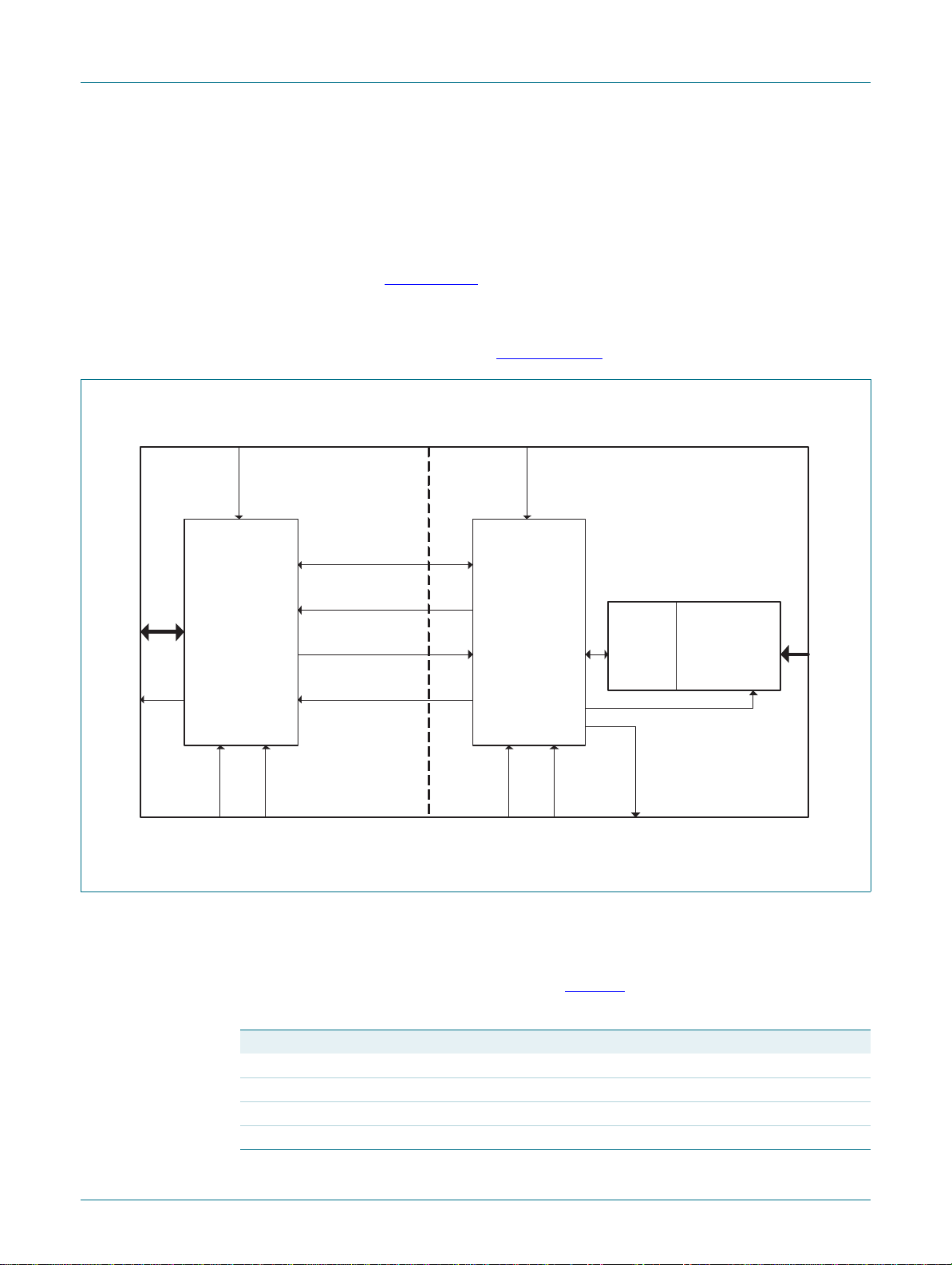
NXP Semiconductors
ADC
control
&
registers
ADC
control
&
registers
VPB
system
bus
update
Conversion data
Config data
IRQ
Start 0 Start 2 Start 1 Start 3
CLK_ADCx_VPB
(MSCSS SubSystem clock)
CLK_ADCx
(ADC clock)
(upto 4.5 MHz)
Analog
inputs
ADC1: 8
ADC2: 8
Sync_out
ADC
IRQ
3.3 V
Analog
to
Digital
convertor
Analog
mux
ADC domain
VPB SubSystem
domain
001aad331 **
The ADC clock is limited to 4.5 MHz maximum frequency and should always be lower
than or equal to the system clock frequency. To meet this constraint or to select the
desired lower sampling frequency the clock generation unit provides a programmable
fractional system-clock divider dedicated to the ADC clock. Conversion rate is determined
by the ADC clock frequency divided by the number of resolution bits plus one. Accessing
ADC registers requires an enabled ADC clock, which is controllable via the clock
generation unit, see Section 8.8.4
Each ADC has four start inputs. Note that start 0 and start 2 are captured in the system
clock domain while start 1 and start 3 are captured in the ADC domain. The start inputs
are connected at MSCSS level, see Section 8.7.2.1
DRAFT
ARM9 microcontroller with CAN and LIN
D
RAFT DRAFT DRAFT DRAFT DRAFT D
D
LPC2917/19
RAFT DRA
D
RAFT
DR
DRAFT
F
T DRAFT DRAFT DRAFT DRA
AFT
DRA
DR
AFT
DRAFT
DR
F
T DRAF
.
for details.
Fig 9. ADC block diagram
8.7.5.3 ADC pin description
The two ADC modules in the MSCSS have the pins described below. The ADCx input
pins are combined with other functions on the port pins of the LPC2917/19. The VREFN
and VREFP pins are common for both ADCs. Table 20
LPC2917_19_1 © NXP B.V. 2007. All rights reserved.
Preliminary data sheet Rev. 1.01 — 15 November 2007 36 of 68
Table 20. Analog to digital converter pins
Symbol Direction Description
ADCn IN[7:0] in analog input for ADCn, channel 7 to channel 0 (n is 1 or 2)
ADCn_EXT_START in ADC external start-trigger input (n is 1 or 2)
VREFN in ADC LOW reference level
VREFP in ADC HIGH reference level
shows the ADC pins.
Page 37

NXP Semiconductors
8.7.5.4 ADC clock description
The ADC modules are clocked from two different sources; CLK_MSCSS_ADCx_VPB and
CLK_ADCx (x = 1 or 2), see Section 7.2.2
and CLK_MSCSS_ADCx_VPB branch clocks for power management. If an ADC is
unused both its CLK_MSCSS_ADCx_VPB and CLK_ADCx can be switched off.
The frequency of all the CLK_MSCSS_ADCx_VPB clocks is identical to
CLK_MSCSS_VPB since they are derived from the same base clock
BASE_MSCSS_CLK. Likewise the frequency of all the CLK_ADCx clocks is identical
since they are derived from the same base clock BASE_ADC_CLK.
The register interface towards the system bus is clocked by CLK_MSCSS_ADCx_VPB.
Control logic for the analog section of the ADC is clocked by CLK_ADCx, see also
Figure 9
8.7.6 PWM
DRAFT
ARM9 microcontroller with CAN and LIN
. Note that each ADC has its own CLK_ADCx
.
D
RAFT DRAFT DRAFT DRAFT DRAFT D
D
LPC2917/19
RAFT DRA
D
RAFT
F
T DRAFT DRAFT DRAFT DRA
DR
DRAFT
AFT
DRA
DR
AFT
DRAFT
DR
F
T DRAF
8.7.6.1 Overview
The MSCSS in the LPC2917/19 includes four PWM modules with the following features.
• Six pulse-width modulated output signals
• Double edge features (rising and falling edges programmed individually)
• Optional interrupt generation on match (each edge)
• Different operation modes: continuous or run-once
• 16-bit PWM counter and 16-bit prescale counter allow a large range of PWM periods
• A protective mode (TRAP) holding the output in a sof tware-contro llable st ate and with
optional interrupt generation on a trap event
• Three capture registers and capture trigger pins with optional interrupt generation on
a capture event
• Interrupt generation on match event, capture event, PWM counter overflow or trap
event
• A burst mode mixing the external carrier signal with internally generated PWM
• Programmable sync-delay output to trigger other PWM modules (master/slave
behavior)
8.7.6.2 Description
The ability to provide flexible waveforms allows PWM blocks to be used in multiple
applications; e.g. automotive dimmer/lamp control and fan control. Pulse-width
modulation is the preferred method for regulating power since no additional heat is
generated and it is energy-efficient when compared with linear-regulating voltage control
networks.
The PWM delivers the waveforms/pulses of the desired duty cycles and cycle periods. A
very basic application of these pulses can be in controlling the amount of power
transferred to a load. Since the duty cycle of the pulses can be controlled, the desired
amount of power can be transferred for a controlled duration. Two examples of such
applications are:
LPC2917_19_1 © NXP B.V. 2007. All rights reserved.
Preliminary data sheet Rev. 1.01 — 15 November 2007 37 of 68
Page 38

NXP Semiconductors
PWM
control
&
registers
PWM
Counter,
prescale
counter
&
shadow
registers
VPB system bus
update
Capture data
Config data
IRQ’s
Sync_in
Capture inputs
IRQ capt_match
PWM domain
VPB domain
IRQ pwm
Match outputs
PWM counter value
Transfer_enable_in
Transfer_enable_outSync_out
Carier inputs
Trap input
• Automotive dimmer controller: The flexibility of providing waves of a desired duty
• Motor controller: The PWM provides multi-phase outputs, an d these outputs can be
DRAFT
ARM9 microcontroller with CAN and LIN
D
RAFT DRAFT DRAFT DRAFT DRAFT D
D
LPC2917/19
RAFT DRA
D
RAFT
DR
AFT
DRAFT
DRA
F
T DRAFT DRAFT DRAFT DRA
cycle and cycle period allows the PWM to control the amount of power to be
transferred to the load. The PWM functions as a dimmer controller in this application
controlled to have a certain pattern sequence. In this way the force/torque of the
motor can be adjusted as desired. This makes the PWM function as a motor drive.
DR
AFT
DRAFT
DR
F
T DRAF
Fig 10. PWM block diagram
The PWM block diagram in Figure10 shows the basic architecture of each PWM. PWM
functionality is split into two major parts, a VPB domain and a PWM domain, both of which
run on clocks derived from the BASE_MSCSS_CLK. This split into two domains affects
behavior from a system-level perspective. The actual PWM and prescale counters are
located in the PWM domain but system control takes place in the VPB domain.
The actual PWM consists of two counters; a 16-bit prescale counter and a 16-bit PWM
counter. The position of the rising and falling edges of the PWM outputs can be
programmed individually. The prescale counter allows high system bus frequencies to be
scaled down to lower PWM periods. Registers are available to capture the PWM counter
values on external events.
Note that in the Modulation and Sampling SubSystem, each PWM has its individual clock
source CLK_MSCSS_PWMx (x runs from 0 to 3). Both the prescale and the timer
counters within each PWM run on this clock CLK_MSCSS_PWMx, and all time references
are related to the period of this clock. See Section 8.8
for information on generation of
these clocks.
8.7.6.3 Synchronizing the PWM counters
A mechanism is included to synchronize the PWM period to other PWMs by providing a
sync input and a sync output with programmable delay. Several PWMs can be
LPC2917_19_1 © NXP B.V. 2007. All rights reserved.
Preliminary data sheet Rev. 1.01 — 15 November 2007 38 of 68
synchronized using the trans_enable_in/trans_enable_out and sync_in/sync_out ports.
See Section 8.7.2.1
in the LPC2917/19. PWM 0 can be master over PWM 1; PWM 1 can be master over
PWM 2, etc.
for details of the connections of the PWM m odules within the MSCSS
Page 39

NXP Semiconductors
8.7.6.4 Master and slave mode
A PWM module can provide synchronization signals to other modules (also called Ma ster
mode). The signal sync_out is a pulse of one clock cycle generated when the internal
PWM counter (re)starts. The sign al trans_enable_ou t is a pulse synchronous to sync_out,
generated if a transfer from system registers to PWM shadow register s occurred when the
PWM counter restarted. A delay may be inserted between the counter start and
generation of trans_enable_out and sync_out.
A PWM module can use input signals trans_enable_in and sync_in to synchronize its
internal PWM counter and the transfer of shadow registers (Slave mode).
8.7.6.5 PWM pin description
Each of the four PWM modules in the MSCSS has the following pins. These are combined
with other functions on the port pins of the LPC2917/19. Table 21
PWM3 pins.
Table 21. PWM pins
Symbol Direction Description
PWMn CAP[0] in PWM n capture input 0
PWMn CAP[1] in PWM n capture input 1
PWMn CAP[2] in PWM n capture input 2
PWMn MAT[0] out PWM n match output 0
PWMn MAT[1] out PWM n match output 1
PWMn MAT[2] out PWM n match output 2
PWMn MAT[3] out PWM n match output 3
PWMn MAT[4] out PWM n match output 4
PWMn MAT[5] out PWM n match output 5
PWMn TRAP in PWM n trap input
DRAFT
ARM9 microcontroller with CAN and LIN
D
RAFT DRAFT DRAFT DRAFT DRAFT D
D
LPC2917/19
RAFT DRA
D
RAFT
DR
AFT
DRAFT
DRA
F
T DRAFT DRAFT DRAFT DRA
shows the PWM0 to
DR
AFT
DRAFT
DR
F
T DRAF
8.7.6.6 PWM clock description
The PWM modules are clocked by CLK_MSCSS_PWMx (x = 0-3), see Section 7.2.2
.
Note that each PWM has its own CLK_MSCSS_PWMx branch clock for power
management. The frequency of all these clocks is identical to CLK_MSCSS_VPB since
they are derived from the same base clock BASE_MSCSS_CLK.
Also note that unlike the timer modules in the Peripheral SubSystem, the actual timer
counter registers of the PWM modules run at the same clock as the VPB system interface
CLK_MSCSS_VPB. This clock is independent of the AHB system clock.
If a PWM module is not used its CLK_MSCSS_PWMx branch clock can be switched off.
8.7.7 Timers in the MSCSS
8.7.7.1 Overview
The two timers in the MSCSS are functionally identical to the timers in the peripheral
subsystem, see Section 8.4.3
the timers in the peripheral subsystem, but the capture inputs and match outputs are not
available on the device pins. These signals are instead connected to the ADC and PWM
modules as outlined in the description of the MSCSS, see Section 8.7.2
LPC2917_19_1 © NXP B.V. 2007. All rights reserved.
Preliminary data sheet Rev. 1.01 — 15 November 2007 39 of 68
. The features of the timers in the MSCSS are the same as
.
Page 40

NXP Semiconductors
8.7.7.2 Description
See section Section 8.4.3.2
8.7.7.3 MSCSS timer-pin description
MSCSS timer 0 has no external pins.
MSCSS timer 1 has a PAUSE pin available as external pin. The PAUSE pin is combined
with other functions on the port pins of the LPC2917/19. Table 22
timer 1 external pin.
Table 22. MSCSS timer 1 pin
Symbol Direction Description
MSCSS PAUSE in pause pin for MSCSS timer 1
8.7.7.4 MSCSS timer-clock description
The Timer modules in the MSCSS are clocked by CLK_MSCSS_MTMRx (x = 0-1), see
Section 7.2.2
power management. The frequency of all these clocks is identical to CLK_MSCSS_VPB
since they are derived from the same base clock BASE_MSCSS_CLK.
DRAFT
ARM9 microcontroller with CAN and LIN
D
RAFT DRAFT DRAFT DRAFT DRAFT D
D
LPC2917/19
RAFT DRA
D
RAFT
DR
AFT
DRAFT
DRA
F
T DRAFT DRAFT DRAFT DRA
for a description of the timers.
shows the MSCSS
. Note that each timer has its own CLK_MSCSS_MTMRx branch clock for
DR
AFT
DRAFT
DR
F
T DRAF
Note that, unlike the timer modules in the Peripheral SubSystem, the actual timer counter
registers run at the same clock as the VPB system interface CLK_MSCSS_VPB. This
clock is independent of the AHB system clock.
If a timer module is not used its CLK_MSCSS_MTMRx branch clock can be switched off.
8.8 Power, clock and reset control subsystem
8.8.1 Overview
The Power, Clock and Reset Control Subsystem (PCRSS) in the LPC2917/19 includes a
Clock Generator Unit (CGU), a Reset Generator Unit (RGU) and a Power Man a ge m ent
Unit (PMU).
8.8.2 Description
Figure 11 provides an overview of the PCRSS. An AHB-to-DTL bridge takes care of
communication with the AHB system bus.
LPC2917_19_1 © NXP B.V. 2007. All rights reserved.
Preliminary data sheet Rev. 1.01 — 15 November 2007 40 of 68
Page 41

NXP Semiconductors
Power, Clock & Reset
RGU
CGU
RGU
registers
Input Deglitch/
Sync
POR
Reset Output
Delay Logic
branch
clocks
FDIV[6:0]
PLL
out0
out1
…
out9
Low Power
Ring Oscillator
(Ringo)
base
clocks
PMU
Clock
Gates
wakeup_a
AHB Master
Disable Grant
AHB Master
Disable Req
WARM_RST
COLD_RST
PCR_RST
RGU_RST
POR_RST
PMU _reg
Clock Ena ble
Control
RSTN (device pin)
Reset from Watchdog counter
AHB_RST
...
...
SCU_RST
AHB2DTL
Bridge
CGU
registers
Xtal Oscillator
xo 50m _out
xo50m_in
DRAFT
ARM9 microcontroller with CAN and LIN
D
RAFT DRAFT DRAFT DRAFT DRAFT D
D
LPC2917/19
RAFT DRA
D
RAFT
DR
AFT
DRAFT
DRA
F
T DRAFT DRAFT DRAFT DRA
DR
AFT
DRAFT
DR
F
T DRAF
Fig 11. PCRSS block diagram
8.8.3 PCR subsystem clock description
The PCRSS is clocked by a number of different clocks. CLK_SYS_PCRSS clocks the
AHB side of the AHB to DTL bus bridge and CLK_PCR_SLOW clocks the CGU, RGU and
PMU internal logic, see Section 7.2.2
BASE_SYS_CLK, which can be switched off in low-power modes. CLK_PCR_SLOW is
derived from BASE_PCR_CLK and is always on in order to be able to wake up from
low-power modes.
8.8.4 Clock Generation Unit (CGU)
. CLK_SYS_PCRSS is derived from
8.8.4.1 Overview
The key features are:
LPC2917_19_1 © NXP B.V. 2007. All rights reserved.
Preliminary data sheet Rev. 1.01 — 15 November 2007 41 of 68
Page 42

NXP Semiconductors
• Generation of 10 and 2 test-base clocks, selectable from several embedd ed clock
• Crystal oscillator with power-down
• Control PLL with power-down
• Very low-power ring oscillator, always on to provide a ’safe clock’
• Seven fractional clock dividers with L/D division
• Individual source selector for each base clock, with glitch-free switching
• Autonomous clock-activity detection on every clock source
• Protection against switching to invalid or inactive clock sources
• Embedded frequency counter
• Register write-protection mechanism to prevent unintentional alteration of clocks
Remark: Any clock-frequency adjustment has a direct impact on the timing of on- boar d
peripherals such as the UARTs, SPI, watchdog, timers, CAN controller, LIN master
controller, ADCs or flash-memory interface.
sources
DRAFT
ARM9 microcontroller with CAN and LIN
D
RAFT DRAFT DRAFT DRAFT DRAFT D
D
LPC2917/19
RAFT DRA
D
RAFT
DR
AFT
DRAFT
DRA
F
T DRAFT DRAFT DRAFT DRA
DR
AFT
DRAFT
DR
F
T DRAF
8.8.4.2 Description
The clock generation unit provides 10 internal clock sources as described in Table 23
T able 23. CGU base clocks
Number Name Frequency
0 BASE_SAFE_CLK 0.4 Base safe clock (always on)
1 BASE_SYS_CLK 80 Base system clock
2 BASE_PCR_CLK 0.4
3 BASE_IVNSS_CLK 80 Base IVNSS subsystem clock
4 BASE_MSCSS_CLK 80 Base MSCSS subsystem clock
5 BASE_UART_CLK 80 Base UART clock
6 BASE_SPI_CLK 40 Base SPI clock
7 BASE_TMR_CLK 80 Base timers clock
8 BASE_ADC_CLK 4.5 Base ADCs clock
[1] Maximum frequency that guarantees stable operation of the LPC2917/19.
[2] Fixed to low-power oscillator.
For generation of these base clocks, the CGU consists of primary and secondary clock
generators and one output generator for each base clock.
(MHz)
[2]
.
Description
[1]
Base PCR subsystem clock
LPC2917_19_1 © NXP B.V. 2007. All rights reserved.
Preliminary data sheet Rev. 1.01 — 15 November 2007 42 of 68
Page 43

NXP Semiconductors
LP_OSC
Xtal
Oscilator
PLL
Clock Source Bus
Frequency
Monitor
Clock
Detection
DTL MMIO Interface
FDIV0
FDIV1
FDIV6
OUT 0
OUT 1
OUT 9
DRAFT
ARM9 microcontroller with CAN and LIN
D
RAFT DRAFT DRAFT DRAFT DRAFT D
D
LPC2917/19
RAFT DRA
D
RAFT
DR
AFT
DRAFT
DRA
F
T DRAFT DRAFT DRAFT DRA
DR
AFT
DRAFT
DR
F
T DRAF
Fig 12. Block diagram of the CGU
There are two primary clock generators: a low-power ring oscillator (LP_OSC) and a
crystal oscillator. See Figure 12
LP_OSC is the source for the BASE_PCR_CLK that clocks the CGU itself and for
BASE_SAFE_CLK that clocks a minimum of other logic in the device (like the watchdog
.
timer). To prevent the device from losing its clock source LP_OSC cannot be put into
power-down. The crystal oscillator can be used as source for high-frequency clocks or as
an external clock input if a crystal is not connected.
Secondary clock generators are a PLL and seven fractional dividers (FDIV0..6). The PLL
has three clock outputs: normal, 120° phase-shifted and 240° phase-shifted.
Configuration of the CGU: For every output generator - generating the base clocks - a
choice can be made from the primary and secondary clock generators according to
Figure 13
LPC2917_19_1 © NXP B.V. 2007. All rights reserved.
Preliminary data sheet Rev. 1.01 — 15 November 2007 43 of 68
.
Page 44

NXP Semiconductors
PLL160M
FDIV0..6
XO50M
OSC1M
Clock
outputs
clkout /
clkout120 /
clkout240
Output
Control
DRAFT
ARM9 microcontroller with CAN and LIN
D
RAFT DRAFT DRAFT DRAFT DRAFT D
D
LPC2917/19
RAFT DRA
D
RAFT
DR
AFT
DRAFT
DRA
F
T DRAFT DRAFT DRAFT DRA
DR
AFT
DRAFT
DR
F
T DRAF
Fig 13. Structure of the clock generation scheme
Any output generator (except for BASE_SAFE_CLK and BASE_PCR_CLK) can be
connected to either a fractional divider (FDIV0..6) or to one of the outputs of the PLL or to
LP_OSC/crystal oscillator directly . BASE_SAFE_CLK and BASE_PCR_CLK can use only
LP_OSC as source.
The fractional dividers can be connected to one of the outputs of the PLL or directly to
LP_OSC/crystal Oscillator.
The PLL can be connected to the crystal oscillator.
In this way every output generating the base clocks can be configured to get the required
clock. Multiple output generators can be connected to the same primary or secondary
clock source, and multiple secondary clock sources can be connected to the same PLL
output or primary clock source.
Invalid selections/programming - connecting the PLL to an FDIV or to one of the PLL
outputs itself for example - will be blocked by hardware. The control register will not be
written, the previous value will be kept, although all other fields will be written with new
data. This prevents clocks being blocked by incorrect programming.
Default Clock Sources: Every secondary clock generator or output generator is
connected to LP_OSC at reset. In this way the device runs at a low frequency after reset.
It is recommended to switch BASE_SYS_CLK to a high-frequency clock generator as
(one of) the first step(s) in the boot code after verifying that the high-frequency clock
generator is running.
LPC2917_19_1 © NXP B.V. 2007. All rights reserved.
Preliminary data sheet Rev. 1.01 — 15 November 2007 44 of 68
Page 45

NXP Semiconductors
Clock Activity Detection: Clocks that are inactive are automatically regarded as invalid,
and values of ’CLK_SEL ’ that would select those clocks are masked and not written to the
control registers. This is accomplished by adding a clock detector to every clock
generator . The RDET register keep s track of which clocks ar e active and inactive, and the
appropriate ‘CLK_SEL’ values are masked and unmasked accordingly. Each clock
detector can also generate interrupts at clock activation and deactivation so that the
system can be notified of a change in internal clock status.
Clock detection is done using a counter running at the BASE_PCR_CLK frequency. If no
positive clock edge occurs before the counter has 32 cycles of BASE_PCR_CLK the clock
is assumed to be inactive. As BASE_PCR_CLK is slower than any of the clocks to be
detected, normally only one BASE_PCR_CLK cycle is needed to detect activity. After
reset all clocks are assumed to be ‘non-present’, so the RDET status register will be
correct only after 32 BASE_PCR_CLK cycles.
Note that this mechanism cannot protect against a currently-selected clock going from
active to inactive state. Therefore an inactive clock may still be sent to the system under
special circumstances, although an interrupt can still be generated to notify the system.
DRAFT
ARM9 microcontroller with CAN and LIN
D
RAFT DRAFT DRAFT DRAFT DRAFT D
D
LPC2917/19
RAFT DRA
D
RAFT
F
T DRAFT DRAFT DRAFT DRA
DR
AFT
DRAFT
DRA
DR
AFT
DRAFT
DR
F
T DRAF
Glitch-Free Switching: Provisions are included in the CGU to allow clocks to be
switched glitch-free, both at the output generator stage and also at secondary source
generators.
In the case of the PLL the clock will be stopped and held low for long enough to allow the
PLL to stabilize and lock before being re-enabled. For all non-PLL Generators the switch
will occur as quickly as possible, although there will always be a period when the clock is
held low due to synchronization requirements.
If the current clock is high and does not go low within 32 cycles of BASE_PCR_CLK it is
assumed to be inactive and is asynchronously forced low. This prevents deadlocks on the
interface.
8.8.4.3 PLL functional description
A block diagram of the PLL is shown in Figure 14
analog section. This block compares the ph ase and frequency of the input s and generates
the main clock
to create the output clock, or sent directly to the output. The main output clock is then
divided by M by the programmable feedback divider to generate the feedback clock. The
output signal of the analog section is also moni to re d by th e loc k det ec to r to sign a l when
the PLL has locked onto the input clock.
2
. These clocks are either divided by 2 *P by th e pro grammable post divider
. The input clock is fed directly to the
2. Generation of the main clock is restricted by the frequency range of the PLL clock input. See Table31, Dynamic characteristics.
LPC2917_19_1 © NXP B.V. 2007. All rights reserved.
Preliminary data sheet Rev. 1.01 — 15 November 2007 45 of 68
Page 46

NXP Semiconductors
P23CCO
/ MDIV
clkout120 /
clkout240
/ 2PDIV
MSEL
PSEL
P23EN
Input clock
Bypass
Direct
clkout
Fig 14. PLL block diagram
Triple output phases
DRAFT
ARM9 microcontroller with CAN and LIN
D
RAFT DRAFT DRAFT DRAFT DRAFT D
D
LPC2917/19
RAFT DRA
D
RAFT
DR
AFT
DRAFT
DRA
F
T DRAFT DRAFT DRAFT DRA
DR
AFT
DRAFT
DR
F
T DRAF
For applications that require multiple clock phases two additional clock outputs can be
enabled by setting register P23EN to ’1’, thus giving three clocks with a 120° phase
difference. In this mode all three clocks generated by the analog section are sent to the
output dividers. When the PLL has not yet achieved lock the second and third phase
output dividers run unsynchronized, which means that the phase relation of the output
clocks is unknown. When the PLL LOCK register is set the second and third phase of the
output dividers are synchronized to the main output clock CLKOUT PLL, thus giving three
clocks with a 120° phase difference.
Direct output mode
In normal operating mode (with DIRECT set to ’0’) the CCO clock is divided by 2, 4, 8 or
16 depending on the value on the PSEL[1:0] input, giving an output clock with a 50% duty
cycle. If a higher output frequency is needed the CCO clock can be sent directly to the
output by setting DIRECT to ’1’. Since the CCO does not directly generate a 50% duty
cycle clock, the output clock duty cycle in this mode can deviate from 50%.
Power-down control
A power-down mode has been incorporated to reduce power consumption when the PLL
clock is not needed. This is enabled by setting the PD control register bit. In this mo de the
analog section of the PLL is turned off, the oscillator and the phase-frequency detector are
stopped and the dividers enter a reset state. While in power-down mod e the LOCK output
is low, indicating that the PLL is not in lock. When power-down mode is terminated by
clearing the PD control-register bit the PLL resumes normal operation, and makes the
LOCK signal high once it has regained lock on the input clock.
8.8.4.4 CGU pin description
The CGU module in the LPC2917/19 has the pins listed in Table 24
Table 24. CGU pins
Symbol Direction Description
XOUT_OSC out Oscillator crystal output
LPC2917_19_1 © NXP B.V. 2007. All rights reserved.
Preliminary data sheet Rev. 1.01 — 15 November 2007 46 of 68
XIN_OSC in Oscillator crystal input or external clock input
below.
Page 47

DRAFT
NXP Semiconductors
ARM9 microcontroller with CAN and LIN
D
RAFT DRAFT DRAFT DRAFT DRAFT D
D
LPC2917/19
RAFT DRA
D
RAFT
DR
AFT
DRAFT
DRA
F
T DRAFT DRAFT DRAFT DRA
8.8.5 Reset Generation Unit (RGU)
8.8.5.1 Overview
The key features of the Reset Generation Unit (RGU) are:
• Reset controlled individually per subsystem
• Automatic reset stretching and release
• Monitor function to trace resets back to source
• Register write-protection mechanism to prevent unintentional resets
8.8.5.2 Description
The RGU controls all internal resets.
Each reset output is defined as a (combination of) reset input sources including the
external reset input pins and internal power -o n rese t, see Table 25
listed in this table form a sort of cascade to provide the multiple levels of impact that a
reset may have. The combined input sources are logically OR-ed together so that
activating any of the listed reset sources causes the output to go active.
Table 25. Reset output configuration
Reset Output Reset Source parts of the device reset when activated
POR_RST power-on reset module LP_OSC; is source for RGU_RST
RGU_RST POR_RST, RSTN pin RGU internal; is source for PCR_RST
PCR_RST RGU_R ST, WATCHDOG PCR internal; is source for COLD_RST
COLD_RST PCR_RST parts with COLD_RST as reset source below
WARM_RST COLD_RST parts with WARM_RST as reset source below
SCU_RST COLD_RST SCU
CFID_RST COLD_RST CFID
FMC_RST COLD_RST embedded Flash-Memory Controller (FMC)
EMC_RST COLD_RST embedded SRAM-Memory Controller
SMC_RST COLD_ RST external Static-Memory Controller (SMC)
GESS_A2V_RST WARM_RST GeSS AHB-to-VPB bridge
PESS_A2V_RST WARM_RST PeSS AHB-to-VPB bridge
GPIO_RST WARM_RST all GPIO modules
UART_RST WARM_RST all UART modules
TMR_RST WARM_RST all Timer modules in PeSS
SPI_RST WARM_RST all SPI modules
IVNSS_A2V_RST WARM_RST IVNSS AHB-to-VPB bridge
IVNSS_CAN_RST WARM_RST all CAN modules including Acceptance filter
IVNSS_LIN_RST WARM_RST all LIN modules
MSCSS_A2V_RST WARM_RST MSCSS AHB to VPB bridge
MSCSS_PWM_RST WARM_RST all PWM modules
MSCSS_ADC_RST WARM_RST all ADC modules
MSCSS_TMR_RST WARM_RST all Timer modules in MSCSS
VIC_RST WARM_RST Vectored Interrupt Controller (VIC)
AHB_RST WARM_RST CPU and AHB Multilayer Bus infrastructure
LPC2917_19_1 © NXP B.V. 2007. All rights reserved.
Preliminary data sheet Rev. 1.01 — 15 November 2007 47 of 68
. The first five resets
DR
AFT
DRAFT
DR
F
T DRAF
Page 48

NXP Semiconductors
8.8.5.3 RGU pin description
The RGU module in the LPC2917/19 has the following pins. Table 26
pins.
Table 26. RGU pins
Symbol DirectionDescription
RSTN IN external reset input, Active LOW; pulled up internally
8.8.6 Power Management Unit (PMU)
8.8.6.1 Overview
This module enables software to actively control the system’s power consumption by
disabling clocks not required in a particular operating mo de .
Using the base clocks from the CGU as input, the PMU generates branch clocks to the
rest of the LPC2917/19. Output clocks branched from the same base clock are phaseand frequency-related. These branch clocks can be individually controlled by software
programming.
DRAFT
ARM9 microcontroller with CAN and LIN
D
RAFT DRAFT DRAFT DRAFT DRAFT D
D
LPC2917/19
RAFT DRA
D
RAFT
F
T DRAFT DRAFT DRAFT DRA
shows the RGU
DR
AFT
DRAFT
DRA
DR
AFT
DRAFT
DR
F
T DRAF
The key features are:
• Individual clock control for all LPC2917/19 sub-modules
• Activates sleeping clocks when a wake-up event is detected
• Clocks can be individually disabled by software
• Supports AHB master-disable protocol when AUTO mode is set
• Disables wake-up of enabled clocks when power-down mode is set
• Activates wake-up of enabled clocks when a wake-up event is received
• Status r egister is available to indicate if an input base clock can be safely switch ed of f
(i.e. all branch clocks are disabled)
8.8.6.2 Description
The PMU controls all internal clocks of the device for power-mode management. With
some exceptions, each branch clock can be switched on or of f individually under control of
software register bits located in its individual configuration register. Some branch clocks
controlling vital parts of the device operate in a fixed mode. Table 27
control bits are supported by each branch clock.
By programming the configuration register the user can control which clocks are switched
on or off, and which clocks are switched off when entering power-down mode.
Note that the standby-wait-for-interrupt instructions of the ARM968E- S pr ocessor (p utting
the ARM CPU into a low-power state) are not supported. Instead putting the ARM CPU
into power-down should be controlled by disabling the branch clock for the CPU.
shows which mode-
Remark: For any disabled branch clocks to be re-activated their corresponding base
clocks must be running (controlled by the CGU).
Table 27
Every branch clock is related to one particular base clock: it is not possible to switch the
source of a branch clock in the PMU.
LPC2917_19_1 © NXP B.V. 2007. All rights reserved.
Preliminary data sheet Rev. 1.01 — 15 November 2007 48 of 68
shows the relation between branch and base clocks, see also Section 7.2.1.
Page 49

NXP Semiconductors
Table 27. Branch clock overview
Legend:
"1" Indicates that the related register bit is tied off to logic HIGH, all writes are ignored
"0" Indicates that the related register bit is tied off to logic LOW, all writes are ignored
“+” Indicates that the related register bit is readable and writable
Branch Clock Name Base Clock Implemented Switch On/Off
CLK_SAFE BASE_SAFE_CLK 0 0 1
CLK_SYS_CPU BASE_SYS_CLK + + 1
CLK_SYS BASE_SYS_CLK + + 1
CLK_SYS_PCR BASE_SYS_CLK + + 1
CLK_SYS_FMC BASE_SYS_CLK + + +
CLK_SYS_RAM0 BASE_SYS_CLK + + +
CLK_SYS_RAM1 BASE_SYS_CLK + + +
CLK_SYS_SMC BASE_SYS_CLK + + +
CLK_SYS_GESS BASE_SYS_CLK + + +
CLK_SYS_VIC BASE_SYS_CLK + + +
CLK_SYS_PESS BASE_SYS_CLK + + +
CLK_SYS_GPIO0 BASE_SYS_CLK + + +
CLK_SYS_GPIO1 BASE_SYS_CLK + + +
CLK_SYS_GPIO2 BASE_SYS_CLK + + +
CLK_SYS_GPIO3 BASE_SYS_CLK + + +
CLK_SYS_IVNSS_A BASE_SYS_CLK + + +
CLK_SYS_MSCSS_A BASE_SYS_CLK + + +
CLK_SYS_CHCA BASE_SYS_CLK + + +
CLK_SYS_CHCB BASE_SYS_CLK + + +
CLK_PCR_SLOW BASE_PCR_CLK + + 1
CLK_IVNSS_VPB BASE_IVNSS_CLK + + +
CLK_IVNSS_CANC0 BASE_IVNSS_CLK + + +
CLK_IVNSS_CANC1 BASE_IVNSS_CLK + + +
CLK_IVNSS_LIN0 BASE_IVNSS_CLK + + +
CLK_IVNSS_LIN1 BASE_IVNSS_CLK + + +
CLK_MSCSS_VPB BASE_MSCSS_CLK + + +
CLK_MSCSS_MTMR0 BASE_MSCSS_CLK + + +
CLK_MSCSS_MTMR1 BASE_MSCSS_CLK + + +
CLK_MSCSS_PWM0 BASE_MSCSS_CLK + + +
CLK_MSCSS_PWM1 BASE_MSCSS_CLK + + +
CLK_MSCSS_PWM2 BASE_MSCSS_CLK + + +
CLK_MSCSS_PWM3 BASE_MSCSS_CLK + + +
CLK_MSCSS_ADC1_VPB BASE_MSCSS_CLK + + +
CLK_MSCSS_ADC2_VPB BASE_MSCSS_CLK + + +
CLK_UART0 BASE_UART_CLK + + +
CLK_UART1 BASE_UART_CLK + + +
DRAFT
ARM9 microcontroller with CAN and LIN
Mechanism
WAKEUP AUTO RUN
D
RAFT DRAFT DRAFT DRAFT DRAFT D
D
LPC2917/19
RAFT DRA
D
RAFT
DR
AFT
DRAFT
DRA
F
T DRAFT DRAFT DRAFT DRA
DR
AFT
DRAFT
DR
F
T DRAF
LPC2917_19_1 © NXP B.V. 2007. All rights reserved.
Preliminary data sheet Rev. 1.01 — 15 November 2007 49 of 68
Page 50

NXP Semiconductors
Table 27. Branch clock overview
Legend:
"1" Indicates that the related register bit is tied off to logic HIGH, all writes are ignored
"0" Indicates that the related register bit is tied off to logic LOW, all writes are ignored
“+” Indicates that the related register bit is readable and writable
Branch Clock Name Base Clock Implemented Switch On/Off
CLK_SPI0 BASE_SPI_CLK + + +
CLK_SPI1 BASE_SPI_CLK + + +
CLK_SPI2 BASE_SPI_CLK + + +
CLK_TMR0 BASE_TMR_CLK + + +
CLK_TMR1 BASE_TMR_CLK + + +
CLK_TMR2 BASE_TMR_CLK + + +
CLK_TMR3 BASE_TMR_CLK + + +
CLK_ADC1 BASE_ADC_CLK + + +
CLK_ADC2 BASE_ADC_CLK + + +
CLK_TESTSHELL_IP BASE_CLK_TESTSHELL 0 0 1
…continued
DRAFT
ARM9 microcontroller with CAN and LIN
Mechanism
WAKEUP AUTO RUN
D
RAFT DRAFT DRAFT DRAFT DRAFT D
D
LPC2917/19
RAFT DRA
D
RAFT
F
T DRAFT DRAFT DRAFT DRA
DR
AFT
DRAFT
DRA
DR
AFT
DRAFT
DR
F
T DRAF
8.8.6.3 PMU pin description
The PMU has no external pins.
8.9 Vectored interrupt controller
8.9.1 Overview
The LPC2917/19 contains a very flexible and powerful Vectored Interrupt Controller (VIC)
to interrupt the ARM processor on request.
The key features are:
• Level-active interrupt request with programmable polarity
• 56 interrupt-request inputs
• Software-interrupt request capability associated with each request input
• Observability of interrupt-request state before masking
• Software-programmable priority assignments to interrupt requests up to 15 levels
• Software-programmable routing of interrupt requests towards the ARM-processor
inputs IRQ and FIQ
• Fast identification of interrupt requests through vector
• Support for nesting of interrupt service routines
8.9.2 Description
The Vectored Inter rupt Controller routes incoming interrupt requests to the ARM
processor. The interrupt target is configured for each interrupt request input of the VIC.
The targets are defined as follows:
• Target 0 is ARM processor FIQ (fast interrupt service)
• Target 1 is ARM processor IRQ (standard interrupt service)
LPC2917_19_1 © NXP B.V. 2007. All rights reserved.
Preliminary data sheet Rev. 1.01 — 15 November 2007 50 of 68
Page 51

NXP Semiconductors
Interrupt-request masking is perfor me d indiv idually per interrupt target by comparing the
priority level assigned to a specific interrupt request with a target-specific priority
threshold. The priority levels are defined as follows:
• Priority level 0 corresponds to ‘masked’ (i.e. interrupt requests with priority 0 never
• Priority 1 corresponds to the lowest priority
• Priority 15 corresponds to the highest priority
Software interrupt support is provided and can be supplied for:
• Testing RTOS interrupt handling without using device-specific interrupt service
• Software emulation of an interrupt-requesting device, including interrupts
8.9.3 VIC pin description
The VIC module in the LPC2917/19 has no external pins.
lead to an interrupt)
routines
DRAFT
ARM9 microcontroller with CAN and LIN
D
RAFT DRAFT DRAFT DRAFT DRAFT D
D
LPC2917/19
RAFT DRA
D
RAFT
DR
AFT
DRAFT
DRA
F
T DRAFT DRAFT DRAFT DRA
DR
AFT
DRAFT
DR
F
T DRAF
8.9.4 VIC clock description
The VIC is clocked by CLK_SYS_VIC, see Section 7.2.2.
9. Limiting values
Table 28. Limiting values
In accordance with the Absolute Maximum Rating System (IEC 60134).
Symbol Parameter Conditions Min Max Unit
Supply pins
P
tot
V
DD(CORE)
V
DD(OSC_PLL)
V
DD(ADC3V3)
V
DD(IO)
I
DD
I
SS
Input pins and I/O pins
V
XIN_OSC
V
XIN_RTC
V
I(IO)
V
I(ADC)
V
VREFP
V
VREFN
I
I(ADC)
Output pins and I/O pins configured as output
Total power dissipation.
Core supply voltage. −0.5 +2.0 V
Oscillator and PLL supply
voltage.
3.3 V ADC supply voltage. −0.5 +4.6 V
I/O digital supply voltage. −0.5 +4.6 V
Supply current. Average value per supply
Ground current. Average value per ground
Voltage on pin XIN_OSC. −0.5 +2.0 V
Voltage on pin XIN_RTC. −0.5 +2.0 V
I/O input voltage.
ADC input voltage. I/O port 0.
Voltage on pin VREFP. −0.5 +3.6 V
Voltage on pin VREFN. −0.5 +3.6 V
ADC input current. Average value per input pin.
[1]
-1 W
−0.5 +2.0 V
[2]
-98 mA
pin.
[2]
-98 mA
pin.
[3][4][5]
−0.5 V
[4][5]
−0.5 V
[2]
-35 mA
+3.0 V
DD(IO)
DD(ADC3V3)
+0.5 V
LPC2917_19_1 © NXP B.V. 2007. All rights reserved.
Preliminary data sheet Rev. 1.01 — 15 November 2007 51 of 68
Page 52

DRAFT
NXP Semiconductors
D
RAFT DRAFT DRAFT DRAFT DRAFT D
D
LPC2917/19
RAFT DRA
D
RAFT
DR
DRAFT
ARM9 microcontroller with CAN and LIN
F
T DRAFT DRAFT DRAFT DRA
Table 28. Limiting values
In accordance with the Absolute Maximum Rating System (IEC 60134).
Symbol Parameter Conditions Min Max Unit
I
OHS
HIGH-state short-circuit
output current.
I
OLS
LOW-state short-circuit
output current.
General
T
T
T
stg
amb
vj
Storage temperature. −40 +150 °C
Ambient temperature. −40 +85 °C
Virtual junction temperature.
Memory
n
endu(fl)
t
ret(fl)
Endurance of flash memory. - 100000 cycle
Flash memory retention
time.
Electrostatic discharge
V
esd
Electrostatic discharge
voltage.
…continued
Drive HIGH, output shorted
[9]
- −33 mA
to VSS(IO).
Drive LOW, output shorted
[9]
-+38 mA
to VDD(IO).
[6]
−40 +125 °C
-20 year
On all pins.
[7]
Human body model.
Machine model.
−2000 +2000 V
[8]
−200 +200 V
Charged device model. −500 +500 V
On corner pins.
Charged device model. -750 +750 V
AFT
DRA
DR
AFT
DRAFT
DR
F
T DRAF
[1] Based on package heat transfer, not device power consumption.
[2] Peak current must be limited at 25 times average current.
[3] For I/O Port 0, the maximum input voltage is defined by V
[4] Only when V
[5] Note that pull-up should be off. With pull-up do not exceed 3.6 V.
[6] In accordance with IEC 60747-1. An alternative definition of the virtual junction temperature is: T
a fixed value; see Section 10
[7] Human-body model: discharging a 100 pF capacitor via a 10 kΩ series resistor.
[8] Machine model: discharging a 200 pF capacitor via a 0.75 μH series inductance and 10 Ω resistor.
[9] 112 mA per V
DD(IO)
DD(IO)
is present.
or V
SS(IO)
. The rating for Tvj limits the allowable combinations of power dissipation and ambient temperature.
should not be exceeded.
I(ADC)
.
vj=Tamb+Ptot
10. Thermal characteristics
Table 29. Thermal characteristics
Symbol Parameter Conditions Value Unit
R
th(j-a)
thermal resistance from
junction to ambient
in free air
package;
LQFP144 62 K/W
× R
th(j-a)
where R
th(j-a)
is
LPC2917_19_1 © NXP B.V. 2007. All rights reserved.
Preliminary data sheet Rev. 1.01 — 15 November 2007 52 of 68
Page 53

NXP Semiconductors
11 . Static characteristics
DRAFT
ARM9 microcontroller with CAN and LIN
D
RAFT DRAFT DRAFT DRAFT DRAFT D
D
LPC2917/19
RAFT DRA
D
RAFT
DR
AFT
DRAFT
DRA
F
T DRAFT DRAFT DRAFT DRA
DR
AFT
DRAFT
DR
F
T DRAF
Table 30. Static characteristics
V
DD(CORE)=VDD(OSC_PLL)
measured with respect to ground; positive currents flow into the IC; unless otherwise specified.
; V
= 2.7 V to 3.6 V; V
DD(IO)
DD(A3V3)
= 3.0 V to 3.6 V; Tvj=-40°Cto+125°C; all voltages are
[1]
Symbol Parameter Conditions Min Typ Max Unit
Supplies
Core supply
V
DD(CORE)
I
DDD(CORE)
Core supply voltage. 1.71 1.80 1.89 V
Core supply current. ARM9 and all
-1.12.5mA/
peripherals active at
MHz
max clock speeds.
[2]
All clocks off.
-30450μA
I/O supply
V
DD(IO)
I/O digital supply voltage. 2.7 - 3.6 V
Oscillator supply
V
DD(OSC_PLL)
Oscillator and PLL supply
1.71 1.80 1.89 V
voltage.
I
DDD(OSC_PLL)
Oscillator and PLL supply
current.
start-up 1.5 - 3 mA
Normal mode - - 1 mA
Power-down mode - - 2 μA
Analog-to-digital converter supply
V
DD(A3V3)
I
DDA(A3V3)
3.3 V ADC supply voltage 3.0 3.3 3.6 V
3.3 V ADC analog supply
current.
Normal mode - - 1.9 mA
Power-down mode - - 4 μA
Input pins and I/O pins configured as input
V
I
Input voltage. All port pins and V
DD(IO)
[7][8]
-0.5 - + 5.5 V
applied except port 0
pins 16 to 31.
see Section 9
Port 0 pins 16 to 31.
All port pins and V
DD(IO)
[8]
-0.5 - +3.6 V
V
VREFP
not applied.
All other I/O pins,
-0.5 - VDD(IO) V
RESET_N, TRST_N,
TDI, JTAGSEL, TMS,
TCK.
V
IH
HIGH-state input voltage. All port pins, RESET_N,
2.0 - - V
TRST_N, TDI,
JTAGSEL, TMS, TCK.
V
IL
LOW-state input voltage. All port pins, RESET_N,
--0.8V
TRST_N, TDI,
JTAGSEL, TMS, TCK.
V
hys
I
LIH
Hysteresis voltage. 0.4 - - V
HIGH-state input leakage
--1μA
current.
LPC2917_19_1 © NXP B.V. 2007. All rights reserved.
Preliminary data sheet Rev. 1.01 — 15 November 2007 53 of 68
Page 54

DRAFT
NXP Semiconductors
ARM9 microcontroller with CAN and LIN
Table 30. Static characteristics
V
DD(CORE)=VDD(OSC_PLL)
; V
measured with respect to ground; positive currents flow into the IC; unless otherwise specified.
…continued
= 2.7 V to 3.6 V; V
DD(IO)
DD(A3V3)
= 3.0 V to 3.6 V; Tvj=-40°Cto+125°C; all voltages are
D
RAFT DRAFT DRAFT DRAFT DRAFT D
D
LPC2917/19
RAFT DRA
[1]
D
RAFT
DR
DRAFT
F
T DRAFT DRAFT DRAFT DRA
AFT
DRA
DR
AFT
DRAFT
DR
F
T DRAF
Symbol Parameter Conditions Min Typ Max Unit
I
LIL
LOW-state input leakage
--1μA
current.
I
I(pd)
Pull-down input current. All port pins, VI= 3.3 V;
25 50 100 μA
VI= 5.5 V.
I
I(pu)
Pull-up input current. All port pins, RESET_N,
−25 −50 −100 μA
TRST_N, TDI,
JTAGSEL, TMS: V
=0
I
V; VI> 3.6 V is not
allowed.
C
i
Input capacitance.
[3]
-38pF
Output pins and I/O pins configured as output
V
O
V
OH
Output voltage. 0 - V
HIGH-state output
IOH= −4mA V
–0.4 - - V
DD(IO)
DD(IO)
V
voltage.
V
OL
C
L
LOW-state outpu t vo ltage. IOL=4mA - - 0.4 V
Load capacitance. - - 25 pF
Analog-to-digital converter supply
V
VREFN
V
VREFP
V
I(ADC)
Voltage on pin VREFN. 0 - V
Voltage on pin VREFP. V
ADC input voltage on
Port 0. V
+2 - V
VREFN
VREFN
-V
− 2V
VREFP
DD(A3V3)
VREFP
V
V
port 0 pins
Z
i
Input impedance. Between VREFN and
4.4 - - kΩ
VREFP
Between VREFN and
13.7 - 23.6 kΩ
VDD(A5V)
FSR Full scale range. 2 - 10 bit
INL Integral non-linearity. −1-+1LSB
DNL Differential non-linearity. −1-+1LSB
V
err(offset)
V
err(FS)
Offset error voltage. −20 - +20 mV
Full-scale error voltage. −20 - +20 mV
LPC2917_19_1 © NXP B.V. 2007. All rights reserved.
Preliminary data sheet Rev. 1.01 — 15 November 2007 54 of 68
Page 55

DRAFT
NXP Semiconductors
D
RAFT DRAFT DRAFT DRAFT DRAFT D
D
LPC2917/19
RAFT DRA
D
RAFT
DR
DRAFT
ARM9 microcontroller with CAN and LIN
F
T DRAFT DRAFT DRAFT DRA
Table 30. Static characteristics
V
DD(CORE)=VDD(OSC_PLL)
; V
measured with respect to ground; positive currents flow into the IC; unless otherwise specified.
Symbol Parameter Conditions Min Typ Max Unit
Oscillator
R
C
s(xtal)
i
Crystal series resistance. f
Input capacitance of
XIN_OSC.
Power-up reset
V
trip(high)
V
trip(low)
V
trip(dif)
High trip-level voltage.
Low trip-level voltage.
Difference between high
and low trip-level
voltages.
…continued
= 2.7 V to 3.6 V; V
DD(IO)
DD(A3V3)
= 10 MHz to 15 MHz
osc
C
=10pF;
xtal
C
=18pF
ext
=20pF;
C
xtal
C
=39pF
ext
= 15 MHz to 20 MHz
f
osc
C
=10pF;
xtal
=18pF
C
ext
= 3.0 V to 3.6 V; Tvj=-40°Cto+125°C; all voltages are
[1]
[5]
--160Ω
--60Ω
[5]
--80Ω
[9]
-2pF
[6]
1.2 1.4 1.6 V
[6]
1.1 1.3 1.5 V
[6]
50 120 180 mV
AFT
DRA
DR
AFT
DRAFT
DR
F
T DRAF
[1] All parameters are guaranteed over the virtual junction temperature range by design. Pre-testing is performed at T
level. Cased products are tested at T
the specified temperature and power-supply voltage range.
[2] Leakage current is exponential to temperature; worst-case value is at 125 C Tvj. All clocks off. Analog modules and FLASH powered
down.
[3] For Port 0, pin 0 to pin 15 add maximum 1.5 pF for input capacitance to ADC. For Port 0, pin 16 to pin 31 add maximum 1.0 pF for input
capacitance to ADC.
[4] This value is the minimum d rive capability. Maximum short-circuit output current is 33 mA (drive HIGH-level, shorted to ground) or
−38 mA. (drive LOW-level, shorted to V
[5] C
[6] The power-up reset has a time filter: V
[7] Not 5 V-tolerant when pull-up is on.
[8] For I/O Port 0, the maximum input voltage is defined by V
[9] This parameter is not part of production testing or final testing, hence only a typical value is stated. Maximum and minimum values are
is crystal load capacitance and C
xtal
V
for 11 μs before internal reset is asserted.
trip(low)
based on simulation results.
=25 °C (final testing). Both pre-testing and final testing use correlated test conditions to cover
amb
). The device will be damaged if multiple outputs are shorted.
DD(IO)
are the two external load capacitors.
ext
DD(CORE)
must be above V
I(ADC)
.
for 2 μs before reset is de-asserted; V
trip(high)
= 125 °C on wafer
amb
DD(CORE)
must be below
12. Dynamic characteristics
Table 31. Dynamic characteristics
V
DD(CORE)=VDD(OSC_PLL)
respect to ground; positive currents flow into the IC; unless otherwise specified.
Symbol Parameter Conditions Min Typ Max Unit
I/O pins
t
THL
t
TLH
; V
DD(IO)
HIGH-to-LOW
transition time.
LOW-to-HIGH
transition time.
= 2.7 V to 3.6 V; V
CL= 30 pF 4 - 13.8 ns
CL= 30 pF 4 - 13.8 ns
DD(A3V3)
= 3.0 V to 3.6 V; Tvj=−40 °C; all voltages are measured with
LPC2917_19_1 © NXP B.V. 2007. All rights reserved.
Preliminary data sheet Rev. 1.01 — 15 November 2007 55 of 68
Page 56

DRAFT
NXP Semiconductors
D
RAFT DRAFT DRAFT DRAFT DRAFT D
D
LPC2917/19
RAFT DRA
D
RAFT
ARM9 microcontroller with CAN and LIN
F
T DRAFT DRAFT DRAFT DRA
Table 31. Dynamic characteristics
V
DD(CORE)=VDD(OSC_PLL)
; V
DD(IO)
respect to ground; positive currents flow into the IC; unless otherwise specified.
Symbol Parameter Conditions Min Typ Max Unit
Internal clock
f
clk(sys)
System clock
frequency. See
Table 23.
T
clk(sys)
System clock period.
See Table 23
Low-Power Ring Oscillator
f
ref(RO)
RO reference
frequency.
t
startup
Start-up time. At maximum frequency
Oscillator
f
i(osc)
Oscillator input
frequency.
t
startup
Start-up time. At maximum frequency.
…continued
= 2.7 V to 3.6 V; V
.
[2]
.
Maximum frequency is
the clock input of an
external clock source
applied to the Xin pin.
[2] [3]
DD(A3V3)
= 3.0 V to 3.6 V; Tvj=−40 °C; all voltages are measured with
10 - 80 MHz
12.5 - 100 ns
0.36 0.4 0.42 MHz
-6100μs
10 - 80 MHz
- 500 - μs
DR
AFT
DRAFT
DRA
DR
AFT
DRAFT
DR
F
T DRAF
PLL
f
i(PLL)
f
o(PLL)
PLL input frequency. 10 - 25 MHz
PLL output frequency. 10 - 160 MHz
Analog-to-digital converter
f
i(ADC)
f
s(max)
ADC input frequency.
Maximum sampling
rate.
t
conv
Conversion time. In number of ADC clock
Flash memory
t
init
t
wr(pg)
t
er(sect)
t
fl(BIST)
t
acc(clk)
t
acc(addr)
Initialization time. - - 150 μs
Page write time. 0.95 1 1.05 ms
Sector erase time. 95 100 105 ms
Flash word BIST time. - 38 70 ns
clock access time - - 63.4 ns
address access time - - 60.3 ns
external static memory controller
t
a(R)int
Internal read-access
time.
CCO; direct mode. 156 - 320 MHz
[4]
f
i(ADC)
fs=f
= 4.5 MHz;
/(n+1) with
i(ADC)
4-4.5MHz
n=resolution
resolution 2 bit - - 1500 ksample/s
resolution 10 bit - - 400 ksample/s
3 - 11 cycles
cycles.
In number of bits. 2 - 10 bits
- - 20.5 ns
LPC2917_19_1 © NXP B.V. 2007. All rights reserved.
Preliminary data sheet Rev. 1.01 — 15 November 2007 56 of 68
Page 57

DRAFT
NXP Semiconductors
D
RAFT DRAFT DRAFT DRAFT DRAFT D
D
LPC2917/19
RAFT DRA
D
RAFT
ARM9 microcontroller with CAN and LIN
F
T DRAFT DRAFT DRAFT DRA
Table 31. Dynamic characteristics
V
DD(CORE)=VDD(OSC_PLL)
; V
DD(IO)
respect to ground; positive currents flow into the IC; unless otherwise specified.
Symbol Parameter Conditions Min Typ Max Unit
t
a(W)int
Internal write-access
time.
UART
f
UART
UART frequency.
SPI
f
SPI
SPI operating
frequency.
Jitter Specification
CANt
jit(cc)(p-p)
CAN TXD pin
Cycle-to-cycle jitter
(peak-to-peak value).
…continued
= 2.7 V to 3.6 V; V
Master operation.
Slave operation.
[2]
DD(A3V3)
= 3.0 V to 3.6 V; Tvj=−40 °C; all voltages are measured with
- - 24.9 ns
1
⁄
65024fclk(uart)
1
⁄
65024fclk(spi)
1
⁄
65024fclk(spi)
-
-
-
1
⁄
2fclk(uart)
1
⁄
2fclk(spi)
1
⁄
4fclk(spi)
MHz
MHz
MHz
-0.41ns
DR
AFT
DRAFT
DRA
DR
AFT
DRAFT
DR
F
T DRAF
[1] All parameters are guaranteed over the virtual junction temperature range by design. Pre-testing is performed at T
temperature on wafer level. Cased products are tested at T
test conditions to cover the specified temperature and power supply voltage range.
[2] This parameter is not part of production testing or final testing, hence only a typical value is stated.
[3] Oscillator start-up time depends on the quality of the crystal. For most crystals it takes about 1000 clock pulses until the clock is fully
stable.
[4] Duty cycle clock should be as close as possible to 50%.
=25°C (final testing). Both pre-testing and final testing use correlated
amb
=125°C ambient
amb
LPC2917_19_1 © NXP B.V. 2007. All rights reserved.
Preliminary data sheet Rev. 1.01 — 15 November 2007 57 of 68
Page 58

NXP Semiconductors
UNIT A1A2A3bpcE
(1)
eHELL
p
Zywv θ
REFERENCES
OUTLINE
VERSION
EUROPEAN
PROJECTION
ISSUE DATE
IEC JEDEC JEITA
mm
0.15
0.05
1.45
1.35
0.25
0.27
0.17
0.20
0.09
20.1
19.9
0.5
22.15
21.85
1.4
1.1
7
0
o
o
0.080.2 0.081
DIMENSIONS (mm are the original dimensions)
Note
1. Plastic or metal protrusions of 0.25 mm maximum per side are not included.
0.75
0.45
SOT486-1 136E23 MS-026
00-03-14
03-02-20
D
(1) (1)(1)
20.1
19.9
H
D
22.15
21.85
E
Z
1.4
1.1
D
0 5 10 mm
scale
b
p
e
θ
E
A
1
A
L
p
detail X
L
(A )
3
B
c
b
p
E
H
A
2
D
H
v M
B
D
Z
D
A
Z
E
e
v M
A
X
y
w M
w M
A
max.
1.6
LQFP144: plastic low profile quad flat package; 144 leads; body 20 x 20 x 1.4 mm
SOT486-1
108
109
pin 1 index
73
72
37
1
144
36
13. Package outline
DRAFT
ARM9 microcontroller with CAN and LIN
D
RAFT DRAFT DRAFT DRAFT DRAFT D
D
LPC2917/19
RAFT DRA
D
RAFT
DR
AFT
DRAFT
DRA
F
T DRAFT DRAFT DRAFT DRA
DR
AFT
DRAFT
DR
F
T DRAF
Fig 15. Package outlin e SOT486-1 (LQFP144)
LPC2917_19_1 © NXP B.V. 2007. All rights reserved.
Preliminary data sheet Rev. 1.01 — 15 November 2007 58 of 68
Page 59

NXP Semiconductors
14. Soldering
14.1 Introduction
There is no soldering method that is ideal for all surface mount IC packages. Wave
soldering can still be used for certain surface mount ICs, but it is not suitable for fine pitch
SMDs. In these situations reflow soldering is recommended.
14.2 Through-hole mount packages
14.2.1 Soldering by dipping or by solder wave
Typical dwell time of the leads in the wave ranges from 3 seconds to 4 seconds at 250 °C
or 265 °C, depending on solder material applied, SnPb or Pb-free respectively.
The total contact time of successive solder waves must not exceed 5 seconds.
The device may be mounted up to the seating plane, but the temperature of the plastic
body must not exceed the specified maximum storage temperature (T
printed-circuit board has been pre-heated, forced cooling may be necessary immediately
after soldering to keep the temperature within the permissible limit.
DRAFT
ARM9 microcontroller with CAN and LIN
D
RAFT DRAFT DRAFT DRAFT DRAFT D
D
LPC2917/19
RAFT DRA
D
RAFT
F
T DRAFT DRAFT DRAFT DRA
stg(max)
DR
AFT
DRAFT
DRA
). If the
DR
AFT
DRAFT
DR
F
T DRAF
14.2.2 Manual soldering
Apply the soldering iron (24 V or less) to the lead(s) of the package, either below the
seating plane or not more than 2 mm above it. If the temperature of the soldering iron bit is
less than 300 °C it may remain in contact for up to 10 seconds. If the bit temperature is
between 300 °C and 400 °C, contact may be up to 5 seconds.
14.3 Surface mount packages
14.3.1 Reflow soldering
Key characteristics in reflow soldering are:
• Lead-free versus SnPb soldering; note that a lead-free reflow process usually lea ds to
higher minimum peak temperatures (see Figure 16
reducing the process window
• Solder paste printing issues including smearing, release, and adjusting the process
window for a mix of large and small components on one board
• Reflow temperature profile; this profile includes preheat, reflow (in which the board is
heated to the peak temperature) and cooling down. It is imperative that the peak
temperature is high enough for the solder to make reliable solder joint s (a solder paste
characteristic). In addition, the peak temperature must be low enough that the
packages and/or boards are not damaged. The peak temperature of the package
depends on package thickness and volume and is classified in accordance with
Table 32
and 33
) than a PbSn process, thus
LPC2917_19_1 © NXP B.V. 2007. All rights reserved.
Preliminary data sheet Rev. 1.01 — 15 November 2007 59 of 68
Page 60
NXP Semiconductors
001aac844
temperature
time
minimum peak temperature
= minimum soldering temperature
maximum peak temperature
= MSL limit, damage level
peak
temperature
Table 32. SnPb eutectic process (from J-STD-020C)
Package thickness (mm) Package reflow temperature (°C)
< 2.5 235 220
≥ 2.5 220 220
Table 33. Lead-free process (from J-ST D-020C)
Package thickness (mm) Package reflow temperature (°C)
< 1.6 260 260 260
1.6 to 2.5 260 250 245
> 2.5 250 245 245
DRAFT
D
RAFT DRAFT DRAFT DRAFT DRAFT D
D
LPC2917/19
RAFT DRA
ARM9 microcontroller with CAN and LIN
F
Volume (mm3)
< 350 ≥ 350
Volume (mm3)
< 350 350 to 2000 > 2000
D
RAFT
DR
DRAFT
T DRAFT DRAFT DRAFT DRA
AFT
DRA
DR
AFT
DRAFT
DR
F
T DRAF
Moisture sensitivity precautions, as indicated on the packing, must be respected at all
times.
Studies have shown that small packages reach higher temperatures during reflow
soldering, see Figure 16
Fig 16. Temperature profiles for large and small components
For further information on temperature profiles, refer to Application Note AN10365
“Surface mount reflow soldering description”.
.
MSL: Moisture Sensitivity Level
14.3.2 Wave soldering
Conventional single wave soldering is not recommended for surface mount devices
(SMDs) or printed-circuit boards with a high component density, as solder bridging and
non-wetting can present major problems.
LPC2917_19_1 © NXP B.V. 2007. All rights reserved.
Preliminary data sheet Rev. 1.01 — 15 November 2007 60 of 68
Page 61

NXP Semiconductors
To overcome these problems the double-wave soldering method was specifically
developed.
If wave soldering is used the following conditions must be observed for optim al re su lts:
• Use a double-wave soldering method comprising a turbulent wave with high upwar d
• For packages with leads on two sides and a pitch (e):
• For packages with leads on four sides, the footprint must be placed at a 45° angle to
DRAFT
ARM9 microcontroller with CAN and LIN
D
RAFT DRAFT DRAFT DRAFT DRAFT D
D
LPC2917/19
RAFT DRA
D
RAFT
DR
AFT
DRAFT
DRA
F
T DRAFT DRAFT DRAFT DRA
pressure followed by a smooth laminar wave.
– larger than or eq ua l to 1.2 7 mm, the footprint longitudinal axis is preferred to be
parallel to the transport direction of the printed-circuit board;
– smaller than 1.27 mm, the footprint longitudinal axis must be parallel to the
transport direction of the printed-circuit board.
The footprint must incorporate solder thieves at the downstream end.
the transport direction of the printed-circuit board. The footprint must incorporate
solder thieves downstream and at the side corne r s.
DR
AFT
DRAFT
DR
F
T DRAF
During placement and before soldering, the package must be fixed with a droplet of
adhesive. The adhesive can be applied by screen printing, pin transfer or syringe
dispensing. The package can be soldered after the adhesive is cured.
Typical dwell time of the leads in the wave ranges from 3 seconds to 4 seconds at 250 °C
or 265 °C, depending on solder material applied, SnPb or Pb-free respectively.
A mildly-activated flux will eliminate the need for removal of corrosive residues in most
applications.
14.3.3 Manual soldering
Fix the component by first soldering two diagona lly-opposite end leads. Use a low voltag e
(24 V or less) soldering iron applied to the flat part of the lead. Contact time must be
limited to 10 seconds at up to 300 °C.
When using a dedicated tool, all other leads can be soldered in one operation within
2 seconds to 5 seconds between 270 °Cand320°C.
14.4 Package related soldering information
Table 34. Suitability of IC packages for wave, reflow and dipping soldering methods
Mounting Package
Through-hole mount CPGA, HCPGA suitable −−
Through-hole-surface
mount
[1]
DBS, DIP, HDIP, RDBS, SDIP, SIL suitable
[4]
PMFP
Soldering method
Wave Reflow
not suitable not suitable −
[2]
[3]
− suitable
Dipping
LPC2917_19_1 © NXP B.V. 2007. All rights reserved.
Preliminary data sheet Rev. 1.01 — 15 November 2007 61 of 68
Page 62

DRAFT
NXP Semiconductors
ARM9 microcontroller with CAN and LIN
Table 34. Suitability of IC packages for wave, reflow and dipping soldering methods
Mounting Package
Surface mount BGA, HTSSON..T
LFBGA, SQFP, SSOP..T
[1]
[5]
, LBGA,
Soldering method
Wave Reflow
not suitable suitable −
[5]
,
D
RAFT DRAFT DRAFT DRAFT DRAFT D
D
LPC2917/19
RAFT DRA
…continued
D
RAFT
F
T DRAFT DRAFT DRAFT DRA
[2]
Dipping
DR
AFT
DRAFT
DRA
TFBGA, VFBGA, XSON
DHVQFN, HBCC, HBGA, HLQFP,
not suitable
[6]
suitable −
HSO, HSOP, HSQFP, HSSON,
HTQFP, HTSSOP, HVQFN,
HVSON, SMS
[7]
PLCC
LQFP, QFP, TQFP not recommended
SSOP, TSSOP, VSO, VSSOP not recommended
CWQCCN..L
[1] For more detailed information on the BGA packages refer to the (LF)BGA Application Note (AN01026); order a copy from your NXP
Semiconductors sales office.
[2] All surface mount (SMD) packages are moisture sensitive. Depending upon the moisture content, the maximum temperature (with
respect to time) and body size of the package, there is a risk that internal or external package cracks may occur due to vaporization of
the moisture in them (the so called popcorn effect).
[3] For SDIP packages, the longitudinal axis must be parallel to the transport direction of the p rinted-circuit board.
[4] Hot bar soldering or manual soldering is suitable for PMFP packages.
[5] These transparent plastic packages are extremely sensitive to reflow soldering conditions and must on no account be processed
through more than one soldering cycle or subjected to infrared reflow soldering with peak temperature exceeding 217 °C ± 10 °C
measured in the atmosphere of the reflow oven. The package body peak temperature must be kept as low as possible.
[6] These packages are not suitable for wave soldering. On versions with the heatsink on the bottom side, the solder cannot penetrate
between the printed-circuit board and the heatsink. On versions with the heatsink on the top side, the solder might be deposited on the
heatsink surface.
[7] If wave soldering is considered, then the package must be placed at a 45° angle to the solder wave direction. The package footprint
must incorporate solder thieves downstream and at the side corners.
[8] Wave soldering is suitable for LQFP, QFP and TQFP packages with a pitch (e) larger than 0.8 mm; it is definitely not suitable for
packages with a pitch (e) equal to or smaller than 0.65 mm.
[9] Wave soldering is suitable for SSOP, TSSOP, VSO and VSSOP p ackages with a pitch (e) equal to or larger than 0.65 mm; it is definitely
not suitable for packages with a pitch (e) equal to or smaller than 0.5 mm.
[10] Image sensor packages in principle should not be soldered. They are mounted in sockets or delivered pre-mounted on flex foil.
However, the image sensor package can be mounted by the client on a flex foil by using a hot bar soldering process. The appropriate
soldering profile can be provided on request.
, SO, SOJ suitable suitable −
[10]
, WQCCN..L
[10]
[7][8]
[9]
not suitable not suitable −
suitable −
suitable −
DR
AFT
DRAFT
DR
F
T DRAF
LPC2917_19_1 © NXP B.V. 2007. All rights reserved.
Preliminary data sheet Rev. 1.01 — 15 November 2007 62 of 68
Page 63

NXP Semiconductors
15. Abbreviations
Table 35. Abbreviations list
Abbreviation Description
AHB Adva nced High-performance Bus
BCL Buffer Control List
BDL Buffer Descriptor List
CISC Complex Instruction Set Computer s
DTL Device Transaction Level
SFSP SCU Function Select Port x,y (use without the P if there are no x,y)
SCL Slot Control List
BEL Buffer Entry List
CCO Current Controlled Oscillator
BIST Built-In Self Test
RISC Reduced Instruction Set Computer
UART Universal Asynchronous Receiver Transmitter
VPB VLSI Peripheral bus
DRAFT
ARM9 microcontroller with CAN and LIN
D
RAFT DRAFT DRAFT DRAFT DRAFT D
D
LPC2917/19
RAFT DRA
D
RAFT
DR
AFT
DRAFT
DRA
F
T DRAFT DRAFT DRAFT DRA
DR
AFT
DRAFT
DR
F
T DRAF
LPC2917_19_1 © NXP B.V. 2007. All rights reserved.
Preliminary data sheet Rev. 1.01 — 15 November 2007 63 of 68
Page 64

NXP Semiconductors
16. References
[1] UM — LPC2917/19 user manual
[2] ARM — ARM web site
[3] ARM-SSP — ARM primecell synchronous serial port (PL022) technical reference
[4] CAN — ISO 11898-1: 2002 road vehicles - Controller Area Network (CAN) - part 1:
[5] LIN — LIN specification package, revision 2.0
manual
data link layer and physical signalling
DRAFT
ARM9 microcontroller with CAN and LIN
D
RAFT DRAFT DRAFT DRAFT DRAFT D
D
LPC2917/19
RAFT DRA
D
RAFT
F
T DRAFT DRAFT DRAFT DRA
DR
AFT
DRAFT
DRA
DR
AFT
DRAFT
DR
F
T DRAF
LPC2917_19_1 © NXP B.V. 2007. All rights reserved.
Preliminary data sheet Rev. 1.01 — 15 November 2007 64 of 68
Page 65

DRAFT
NXP Semiconductors
D
RAFT DRAFT DRAFT DRAFT DRAFT D
D
LPC2917/19
RAFT DRA
D
RAFT
DRAFT
ARM9 microcontroller with CAN and LIN
F
T DRAFT DRAFT DRAFT DRA
17. Revision history
Table 36. Revision history
Document ID Release date Data sheet status Change notice Supersedes
LPC2917_19_1.01 <tbd> Preliminary data sheet LPC2915_17_19_1
Modifications • Part LPC2915 removed
• Editorial updates
LPC2915_17_19_1 20070917 Preliminary data sheet
DR
AFT
DRA
DR
AFT
DRAFT
DR
F
T DRAF
LPC2917_19_1 © NXP B.V. 2007. All rights reserved.
Preliminary data sheet Rev. 1.01 — 15 November 2007 65 of 68
Page 66

DRAFT
NXP Semiconductors
ARM9 microcontroller with CAN and LIN
D
RAFT DRAFT DRAFT DRAFT DRAFT D
D
LPC2917/19
RAFT DRA
D
RAFT
DR
AFT
DRAFT
DRA
F
T DRAFT DRAFT DRAFT DRA
18. Legal information
18.1 Data sheet status
Document status
Objective [short] data sheet Development This document contains data from the objective specification for product development.
Preliminary [short] data sheet Qualification This document contains data from the pre liminary specification.
Product [short] data sheet Production This document contains the product specification.
[1] Please consult the most recently issued document before initiating or completing a design.
[2] The term ‘short data sheet’ is explained in section “Definitions”.
[3] The product status of device(s) described in this docu ment may have changed si nce this d ocument was pub lished and may dif fer in case of multiple devices. The latest product st atus
information is available on the Internet at URL http://www.nxp.com.
[1][2]
Product status
[3]
Definition
DR
AFT
DRAFT
DR
F
T DRAF
18.2 Definitions
Draft — The document is a draft version only. The content is still under
internal review and subject to formal approval, which may result in
modifications or additions. NXP Semiconductors does not give any
representations or warranties as to the accuracy or completeness of
information included herein and shall have no liability for the consequences of
use of such information.
Short data sheet — A short data sheet is an extract from a full data sheet
with the same product type number(s) and title. A short data sheet is intended
for quick reference only and should not be relied u pon to co nt ain det ailed and
full information. For detailed and full information see the relevant full data
sheet, which is available on request via the local NXP Semiconductors sales
office. In case of any inconsistency or conflict with the short data sheet, the
full data sheet shall prevail.
18.3 Disclaimers
General — Information in this document is believed to be accurate and
reliable. However, NXP Semiconduct ors does not give any repr esentatio ns or
warranties, expressed or implied, as to the accuracy or completeness of such
information and shall have no liability for the consequences of use of such
information.
Right to make changes — NXP Semiconductors reserves the right to make
changes to information published in this document, including without
limitation specifications and product descriptions, at any time and without
notice. This document supersedes and replaces all information supplied prior
to the publication hereof.
Suitability for use — NXP Semiconductors products are not designed,
authorized or warranted to be suitable for use in medical, military, aircraft,
space or life support equipment, nor in applications where failure or
malfunction of a NXP Semiconductors product can reasonably be expected t o
result in personal injury , death or severe property or environmental damage.
NXP Semiconductors accepts no liability for inclusion and/or use of NXP
Semiconductors products in such equipment or applications and therefore
such inclusion and/or use is at the customer’s own risk.
Applications — Applications that are described herein for any of these
products are for illustrative purposes only. NXP Semiconductors makes no
representation or warranty that such applications will be suitable for the
specified use without further testing or modification.
Limiting values — Stress above one or more limiting values (as defined in
the Absolute Maximum Ratings System of IEC60134) may cause permanent
damage to the device. Limiting values are stress ratings only and operation of
the device at these or any other conditions above those given in the
Characteristics sections of this document is not implied. Exposure to limiting
values for extended periods may affect device reliability.
Terms and conditions of sale — NXP Semiconductors products are sold
subject to the general terms and conditions of commercial sale, as published
at http://www.nxp.com/profile/terms
intellectual property rights infringement and limitation of liability, unless
explicitly otherwise agreed to in writing by NXP Semiconductors. In case of
any inconsistency or conflict between information in this document and such
terms and conditions, the latter will prevail.
No offer to sell or license — Nothing in this document may be interpreted or
construed as an offer to sell product s that is ope n for accept ance or the gr ant,
conveyance or implication of any license under any copyrights, patents or
other industrial or intellectual property rights.
, including those pertaining to warranty,
18.4 Trademarks
Notice: All referenced brands, prod uct names, service names and trad emarks
are the property of their respective owners.
2
I
C-bus — logo is a trademark of NXP B.V.
19. Contact information
For additional information, please visit: http://www.nxp.com
For sales office addresses, send an email to: salesaddresses@nxp.com
LPC2917_19_1 © NXP B.V. 2007. All rights reserved.
Preliminary data sheet Rev. 1.01 — 15 November 2007 66 of 68
Page 67

NXP Semiconductors
20. Contents
DRAFT
ARM9 microcontroller with CAN and LIN
D
RAFT DRAFT DRAFT DRAFT DRAFT D
D
LPC2917/19
RAFT DRA
D
RAFT
DR
AFT
DRAFT
DRA
F
T DRAFT DRAFT DRAFT DRA
DR
AFT
DRAFT
DR
F
T DRAF
1 Introduction . . . . . . . . . . . . . . . . . . . . . . . . . . . . 1
1.1 About this document. . . . . . . . . . . . . . . . . . . . . 1
1.2 Intended audience . . . . . . . . . . . . . . . . . . . . . . 1
2 General description. . . . . . . . . . . . . . . . . . . . . . 1
2.1 Architectural overview . . . . . . . . . . . . . . . . . . . 1
2.2 ARM968E-S processor. . . . . . . . . . . . . . . . . . . 2
2.3 On-chip flash memory system . . . . . . . . . . . . . 2
2.4 On-chip static RAM. . . . . . . . . . . . . . . . . . . . . . 3
3 Features . . . . . . . . . . . . . . . . . . . . . . . . . . . . . . . 3
3.1 General. . . . . . . . . . . . . . . . . . . . . . . . . . . . . . . 3
4 Ordering information. . . . . . . . . . . . . . . . . . . . . 4
4.1 Ordering options. . . . . . . . . . . . . . . . . . . . . . . . 4
5 Block diagram . . . . . . . . . . . . . . . . . . . . . . . . . . 5
6 Pinning information. . . . . . . . . . . . . . . . . . . . . . 6
6.1 Pinning . . . . . . . . . . . . . . . . . . . . . . . . . . . . . . . 6
6.2 Pin description . . . . . . . . . . . . . . . . . . . . . . . . . 6
6.2.1 General description . . . . . . . . . . . . . . . . . . . . . 6
6.2.2 LQFP144 pin assignment. . . . . . . . . . . . . . . . . 6
7 Functional description . . . . . . . . . . . . . . . . . . 10
7.1 Reset, debug, test and power description . . . 10
7.1.1 Reset and power-up behavior . . . . . . . . . . . . 10
7.1.2 Reset strategy . . . . . . . . . . . . . . . . . . . . . . . . 10
7.1.3 IEEE 1149.1 interface pins (JTAG boundary-scan
test). . . . . . . . . . . . . . . . . . . . . . . . . . . . . . . . . 11
7.1.4 Power supply pins description . . . . . . . . . . . . 11
7.2 Clocking strategy . . . . . . . . . . . . . . . . . . . . . . 11
7.2.1 Clock architecture. . . . . . . . . . . . . . . . . . . . . . 11
7.2.2 Base clock and branch clock relationship. . . . 13
8 Block description. . . . . . . . . . . . . . . . . . . . . . . 14
8.1 Flash memory controller. . . . . . . . . . . . . . . . . 14
8.1.1 Overview . . . . . . . . . . . . . . . . . . . . . . . . . . . . . 14
8.1.2 Description . . . . . . . . . . . . . . . . . . . . . . . . . . . 15
8.1.3 Flash memory controller pin description. . . . . 16
8.1.4 Flash memory controller clock description . . . 16
8.1.5 Flash layout . . . . . . . . . . . . . . . . . . . . . . . . . . 16
8.1.6 Flash bridge wait-states . . . . . . . . . . . . . . . . . 17
8.2 External static memory controller . . . . . . . . . . 18
8.2.1 Overview . . . . . . . . . . . . . . . . . . . . . . . . . . . . . 18
8.2.2 Description . . . . . . . . . . . . . . . . . . . . . . . . . . . 18
8.2.3 External static-memory controller pin
description . . . . . . . . . . . . . . . . . . . . . . . . . . . 19
8.2.4 External static-memory controller clock
description . . . . . . . . . . . . . . . . . . . . . . . . . . . 19
8.2.5 External memory timing diagrams . . . . . . . . . 19
8.3 General subsystem. . . . . . . . . . . . . . . . . . . . . 22
8.3.1 General subsystem clock description. . . . . . . 22
8.3.2 Chip and feature identification. . . . . . . . . . . . 22
8.3.2.1 Overview . . . . . . . . . . . . . . . . . . . . . . . . . . . . 22
8.3.2.2 Description. . . . . . . . . . . . . . . . . . . . . . . . . . . 22
8.3.2.3 CFID pin description . . . . . . . . . . . . . . . . . . . 22
8.3.3 System Control Unit (SCU) . . . . . . . . . . . . . . 22
8.3.3.1 Overview . . . . . . . . . . . . . . . . . . . . . . . . . . . . 22
8.3.3.2 Description. . . . . . . . . . . . . . . . . . . . . . . . . . . 22
8.3.3.3 SCU pin description. . . . . . . . . . . . . . . . . . . . 22
8.3.4 Event router . . . . . . . . . . . . . . . . . . . . . . . . . . 22
8.3.4.1 Overview . . . . . . . . . . . . . . . . . . . . . . . . . . . . 22
8.3.4.2 Description. . . . . . . . . . . . . . . . . . . . . . . . . . . 23
8.3.4.3 Event-router pin description and mapping to
register bit positions. . . . . . . . . . . . . . . . . . . . 23
8.4 Peripheral subsystem . . . . . . . . . . . . . . . . . . 23
8.4.1 Peripheral subsystem clock description. . . . . 23
8.4.2 Watchdog timer . . . . . . . . . . . . . . . . . . . . . . . 24
8.4.2.1 Overview . . . . . . . . . . . . . . . . . . . . . . . . . . . . 24
8.4.2.2 Description. . . . . . . . . . . . . . . . . . . . . . . . . . . 24
8.4.2.3 Pin description . . . . . . . . . . . . . . . . . . . . . . . . 24
8.4.2.4 Watchdog timer clock description . . . . . . . . . 24
8.4.3 Timer . . . . . . . . . . . . . . . . . . . . . . . . . . . . . . . 24
8.4.3.1 Overview . . . . . . . . . . . . . . . . . . . . . . . . . . . . 24
8.4.3.2 Description. . . . . . . . . . . . . . . . . . . . . . . . . . . 25
8.4.3.3 Pin description . . . . . . . . . . . . . . . . . . . . . . . . 25
8.4.3.4 Timer clock description . . . . . . . . . . . . . . . . . 26
8.4.4 UARTs . . . . . . . . . . . . . . . . . . . . . . . . . . . . . . 26
8.4.4.1 Overview . . . . . . . . . . . . . . . . . . . . . . . . . . . . 26
8.4.4.2 Description. . . . . . . . . . . . . . . . . . . . . . . . . . . 26
8.4.4.3 UART pin description. . . . . . . . . . . . . . . . . . . 26
8.4.4.4 UART clock description . . . . . . . . . . . . . . . . . 27
8.4.5 Serial peripheral interface . . . . . . . . . . . . . . . 27
8.4.5.1 Overview . . . . . . . . . . . . . . . . . . . . . . . . . . . . 27
8.4.5.2 Functional description . . . . . . . . . . . . . . . . . . 27
8.4.5.3 Modes of operation . . . . . . . . . . . . . . . . . . . . 28
8.4.5.4 SPI pin description. . . . . . . . . . . . . . . . . . . . . 28
8.4.5.5 SPI clock description . . . . . . . . . . . . . . . . . . . 28
8.4.6 General-purpose I/O . . . . . . . . . . . . . . . . . . . 29
8.4.6.1 Overview . . . . . . . . . . . . . . . . . . . . . . . . . . . . 29
8.4.6.2 Description. . . . . . . . . . . . . . . . . . . . . . . . . . . 29
8.4.6.3 GPIO pin description . . . . . . . . . . . . . . . . . . . 29
8.4.6.4 GPIO clock description . . . . . . . . . . . . . . . . . 29
8.5 CAN gateway. . . . . . . . . . . . . . . . . . . . . . . . . 30
8.5.1 Overview . . . . . . . . . . . . . . . . . . . . . . . . . . . . 30
8.5.2 Global acceptance filter. . . . . . . . . . . . . . . . . 30
8.5.3 CAN pin description. . . . . . . . . . . . . . . . . . . . 30
8.6 LIN . . . . . . . . . . . . . . . . . . . . . . . . . . . . . . . . 30
8.6.1 Overview . . . . . . . . . . . . . . . . . . . . . . . . . . . . 30
8.6.2 LIN pin description. . . . . . . . . . . . . . . . . . . . . 31
continued >>
LPC2917_19_1 © NXP B.V. 2007. All rights reserved.
Preliminary data sheet Rev. 1.01 — 15 November 2007 67 of 68
Page 68

NXP Semiconductors
8.7 Modulation and sampling control subsystem . 31
8.7.1 Overview . . . . . . . . . . . . . . . . . . . . . . . . . . . . . 31
8.7.2 Description . . . . . . . . . . . . . . . . . . . . . . . . . . . 31
8.7.2.1 Synchronization and trigger features of the
MSCSS. . . . . . . . . . . . . . . . . . . . . . . . . . . . . . 32
8.7.3 MSCSS pin description. . . . . . . . . . . . . . . . . . 34
8.7.4 MSCSS clock description . . . . . . . . . . . . . . . . 34
8.7.5 Analog-to-digital converter . . . . . . . . . . . . . . . 35
8.7.5.1 Overview. . . . . . . . . . . . . . . . . . . . . . . . . . . . . 35
8.7.5.2 Description . . . . . . . . . . . . . . . . . . . . . . . . . . . 35
8.7.5.3 ADC pin description . . . . . . . . . . . . . . . . . . . . 36
8.7.5.4 ADC clock description . . . . . . . . . . . . . . . . . . 37
8.7.6 PWM. . . . . . . . . . . . . . . . . . . . . . . . . . . . . . . . 37
8.7.6.1 Overview. . . . . . . . . . . . . . . . . . . . . . . . . . . . . 37
8.7.6.2 Description . . . . . . . . . . . . . . . . . . . . . . . . . . . 37
8.7.6.3 Synchronizing the PWM counters. . . . . . . . . . 38
8.7.6.4 Master and slave mode . . . . . . . . . . . . . . . . . 39
8.7.6.5 PWM pin description. . . . . . . . . . . . . . . . . . . . 39
8.7.6.6 PWM clock description. . . . . . . . . . . . . . . . . . 39
8.7.7 Timers in the MSCSS. . . . . . . . . . . . . . . . . . . 40
8.7.7.1 Overview. . . . . . . . . . . . . . . . . . . . . . . . . . . . . 40
8.7.7.2 Description . . . . . . . . . . . . . . . . . . . . . . . . . . . 40
8.7.7.3 MSCSS timer-pin description . . . . . . . . . . . . . 40
8.7.7.4 MSCSS timer-clock description . . . . . . . . . . . 40
8.8 Power, clock and reset control subsystem . . . 40
8.8.1 Overview . . . . . . . . . . . . . . . . . . . . . . . . . . . . . 40
8.8.2 Description . . . . . . . . . . . . . . . . . . . . . . . . . . . 40
8.8.3 PCR subsystem clock description . . . . . . . . . 41
8.8.4 Clock Generation Unit (CGU). . . . . . . . . . . . . 41
8.8.4.1 Overview. . . . . . . . . . . . . . . . . . . . . . . . . . . . . 41
8.8.4.2 Description . . . . . . . . . . . . . . . . . . . . . . . . . . . 42
8.8.4.3 PLL functional description . . . . . . . . . . . . . . . 45
8.8.4.4 CGU pin description . . . . . . . . . . . . . . . . . . . . 46
8.8.5 Reset Generation Unit (RGU). . . . . . . . . . . . . 47
8.8.5.1 Overview. . . . . . . . . . . . . . . . . . . . . . . . . . . . . 47
8.8.5.2 Description . . . . . . . . . . . . . . . . . . . . . . . . . . . 47
8.8.5.3 RGU pin description . . . . . . . . . . . . . . . . . . . . 48
8.8.6 Power Management Unit (PMU). . . . . . . . . . . 48
8.8.6.1 Overview. . . . . . . . . . . . . . . . . . . . . . . . . . . . . 48
8.8.6.2 Description . . . . . . . . . . . . . . . . . . . . . . . . . . . 48
8.8.6.3 PMU pin description . . . . . . . . . . . . . . . . . . . . 50
8.9 Vectored interrupt controller . . . . . . . . . . . . . . 50
8.9.1 Overview . . . . . . . . . . . . . . . . . . . . . . . . . . . . . 50
8.9.2 Description . . . . . . . . . . . . . . . . . . . . . . . . . . . 50
8.9.3 VIC pin description . . . . . . . . . . . . . . . . . . . . . 51
8.9.4 VIC clock description . . . . . . . . . . . . . . . . . . . 51
9 Limiting values. . . . . . . . . . . . . . . . . . . . . . . . . 51
10 Thermal characteristics . . . . . . . . . . . . . . . . . 52
11 Static characteristics. . . . . . . . . . . . . . . . . . . . 53
12 Dynamic characteristics . . . . . . . . . . . . . . . . . 55
DRAFT
ARM9 microcontroller with CAN and LIN
13 Package outline. . . . . . . . . . . . . . . . . . . . . . . . 58
14 Soldering . . . . . . . . . . . . . . . . . . . . . . . . . . . . . 59
14.1 Introduction . . . . . . . . . . . . . . . . . . . . . . . . . . 59
14.2 Through-hole mount packages . . . . . . . . . . . 59
14.2.1 Soldering by dipping or by solder wave . . . . . 59
14.2.2 Manual soldering . . . . . . . . . . . . . . . . . . . . . . 59
14.3 Surface mount packages. . . . . . . . . . . . . . . . 59
14.3.1 Reflow soldering . . . . . . . . . . . . . . . . . . . . . . 59
14.3.2 Wave soldering . . . . . . . . . . . . . . . . . . . . . . . 60
14.3.3 Manual soldering . . . . . . . . . . . . . . . . . . . . . . 61
14.4 Package related soldering information. . . . . . 61
15 Abbreviations . . . . . . . . . . . . . . . . . . . . . . . . . 63
16 References. . . . . . . . . . . . . . . . . . . . . . . . . . . . 64
17 Revision history . . . . . . . . . . . . . . . . . . . . . . . 65
18 Legal information . . . . . . . . . . . . . . . . . . . . . . 66
18.1 Data sheet status. . . . . . . . . . . . . . . . . . . . . . 66
18.2 Definitions . . . . . . . . . . . . . . . . . . . . . . . . . . . 66
18.3 Disclaimers . . . . . . . . . . . . . . . . . . . . . . . . . . 66
18.4 Trademarks . . . . . . . . . . . . . . . . . . . . . . . . . . 66
19 Contact information . . . . . . . . . . . . . . . . . . . . 67
20 Contents. . . . . . . . . . . . . . . . . . . . . . . . . . . . . . 68
D
RAFT DRAFT DRAFT DRAFT DRAFT D
D
LPC2917/19
RAFT DRA
D
RAFT
DR
AFT
DRAFT
DRA
F
T DRAFT DRAFT DRAFT DRA
DR
AFT
DRAFT
DR
F
T DRAF
Please be aware that important notices concerning this docum ent and the product(s)
described herein, have been included in section ‘Legal information’.
© NXP B.V. 2007. All rights reserved.
For more information, please visit: http://www.nxp.com
For sales office addresses, please send an email to: salesaddresses@nxp.com
Date of release: 15 November 2007
Document identifier: LPC2917_19_1
 Loading...