

Page 1

UM10237
LPC24XX User manual
Rev. 02 — 19 December 2008 User manual
Document information
Info Content
Keywords LPC2400, LPC2458, LPC2420, LPC2460, LPC2468, LPC2470, LPC2478,
ARM, ARM7, 32-bit, Single-chip, External memory interface, USB 2.0,
Device, Host, OTG, Ethernet, CAN, I2S, I2C, SPI, UART, PWM, IRC,
Microcontroller
Abstract LPC24XX User manual release
Page 2

NXP Semiconductors
UM10237
LPC24XX User manual
Revision history
Rev Date Description
02 20081219 LPC24XX user manual release.
Modifications:
• Added parts LPC2420.
• Editorial updates.
• AHB1 and AHB2 configuration registers added.
01 20080718 Initial LPC24XX user manual release. Replaces all draft versions UM10237_1.00 to
UM10237_1.05.
Contact information
For more information, please visit: http://www.nxp.com
For sales office addresses, please send an email to: salesaddresses@nxp.com
UM10237_2 © NXP B.V. 2008. All rights reserved.
User manual Rev. 02 — 19 December 2008 2 of 792
Page 3

1. Introduction
UM10237
Chapter 1: LPC24XX Introductory information
Rev. 02 — 19 December 2008 User manual
NXP Semiconductor designed the LPC2400 microcontrollers around a 16-bit/32-bit
ARM7TDMI-S CPU core with real-time debug interfaces that include both JTAG and
embedded Trace. The LPC2400 microcontrollers have 512 kB of on-chip high-speed
Flash memory. This Flash memory includes a special 128-bit wide memory interface and
accelerator architecture that enables the CPU to execute sequential instructions from
Flash memory at the maximum 72 MHz system clock rate. This feature is available only
on the LPC2000 ARM Microcontroller family of products. The LPC2400 can execute both
32-bit ARM and 16-bit Thumb instructions. Support for the two Instruction Sets means
Engineers can choose to optimize their application for either performance or code size at
the sub-routine level. When the core executes instructions in Thumb state it can reduce
code size by more than 30 % with only a small loss in performance while executing
instructions in ARM state maximizes core performance.
The LPC2400 microcontrollers are ideal for multi-purpose communication applications. It
incorporates a 10/100 Ethernet Media Access Controller (MAC), a USB full speed
device/host/OTG controller with 4 kB of endpoint RAM, four UARTs, two Controller Area
Network (CAN) channels, an SPI interface, two Synchronous Serial Ports (SSP), three I
interfaces, and an I
interfaces are the following feature components; an on-chip 4 MHz internal precision
oscillator, 98 kB of total RAM consisting of 64 kB of local SRAM, 16 kB SRAM for
Ethernet, 16 kB SRAM for general purpose DMA, 2 kB of battery powered SRAM, and an
External Memory Controller (EMC). These features make this device optimally suited for
communication gateways and protocol converters. Complementing the many serial
communication controllers, versatile clocking capabilities, and memory features are
various 32-bit timers, an improved 10-bit ADC, 10-bit DAC, two PWM units, four external
interrupt pins, and up to 160 fast GPIO lines. The LPC2400 connect 64 of the GPIO pins
to the hardware based Vector Interrupt Controller (VIC) that means these external inputs
can generate edge-triggered, interrupt s. All of these features make the LPC2400
particularly suitable for industrial control and medical systems.
2. How to read this manual
Important: The term “LPC24XX“ in this user manual will be used as a generic name for all
LPC2400 parts. It covers the following parts: LPC2458, LPC2420, LPC2460, LPC2468,
LPC2470, and LPC2478.
2
S interface. Supporting this collection of serial communications
2
C
For information about individual parts refer to Table 1–1
Table 1. LPC24XX overview
LPC2458 LPC2420/60 LPC2468 LPC2470 LPC2478
Features Section 1–3
Ordering options Section 1–5.1 Section 1–5.2 Section 1–5.3 Section 1–5.4 Section 1–5.5
Block diagrams Section 1–9 Section 1–10 Section 1–11 Section 1–12 Section 1–13
UM10237_2 © NXP B.V. 2008. All rights reserved.
User manual Rev. 02 — 19 December 2008 3 of 792
Section 1–3 Section 1–3 Section 1–3 Section 1–3
and Table 1–2.
Page 4

NXP Semiconductors
Most features and peripherals are identical for all LPC2400 parts. All differences are listed
in Table 1–2
T able 2. Differences between LPC2400 parts
LPC2458 180/136 512 kB 16-bit no
LPC2460/20 208/160 flashless 32-bit no
LPC2468 208/160 512 kB 32-bit no
LPC2470 208/160 flashless 32-bit yes
LPC2478 208/160 512 kB 32-bit yes
3. LPC2400 features
• ARM7TDMI-S processor, running at up to 72 MHz.
• 98 kB on-chip SRAM includes:
– 64 kB of SRAM on the ARM local bus for high performance CPU access.
– 16 kB SRAM for Ethernet interface. Can also be used as general purpose SRAM.
– 16 kB SRAM for general purpose DMA use also accessible by the USB.
– 2 kB SRAM data storage powered from the RTC power domain.
• LPC2458/68/78 only: 512 kB on-chip Flash program memory with In-System
Programming (ISP) and In-Application Programming (IAP) capabilities. Flash program
memory is on the ARM local bus for high performance CPU access.
• Dual Advanced High-performance Bus (AHB) system allows memory access by
multiple resources and simultaneous program execution with no contention.
• EMC provides support for asynchronous static memory devices such as RAM, ROM
and Flash, as well as dynamic memories such as Single Data Rate SDRAM.
• Advanced Vectored Inter rupt Controller ( VIC), supportin g up to 32 vectored interru pt s.
• General Purpose AHB DMA controller (GPDMA) that can be used with the SSP, I
and SD/MM interface as well as for memory-to-memory transfers.
• LPC2470/78 only: LCD controller , sup porting both Super-Twisted Nematic (STN) and
Thin-Film Transistors (TFT) displays.
– Dedicated DMA controller.
– Selectable display resolution (up to 1024 × 768 pixels).
– Supports up to 24-bit true-color mode.
• Serial Interfaces:
– Ethernet MAC with MII/RMII interface and associated DMA controller. These
functions reside on an independent AHB bus.
– USB 2.0 full-speed dual port device/host/OTG controller with on-chip PHY and
associated DMA controller.
– Four UARTs with fractional baud rate generation, one with modem contro l I/O, one
with IrDA support, all with FIFO.
– CAN controller with two channels.
.
Pins/
High-speed
GPIO pins
UM10237
Chapter 1: LPC24XX Introductory information
Flash EMC LCD
2
S,
UM10237_2 © NXP B.V. 2008. All rights reserved.
User manual Rev. 02 — 19 December 2008 4 of 792
Page 5

NXP Semiconductors
• Other peripherals:
• Standard ARM test/debug interface for compatibility with existing tools.
• Emulation trace module supports real-time trace.
• Single 3.3 V power supply (3.0 V to 3.6 V).
• Three reduced power modes: idle, sleep, and power-down.
• Four external interrupt inputs configurable as edge/level sen sitive. All pins on POR T0
• Processor wake-up from Power-down mode via any interrupt able to operate during
• Two independent power domains allow fine tuning of power consumption based on
• Each peripheral has its own clock divider for further power saving. These dividers help
• Brownout detect with separate thresholds for interrupt and forced reset.
• On-chip power-on reset.
• On-chip crystal oscillator with an operating range of 1 MHz to 24 MHz.
• 4 MHz internal RC oscillator trimmed to 1 % ac curacy that can optionally be used as
• On-chip PLL allows CPU operation up to the maximum CPU rate without the need for
UM10237
Chapter 1: LPC24XX Introductory information
– SPI controller.
– Two SSP controllers, with FIFO and multi-protocol capabilities. One is an alternate
for the SPI port, sharing its interrupt. SSPs can be used with the GPDMA
controller.
2
– Three I
2
– I
the GPDMA.
– SD/MMC memory card interface.
– 160 general purpose I/O pins with configurable pull-up/down resistors.
– 10-bit ADC with input multiplexing among 8 pins.
– 10-bit DAC.
– Four general purpose timers/counters with 8 capture inputs and 10 compare
outputs. Each timer block has an external count input.
– Two PWM/timer blocks with support for three-phase motor control. Each PWM has
an external count inputs.
– Real-Time Clock (RTC) with separate power domain, clock source can be the RTC
oscillator or the APB clock.
– 2 kB SRAM powered from the RTC power pin, allowing data to be stored when the
rest of the chip is powered off.
– WatchDog Timer (WDT). The WDT can be clocked from the internal RC oscillator,
the RTC oscillator, or the APB clock.
and PORT2 can be used as edge sensitive interrupt sources.
Power-down mode (includes external interrupts, RTC interrupt, USB activity, Ethernet
wake-up interrupt, CAN bus activity, PORT0/2 pin interrupt).
needed features.
reducing active power by 20 - 30 %.
the system clock. When used as the CPU clock, does not allow CAN and USB to run.
a high frequency crystal. May be run from the main oscillator, the internal RC
oscillator, or the RTC oscillator.
C-bus interfaces (one with open-drain and two with standard port pins).
S (Inter-IC Sound) interface for digital audio input or output. It can be used with
UM10237_2 © NXP B.V. 2008. All rights reserved.
User manual Rev. 02 — 19 December 2008 5 of 792
Page 6

NXP Semiconductors
UM10237
Chapter 1: LPC24XX Introductory information
• Boundary scan for simplified board testing.
• Versatile pin function selections allow more possibilities for using on-chip peripheral
functions.
4. Applications
• Industrial control
• Medical systems
• Protocol converter
• Communications
5. Ordering options
5.1 LPC2458 ordering options
Table 3. LPC2458 ordering information
Type number Package
LPC2458FET180 TFBGA180 plastic thin fine-pitch ball grid array package; 180 balls; body 12 x 12 x 0.8 mm SOT570-2
Name Description Version
(kB)
SRAM (kB) External
bus
Local bus
Ethernet buffer
GP/USB
RTC
Total
Ethernet USB
OTG/
OHC/
DEV
+4kB
FIFO
yes 2 yes yes 8 1 −40 °C to
RMII
SD/
MMC
CAN channels
GP
DMA
Temp
range
ADC channels
DAC channels
+85 °C
Table 4. LPC2458 ordering options
Type number Flash
LPC2458FET180 512 64 16 16 2 98 16-bit MII/
5.2 LPC2460 ordering options
Table 5. LPC2420/60 ordering information
Type number Package
LPC2420FBD208 LQFP208 plastic low profil e quad flat package; 208 leads; body 28 × 28 × 1.4 mm SOT459-1
LPC2460FBD208 LQFP208 plastic low profil e quad flat package; 208 leads; body 28 × 28 × 1.4 mm SOT459-1
LPC2460FET208 TFBGA208 plastic thin fine-pitch ball grid array package; 208 balls; body 15 × 15 × 0.7 mm SOT950-1
Name Description Version
UM10237_2 © NXP B.V. 2008. All rights reserved.
User manual Rev. 02 — 19 December 2008 6 of 792
Page 7

NXP Semiconductors
UM10237
Chapter 1: LPC24XX Introductory information
(kB)
SRAM (kB) External
bus
Ethernet USB
OTG/
SD/
MMC
GP
DMA
Temp
range
Table 6. LPC2420/60 ordering options
Type number Flash
OHCI/
DEV
+4kB
FIFO
Local bus
Ethernet buffer
GP/USB
RTC
Total
CAN channels
ADC channels
DAC channels
LPC2420FBD208 N/A 64 - 16 2 82 Full 32-bit - yes - yes yes 8 1 −40 °C to
+85 °C
LPC2460FBD208 N/A 64 16 16 2 98 Full 32-bit MII/RMII yes 2 yes yes 8 1 −40 °C to
+85 °C
LPC2460FET208 N/A 64 16 16 2 98 Full 32-bit MII/RMII yes 2 yes yes 8 1 −40 °C to
+85 °C
5.3 LPC2468 ordering options
Table 7. LPC2468 ordering information
Type number Package
LPC2468FBD208 LQFP208 plastic low profil e quad flat package; 208 leads; body 28 × 28 × 1.4 mm SOT459-1
LPC2468FET208 TFBGA208 plastic thin fine-pitch ball grid array package; 208 balls; body 15 x 15 x 0.7 mm SOT950-1
Name Description Version
(kB)
SRAM (kB) External
bus
Ethernet USB
OTG/
SD/
MMC
GP
DMA
Temp
range
Table 8. LPC2468 ordering options
Type number Flash
OHC/
DEV
+ 4 kB
FIFO
Local bus
Ethernet buffer
GP/USB
RTC
Total
LPC2468FBD208 512 64 16 16 2 98 Full 32-bi t MII/
RMII
LPC2468FET208 512 64 16 16 2 98 Full 32-bit MII/
RMII
CAN channels
yes 2 yes yes 8 1 −40 °C to
yes 2 yes yes 8 1 −40 °C to
ADC channels
DAC channels
+85 °C
+85 °C
5.4 LPC2470 ordering options
Table 9. LPC2470 ordering information
Type number Package
LPC2470FBD208 LQFP208 plastic low profil e quad flat package; 208 leads; body 28 × 28 × 1.4 mm SOT459-1
LPC2470FET208 TFBGA208 plastic thin fine-pitch ball grid array package; 208 balls; body 15 × 15 ×
Name Description Version
SOT950-1
0.7 mm
UM10237_2 © NXP B.V. 2008. All rights reserved.
User manual Rev. 02 — 19 December 2008 7 of 792
Page 8

NXP Semiconductors
UM10237
Chapter 1: LPC24XX Introductory information
(kB)
SRAM (kB) External
Local bus
Ethernet buffer
GP/USB
RTC
bus
Total
32-bit
32-bit
Ethernet USB
OTG/
OHC/
Device
+ 4 kB
FIFO
MII/RMII yes 2 yes yes 8 1 −40 °C
MII/RMII yes 2 yes yes 8 1 −40 °C
SD/
MMC
CAN channels
GP
DMA
ADC channels
Temp
range
DAC channels
to
+85 °C
to
+85 °C
Table 10. LPC2470 ordering options
Type number Flash
LPC2470FBD208 N/A 64 16 16 2 98 Full
LPC2470FET208 N/A 64 16 16 2 98 Full
5.5 LPC2478 ordering options
Table 11. LPC2478 ordering information
Type number Package
LPC2478FBD208 LQFP208 plastic low profil e quad flat package; 208 leads; body 28 × 28 × 1.4 mm SOT459-1
LPC2478FET208 TFBGA208 plastic thin fine-pitch ball grid array package; 208 balls; body 15 × 15 ×
Name Description Version
SOT950-1
0.7 mm
(kB)
SRAM (kB) External
bus
Local bus
Ethernet buffer
GP/USB
RTC
Total
32-bit
32-bit
Table 12. LPC2478 ordering options
Type number Flash
LPC2478FBD208 512 64 16 16 2 98 Full
LPC2478FET208 512 64 16 16 2 98 Full
6. Architectural overview
The LPC2400 microcontroller consists of an ARM7TDMI-S CPU with emulation support,
the ARM7 local bus for closely coupled, high speed ac cess to th e ma jo rity of on- ch ip
memory, the AMBA AHB interfacing to high speed on-chip peripherals and external
memory, and the AMBA APB for connection to other on-chip peripheral functions. The
microcontroller permanently configures the ARM7TDMI-S processor for little-endian byte
order.
Ethernet USB
OTG/
OHC/
Device
+ 4 kB
FIFO
MII/RMII yes 2 yes yes 8 1 −40 °C
MII/RMII yes 2 yes yes 8 1 −40 °C
SD/
GP
MMC
DMA
CAN channels
Temp
range
ADC channels
DAC channels
to
+85 °C
to
+85 °C
The LPC2400 implements two AHB buses in order to allow the Ethernet block to operate
without interference caused by other system activity. The primary AHB, referred to as
AHB1, includes the VIC, GPDMA controller, and EMC.
UM10237_2 © NXP B.V. 2008. All rights reserved.
User manual Rev. 02 — 19 December 2008 8 of 792
Page 9

NXP Semiconductors
The second AHB, referred to as AHB2, includes only the Ethernet block and an
associated 16 kB SRAM. In addition, a bus bridge is provided that allows the secondary
AHB to be a bus master on AHB1, allowing expansion of Ethernet buffer space into
off-chip memory or unused space in memory resid ing on AHB1.
In summary, bus masters with access to AHB1 are the ARM7 itself, the GPDMA function,
and the Ethernet block (via the bus bridge from AHB2). Bus masters with access to AHB2
are the ARM7 and the Ethernet block.
AHB peripherals are allocated a 2 MB range of addresses at the very top of the 4 GB
ARM memory space. Each AHB peripheral is allocated a 16 kB address space within the
AHB address space. Lower speed peripheral functions are connected to the APB bus.
The AHB to APB bridge interfaces the APB bus to the AHB bus. APB peripherals are also
allocated a 2 MB range of addresses, beginning at the 3.5 GB address point. Each APB
peripheral is allocated a 16 kB address space within the APB address space.
The ARM7TDMI-S processor is a general purpose 32-bit microprocessor, which offers
high performance and very low power consumption. The ARM architecture is based on
Reduced Instruction Set Computer (RISC) principles, and the instruction set and related
decode mechanism are much simpler than those of microprogrammed complex
instruction set computers. This simplicity results in a high instruction throughput and
impressive real-time interrupt response from a small and cost-effective processor core.
UM10237
Chapter 1: LPC24XX Introductory information
Pipeline techniques are employed so that all pa rts of the p rocessing and memory systems
can operate continuously. T ypically, while one instruction is being executed, its successor
is being decoded, and a third instruction is being fetched from memory.
The ARM7TDMI-S processor also employs a unique architectural strategy known as
Thumb, which makes it ideally suited to high-volume applications with memory
restrictions, or applications where code density is an issue.
The key idea behind Thumb is that of a super-reduced instruction set. Essentially, the
ARM7TDMI-S processor has two instruction sets:
• the standard 32-bit ARM set
• a 16-bit Thumb set
The Thumb set’s 16-bit instruction length allows it to approach higher density comp ared to
standard ARM code while retaining most of the ARM’s performance.
7. On-chip flash programming memory (LPC2458/68/78)
The LPC2400 incorporates 512 kB Flash memory system. This memory may be used for
both code and data storage. Programming of the Flash memory may be accomplished in
several ways. It may be programmed In System via the serial port (UART0). The
application program may also erase and/or program the Flash while the application is
running, allowing a great degree of flexibility for data storage field and firmware upgrades.
The Flash memory is 128 bits wide and includes pre-fetching and buffering techniques to
allow it to operate at speeds of 72 MHz.
The LPC2400 provides a minimum of 100 000 writ e/ eras e cycles and 20 years of data
retention.
UM10237_2 © NXP B.V. 2008. All rights reserved.
User manual Rev. 02 — 19 December 2008 9 of 792
Page 10

NXP Semiconductors
8. On-chip SRAM
The LPC2400 includes a SRAM memory of 64 kB reserved for the ARM processor
exclusive use. This RAM may be used for code and/o r data sto rage and may be accessed
as 8 bits, 16 bits, and 32 bits.
A 16 kB SRAM block serving as a buffer for the Ethernet controller and a 16 kB SRAM
associated with the second AHB bus can be used both for data and code storage, too.
Remaining SRAM such as a 4 kB USB FIFO and a 2 kB RTC SRAM can be used for data
storage only . The R TC SRAM is battery powered a nd retains the content in the absence of
the main power supply.
UM10237
Chapter 1: LPC24XX Introductory information
UM10237_2 © NXP B.V. 2008. All rights reserved.
User manual Rev. 02 — 19 December 2008 10 of 792
Page 11
NXP Semiconductors
power domain 2
LPC2458
A[19:0]
D[15:0]
EXTERNAL
MEMORY
CONTROLLER
ALARM
002aad093
PWM0, PWM1
ARM7TDMI-S
PLL
EINT3 to EINT0
FLASH
P3, P4
P0, P1, P2,
LEGACY GPI/O
64 PINS TOTAL
P0, P1
SCK, SCK0
MOSI, MOSI0
SSEL, SSEL0
SCK1
MOSI1
MISO1
SSEL1
SCL0, SCL1, SCL2
I2SRX_CLK
I2STX_CLK
I2SRX_WS
I2STX_WS
8 × AD0
RTCX1
RTCX2
MCICLK, MCIPWR
RXD0, RXD2, RXD3
TXD1
RXD1
RD1, RD2
TD1, TD2
CAN1, CAN2
port 1
XTAL1
TCK TDO
EXTIN0
XTAL2
RESET
TRST
TDITMS
HIGH-SPEED
GPI/O
136 PINS
TOTAL
port 2
64 kB
SRAM
512 kB
FLASH
INTERNAL
CONTROLLERS
TEST/DEBUG
INTERFACE
EMULATION
TRACE MODULE
trace signals
AHB
BRIDGE
AHB
BRIDGE
ETHERNET
MAC WITH
DMA
16 kB
SRAM
MASTER
PORT
AHB TO
AHB BRIDGE
SLAVE
PORT
system
clock
SYSTEM
FUNCTIONS
INTERNAL RC
OSCILLATOR
V
DDA
V
DD(3V3)
V
DD(DCDC)(3V3)
VREF
V
SSA
, V
SSIO, VSSCORE
VIC
16 kB
SRAM
USB DEVICE/
HOST/OTG WITH
4 kB RAM AND DMA
GP DMA
CONTROLLER
I2S INTERFACE
SPI, SSP0 INTERFACE
I2SRX_SDA
I2STX_SDA
MISO, MISO0
SSP1 INTERFACE
SD/MMC CARD
INTERFACE
MCICMD,
MCIDAT[3:0]
TXD0, TXD2, TXD3
UART0, UART2, UART3
UART1
DTR1, RTS1
DSR1, CTS1, DCD1,
RI1
I
2
C0, I2C1, I2C2
SDA0, SDA1, SDA2
EXTERNAL INTERRUPTS
CAPTURE/COMPARE
TIMER0/TIMER1/
TIMER2/TIMER3
A/D CONVERTER
D/A CONVERTER
2 kB BATTERY RAM
RTC
OSCILLATOR
REAL-
TIME
CLOCK
WATCHDOG TIMER
SYSTEM CONTROL
2 × CAP0/CAP1/
CAP2/CAP3
4 × MAT2,
2 × MAT3,
2 × MAT1/MAT0
6 × PWM0, PWM1
1 × PCAP0,
2 × PCAP1
AOUT
VBAT
AHB TO
APB BRIDGE
SRAM
MII/RMII
V
BUS
DBGEN
P0, P2
AHB2
AHB1
control lines
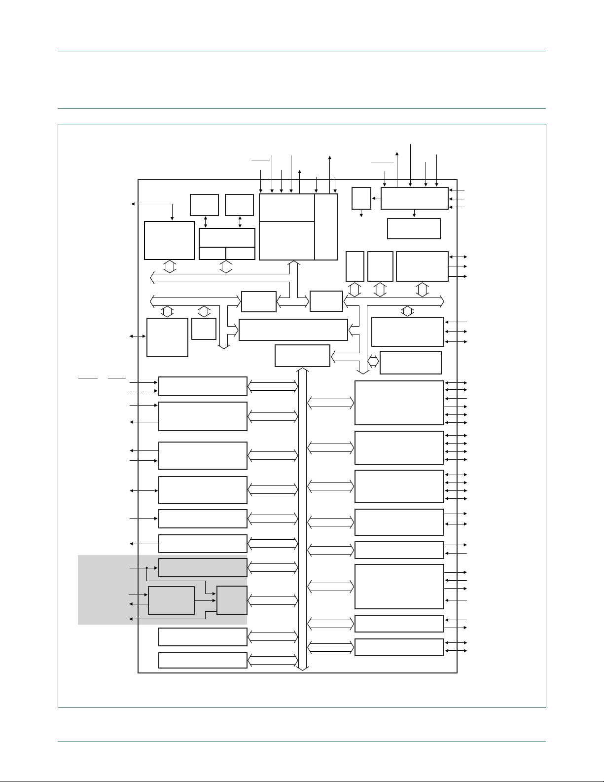
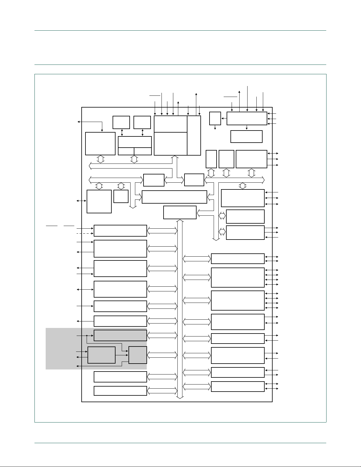
9. LPC2458 block diagram
UM10237
Chapter 1: LPC24XX Introductory information
Fig 1. LPC2458 block diagram
UM10237_2 © NXP B.V. 2008. All rights reserved.
User manual Rev. 02 — 19 December 2008 11 of 792
Page 12
NXP Semiconductors
power domain 2
LPC2420/2460
A[23:0]
D[31:0]
EXTERNAL
MEMORY
CONTROLLER
ALARM
002aad313
PWM0, PWM1
ARM7TDMI-S
PLL
EINT3 to EINT0
P3, P4
P0, P1, P2,
LEGACY GPI/O
64 PINS TOTAL
P0, P1
SCK, SCK0
MOSI, MOSI0
SSEL, SSEL0
SCK1
MOSI1
MISO1
SSEL1
SCL0, SCL1, SCL2
I2SRX_CLK
I2STX_CLK
I2SRX_WS
I2STX_WS
8 × AD0
RTCX1
RTCX2
MCICLK, MCIPWR
RXD0, RXD2, RXD3
TXD1
RXD1
RD1, RD2
TD1, TD2
CAN1
(1)
, CAN2
(1)
port1
XTAL1
TCK TDO
EXTIN0
XTAL2
RESET
TRST
TDITMS
HIGH-SPEED
GPI/O
160 PINS
TOTAL
port2
64 kB
SRAM
INTERNAL
SRAM
CONTROLLER
TEST/DEBUG
INTERFACE
EMULATION
TRACE MODULE
trace signals
AHB
BRIDGE
AHB
BRIDGE
ETHERNET
MAC WITH
DMA
(1)
16 kB
SRAM
(1)
MASTER
PORT
AHB TO
AHB BRIDGE
SLAVE
PORT
system
clock
SYSTEM
FUNCTIONS
INTERNAL RC
OSCILLATOR
V
DDA
V
DD(3V3)
V
DD(DCDC)(3V3)
VREF
V
SSA
, V
SSCORE
, V
SSIO
VIC
16 kB
SRAM
USB DEVICE/
HOST/OTG WITH
4 kB RAM AND DMA
GP DMA
CONTROLLER
I2S INTERFACE
SPI, SSP0 INTERFACE
I2SRX_SDA
I2STX_SDA
MISO, MISO0
SSP1 INTERFACE
SD/MMC CARD
INTERFACE
MCICMD,
MCIDAT[3:0]
TXD0, TXD2, TXD3
UART0, UART2, UART3
UART1
DTR1, RTS1
DSR1, CTS1, DCD1,
RI1
I
2
C0, I2C1, I2C2
SDA0, SDA1, SDA2
EXTERNAL INTERRUPTS
CAPTURE/COMPARE
TIMER0/TIMER1/
TIMER2/TIMER3
A/D CONVERTER
D/A CONVERTER
2 kB BATTERY RAM
RTC
OSCILLATOR
REAL-
TIME
CLOCK
WATCHDOG TIMER
SYSTEM CONTROL
2 × CAP0/CAP1/
CAP2/CAP3
4 × MAT2/MAT3,
2 × MAT0,
3 × MAT1
6 × PWM0/PWM1
1 × PCAP0,
2 × PCAP1
AOUT
VBAT
AHB TO
APB BRIDGE
MII/RMII
V
BUS
DBGEN
P0, P2
AHB2
AHB1
control lines
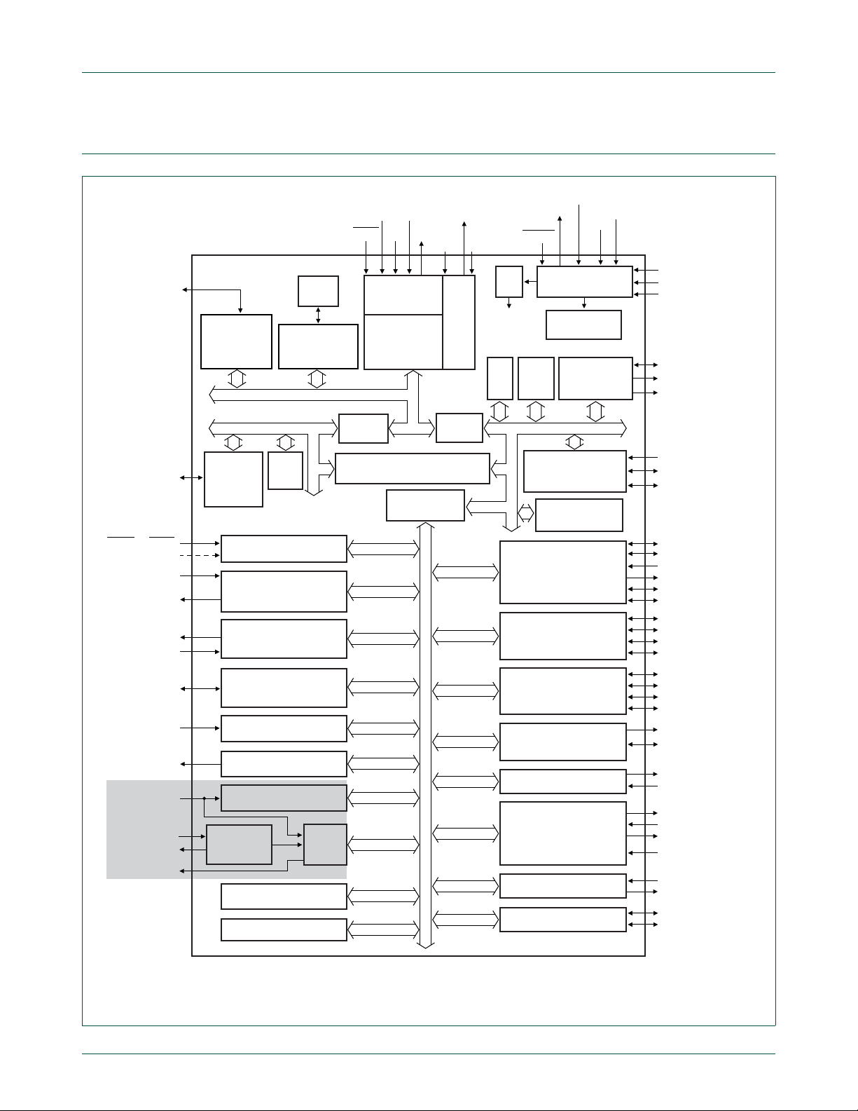
10. LPC2420/60 block diagram
UM10237
Chapter 1: LPC24XX Introductory information
(1) LPC2460 only.
Fig 2. LPC2460 block diagram
UM10237_2 © NXP B.V. 2008. All rights reserved.
User manual Rev. 02 — 19 December 2008 12 of 792
Page 13
NXP Semiconductors
power domain 2
LPC2468
A[23:0]
D[31:0]
EXTERNAL
MEMORY
CONTROLLER
ALARM
002aac721
PWM0, PWM1
ARM7TDMI-S
PLL
EINT3 to EINT0
FLASH
P3, P4
P0, P1, P2,
LEGACY GPI/O
64 PINS TOTAL
P0, P1
SCK, SCK0
MOSI, MOSI0
SSEL, SSEL0
SCK1
MOSI1
MISO1
SSEL1
SCL0, SCL1, SCL2
I2SRX_CLK
I2STX_CLK
I2SRX_WS
I2STX_WS
8 × AD0
RTCX1
RTCX2
MCICLK, MCIPWR
RXD0, RXD2, RXD3
TXD1
RXD1
RD1, RD2
TD1, TD2
CAN1, CAN2
port1
XTAL1
TCK TDO
EXTIN0
XTAL2
RESET
TRST
TDITMS
HIGH-SPEED
GPI/O
160 PINS
TOTAL
port2
64 kB
SRAM
512 kB
FLASH
INTERNAL
CONTROLLERS
TEST/DEBUG
INTERFACE
EMULATION
TRACE MODULE
trace signals
AHB
BRIDGE
AHB
BRIDGE
ETHERNET
MAC WITH
DMA
16 kB
SRAM
MASTER
PORT
AHB TO
AHB BRIDGE
SLAVE
PORT
system
clock
SYSTEM
FUNCTIONS
INTERNAL RC
OSCILLATOR
V
DDA
V
DD(3V3)
V
DD(DCDC)(3V3)
VREF
V
SSA
, V
SSIO, VSSCORE
VIC
16 kB
SRAM
USB DEVICE/
HOST/OTG WITH
4 kB RAM AND DMA
GP DMA
CONTROLLER
I2S INTERFACE
SPI, SSP0 INTERFACE
I2SRX_SDA
I2STX_SDA
MISO, MISO0
SSP1 INTERFACE
SD/MMC CARD
INTERFACE
MCICMD,
MCIDAT[3:0]
TXD0, TXD2, TXD3
UART0, UART2, UART3
UART1
DTR1, RTS1
DSR1, CTS1, DCD1,
RI1
I
2
C0, I2C1, I2C2
SDA0, SDA1, SDA2
EXTERNAL INTERRUPTS
CAPTURE/COMPARE
TIMER0/TIMER1/
TIMER2/TIMER3
A/D CONVERTER
D/A CONVERTER
2 kB BATTERY RAM
RTC
OSCILLATOR
REAL-
TIME
CLOCK
WATCHDOG TIMER
SYSTEM CONTROL
2 × CAP0/CAP1/
CAP2/CAP3
4 × MAT2/MAT3,
2 × MAT0,
3 × MAT1
6 × PWM0/PWM1
1 × PCAP0,
2 × PCAP1
AOUT
VBAT
AHB TO
APB BRIDGE
SRAM
MII/RMII
V
BUS
DBGEN
P0, P2
AHB2
AHB1
control lines
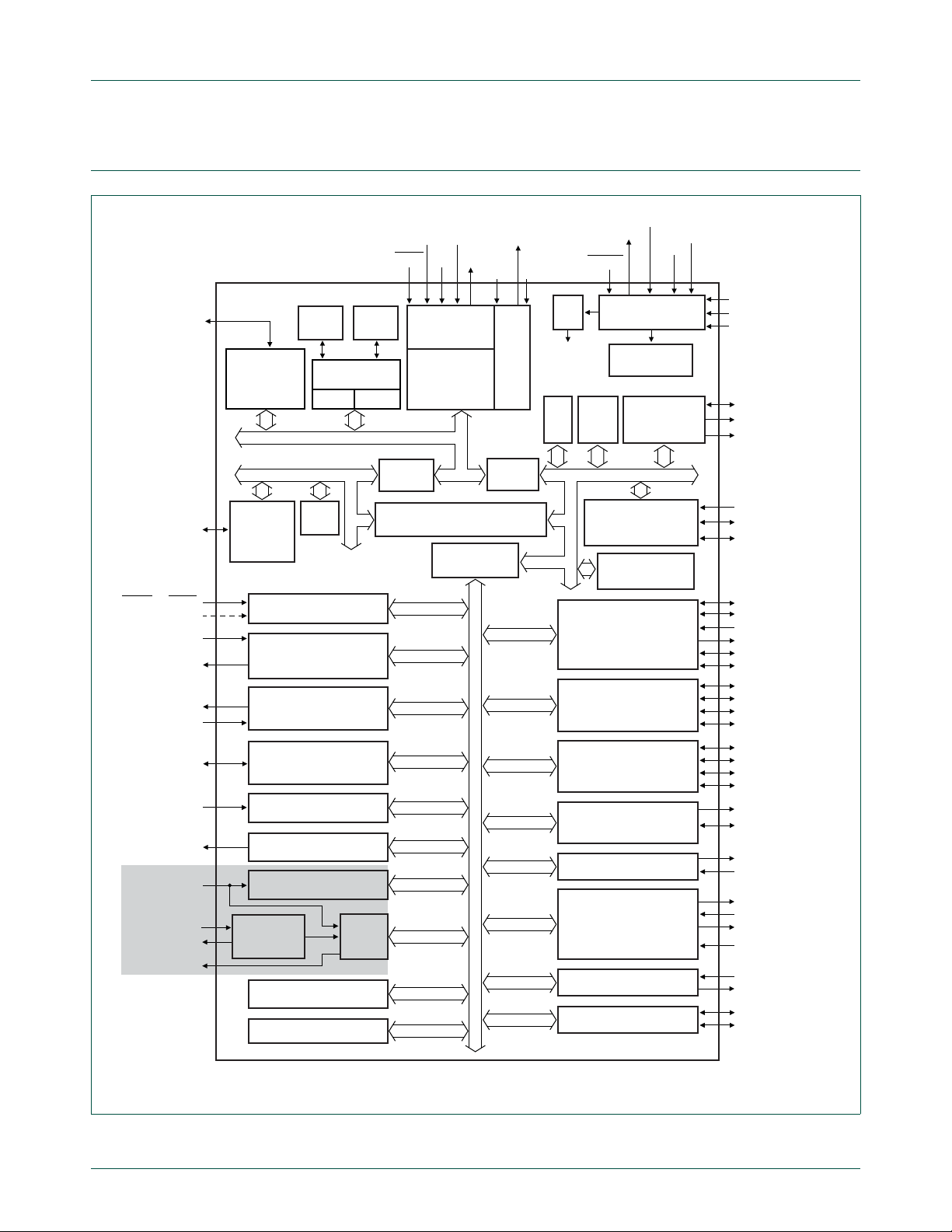
11. LPC2468 block diagram
UM10237
Chapter 1: LPC24XX Introductory information
Fig 3. LPC2468 block diagram
UM10237_2 © NXP B.V. 2008. All rights reserved.
User manual Rev. 02 — 19 December 2008 13 of 792
Page 14
NXP Semiconductors
power domain 2
LPC2470
A[23:0]
D[31:0]
EXTERNAL
MEMORY
CONTROLLER
ALARM
002aad317
PWM0, PWM1
ARM7TDMI-S
PLL
EINT3 to EINT0
P3, P4
P0, P1, P2,
LEGACY GPI/O
64 PINS TOTAL
P0, P1
SCK, SCK0
3 × I2STX
3 × I2SRX
8 × LCD control
LCDVD[23:0]
LCDCLKIN
MOSI, MOSI0
SSEL, SSEL0
SCK1
MOSI1
MISO1
SSEL1
SCL0, SCL1, SCL2
8 × AD0
RTCX1
RTCX2
MCICLK, MCIPWR
RXD0, RXD2, RXD3
RD1, RD2
TD1, TD2
CAN1, CAN2
port1
XTAL1
TCK TDO
EXTIN0
XTAL2
RESET
TRST
TDITMS
HIGH-SPEED
GPI/O
160 PINS
TOTAL
port2
64 kB
SRAM
INTERNAL
SRAM
CONTROLLER
TEST/DEBUG
INTERFACE
EMULATION
TRACE MODULE
trace signals
AHB
BRIDGE
AHB
BRIDGE
ETHERNET
MAC WITH
DMA
16 kB
SRAM
MASTER
PORT
AHB TO
AHB BRIDGE
SLAVE
PORT
system
clock
SYSTEM
FUNCTIONS
INTERNAL RC
OSCILLATOR
V
DDA
V
DD(3V3)
V
DD(DCDC)(3V3)
VREF
VIC
16 kB
SRAM
USB DEVICE/
HOST/OTG WITH
4 kB RAM AND DMA
GP DMA
CONTROLLER
LCD INTERFACE
WITH DMA
I2S INTERFACE
SPI, SSP0 INTERFACE
MISO, MISO0
SSP1 INTERFACE
SD/MMC CARD
INTERFACE
MCICMD,
MCIDAT[3:0]
TXD0, TXD2, TXD3
UART0, UART2, UART3
UART1
TXD1, DTR1, RTS1
RXD1, DSR1, CTS1,
DCD1, RI1
I
2
C0, I2C1, I2C2
SDA0, SDA1, SDA2
EXTERNAL INTERRUPTS
CAPTURE/COMPARE
TIMER0/TIMER1/
TIMER2/TIMER3
A/D CONVERTER
D/A CONVERTER
2 kB BATTERY RAM
RTC
OSCILLATOR
REAL-
TIME
CLOCK
WATCHDOG TIMER
SYSTEM CONTROL
2 × CAP0/CAP1/
CAP2/CAP3
4 × MAT2/MAT3,
2 × MAT0,
3 × MAT1
6 × PWM0/PWM1
1 × PCAP0,
2 × PCAP1
AOUT
VBAT
AHB TO
APB BRIDGE
MII/RMII
V
BUS
DBGEN
P0, P2
AHB2
AHB1
control lines
V
SSA
, V
SSCORE
, V
SSIO
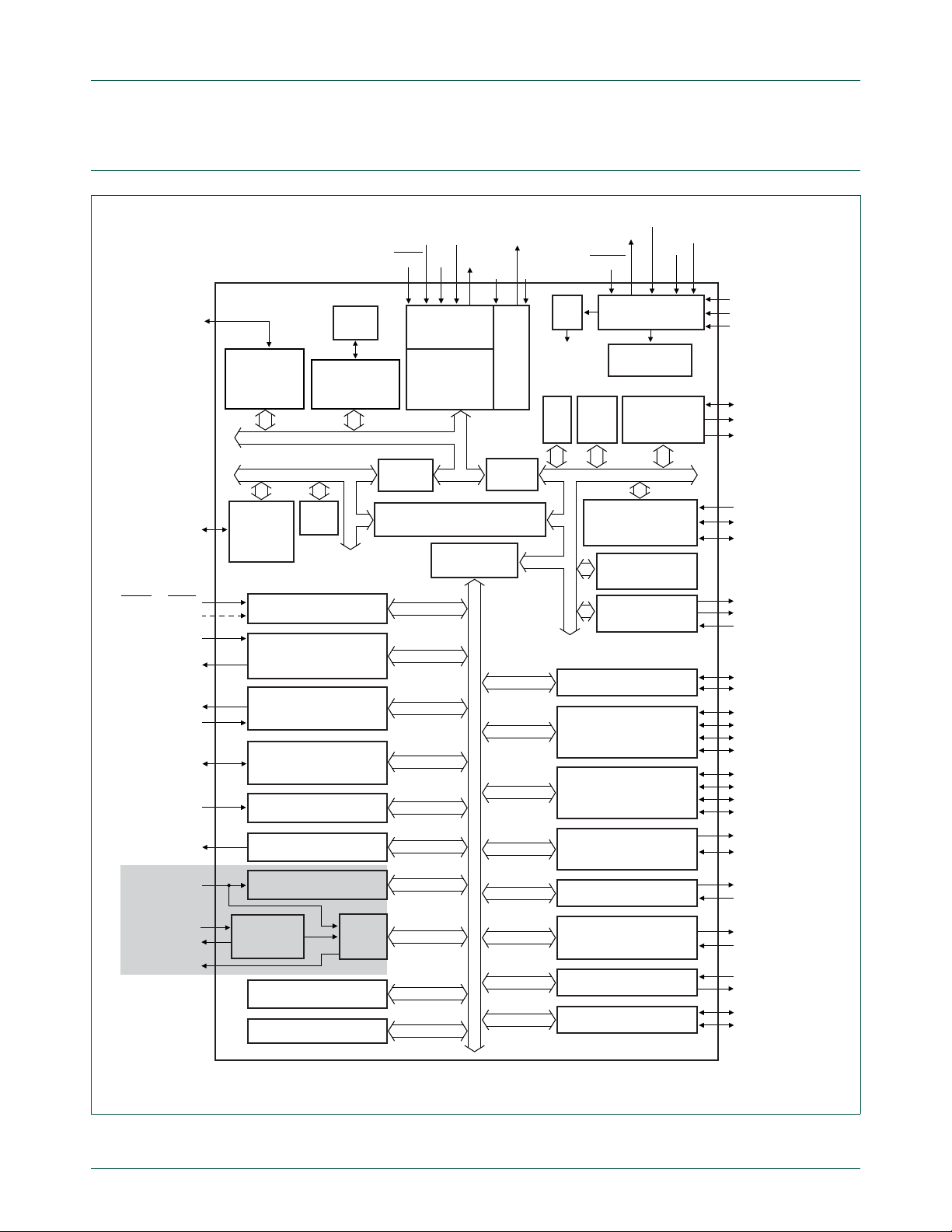
12. LPC2470 block diagram
UM10237
Chapter 1: LPC24XX Introductory information
Fig 4. LPC2470 block diagram
UM10237_2 © NXP B.V. 2008. All rights reserved.
User manual Rev. 02 — 19 December 2008 14 of 792
Page 15
NXP Semiconductors
power domain 2
LPC2478
A[23:0]
D[31:0]
EXTERNAL
MEMORY
CONTROLLER
ALARM
002aac805
PWM0, PWM1
ARM7TDMI-S
PLL
EINT3 to EINT0
FLASH
P3, P4
P0, P1, P2,
LEGACY GPI/O
64 PINS TOTAL
P0, P1
SCK0, SCK
3 × I2STX
3 × I2SRX
8 × LCD control
LCDVD[23:0]
LCDCLKIN
MOSI0, MOSI
SSEL0, SSEL
SCK1
MOSI1
MISO1
SSEL1
SCL0, SCL1, SCL2
8 × AD0
RTCX1
RTCX2
MCICLK, MCIPWR
RXD0, RXD2, RXD3
RD1, RD2
TD1, TD2
CAN1, CAN2
port1
XTAL1
TCK TDO
EXTIN0
XTAL2
RESET
TRST
TDITMS
HIGH-SPEED
GPI/O
160 PINS
TOTAL
port2
64 kB
SRAM
512 kB
FLASH
INTERNAL
CONTROLLERS
TEST/DEBUG
INTERFACE
EMULATION
TRACE MODULE
trace signals
AHB
BRIDGE
AHB
BRIDGE
ETHERNET
MAC WITH
DMA
16 kB
SRAM
MASTER
PORT
AHB TO
AHB BRIDGE
SLAVE
PORT
system
clock
SYSTEM
FUNCTIONS
INTERNAL RC
OSCILLATOR
V
DDA
V
DD(3V3)
V
DD(DCDC)(3V3)
VREF
V
SSA
, V
SSIO, VSSCORE
VIC
16 kB
SRAM
USB DEVICE/
HOST/OTG WITH
4 kB RAM AND DMA
GP DMA
CONTROLLER
LCD INTERFACE
WITH DMA
I2S INTERFACE
SSP0/SPI INTERFACE
MISO0, MISO
SSP1 INTERFACE
SD/MMC CARD
INTERFACE
MCICMD,
MCIDAT[3:0]
TXD0, TXD2, TXD3
UART0, UART2, UART3
UART1
TXD1, DTR1, RTS1
RXD1, DSR1, CTS1,
DCD1, RI1
I
2
C0, I2C1, I2C2
SDA0, SDA1, SDA2
EXTERNAL INTERRUPTS
CAPTURE/COMPARE
TIMER0/TIMER1/
TIMER2/TIMER3
A/D CONVERTER
D/A CONVERTER
2 kB BATTERY RAM
RTC
OSCILLATOR
REAL-
TIME
CLOCK
WATCHDOG TIMER
SYSTEM CONTROL
2 × CAP0/CAP1/
CAP2/CAP3
4 × MAT2/MAT3,
2 × MAT0,
3 × MAT1
6 × PWM0/PWM1
1 × PCAP0,
2 × PCAP1
AOUT
VBAT
AHB TO
APB BRIDGE
SRAM
MII/RMII
V
BUS
DBGEN
P0, P2
AHB2
AHB1
control lines
13. LPC2478 block diagram
UM10237
Chapter 1: LPC24XX Introductory information
Fig 5. LPC2478 block diagram
UM10237_2 © NXP B.V. 2008. All rights reserved.
User manual Rev. 02 — 19 December 2008 15 of 792
Page 16

UM10237
Chapter 2: LPC24XX Memory mapping
Rev. 02 — 19 December 2008 User manual
1. How to read this chapter
The memory addressing and mapping for dif fere nt LPC2400 parts depends on flash size,
EMC size, and the LCD peripheral, see Table 2–13
T able 13. LPC2400 memory options and addressing
LPC2458 512 kB no 16-bit Table 2–14
LPC2420 flashless no 32-bit Table 2–15
LPC2460 flashless no 32-bit Table 2–15
LPC2468 512 kB no 32-bit Table 2–16
LPC2470 flashless yes 32-bit Table 2–15
LPC2478 512 kB yes 32-bit Table 2–16
.
Flash LCD EMC Memory map
T able 2–19;
T able 2–21
Figure 2–8
2. Memory map and peripheral addressing
ARM processors have a single 4 GB address space. The following table shows how this
space is used on NXP embedded ARM devices.
Table 14. LPC2458 memory usage and details
Address range General use Address range details and description
0x0000 0000 to
0x3FFF FFFF
0x4000 0000 to
0x7FFF FFFF
0x8000 0000 to
0xDFFF FFFF
0xE000 0000 to
0xEFFF FFFF
0xF000 0000 to
0xFFFF FFFF
On-chip non-volatile
memory and Fast I/O
On-chip RAM 0x4000 0000 - 0x4000 FFFF RAM (64 k B)
Off-Chip Memory Two static memory banks, 16 MB each
APB Peripherals 36 peripheral blocks, 16 kB each
AHB peripherals
0x0000 0000 - 0x0007 FFFF Flash Memory (512 kB)
0x3FFF C 000 - 0x3FFF FFFF Fast GPIO registers
0x7FE0 0000 - 0x7FE0 3FFF Ethernet RAM (16 kB)
0x7FD0 000 0 - 0x7FD0 3FFF USB RAM (16kB)
0x8000 0000 - 0x80FF FFFF Static memory bank 0
0x8100 0000 - 0x81FF FFFF Static memory bank 1
Two dynamic memory banks, 256 MB each
0xA000 0000 - 0xAFFF FFFF Dynamic memory bank 0
0xB000 0000 - 0xBFFF FFFF Dynamic memory bank 1
UM10237_2 © NXP B.V. 2008. All rights reserved.
User manual Rev. 02 — 19 December 2008 16 of 792
Page 17

NXP Semiconductors
UM10237
Chapter 2: LPC24XX Memory mapping
Table 15. LPC2420/60/70 memory usage and details
Address range General use Address range details and description
0x0000 0000 to
0x3FFF FFFF
0x4000 0000 to
0x7FFF FFFF
Fast I/O 0x0000 0000 - 0x0007 FFFF Reserved (flashless parts)
0x3FFF C 000 - 0x3FFF FFFF Fast GPIO registers
On-chip RAM 0x4000 0000 - 0x4000 FFFF RAM (64 k B)
0x7FE0 0000 - 0x7FE0 3FFF Ethernet RAM (16 kB) (LPC2460
0x7FD0 000 0 - 0x7FD0 3FFF USB RAM (16kB)
0x8000 0000 to
0xDFFF FFFF
Off-Chip Memory Four static memory banks, 16 MB each
0x8000 0000 - 0x80FF FFFF Static memory bank 0
0x8100 0000 - 0x81FF FFFF Static memory bank 1
0x8200 0000 - 0x82FF FFFF Static memory bank 2
0x8300 0000 - 0x83FF FFFF Static memory bank 3
Four dynamic memory banks, 256 MB each
0xA000 0000 - 0xAFFF FFFF Dynamic memory bank 0
0xB000 0000 - 0xBFFF FFFF Dynamic memory bank 1
0xC000 0000 - 0xCFFF FFFF Dynamic memory bank 2
0xD000 0000 - 0xDFFF FFFF Dynamic memory bank 3
0xE000 0000 to
APB Peripherals 36 peripheral blocks, 16 kB each
0xEFFF FFFF
0xF000 0000 to
AHB peripherals
0xFFFF FFFF
only)
Table 16. LPC2468/78 memory usage and details
Address range General use Address range details and description
0x0000 0000 to
0x3FFF FFFF
0x4000 0000 to
0x7FFF FFFF
On-chip non-volatile
memory and Fast I/O
0x0000 0000 - 0x0007 FFFF Flash Memory (512 kB)
0x3FFF C 000 - 0x3FFF FFFF Fast GPIO registers
On-chip RAM 0x4000 0000 - 0x4000 FFFF RAM (64 k B)
0x7FE0 0000 - 0x7FE0 3FFF Ethernet RAM (16 kB)
0x7FD0 000 0 - 0x7FD0 3FFF USB RAM (16kB)
UM10237_2 © NXP B.V. 2008. All rights reserved.
User manual Rev. 02 — 19 December 2008 17 of 792
Page 18

NXP Semiconductors
Chapter 2: LPC24XX Memory mapping
Table 16. LPC2468/78 memory usage and details
Address range General use Address range details and description
0x8000 0000 to
0xDFFF FFFF
0xE000 0000 to
0xEFFF FFFF
0xF000 0000 to
0xFFFF FFFF
Off-Chip Memory Four static memory banks, 16 MB each
0x8000 0000 - 0x80FF FFFF Static memory bank 0
0x8100 0000 - 0x81FF FFFF Static memory bank 1
0x8200 0000 - 0x82FF FFFF Static memory bank 2
0x8300 0000 - 0x83FF FFFF Static memory bank 3
Four dynamic memory banks, 256 MB each
0xA000 0000 - 0xAFFF FFFF Dynamic memory bank 0
0xB000 0000 - 0xBFFF FFFF Dynamic memory bank 1
0xC000 0000 - 0xCFFF FFFF Dynamic memory bank 2
0xD000 0000 - 0xDFFF FFFF Dynamic memory bank 3
APB Peripherals 36 peripheral blocks, 16 kB each
AHB peripherals
UM10237
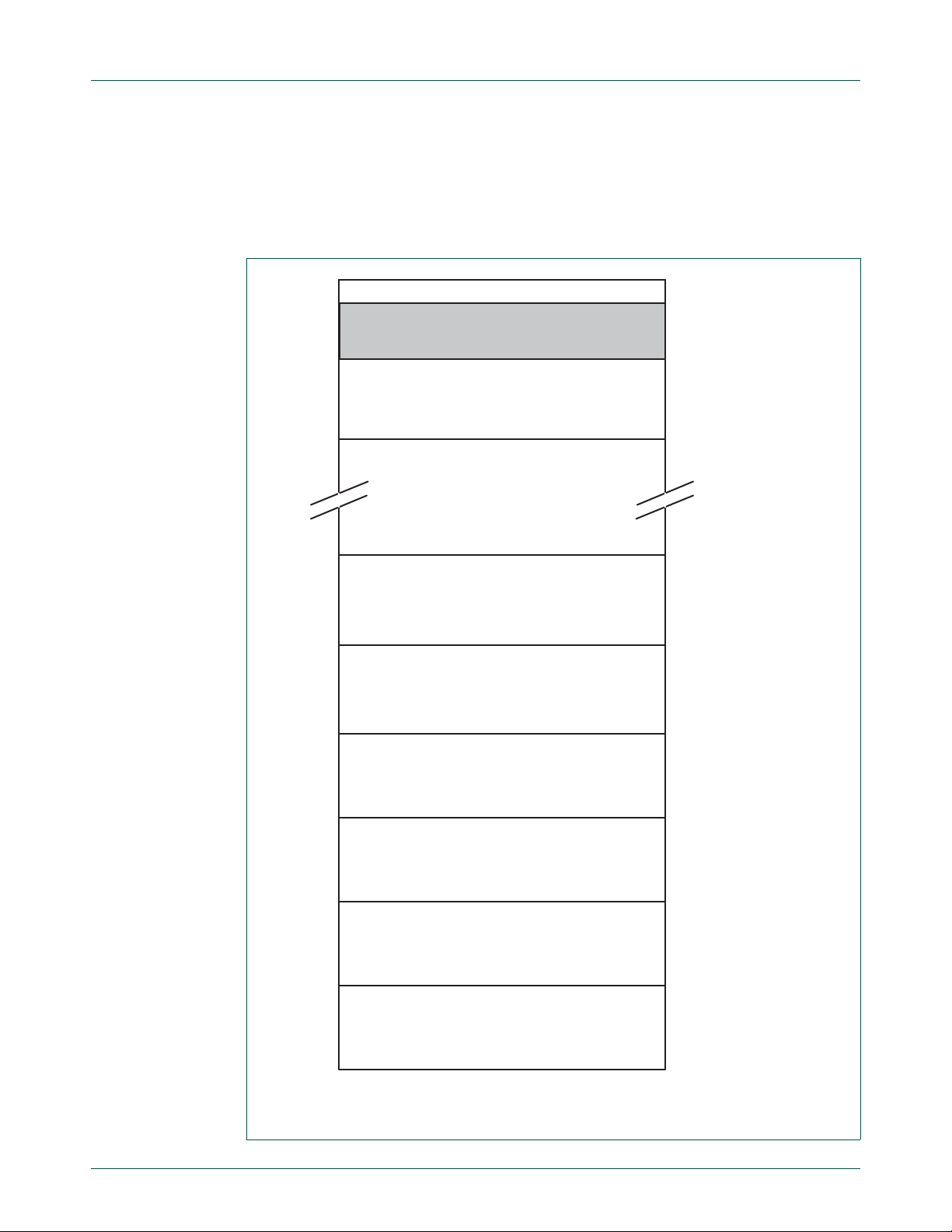
3. Memory maps
The LPC2400 incorporates several distinct memory regions, shown in the following
figures. Figure 2–6
program viewpoint following reset. The interrupt vector area supports address remapping,
which is described later in this section.
shows the overall map of the entire address space from the user
UM10237_2 © NXP B.V. 2008. All rights reserved.
User manual Rev. 02 — 19 December 2008 18 of 792
Page 19

NXP Semiconductors
0.0 GB
1.0 GB
ON-CHIP NON-VOLATILE MEMORY OR RESERVED
0x0000 0000
RESERVED ADDRESS SPACE
SPECIAL REGISTERS
ON-CHIP STATIC RAM
RESERVED ADDRESS SPACE
0x4000 0000
0x3FFF 8000
0x3FFF FFFF
2.0 GB 0x8000 0000
0x7FFF FFFF
BOOT ROM AND BOOT FLASH
EXTERNAL STATIC AND DYNAMIC MEMORY
3.75 GB
4.0 GB
3.5 GB
AHB PERIPHERALS
APB PERIPHERALS
0xE000 0000
0xF000 0000
0xFFFF FFFF
UM10237
Chapter 2: LPC24XX Memory mapping
Fig 6. LPC2400 system memory map
UM10237_2 © NXP B.V. 2008. All rights reserved.
User manual Rev. 02 — 19 December 2008 19 of 792
Page 20

NXP Semiconductors
RESERVED
RESERVED
0xF000 0000
0xEFFF FFFF
APB PERIPHERALS
0xE020 0000
0xE01F FFFF
0xE000 0000
AHB PERIPHERALS
0xFFFF FFFF
0xFFE0 0000
0xFFDF FFFF
3.75 GB
3.5 GB
3.5 GB + 2 MB
4.0 GB - 2 MB
4.0 GB
UM10237
Chapter 2: LPC24XX Memory mapping
Fig 7. Peripheral memory map
Figure 8 and Table 2–17 show different views of the peripheral address space. Both the
AHB and APB peripheral areas are 2 megabyte spaces which are divided up into 128
peripherals. Each peripheral space is 16 kilobytes in size. This allows simplifying the
address decoding for each peripheral.
UM10237_2 © NXP B.V. 2008. All rights reserved.
User manual Rev. 02 — 19 December 2008 20 of 792
Page 21
NXP Semiconductors
VECTORED INTERRUPT CONTROLLER
(AHB PERIPHERAL #0)
0xFFFF F000 (4G - 4K)
0xFFFF C000
0xFFFF 8000
(AHB PERIPHERAL #4)
(AHB PERIPHERAL #3)
(AHB PERIPHERAL #2)
(AHB PERIPHERAL #1)
(AHB PERIPHERAL #126)
0xFFE1 8000
0xFFE1 4000
0xFFE1 0000
0xFFE0 C000
0xFFE0 8000
0xFFE0 4000
0xFFE0 0000
ETHERNET CONTROLLER
GENERAL PURPOSE DMA CONTROLLER
EXTERNAL MEMORY CONTROLLER
USB CONTROLLER
LCD
(1)
(AHB PERIPHERAL #5)
NOT USED
All peripheral register addresses are word aligned (to 32 bit boundaries) regardless of
their size. This eliminates the need for byte lane mapping hardware that would be required
to allow byte (8 bit) or half-word (16 bit) accesses to occur at smaller boundaries. An
implication of this is that word and half-word registers must be accessed all at once. For
example, it is not possible to read or write the upper byte of a word register separately.
UM10237
Chapter 2: LPC24XX Memory mapping
UM10237_2 © NXP B.V. 2008. All rights reserved.
User manual Rev. 02 — 19 December 2008 21 of 792
(1) LPC247x only.
Fig 8. AHB periphera l map
Page 22

NXP Semiconductors
4. APB peripheral addresses
The following table shows the APB address map. No APB peripheral uses all of the 16 kB
space allocated to it. T ypically each device’ s registers are "aliased" or re peated at multiple
locations within each 16 kB range.
Table 17. APB peripherals and base addresses
APB Peripheral Base Address Peripheral Name
0 0xE000 0000 Watchdog Timer
1 0xE000 400 0 Timer 0
2 0xE000 800 0 Timer 1
3 0xE000 C000 UART0
4 0xE001 0000 UART1
5 0xE001 4000 PWM0
6 0xE001 8000 PWM1
7 0xE001 C000 I
8 0xE002 0000 SPI
9 0xE002 4000 RTC
10 0xE002 8000 GPIO
1 1 0xE002 C000 Pin Connect Block
12 0xE003 0000 SSP1
13 0xE003 4000 ADC
14 0xE003 800 0 CAN Acceptance Filter RAM
15 0xE003 C000 CAN Acceptance Filter Registers
16 0xE004 000 0 CAN Common Registers
17 0xE004 400 0 CAN Con trol ler 1
18 0xE004 800 0 CAN Con trol ler 2
19 to 22 0xE004 C000 to 0xE005 8000 Not used
23 0xE005 C000 I
24 0xE006 0000 Not used
25 0xE006 4000 Not used
26 0xE006 8000 SSP0
27 0xE006 C000 DAC
28 0xE007 000 0 Timer 2
29 0xE007 400 0 Timer 3
30 0xE007 8000 UART2
31 0xE007 C000 UART3
32 0xE008 0000 I
33 0xE008 4000 Battery RAM
34 0xE008 8000 I2S
35 0xE008 C000 SD/MMC Card Interface
36 to 126 0xE009 0000 to 0xE01F BFFF Not used
127 0xE01F C000 System Control Block
UM10237
Chapter 2: LPC24XX Memory mapping
2
C0
2
C1
2
C2
UM10237_2 © NXP B.V. 2008. All rights reserved.
User manual Rev. 02 — 19 December 2008 22 of 792
Page 23

NXP Semiconductors
Chapter 2: LPC24XX Memory mapping
5. LPC2400 memory re-mapping and boot ROM
5.1 Memory map concepts and operating modes
The basic concept on the LPC2400 is that each memory area has a "natural" location in
the memory map. This is the address range for which code residing in that area is written.
The bulk of each memory space remains permanently fixed in the same location,
eliminating the need to have portions of the code designed to run in different address
ranges.
Because of the location of the interrupt vectors on the ARM7 processor (at addresses
0x0000 0000 through 0x0000 001C, as shown in Table 2–18
Boot ROM and SRAM spaces need to be re-mapped in order to allow alternative uses of
interrupts in the differen t operating modes described in Table 2–19
interrupts is accomplished via the Memory Mapping Contro l feature (Section 2–6 “
mapping control” on page 25).
Table 18. ARM exception vector locations
Address Exception
0x0000 0000 Reset
0x0000 0004 Undefined Instruction
0x0000 0008 Software Interrupt
0x0000 000C Prefetch Abort (instruction fetch memory fault)
0x0000 0010 Data Abort (data access memory fault)
0x0000 0014 Reserved
Note: Identified as reserved in ARM documentation, this location is used
by the Boot Loader as the Valid User Program key when booting from
on-chip flash memory. This is described in detail in Section 30–5.1.1
0x0000 0018 IRQ
0x0000 001C FIQ
UM10237
below), a small portion of the
. Re-mapping of the
Memory
.
UM10237_2 © NXP B.V. 2008. All rights reserved.
User manual Rev. 02 — 19 December 2008 23 of 792
Page 24

NXP Semiconductors
Table 19. LPC2400 Memory mapping modes
Mode Activation Usage
Boot
Loader
mode
User
Flash
mode
User RAM
mode
User
External
memory
mode
Hardware
activation by
any Reset
Software
activation by
Boot code
Software
activation by
User program
Software
activation by
user code
Software
activation by
boot code
UM10237
Chapter 2: LPC24XX Memory mapping
The Boot Loader always executes after any reset. The Boot ROM
interrupt vectors are mapped to the bottom of memory to allow
handling exceptions and using interrupts during the Boot Loading
process. A sector of the flash memory (the Boot flash) is available to
hold part of the Boot Code.
For LPC2400 parts with flash only . Activated by the Boot Loader when
a valid User Program Signature is recognized in memory and Boot
Loader operation is not forced. Interrupt vectors are not re-mapped
and are found in the bottom of the flash memory.
Activated by a User Program as desired. Interrupt vectors are
re-mapped to the bottom of the Static RAM.
For LPC2400 parts with flash. Interrupt vectors are re-mapped to
external memory bank 0.
For flashless parts LPC2420/60/70 only. Interrupt vectors are
re-mapped to external memory bank 0.
[1]
[2]
[1] See EMCControl register address mirror bit in Table 5–68 for address of external memory bank 0.
[2] Connect external boot memory to chip select 1. During boot from external memory, the address mirror bit is
set and memory bank addresses 0 and 1 are swapped.
5.2 Memory re-mapping
In order to allow for compatibility with future derivatives, the entire Boot ROM is mapped
to the top of the on-chip memory space. In this manner, the use of larger or smaller flash
modules will not require changing the location of the Boot ROM (which would require
changing the Boot Loader code itself) or changing the mapping of the Boot ROM interru pt
vectors. Memory spaces other than the interrupt vectors remain in fixed locations.
Figure 2–9
The portion of memory that is re-mapped to allow interrupt processing in different modes
includes the interrupt vector area (32 bytes) and an additional 32 bytes for a total of
64 bytes, that facilitates branching to interrupt handlers at distant physical addresses. The
remapped code locations overlay addresses 0x0000 0000 through 0x0000 003F. A typical
user program in the flash memory can place the entire FIQ handler at address
0x0000 001C without any nee d to cons ide r me mory boundaries. The vector contained in
the SRAM, external memory , and Boot ROM must cont ain branches to the actual interrupt
handlers, or to other instructions that accomplish the branch to the interrupt hand lers.
There are three reasons this configuration was chosen:
1. To give the FIQ handler in the flash memory the advantage of not having to take a
2. Minimize the need to for the SRAM and Boot ROM vectors to deal with arbitrary
3. To provide space to store constants for jumping beyond the range of single word
shows the on-chip memory mapping in the modes defined above.
memory boundary caused by the remapping into account.
boundaries in the middle of code space.
branch instructions.
UM10237_2 © NXP B.V. 2008. All rights reserved.
User manual Rev. 02 — 19 December 2008 24 of 792
Page 25

NXP Semiconductors
Re-mapped memory areas, including the Boot ROM and interrupt vectors, continue to
appear in their original location in addition to the re-mapped address.
UM10237
Chapter 2: LPC24XX Memory mapping
Details on re-mapping and examples can be found in Section 2–6 “
control” on page 25.
6. Memory mapping control
The Memory Mapping Control alters the mapping of the interrupt vectors that appear
beginning at address 0x0000 0000. This allows code running in different memory spaces
to have control of the interrupts.
6.1 Memory Mapping Control Register (MEMMAP - 0xE01F C040)
Whenever an exception handling is necessary , the microcontroller will fetch an instruction
residing on exception corresponding address as described in Table 2–18 “
vector locations” on page 23. The MEMMAP register determines the source of data that
will fill this table.
Table 20. Memory mapping control registers
Name Description Access Reset
MEMMAP Memory mapping control. Selects whether the
ARM interrupt vectors are read from the Boot
ROM, User Flash, or RAM.
Table 21. Memory Mapping control register (MEMMAP - address 0xE01F C040) bit
description
Bit Symbol Value Description Reset
1:0 MAP 00 Boot Loader Mode. Interrupt vectors are re-mapped to Boot ROM. 00
01 User Flash Mode. Interrupt vectors are not re-mapped and reside
10 User RAM Mode. Interrupt vect ors are re-mapped to Static RAM.
11 User External Memory Mode. Interrupt vectors are re-mapped to
Warning: Improper setting of this value may result in incorrect operation of
the device.
7:2 - - Reserved, user software should not write ones to reserved bits.
Memory mapping
ARM exception
Address
value
R/W 0x00 0xE01F C040
value
in Flash.
Remark: This mode is for parts with flash only. Value 01 is
reserved for flashless parts LPC2420/60/70.
external memory bank 0.
NA
The value read from a reserved bit is not defined.
6.2 Memory mapping control usage notes
Memory Mapping Control simply selects one out of three available sources of data (set s of
64 bytes each) necessary for handling ARM exceptions (interrupts).
For example, whenever a Software Interrupt request is generated, ARM core will always
fetch 32 bit data "residing" on 0x0000 0008 see Table 2–18 “
locations” on page 23. This means that when MEMMAP[1:0] = 10 (User RAM Mode),
UM10237_2 © NXP B.V. 2008. All rights reserved.
User manual Rev. 02 — 19 December 2008 25 of 792
ARM exception vector
Page 26
NXP Semiconductors
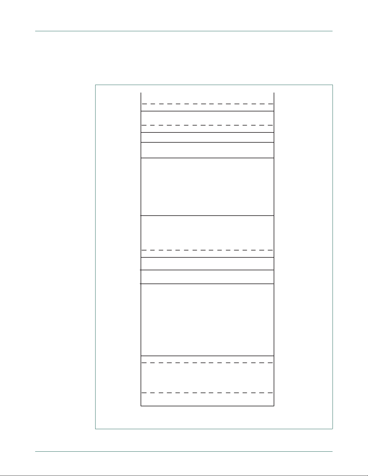
0.0 GB
0x8000 0000
0x4000 0000
0x3FFF FFFF
0x0000 0000
1.0 GB
2.0 GB - 8 kB
2.0 GB
ACTIVE INTERRUPT VECTORS
(FROM FLASH, SRAM, BOOT ROM, OR EXT MEMORY)
BOOT FLASH
RESERVED ADDRESS SPACE
(SRAM INTERRUPT VECTORS)
512 kB FLASH MEMORY
RESERVED FOR ADDRESS SPACE
(BOOT ROM INTERRUPT VECTORS)
8 kB BOOT ROM
64 kB STATIC RAM
0x7FFF FFFF
FAST GPIO REGISTERS
PARTCFG REGISTERS
0x3FFF 8000
0x3FFF C000
0x3FFF BFFF
8 kB BOOT FLASH
(RE-MAPPED FROM TOP OF FLASH MEMORY)
EXTERNAL MEMORY INTERRUPT VECTORS
0x7FFF E000
0x7FFE FFFF
0x7FFE E000
2.0 GB - 64 kB
2.0 GB - 72 kB
0x0007 FFFF
0x0008 0000
0x4001 0000
0x4000 FFFF
read/fetch from 0x0000 0008 will provide data stored in 0x4000 0008. In case of
MEMMAP[1:0] = 00 (Boot Loader Mode), read/fetch from 0x0000 0008 will provide data
available also at 0x7FFF E008 (Boot ROM remapped from on-chip Bootloader).
UM10237
Chapter 2: LPC24XX Memory mapping
Fig 9. Map of lower memory is showing re-mapped and re-mappable areas for a
UM10237_2 © NXP B.V. 2008. All rights reserved.
LPC2400 part with flash
User manual Rev. 02 — 19 December 2008 26 of 792
Page 27

NXP Semiconductors
7. Prefetch abort and data abort exceptions
The LPC2400 generates the appropriate bus cycle abort exception if an access is
attempted for an address that is in a reserved or unassigned address region. The regions
are:
• Areas of the memory map that are not implemented for a specific ARM derivative. Fo r
the LPC2400, these are:
– Address space between On-Chip Non-Volatile Memory and the Special Register
space. Labelled "Reserved for On-Chip Memory" in Figure 2–6
– Address space between On-Chip Static RAM and the Boot ROM. Labelled
"Reserved Address Space" in Figure 2–6
– External Memory
– Reserved regions of the AHB and APB spaces. See Figure 2–7
• Unassigned AHB peripheral spaces. See Figure 2–8.
• Unassigned APB peripheral spaces. See Table 2–17.
For these areas, both attempted data acce ss and in struction fetch genera te an exception.
In addition, a Prefetch Abort exception is generated for an y instruction fetch that maps to
an AHB or APB peripheral address, or to the Special Register space located just below
the SRAM at addresses 0x3FFF8000 through 0x3FFFFFFF.
UM10237
Chapter 2: LPC24XX Memory mapping
.
.
.
Within the address space of an existing APB peripheral, a data abort exception is not
generated in response to an access to an undefined address. Address decoding within
each peripheral is limited to that needed to distinguish defined registers within the
peripheral itself. For example, an access to address 0xE000 D000 (an undefined address
within the UART0 space) may result in an access to the register defined at address
0xE000 C000. Details of such address aliasing within a peripheral space are not defined
in the LPC2400 documentation and are not a supported feature.
If software executes a write directly to the flash mem ory, the MAM generates a data abort
exception. Flash programming must be accomplished by using the specified flash
programming interface provided by the Boot Code.
Note that the ARM core stores the Prefetch Abort flag along with the associated
instruction (which will be meaningless) in the pipeline and processes the abort only if an
attempt is made to execute the instruction fetched from the illegal address. This prevents
accidental aborts that could be caused by prefetches that occur when code is executed
very near a memory boundary.
UM10237_2 © NXP B.V. 2008. All rights reserved.
User manual Rev. 02 — 19 December 2008 27 of 792
Page 28

UM10237
Chapter 3: LPC24XX System control
Rev. 02 — 19 December 2008 User manual
1. Summary of system control block functions
The System Control Block includes several system features and control registers for a
number of functions that are not related to specific peripheral devices. These include:
• Reset
• Brown-Out Detection
• External Interrupt Input s
• Miscellaneous System Controls and Status
• Code Security vs. Debugging
Each type of function has its own register(s) if any are required and unneeded bit s are
defined as reserved in order to allow future expansion. Unrelated functions never share
the same register addresses
2. Pin description
Table 3–22 shows pins that are associated with system control block functions.
Table 22. Pin summary
Pin name Pin
EINT0 Input External Interrupt Input 0 - An active low/high level or
EINT1 Input External Interrupt Input 1 - See the EINT0 description above.
EINT2 Input External Interrupt Input 2 - See the EINT0 description above.
EINT3 Input External Interrupt Input 3 - See the EINT0 description above.
RESET
3. Register description
All registers, regardless of size, are on word address boundaries. Details of the registers
appear in the description of each function.
T able 23. Summary of system control registers
Name Description Access Reset value
External interrupts
EXTINT External Interrupt Flag Register R/W 0x00 0xE01F C140
EXTMODE External Interrupt Mode register R/W 0x00 0xE01F C148
EXTPOLAR External Interrupt Polarity Register R/W 0x00 0xE01F C14C
Pin description
direction
falling/rising edge general purpose interrupt input. This pin may be
used to wake up the processor from Idle or Power down modes.
Input External Reset input - A LOW on this pin resets the chip, causing
I/O ports and peripherals to take on their default states, and the
processor to begin execution at address 0x0000 0000.
[1]
Address
UM10237_2 © NXP B.V. 2008. All rights reserved.
User manual Rev. 02 — 19 December 2008 28 of 792
Page 29

NXP Semiconductors
T able 23. Summary of system control registers
Name Description Access Reset value
Reset
RSID Reset Source Identification
Syscon miscellaneous registers
SCS System Control and Status R/W 0x00 0xE01F C1A0
AHB priority scheduling registers
AHBCFG1 Configures the AHB1 arbiter R/W 0x0000 0145 0xE01F C188
AHBCFG2 Configures the AHB2 arbiter R/W 0x0000 0145 0xE01F C18C
[1] Reset Value reflects the data stored in used bits only. It does not include reserved bits content.
3.1 External interrupt inputs
The LPC2400 includes four External Interrupt Inputs as selectable pin functions. In
addition, external interrupts have the ability to wake up the CPU from Power down mode.
This is controlled by the register INTWAKE, which is described in the Clocking and Power
Control chapter under the Power Control heading
Register
UM10237
Chapter 3: LPC24XX System control
[1]
Address
R/W see text 0xE01F C180
3.1.1 Register description
The external interrupt function has four registers associated with it. The EXTINT register
contains the interrupt flags. The EXTMODE and EXTPOLAR registers specify the level
and edge sensitivity parameters.
Table 24. External Interrupt registers
Name Description Access Reset
EXTINT The External Interrupt Flag Register contains
interrupt flags for EINT0, EINT1, EINT2 and
EINT3. See Table 3–25
EXTMODE The External Interrupt Mode Registe r control s
whether each pin is edge- or level-sensitive.
See Table 3–26
EXTPOLAR The External Interrupt Polarity Register controls
which level or edge on each pin will cause an
interrupt. See Table 3–27
[1] Reset Value reflects the data stored in used bits only. It does not include reserved bits content.
.
.
.
R/W 0x00 0xE01F C140
R/W 0x00 0xE01F C148
R/W 0x00 0xE01F C14C
3.1.2 External Interrupt flag register (EXTINT - 0xE01F C140)
When a pin is selected for its external interrupt function, the level or edge on that pin
(selected by its bits in the EXTPOLAR a nd EXTMODE registers) will set its interrup t flag in
this register. This asserts the corresponding interrupt request to the VIC, which will cause
an interrupt if interrupts from the pin are enabled.
value
Address
[1]
Writing ones to bits EINT0 through EINT3 in EXTINT register clears the corresponding
bits. In level-sensitive mode the interrupt is cleared only when the pin is in its inactive
state.
UM10237_2 © NXP B.V. 2008. All rights reserved.
User manual Rev. 02 — 19 December 2008 29 of 792
Page 30

NXP Semiconductors
Once a bit from EINT0 to EINT3 is set and an appropriate code st arts to execute (hand ling
wakeup and/or external interrupt), this bit in EXTINT register must be cleared. Otherwise
event that was just triggered by activity on the EINT pin will not be recognized in future.
Important: whenever a change of external interrupt operating mode (i.e. active
level/edge) is performed (including the initialization of an external interrupt),
corresponding bit in the EXTINT register must be cleared! For details see Section
3–3.1.3 “External Interrupt Mode register (EXTMODE - 0xE01F C148)” and Section
3–3.1.4 “External Interrupt Polarity register (EXTPOLAR - 0xE01F C14C)”.
For example, if a system wakes up from power-down using low level on external interrupt
0 pin, its post-wakeup code must reset EINT0 bit in order to allow future entry into the
power-down mode. If EINT0 bit is left set to 1, subsequent attempt(s) to invoke
power-down mode will fail. The same goes for external interrupt handling.
More details on power-down mode will be discussed in the following chapters.
Table 25. External Interrupt Flag register (EXTINT - address 0xE01F C140) bit description
Bit Symbol Description Reset
0 EINT0 In level-sensitive mode, this bit is set if the EINT0 function is selected for its
1 EINT1 In level-sensitive mode, this bit is set if the EINT1 function is selected for its
2 EINT2 In level-sensitive mode, this bit is set if the EINT2 function is selected for its
3 EINT3 In level-sensitive mode, this bit is set if the EINT3 function is selected for its
7:4 - Reserved, user software should not write ones to reserved bits. The value
UM10237
Chapter 3: LPC24XX System control
pin, and the pin is in its active state. In edge-sensitive mode, this bit is set if
the EINT0 function is selected for its pin, and the selected edge occurs on
the pin.
This bit is cleared by writing a one to it, except in level sensitive mode when
the pin is in its active state.
pin, and the pin is in its active state. In edge-sensitive mode, this bit is set if
the EINT1 function is selected for its pin, and the selected edge occurs on
the pin.
This bit is cleared by writing a one to it, except in level sensitive mode when
the pin is in its active state.
pin, and the pin is in its active state. In edge-sensitive mode, this bit is set if
the EINT2 function is selected for its pin, and the selected edge occurs on
the pin.
This bit is cleared by writing a one to it, except in level sensitive mode when
the pin is in its active state.
pin, and the pin is in its active state. In edge-sensitive mode, this bit is set if
the EINT3 function is selected for its pin, and the selected edge occurs on
the pin.
This bit is cleared by writing a one to it, except in level sensitive mode when
the pin is in its active state.
read from a reserved bit is not defined.
[1]
[1]
[1]
[1]
value
0
0
0
0
NA
[1] Example: If the EINTx is selected to be low level sensitive and low level is present on corresponding pin,
this bit can not be cleared; this bit can be cleared only when signal on the pin becomes high.
UM10237_2 © NXP B.V. 2008. All rights reserved.
User manual Rev. 02 — 19 December 2008 30 of 792
Page 31

NXP Semiconductors
3.1.3 External Interrupt Mode register (EXTMODE - 0xE01F C148)
The bits in this register select whether ea ch EINT pin is le vel- or edge- sensitive. Only pins
that are selected for the EINT function (see Section 9–5.5
VICIntEnable register (Section 7–3.4 “
0xFFFF F010)”) can cause interrupts from the External Interrupt function (though of
course pins selected for other functions may cause interrupts from those functions).
Note: Software should only change a bit in this register when its interrupt is
disabled in VICIntEnable, and should write the corresponding 1 to EXTINT before
enabling (initializing) or re-enabling the interrupt. An extraneous interrupt(s) could
be set by changing the mode and not having the EXTINT cleared.
Table 26. External Interrupt Mode register (EXTMODE - address 0xE01F C148) bit
Bit Symbol Value Description Reset
0 EXTMODE0 0 Level-sensitivity is selected for EINT0
1 EXTMODE1 0 Level-sensitivity is selected for EINT1
2 EXTMODE2 0 Level-sensitivity is selected for EINT2
3 EXTMODE3 0 Level-sensitivity is selected for EINT3
7:4 - - Reserved, user software should not write ones to reserved
description
1EINT0
1EINT1
1EINT2
1EINT3
UM10237
Chapter 3: LPC24XX System control
) and enabled in the
Interrupt Enable Register (VICIntEnable -
value
.0
is edge sensitive.
.0
is edge sensitive.
.0
is edge sensitive.
.0
is edge sensitive.
NA
bits. The value read from a reserved bit is not defined.
3.1.4 External Interrupt Polarity register (EXTPOLAR - 0xE01F C14C)
In level-sensitive mode, the bits in this register select whether the corresponding pin is
high- or low-active. In edge-sensitive mode, they select whether the pin is rising- or
falling-edge sensitive. Only pins that are selected for the EINT function (see
Section 9–5.5
Register (VICIntEnable - 0xFFFF F010)”) can cause interrupts from the External Interrupt
function (though of course pins selected for other functions may cause interrupts from
those functions).
Note: Software should only change a bit in this register when its interrupt is
disabled in VICIntEnable, and should write the corresponding 1 to EXTINT before
enabling (initializing) or re-enabling the interrupt. An extraneous interrupt(s) could
be set by changing the polarity and not having the EXTINT cleared.
) and enabled in the VICIntEnable register (Section 7–3.4 “Interrupt Enable
UM10237_2 © NXP B.V. 2008. All rights reserved.
User manual Rev. 02 — 19 December 2008 31 of 792
Page 32

NXP Semiconductors
Table 27. External Interrupt Polarity register (EXTPOLAR - address 0xE01F C14C) bit
Bit Symbol Value Description Reset
0EXTPOLAR00 EINT0
1EXTPOLAR10 EINT1
2EXTPOLAR20 EINT2
3EXTPOLAR30 EINT3
7:4 - - Reserved, user software should not write ones to reserved
description
1EINT0
1EINT1
1EINT2
1EINT3
UM10237
Chapter 3: LPC24XX System control
is low-active or falling-edge sensitive (depending on
EXTMODE0).
is high-active or rising-edge sensitive (depending on
EXTMODE0).
is low-active or falling-edge sensitive (depending on
EXTMODE1).
is high-active or rising-edge sensitive (depending on
EXTMODE1).
is low-active or falling-edge sensitive (depending on
EXTMODE2).
is high-active or rising-edge sensitive (depending on
EXTMODE2).
is low-active or falling-edge sensitive (depending on
EXTMODE3).
is high-active or rising-edge sensitive (depending on
EXTMODE3).
bits. The value read from a reserved bit is not defined.
value
0
0
0
0
NA
3.2 Reset
Reset has four sources on the LPC2400: the RESET pin, the Watchdog Reset, Power On
Reset (POR) and the Brown Out Detection circuit (BOD). The RESET
trigger input pin. Assertion of chip Reset by any source, once the operating volt age attains
a usable level, starts the W akeup Timer (see description in Section 4–5 “
this chapter), causing reset to remain asserted until the external Reset is de-asserted, the
oscillator is running, a fixed number of clocks have passed, and the flash controller has
completed its initialization. The reset logic is shown in Figure 3–10
pin is a Schmitt
Wakeup timer” in
.
UM10237_2 © NXP B.V. 2008. All rights reserved.
User manual Rev. 02 — 19 December 2008 32 of 792
Page 33

NXP Semiconductors
C
Q
S
APB read of
PDBIT
in PCON
power
down
C
Q
S
F
OSC
to other
blocks
WAKEUP TIMER
watchdog
reset
external
reset
START
COUNT 2
n
internal RC
oscillator
Reset to the
on-chip circuitry
Reset to
PCON.PD
write “1”
from APB
reset
EINT0 wakeup
EINT1 wakeup
EINT2 wakeup
POR
BOD
EINT3 wakeup
RTC wakeup
BOD wakeup
Ethernet MAC wakeup
USB need_clk wakeup
CAN wakeup
GPIO0 port wakeup
GPIO2 port wakeup
UM10237
Chapter 3: LPC24XX System control
UM10237_2 © NXP B.V. 2008. All rights reserved.
User manual Rev. 02 — 19 December 2008 33 of 792
Fig 10. Reset block diagram including the wakeup timer
On the assertion of any of reset sources (POR, BOD reset, External reset and Watchdog
reset), the following two sequences start simultaneously:
1. After IRC-start-up time (maximum of 60 μs on power-up), IRC provides stable clock
output, the reset signal is latched and synchronized on the IRC clock. The 2-bit IRC
wakeup timer starts counting when the synchronized reset is de-asserted. The boot
code in the ROM starts when the 2-bit IRC wakeup timer times out. The boot code
performs the boot tasks and may jump to the flash. If the flash is not ready to access,
the MAM will insert wait cycles until the flash is ready.
2. After IRC-start-up time (maximum of 60 μs on power-up), IRC provides stable clock
output, the reset signal is synchronized on the IRC clock. The flash wakeup-timer
(9-bit) starts counting when the synchronized reset is de-asserted. The flash
wakeup-timer generates the 100 μs flash start-up time. Once it times out, the flash
initialization sequence is started, which takes about 250 cycles. When it’s do ne, the
MAM will be granted access to the flash.
When the internal Reset is removed, the processor begins executing at address 0, which
is initially the Reset vector mapped from the Boot Block. At that point, all of the processor
and peripheral registers have been initialized to predetermined values.
Figure 3–11
processor status when the LPC2400 star ts up af ter reset. For the st art-up sequence of the
main oscillator if enabled by the user code, see Section 4–2.2 “
shows an example of the relationship between the RESET, the IRC, and the
Main oscillator”.
Page 34

NXP Semiconductors
valid threshold
processor status
V
DD(3V3)
IRC status
RESET
GND
002aad482
30 μs
1 μs; IRC stability count
8 μs
170 μs
160 μs
boot time user code
boot code
execution
finishes;
user code starts
IRC
starts
IRC
stable
flash read
finishes
flash read
starts
supply ramp-up
time
UM10237
Chapter 3: LPC24XX System control
Fig 11. E xample of start-up after reset
The various Resets have some small dif ferences. For example, a Power On Reset causes
the value of certain pins to be latched to configure the part.
For more details on Reset, PLL and startup/boot code interaction see Section 4–3.2.2
“PLL and startup/boot code interaction”.
3.2.1 Reset Source Identification Register (RSIR - 0xE01F C180)
This register contains one bit for each source of Reset. Writing a 1 to any of these bits
clears the corresponding read-side bit to 0. The interactions among the four sources are
described below.
UM10237_2 © NXP B.V. 2008. All rights reserved.
User manual Rev. 02 — 19 December 2008 34 of 792
Page 35

NXP Semiconductors
Table 28. Reset Source Identification register (RSID - address 0xE01F C180) bit description
Bit Symbol Description Reset
0 POR Assertion of the POR signal sets this bit, and clears all of the other bits in
1 EXTR Assertion of the RESET
2 WDTR This bit is set when the Watchdog Timer times out and the WDTRESET
3 BODR This bit is set when the 3.3 V power reaches a level below 2.6 V.
7:4 - Reserved, user software should not write ones to reserved bits. The
UM10237
Chapter 3: LPC24XX System control
this register. But if another Reset signal (e.g., External Reset) remains
asserted after the POR signal is negated, then its bit is set. This bit is not
affected by any of the other sources of Reset.
signal sets this bit. This bit is cleared by POR,
but is not affected by WDT or BOD reset.
bit in the Watchdog Mode Register is 1. It is cleared by any of the other
sources of Reset.
If the V
will be set to 1.
If the V
to the level at which POR is asserted (nominally 1 V), the BODR bit is
cleared.
if the V
2.6 V, the BODR will be set to 1.
This bit is not affected by External Reset nor Watchdog Reset.
Note: Only in case when a reset occurs and the POR = 0, the BODR bit
indicates if the V
value read from a reserved bit is not defined.
voltage dips from 3.3 V to 2.5 V and backs up, the BODR bit
DD
voltage dips from 3.3 V to 2.5 V and continues to decline
DD(3V3)
voltage rises continuously from below 1 V to a level above
DD(3V3)
voltage was below 2.6 V or not.
DD(3V3)
value
See text
See text
See text
See text
NA
3.3 Other system controls and status flags
Some aspects of controlling LPC2400 operation that do not fit into peripheral or other
registers are grouped here.
3.3.1 System Controls and Status register (SCS - 0xE01F C1A0)
Table 29. System Controls and Status register (SCS - address 0xE01F C1A0) bit description
Bit Symbol Value Description Access Reset
0 GPIOM GPIO access mode selection. R/W 0
1EMC Reset
[1]
Disable
value
0 GPIO ports 0 and 1 are accessed via APB addresses in a fashion
compatible with previous LPC2000 devices.
1 High spe ed GPIO is enabled on ports 0 and 1, accessed via addresses in
the on-chip memory range. This mode includes the port masking feature
described in the GPIO chapter.
External Memory Controller Reset Disable. R/W 0
0 Both EMC resets are asserted when any type of reset event occurs. In this
mode, all registers and functions of the EMC are initialized upon any reset
condition.
1 Many portions of the EMC are only reset by a power-on or brown-out event,
in order to allow the EMC to retain its state through a warm reset (external
reset or watchdog reset). If the EMC is configured correctly, auto-refresh can
be maintained through a warm reset.
UM10237_2 © NXP B.V. 2008. All rights reserved.
User manual Rev. 02 — 19 December 2008 35 of 792
Page 36

NXP Semiconductors
UM10237
Chapter 3: LPC24XX System control
Table 29. System Controls and Status register (SCS - address 0xE01F C1A0) bit description
Bit Symbol Value Description Access Reset
value
2 - - Reserved. User software should not write ones to reserved bits. The value
read from a reserved bit is not defined.
3 MCIPWR
Active
[1]
Level
4 OSCRANGE Main oscillator range select. R/W 0
5 OSCEN Main oscillator enable. R/W 0
6 OSCSTAT Main oscillator status. RO 0
31:7 - - Reserved. User software should not write ones to reserved bits. The value
0 The MCIPWR pin is low.
1 The MCIPWR pin is high.
0 The frequency range of the main oscillator is 1 MHz to 20 MHz.
1 The frequency range of the main oscillator is 15 MHz to 24 MHz.
0 The main oscillator is disabled.
1 The main oscillator is enabled, and will start up if the correct external
0 The main oscillator is not ready to be used as a clock source.
1 The main oscillator is ready to be used as a clock source. The main
MCIPWR pin control. R/W 0
circuitry is connected to the XTAL1 and XTAL2 pins.
oscillator must be enabled via the OSCEN bit.
read from a reserved bit is not defined.
NA NA
-NA
[1] The state of this bit is preserved through a software reset, and only a POR or a BOD event will reset it to its default value.
3.4 AHB Configuration
The AHB configuration register allows changing AHB scheduling and arbitration
strategies.
Table 30. AHB configuration register map
Name Description Access Reset value Address
AHBCFG1 Configures the AHB1 arbiter. R/W 0x0000 0145 0xE01F C188
AHBCFG2 Configures the AHB2 arbiter. R/W 0x0000 0145 0xE01F C18C
3.4.1 AHB Arbiter Configuration register 1 (AHBCFG1 - 0xE01F C188)
By default, the AHB1 access is scheduled round-robin (bit 0 = 1). For round-robin
scheduling, the default priority sequence will be CPU, DMA, AHB1, USB and LCD.
The AHB1 access priority can be configured as priority scheduling (bit 0 = 0) and priority
of the each of the AHB1 bus masters can be set by writing the priority value (highest
priority = 5, lowest priority = 1).
Masters with the same priority value are scheduled on a round-robin basis.
UM10237_2 © NXP B.V. 2008. All rights reserved.
User manual Rev. 02 — 19 December 2008 36 of 792
Page 37

NXP Semiconductors
Table 31. AHB Arbiter Configuration register 1 (AHBCFG1 - address 0xE01F C188) bit
Bit Symbol Value Description Reset
0 scheduler 0 Priority scheduling. 1
2:1 break_burst 00 Break all defin ed length bursts (the CPU does not create
3 quantum_type 0 A quantum is an AHB clock. 0
7:4 quantum_size Controls the type of arbitration and the number of quanta
10:8 default_master nnn
14:12 EP1 nnn
19:16 EP2 nnn
22:20 EP3 nnn
26:24 EP4 nnn
30:28 EP5 nnn
description
UM10237
Chapter 3: LPC24XX System control
1 Uniform (round-robin) scheduling.
defined bursts).
01 Break all defined length bursts greater than four-beat.
10 Break all defined length bursts greater than eight-beat.
11 Never break defined length bursts.
1 A quantum is an AHB bus cycle.
before re-arbiration occurs.
0000 Preemptive, re-arbitrate after 1 AHB quantum.
0001 Preemptive, re-arbitrate after 2 AHB quanta.
0010 Preemptive, re-arbitrate after 4 AHB quanta.
001 1 Preemptive, re-arbitrate after 8 AHB quanta.
0100 Preemptive, re-arbitrate after 16 AHB quanta.
0101 Preemptive, re-arbitrate after 32 AHB quanta.
0110 Preemptive, re-arbitrate after 64 AHB quanta.
0111 Preemptive, re-arbitrate after 128 AHB quanta.
1000 Preemptive, re-arbitrate after 256 AHB quanta.
1001 Preemptive, re-arbitrate after 512 AHB quanta.
1010 Preemptive, re-arbitrate after 1024 AHB quanta.
1011 Preemptive, re-arbitrate after 2048 AHB quanta.
1100 Preemptive, re-arbitrate after 4096 AHB quanta.
1101 Preemptive, re-arbitrate after 8192 AHB quanta.
1110 Preemptive, re-arbitrate after 16384 AHB quanta.
1111 Non- preemptive, infinite AHB quanta.
[1]
Master 1 (CPU) is the default master. 001
[1]
External priority for master 1 (CPU) 000
[1]
External priority for master 2 (GPDMA) 000
[1]
External priority for master 3 (AHB1) 000
[1]
External priority for master 4 (USB) 000
[1]
External priority for master 5 (LCD) 000
value
10
0100
[1] Allowed values for nnn are: 101 (highest priority), 100, 011, 010, 001 (lowest priority).
3.4.1.1 Examples of AHB1 settings
The following examples use the LPC2478 to illustrate how to select the priority of each
AHB1 master based on different system requirements.
UM10237_2 © NXP B.V. 2008. All rights reserved.
User manual Rev. 02 — 19 December 2008 37 of 792
Page 38

NXP Semiconductors
Table 32. Priority sequence (bit 0 = 0): LCD, CPU, GPDMA, AHB1, USB
Bit Symbol Description Priority value nnn Priority sequence
14:12 EP1 CPU 100 (4) 2
18:16 EP2 GPDMA 011 (3) 3
22:20 EP3 AHB1 010 (2) 4
26:24 EP4 USB 001 (1) 5
30:28 EP5 LCD 101 (5) 1
Table 33. Priority sequence (bit 0 = 0): USB, AHB1, CPU, GPDMA, LCD
Bit Symbol Description Priority value nnn Priority sequence
14:12 EP1 CPU 011 (3) 3
18:16 EP2 GPDMA 010 (2) 4
22:20 EP3 AHB1 100 (4) 2
26:24 EP4 USB 101 (5) 1
30:28 EP5 LCD 011 (1) 5
Table 34. Priority sequence (bit 0 = 0): GPDMA, AHB1, CPU, LCD, USB
Bit Symbol Description Priority value nnn Priority sequence
14:12 EP1 CPU 011 (3) 3
18:16 EP2 GPDMA 100 (4) 1
22:20 EP3 AHB1 100 (4) 2
26:24 EP4 USB 001 (1) 5
30:28 EP5 LCD 010 (2) 4
UM10237
Chapter 3: LPC24XX System control
[1]
[1]
[1] Sequence based on round-robin.
Table 35. Priority sequence (bit 0 = 0): USB, AHB1, CPU, GPDMA, LCD
Bit Symbol Description Priority value nnn Priority sequence
14:12 EP1 CPU 000 4
18:16 EP2 GPDMA 000 5
[1]
[1]
22:20 EP3 AHB1 01 1 (3) 1
26:24 EP4 USB 001 (1) 3
30:28 EP5 LCD 010 (2) 2
[1] Sequence based on round-robin.
3.4.2 AHB Arbiter Configuration register 2 (AHBCFG2 - 0xE01F C18C)
By default, the AHB2 access is scheduled round-robin (bit 0 = 1). For round-robin
scheduling, the default priority sequence will be Ethernet and CPU.
The AHB2 access priority can be configured as priority scheduling (bit 0 = 0) and priority
of the each of the AHB2 bus masters can be set by writing the priority value (highest
priority = 2, lowest priority = 1).
Masters with the same priority value are scheduled on a round-robin basis.
UM10237_2 © NXP B.V. 2008. All rights reserved.
User manual Rev. 02 — 19 December 2008 38 of 792
Page 39

NXP Semiconductors
Table 36. AHB Arbiter Configuration register 2 (AHBCFG2 - address 0xE01F C18C) bit
Bit Symbol Value Description Reset
0 scheduler 0 Priority scheduling. 1
2:1 break_burst 00 Break all defin ed length bursts (the CPU does not create
3 quantum_type 0 A quantum is an AHB clock. 0
7:4 quantum_size Controls the type of arbitration and the number of quanta
9:8 default_master nn Master 2 (Ethernet) is the default master. 01
13:12 EP1 nn External priority for master 1 (CPU). 00
17:16 EP2 nn External priority for master 2 (Ethernet). 00
31:18 - - Reserved. User software should not write ones to
UM10237
Chapter 3: LPC24XX System control
description
value
1 Uniform (round-robin) scheduling.
10
defined bursts).
01 Break all defined length bursts greater than four-beat.
10 Break all defined length bursts greater than eight-beat.
11 Never break defined length bursts.
1 A quantum is an AHB bus cycle.
0100
before re-arbiration occurs.
0000 Preemptive, re-arbitrate after 1 AHB quantum.
0001 Preemptive, re-arbitrate after 2 AHB quanta.
0010 Preemptive, re-arbitrate after 4 AHB quanta.
001 1 Preemptive, re-arbitrate after 8 AHB quanta.
0100 Preemptive, re-arbitrate after 16 AHB quanta.
0101 Preemptive, re-arbitrate after 32 AHB quanta.
0110 Preemptive, re-arbitrate after 64 AHB quanta.
0111 Preemptive, re-arbitrate after 128 AHB quanta.
1000 Preemptive, re-arbitrate after 256 AHB quanta.
1001 Preemptive, re-arbitrate after 512 AHB quanta.
1010 Preemptive, re-arbitrate after 1024 AHB quanta.
1011 Preemptive, re-arbitrate after 2048 AHB quanta.
1100 Preemptive, re-arbitrate after 4096 AHB quanta.
1101 Preemptive, re-arbitrate after 8192 AHB quanta.
1110 Preemptive, re-arbitrate after 16384 AHB quanta.
1111 Non- preemptive, infinite AHB quanta.
NA
reserved bits. The value read from a reserved bit is not
defined.
[1] Allowed values for nn are: 10 (high priority) and 01 (low priority).
3.4.2.1 Examples of AHB2 settings
Table 37. Priority sequence (bit 0 = 0): Ethernet, CPU
Bit Symbol Description Priority value nn Priority sequence
13:12 EP1 CPU 10 (2) 1
18:16 EP2 Ethernet 01 (1) 2
UM10237_2 © NXP B.V. 2008. All rights reserved.
User manual Rev. 02 — 19 December 2008 39 of 792
Page 40

NXP Semiconductors
Table 38. Priority sequence (bit 0 = 0): Ethernet, CPU
Bit Symbol Description Priority value nn Priority sequence
13:12 EP1 CPU 00 2
18:16 EP2 Ethernet 00 1
[1] Sequence based on round-robin.
4. Brown-out detection
UM10237
Chapter 3: LPC24XX System control
[1]
[1]
The LPC2400 includes 2-stage monitoring of the voltage on the V
DD(3V3)
pins. If this
voltage falls below 2.95 V, the Brown-Out Detector (BOD) asserts an interrupt signal to
the Vectored Interrupt Controller. This signal can be enabled for interrupt in the Interrupt
Enable Register in the VIC (see Section 7–3.4 “
Interrupt Enable Register (VICIntEnable 0xFFFF F010)”) in order to cause a CPU interrupt; if not, software can monitor the signal
by reading the Raw Interrupt Status Register (see Section 7–3.3 “
Raw Interrupt Status
Register (VICRawIntr - 0xFFFF F008)”).
The second stage of low-voltage detection asserts Reset to inactivate the LPC2400 when
the voltage on the V
pins falls below 2.65 V. This Reset prevents alteration of the
DD(3V3)
flash as operation of the various elements of the chip would otherwise become unreliable
due to low voltage. The BOD circuit maintains this reset down below 1 V, at which point
the Power-On Reset circuitry maintains the overall Reset.
Both the 2.95 V and 2.65 V thresholds include some hysteresis. In normal operation, this
hysteresis allows the 2.95 V detection to reliably interrupt, or a regularly-executed event
loop to sense the condition.
But when Brown-Out Detection is enabled to bring the LPC2400 out of Power-Down mode
(which is itself not a guaranteed operation -- see Section 4–3.4.6 “
Power Mode Control
register (PCON - 0xE01F C0C0)”), the supply voltage may recover from a tra nsient before
the Wakeup Timer has completed its delay. In this case, the net result of the transient
BOD is that the part wakes up and continues operation after the instructions that set
Power-Down Mode, without any interrupt occurring and with the BOD bit in the RSID
being 0. Since all other wakeup conditions have latching flags (see Section 3–3.1.2
“External Interrupt flag register (EXTINT - 0xE01F C140)” and Section 26–6.2), a wakeup
of this type, without any apparent cause, can be assumed to be a Brown-Out that has
gone away.
5. Code security vs. debugging
Applications in development typically need the debugging and tracing facilities in the
LPC2400. Later in the life cycle of an application, it may be more important to protect the
application code from observation by hostile or competitive eyes. The following feature of
the LPC2400 allows an application to control whether it can be debugged or protected
from observation.
Details on the way Code Read Protection works can be found in Section 30–8 “
Read Protection (CRP)”.
Remark: CRP is not available for flashless LPC2400 parts.
UM10237_2 © NXP B.V. 2008. All rights reserved.
User manual Rev. 02 — 19 December 2008 40 of 792
Code
Page 41

UM10237
Chapter 4: LPC24XX Clocking and power control
Rev. 02 — 19 December 2008 User manual
1. Summary of clocking and power control functions
This section describes the generation of the various clocks needed by the LPC2400 and
options of clock source selection, as well as power control and wakeup from reduced
power modes. Functions described in the following subsections include:
• Oscillators
• Clock Source Selection
• PLL
• Clock Dividers
• APB Divider
• Power Control
• Wakeup Timer
UM10237_2 © NXP B.V. 2008. All rights reserved.
User manual Rev. 02 — 19 December 2008 41 of 792
Page 42

NXP Semiconductors
MAIN
OSCILLATOR
INTERNAL
RC
OSCILLATOR
RTC
OSCILLATOR
PLL
WATCHDOG
TIMER
RTC
PRESCALER
REAL-TIME
CLOCK
BYPASS
SYNCHRO-
NIZER
CPU
CLOCK
DIVIDER
PERIPHERAL
CLOCK
GENERATOR
USB BLOCK
ARM7
TDMI-S
ETHERNET
BLOCK
EMC, LCD,
DMA, FAST I/O
VIC
EXTERNAL
ETHERNET
PHY
2 kB BATTERY
RAM
USB
CLOCK
DIVIDER
system
clock
select
(CLKSRCSEL)
WDT
clock
select
(WDTCLKSEL)
RTC
clock
select
(CCR)
USB clock config
(USBCLKCFG)
CPU clock config
(CCLKCFG)
pllclk
CCLK/8
CCLK/6
CCLK/4
CCLK/2
CCLK
PCLK
SEL0[27:26]
PCLK
SEL0[1:0]
PCONP[13]
PCLK
SEL0[19:18]
PCONP[9]
pclk
WDT
pclk
CAN1
pclk
MCI
pclk
SYSCON
pclk
RTC
PCLK
SEL1[1:0]
pclk
BAT_RAM
rtclk
CAN1
PCLK
SEL1[25:24]
PCONP[28]
MCI
PCLK
SEL1[29:28]
SYSTEM
CTRL
other peripherals
see PCLKSEL0/1
25 or
50 MHz
usbclk
(48 MHz)
cclk
UM10237
Chapter 4: LPC24XX Clocking and power control
Fig 12. Clock generation for the LPC2400
UM10237_2 © NXP B.V. 2008. All rights reserved.
User manual Rev. 02 — 19 December 2008 42 of 792
Page 43

NXP Semiconductors
2. Oscillators
The LPC2400 includes three independent oscillators. These are the Main Oscillator, the
Internal RC Oscillator, and the RTC oscillator. Each oscillator can be used for more than
one purpose as required in a particular application.
Following Reset, the LPC2400 will operate from the Internal RC Oscillator until switched
by software. This allows systems to operate without any external crystal, and allows the
Boot Loader code to operate at a known frequency . When Boot Block will branch to a user
program, there could be an option to activate the main oscillator prior to entering user
code.
2.1 Internal RC oscillator
The Internal RC Oscillator (IRC) may be used as the clock source for the watchdog timer,
and/or as the clock that drives the PLL and subsequently the CPU. The precision of the
IRC does not allow for use of the USB interface, which requires a much more precise time
base. Also, do not use the IRC for the CAN1/2 block if the CAN baud rate is higher than
100 kbit/s.The nominal IRC frequency is 4 MHz.
UM10237
Chapter 4: LPC24XX Clocking and power control
Upon power up or any chip reset, the LPC2400 uses the IRC as the clock source.
Software may later switch to one of the other available clock sources.
2.2 Main oscillator
The main oscillator can be used as the clock source for the CPU, with or without using the
PLL. The main oscillator operates at frequencies of 1 MHz to 24 MHz. This frequency can
be boosted to a higher frequency, up to the maximum CPU operating frequency, by the
PLL. The oscillator output is called oscclk. The clock selected as the PLL input is pllclkin
and the ARM processor clock frequency is referred to as cclk for purposes of rate
equations, etc. elsewhere in this document. The frequencies of pllclkin and cclk are the
same value unless the PLL is active and connected. Refer to the PLL description in this
chapter for details.
The onboard oscillator in the LPC24xx can operate in one of two modes: slave mode and
oscillation mode.
In slave mode the input clock signal should be coupled by means of a capacitor of 100 pF
in Figure 4–13, drawing a), with an amplitude of at least 200 mVrms. The XTAL2 pin
(C
C
in this configuration can be left not connected.
External components and models used in oscillation mode are shown in Figure 4–13
drawings b and c, and in Table 4–39
integrated on chip, only a crysta l and the cap acit ances C
externally in case of fundamental mode oscillation (the fundamental frequency is
represented by L, C
parallel package capacitance and should not be larger than 7 pF. Parameters F
and C
are supplied by the crystal manufacturer.
P
and RS). Capacitance CP in Figure 4–13, drawing c, re pr es en ts the
L
and Table 4–40. Since the feedback resistance is
and CX2 need to be connected
X1
, CL, RS
C
,
UM10237_2 © NXP B.V. 2008. All rights reserved.
User manual Rev. 02 — 19 December 2008 43 of 792
Page 44

NXP Semiconductors
LPC24xx LPC24xx
Clock
C
C
C
X1
C
X2
C
L
C
P
L
R
S
< = >
a) b) c)
Xtal
XTAL1 XTAL2
XTAL1 XTAL2
UM10237
Chapter 4: LPC24XX Clocking and power control
Fig 13. Oscillator modes and models: a) slave mode of operation, b) oscillation mode of operation, c) external
crystal model used for CX1/X2 evaluation
T able 39. Recommended values for C
in oscillation mode (crystal and external
X1/X2
components parameters) low frequency mode (OSCRANGE = 0, see Table 3–29)
Fundamental
oscillation frequency
F
OSC
Crystal load
capacitance C
Maximum crystal
L
series resistance R
External load
capacitors CX1,
S
1MHz - 5MHz 10 pF < 300Ω 18 pF, 18 pF
20 pF < 300 Ω 39 pF, 39 pF
30 pF < 300 Ω 57 pF, 57 pF
5 MHz - 10 MHz 10 pF < 300 Ω 18 pF, 18 pF
20 pF < 200 Ω 39 pF, 39 pF
30 pF < 100 Ω 57 pF, 57 pF
10 MHz - 15 MHz 10 pF < 160 Ω 18 pF, 18 pF
20 pF < 60 Ω 39 pF, 39 pF
15 MHz - 20 MHz 10 pF < 80 Ω 18 pF, 18 pF
T able 40. Recommended values for C
in oscillation mode (crystal and external
X1/X2
components parameters) high frequency mode (OSCRANGE = 1, see Table 3–29
Fundamental
oscillation frequency
F
OSC
Crystal load
capacitance C
Maximum crystal
L
series resistance R
External load
capacitors C
S
15 MHz - 20 MHz 10 pF < 180 Ω 18 pF, 18 pF
20 pF < 100 Ω 39 pF, 39 pF
20 MHz - 25 MHz 10 pF < 160 Ω 18 pF, 18 pF
20 pF < 80 Ω 39 pF, 39 pF
CX2
)
X1, CX2
Since chip operation always begins using the Internal RC Oscillator, and the main
UM10237_2 © NXP B.V. 2008. All rights reserved.
User manual Rev. 02 — 19 December 2008 44 of 792
oscillator may never be used in some applications, it will only be started by software
request. This is accomplished by setting the OSCEN bit in the SCS register, as described
in Table 3–29
. The main oscillator provides a status flag (the OSCSTAT bit in the SCS
Page 45

NXP Semiconductors
register) so that software can determine when the oscillator is running and stable. At that
point, software can control switching to the main oscillator as a clock source. Prior to
starting the main oscillator, a frequency range must be selected by configuring the
OSCRANGE bit in the SCS register.
2.3 RTC oscillator
The RTC oscillator can be used as the clock source for the RTC, and/or the watchdog
timer. Also, the RTC oscillator can be used to drive the PLL and the CPU.
3. Register description
All registers, regardless of size, are on word address boundaries. Details of the registers
appear in the description of each function.
T able 41. Summary of system control registers
Name Description Access Reset
Clock source selection
CLKSRCSEL Clock Source Select Register R/W 0 0xE01F C10C
Phase Locked Loop
PLLCON PLL Control Register R/W 0 0xE01F C080
PLLCFG PLL Configuration Register R/W 0 0xE01FC084
PLLSTAT PLL Status Register RO 0 0xE01F C088
PLLFEED PLL Feed Register WO NA 0xE01F C08C
Clock dividers
CCLKCFG CPU Clock Configuration Register R/W 0 0xE01F C104
USBCLKCFG USB Clock Configuration Register R/W 0 0xE01F C108
IRCTRIM IRC Trim Register R/W 0xA0 0xE01F C1A4
PCLKSEL0 Peripheral Clock Selection register 0. R/W 0 0xE01F C1A8
PCLKSEL1 Peripheral Clock Selection register 1. R/W 0 0xE01F C1AC
Power control
PCON Power Control Register R/W 0 0xE01F C0C0
INTWAKE Interrupt Wakeup Register R/W 0 0xE01F C144
PCONP Power Control for Peripherals Register R/W 0x03BE 0xE01F C0C4
UM10237
Chapter 4: LPC24XX Clocking and power control
Address
value
[1]
[1] Reset Value reflects the data stored in used bits only. It does not include reserved bits content.
3.1 Clock source selection multiplexer
Several clock sources may be chosen to drive the PLL and ultimately the CPU and
on-chip peripheral devices. The clock sources available are the main oscillator, the RTC
oscillator, and the Internal RC (IRC) oscillator.
The clock source selection can only be changed safely when the PLL is not connected.
For a detailed description of how to change the clock source in a system using the PLL
see Section 4–3.2.14 “
Note the following restrictions regarding the choice of clock sources:
UM10237_2 © NXP B.V. 2008. All rights reserved.
User manual Rev. 02 — 19 December 2008 45 of 792
PLL setup sequence”.
Page 46

NXP Semiconductors
• The IRC oscillator cannot be used as clock source for the USB block.
• The IRC oscillator cannot be used as clock source for the CAN controllers if the CAN
3.1.1 Clock Source Select register (CLKSRCSEL - 0xE01F C10C)
The PCLKSRCSEL register contains the bits that select the clock source for the PLL.
Table 42. Clock Source Select register (CLKSRCSEL - address 0xE01F C10C) bit
Bit Symbol Value Description Reset
1:0 CLKSRC Selects the clock source for the PLL as follows: 0
7:2 - 0 Unused, always 0. 0
UM10237
Chapter 4: LPC24XX Clocking and power control
baud rate is larger than 100 kbit/s.
description
value
00 Selects the Internal RC oscillator as the PLL clock source
(default).
01 Selects the main oscillator as the PLL clock source.
10 Selects the RTC oscillator as the PLL clock source.
1 1 Reserved, user software should not write ones to reserved bits.
The value read from a reserved bit is not defined.
Warning: Improper setting of this value, or an incorrect sequence of
changing this value may result in incorrect operation of the device.
3.2 PLL (Phase Locked Loop)
The PLL accepts an input clock frequency in the range of 32 kHz to 24 MHz. The inpu t
frequency is multiplied up to a high frequency, then divided down to provide the actual
clock used by the CPU and the USB block.
3.2.1 PLL operation
The PLL input, in the range of 32 kHZ to 24 MHz, may initially be divided down by a value
"N", which may be in the range of 1 to 256. This input division provides a greater number
of possibilities in providing a wide range of output frequencies from the same input
frequency.
Following the PLL input divider is the PLL multiplier. The multiplier can multiply the input
divider output through the use of a Current Controlled Oscillator (CCO) by a value "M", in
the range of 1 through 32768. The resulti ng frequency must be in the range of 275 MHz to
550 MHz. The multiplier works by dividing the CCO output by the value of M, then using a
phase-frequency detector to compare the divided CCO output to the multiplier input. The
error value is used to adjust the CCO frequency.
There are additional dividers at the PLL output to bring the frequency down to what is
needed for the CPU, USB, and other peripherals. The PLL output dividers ar e described
in the Clock Dividers section following the PLL description. A block diagram of the PLL is
shown in Figure 4–14
UM10237_2 © NXP B.V. 2008. All rights reserved.
User manual Rev. 02 — 19 December 2008 46 of 792
Page 47

NXP Semiconductors
N-DIVIDER
M-DIVIDER
PHASE-
FREQUENCY
DETECTOR
FILTER CCO
/2
CPU
CLOCK
DIVIDER
cclk =
72 MHz
CCLKSEL[7:0]
PLOCK
PLLE
PLLC
pd
USB
CLOCK
DIVIDER usbclk =
48 MHz
USBSEL[3:0]
refclk =
1.152 MHz
pllclkin =
18.432 MHz
pllclk =
288 MHz
/16
/125
1.152 MHz
144 MHz 288 MHz
288
MHz
/6
/4
NSEL[23:16]
MSEL[14:0]
Chapter 4: LPC24XX Clocking and power control
Fig 14. PLL block diagram (N = 16, M = 125, USBSEL = 6, CCLKSEL = 4)
PLL activation is controlled via the PLLCON register. The PLL multiplier and divider
values are controlled by the PLLCFG register. These two registers are protected in order
to prevent accidental alteration of PLL para meters or deactivation of the PLL. Since all
chip operations, including the Watchdog Timer, could be dependent on the PLL if so
configured (for example when it is providing the chip clock), a ccidental changes to the PLL
setup could result in unexpected or fatal behavior of the microc ontroller. The protection is
accomplished by a feed sequence similar to that of the Watchdog Timer. Details are
provided in the description of the PLLFEED regis ter.
UM10237
The PLL is turned off and bypassed following a chip Reset and by entering Power-down
mode. PLL is enabled by software only.
It is important that the setup procedure described in Section 4–3.2.14 “
PLL setup
sequence” is followed as is or the PLL might not operate at all!.
3.2.2 PLL and startup/boot code interaction
The boot code for the LPC2400 is a different from previous NXP ARM7 LPC2000 chips.
When there is no valid code (determined by the checksum word) in the user flash or the
ISP enable pin (P2.10) is pulled low on startup, the ISP mode will be entered and the boot
code will setup the PLL with the IRC. Therefore it can not be assumed that the PLL is
disabled when the user opens a debug session to debug the application code. The user
startup code must follow the steps describe d in this chapter to disconnect the PLL.
The boot code may also change the values for some registers when the chip enters ISP
mode. For example, the GPIOM bit in the SCS register is set in the ISP mode. If the user
doesn't notice it and clears the GPIOM bit in the application code, the application code will
not be able to operate with the traditional GPIO function on PORT0 and PORT1.
3.2.3 PLL register description
The PLL is controlled by the registers shown in Table 4–43. More detailed descriptions
follow. Writes to any unused bits are ignored. A read of any unused bits will return a logic
UM10237_2 © NXP B.V. 2008. All rights reserved.
User manual Rev. 02 — 19 December 2008 47 of 792
zero.
Warning: Improper setting of PLL values may result in incorrect operation of the
device!
Page 48

NXP Semiconductors
Table 43. PLL registers
Name Description Access Reset
PLLCON PLL Control Register. Holding register for
PLLCFG PLL Configuration Register. Holding register for
PLLSTAT PLL Status Register. Read-back register for
PLLFEED PLL Feed Register. This register enables
Chapter 4: LPC24XX Clocking and power control
updating PLL control bits. Values written to this
register do not take effec t unti l a valid PLL feed
sequence has taken place.
updating PLL configuration values. Values
written to this register do not take effect until a
valid PLL feed sequence has taken place.
PLL control and configuration information. If
PLLCON or PLLCFG have been written to, but
a PLL feed sequence has not yet occurred, they
will not reflect the current PLL state. Reading
this register provides the actual values
controlling the PLL, as well as the PLL status.
loading of the PLL control and configuration
information from the PLLCON and PLLCFG
registers into the shadow registers that actually
affect PLL operation.
UM10237
Address
[1]
value
R/W 0 0xE01F C080
R/W 0 0xE01F C084
RO 0 0xE01F C088
WO NA 0xE01F C08C
[1] Reset Value reflects the data stored in used bits only. It does not include reserved bits content.
3.2.4 PLL Control register (PLLCON - 0xE01F C080)
The PLLCON register contains the bits that enable and connect the PLL. Enabling the
PLL allows it to attempt to lock to the current settings of the multiplier and divider values.
Connecting the PLL causes the processor and all chip functions to run from the PLL
output clock. Changes to the PLLCON register do not take effect until a correct PLL feed
sequence has been given (see Section 4–3.2.9 “
0xE01F C08C)”).
Table 44. PLL Control register (PLLCON - address 0xE01F C080) bit description
Bit Symbol Description Reset
0 PLLE PLL Enable. When one, and after a valid PLL feed, this bit will
activate the PLL and allow it to lock to the requested frequency. See
PLLSTAT register, Table 4–47
1 PLLC PLL Connect. Having both PLLC and PLLE set to one followed by a
valid PLL feed sequence, the PLL becomes the clock source for the
CPU, as well as the USB subsystem and. Otherwise, the clock
selected by the Clock Source Selection Multiplexer is used directly
by the LPC2400. See PLLSTAT register, Table 4–47
7:2 - Reserved, user software should not write ones to reserved bits. The
value read from a reserved bit is not defined.
PLL Feed register (PLLFEED -
.
value
0
0
.
NA
The PLL must be set up, enabled, and Lock established before it may be used as a clock
source. When switching from the oscillator clock to the PLL output or vice versa, internal
circuitry synchronizes the operation in order to ensure that glitches are not generated.
Hardware does not insure that the PLL is locked before it is connected or automatically
UM10237_2 © NXP B.V. 2008. All rights reserved.
User manual Rev. 02 — 19 December 2008 48 of 792
Page 49

NXP Semiconductors
disconnect the PLL if lock is lost during operation. In the event of loss of PLL lock, it is
likely that the oscillator clock has become unstable and disconnecting the PLL will not
remedy the situation.
3.2.5 PLL Configuration register (PLLCFG - 0xE01F C084)
The PLLCFG register contains the PLL multiplier and divider values. Changes to the
PLLCFG register do not take ef fect until a corre ct PLL feed sequence has been given (see
Section 4–3.2.9 “
PLL frequency, and multiplier and divider values are found in the Section 4–3.2.11 “
frequency calculation”.
Table 45. PLL Configuration register (PLLCFG - address 0xE01F C084) bit description
Bit Symbol Description Reset
14:0 MSEL PLL Multiplier value . Supplies the value "M" in the PLL frequency
15 - Reserved, user software should not write ones to reserved bits. The
23:16 NSEL PLL Pre-Divider value. Suppl ies the value "N" in the PLL frequency
31:24 - Reserved, user software should not write ones to reserved bits. The
UM10237
Chapter 4: LPC24XX Clocking and power control
PLL Feed register (PLLFEED - 0xE01F C08C)”). Calculations for the
PLL
value
0
calculations. The value stored here is M - 1. Supported values for M
are 6 through 512 and those listed in Table4–46
Note: Not all values of M are needed, and therefore some are not
supported by hardware. For details on selecting values for MSEL see
Section 4–3.2.11 “PLL frequency calculation”.
value read from a reserved bit is not defined.
calculations. PLL Pre-Divider value. Supplies the value "N" in the PLL
frequency calculations. Supported values for N are 1 through 32.
Note: For details on selecting the right value for NSEL see Section
4–3.2.11 “PLL frequency calculation”.
value read from a reserved bit is not defined.
.
NA
0
NA
Table 46. Multiplier values for a 32 kHz oscillator
Multiplier (M) Pre-divide (N) F
4272 1 279.9698
4395 1 288.0307
4578 1 300.0238
4725 1 309.6576
4807 1 315.0316
5127 1 336.0031
5188 1 340.0008
5400 1 353.8944
5493 1 359.9892
5859 1 383.9754
6042 1 395.9685
6075 1 398.1312
6104 1 400.0317
6409 1 420.0202
6592 1 432.0133
6750 1 442.3 680
UM10237_2 © NXP B.V. 2008. All rights reserved.
User manual Rev. 02 — 19 December 2008 49 of 792
CCO
Page 50

NXP Semiconductors
Table 46. Multiplier values for a 32 kHz oscillator
Multiplier (M) Pre-divide (N) F
6836 1 448.0041
6866 1 449.9702
6958 1 455.9995
7050 1 462.0288
7324 1 479.9857
7425 1 486.6048
7690 1 503.9718
7813 1 512.0328
7935 1 520.0282
8057 1 528.0236
8100 1 530.8416
8545 2 280.0026
8789 2 287.9980
9155 2 299.9910
9613 2 314.9988
10254 2 336.0031
10376 2 340.0008
10986 2 359.9892
11719 2 384.0082
12085 2 396.0013
12207 2 399.9990
12817 2 419.9875
12817 3 279.9916
13184 2 432.0133
13184 3 288.0089
13672 2 448.0041
13733 2 450.0029
13733 3 300.0020
13916 2 455.9995
14099 2 461.9960
14420 3 315.0097
14648 2 479.9857
15381 2 504.0046
15381 3 336.0031
15564 3 340.0008
15625 2 512.0000
15869 2 519.9954
16113 2 527.9908
16479 3 359.9892
17578 3 383.9973
18127 3 395.9904
UM10237
Chapter 4: LPC24XX Clocking and power control
CCO
UM10237_2 © NXP B.V. 2008. All rights reserved.
User manual Rev. 02 — 19 December 2008 50 of 792
Page 51

NXP Semiconductors
Table 46. Multiplier values for a 32 kHz oscillator
Multiplier (M) Pre-divide (N) F
18311 3 400.0099
19226 3 419.9984
19775 3 431.9915
20508 3 448.0041
20599 3 449.9920
20874 3 455.9995
21149 3 462.0070
21973 3 480.0075
23071 3 503.9937
23438 3 512.0109
23804 3 520.0063
24170 3 528.0017
3.2.6 PLL Status register (PLLSTAT - 0xE01F C088)
UM10237
Chapter 4: LPC24XX Clocking and power control
CCO
The read-only PLLSTAT register provides the actual PLL parameters that are in effect at
the time it is read, as well as the PLL status. PLLSTAT may disagree with values found in
PLLCON and PLLCFG because changes to those registers do not take effect until a
proper PLL feed has occurred (see Section 4–3.2.9 “
PLL Feed register (PLLFEED -
0xE01F C08C)”).
T able 47. PLL Status register (PLLSTAT - address 0xE01F C088) bit description
Bit Symbol Description Reset
value
14:0 MSEL Read-back for the PLL Multiplier value. This is the value currently
used by the PLL, and is one less than the actual multiplier.
15 - Reserved, user software should not write ones to reserved bits. The
value read from a reserved bit is not defined.
23:16 NSEL Read-back for the PLL Pre-Divider value. This is the value currently
used by the PLL, and is one less than the actual divider.
24 PLLE Read-back for the PLL Enable bit. When one, the PLL is currently
activated. When zero, the PLL is turned off. This bit is automatically
cleared when Power-down mode is activated.
25 PLLC Read-back for the PLL Connect bit. When PLLC and PLLE are both
one, the PLL is connected as the clock source for the LPC2400.
When either PLLC or PLLE is zero, the PLL is bypassed. This bit is
automatically cleared when Power-down mode is activated.
26 PLOCK Reflects the PLL Lock status. When zero, the PLL is not locked.
When one, the PLL is locked onto the requested frequency. See
text for details.
31:27 - Reserved, user software should not write ones to reserved bits. The
value read from a reserved bit is not defined.
0
NA
0
0
0
0
NA
3.2.7 PLL Interrupt: PLOCK
The PLOCK bit in the PLLSTAT register reflects the lock status of the PL L. When the PLL
is enabled, or parameters are changed, the PLL requires some time to establish lock
under the new conditions. PLOCK can be monitored to determine when the PLL may be
UM10237_2 © NXP B.V. 2008. All rights reserved.
User manual Rev. 02 — 19 December 2008 51 of 792
Page 52

NXP Semiconductors
connected for use. The value of PLOCK may not be stable when the PLL reference
frequency (F
divided by the pre-divider value) is less than 100 kHz or greater than 20 MHz. In these
cases, the PLL may be assumed to be stable after a start-up time has passed. This time is
500 μs when FREF is greater than 400 kHz and 200 / FREF seconds when FREF is less
than 400 kHz
PLOCK is connected to the interrupt controller. This allows for software to turn on the PLL
and continue with other functions without having to wait for the PLL to achieve lock. When
the interrupt occurs, the PLL may be connected, and the interrupt disabled.
3.2.8 PLL Modes
The combinations of PLLE and PLLC are shown in Table 4–48.
Table 48. PLL control bit combinations
PLLC PLLE PLL Function
0 0 PLL is turned off and disconnected. The PLL outputs the unmodified clock
0 1 The PLL is active, but not yet connected. The PLL can be connected after
1 0 Same as 00 combination. This prevents the possibility of the PLL being
1 1 The PLL is active and has been connected as the system clock source.
UM10237
Chapter 4: LPC24XX Clocking and power control
, the frequency of REFCLK, which is equal to the PLL input frequency
REF
input.
PLOCK is asserted.
connected without also being enabled.
3.2.9 PLL Feed register (PLLFEED - 0xE01F C08C)
A correct feed sequence must be written to the PLLFEED register in order for changes to
the PLLCON and PLLCFG registers to take effect. The feed sequence is:
1. Write the value 0xAA to PLLFEED.
2. Write the value 0x55 to PLLFEED.
The two writes must be in the correct sequence, and must be consecutive APB bus
cycles. The latter requirement implies that interrupts must be disabled for the duration of
the PLL feed operation. If either of the feed values is incorrect, or one of the previously
mentioned conditions is not met, any changes to the PLLCON or PLLCFG register will not
become effective.
Table 49. PLL Feed register (PLLFEED - address 0xE01F C08C) bit description
Bit Symbol Description Reset
value
7:0 PLLFEED The PLL feed sequence must be written to this register in order for
PLL configuration and control register changes to take effect.
0x00
3.2.10 PLL and Power-down mode
Power-down mode automatically turns off and disconnects the PLL. Wakeup from
Power-down mode does not automatically restore the PLL settings, this must be done in
software. Typically, a routine to activate the PLL, wait for lock, and then connect the PLL
can be called at the beginning of any interrupt service routine that might be called due to
the wakeup. It is important not to attempt to restart the PLL by simply feeding it when
execution resumes after a wakeup from Power-down mode. This would enable and
connect the PLL at the same time, before PLL lock is established.
UM10237_2 © NXP B.V. 2008. All rights reserved.
User manual Rev. 02 — 19 December 2008 52 of 792
Page 53

NXP Semiconductors
3.2.11 PLL frequency calculation
The PLL equations use the following parameters:
Table 50. PLL frequency parameter
Parameter Description
F
IN
F
CCO
N PLL Pre-divider value from the NSEL bits in the PLLCFG register (PLLCFG
M PLL Multiplier value from the MSEL bits in the PLLCFG register (PLLCFG
F
REF
The PLL output frequency (when the PLL is both active and connected) is given by:
F
CCO
The PLL inputs and settings must meet the following:
UM10237
Chapter 4: LPC24XX Clocking and power control
the frequency of pllclkin from the Clock Source Selection Multiplexer.
the frequency of the pllclk (output of the PLL Current Controlled Oscillator)
NSEL field + 1). N is an integer from 1 through 32.
MSEL field + 1). Not all potential values are supported. See below.
PLL internal reference frequency, FIN divided by N.
= (2 × M × FIN) / N
• F
is in the range of 32 kHz to 50 MHz.
IN
• F
is in the range of 275 MHz to 550 MHz.
CCO
The PLL equation can be solved for other PLL parameters:
M = (F
N = (2 × M × F
FIN = (F
× N) / (2 × FIN)
CCO
) / F
IN
× N) / (2 × M)
CCO
CCO
Allowed values for M:
At higher oscillator frequencies, in the MHz range, values of M from 6 through 512 are
allowed. This supports the entire useful range of both the main oscillator and the IRC.
For lower frequencies, specifically when the RTC is used to clock the PLL, a set of 65
additional M values have been selected for supporting baud rate generation, CAN/USB
operation, and attaining even MHz frequencies. These values are shown in Table 4–51
Table 51. Additional Multiplier Values for use with a Low Frequency Clock Input
Low Frequency PLL Multipliers
4272 4395 4578 4725 4807
5127 5188 5400 5493 5859
6042 6075 6104 6409 6592
6750 6836 6866 6958 7050
7324 7425 7690 7813 7935
8057 8100 8545 8789 9155
9613 10254 10376 10986 11719
12085 12207 12817 13184 13672
13733 13916 14099 14420 14648
15381 15564 15625 15869 16113
UM10237_2 © NXP B.V. 2008. All rights reserved.
User manual Rev. 02 — 19 December 2008 53 of 792
Page 54

NXP Semiconductors
Table 51. Additional Multiplier Values for use with a Low Frequency Clock Input
3.2.12 Procedure for determining PLL settings
PLL parameter determination can be simplified by using a spreadsheet availab le from
NXP. To determine PLL parameters by hand, the following general procedure may be
used:
1. Determine if the application requires use of the USB interface. The USB requires a
2. Choose the desired processor operating frequency (cclk). This may be based on
3. Choose a value for the PLL input frequency (F
4. Calculate values for M and N to produce a sufficiently accurate F
UM10237
Chapter 4: LPC24XX Clocking and power control
Low Frequency PLL Multipliers
16479 17578 18127 18311 19226
19775 20508 20599 20874 21149
21973 23071 23438 23804 24170
50% duty cycle clock of 48 MHz within a very small tolerance, which means that F
must be an even integer multiple of 48 MHz (i.e. an integer multiple of 96 MHz), within
a very small tolerance.
processor throughput requirements, need to support a specific set of UART baud
rates, etc. Bear in mind that peripheral devices may be running from a lower clock
frequency than that of the processor (see Section 4–3.3 “
and Section 4–3.4 “
Power control” on page 59). Find a value for F
Clock dividers” on page 56
that is close to
CCO
a multiple of the desired cclk frequency, bearing in mind the requirement for USB
support in [1] above, and that lower values of F
result in lower power dissipation.
CCO
). This can be a clock obtained from
IN
the main oscillator, the RTC oscillator, or the on-chip RC oscillator. For USB support,
the main oscillator should be used.
frequency. The
CCO
desired M value -1 will be written to the MSEL field in PLLCFG. The desired N value -1
will be written to the NSEL field in PLLCFG.
CCO
In general, it is better to use a smaller value for N, to reduce the level of multiplication that
must be accomplished by the CCO. Due to the difficulty in finding the best values in some
cases, it is recommended to use a spreadsheet or similar method to show many
possibilities at once, from which an overall best choice may be selected. A spreadsheet is
available from NXP for this purpose.
3.2.13 Examples of PLL settings
The following examples illustrate selecting PLL values based on different system
requirements.
Example 1)
Assumptions:
• The USB interface will be used in the application. The lowest integer multiple of
96 MHz that falls within the PLL operating range (288 MHz) will be targeted.
• The desired CPU rate = 60 MHz.
• An external 4 MHz crystal or clock source will be used as the system clock source.
Calculations:
UM10237_2 © NXP B.V. 2008. All rights reserved.
User manual Rev. 02 — 19 December 2008 54 of 792
Page 55

NXP Semiconductors
UM10237
Chapter 4: LPC24XX Clocking and power control
M = (F
× N) / (2 × FIN)
CCO
Start by assuming N = 1, since this produces the smallest multiplier needed for the PLL.
6
So, M = 288 × 10
/(2× 4 × 106) = 36. Since the result is an integer, there is no need to
look further for a good set of PLL configuration values. The value written to PLLCFG
would be 0x23 (N - 1 = 0; M - 1 = 35 = 0x23).
The potential CPU clock rate can be determined by dividing F
frequency: 288 × 10
6
/60× 106= 4.8. The nearest integer value for the CPU Clock
by the desired CPU
CCO
Divider is then 5, giving us 57.6 MHz as the nearest value to the desired CPU clock rate.
If it is important to obtain exactly 60 MHz, an F
rate must be found that can be divided
CCO
down to both 48 MHz and 60 MHz. The only possibility is 480 MHz. Divided by 10, this
gives the 48 MHz with a 50% duty cycle needed by the USB block. Divided by 8, it gives
60 MHz for the CPU clock. PLL settings for 480 MHz are N = 1 and M = 60.
Example 2)
Assumptions:
• The USB interface will not be used in the application.
• The desired CPU rate = 72 MHz
• The 32.768 kHz RTC clock source will be used as the system clock source
Calculations:
M = (F
The smallest frequency for F
× N) / (2 × FIN)
CCO
that can produce our desired CPU clock rate and is
CCO
within the PLL operating range is 288 MHz (4 × 72 MHz). Start by assuming N = 1, since
this produces the smallest multiplier needed for the PLL.
6
So, M = 288 × 10
/(2× 32,768) = 4,394.53125. This is not an integer, so the CPU
frequency will not be exactly 288 MHz with this setting. Since this case is less obvious, it
may be useful to make a table of possibilities for different values of N (see Table 4–52
Table 52. Potential values for PLL example
N M M Rounded F
1 4394.53125 4395 32768 288.0307 72.0077 0.0107
2 8789.0625 8789 16384 287.9980 71.9995 -0.0007
3 13183.59375 13184 10922.67 288.0089 72.0022 0.0031
4 17578.125 17578 8192 287.9980 71.9995 -0.0007
5 21972.65625 21973 6553.6 288.0045 72.0011 0.0016
(Hz) F
REF
(MHz) Actual
CCO
% Error
CCLK (MHz)
).
Beyond N = 7, the value of M is out of range or not supported, so the table stops there. In
the table, the calculated M value is rounded to the nearest integer. If this results in CCLK
being above the maximum operating frequency (72 MHz), it is allowed if it is not more than
1/2 % above the maximum frequency.
UM10237_2 © NXP B.V. 2008. All rights reserved.
User manual Rev. 02 — 19 December 2008 55 of 792
Page 56

NXP Semiconductors
UM10237
Chapter 4: LPC24XX Clocking and power control
In general, larger vlaues of F
frequency. Even the first table entry shows a very small error of just over 1 hundred th of a
percent, or 107 parts per million (ppm). If that is not accurate enough in the application,
the second case gives a much smaller error of 7 ppm.
Remember that when a frequency below about 1 MHz is used as the PLL clock source,
not all multiplier values are available. As it turns out, all of the rounded M values found in
Table 4–52
If PLL calculations suggest use of unsupported multiplier values, those values must be
disregarded and other values examined to find the best fit. Multiplier values one count off
from calculated values may also be good possibilities..
The value written to PLLCFG for the second table entry would be 0x12254
(N - 1 = 1 = 0x1; M - 1 = 8788 = 0x2254).
of this exmaple are supported, as may be confirmed in Table 4–51.
3.2.14 PLL setup sequence
The following sequence must be followed step by step in order to have the PLL initialized
an running:
1. Disconnect the PLL with one feed sequence if PLL is already connected.
2. Disable the PLL with one feed sequence.
3. Change the CPU Clock Divider setting to speed up operation without the PLL, if
desired.
4. Write to the Clock Source Selection Control register to change the clock source.
5. Write to the PLLCFG and make it effective with one feed sequen ce. The PLLCFG can
only be updated when the PLL is disabled.
6. Enable the PLL with one feed sequence.
7. Change the CPU Clock Divider setting for the operation with the PLL. It's critical to do
this before connecting the PLL.
8. Wait for the PLL to achieve lock by monito ring the PLOCK bit in the PLLSTAT register,
or using the PLOCK interrupt, or wait for a fixed time when the input clock to PLL is
slow (i.e. 32 kHz). The value of PLOCK may not be stable when the PLL reference
frequency (FREF, the frequency of REFCLK, which is equal to the PLL input
frequency divided by the pre-divider value) is less than 100 kHz or greater than
20 MHz. In these cases, the PLL may be assumed to be stable after a start-up time
has passed. This time is 500 µs when FREF is greater than 400 kHz and 200 / FREF
seconds when FREF is less than 400 kHz.
9. Connect the PLL with one feed sequence.
result in a more stable PLL when the input clock is a low
REF
It's very important not to merge any steps above. For example, don't update the PLLCFG
and enable the PLL simultaneously with the same feed sequence.
3.3 Clock dividers
The output of the PLL must be divided down for use by the CPU and the USB block.
Separate dividers are provided such that the CPU frequency can be determined
independently from the USB block, which always requires 48 MHz with a 50% duty cycle
for proper operation (see Figure 4–12
UM10237_2 © NXP B.V. 2008. All rights reserved.
User manual Rev. 02 — 19 December 2008 56 of 792
).
Page 57

NXP Semiconductors
3.3.1 CPU Clock Configuration register (CCLKCFG - 0xE01F C104)
The CCLKCFG register controls the division of the PLL output before it is used by the
CPU. When the PLL is bypassed, the division may be by 1. When the PLL is running, the
output must be divided in order to bring the CPU clock frequency (cclk) within operating
limits. An 8 bit divider allows a range of options, including slowing CPU operation to a low
rate for temporary power savings without turning off the PLL.
Note: When the USB interface is used in an application, cclk must be at least 18 MHz in
order to support internal operations of the USB block.
Table 53. CPU Clock Configuration register (CCLKCFG - address 0xE01F C104) bit
Bit Symbol Description Reset
7:0 CCLKSEL Selects the divide value for creating the CPU clock (CCLK) from the
UM10237
Chapter 4: LPC24XX Clocking and power control
description
value
0x00
PLL output.
Only 0 and odd values (1, 3, 5, ..., 255) are supported and can be
used when programming the CCLKSEL bits.
Warning: Using an even value (2, 4, 6, ..., 254) when setting the
CCLKSEL bits may result in incorrect operation of the device.
The cclk is derived from the PLL output signal, divided by CCLKSEL + 1. Having
CCLKSEL = 1 results in CCLK being one half the PLL output, CCLKSEL = 3 results in
CCLK being one quarter of the PLL output, etc..
3.3.2 USB Clock Configuration register (USBCLKCFG - 0xE01F C108)
The USBCLKCFG register controls the division of the PLL output before it is used by the
USB block. If the PLL is bypassed, the division may be by 1. In that case, the PLL input
frequency must be 48 MHz, with a 500 ppm tolerance. When the PLL is running, the
output must be divided in order to bring the USB clock frequency to 48 MHz with a 50%
duty cycle. A 4-bit divider allows obtaining the correct USB clock from any even multiple of
48 MHz (i.e. any mutliple of 96 MHz) within the PLL operating range.
Remark: The Internal RC clock can not be used as a clock source for USB because a
more precise clock is needed (see Table 4–42
Table 54. USB Clock Configuration register (USBCLKCFG - address 0xE01F C108) bit
description
Bit Symbol Description Reset
3:0 USBSEL Selects the divide value for creating the USB clock from the PLL output.
Warning: Improper setting of this value will result in incorrect operation
of the USB interface.
7:4 - Reserved, user software should not write ones to reserved bits. The
value read from a reserved bit is not defined.
).
value
0
NA
[1] Actual reset value depends on IRC factory trimming.
The USB clock is derived from the PLL output signal, divided by USBSEL + 1. Having
USBSEL = 1 results in USB’s clock being one half the PLL output.
3.3.3 IRC Trim Register (IRCTRIM - 0xE01F C1A4)
This register is used to trim the on-chip 4 MHz oscillator.
UM10237_2 © NXP B.V. 2008. All rights reserved.
User manual Rev. 02 — 19 December 2008 57 of 792
Page 58

NXP Semiconductors
T able 55. IRC Trim register (IRCTRIM - address 0xE01F C1A4) bit description
Bit Symbol Description Reset
7:0 IRCtrim IRC trim value. It controls the on-chip 4 MHz IRC frequency. 0xA0
15:8 - Reserved. Software must write 0 into these bits. NA
3.3.4 Peripheral Clock Selection registers 0 and 1 (PCLKSEL0 - 0xE01F C1A8 and
PCLKSEL1 - 0xE01F C1AC)
A pair of bits in a Peripheral Clock Selection register controls the rate of the clock signal
that will be supplied to the corresponding peripheral as specified in Table 4–56
Table 4–57
Table 56. Peripheral Clock Selection register 0 (PCLKSEL0 - address 0xE01F C1A8) bit
Bit Symbol Description Reset
1:0 PCLK_WDT Peripheral clock selection for WDT. 00
3:2 PCLK_TIMER0 Peripheral clock selection for TIMER0. 00
5:4 PCLK_TIMER1 Peripheral clock selection for TIMER1. 00
7:6 PCLK_UART0 Peripheral clock selection for UART0. 00
9:8 PCLK_UART1 Peripheral clock selection for UART1. 00
11:10 PCLK_PWM0 Peripheral clock selection for PWM0. 00
13:12 PCLK_PWM1 Peripheral clock selection for PWM1. 00
15:14 PCLK_I2C0 Peripheral clock selection for I2C0. 00
17:16 PCLK_SPI Peripheral clock selection for SPI. 00
19:18 PCLK_RTC
21:20 PCLK_SSP1 Peripheral clock selection for SSP1. 00
23:22 PCLK_DAC Peripheral clock selection for DAC. 00
25:24 PCLK_ADC Peripheral clock selection for ADC. 00
27:26 PCLK_CAN1 Peripheral clock selection for CAN1. 00
29:28 PCLK_CAN2 Peripheral clock selection for CAN2. 00
31:30 PCLK_ACF Peripheral clock selection for CAN filtering. 00
and Table 4–58.
description
[1]
UM10237
Chapter 4: LPC24XX Clocking and power control
value
,
value
Peripheral clock selection for RTC. 00
[1] For PCLK_RTC only, the value ’01’ is illegal. Do not write ’01’ to the PCLK_RTC. Attempting to write ’01’
results in the previous value being unchanged.
Table 57. Peripheral Clock Selection register 1 (PCLKSEL1 - address 0xE01F C1AC) bit
description
Bit Symbol Description Reset
value
1:0 PCLK_BAT_RAM Peripheral clock selection for the battery supported RAM. 00
3:2 PCLK_GPIO Peripheral clock selection for GPIOs. 00
5:4 PCLK_PCB Peripheral clock selection for the Pin Connect block. 00
7:6 PCLK_I2C1 Peripheral clock selection for I2C1. 00
9:8 - Unused, always read as 0. 00
11:10 PCLK_SSP0 Peripheral clock selection for SSP0. 00
UM10237_2 © NXP B.V. 2008. All rights reserved.
User manual Rev. 02 — 19 December 2008 58 of 792
Page 59

NXP Semiconductors
Table 57. Peripheral Clock Selection register 1 (PCLKSEL1 - address 0xE01F C1AC) bit
Bit Symbol Description Reset
13:12 PCLK_TIMER2 Peripheral clock selection for TIMER2. 00
15:14 PCLK_TIMER3 Peripheral clock selection for TIMER3. 00
17:16 PCLK_UART2 Peripheral clock selection for UART2. 00
19:18 PCLK_UART3 Peripheral clock selection for UART3. 00
21:20 PCLK_I2C2 Peripheral clock selection for I2C2. 00
23:22 PCLK_I2S Peripheral clock selection for I2S. 00
25:24 PCLK_MCI Peripheral clock selection for MCI. 00
27:26 - Unused, always read as 0. 00
29:28 PCLK_SYSCON Peripheral clock selection for the System Control block. 00
31:30 - Unused, always read as 0. 00
Table 58. Peripheral Clock Selection register bit values
PCLKSEL0 and PCLKSEL1
individual peripheral’ s clock
select options
00 PCLK_xyz = CCLK/4 00
01 PCLK_xyz = CCLK
10 PCLK_xyz = CCLK/2
11 Peripheral’s clock is selected to PCLK_xyz = CCLK/8
UM10237
Chapter 4: LPC24XX Clocking and power control
description
value
Function Reset
value
[1]
except for CAN1, CAN2, and CAN filtering when ’11’
selects PCLK_xyz = CCLK/6.
[1] For PCLK_RTC only, the value ’01’ is illegal. Do not write ’01’ to the PCLK_RTC. Attempting to write ’01’
results in the previous value being unchanged.
3.4 Power control
The LPC2400 supports a variety of power control features. Ther e are three special modes
of processor power reduction: Idle mode, Sleep mode, and Power-down mode. The CPU
clock rate may also be controlled as needed by changing clock sources, re-configuring
PLL values, and/or altering the CPU clock divider value. This allows a trade-off of power
versus processing speed based on application requirements. In addition, Peripheral
Power Control allows shutting down the clocks to individual on-chip peripherals, allowing
fine tuning of power consumption by eliminating all dynamic power use in any peripher als
that are not required for the application.
The LPC2400 also implements a separate power domain in order to allow turning off
power to the bulk of the device while maintaining operation of the Real Time Clock and a
small static RAM, referred to as the Battery RAM. This feature is described in more detail
later in this chapter under the heading Power Domains, and in the Real Time Clock and
Battery RAM chapter.
3.4.1 Idle mode
When Idle mode is entered, the clock to the core is stopped. Resumption from the Id le
mode does not need any special sequence but re-enabling the clock to the ARM core.
UM10237_2 © NXP B.V. 2008. All rights reserved.
User manual Rev. 02 — 19 December 2008 59 of 792
Page 60

NXP Semiconductors
In Idle mode, execution of instructions is suspended until either a Reset or interrupt
occurs. Peripheral functions continue operation du ring Idle mode and may generate
interrupts to cause the processor to resume execution. Idle mode eliminates dynamic
power used by the processor itself, memory systems and related controllers, and internal
buses.
3.4.2 Sleep mode
When the chip enters the Sleep mode, the main oscillator is powered down and all clocks
are stopped. The output of the IRC is disabled but the IRC is not powered down for a fast
wakeup later. The 32 kHz RTC oscillator is not stopped because the RTC interrupts may
be used as the wakeup source. The Flash is le ft in the st andby mode allowing a very q uick
wakeup. The PLL is automatically turned off and disconnected. The CCLK and USBCLK
clock dividers automatically get reset to zero.
The processor state and registers, peripheral registers, and internal SRAM values are
preserved throughout Sleep mode and the logic levels of chip pins remain static. The
Sleep mode can be terminated and normal operation resumed by eith er a Reset or certain
specific interrupts that are able to function without clocks. Since all dynamic operation of
the chip is suspended, Sleep mode reduces chip power consumption to a very low value.
UM10237
Chapter 4: LPC24XX Clocking and power control
On the wakeup of sleep mode, if the IRC was used before entering sleep mode, the 2-bit
IRC timer starts counting and the code execution and peripherals activities will resume
after the timer expires (4 cycles). If the main external oscillator was used, the 12-bit main
oscillator timer starts counting and the code execution will resume when the timer expires
(4096 cycles). Customer must not forget to re-configure the PLL and clock dividers after
the wakeup.
3.4.3 Power-down mode
Power-down mode does everything that Sleep mode does, but also turns off the Flash
memory. This saves more power, but requires waiting for resumption of Flash operation
before execution of code or data access in the Flash memory can be accomplished.
When the chip enters power-down mode, the IRC, the main oscillator and all clocks are
stopped. The 32Khz RTC oscillator is not stopped because the RTC interrupts may be
used as the wakeup source. The flash is forced into power-down mode. The PLL is
automatically turned off and disconnected. The CCLK and USBCLK clock dividers
automatically get reset to zero.
On the wakeup of power-down mode, if the IRC was used before entering power-down
mode, after IRC-start-up time (60 μs), the 2-bit IRC timer starts counting and expires in 4
cycles. The code execution can then be resumed immediately upon the expiration of the
IRC timer if the code was running from SRAM. In the meantime, the Flash wakeup-timer
generates Flash start-up time 100 μs. When it times out, access to the Flash is enabled.
Customer must not forget to re-configure the PLL and clock dividers after the wakeup.
3.4.4 Peripheral power control
A Power Control for Peripherals feature allows individual peripherals to be turned off if
they are not needed in the application, resulting in additional power savings. This is
detailed in the description of the PCONP register.
UM10237_2 © NXP B.V. 2008. All rights reserved.
User manual Rev. 02 — 19 December 2008 60 of 792
Page 61

NXP Semiconductors
3.4.5 Power control register description
The Power Control function uses registers shown in Table 4–59. More detailed
descriptions follow.
Table 59. Power Control registers
Name Description Access Reset
PCON Power Control Register. This register
INTWAKE Interrupt Wakeup Register. Controls which
PCONP P ower Control for Peripherals Register. This
Chapter 4: LPC24XX Clocking and power control
contains control bits that enable the two
reduced power operating modes of the
LPC2400. See Table 4–60
interrupts will wake the LPC2400 from
power-down mode. See Table 4–62
register contains control bits that enable and
disable individual peripheral functions,
allowing elimination of power consumption by
peripherals that are not needed.
.
UM10237
[1]
value
R/W 0x00 0xE01F C0C0
R/W 0x00 0xE01F C144
R/W 0xE01F C0C4
Address
[1] Reset Value reflects the data stored in used bits only. It does not include reserved bits content.
3.4.6 Power Mode Control register (PCON - 0xE01F C0C0)
Reduced power modes are controlled via the PCON register, as described in Table 4–60.
Table 60. Power Mode Control register (PCON - address 0xE01F C0C0) bit description
Bit Symbol Description Reset
0 P M0 (IDL) Power mode control bit 0. See text and table below for details. 0
1 P M1 (PD) Power mode control bit 1. See text and table below for details. 0
2 BODPDM Brown-Out Power-down Mode. When BODPDM is 1, the Brown-Out
Detect circuitry will turn off when chip Power-down mode is entered,
resulting in a further reduction in power usage. Howeve r, the possibility
of using Brown-Out Detect as a wakeup source from Power-down mode
will be lost.
When 0, the Brown-Out Detect function remains active during
Power-down mode.
See the System Control Block chapter for details of Brown-Out
detection.
3 BOGD Brown-Out Global Disable. When BOGD is 1, the Brown-Out Detect
circuitry is fully disabled at all times, and does not consume power.
When 0, the Brown-Out Detect circuitry is enabled.
See the System Control Block chapter for details of Brown-Out
detection.
value
0
0
UM10237_2 © NXP B.V. 2008. All rights reserved.
User manual Rev. 02 — 19 December 2008 61 of 792
Page 62

NXP Semiconductors
Table 60. Power Mode Control register (PCON - address 0xE01F C0C0) bit description
Bit Symbol Description Reset
4 BORD Brown-Out Reset Disable. When BORD is 1, the second stage of low
6:3 - Reserved, user software should not write ones to reserved bits. The
7 P M2 Power mode control bit 2. See text and table below for details. 0
Encoding of Reduced Power Modes
The PM2, PM1, and PM0 bits in PCON allow entering reduced power modes as needed.
The encoding of these bits allows backward compatibility with devices that previously only
supported Idle and Power-down modes. Table 4–61
three reduced power modes supported by the LPC2400.
Table 61. Encoding of reduced power modes
PM2, PM1, PM0 Description
000 Normal operation
001 Idle mode. Causes the processor clock to be stopped, while on-chip peripherals
101 Sleep mode. This mode is similar to Power-down mode (the oscillator and all
010 Power-down mode. Causes the oscillator and all on-chip clocks to be stopped.
Others Reserved , not currently used.
UM10237
Chapter 4: LPC24XX Clocking and power control
value
0
voltage detection (2.6 V) will not cause a chip reset.
When BORD is 0, the reset is enabled. The first stage of low voltage
detection (2.9 V) Brown-Out interrupt is not affected.
See the System Control Block chapter for details of Brown-Out
detection.
NA
value read from a reserved bit is not defined.
below shows the encoding for the
remain active. Any enabled interrupt from a peripheral or an external interrupt
source will cause the processor to resume execution. See text for details.
on-chip clocks are stopped), but the Flash memory is left in Standby mode. This
allows a more rapid wakeup than Power-down mode because the Flash
reference voltage regulator start-up time is not needed. See text for details.
A wakeup condition from an external interrupt can cause the oscillator to
re-start, the PD bit to be cleared, and the processor to resume execution. See
text for details.
3.4.7 Interrupt Wakeup Register (INTWAKE - 0xE01F C144)
Enable bits in the INTWAKE register allow the external interrupts to wake up the
processor if it is in Power-down mode. The related EINTn function must be mapped to the
pin in order for the wakeup process to take place. It is not necessary for the interrupt to be
enabled in the V ectored Interr upt Controller for a wake up to t ake place. T his arra ngemen t
allows additional capabilities, such as having an external interrupt input wake up the
processor from Power-down mode without causing an interrupt (simply resuming
operation), or allowing an interrupt to be enabled during Power-down without waking the
processor up if it is asserted (eliminating the need to disable the interrupt if the wakeup
feature is not desirable in the application). Details of the wakeup operations are shown in
Table 4–62
For an external interrupt pin to be a source that would wake up the micro controller from
Power-down mode, it is also necessary to clear the corresponding interrupt flag (see
Section 3–3.1.2 “
UM10237_2 © NXP B.V. 2008. All rights reserved.
User manual Rev. 02 — 19 December 2008 62 of 792
.
External Interrupt flag register (EXTINT - 0xE01F C140)”).
Page 63

NXP Semiconductors
Table 62. Interrupt Wakeup register (INTWAKE - address 0xE01F C144) bit description
Bit Symbol Description Reset
0 EXTWAKE0 When one, assertion of EINT0
1 EXTWAKE1 When one, assertion of EINT1
2 EXTWAKE2 When one, assertion of EINT2
3 EXTWAKE3 When one, assertion of EINT3
4 ETHWAKE When one, assertion of the Wake-up on LAN interrupt
5 USBWAKE When one, activity on the USB bus will wake up the processor
6 CANWAKE When one, activity of the CAN bus will wake up the processor
7 GPIO0WAKE When one, specified activity on GPIO pins on port 0 enabled for
8 GPIO2WAKE When one, specified activity on GPIO pins on port 2 enabled for
13:9 - Reserved, user software should not write ones to reserved bits.
14 BODWAKE When one, Brown-Out Detect interrupt will wake up the
15 RTCWAKE When one, assertion of an RTC interrupt will wake up the
UM10237
Chapter 4: LPC24XX Clocking and power control
will wake up the processor from
Power-down mode.
will wake up the processor from
Power-down mode.
will wake up the processor from
Power-down mode.
will wake up the processor from
Power-down mode.
(WakeupInt) of the Ethernet block will wake up the processor
from Power-down mode.
from Power-down mode. Any change of state on the USB data
pins will cause a wakeup when this bit is set. For details on the
relationship of USB to Power-down Mode and wakeup, see the
relevant USB chapter(s).
from Power-down mode. Any change of state on the CAN
receive pins will cause a wakeup when this bit is set.
wakeup will wake up the processor from Power-down mode.
For configuring the port 0 pins, see Section 10–6.6
wakeup will wake up the processor from Power-down mode.
For configuring the port 2 pins, see Section 10–6.6
The value read from a reserved bit is not defined.
processor from Power-down mode.
Note: since there is a delay before execution begins, there is
no guarantee that execution will resume before V
fallen below the lower BOD threshold, which prevents
execution. If execution does resume, there is no guarantee of
how long the processor will continue execution before the lower
BOD threshold terminates execution. These issues depend on
the slope of the decline of V
capacitance (between V
LPC2400 will improve the likelihood that software will be able to
do what needs to be done when power is in the process of
being lost.
processor from Power-down mode.
DD(3V3)
. High decoupling
DD(3V3)
and ground) in the vicinity of the
.
.
DD(3V3)
has
value
0
0
0
0
0
0
0
0
0
NA
0
0
3.4.8 Power Control for Peripherals register (PCONP - 0xE01F C0C4)
The PCONP register allows turning off selected peripheral functions for the purpose of
saving power. This is accomplished by gating off the clock source to the specified
peripheral blocks. A few peripheral functions cannot be turned off (i.e. the Watchdog timer,
GPIO, the Pin Connect block, and the System Control block).
UM10237_2 © NXP B.V. 2008. All rights reserved.
User manual Rev. 02 — 19 December 2008 63 of 792
Page 64

NXP Semiconductors
Some peripherals, particularly those that include analog functions, may consume power
that is not clock dependent. These peripherals may cont ain a separate d isable control that
turns off additional circuitry to reduce power. Information on peripheral specific power
saving features may be found in the chapter describing that peri pheral.
UM10237
Chapter 4: LPC24XX Clocking and power control
Each bit in PCONP controls one peripheral as shown in Table 4–63
. The bit numbers
correspond to the related peripheral number as shown in the APB peripheral map Table
2–17 “APB peripherals and base addresses” in the "LPC2400 Memory Addressing"
chapter.
If a peripheral control bit is 1, that peripheral is enabled. If a perip h er al bit is 0, that
peripheral’s clock is disabled (gated off) to conserve power. For example if bit 19 is 1, the
2
C1 interface is enabled. If bit 19 is 0, the I2C1 interface is disabled.
I
Important: valid read from a peripheral register and valid write to a peripheral
register is possible only if that peripheral is enabled in the PCONP register!
Table 63. Power Control for Peripherals register (PCONP - address 0xE01F C0C4) bit
description
Bit Symbol Description Reset
value
0 - Unused, always 0 0
1 PCTIM0 Timer/Counter 0 power/clock control bit. 1
2 PCTIM1 Timer/Counter 1 power/clock control bit. 1
3 PCUART0 UART0 power/clock control bit. 1
4 PCUART1 UART1 power/clock control bit. 1
5 PCPWM0 PWM0 power/clock control bit. 1
6 PCPWM1 PWM1 power/clock control bit. 1
2
7PCI2C0The I
8 PCSPI The SPI interface power/clock control bit. 1
9 PCRTC The RTC power/clock control bit. 1
10 PCSSP1 The SSP1 interface power/clock control bit. 1
11 PCEMC External Memory Controller 1
12 PCAD A/D converter (ADC) power/clock control bit.
13 PCCAN1 CAN Controller 1 power/clock control bit. 0
14 PCCAN2 CAN Controller 2 power/clock control bit. 0
18:15 - Reserved, user software should not write ones to reserved bits. The
19 PCI2C1 The I
20 PCLCD
21 PCSSP0 The SSP0 interface power/clock control bit. 1
22 PCTIM2 Timer 2 power/clock control bit. 0
23 PCTIM3 Timer 3 power/clock control bit. 0
24 PCUART2 UART 2 power/clock control bit. 0
25 PCUART3 UART 3 power/clock control bit. 0
26 PCI2C2 I
[1]
C0 interface power/clock control bit. 1
Note: Clear the PDN bit in the AD0CR before clearing this bit, and set
this bit before setting PDN.
value read from a reserved bit is not defined.
2
C1 interface power/clock control bit. 1
LCD controller power control bit. 0
2
S interface 2 power/clock control bit. 1
0
UM10237_2 © NXP B.V. 2008. All rights reserved.
User manual Rev. 02 — 19 December 2008 64 of 792
Page 65

NXP Semiconductors
Table 63. Power Control for Peripherals register (PCONP - address 0xE01F C0C4) bit
Bit Symbol Description Reset
27 PCI2S I2S interface power/clock control bit. 0
28 PCSDC SD card interface power/clock control bit. 0
29 PCGPDMA GP DMA function power/clock control bit. 0
30 PCENET Ethernet blo ck power/clock control bit. 0
31 PCUSB USB interfac e power/clock control bit. 0
[1] LPC247x only.
3.4.9 Power control usage notes
After every reset, the PCONP register contains the valu e that e nab les sele cted interfaces
and peripherals controlled by the PCONP to be enabled. Therefore, apart from proper
configuring via peripheral dedicated registers, the user’s application might have to access
the PCONP in order to start using some of the on-board peripherals.
Power saving oriented systems should have 1s in the PCONP register only in positions
that match peripherals really used in the application. All other bits, declared to be
"Reserved" or dedicated to the peripherals not used in the current application, must be
cleared to 0.
UM10237
Chapter 4: LPC24XX Clocking and power control
description
value
4. Power domains
The LPC2400 provides two independent power domains that allow the bulk of the device
to have power removed while maintaining operation of the Real Time Clock and the
Battery RAM.
The VBAT pin supplies power only to the RTC and the Battery RAM. These two functions
require a minimum of power to operate, which can be supplied by an external battery.
When the CPU and the rest of chip functions are stopped and power removed, the RTC
can supply an alarm output that may be used by external hardware to restore chip power
and resume operation. Details may be found in Section 26–8
Note: The RTC and the battery RAM operate independently from each other. Therefore,
the battery RAM can be accessed at any time, regardless of whether the RTC is enabled
or disabled via a dedicated bit in the PCONP register.
5. Wakeup timer
The LPC2400 begins operation at power-up and when awakened from Power-down mod e
by using the 4 MHz IRC oscillator as the clock source. This allows chip operation quickly
in these cases. If the main oscillator or the PLL is needed by the application, software will
need to enable these features and wait for them to stabilize before they are used as a
clock source.
.
When the main oscillator is initially activated, the wakeup timer allows software to ensure
that the main oscillator is fully functional before the processor uses it as a clock source
and starts to execute instructions. This is important at power-on, all types of Reset, and
UM10237_2 © NXP B.V. 2008. All rights reserved.
User manual Rev. 02 — 19 December 2008 65 of 792
Page 66

NXP Semiconductors
whenever any of the aforementioned functions are turned off for any reason. Since the
oscillator and other functions are turned off during Power-down mode, any wakeup of the
processor from Power-down mode makes use of the Wakeup Timer.
The Wakeup T i mer monitors the crystal oscillator as the means of checking whether it is
safe to begin code execution. When power is applied to the chip, or some event caused
the chip to exit Power-down mode, some time is required for the oscillator to produce a
signal of sufficient amplitude to drive the clock logic. The amount of time depends on
many factors, including the rate of V
crystal and its electrical characteristics (if a quartz crystal is used), as well as any other
external circuitry (e.g. capacitors), and the characteristics of the oscillator itself under the
existing ambient conditions.
Once a clock is detected, the Wakeup Timer counts a fixed number of clocks (4096), then
sets the flag (OSCSTAT bit in the SCS register) that indicates that the main oscillator is
ready for use. Software can then switch to the main oscillator and, if needed, start the
PLL. Refer to the Main Oscillator description in this chapter for details.
UM10237
Chapter 4: LPC24XX Clocking and power control
ramp (in the case of power on), the type of
DD(3V3)
UM10237_2 © NXP B.V. 2008. All rights reserved.
User manual Rev. 02 — 19 December 2008 66 of 792
Page 67

UM10237
Chapter 5: LPC24XX External Memory Controller (EMC)
Rev. 02 — 19 December 2008 User manual
1. How to read this chapter
This chapter describes the external memory controller for all LPC2400 parts. For EMC
configurations that are specific to LPC2458 and LPC2420/60/68/70/78, see Table 5–64
Table 64. EMC configuration
Data bus
width/
memory
transaction
size
LPC2458 8-bit, 16-bit A[19:0]
LPC2420,
LPC2460,
LPC2468,
LPC2470,
LPC2478
8-bit, 16-bit,
32-bit
Pins SDRAM configuration
D[15:0]
OE, WE
BLS[1:0]
CS[1:0]
DYCS[1:0]
CAS, RAS
CLKOUT[1:0]
CKEOUT[1:0]
DQMOUT[1:0]
A[23:0]
D[31:0]
OE, WE
BLS[3:0]
CS[3:0]
DYCS[3:0]
CAS, RAS
CLKOUT[1:0]
CKEOUT[3:0]
DQMOUT[3:0]
registers
EMCDynamic Config1/0
EMCDynamic RasCas1/0
EMCDynamic
Config3/2/1/0
EMCDynamic
RasCas3/2/1/0
Static memory
configuration registers
EMCStatic Config1/0
EMCStatic WaitWen1/0
EMCStatic WaitOen1/0
EMCStatic WaitRd1/0
EMCStatic WaitPage1/0
EMCStatic WaitWr1/0
EMCStatic WaitTurn1/0
EMCStatic Config3/2/1/0
EMCStatic
WaitWen3/2/1/0
EMCStatic
WaitOen3/2/1/0
EMCStatic WaitRd3/2/1/0
EMCStatic
WaitPage3/2/1/0
EMCStatic WaitWr3/2/1/0
EMCStatic
WaitTurn3/2/1/0
External
memory
connection
Section 5–11.2
Section 5–11.3
Section 5–11.1
Section 5–11.2,
Section 5–11.3
.
,
,
2. Basic configuration
The EMC is configured using the following registers:
1. Power: In the PCONP register (Table 4–63
Remark: The EMC is enabled on reset (PCEMC = 1). On POR and warm reset, the
EMC is enabled as well, see Table 5–68
2. Clock: see Table 4–53
UM10237_2 © NXP B.V. 2008. All rights reserved.
User manual Rev. 02 — 19 December 2008 67 of 792
.
), set bit PCEMC.
and Table 5–71.
Page 68

NXP Semiconductors
3. Pins: Select data, address, and control pins and their modes in PINSEL6/8/9 and
4. Configuration: see Table 5–68
3. Introduction
The LPC2400 External Memory Controller (EMC) is an ARM PrimeCell™ MultiPort
Memory Controller peripheral offering support for asynchronous static memory devices
such as RAM, ROM and Flash, as well as dynamic memories such as Single Data Rate
SDRAM. The EMC is an Advanced Microcontroller Bus Architecture (AMBA) compliant
peripheral.
4. Features
• Dynamic memory interface support including Single Data Rate SDRAM.
• Asynchronous static memory device support including RAM, ROM, and Flash, with or
• Low transaction latency.
• Read and write buffers to reduce latency and to impr ove performance.
• 8 bit, 16 bit, and 32 bit wide static memory support.
• 16 bit and 32 bit wide chip select SDRAM memory support.
• Static memory features include:
• Four chip selects for synchronous memory and four chip selects for static memory
• Power-saving modes dynamically control CKE and CLKOUT to SDRAMs.
• Dynamic memory self-refresh mode controlled by software.
• Controller supports 2 kbit, 4 kbit, and 8 kbit row address synchronous memory parts.
• Separate reset domains allow the for auto-refresh through a chip reset if desired.
UM10237
Chapter 5: LPC24XX External Memory Controller (EMC)
PINMODE6/8/9 (see Section 9–5
without asynchronous page mode.
– Asynchronous page mode read
– Programmable wait states
– Bus turnaround delay
– Output enable and write enable delays
– Extended wait
devices.
That is typical 512 MB, 256 MB, and 128 MB parts, with 4, 8, 16, or 32 data bits per
device.
).
to Table 5–71.
Note: Synchronous static memory devices (synchronous burst mode) are not supported.
5. EMC functional description
Figure 5–15 shows a block diagram of the EMC.
UM10237_2 © NXP B.V. 2008. All rights reserved.
User manual Rev. 02 — 19 December 2008 68 of 792
Page 69

NXP Semiconductors
A[23:0]
D[31:0]
WE
OE
BLS[3:0]
CS[3:0]
DYCS[3:0]
CAS
RAS
CLKOUT[1:0]
CKEOUT[3:0]
DQMOUT[3:0]
static
memory
signals
dynamic
memory
signals
shared
signals
MEMORY
CONTROLLER
STATE
MACHINE
DATA
BUFFERS
AHB SLAVE
REGISTER
INTERFACE
AHB SLAVE
MEMORY
INTERFACE
EMC
AHB Bus
PA D INTERF ACE
UM10237
Chapter 5: LPC24XX External Memory Controller (EMC)
Fig 15. EMC block diagram
The functions of the EMC blocks are described in the following sections:
• AHB slave register interface.
• AHB slave memory interfaces.
• Data buffers.
• Memory controller state machine.
• Pad interface.
Note: For 32 bit wide chip selects data is transferred to and from dynamic memory in
SDRAM bursts of four. For 16 bit wide chip selects SDRAM bursts of eight are used.
5.1 AHB slave register interface
The AHB slave register interface block enables the registers of the EMC to be
programmed. This module also contains most of the registers and performs the majority of
the register address decoding.
To eliminate the possibility of endianness problems, all data transfers to and from the
registers of the EMC must be 32 bits wide.
Note: If an access is attempted with a size other than a word (32 bits), it causes an
ERROR response to the AHB bus and the transfer is terminated.
UM10237_2 © NXP B.V. 2008. All rights reserved.
User manual Rev. 02 — 19 December 2008 69 of 792
Page 70

NXP Semiconductors
5.2 AHB slave memory interface
The AHB slave memory interface allows access to external memories.
5.2.1 Memory transaction endianness
The endianness of the data transfers to a nd from the exter nal memorie s is de te rm ined b y
the Endian mode (N) bit in the EMCConfig register.
Note: The memory controller must be idle (see the busy field of the EMCStatus Register)
before endianness is changed, so that the data is transferred correctly.
5.2.2 Memory transaction size
Memory transactions can be 8, 16, or 32 bits wide. Any access attempted with a size
greater than a word (32 bits) causes an ERROR response to the AHB bus and the tr ansfer
is terminated.
5.2.3 Write protected memory areas
Write transactions to write-protected memory areas genera te an ERROR resp onse to the
AHB bus and the transfer is terminated.
UM10237
Chapter 5: LPC24XX External Memory Controller (EMC)
5.3 Pad interface
The pad interface block provides the interface to the pads. The pad interface uses
feedback clocks, FBCLKIN[3:0], to resynchronize SDRAM read data from the off-chip to
on-chip domains.
5.4 Data buffers
The AHB interface reads and writes via buffers to improve memory bandwid th and re duce
transaction latency. The EMC contains four 16-word buffers. The buffers can be used as
read buffers, write buffers, or a combination of both. The buffers are allocated
automatically.
The buffers must be disabled during SDRAM and SyncFlash initialization. They must also
be disabled when performing SyncFlash commands. The buffers must be enable d during
normal operation.
The buffers can be enabled or disabled for static memory using the EMCStaticConfig
Registers.
5.4.1 Write buffers
Write buffers are used to:
• Merge write transactions so that the number of external transactions are minimized.
Buffer data until the EMC can complete the write transaction, improving AHB write
latency.
Convert all dynamic memory write transactions into quadword bursts on the external
memory interface. This enhances transfer efficiency for dynamic memory.
• Reduce external memory traffic. This improves memory bandwidth and reduces
power consumption.
Write buffer operation:
UM10237_2 © NXP B.V. 2008. All rights reserved.
User manual Rev. 02 — 19 December 2008 70 of 792
Page 71

NXP Semiconductors
• If the buffers are enabled, an AHB write operation writes into the Least Recently Used
• If a buffer contains write data it is marked as dirty, and its contents are written to
The write buffers are flushed whenever:
• The memory controller state machine is not busy performing accesses to external
Note: For dynamic memory, the smallest buffer flush is a quadword of data. For static
memory, the smallest buffer flush is a byte of data.
5.4.2 Read buffers
Read buffers are used to:
UM10237
Chapter 5: LPC24XX External Memory Controller (EMC)
(LRU) buffer, if empty.
If the LRU buffer is not empty, the contents of the buffer are flushed to memory to
make space for the AHB write data.
memory before the buffer can be reallocated.
memory.
The memory controller state machine is not busy performing accesses to external
memory, and an AHB interface is writing to a different buffer.
• Buffer read requests from memory. Future read requests that hit the buffer read the
data from the buffer rather than memory, reducing transaction latency.
Convert all read transactions into quadword bursts on the external memory interface.
This enhances transfer efficiency for dynamic memory.
• Reduce external memory traffic. This improves memory bandwidth and reduces
power consumption.
Read buffer operation:
• If the buffers are enabled and the r ead data is cont ained in one of the bu ffers, the re ad
data is provided directly from the buffer.
• If the read data is not contained in a buffer, the LRU buffer is selected. If the buffer is
dirty (contains write data), the write data is flushed to memory. When an empty buffer
is available the read command is posted to the memory.
A buffer filled by performing a read from memory is marked as not-dirty (not containing
write data) and its contents are not flushed back to the memory controller unless a
subsequent AHB transfer performs a write that hits the buffer.
5.5 Memory controller state machine
The memory controller stat e machine comprises a st atic memory controller and a dynamic
memory controller.
6. Low-power operation
In many systems, the contents of the memory system have to be maintained during
low-power sleep modes. The EMC provides a mecha nism to place the dynamic memo ries
into self-refresh mode.
UM10237_2 © NXP B.V. 2008. All rights reserved.
User manual Rev. 02 — 19 December 2008 71 of 792
Page 72

NXP Semiconductors
Self-refresh mode can be entered by software by setting the SREFREQ bit in the
EMCDynamicControl Register and polling the SREFACK bit in the EMCStatus Register.
Any transactions to memory that are generated while the memory controller is in
self-refresh mode are rejected and an error response is generated to the AHB bus.
Clearing the SREFREQ bit in the EMCDynamicControl Register returns the memory to
normal operation. See the memory data sheet for refresh r equirements.
Note: The static memory can be accessed as normal when the SDRAM memory is in
self-refresh mode.
6.1 Low-power SDRAM Deep-sleep Mode
The EMC supports JEDEC low-power SDRAM deep-sleep mode. Deep-sleep mode can
be entered by setting the deep-sleep mode (DP) bi t, the dynamic me mory clock enable bit
(CE), and the dynamic clock control bit (CS) in the EMCDynamicControl register . The
device is then put into a low-power mode where the device is powered down and no
longer refreshed. All data in the memory is lost.
6.2 Low-power SDRAM partial array refresh
UM10237
Chapter 5: LPC24XX External Memory Controller (EMC)
The EMC supports JEDEC low-power SDRAM partial array refresh. Partial array refresh
can be programmed by initializing the SDRAM memory device appropriately. When the
memory device is put into self-refresh mode only the memory banks specified are
refreshed. The memory banks that are not refreshed lose their data contents.
7. Memory bank select
Eight independently-configurable memory chip selects are supported:
• Pins CSn3 to CSn0 are used to select static memory devices.
• Pins DYCSn3 to DYCSn0 are used to select dynamic memory devices.
Static memory chip select ranges are each 16 megabytes in size, while dynamic memory
chip selects cover a range of 256 megabytes each. Table 5–65
of the chip selects.
Table 65. Memory bank selection
Chip select pin Address range Memory type Size of range
CS0
CS1
CS2
CS3
DYCS0
DYCS1
DYCS2
DYCS3
shows the address ranges
0x8000 0000 - 0x80FF FFFF Static 16 MB
0x8100 0000 - 0x81FF FFFF Static 16 MB
0x8200 0000 - 0x82FF FFFF Static 16 MB
0x8300 0000 - 0x83FF FFFF Static 16 MB
0xA000 0000 - 0xAFFF FF FF Dynamic 256 MB
0xB000 0000 - 0xBFFF FF FF Dynamic 256 MB
0xC000 0000 - 0xCFFF FFF F Dynamic 256 MB
0xD000 0000 - 0xDFFF FFF F Dynamic 256 MB
UM10237_2 © NXP B.V. 2008. All rights reserved.
User manual Rev. 02 — 19 December 2008 72 of 792
Page 73

NXP Semiconductors
8. Reset
The EMC receives two reset signals. One is Power-On Reset (POR), asserted when chip
power is applied, and when a brown-out condition is detected (see the System Control
Block chapter for details of Brown-Out Detect). The other reset is from the external Reset
pin and the Watchdog Timer.
A configuration bit in the SCS register, called EMC_Reset_Disable, allows control of how
the EMC is reset. The default configuration (EMC_Reset_Disable = 0) is that both EMC
resets are asserted when any type of reset event occurs. In this mode, all registers and
functions of the EMC are initialized upon any reset condition.
If EMC_Reset_Disable is set to 1, many portions of the EMC are only reset by a power-on
or brown-out event, in order to allow the EMC to retain its state through a warm reset
(external reset or watchdog reset). If the EMC is configured correctly, auto-refresh can be
maintained through a warm reset.
9. Pin description
UM10237
Chapter 5: LPC24XX External Memory Controller (EMC)
Table 5–66 shows the interface and control signal pins for the EMC.
T able 66. Pad interface and control signal descriptions
Name Type Value on POR
reset
A[23:0] Output 0x0000 0000 Depends on
D[31:0] Input/
Output
OE
BLS[3:0] Output 0xF Depends on
WE
[3:0] Output 0xF Depends on
CS
[3:0] Output 0xF 0xF SDRAM chip selects. Used for
DYCS
CAS
RAS
Output 1 Depends on
Output 1 Depends on
Output 1 1 Column address strobe. Used for
Output 1 1 Row address strobe. Used for
Data outputs =
0x0000 0000
Value during
self-refresh
static memory
accesses
Depends on
static memory
accesses
static memory
accesses
static memory
accesses
static memory
accesses
static memory
accesses
Description
External memory address output.
Used for both static and SDRAM
devices. SDRAM memories use only
bits [14:0].
External memory data lines. These
are inputs when data is read from
external memory and outputs when
data is written to external memory.
Low active output enable for static
memory devices.
Low active byte lane selects. Used
for static memory devices.
Low active write enable. Used for
SDRAM and static memories.
Static memory chip selects. Default
active LOW. Used for static memory
devices.
SDRAM devices.
SDRAM devices.
SDRAM devices.
UM10237_2 © NXP B.V. 2008. All rights reserved.
User manual Rev. 02 — 19 December 2008 73 of 792
Page 74

NXP Semiconductors
UM10237
Chapter 5: LPC24XX External Memory Controller (EMC)
T able 66. Pad interface and control signal descriptions
Name Type Value on POR
reset
CLKOUT[1:0] Output Follows CCLK Follows CCLK SDRAM clocks. Used for SDRAM
CKEOUT[3:0] Output 0xF 0x0 SDRAM clock enables. Used for
DQMOUT[3:0] Output 0xF 0xF Data mask output to SDRAMs. Used
Value during
self-refresh
Description
devices.
SDRAM devices. One is allocated for
each Chip Select.
for SDRAM devices and static
memories.
10. Register description
This chapter describes the EMC registers and provides details required when
programming the microcontroller. The EMC registers are shown in Table 5–67
Table 67. Summary of EMC registers
Address Register Name Description Warm
Reset
Value
[1]
.
POR
Reset
Value
[1]
Type
0xFFE0 8000 EMCControl Controls operation of the memory controller. 0x1 0x3 R/W
0xFFE0 8004 EMCStatus Provides EMC status information. - 0x5 RO
0xFFE0 8008 EMCConfig Configures operation of the memory controller - 0x0 R/W
0xFFE0 8020 EMCDynamic Control Controls dynamic memory operation. - 0x006 R/W
0xFFE0 8024 EMCDynamic Refresh Configures dynamic memory refresh operation. - 0x0 R/W
0xFFE0 8028 EMCDynamic ReadConfig Configures the dynamic memory read strategy. - 0x0 R/W
0xFFE0 8030 EMCDynamicRP Selects the precharge command period. - 0x0F R/W
0xFFE0 8034 EMCDynamic RAS Selects the active to precharge command period. - 0xF R/W
0xFFE0 8038 EMCDynamic SREX Selects the self-refresh exit time. - 0xF R/W
0xFFE0 803C EMCDynamic APR Selects the last-data-out to active command time. - 0xF R/W
0xFFE0 8040 EMCDynamic DAL Selects the data-in to active command time. - 0xF R/W
0xFFE0 8044 EMCDynamicWR Selects the write recovery time. - 0xF R/W
0xFFE0 8048 EMCDynamicRC Selects the active to active command period. - 0x1F R/W
0xFFE0 804C EMCDynamic RFC Selects the auto-refresh period. - 0x1F R/W
0xFFE0 8050 EMCDynamic XSR Selects the exit self-refresh to active command time. - 0x1F R/W
0xFFE0 8054 EMCDynamic RRD Sel ects the active bank A to active bank B latency. - 0xF R/W
0xFFE0 8058 EMCDynamic MRD Selects the load mode register to active command time. - 0xF R/W
0xFFE0 8080 EMCStatic ExtendedWait Selects time for long static memory read and write
transfers.
0xFFE0 8100 EMCDynamic Config0 Selects the configuration information for dynamic
memory chip select 0.
0xFFE0 8104 EMCDynamic RasCas0 Selects the RAS and CAS latencies for dynamic memory
chip select 0.
0xFFE0 8120 EMCDynamic Config1 Selects the configuration information for dynamic
memory chip select 1.
- 0x0 R/W
- 0x0 R/W
- 0x303 R/W
- 0x0 R/W
UM10237_2 © NXP B.V. 2008. All rights reserved.
User manual Rev. 02 — 19 December 2008 74 of 792
Page 75

NXP Semiconductors
UM10237
Chapter 5: LPC24XX External Memory Controller (EMC)
Table 67. Summary of EMC registers
Address Register Name Description Warm
0xFFE0 8124 EMCDynamic RasCas1 Selects the RAS and CAS latencies for dynamic memory
0xFFE0 8140 EMCDynamic Config2 Selects the configuration information for dynamic
0xFFE0 8144 EMCDynamic RasCas2 Selects the RAS and CAS latencies for dynamic memory
0xFFE0 8160 EMCDynamic Config3 Selects the configuration information for dynamic
0xFFE0 8164 EMCDynamic RasCas3 Selects the RAS and CAS latencies for dynamic memory
0xFFE0 8200 EMCStatic Config0 Selects the memory configuration for static chip select 0. - 0x0 R/W
0xFFE0 8204 EMCStatic WaitWen0 Selects the delay from chip select 0 to write enable. - 0x0 R/W
0xFFE0 8208 EMCStatic WaitOen0 Selects the delay from chip select 0 or address change,
0xFFE0 820C EMCStatic WaitRd0 Selects the delay from chip select 0 to a read access. - 0x1F R/W
0xFFE0 8210 EMCStatic WaitPage0 Selects the delay for asynchronous page mode
0xFFE0 8214 EMCStatic WaitWr0 Selects the delay from chip select 0 to a write access. - 0x1F R/W
0xFFE0 8218 EMCStatic WaitTurn0 Selects the number of bus turnaround cycles for chip
0xFFE0 8220 EMCStatic Config1 Selects the memory configuration for static chip select 1. - 0x0 R/W
0xFFE0 8224 EMCStatic WaitWen1 Selects the delay from chip select 1 to write enable. - 0x0 R/W
0xFFE0 8228 EMCStatic WaitOen1 Selects the delay from chip select 1 or address change,
0xFFE0 822C EMCStatic WaitRd1 Selects the delay from chip select 1 to a read access. - 0x1F R/W
0xFFE0 8230 EMCStatic WaitPage1 Selects the delay for asynchronous page mode
0xFFE0 8234 EMCStatic WaitWr1 Selects the delay from chip select 1 to a write access. - 0x1F R/W
0xFFE0 8238 EMCStatic WaitTurn1 Selects the number of bus turnaround cycles for chip
0xFFE0 8240 EMCStatic Config2 Selects the memory configuration for static chip select 2. - 0x0 R/W
0xFFE0 8244 EMCStatic WaitWen2 Selects the delay from chip select 2 to write enable. - 0x0 R/W
0xFFE0 8248 EMCStatic WaitOen2 Selects the delay from chip select 2 or address change,
0xFFE0 824C EMCStatic WaitRd2 Selects the delay from chip select 2 to a read access. - 0x1F R/W
0xFFE0 8250 EMCStatic WaitPage2 Selects the delay for asynchronous page mode
0xFFE0 8254 EMCStatic WaitWr2 Selects the delay from chip select 2 to a write access. - 0x1F R/W
0xFFE0 8258 EMCStatic WaitTurn2 Selects the number of bus turnaround cycles for chip
0xFFE0 8260 EMCStatic Config3 Selects the memory configuration for static chip select 3. - 0x0 R/W
0xFFE0 8264 EMCStatic WaitWen3 Selects the delay from chip select 3 to write enable. - 0x0 R/W
…continued
chip select 1.
memory chip select 2.
chip select 2.
memory chip select 3.
chip select 3.
whichever is later, to output enable.
sequential accesses for chip select 0.
select 0.
whichever is later, to output enable.
sequential accesses for chip select 1.
select 1.
whichever is later, to output enable.
sequential accesses for chip select 2.
select 2.
POR
Reset
Value
[1]
- 0x303 R/W
- 0x0 R/W
- 0x303 R/W
- 0x0 R/W
- 0x303 R/W
- 0x0 R/W
-0x1FR/W
- 0xF R/W
- 0x0 R/W
-0x1FR/W
- 0xF R/W
- 0x0 R/W
-0x1FR/W
- 0xF R/W
Reset
Value
[1]
Type
UM10237_2 © NXP B.V. 2008. All rights reserved.
User manual Rev. 02 — 19 December 2008 75 of 792
Page 76

NXP Semiconductors
UM10237
Chapter 5: LPC24XX External Memory Controller (EMC)
Table 67. Summary of EMC registers
Address Register Name Description Warm
0xFFE0 8268 EMCStatic WaitOen3 Selects the delay from chip select 3 or address change,
0xFFE0 826C EMCStatic WaitRd3 Selects the delay from chip select 3 to a read access. - 0x1F R/W
0xFFE0 8270 EMCStatic WaitPage3 Selects the delay for asynchronous page mode
0xFFE0 8274 EMCStatic WaitWr3 Selects the delay from chip select 3 to a write access. - 0x1F R/W
0xFFE0 8278 EMCStatic WaitTurn3 Selects the number of bus turnaround cycles for chip
[1] Reset Value reflects the data stored in used bits only. It does not include reserved bits content.
…continued
whichever is later, to output enable.
sequential accesses for chip select 3.
select 3.
POR
Reset
Value
[1]
- 0x0 R/W
-0x1FR/W
- 0xF R/W
Reset
Value
[1]
Type
10.1 EMC Control register (EMCControl - 0xFFE 0 8000)
The EMCControl register is a read/write regist er that con tr ols op e ra tion of th e me m or y
controller. The control bits can be altered during normal operation. Table 5–68
bit assignments for the EMCControl register.
Table 68. EMC Control register (EMCControl - address 0xFFE0 8000) bit description
Bit Symbol Value Description Reset
0 EMC Enable (E) Indicates if the EMC is enabled or disabled: 1
0 Disabled
1 Enabled (POR and warm reset value).
Disabling the EMC reduces power consumption.
When the memory controller is disabled the memory
is not refreshed. The memory controller is enabled by
setting the enable bit, or by reset.
This bit must only be modified when the EMC is in idle
[1]
state.
1 Address mirror (M) Indicates normal or reset memory map: 1
0 Normal memory map.
1 Reset memory map. Static memory CS1 is mirrored
onto CS0 and DYCS0 (POR reset value).
On POR, CS1 is mirrored to both CS0 and DYCS0
memory areas. Clearing the M bit enables CS0 and
DYCS0 memory to be accessed.
shows the
Value
UM10237_2 © NXP B.V. 2008. All rights reserved.
User manual Rev. 02 — 19 December 2008 76 of 792
Page 77

NXP Semiconductors
Table 68. EMC Control register (EMCControl - address 0xFFE0 8000) bit description
Bit Symbol Value Description Reset
2 Low-power mode
31:3 - - Reserved, user software should not write ones to
[1] The external memory cannot be accessed in low-power or disabled state. If a memory access is performed
UM10237
Chapter 5: LPC24XX External Memory Controller (EMC)
Value
Indicates normal, or low-power mode: 0
(L)
an AHB error response is generated. The EMC registers can be programmed in low-power and/or disabled
state.
0 Normal mode (warm reset value).
1 Low-power mode.
Entering low-power mode reduces memory controller
power consumption. Dynamic memory is refreshed as
necessary. The memory controller returns to normal
functional mode by clearing the low-power mode bit
(L), or by POR.
This bit must only be modified when the EMC is in idle
[1]
state.
reserved bits. The value read from a reserved bit is
not defined.
NA
10.2 EMC Status register (EMCStatus - 0xFFE0 8004)
The read-only EMCStatus register provides EMC status information. Table 5–69 shows
the bit assignments for the EMCStatus register.
Table 69. EMC Status register (EMCStatus - address 0xFFE0 8008) bit description
Bit Symbol Value Description Reset
0 B usy (B) This bit is used to ensure that the memory controller
enters the low-power or disabled mode cleanly by
determining if the memory controller is busy or not:
0 EMC is idle (warm reset value).
1 EMC is busy performing memory transactions,
commands, auto-refresh cycles, or is in self-refresh
mode (POR reset value).
1 Write buffer
status (S)
0 Write buffers empty (POR reset value)
1 Write buffers contain data.
2 Self-refresh
acknowledge
(SA)
31:3 - - Reserved, user software should not write ones to
0 Normal mode
1 Self-refresh mode (POR reset value).
This bit enables the EMC to enter low-power mode
or disabled mode cleanly:
This bit indicates the operating mode of the EMC: 1
reserved bits. The value read from a reserved bit is
not defined.
Value
1
0
NA
UM10237_2 © NXP B.V. 2008. All rights reserved.
User manual Rev. 02 — 19 December 2008 77 of 792
Page 78

NXP Semiconductors
10.3 EMC Configuration register (EMCConfig - 0xFFE0 8008)
The EMCConfig register configures the operation of the memory controller. It is
recommended that this register is modified during system initialization, or when there are
no current or outstanding transactions. This can be ensured by waiting until the EMC is
idle, and then entering low-power, or disabled mode. This register is accessed with one
wait state. Table 5–70
Table 70. EMC Configuration register (EMCConfig - address 0xFFE0 8008) bit description
Bit Symbol Value Description Reset
0 Endian mode: 0
7:1 - - Reserved, user software should not write ones to reserved
8 CCLK : CLKOUT[1:0] ratio: 0
31:9 - - Reserved, user software should not write ones to reserved
UM10237
Chapter 5: LPC24XX External Memory Controller (EMC)
shows the bit assignments for the EMCConfig register.
Value
0 Little-endian mode (POR reset value).
1 Big-endian mode.
On power-on reset, the value of the endian bit is 0. All
data must be flushed in the EMC before switching
between little-endian and big-endian modes.
NA
bits. The value read from a reserved bit is not defined.
0 1:1 (POR reset value)
1 1:2 (this option is not available on the LPC2400)
This bit must contain 0 for proper operation of the EMC.
NA
bits. The value read from a reserved bit is not defined.
10.4 Dynamic Memory Control register (EMCDynamicControl 0xFFE0 8020)
The EMCDynamicControl register controls dynamic memory operation. The control bits
can be altered during normal operation. Table 5–71
EMCDynamicControl register.
Table 71. Dynamic Control register (EMCDynamicControl - address 0xFFE0 8020) bit
description
Bit Symbol Value Description Reset
0 Dynamic
memory clock
enable (CE)
1 Dynamic
memory clock
control (CS)
0 Clock enable of idle devices are deasserted to save
power (POR reset value).
1 All clock enables are driven HIGH continuously.
0 CLKOUT stops when all SDRAMs are idle and during
self-refresh mode.
1 CLKOUT runs continuously (POR reset value).
When clock control is LOW the output clock CLKOUT is
stopped when there are no SDRAM transactions. The
clock is also stopped during self-refresh mode.
shows the bit assignments for the
Value
0
[1]
1
UM10237_2 © NXP B.V. 2008. All rights reserved.
User manual Rev. 02 — 19 December 2008 78 of 792
Page 79

NXP Semiconductors
Table 71. Dynamic Control register (EMCDynamicControl - address 0xFFE0 8020) bit
Bit Symbol Value Description Reset
2 Self-refresh
4:3 - - Reserved, user software should not write ones to
5 Memory clock
6 - - Reser ved, us er software should not write ones to
8:7 SDRAM
12:9 - - Reserved, user software should not write ones to
13 Low-power
31:14 - - Reserved, user software should not write ones to
description
request,
EMCSREFREQ
(SR)
control (MMC)
initialization (I)
SDRAM
deep-sleep
mode (DP)
UM10237
Chapter 5: LPC24XX External Memory Controller (EMC)
0 Normal mode. 1
1 Enter self-refresh mode (POR reset value).
By writing 1 to this bit self-refresh can be entered under
software control. Writing 0 to this bit returns the EMC to
normal mode.
The self-refresh acknowledge bit in the EMCStatus
register must be polled to discover the current operating
mode of the EMC.
reserved bits. The value read from a reserved bit is not
defined.
0 CLKOUT enabled (POR reset value). 0
1 CLKOUT disabled.
reserved bits. The value read from a reserved bit is not
defined.
00 Issue SDRAM NORMAL operation command (POR
reset value).
01 Issue SDRAM MODE command.
10 Issue SDRAM PALL (precharge all) command.
11 Issue SDRAM NOP (no operation) command)
reserved bits. The value read from a reserved bit is not
defined.
0 Normal operation (POR reset value). 0
1 Enter deep power down mode.
reserved bits. The value read from a reserved bit is not
defined.
[2]
[3]
Value
NA
NA
00
NA
NA
[1] Clock enable must be HIGH during SDRAM initialization.
[2] The memory controller exits from power-on reset with the self-refresh bit HIGH. To enter normal functional
mode set this bit LOW.
[3] Disabling CLKOUT can be performed if there are no SDRAM memory transactions. When enabled this bit
can be used in conjunction with the dynamic memory clock control (CS) field.
Remark: Deep-sleep mode can be entered by setting the deep-sleep mode (DP) bit, the
dynamic memory clock enable bit (CE), and the dynamic clock control bit (CS) to one. The
device is then put into a low-power mode where the device is powered down and no
longer refreshed. All data in the memory is lost.
UM10237_2 © NXP B.V. 2008. All rights reserved.
User manual Rev. 02 — 19 December 2008 79 of 792
Page 80

NXP Semiconductors
10.5 Dynamic Memory Refresh Timer register (EMCDynamicRefresh 0xFFE0 8024)
The EMCDynamicRefresh register configures dynamic memory operation. It is
recommended that this register is modified during system initialization, or when there are
no current or outstanding transactions. This can be ensured by waiting until the EMC is
idle, and then entering low-power, or disabled mode. However, these control bits can, if
necessary, be altered during normal operation. This register is accessed with one wait
state.
Note: This register is used for all four dynamic memory chip selects. Therefore the worst
case value for all of the chip selects must be programmed. Table 5–72
assignments for the EMCDynamicRefresh register.
Table 72. Dynamic Memory Refresh Timer register (EMCDynamicRefresh - address
Bit Symbol Value Description Reset
10:0 Refresh timer
31:11 - - Reserved, user software should not write ones to
0xFFE0 8024) bit description
(REFRESH)
0x0 Refresh disabled (POR reset value).
0x1 0x7FF = n x16 = 16n CCLKs between SDRAM refresh
UM10237
Chapter 5: LPC24XX External Memory Controller (EMC)
shows the bit
Value
Indicates the multiple of 16 CCLKs between SDRAM
refresh cycles.
cycles.
For example:
0x1 = 1 x 16 = 16 CCLKs between SDRAM refresh
cycles.
0x8 = 8 x 16 = 128 CCLKs between SDRAM refresh
cycles.
reserved bits. The value read from a reserved bit is not
defined.
0
NA
For example, for the refresh period of 16 µs, and a CCLK frequency of 50 MHz, the
following value must be programmed into this register:
(16 x 10-6 x 50 x 106) / 16 = 50 or 0x32
If auto-refresh through warm reset is requested (by setting the EMC_Reset_Disable bit),
the timing of auto-refresh must be adjusted to allow a sufficient refresh rate when the
clock rate is reduced during the wakeup period of a reset cycle. During this period, the
EMC (and all other portions of the LPC2400 that are being clocked) run from the IRC
oscillator at 4 MHz. So, 4 MHz must be considered the CCLK rate for refresh calculations
if auto-refresh through warm reset is requested.
Note: The refresh cycles are evenly distributed. However, there might be slight variations
when the auto-refresh command is issued depending on the status of the memory
controller.
UM10237_2 © NXP B.V. 2008. All rights reserved.
User manual Rev. 02 — 19 December 2008 80 of 792
Page 81

NXP Semiconductors
10.6 Dynamic Memory Read Configuration register (EMCDynamicReadConfig - 0xFFE0 8028)
The EMCDynamicReadConfig register configures the dynamic memory read strategy.
This register must only be modified during system initialization. This register is accessed
with one wait state.
Note: This register is used for all four dynamic memory chip selects. Therefore the worst
case value for all of the chip selects must be programmed.
Important: Especially it should be highlighted that the default clock delay methodology
requires the output clock to be delayed externally to the chip to avoid hold time issue for
the SDRAM. In most application boards, there will be no such external delay circuit and
the application should write correct value to the EMCDynamicReadConfig register to use
Command Delay Strategy. The Clock Delay Strategy is the default setting on reset!
UM10237
Chapter 5: LPC24XX External Memory Controller (EMC)
Table 5–73
Table 73. Dynamic Memory Read Configuration register (EMCDynamicReadConfig -
Bit Symbol Value Description Reset
1:0 Read data
31:2 - - Reserved, user software should not write ones to
shows the bit assignments for the EMCDynamicReadConfig register.
address 0xFFE0 8028) bit description
00 Clock out delayed strategy, using CLKOUT (command
strategy (RD)
01 Command delayed strategy, using EMCCLKDELAY
10 Command delayed strategy plus one clock cycle, using
11 Command delayed strategy plus two clock cycles, using
not delayed, clock out delayed). POR reset value.
(command delayed, clock out not delayed).
EMCCLKDELAY (command delayed, clock out not
delayed).
EMCCLKDELAY (command delayed, clock out not
delayed).
reserved bits. The value read from a reserved bit is not
defined.
10.7 Dynamic Memory Percentage Command Period register (EMCDynamictRP - 0xFFE0 8030)
The EMCDynamicTRP register enables you to program the precharge command period,
tRP. This register must only be modified during system initialization. This value is normally
found in SDRAM data sheets as tRP. This register is accessed with one wait state.
Value
0x0
NA
Note: This register is used for all four dynamic memory chip selects. Therefore the worst
case value for all of the chip selects must be programmed.
Table 5–74
UM10237_2 © NXP B.V. 2008. All rights reserved.
User manual Rev. 02 — 19 December 2008 81 of 792
shows the bit assignments for the EMCDynamicTRP register.
Page 82

NXP Semiconductors
Table 74. Dynamic Memory Percentage Command Period register (EMCDynamictRP -
Bit Symbol Value Description Reset
3:0 Precharge
31:4 - - Reserved, user software should not write ones to
10.8 Dynamic Memory Active to Precharge Command Period register (EMCDynamictRAS - 0xFFE0 8034)
The EMCDynamicTRAS register enables you to program the active to precharge
command period, tRAS. It is recommended that this register is modified during system
initialization, or when there are no current or outstanding transactions. This can be
ensured by waiting until the EMC is idle, and then entering low-power, or disabled mode.
This value is normally found in SDRAM data sheets as tRAS. This register is accessed
with one wait state.
Chapter 5: LPC24XX External Memory Controller (EMC)
address 0xFFE0 8030) bit description
command
period (tRP)
0x0 0xE
0xF 16 clock cycles (POR reset value).
n + 1 clock cycles. The delay is in EMCCLK cycles. 0x0F
reserved bits. The value read from a reserved bit is not
defined.
UM10237
Value
NA
Note: This register is used for all four dynamic memory chip selects. Therefore the worst
case value for all of the chip selects must be programmed.
Table 5–75
Table 75. Dynamic Memory Active to Precharge Command Period register
Bit Symbol Value Description Reset
3:0 Active to
31:4 - - Reserved, user software should not write ones to
shows the bit assignments for the EMCDynamicTRAS register.
(EMCDynamictRAS - address 0xFFE0 8034) bit description
precharge
command
period (tRAS)
0x0 0xE
0xF 16 clock cycles (POR reset value).
n + 1 clock cycles. The delay is in EMCCLK cycles. 0xF
reserved bits. The value read from a reserved bit is not
defined.
Value
NA
10.9 Dynamic Memory Self-refresh Exit Time register (EMCDynamictSREX
- 0xFFE0 8038)
The EMCDynamicTSREX register enables you to program the self-refresh exit time,
tSREX. It is recommended that this register is modified during system initialization, or
when there are no current or outstanding transactions. This can be ensured by waiting
until the EMC is idle, and then entering low-power, or disabled mode. This value is
normally found in SDRAM data sheets as tSREX, for devices without this parameter you
use the same value as tXSR. This register is accessed with one wait state.
Note: This register is used for all four dynamic memory chip selects. Therefore the worst
case value for all of the chip selectsmust be programmed.
Table 5–76
UM10237_2 © NXP B.V. 2008. All rights reserved.
User manual Rev. 02 — 19 December 2008 82 of 792
shows the bit assignments for the EMCDynamicTSREX register.
Page 83

NXP Semiconductors
Table 76. Dynamic Memory Self-refresh Exit Time register (EMCDynamictSREX - address
Bit Symbol Value Description Reset
3:0 Self-refresh exit
31:4 - - Reserved, user software should not write ones to
10.10 Dynamic Memory Last Data Out to Active Time register (EMCDynamictAPR - 0xFFE0 803C)
The EMCDynamicTAPR register enables you to program the last-data-out to active
command time, tAPR. It is recommended that this register is modified during system
initialization, or when there are no current or outstanding transactions. This can be
ensured by waiting until the EMC is idle, and then entering low-power, or disabled mode.
This value is normally found in SDRAM data sheets as tAPR. This register is accessed
with one wait state.
0xFFE0 8038) bit description
0x0 -
time (tSREX)
0xE
0xF 16 clock cycles (POR reset value).
UM10237
Chapter 5: LPC24XX External Memory Controller (EMC)
Value
n + 1 clock cycles. The delay is in CCLK cycles. 0xF
NA
reserved bits. The value read from a reserved bit is not
defined.
Note: This register is used for all four dynamic memory chip selects. Therefore the worst
case value for all of the chip selectsmust be programmed.
Table 5–77
Table 77. Memory Last Data Out to Active Time register (EMCDynamictAPR - address
Bit Symbol Value Description Reset
3:0 Last-data-out to
31:4 - - Reserved, user software should not write ones to
shows the bit assignments for the EMCDynamicTAPR register.
0xFFE0 803C) bit description
active command
time (tAPR)
0x0 0xE
0xF 16 clock cycles (POR reset value).
n + 1 clock cycles. The delay is in CCLK cycles. 0xF
reserved bits. The value read from a reserved bit is not
defined.
10.11 Dynamic Memory Data-in to Active Command Time register (EMCDynamictDAL - 0xFFE0 8040)
The EMCDynamicTDAL register enables you to program the data-in to active command
time, tDAL. It is recommended that this register is modified during system initialization, or
when there are no current or outstanding transactions. This can be ensured by waiting
until the EMC is idle, and then entering low-power, or disabled mode. This value is
normally found in SDRAM data sheets as tDAL, or tAPW. This register is accessed with
one wait state.
Value
NA
Note: This register is used for all four dynamic memory chip selects. Therefore the worst
case value for all of the chip selects must be programmed.
Table 5–78
UM10237_2 © NXP B.V. 2008. All rights reserved.
User manual Rev. 02 — 19 December 2008 83 of 792
shows the bit assignments for the EMCDynamicTDAL register.
Page 84

NXP Semiconductors
Table 78. Dynamic Memory Data-in to Active Command Time register (EMCDynamictDAL -
Bit Symbol Value Description Reset
3:0 Data-in to active
31:4 - - Reserved, user software should not write ones to
10.12 Dynamic Memory Write Recovery Time register (EMCDynamictWR 0xFFE0 8044)
The EMCDynamicTWR register enables you to program the write recovery time, tWR. It is
recommended that this register is modified during system initialization, or when there are
no current or outstanding transactions. This can be ensured by waiting until the EMC is
idle, and then entering low-power, or disabled mode. This value is normally found in
SDRAM data sheets as tWR, tDPL, tRWL, or tRDL. This register is accessed with one
wait state.
Chapter 5: LPC24XX External Memory Controller (EMC)
address 0xFFE0 8040) bit description
command
(tDAL)
0x0 0xE
0xF 15 clock cycles (POR reset value).
n clock cycles. The delay is in CCLK cycles. 0xF
reserved bits. The value read from a reserved bit is not
defined.
UM10237
Value
NA
Note: This register is used for all four dynamic memory chip selects. Therefore the worst
case value for all of the chip selects must be programmed.
Table 5–79
Table 79. Dynamic Memory Write recover Time register (EMCDynamictWR - address
Bit Symbol Value Description Reset
3:0 Write recovery
31:4 - - Reserved, user software should not write ones to
shows the bit assignments for the EMCDynamicTWR register.
0xFFE0 8044) bit description
time (tWR)
0x0 0xE
0xF 16 clock cycles (POR reset value).
n + 1 clock cycles. The delay is in CCLK cycles. 0xF
reserved bits. The value read from a reserved bit is not
defined.
10.13 Dynamic Memory Active to Active Command Period register (EMCDynamictRC - 0xFFE0 8048)
The EMCDynamicTRC register enables you to program the active to active command
period, tRC. It is recommended that this register is modified during system initialization, or
when there are no current or outstanding transactions. This can be ensured by waiting
until the EMC is idle, and then entering low-power, or disabled mode. This value is
normally found in SDRAM data sheets as tRC. This register is accessed with one wait
state.
Value
NA
Note: This register is used for all four dynamic memory chip selects. Therefore the worst
case value for all of the chip selects must be programmed.
Table 5–80
UM10237_2 © NXP B.V. 2008. All rights reserved.
User manual Rev. 02 — 19 December 2008 84 of 792
shows the bit assignments for the EMCDynamicTRC register.
Page 85

NXP Semiconductors
Table 80. Dynamic Mempry Active to Active Command Period register (EMCDynamictRC -
Bit Symbol Value Description Reset
4:0 Active to active
31:5 - - Reserved, user software should not write ones to
10.14 Dynamic Memory Auto-refresh Period register (EMCDynamictRFC 0xFFE0 804C)
The EMCDynamicTRFC register enables you to program the auto-refresh period, and
auto-refresh to active command period, tRFC. It is recommended that this register is
modified during system initialization, or when there are no current or outstanding
transactions. This can be ensured by waiting until the EMC is idle, and then entering
low-power, or disabled mode. This value is normally found in SDRAM data sheets as
tRFC, or sometimes as tRC. This register is accessed with one wait state.
Chapter 5: LPC24XX External Memory Controller (EMC)
address 0xFFE0 8048) bit description
command
period (tRC)
0x0 0x1E
0xF 32 clock cycles (POR reset value).
n + 1 clock cycles. The delay is in CCLK cycles. 0x1F
reserved bits. The value read from a reserved bit is not
defined.
UM10237
Value
NA
Note: This register is used for all four dynamic memory chip selects. Therefore the worst
case value for all of the chip selects must be programmed.
Table 5–81
Table 81. Dynamic Memory Auto-refresh Period register (EMCDynamictRFC - address
Bit Symbol Value Description Reset
4:0 Auto-refresh
31:5 - - Reserved, user software should not write ones to
shows the bit assignments for the EMCDynamicTRFC register.
0xFFE0 804C) bit description
period and
auto-refresh to
active command
period (tRFC)
0x0 0x1E
0xF 32 clock cycles (POR reset value).
n + 1 clock cycles. The delay is in CCLK cycles. 0x1F
reserved bits. The value read from a reserved bit is not
defined.
10.15 Dynamic Memory Exit Self-refresh register (EMCDynamictXSR 0xFFE0 8050)
The EMCDynamicTXSR register enables you to program the exit self-refresh to active
command time, tXSR. It is recommended that this register is modified during system
initialization, or when there are no current or outstanding transactions. This can be
ensured by waiting until the EMC is idle, and then entering low-power, or disabled mode.
This value is normally found in SDRAM data sheets as tXSR. This register is accessed
with one wait state.
Value
NA
Note: This register is used for all four dynamic memory chip selects. Therefore the worst
case value for all of the chip selects must be programmed.
Table 5–82
UM10237_2 © NXP B.V. 2008. All rights reserved.
User manual Rev. 02 — 19 December 2008 85 of 792
shows the bit assignments for the EMCDynamicTXSR register.
Page 86

NXP Semiconductors
Table 82. Dynamic Memory Exit Self-refresh register (EMCDynamictXSR - address
Bit Symbol Value Description Reset
4:0 Exit self-refresh
31:5 - - Reserved, user software should not write ones to
10.16 Dynamic Memory Active Bank A to Active Bank B Time register (EMCDynamictRRD - 0xFFE0 8054)
The EMCDynamicTRRD register enables you to program the active ban k A to active bank
B latency, tRRD. It is recommended that this register is modified during system
initialization, or when there are no current or outstanding transactions. This can be
ensured by waiting until the EMC is idle, and then entering low-power, or disabled mode.
This value is normally found in SDRAM data sheets as tRRD. This register is accessed
with one wait state.
0xFFE0 8050) bit description
0x0 to active
command time
(tXSR)
0x1E
0xF 32 clock cycles (POR reset value).
UM10237
Chapter 5: LPC24XX External Memory Controller (EMC)
Value
n + 1 clock cycles. The delay is in CCLK cycles. 0x1F
NA
reserved bits. The value read from a reserved bit is not
defined.
Note: This register is used for all four dynamic memory chip selects. Therefore the worst
case value for all of the chip selects must be programmed.
Table 5–83
Table 83. Dynamic Memory Acitve Bank A to Active Bank B Time register
Bit Symbol Value Description Reset
3:0 Active bank A to
31:4 - - Reserved, user software should not write ones to
shows the bit assignments for the EMCDynamicTRRD register.
(EMCDynamictRRD - address 0xFFE0 8054) bit description
active bank B
latency (tRRD )
0x0 0xE
0xF 16 clock cycles (POR reset value).
n + 1 clock cycles. The delay is in CCLK cycles. 0xF
reserved bits. The value read from a reserved bit is not
defined.
10.17 Dynamic Memory Load Mode register to Active Command Time (EMCDynamictMRD - 0xFFE0 8058)
The EMCDynamicTMRD register enables you to progra m the load m ode register to active
command time, tMRD. It is recommended that this register is modified during system
initialization, or when there are no current or outstanding transactions. This can be
ensured by waiting until the EMC is idle, and then entering low-power, or disabled mode.
This value is normally found in SDRAM data sheets as tMRD, or tRSA. This register is
accessed with one wait state.
Value
NA
Note: This register is used for all four dynamic memory chip selects. Therefore the worst
case value for all of the chip selectsmust be programmed.
Table 5–84
UM10237_2 © NXP B.V. 2008. All rights reserved.
User manual Rev. 02 — 19 December 2008 86 of 792
shows the bit assignments for the EMCDynamicTMRD register.
Page 87

NXP Semiconductors
T able 84. Dynamic Memory Load Mode register to Active Command Time
Bit Symbol Value Description Reset
3:0 Load mode
31:4 - - Reserved, user software should not write ones to
10.18 Static Memory Extended Wait register (EMCStaticExtendedWait 0xFFE0 8080)
ExtendedWait (EW) bit in the EMCStaticConfig register is set. It is recommended that this
register is modified during system initialization, or when there are no current or
outstanding transactions. However, if necessary, these control bits can be altered during
normal operation. This register is accessed with one wait state.
Chapter 5: LPC24XX External Memory Controller (EMC)
(EMCDynamictMRD - address 0xFFE0 8058) bit description
register to active
command time
(tMRD)
0x0 0xE
0xF 16 clock cycles (POR reset value).
n + 1 clock cycles. The delay is in CCLK cycles. 0xF
reserved bits. The value read from a reserved bit is not
defined.
UM10237
Value
NA
Table 5–85
Table 85. Static Memory Extended Wait register (EMCStaticExtendedWait - address
Bit Symbol Value Description Reset
9:0 Extended wait time
31:10 - - Reserved, user software should not write ones to
shows the bit assignments for the EMCStaticExtendedWait registers.
0xFFE0 8080) bit description
0x0 16 clock cycles (POR reset value). The delay is in
out
(EXTENDEDWAIT)
0x1 (n+1) x16 clock cycles.
CCLK cycles.
reserved bits. The value read from a reserved bit is
not defined.
Value
NA
For example, for a static memory read/write transfer time of 16 µs, and a CCLK frequency
of 50 MHz, the following value must be programmed into this register: (16 x 10-6 x 50 x
106) / 16 - 1 = 49
10.19 Dynamic Memory Configuration registers (EMCDynamicConfig0-3 0xFFE0 8100, 120, 140, 160)
The EMCDynamicConfig0-3 registers enable you to program the configuration information
for the relevant dynamic memory chip select. These registers are normally only modified
during system initialization. These registers are accessed with one wait state.
Table 5–86
shows the bit assignments for the EMCDynamicConfig0-3 registers.
UM10237_2 © NXP B.V. 2008. All rights reserved.
User manual Rev. 02 — 19 December 2008 87 of 792
Page 88

NXP Semiconductors
Table 86. Dynamic Memory Configuration registers (EMCDynamicConfig0-3 - address
Bit Symbol Value Description Reset
2:0 - - Reserved, user software should not write ones to
4:3 Memory device
6:5 - - Reserved, user software should not write ones to
12:7 Address
13 - - Reserved, user software should not write ones to
14 Address
18:15 - - Reserved, user software should not write ones to
19 Buffer enable
20 Write protect (P) 0 Writes not protected (POR reset value). 0
31:21 - - Reserved, user software should not write ones to
Chapter 5: LPC24XX External Memory Controller (EMC)
0xFFE0 8100, 0xFFE0 8120, 0xFFE0 8140, 0xFFE0 8160) bit description
reserved bits. The value read from a reserved bit is not
defined.
00 SDRAM (POR reset value). 00
(MD)
mapping (AM)
mapping (AM)
(B)
01 Low-power SDRAM.
10 Micron SyncFlash.
11 Reserved.
reserved bits. The value read from a reserved bit is not
defined.
See Table 5–87
0 000000 = reset value.
[1]
reserved bits. The value read from a reserved bit is not
defined.
See Table 5–87
0 0 = reset value.
reserved bits. The value read from a reserved bit is not
defined.
0 Buffer disabled for accesses to this chip select (POR
reset value).
1 Buffer enabled for accesses to this chip select.
1 Writes protected.
reserved bits. The value read from a reserved bit is not
defined.
UM10237
Value
NA
NA
0
NA
0
NA
[2]
NA
[1] The SDRAM column and row width and number of banks are computed automatically from the address
mapping.
[2] The buffers must be disabled during SDRAM and SyncFlash initialization. They must also be disabled when
performing SyncFlash commands. The buffers must be enabled during normal operation.
Address mappings that are not shown in Table 5–87 are reserved.
Table 87. Address mapping
14 12 11:9 8:7 Description
16 bit external bus high-performance address mapping (Row, Bank, Column)
0 0 000 00 16 MB (2Mx8), 2 banks, row length = 11, column length = 9
0 0 000 01 16 MB (1Mx16), 2 banks, row length = 11, column length = 8
0 0 001 00 64 MB (8Mx8), 4 banks, row length = 12, column length = 9
0 0 001 01 64 MB (4Mx16), 4 banks, row length = 12, column length = 8
0 0 010 00 128 MB (16Mx8), 4 banks, row length = 12, column length = 10
0 0 010 01 128 MB (8Mx16), 4 banks, row length = 12, column length = 9
UM10237_2 © NXP B.V. 2008. All rights reserved.
User manual Rev. 02 — 19 December 2008 88 of 792
Page 89

NXP Semiconductors
Table 87. Address mapping
14 12 11:9 8:7 Description
0 0 011 00 256 MB (32Mx8), 4 banks, row length = 13, column length = 10
0 0 011 01 256 MB (16Mx16), 4 banks, row length = 13, column length = 9
0 0 100 00 512 MB (64Mx8), 4 banks, row length = 13, column length = 11
0 0 100 01 512 MB (32Mx16), 4 banks, row length = 13, column length = 10
16 bit external bus low-power SDRAM address mapping (Bank, Row, Column)
0 1 000 00 16 MB (2Mx8), 2 banks, row length = 11, column length = 9
0 1 000 01 16 MB (1Mx16), 2 banks, row length = 11, column length = 8
0 1 001 00 64 MB (8Mx8), 4 banks, row length = 12, column length = 9
0 1 001 01 64 MB (4Mx16), 4 banks, row length = 12, column length = 8
0 1 010 00 128 MB (16Mx8), 4 banks, row length = 12, column length = 10
0 1 010 01 128 MB (8Mx16), 4 banks, row length = 12, column length = 9
0 1 011 00 256 MB (32Mx8), 4 banks, row length = 13, column length = 10
0 1 011 01 256 MB (16Mx16), 4 banks, row length = 13, column length = 9
0 1 100 00 512 MB (64Mx8), 4 banks, row length = 13, column length = 11
0 1 100 01 512 MB (32Mx16), 4 banks, row length = 13, column length = 10
32 bit external bus high-performance address mapping (Row, Bank, Column)
1 0 000 00 16 MB (2Mx8), 2 banks, row length = 11, column length = 9
1 0 000 01 16 MB (1Mx16), 2 banks, row length = 11, column length = 8
1 0 001 00 64 MB (8Mx8), 4 banks, row length = 12, column length = 9
1 0 001 01 64 MB (4Mx16), 4 banks, row length = 12, column length = 8
1 0 001 10 64 MB (2Mx32), 4 banks, row length = 11, column length = 8
1 0 010 00 128 MB (16Mx8), 4 banks, row length = 12, column length = 10
1 0 010 01 128 MB (8Mx16), 4 banks, row length = 12, column length = 9
1 0 010 10 128 MB (4Mx32), 4 banks, row length = 12, column length = 8
1 0 011 00 256 MB (32Mx8), 4 banks, row length = 13, column length = 10
1 0 011 01 256 MB (16Mx16), 4 banks, row length = 13, column length = 9
1 0 011 10 256 MB (8Mx32), 4 banks, row length = 13, column length = 8
1 0 100 00 512 MB (64Mx8), 4 banks, row length = 13, column length = 11
1 0 100 01 512 MB (32Mx16), 4 banks, row length = 13, column length = 10
32 bit external bus low-power SDRAM address mapping (Bank, Row, Column)
1 1 000 00 16 MB (2Mx8), 2 banks, row length = 11, column length = 9
1 1 000 01 16 MB (1Mx16), 2 banks, row length = 11, column length = 8
1 1 001 00 64 MB (8Mx8), 4 banks, row length = 12, column length = 9
1 1 001 01 64 MB (4Mx16), 4 banks, row length = 12, column length = 8
1 1 001 10 64 MB (2Mx32), 4 banks, row length = 11, column length = 8
1 1 010 00 128 MB (16Mx8), 4 banks, row length = 12, column length = 10
1 1 010 01 128 MB (8Mx16), 4 banks, row length = 12, column length = 9
1 1 010 10 128 MB (4Mx32), 4 banks, row length = 12, column length = 8
1 1 011 00 256 MB (32Mx8), 4 banks, row length = 13, column length = 10
1 1 011 01 256 MB (16Mx16), 4 banks, row length = 13, column length = 9
UM10237
Chapter 5: LPC24XX External Memory Controller (EMC)
UM10237_2 © NXP B.V. 2008. All rights reserved.
User manual Rev. 02 — 19 December 2008 89 of 792
Page 90

NXP Semiconductors
Table 87. Address mapping
14 12 11:9 8:7 Description
1 1 011 10 256 MB (8Mx32), 4 banks, row length = 13, column length = 8
1 1 100 00 512 MB (64Mx8), 4 banks, row length = 13, column length = 11
1 1 100 01 512 MB (32Mx16), 4 banks, row length = 13, column length = 10
A chip select can be connected to a single memory device, in this case the chip select
data bus width is the same as the device width. Alternatively the chip select can be
connected to a number of external devices. In this case the chip select data bus width is
the sum of the memory device data bus widths.
For example, for a chip select connected to:
• A 32 bit wide memory device, choose a 32 bit wide address mapping.
• A 16 bit wide memory device, choose a 16 bit wide address mapping.
• Four x 8 bit wide memory devices, choose a 32 bit wide address mapping.
• Two x 8 bit wide memory devices, choose a 16 bit wide address mapping.
UM10237
Chapter 5: LPC24XX External Memory Controller (EMC)
10.20 Dynamic Memory RAS & CAS Delay registers (EMCDynamicRASCAS0-3 - 0xFFE0 8104, 124, 144, 164)
The EMCDynamicRasCas0-3 registers enable you to program the RAS and CAS
latencies for the relevant dynamic memory. It is recommended that these registers are
modified during system initialization, or when there are no current or outstanding
transactions. This can be ensured by waiting until the EMC is idle, and then entering
low-power, or disabled mode. These registers are accessed with one wait state.
Note: The values programmed into these registers must be consistent with the values
used to initialize the SDRAM memory device.
Table 5–88
Table 88. Dynamic Memory RAS & CAS Delay registers (EMCDynamicRasCas0-3 - address
Bit Symbol Value Description Reset
1:0 RAS latency
7:2 - - Reserved, user software should not write ones to
9:8 CAS latency
31:10 - - Reserved , user software shoul d not wri te ones to
shows the bit assignments for the EMCDynamicRasCas0-3 registers.
0xFFE0 8104, 0xFFE0 8124, 0xFFE0 8144, 0xFFE0 8164) bit description
00 Reserved. 11
(active to
read/write
delay) (RAS)
(CAS)
01 One CCLK cycle.
10 Two CCLK cycles.
11 Three CCLK cycles (POR reset value).
reserved bits. The value read from a reserved bit is not
defined.
00 Reserved. 11
01 One CCLK cycle.
10 Two CCLK cycles.
11 Three CCLK cycles (POR reset value).
reserved bits. The value read from a reserved bit is not
defined.
Value
NA
NA
UM10237_2 © NXP B.V. 2008. All rights reserved.
User manual Rev. 02 — 19 December 2008 90 of 792
Page 91

NXP Semiconductors
10.21 Static Memory Configuration registers (EMCStaticConfig0-3 0xFFE0 8200, 220, 240, 260)
The EMCStaticConfig0-3 registers configure the static memory configuration. It is
recommended that these registers are modified during system initialization, or when there
are no current or outstanding transactions. This can be ensured by waiting until the EMC
is idle, and then entering low-power, or disabled mode. These registers are accesse d with
one wait state.
UM10237
Chapter 5: LPC24XX External Memory Controller (EMC)
Table 5–89
shows the bit assignments for the EMCStaticConfig0-3 registers. Note that
synchronous burst mode memory devices are not supported.
Table 89. Static Memory Configuration registers (EMCStaticConfig0-3 - address
0xFFE0 8200, 0xFFE0 8220, 0xFFE0 8240, 0xFFE0 8260) bit description
Bit Symbol Value Description Reset
Value
1:0 Memory width
(MW)
2 - - Re s erved, user software should not write ones to
3 Page mode
(PM)
5:4 - - Reserved, user software should not write ones to
6 Chip select
polarity (PC)
00 8 bit (POR reset valu e). 0
01 16 bit.
10 32 bit.
1 1 Reserved.
reserved bits. The value read from a reserved bit is not
defined.
In page mode the EMC can burst up to four external
accesses. Therefore devices with asynchronous page
mode burst four or higher devices are supported.
Asynchronous page mode burst two devices are not
supported and must be accessed normally.
0 Disabled (POR reset value).
1 Async page mode enabled (page length four).
reserved bits. The value read from a reserved bit is not
defined.
The value of the chip select polarity on power-on reset is 0.0
0 Active LOW chip select.
1 Active HIGH chip select.
NA
0
NA
UM10237_2 © NXP B.V. 2008. All rights reserved.
User manual Rev. 02 — 19 December 2008 91 of 792
Page 92

NXP Semiconductors
Table 89. Static Memory Configuration registers (EMCStaticConfig0-3 - address
Bit Symbol Value Description Reset
7 Byte lane state
8 Extended wait
18:9 - - Reserved, user software should not write ones to
19 Buffer enable
20 Write protect (P) 0 Writes not protected (POR reset value). 0
31:21 - - Reserved, user software should not write one s to
Chapter 5: LPC24XX External Memory Controller (EMC)
0xFFE0 8200, 0xFFE0 8220, 0xFFE0 8240, 0xFFE0 8260) bit description
The byte lane state bit, PB, enables different types of
(PB)
(EW)
(B)
0 For reads all the bits in BLSn[3:0] are HIGH. For writes
1 For reads the respective active bits in BLSn[3:0] are
0 Extended wait disabled (POR reset value).
1 Extended wait enabled.
[2]
0 Buffer disabled (POR reset value). 0
1 Buffer enabled.
1 Write protected.
memory to be connected. For byte-wide static memories
the BLSn[3:0] signal from the EMC is usually connected
(write enable). In this case for reads all the
to WE
BLSn[3:0] bits must be HIGH. This means that the byte
lane state (PB) bit must be LOW.
16 bit wide static memory devices usually have the
BLSn[3:0] signals connected to the UBn and LBn (upper
byte and lower byte) signals in the static memory. In this
case a write to a particular byte must assert the
appropriate UBn or LBn signal LOW. For reads, all the
and LB signals must be asserted LOW so that the
UB
bus is driven. In this case the byte lane state (PB) bit
must be HIGH.
the respective active bits in BLSn[3:0] are LOW (POR
reset value).
LOW. For writes the respective active bits in BLSn[3:0]
are LOW.
Extended wait (EW) uses the EMCStaticExtendedWait
register to time both the read and write transfers rather
than the EMCStaticWaitRd and EMCStaticWaitWr
registers. This enables much longer transactions.
reserved bits. The value read from a reserved bit is not
defined.
reserved bits. The value read from a reserved bit is not
defined.
UM10237
Value
0
0
[1]
NA
NA
[1] Extended wait and page mode cannot be selected simultaneously.
[2] EMC may perform burst read access even when the buffer enable bit is cleared.
10.22 Static Memory Write Enable Delay registers (EMCStaticWaitWen0-3 0xFFE0 8204, 224, 244 ,264)
The EMCSt aticWa itWen0-3 registe rs enable you to program the delay from the chip select
to the write enable. It is recommended that these registers are modified during system
initialization, or when there are no current or outstanding transactions. This can be
ensured by waiting until the EMC is idle, and then entering low-power, or disabled mode.
These registers are accessed with one wait state.
UM10237_2 © NXP B.V. 2008. All rights reserved.
User manual Rev. 02 — 19 December 2008 92 of 792
Page 93

NXP Semiconductors
Table 5–90 shows the bit assignments for the EMCStaticWaitWen0-3 registers.
Table 90. Static Memory Write Enable Delay registers (EMCStaticWaitWen0-3 - address
Bit Symbol Value Description Reset
3:0 Wait write
31:4 - - Reserved, user software should not write ones to
10.23 Static Memory Output Enable Delay registers (EMCStaticW aitOen0-3 0xFFE0 8208, 228, 248, 268)
The EMCSt aticW aitOen0-3 registe rs enable you to program the delay from the chip select
or address change, whichever is later, to the output enable. It is recommended that these
registers are modified during system initialization, or when there are no curre nt or
outstanding transactions. This can be ensured by waiting until the EMC is idle, and then
entering low-power, or disabled mode. These registers are accessed with one wait state.
Chapter 5: LPC24XX External Memory Controller (EMC)
0xFFE0 8204,0xFFE0 8224, 0xFFE0 8244, 0xFFE0 8264) bit description
Delay from chip select assertion to write enable. 0x0
enable
(WAITWEN)
0x0 One CCLK cycle delay between assertion of chip select
and write enable (POR reset value).
0x1 - 0xF (n + 1) CCLK cycle delay. The delay is (WAITWEN +1) x
tCCLK.
reserved bits. The value read from a reserved bit is not
defined.
UM10237
Value
NA
Table 5–91
Table 91. Static Memory Output Enable delay registers (EMCStaticWaitOen03 - address
Bit Symbol Value Description Reset
3:0 Wait output
31:4 - - Reserved, user software should not write ones to
shows the bit assignments for the EMCStaticWaitOen0-3 registers.
0xFFE0 8208, 0xFFE0 8228, 0xFFE0 8248, 0xFFE0 8268) bit description
Delay from chip select assertion to output enable. 0x0
enable
(WAITOEN)
0x0 No delay (POR reset value).
0x1 -
0xF
n cycle delay. The delay is WAITOEN x tCCLK.
reserved bits. The value read from a reserved bit is not
defined.
10.24 Static Memory Read Delay registers (EMCStaticWaitRd0-3 0xFFE0 820C, 22C, 24C, 26C)
The EMCStaticW aitRd0-3 registers enable you to program the delay from the chip select
to the read access. It is recommended that these registers are modified during system
initialization, or when there are no current or outstanding transactions. This can be
ensured by waiting until the EMC is idle, and then entering low-power , or disabled mo de. It
is not used if the extended wait bit is enabled in the EMCStaticConfig0-3 registers. These
registers are accessed with one wait state.
Value
NA
Table 5–92
UM10237_2 © NXP B.V. 2008. All rights reserved.
User manual Rev. 02 — 19 December 2008 93 of 792
shows the bit assignments for the EMCStaticWaitRd0-3 registers.
Page 94

NXP Semiconductors
T able 92. Static Memory Read Delay registers (EMCStaticWaitRd0-3 - address 0xFFE0 820C,
Bit Symbol Value Description Reset
4:0 Non-page mode
31:5 - - Reserved, user software should not write ones to
10.25 Static Memory Page Mode Read Delay registers (EMCStaticwaitPage0-3 - 0xFFE0 8210, 230, 250, 270)
The EMCStaticWaitPage0-3 registers enable you to program the delay for asynchronous
page mode sequential accesses. It is recommended that these registers are modified
during system initialization, or when there are no current or outst anding transa ctions. This
can be ensured by waiting until the EMC is idle, and then entering low-power, or disabled
mode. This register is accessed with one wait state.
Chapter 5: LPC24XX External Memory Controller (EMC)
0xFFE0 822C, 0xFFE0 824C, 0xFFE0 826C) bit description
Non-page mode read or asynchronous page mode read,
read wait states
or asynchronous
page mode
readfirst access
wait state
(WAITRD)
0x0 0x1E
0x1F 32 CCLK cycles for read accesses (POR reset value).
first read only:
(n + 1) CCLK cycles for read accesses. For
non-sequential reads, the wait state time is (WAITRD +
1) x tCCLK.
reserved bits. The value read from a reserved bit is not
defined.
UM10237
Value
0x1F
NA
Table 5–93
Table 93. Static Memory Page Mode Read Delay registers0-3 (EMCStaticWaitPage0-3 -
Bit Symbol Value Description Reset
4:0 Asynchronous
31:5 - - Reserved, user software should not write ones to
shows the bit assignments for the EMCStaticWaitPage0-3 registers.
address 0xFFE0 8210, 0xFFE0 8230, 0xFFE0 8250, 0xFFE0 8270) bit description
Number of wait states for asynchronous page mode read
page mode read
after the first
read wait states
(WAITPAGE)
0x0 0x1E
0x1F 32 CCLK cycle read access time (POR reset value).
accesses after the first read:
(n+ 1) CCLK cycle read access time. For asynchronous
page mode read for sequential reads, the wait state time
for page mode accesses after the first read is
(WAITPAGE + 1) x tCCLK.
reserved bits. The value read from a reserved bit is not
defined.
10.26 Static Memory Write Delay registers (EMCStaticWaitwr0-3 0xFFE0 8214, 234, 254, 274)
The EMCStaticWaitWr0-3 registers enable you to program the delay from the chip select
to the write access. It is recommended that these registers are modified during system
initialization, or when there are no current or outstanding transactions. This can be
ensured by waiting until the EMC is idle, and then entering low-power, or disabled
mode.These registers are not used if the extended wait (EW) bit is enabled in the
EMCStaticConfig register. These registers are accessed with one wait state.
Value
0x1F
NA
Table 5–94
UM10237_2 © NXP B.V. 2008. All rights reserved.
User manual Rev. 02 — 19 December 2008 94 of 792
shows the bit assignments for the EMCStaticWaitWr0-3 registers.
Page 95

NXP Semiconductors
T able 94. Static Memory W rite Delay registers0-3 (EMCStaticW aitW r - address 0xFFE0 8214,
Bit Symbol Value Description Reset
4:0 Write wait states
31:5 - - Reserved, user software should not write ones to
10.27 Static Memory Turn Round Delay registers (EMCStaticWaitTurn0-3 0xFFE0 8218, 238, 258, 278)
The EMCStaticWaitTurn0-3 registers enable you to program the number of bus
turnaround cycles. It is recommended that these registers are modified during system
initialization, or when there are no current or outstanding transactions. This can be
ensured by waiting until the EMC is idle, and then entering low-power, or disabled mode.
These registers are accessed with one wait state.
Chapter 5: LPC24XX External Memory Controller (EMC)
0xFFE0 8 234, 0xFFE0 8254, 0xFFE0 8274) bit description
SRAM wait state time for write accesses after the first
(WAITWR)
0x0 0x1E
0x1F 33 CCLK cycle write access time (POR reset value).
read:
(n + 2) CCLK cycle write access time. The wait state time
for write accesses after the first read is WAITWR (n + 2) x
tCCLK.
reserved bits. The value read from a reserved bit is not
defined.
UM10237
Value
0x1F
NA
Table 5–95
Table 95. Static Memory Trun Round Delay registers0-3 (EMCStaticWaitTurn0-3 - address
Bit Symbol Value Description Reset
3:0 Bus turnaround
31:4 - - Reserved, user software should not write ones to
shows the bit assignments for the EMCStaticWaitTurn0-3 registers.
0xFFE0 8218, 0xFFE0 8238, 0xFFE0 8258, 0xFFE0 8278) bit description
cycles
(WAITTURN)
To prevent bus contention on the external memory data bus, the WAITTURN field controls
the number of bus turnaround cycles added between static me mory read and write
accesses. The WAITTURN field also controls the number of turnaround cycles between
static memory and dynamic memory accesses.
11. External memory interface
External memory interfacing depends on the bank width (32, 16 or 8 bit selected via MW
bits in corresponding EMCStaticConfig register).
If a memory bank is configured to be 32 bits wide, address lines A0 and A1 can be used
as non-address lines. If a memory bank is configured to 16 bits wide, A0 is not required.
However, 8 bit wide memory banks do require all address lines down to A0. Configuring
A1 and/or A0 line(s) to provide address or non-address fu nction is accomplished using the
Pin Function Select Register (see Section 9–3
0x0 -
(n + 1) CCLK turnaround cycles. Bus turnaround time is
0xE
(WAITTURN + 1) x tCCLK.
0xF 16 CCLK turnaround cycles (POR reset value).
reserved bits. The value read from a reserved bit is not
defined.
).
Value
0xF
NA
UM10237_2 © NXP B.V. 2008. All rights reserved.
User manual Rev. 02 — 19 December 2008 95 of 792
Page 96

NXP Semiconductors
A[a_b:2]
BLS[1]
D[15:8]
CE
OE
WE
IO[7:0]
A[a_m:0]
BLS[0]
D[7:0]
CE
OE
WE
IO[7:0]
A[a_m:0]
OE
CS
BLS[3]
D[31:24]
CE
OE
WE
IO[7:0]
A[a_m:0]
BLS[2]
D[23:16]
CE
OE
WE
IO[7:0]
A[a_m:0]
OE
CS
WE
CE
OE
WE
UB
LB
IO[15:0]
A[a_m:0]
D[31:16]
BLS[2]
CE
OE
WE
UB
LB
IO[15:0]
A[a_m:0]
D[15:0]
BLS[0]
A[a_b:2]
BLS[3] BLS[1]
Symbol "a_b" in the following figures refers to the highest order address line in the data
bus. Symbol "a_m" refers to the highest order address line of the me mory chip used in the
external memory interface.
If the external memory is used as external boot memory for flashless devices, refer to
Section 8–6
and 2 is determined by the setting of the two BOOT1/0 pins.
11.1 32-bit wide memory bank connection
UM10237
Chapter 5: LPC24XX External Memory Controller (EMC)
on how to connect the EMC. The memory bank width for memory banks 1
a. 32 bit wide memory bank interfaced to four 8 bit memory chips
b. 32 bit wide memory bank interfaced to two 16 bit memory chips
UM10237_2 © NXP B.V. 2008. All rights reserved.
User manual Rev. 02 — 19 December 2008 96 of 792
Page 97

NXP Semiconductors
OE
CS
WE
CE
OE
WE
B3
B2
B1
B0
IO[31:0]
A[a_m:0]
D[31:0]
BLS[2]
A[a_b:2]
BLS[3]
BLS[0]
BLS[1]
OE
CS
BLS[1]
D[15:8]
CE
OE
WE
IO[7:0]
A[a_m:0]
BLS[0]
D[7:0]
CE
OE
WE
IO[7:0]
A[a_m:0]
A[a_b:1]
OE
CS
WE
CE
OE
WE
UB
LB
IO[15:0]
A[a_m:0]
D[15:0]
BLS[0]
A[a_b:1]
BLS[1]
Chapter 5: LPC24XX External Memory Controller (EMC)
c. 32 bit wide memory bank interfaced to one 8 bit memory chip
Fig 16. 32 bit bank external memory interfaces ( bits MW = 10)
UM10237
11.2 16-bit wide memory bank connection
a. 16 bit wide memory bank interfaced to two 8 bit memory chips
b. 16 bit wide memory bank interfaced to a 16 bit memory chip
Fig 17. 16 bit bank external memory interfaces (bits MW = 01)
UM10237_2 © NXP B.V. 2008. All rights reserved.
User manual Rev. 02 — 19 December 2008 97 of 792
Page 98

NXP Semiconductors
OE
CS
BLS[0]
D[7:0]
CE
OE
WE
IO[7:0]
A[a_m:0]
A[a_b:0]
Chapter 5: LPC24XX External Memory Controller (EMC)
1 1 .3 8-bit wide memory bank connection
Fig 18. 8 bit bank ex ternal memory interface (bits MW = 00)
UM10237
UM10237_2 © NXP B.V. 2008. All rights reserved.
User manual Rev. 02 — 19 December 2008 98 of 792
Page 99
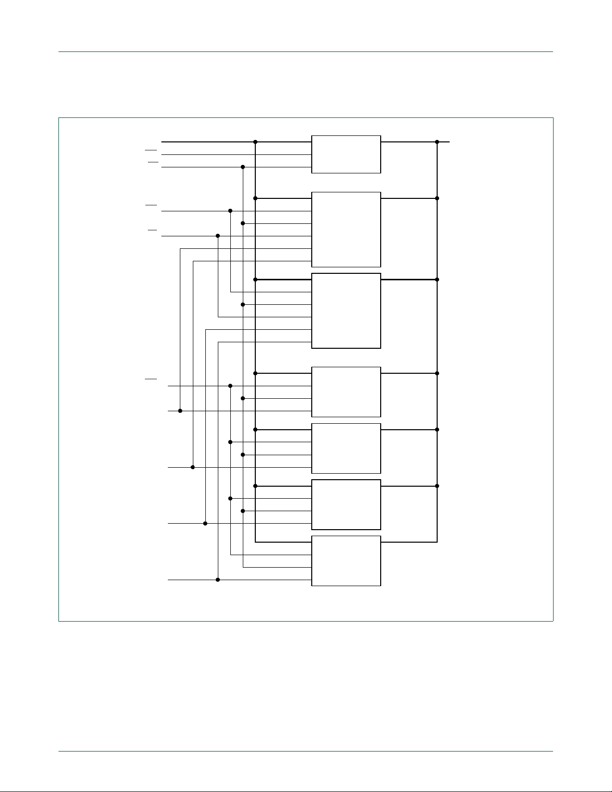
NXP Semiconductors
nCE
nOE
Q[31:0]A[20:0]
nCE
nOE
IO[15:0]A[15:0]
nWE
nUB
nLB
nCE
nOE
IO[15:0]A[15:0]
nWE
nUB
nLB
nCE
nOE
IO[7:0]A[16:0]
nWE
nCE
nOE
IO[7:0]A[16:0]
nWE
nCE
nOE
IO[7:0]A[16:0]
nWE
nCE
nOE
IO[7:0]A[16:0]
nWE
2Mx32 Burst Mask ROM
64Kx16 SRAM, two off
128Kx8 SRAM, four off
A[20:0]
A[20:0]
D[31:0]
D[31:0]
CS0
OE
CS1
CS2
WE
BLS3
BLS2
BLS1
BLS0
A[16:0]
A[16:0]
A[16:0]
A[16:0]
A[15:0]
A[15:0]
D[31:16]
D[15:0]
D[31:24]
D[23:16]
D[15:8]
D[7:0]
11.4 Memory configuration example
UM10237
Chapter 5: LPC24XX External Memory Controller (EMC)
Fig 19. Typical memory conf iguration diagram
UM10237_2 © NXP B.V. 2008. All rights reserved.
User manual Rev. 02 — 19 December 2008 99 of 792
Page 100

UM10237
Chapter 6: LPC24XX Memory Accelerator Module (MAM)
Rev. 02 — 19 December 2008 User manual
1. How to read this chapter
The Memory Accelerator Module operates in combination with the flash controller and is
available in parts LPC2458/68/78.
2. Introduction
The MAM block in the LPC2400 maximizes the performance of the ARM processor when
it is running code in Flash memory using a single Flash bank.
3. Operation
Simply put, the Memory Accelerator Module (MAM) attempts to have the next ARM
instruction that will be needed in its latches in time to prevent CPU fetch stalls. The
LPC2400 uses one bank of Flash memory, compared to the two banks used on
predecessor devices. It includes three 128 bit buffers called the Prefetch buffer, the
Branch Trail Buf fer and the data b uffer. When an Instruction Fetch is not satisfied by either
the Prefetch or Branch Trail buf fe r, nor has a prefetch been initiated for that line, the ARM
is stalled while a fetch is initiated for the 128 bit line. If a prefetch has been initiated but not
yet completed, the ARM is stalled for a shorter time. Unless aborted by a data access, a
prefetch is initiated as soon as the Flash has completed the previous access. The
prefetched line is latched by the Flash module, but the MAM does not capture the line in
its prefetch buffer until the ARM core present s the address from which the prefetch has
been made. If the core presents a different address from the one from which the prefetch
has been made, the prefetched line is discarded.
The prefetch and Branch Trail buffers each include four 32 bit ARM instructions or eight
16 bit Thumb instructions. During sequential code execution, typically the prefetch buffer
contains the current instruction and the entire Flash line that contains it.
The MAM uses the LPROT[0] line to differentiate between instructio n an d data accesses.
Code and data accesses use separate 128 bit buffers. 3 of every 4 sequential 32 bit code
or data accesses "hit" in the buffer without requiring a Flash access (7 of 8 sequential
16 bit accesses, 15 of every 16 sequential byte accesses). The fourth (eighth, 16th)
sequential data access must access Flash, aborting any prefetch in progress. When a
Flash data access is concluded, any prefetch that had been in progress is re-initiated.
Timing of Flash read operations is programmable and is described later in this section.
In this manner , there is no code fetch penalty for sequential instruction execution when the
CPU clock period is greater than or equal to one fourth of the Flash access time. The
average amount of time spent doing program bra nches is relatively small (less than 25%)
and may be minimized in ARM (rather than Thumb) code through the use of the
conditional execution feature present in all ARM instructions. This conditional execution
may often be used to avoid small forward branches that would otherwise be necessary.
UM10237_2 © NXP B.V. 2008. All rights reserved.
User manual Rev. 02 — 19 December 2008 100 of 792
 Loading...