

Page 1
User’s Manual
924-75300
Rev 1
April 8, 2004
EVB912UF32
Evaluation Board
User’s Manual
© Motorola, In c., 2004
Page 2

Important Notice to Users
While every effort has been made to ensure the accuracy of all information in
this document, Motorola assumes no liability to any party for any loss or
damage caused by errors or omissions or by statements of any kind in this
document, its updates, supplements, or special editions, whether such errors are
omissions or statements resulting from negligence, accident, or any other cause.
Motorola further assumes no li ability arising out of the application or use of any
information, product, or system described herein: nor any liability for incidental
or consequential damages arising from the use of this document. Motorola
disclaims all warranties regarding the information contained herein, whether
expressed, implied, or statutory, including implied warranties of
merchantability or fitness for a particular purpose. Motorola makes no
representation that the interconnection of products in the manner described
herein will not infringe on existing or future patent rights, nor do the
descriptions contained herein imply the granting or license to make, use or sell
equipment constructed in accordance with this description.
Trademarks
This document includes these trademar ks:
Motorola and the Motorola logo are registered trademarks
of Motorola, Inc.
Windows is a registered trademark of Microsoft Corporation in the U.S.
and other countries.
Intel is a registered trademark of Intel Corporation.
Motorola, Inc., is an Equal Opportunity / Affirmative Action Employer.
© Motorola, Inc., 2004, All Rights Reserve d
EVB912UF32 Evaluation Board - Rev 1 User’s Manual
2 MOTOROLA
Page 3

Table of Contents
Section 1 General Inform a tion
1.1 Descr i p t i o n . . . . . . . . . . . . . . . . . . . . . . . . . . . . . . . . . . . . . . . . . . . . . . 3
1.2 Features. . . . . . . . . . . . . . . . . . . . . . . . . . . . . . . . . . . . . . . . . . . . . . . . . 3
1.3 Syste m Re q u i rements . . . . . . . . . . . . . . . . . . . . . . . . . . . . . . . . . . . . . . 4
1.4 EVB912UF32 Layout. . . . . . . . . . . . . . . . . . . . . . . . . . . . . . . . . . . . . . 5
1.5 Specifications . . . . . . . . . . . . . . . . . . . . . . . . . . . . . . . . . . . . . . . . . . . . 6
Section 2 Configuration and Operation
2.1 Introduction. . . . . . . . . . . . . . . . . . . . . . . . . . . . . . . . . . . . . . . . . . . . . . 7
2.2 Board Configuration Components . . . . . . . . . . . . . . . . . . . . . . . . . . . . 7
2.2.1 Switch e s. . . . . . . . . . . . . . . . . . . . . . . . . . . . . . . . . . . . . . . . . . . . . . 7
2.2.2 Mode Jump ers (W13, W 1 6 , a n d W1 8 ) . . . . . . . . . . . . . . . . . . . . . . 7
2.2.3 Config u ration Ju mper Set tings . . . . . . . . . . . . . . . . . . . . . . . . . . . . 8
2.3 Operat io n . . . . . . . . . . . . . . . . . . . . . . . . . . . . . . . . . . . . . . . . . . . . . . . 9
2.3.1 Functional B lo ck Diagra m. . . . . . . . . . . . . . . . . . . . . . . . . . . . . . . . 9
2.3.2 Memory Map . . . . . . . . . . . . . . . . . . . . . . . . . . . . . . . . . . . . . . . . . 10
2.3.3 USB Inte rface. . . . . . . . . . . . . . . . . . . . . . . . . . . . . . . . . . . . . . . . . 11
2.4 Using Th e Bo ard Connectors . . . . . . . . . . . . . . . . . . . . . . . . . . . . . . . 11
2.5 Using the Me m o ry Cards . . . . . . . . . . . . . . . . . . . . . . . . . . . . . . . . . . 12
Section 3 Support Informati on
3.1 Introduction. . . . . . . . . . . . . . . . . . . . . . . . . . . . . . . . . . . . . . . . . . . . . 15
3.2 Top CompactFlash Connector . . . . . . . . . . . . . . . . . . . . . . . . . . . . . . 15
3.3 ATA Connector. . . . . . . . . . . . . . . . . . . . . . . . . . . . . . . . . . . . . . . . . . 19
3.4 Secure D i g it al Conne c t o r . . . . . . . . . . . . . . . . . . . . . . . . . . . . . . . . . . 21
3.5 Smart Me d i a Connector. . . . . . . . . . . . . . . . . . . . . . . . . . . . . . . . . . . . 22
3.6 Memory S t i c k Co n n e c t o r . . . . . . . . . . . . . . . . . . . . . . . . . . . . . . . . . . 24
User’s Manual EVB912UF32 Evaluation Board - Rev 1
MOTOROLA 1
Page 4

3.7 Background Debug Header. . . . . . . . . . . . . . . . . . . . . . . . . . . . . . . . . 25
3.8 UART Con n e ctor . . . . . . . . . . . . . . . . . . . . . . . . . . . . . . . . . . . . . . . . 26
3.9 USB Conn ector. . . . . . . . . . . . . . . . . . . . . . . . . . . . . . . . . . . . . . . . . . 27
3.10 Breakout Headers . . . . . . . . . . . . . . . . . . . . . . . . . . . . . . . . . . . . . . . . 27
Section 4 Troubleshooti ng
4.1 Descr i p t i o n . . . . . . . . . . . . . . . . . . . . . . . . . . . . . . . . . . . . . . . . . . . . . 33
4.2 Common Issues. . . . . . . . . . . . . . . . . . . . . . . . . . . . . . . . . . . . . . . . . . 33
4.2.1 Syste m +5 V PWR LED is n o t lit. . . . . . . . . . . . . . . . . . . . . . . . . . 33
4.2.2 BDM communications are not working. . . . . . . . . . . . . . . . . . . . . 33
4.2.3 The ATA is non-functional . . . . . . . . . . . . . . . . . . . . . . . . . . . . . . 34
4.2.4 Top CompactFlash J11 is non-functional . . . . . . . . . . . . . . . . . . . 34
4.2.5 Bottom CompactFlash J13 is non-functional. . . . . . . . . . . . . . . . . 34
4.2.6 The SD/MMC, Memory Stick, or SmartMedia is non-functional. 35
4.2.7 The USB 2.0 Interface is non-functional . . . . . . . . . . . . . . . . . . . . 35
4.2.8 The RS-232 Communication is non-function . . . . . . . . . . . . . . . . 35
EVB912UF32 Evaluation Board - Rev 1 User’s Manual
2 MOTOROLA
Page 5

List of Tables
1-1 Specifi c ations. . . . . . . . . . . . . . . . . . . . . . . . . . . . . . . . . . . . . . . . . . . . 6
2-1 Switch e s. . . . . . . . . . . . . . . . . . . . . . . . . . . . . . . . . . . . . . . . . . . . . . . . 7
2-2 Boot Mo d e J u m p er Settin g s. . . . . . . . . . . . . . . . . . . . . . . . . . . . . . . . . 8
2-3 Config u ration Ju mper Set tings . . . . . . . . . . . . . . . . . . . . . . . . . . . . . . 8
2-4 EVB912UF32 Connectors . . . . . . . . . . . . . . . . . . . . . . . . . . . . . . . . . 11
3-1 CompactFlash Connector J11 & J13 Signal Descriptions. . . . . . . . . 18
3-2 ATA Connector J2 Si g n a l D escriptions. . . . . . . . . . . . . . . . . . . . . . . 20
3-3 Secure Digital Connector J17 Signal Descriptions . . . . . . . . . . . . . . 22
3-4 SmartMedia Connec t o r J7 Signal D e scripti o n s. . . . . . . . . . . . . . . . . 2 3
3-5 Memory Stick Connector J19 Signal Descriptions. . . . . . . . . . . . . . . 25
3-6 J3 Background Debug Header Signal Descriptions . . . . . . . . . . . . . . 25
3-7 Connec t o r J31 Signa l D e script io n s . . . . . . . . . . . . . . . . . . . . . . . . . . 26
3-8 USB Connector J5 Signal Descriptions. . . . . . . . . . . . . . . . . . . . . . . 27
3-9 J4 Breako ut Hea d er S i g n a l De sc riptio n s. . . . . . . . . . . . . . . . . . . . . . 28
3-10 J9 Breakout Header Signal Descriptions . . . . . . . . . . . . . . . . . . . . . . 29
3-11 J10 Breakout Head er Signal D e scripti o n s . . . . . . . . . . . . . . . . . . . . . 30
3-12 J12 Breakout Head er Signal D e scripti o n s . . . . . . . . . . . . . . . . . . . . . 31
3-13 J16 Breakout Head er Signal D e scripti o n s . . . . . . . . . . . . . . . . . . . . . 32
User’s Manual EVB912UF32 Evaluation Board - Rev 1
MOTOROLA 1
Page 6

EVB912UF32 Evaluation Board - Rev 1 User’s Manual
2 MOTOROLA
Page 7

List of Figures
1-1 EVB912UF32 Board Layout. . . . . . . . . . . . . . . . . . . . . . . . . . . . . . . . 5
2-1 Functi o n a l Blo ck Diagram. . . . . . . . . . . . . . . . . . . . . . . . . . . . . . . . . 10
3-1 Top CompactFlash Conn e c t o r J 11 Pi n As si g n m e n t s. . . . . . . . . . . . . 16
3-2 Bottom CompactFlash Connector J13 Pin Assignments. . . . . . . . . . 17
3-3 ATA Conn e c t o r J2 Pi n A ssignments. . . . . . . . . . . . . . . . . . . . . . . . . 20
3-4 Secure Digital Connector J17 Pin Assignments . . . . . . . . . . . . . . . . 22
3-5 SmartMedia Co n n e ct o r J7 Pin Assignment s . . . . . . . . . . . . . . . . . . . 2 3
3-6 Memory Stick Connector J19 Pin Assignments . . . . . . . . . . . . . . . . 24
3-7 J3 Background Debug Header Pin Assignments . . . . . . . . . . . . . . . . 25
3-9 USB Connector J5 Pin Assignments . . . . . . . . . . . . . . . . . . . . . . . . . 27
3-10 J4 Breako ut Header Pin As si g n m e n t s . . . . . . . . . . . . . . . . . . . . . . . . 28
3-11 J9 Breako ut Header Pin As si g n m e n t s . . . . . . . . . . . . . . . . . . . . . . . . 29
3-12 J10 Bre akout Header Pin As si g n m e n t s . . . . . . . . . . . . . . . . . . . . . . . 30
3-13 J12 Bre akout Header Pin As si g n m e n t s . . . . . . . . . . . . . . . . . . . . . . . 31
3-14 J16 Bre akout Header Pin As si g n m e n t s . . . . . . . . . . . . . . . . . . . . . . . 32
User’s Manual EVB912UF32 Evaluation Board - Rev 1
MOTOROLA 1
Page 8

EVB912UF32 Evaluation Board - Rev 1 User’s Manual
2 MOTOROLA
Page 9

User’s Manual — EVB912UF32
1.1 Description
This user’s manual explains how to connect and operate the Motorola
EVB912UF32 Evaluation Board (EVB).
This board is a development tool which allows the user to run software
applications for MC9S12UF32 microcontroller unit (MCU).
The EVB912UF32 includes connectors for CompactFlash, SmartMedia, Secure
Digital/Multimedia, and Memory Stick cards as well as a standard 40 pin ATA
interface. The system also features a USB 2.0 interface. The board has several
20-pin headers that are connected to most of the processors signals. These
provide convenient points to observe these signals or connection points for
external user designed circuit boards.
General Information
Description
Section 1 General Information
1.2 Features
The EVB912UF32 features include:
• MC9S12UF32 MCU
• 12 MHZ crystal with an option to use an externally generated clock
connected to the on board BNC, J1, or a user provided crystal oscillator
plugged into the socket for Y2
• Voltage regulator with an ON/OFF switch and a fused input that steps
down a nominal 12.0-volt input from an ex ternal power supply to 5 volt
power
• Two Type II CompactFlash connectors with software selectable 5 volt or
3.3 volt power
• Secure Digital/MultiMediaCard connector (SD/MMC)
• SmartMedia connector
User’s Manual EVB912UF32 Evaluation Board Rev 1
MOTOROLA General Information 3
Page 10

General Information
• Memory Stick connector
• ATA Interface connector
• One UART port with RS232 transceiver and DB9 connector
• Background Debug Mode (BDM) connector
• USB 2.0 interface and series B USB connector
• Break out headers for all processor control signals
• Power On Reset and a push button reset functions
• Input power and CompactFlash card power status LEDs
• Four user definable LEDs that can be disconnected from their control
signals
• Universal power supply with 12.0-volt output @1200ma
• PC compatible USB 2.0 cable
• A Multilink BDM w/ USB interface connection
• Metrower ks CodeWarrior IDE software (evaluation copy)
1.3 System Requirements
To use an EVB912UF32 Application Development System, you need:
• An IBM PC or compatible computer that has:
– a Windows 98, Windows ME, Windows XP, Windows 2000,
– A Multilink BDM module or compatible device
•A +9 to +15 volt power supply, at 500mA, with a 2 mm female (inside
positive) power connector (included).
CAUTION: Never supply more than +15-volts power to your EVB912UF32. Doing so could
damage board components.
or Windows NT (version 4.0) operating system.
EVB912UF32 Evaluation Board - Rev 1 User’s Manual
4 General Information MOTOROLA
Page 11
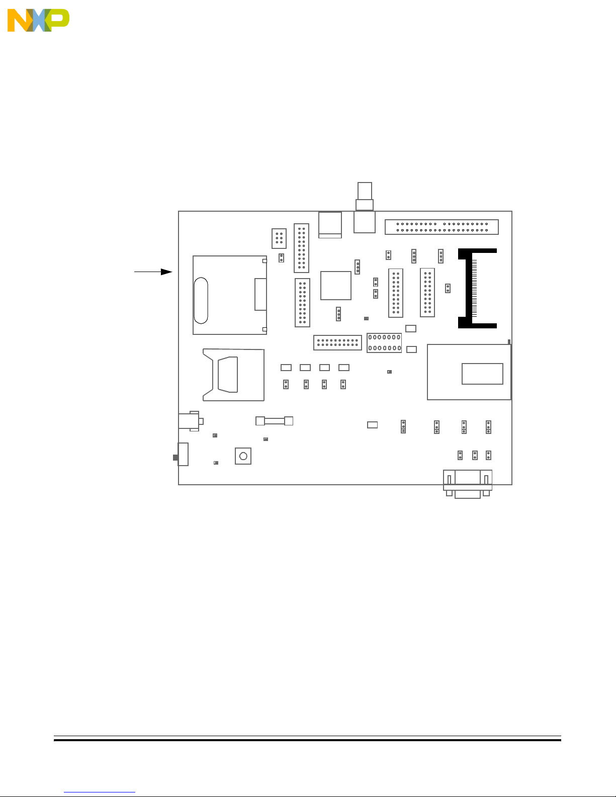
1.4 EVB912UF32 Layout
Figure 1-1 shows the layout of the EVB912UF32. This may be useful in
locating configuration jumpers and connectors. Note that a second
CompactFlash connector, J13, is located on the opposite side of the board.
J13
BOTTOM SIDE
CompactFlash
SMART MEDIA J7
J3 J4
BDM
J6
J12
General Information
EVB912UF32 Layout
J5 USB
J1 EXT
CLK
W1
W2
J9
W5
J2 ATA
W3 W4
J10
W6
J11
U5
J16
Secure Digital J17
DS3 DS5 DS6DS4
LED4
LED3W8LED2W9LED0
W7
J20
ON
OFF
+12V IN
J21
+5V
S1
J23
GND
S2
RESET
F1
1.5A
J22
+12V
Figure 1-1 EVB912UF32 Board Layout
Important board components are:
W19
W10
J8
J15
GND
Y2
J18
+3.3V
EVB912UF32
RE11198B Rev
DS7
+5V PWR
VREGEN
W11
DS1
5V
DS2
3.3V
COMPACT
FLASH POWER
MEMORY STICK
J19
W13
MODC
COMPAC T FLASH
W18
MODB
J31 DCE
W16
MODA
W17W15W14
• U1 — MC9S12UF32 MCU
• J1 — External Clock connector
• J2 — ATA Interface connector
• J3 — BDM connector
• J4, J9, J10, J12, J16 — Signal break out headers
User’s Manual EVB912UF32 Evaluation Board Rev 1
MOTOROLA General Information 5
Page 12

General Information
• J5 — USB connector (type B)
• J7 —SmartMedia connector
• J11, J13 — CompactFlash connectors
• J17 — SD/MMC connector
• J19 — Memory Stick connector
• J31 — RS232 serial interface connector
• S1 — Power switch
• S2 — Reset switch
• DS1 — +5 volt to CF/ATA connectors LED (red)
• DS2 — +3.3 volt to CF/ATA connectors LED (green)
• DS3, DS4, DS5, and DS6 — User definable status LEDs (amber)
• DS7 — +5 volt power ON LED (green)
1.5 Specifications
Characteristic Specifications
Clock speed 12 MegaHertz
Ports USB 2.0, RS-232 serial
Temperature
operating
storage
Relative humidity 0 to 90% (noncondensing)
Power requirements 9.0V
Dimensions 5.5 x 6.5 inches (14 x 16.6centimeters)
Table 1-1 lists EVB912UF32 specifications.
Table 1-1 Specifications
-10° to +50° C
-40° to +85° C
— 15.0 VDC at .5 A
EVB912UF32 Evaluation Board - Rev 1 User’s Manual
6 General Information MOTOROLA
Page 13
User’s Manual — EVB912UF32
Section 2 Configuration and Operation
2.1 Introduction
This section consists of configuration information, connection descriptions, and
other operational information that may be useful in your development activities.
2.2 Boar d Configuration C omponents
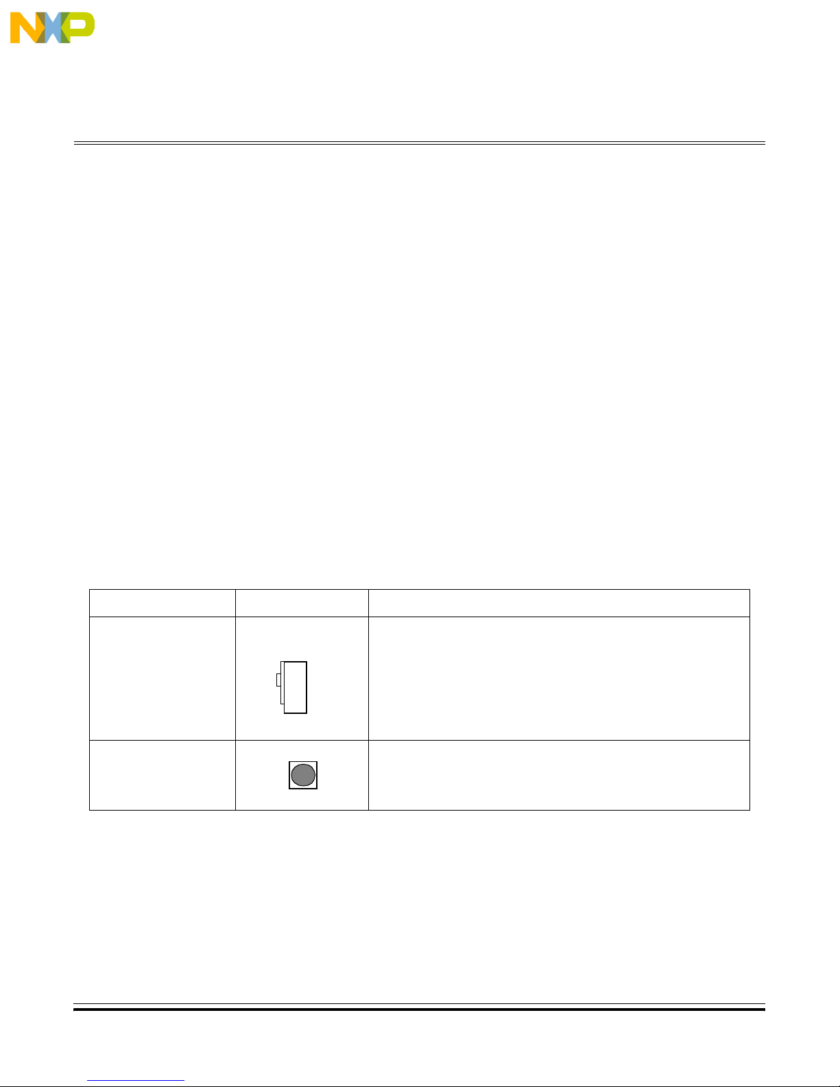
2.2.1 Switches
Table 2-1 is a summary of the switches of the EVB912UF32.
Table 2-1 Switches
Component Position Effect
System Power
Switch, S1
System Reset Swi tch,
S2
ON
S1
OFF
S2
Move this switch to the ON position to enable the power
source connected to J20 to power the system.
Factory setting is OFF.
Push to reset the MC9S12UF32.
2.2.2 Mode Jumpers (W13, W16, and W18)
Jumpers W13, W16, and W18 allow the user to configure the boot mode. The
selection takes effect only on power up or after a reset is applied.
User’s Manual EVB912UF32 Evaluation Board Rev 1
MOTOROLA Configuration and Operation 7
Page 14

Configuration and Operation
Table 2-2 lists settings for the boot-mode jumpers. Place the jumper between
pins 1 and 2 to select a HI (logic 1) and between pins 2and 3 to select a LOW
(logic zero).
.
Table 2-2 Boot Mode Jumper Sett ings
Special Single Chip LOW LOW LOW
Emulation Expanded Narrow LOW LOW HI
Special Test (Expanded Wide) LOW HI LOW
Emulation Expanded Wide LOW HI HI
Normal Single Chip (Factory setting) HI LOW LOW
Normal Expanded Narrow HI LOW HI
Special Peripheral HI HI LOW
Normal Expanded Wide HI HI HI
2.2.3 Configuration Jumper Settings
Table 2-3 lists the functions controlled by the rest of the jumpers on the board.
Tab le 2-3 Configuration Jumper Settings
Function/RefDes Setting/ pins Effect
CLK / W1 XTAL 1-2* Selects crystal operation
TERM / W2 JUMPR IN* Connects a 49 ohm termination to
RST / W3 RST_B 1-2 Connects an active LOW reset to the
CSEL / W4 HI 1-2 CSEL is connected to VDDX
RXD / W5 JUMPR IN* CF_A5 controls RS232 Received
TXD / W6 JUMPR IN* Connects RS232 Transmitted Data to
W13
Boot Mo de
OSC 2-3 Selects Y2 oscillator or an external
oscillator through J1
the external clock line
JUMPR OUT 49 ohm termination is not connected
CompactFlash reset, CF_RES
RST 2-3* Connects an active HI reset to the
CompactFlash reset, CF_RES
LOW 2-3* CSEL is connected to Ground
Data.
JUMPR OUT CF_A5 is disconnected from RS232
Received Data.
CF_A6.
MODC
W18
MODB
MODA
W16
EVB912UF32 Evaluation Board- Rev 1 User’s Manual
8 Configuration and Operation MOTOROLA
Page 15

Configuration and Operation
Operation
Tab le 2-3 Configuration Jumper Settings
Function/RefDes Setting/ pins Effect
JUMPR OUT CF_A6 is disconnected from RS232
Transmitted Data.
EN3 / W7 JUMPR IN* Enables LED3 (DS3) to be controlled
by PT3
JUMPR OUT Disconnects LED3 (DS3) from PT3
EN2 / W8 JUMPR IN* Enables LED2 (DS4) to be controlled
by PT2
JUMPR OUT Disconnects LED2 (DS4) from PT2
EN1 / W9 JUMPR IN* Enables LED1 (DS5) to be controlled
by PT1
JUMPR OUT Disconnects LED1 (DS5) from PT1
EN0 / W10 JUMPR IN* Enables LED0 (DS6) to be controlled
by PT0
JUMPR OUT Disconnects LED0 (DS6) from PT0
VREGEN / W11 ENBL 1-2* Enables internal voltage regulators.
DISBL 2-3 Disables internal voltage regulators.
DSR- DTR/ W14 JUMPR IN* Connects DSR to DTR at J31
JUMPR OUT DSR and DTR are not connected
RST - CTS/ W15 JUMPR IN* Connect RST to CTS at J31
JUMPR OUT RST and CTS are not connected
DCD- DTR/ W17 JUMPR IN* Connect DCD to DTR at J31
JUMPR OUT DCD and DTR are not connected
VDD3X SEL/ W19 P3_3V 1-2* 3.3V power connects to VDD3X
VDDX 2-3 VDDX power connects to VDD3X
* These are the fac tory sett ings.
2.3 Operation
This section contains designed to help the user understand how to use the board
and how the system functions.
2.3.1 Functional Block Diagram
Figure 2-1 is a block diagram of the EVB912UF32 system. Please note that not
all interface signals are called out. The signals ending with "x" represent a group
of signals that begin with the same letter(s) that proceed the "x".
User’s Manual EVB912UF32 Evaluation Board - Rev 1
MOTOROLA Configuration and Operation 9
Page 16

Configuration and Operation
J5
External
Clock
J1
J3
+12V
USB
2.0
OSC
Clock
BDM
Reset
MOD
J4
Power
Supply
EN
MC9S12UF32
VDDA
VDDR VDD3X
+5V
VDDX
REF_3V
PWR3VOFF
PWR5VOFF
Q1
CFATA_x
CFA(3..10)
PT(0..3)
Status
LEDs
SDx
MSx
Sx
+3.3V
Voltage
Select
J10
CFA6
CFA5
W19
ATA
TERMS
J9
W5/W6
VDDX
J16
J12
ATA
Top
Compact
Flash
RS-232
Bottom
Compact
Flash
SD/MMC
Memory
Stick
Smart
Media
J2
J11
J31
J13
J17
J19
J7
Figure 2-1 Functional Block Diagram
2.3.2 Memory Map
The EVB912UF32 does not have an external memory bus. All system
peripherals are internal to the microprocessor. Please re fer to the specification
for the MC9S12UF32 to get memory map information.
EVB912UF32 Evaluation Board- Rev 1 User’s Manual
10 Configuration and Operation MOTOROLA
Page 17

2.3.3 USB Interface
The USB Device Module of the MC9S12UF32 connects directly to
a USB type B connector, J5. For details on the operation of the
USB interface, please refer to the MC9S12UF32 data sheet.
2.4 Using The Board Connectors
Table 2-4 lists the EVB912UF32 connectors, explaining their function, and
any special instructions for using the connector.
Table 2-4 EVB912UF32 Connectors
Connector Purpose Comments
J1 External Clock Connector for inputting a system clock from and external
source such as a waveform generator. Provides a standard
BNC connection. Input clock must be <= +5 volts.
Configuration and Operation
Using The Board Connectors
J2 ATA5 Connector for standard 40 conductor ATA ribbon cable .
Shares signals with the top side CompactFlash connector.
J3 BDM Background debug connector, 6 pin version. Compatible with
the Multilink BDM produced by P&E Microcomputer Systems.
J4 Break Out Mainly USB, power control, configuration, and control signals
J5 USB Connector for USB 2.0 interface
J6 VDDR current
measurement
connector
J7 SmartMedia Connector for plugging in SmartMedia compatible memory
J8 VDDX current
measurement
connector
J9 Break Out Mainly CompactFlash and ATA5 signals.
J10 Break Out Mainly CompactFlash and ATA5 signals.
J11 CompactFlash
(top side)
Jumper to enable in circuit measurement of the current
consumed by the processor from the VDDR source. Remove
the jumper and place an ammeter in line between the posts to
measure the current.
cards.
Jumper to enable in circuit measurement of the current
consumed by the processor from the VDDX source. Remove
the jumper and place an ammeter in line between the posts to
measure the current.
Connector for a standard Type II CompactFlash card. Shares
connections with the ATA connector.
J12 Break Out Mainly SmartMedia signal connections .
User’s Manual EVB912UF32 Evaluation Board - Rev 1
MOTOROLA Configuration and Operation 11
Page 18

Configuration and Operation
Table 2-4 EVB912UF32 Connectors (Continued)
Connector Purpose Comments
J13 CompactFlash
(bottom side)
J15, J23 GND Ground test point connections.
J16 Break Out Mainly SD/MMC and Memory Stick signals
J17 SD/MMC Connector for plugging in SD/MMC compatible memory cards.
J18 3.3V 3.3 volt test point
J19 Memory Stick Connector for standard Memory Stick memory cards. Slide the
J20 Power Connector for nominal +12V input power. Jack is center
J21 5V 5 volt test point
J22 12V 12 volt test point (input power)
J24 REC2_IN Unused RS-232 receiver output
J25 TR2_OUT Unused RS-232 transmitter output
J26 V- Negative RS-232 voltage test point
J27 V+ Positive RS-232 voltage test point
Connector for a standard Type II CompactFlash card. Shares
connections with SD/MMC, Memory Stick, and SmartMedia
connectors.
memory stick into the connector until it snaps into place.
positive.
J28 REC2_OUT Unused RS-232 receiver input
J29 TR2_IN Unused RS-232 transmitter input
J30 RI Ring Indicator pin of RS-232 connector (J31)
J31 RS232 DCE Connector for RS232 interface using RXD and TXD only.
Jumpers can be used to looped back RS232 control signals to
each other.
2.5 Using the Memo ry Cards
The users must obtain their own compatible cards for use with these connectors.
Please note the power for most of these cards is connected to P3.3V which is
+3.3 volts. The CompactFlash (CF) connectors are power by VDDX that can
switch between zero volts, +3.3 volts and +5 volts under software control. W19
selects power to the control signals of all memory card connectors except J11
(the top side CF). VDDX always powers the control signals to J11. The user
EVB912UF32 Evaluation Board- Rev 1 User’s Manual
12 Configuration and Operation MOTOROLA
Page 19

Configuration and Operation
Using the Memory Cards
must exercise caution not to select VDDX when using the SD/MMC, Memory
Stick, or SmartMedia cards. Use W19 to select VDDX as the power source for
VDD3X when using the bottom side CompactFlash, J13. Some of the signals
on J13 are directly powered by VDDX and the rest are referenced to VDD3X.
Caution: W19 must not select VDDX for VDD3X power when using the
SD/MMC, Memory Stick, or SmartMedia cards.
Caution: To avoid circuit damage, do not plug in SmartMedia, SD/MMC, or
Memory Stick cards with power applied to the board.
User’s Manual EVB912UF32 Evaluation Board - Rev 1
MOTOROLA Configuration and Operation 13
Page 20

Configuration and Operation
EVB912UF32 Evaluation Board- Rev 1 User’s Manual
14 Configuration and Operation MOTOROLA
Page 21

User’s Manual — EVB912UF32
3.1 Introduction
This section consists of connector pin assignments, connector signal
descriptions, and other information that may be useful in your development
activities. For the ATA and memory card interfaces, signals described as
outputs are signals that originate from the external device. Input signals
originate on the board going to the device.
3.2 Top CompactFlash Connector
Connector J11 is one of two CompactFlash connectors on the EVB912UF32.
This connector shares signals with the ATA connector, J2, so these connectors
cannot be used at the same time. To use a CompactFlash card and the ATA
interface simultaneously, use the bottom CompactFlash connector, J13. Note
that when using J13, W19 should select VDDX as the VDD3X power source.
Section 3 Support Information
Figure 3-1 gives pin assignments for the top CF connector, J11. Figure 3-2
gives pin assignments for the bottom CF connector. The signal names match the
names used in the schematic and may not be the signal name normally
associated with CompactFlash. Table 3-1 gives signal descriptions for these
connectors. The signal names on the table might not match the schematic or the
figures. Instead they show the intended CompactFlash function that must be
selected for that particular pin.
User’s Manual EVB912UF32 Evaluation Board - Rev 1
MOTOROLA Support Information 15
Page 22

Support Informati on
1
26
25
50
J11
GND 1 • • 26 CF_CD1_B
CFATA_D3 2 • • 27 CFATA_D11
CFATA_D4 3 • • 28 CFATA_D12
CFATA_D5 4 • • 29 CFATA_D13
CFATA_D6 5 • • 30 CFATA_D14
CFATA_D7 6 • • 31 CFATA_D15
CE1_CS0 7 • • 32 CE2_CS1
CF_A10 8 • • 33 VS1
CFOE_B 9 • • 34 CFATA_IORD
CF_A9 10 • • 35 CFATA_I OWR
CF_A8 11 • • 36 WE_DMARQ
CF_A7 12 • • 37 RDY_INT
VDDX 13 • • 38 VDDX
CF_A6 14 • • 39 CSEL
CF_A5 15 • • 40 NC
CF_A4 16 • • 41 CF_RES
CF_A3 17 • • 42 WAIT_IORDY
CFATA_A2 18 • • 43 IPAC_DMAC
CFATA_A1 19 • • 44 CF_REG_B
CFATA_A0 20 • • 45 NC
CFATA_D0 21 • • 46 B VD1_DASP
CFATA_D1 22 • • 47 CFATA_D8
CFATA_D2 23 • • 48 CFATA_D9
CFIOIS16 24 • • 49 CFATA_D10
CF_CD2_B 25 • • 50 GND
Figure 3-1 Top CompactFlash Connector J11 Pin Assignments
EVB912UF32 Evaluation Board- Rev 1 User’s Manual
16 Support Information MOTOROLA
Page 23

Support Information
Top CompactFlash Connector
50
25
J13
GND 1 • • 26 CF_CD1_B
SDAT3 2 • • 27 SWP
SDAT4 3 • • 28 SCLE
SDAT5 4 • • 29 SALE
SDAT6 5 • • 30 SWE
SDAT7 6 • • 31 SRE
MSSDTO 7 • • 32 MSSCLK
CF_A10 8 • • 33 VS1
CFOE_B 9 • • 34 SDDATA 3
CF_A9 10 • • 35 MSBS
CF_A8 11 • • 36 PT3
CF_A7 12 • • 37 SDCMD
VDDX 13 • • 38 VDDX
CF_A6 14 • • 39 CSEL
CF_A5 15 • • 40 NC
CF_A4 16 • • 41 CF_RES
CF_A3 17 • • 42 SDDATA0
PT2 18 • • 43 SDDATA1
PT1 19 • • 44 SDCLK
PT0 20 • • 45 NC
SDAT0 21 • • 46 B VD1 _DA SP
SDAT1 22 • • 47 SBSY
SDAT2 23 • • 48 SCD
SDDATA2 24 • • 49 SCE
CF_CD2_B 25 • • 50 GND
26
1
Figure 3-2 Bottom CompactFlash Connector J13 Pin Assignments
User’s Manual EVB912UF32 Evaluation Board - Rev 1
MOTOROLA Support Information 17
Page 24

Support Informati on
Table 3-1 CompactFlash Connector J11 & J13 Signal Descriptions
Pin(s)
1,50 GND GROUND
2 D03 DATA BIT 3 — Bidirectional
3 D04 DATA BIT 4— Bidirectional
4 D05 DATA BIT 5 — Bidirectional
5 D06 DATA BIT 6 — Bidirectional
6 D07 DATA BIT 7 — Bidirectional
7CE1
8 A010 ADDRESS BIT 10 — Input
9OE
10 A09 ADDRESS BIT 9 — Input
11 A08 ADDRES S BIT 8 — Input
12 A07 ADDRESS BIT 7 — Input
13,38 VCC POWER, Software selectable for +5 or +3.3 volts
14 A06 ADDRESS BIT 6 — Input
15 A05 ADDRESS BIT 5 — Input
16 A04 ADDRESS BIT 4 — Input
17 A03 ADDRESS BIT 3 — Input
18 A02 ADDRESS BIT 2 — Input
19 A01 ADDRESS BIT 1 — Input
20 A00 ADDRESS BIT 0 — Input
21 D00 DATA BIT 0 — Bidirectional
22 D01 DATA BIT 1— Bidirectional
23 D02 DATA BIT 2 — Bidirectional
24 IOIS16
25 CD2
26 CD1
27 D011 DATA BIT 11 — Bidirectional
28 D012 DATA BIT 12 — Bidirectional
29 D013 DATA BIT 13 — Bidirectional
30 D014 DATA BIT 14 — Bidirectional
31 D015 DATA BIT 15 — Bidirectional
32 CE2
33 VS1 VOLTAGE SENS E 1 — Output, groun ded for 3.3V operation
34 IORD
35 IOWR
36 WE
37 RDY /B SY
Function
CARD ENABLE 1 — Active low input
OUTPUT ENABLE — Active low input
I/O OPERATION — Active low output
CARD DETECT 2 — Output, connected to ground inside the card
CARD DETECT 1 — Output, connected to ground inside the card
CARD ENABLE 2 — Active low input
IO READ — Active low input, gates data in I/O mode
IO WRITE —Active low input, clocks data to the CF card
WRITE ENABLE — Active low input, used to write to configuration
registers
READY BUSY— Active low output, Indicates the card is not ready or
could be an interrupt
Description
EVB912UF32 Evaluation Board- Rev 1 User’s Manual
18 Support Information MOTOROLA
Page 25

Support Information
ATA Connector
Pin(s) Function Description
39 CSEL CABLE SELECT — Input, indicates unit is a Master or Slave only in
TRUE IDE mode. Otherwise this signal is not used.
40,45 NC NO CONNETION
41 RE SET RESET— Input, active high except in True IDE mode
42 WAIT
43 INPACK
44 REG
46 BVD1 I/O — Can be a status change indication or a Diagnostic test is
47 D08 DATA BIT 8 — Bidirectional
48 D09 DATA BIT 09— Bidirectional
49 D10 DATA BIT 10 — Bidirectiona l
WAIT — Active low output, indicates the card wants to delay the current
memory access cycle.
INPUT ACKNOWLEDGE - Active low output
REGISTER — Active low input, If used indicates a register access to
the card
complete indication.
3.3 ATA Connector
Connector J2 is a standard ATA 40-pin header connector. Figure 3-3 gives the
pin assignments and Table 3-2 gives the signal descriptions for this connector.
User’s Manual EVB912UF32 Evaluation Board - Rev 1
MOTOROLA Support Information 19
Page 26

Support Informati on
J2
TRESET_B 1 • • 2GND
DD7 3 • • 4 DD8
DD6 5 • • 6 DD9
DD5 7 • • 8 DD10
DD4 9 • • 10 DD11
DD3 11 • • 12 DD12
DD2 13 • • 14 DD13
DD1 15 • • 16 DD14
DD0 17 • • 18 DD15
GND 19 • • 20 KEY
DMARQ 21 • • 22 GND
IOWR_B 23 • • 24 GND
IORD_B 25 • • 26 GND
IORDY 27 • • 28 CSEL
DMACK_B 29 • • 30 GND
INTRQ 31 • • 32 NC
A1 33 • • 34 NC
A0 35 • • 36 A2
CS0_B 37 • • 38 CS1_B
BVD1_DASP 39 • • 40 GND
Figure 3-3 ATA Connector J2 Pin Assignments
Table 3-2 ATA Connector J2 Signal Descriptions
Pin(s)
1 TRESET_B RESET - Active low input
2, 19, 22, 24,
26, 30, 40,
3 DD7 DATA BIT 8— Bidirectional
4 DD8 DATA BIT 8 — Bidirectional
5 DD6 DATA BIT 6— Bidirectional
6 DD9 DATA BIT 9 — Bidirectional
7 DD5 DATA BIT 5 — Bidirectional
8 DD10 DATA BIT 10 — Bidirectional
9 DD4 DATA BIT 4 — Bidirectional
10 DD11 DATA BIT 11 — Bidirectional
11 DD3 DATA BIT 3 — Bidirectional
12 DD12 DATA BIT 12 — Bidirectiona l
13 DD2 DATA BIT 2 — Bidirectional
14 DD13 DATA BIT 13 — Bidirectiona l
15 DD1 DATA BIT 1 — Bidirectional
16 DD14 DATA BIT 14 — Bidirectiona l
Function
GND GR OUND
Description
EVB912UF32 Evaluation Board- Rev 1 User’s Manual
20 Support Information MOTOROLA
Page 27

Secure Digital Connector
Pin(s) Function Description
17 DD0 DATA BIT 0 — Bidirectional
18 DD15 DATA BIT 15 — Bidirectiona l
20 KEY Missing pin to key connector
21 DMARQ Direct Memory Access Request — Active high output
23 IOWR_B Input/Output Write — Active low input
25 IORD_B Input/Output Read — Active low input
27 IORDY Input/Output Ready — Active low output
28 CSEL Cable Select
29 DMACK_B DIrect Memory Access Acknowle dge — Ac tive low input
31 INTRQ Interrupt Request — Active high output
32, 34 NC Not Connec ted
33 A1 ADDRESS BIT 1 — Device address input
35 A0 ADDRESS BIT 0 — Device address input
36 A2 ADDRESS BIT 2 — Device address input
37 CS0_B Chip Select 0 — Active low input
38 CS1_B Chip Select 1 — Active low input
39 BVD1_DASP Device Active or Slave Present — Bidirectional
Support Information
3.4 Secure Digital Connector
Connector J17 is the EVB912UF32 Secure Digital (SD) connector.
Figure 3-4 gives the pin assignments and Table 3-3 gives the signal
descriptions for this connector.
User’s Manual EVB912UF32 Evaluation Board - Rev 1
MOTOROLA Support Information 21
Page 28

Support Informati on
1234567891011 13
12
14
Figure 3-4 Secure Digital Connector J17 Pin Assignments
Table 3-3 Secure Digital Connector J17 Signal Descriptions
Pin(s) Signal
1 SDDATA3 Not Used Data Line DAT3
2 SDCMD Command / Response
3, 6 GND GROUND
4 VCC +3 volt power
5 S DCLK Clock
7 SDDATA0 Data Line DAT0
8 SDDATA1 Interrupt (IRQ) Data Line DAT1 or
9 SDDATA2 Read/Wait (RW) Data Line DAT2 or
10 SD_CD Card Detect
11 GND Card Detect Switch 2
12 SD_WP Write Protect
1-Bit Mode 4-Bit Mode
Description
Inte rr u pt (IRQ)
Read/Wait (RW)
3.5 SmartMedia Connector
Connector J7 is the EVB912UF32 connector for SmartMedia cards. Figure 3-5
gives the pin assignments and Table 3-4 gives the signal descriptions for this
connector.
EVB912UF32 Evaluation Board- Rev 1 User’s Manual
22 Support Information MOTOROLA
Page 29

Support Information
2
2
SmartMedia Connector
2
1
26
25
11
1
Figure 3-5 SmartMedia Connector J7 Pin Assignments
Table 3-4 SmartMedia Connector J7 Signal Descriptions
Pin(s) S ignal Description
1,10,18 GND GROUND
2 SCLE SmartMedia Command Latch Enable — Active
high input
3 SALE SmartMedia Address Latch Enable — Ac tive
high input
4 SWE SmartM edia Write Enable — Active low input
5 SWP SmartM edia Write Protect — Active low input
6 SDAT0 SmartMedia Data Bit 0 — Bidirectional
7 SDAT1 SmartMedia Data Bit 1 — Bidirectional
8 SDAT2 SmartMedia Data Bit 2 — Bidirectional
9 SDAT3 SmartMedia Data Bit 3 — Bidirectional
1 1 SCD SmartMedia Card Detect — Low if card is
present
12,22 P3_3V +3.3 volt power
13 SDAT 4 SmartMedia Data Bit 4 — Bidirectional
14 SDAT 5 SmartMedia Data Bit 5 — Bidirectional
15 SDAT 6 SmartMedia Data Bit 6 — Bidirectional
16 SDAT7 SmartMedia Data Bit 7 — Bidirectional
17 SLVD SmartMedia Low Voltage Detect
19 SBSY SmartMedia Busy — Active low output, open
drain.
20 SRE SmartMedia Read Enable — Active low input
21 SCE SmartMedia Card Enable — Active low input
User’s Manual EVB912UF32 Evaluation Board - Rev 1
MOTOROLA Support Information 23
Page 30

Support Informati on
Table 3-4 SmartMedia Connector J7 Signal Descriptions
Pin(s) S ignal Description
23, 24,
25, 26
3.6 Memory Stick Connector
Connector J19 is the EVB912UF32 connector for Memory Stick cards.
Figure 3-6 gives the pin assignments and Table 3-5 gives the signal descriptions
for this connector.
NC Not Connected — Mechanical support
10
1
Figure 3-6 Memory Stick Connector J19 Pin Assignments
EVB912UF32 Evaluation Board- Rev 1 User’s Manual
24 Support Information MOTOROLA
Page 31

Table 3-5Memory Stick Connector J19 Signal Descriptions
Pin(s) S ignal Description
1,10 GND GROUND
2 MSBS Memory Stick Bus State —Input
3, 9 VCC +3.3 volt power
4 MSSDIO Memory Stick Data Input/Output — Serial data
5,7 NC No Connection
6 MSSINS Memory Stick Insert — Low if card is present
8 MSSCLK Memory Stick Clock — Input
3.7 Background Debug Header
Support Information
Background Debug Header
Background Debug Header Connector J3 is the EVB912UF32 connector for
using serial debug equipment. Figure 3-7 gives the pin assignments and
Table 3-6 gives the signal descriptions for this connector.
J3
BKGD 1 • • 2GND
NC 3 • • 4 RESET_B
NC 5 • • 6P5V
Figure 3-7J3 Background Debu g Header Pin Assignment s
Table 3-6J3 Background Debug Header Signal Descriptions
Pin(s) S ignal Description
1 BKGD Background Debug — Serial Data
2 GND GROUND
3,5 NC Not Connected
4 RESET_B Reset — Active low, bid irectional
6 P 5V +5 volt power
User’s Manual EVB912UF32 Evaluation Board - Rev 1
MOTOROLA Support Information 25
Page 32

Support Informati on
3.8 UART Connector
Connector J31 is the EVB912UF32 RS-232 serial connector. Figure 3-8 gives
the pin assignments and Table 3-7 gives the signal descriptions for this
connector.
D
N
G
9876
C
N
D
R
T
X
R
D
2345
S
S
T
T
C
R
D
D
C
X
D
T
1
J31
R
S
D
Figure 3-8 J31 RS232 Serial Connector Pin Assignments
Table 3-7 Connector J31 Signal Descript i on s
Pin Mnemonic Signal
1 DCD DATA CARRIER DETECT — RS232 output*
2 TXD TRANSMI TT ED DATA — RS232 serial data output signal
3 RXD RECEIVED DATA – RS232 serial data input signal
4 DTR DATA TERMINAL READY — RS232 input*
5 GND GROUND
6 DSR DATA SET READY — RS232 out p ut *
7 RTS READY TO SEND — RS232 input*
8 CTS CLEAR TO SEND — RS232 output*
9 NC Not Connected
* The outputs are not driven or controlled o n this board. Connect DCD to DTR
using W17, DSR to DTR using W14, and CTS to RTS using W15 to have these
outputs driven by these inputs (loopback connections).
EVB912UF32 Evaluation Board- Rev 1 User’s Manual
26 Support Information MOTOROLA
Page 33

3.9 USB Connector
Table 3-8 USB Connector J5 Signal Descriptions
Support Information
USB Connector
Connector J5 is the USB 2.0 connector. Figure 3-9 gives the pin
assignments and Table 3-8 gives the signal descriptions for this
connector.
.
21
34
Figure 3-9 USB Connector J5 Pin Assignments
Pin Mnemonic Signal
1 NC NO CONNECTION
2 D- USB DATA MINUS
3 D+ USB DATA PLUS
4 GND GROUND
3.10 Breakout Headers
The EVB912UF32 has five breakout headers, J4, J9, J10, J12, and J16. The
headers allow easy access to most signals of the MC9S12UF32 as well as power
and ground connections. The user can connect signals together or connect to
circuits on other boards via wire jumpers, wire wrap, or as groups via 20
conductor ribbon cables. The following figures and signal descriptions show the
pin assignments by schematic signal names.
User’s Manual EVB912UF32 Evaluation Board - Rev 1
MOTOROLA Support Information 27
Page 34

Support Informati on
J4
GND 1 • • 2VDD
VRGEN 3 • • 4REF3V
CF_CD 5 • • 6XIRQ_B
BVD1_DASP 7 • • 8IRQ_B
R_W 9 • • 10 VS1
LSTRB 11 • • 12 ECLK
XCLKS 13 • • 14 PW ROFF3V
PWROFF5V 15 • • 16 RESET _B
MODA 17 • • 18 MODB
BKGD 19 • • 20 P5V
Figure 3-10 J4 Breakout Header Pin Assignments
Table 3-9 J4 Breakout Header Signal Descriptions
Pin(s) S ignal Description
1 GND GROUND
2 VDD USB Power
3 VRGEN GROUND
4 REF3V 3 Volt Reference
5 CF_ CD Clock
6 XIRQ_B Fast Interrupt Request to processor
7 BVD1_DASP Device Active or Slave Present — Bidirectional
8 IRQ_B Interrupt Request to processor
9 R_W Read/Write
10 VS1 VOLTAGE SENSE 1 — Output from CF cards
11 LST RB Low Byte Strobe — Output from processor
12 ECLK Internal Bus Clock
13 XCLKS Function was removed, Port E, pin 7
14 PWROFF3V P ower OFF 3 volts — Controls VDDX
15 PWROFF5V P ower OFF 5 volts — Controls VDDX
16 RESET_B Reset — Active Low
17 MODA Mode Bit A — Power up configuration bit
18 MODB Mode Bit B — Power up configuration bit
19 BKGD Background debug pin, shared with MODC
20 P5V +5 volt power
EVB912UF32 Evaluation Board- Rev 1 User’s Manual
28 Support Information MOTOROLA
Page 35

Support Information
Breakout Headers
J9
CFATA_A0 1 • • 2CFATA_A1
CFATA_A2 3 • • 4CF_A3
CF_A4 5 • • 6CF_A5
CF_A6 7 • • 8CF_A7
CF_A8 9 • • 10 CF_A9
CF_A10 11 • • 12 CE1_CS0
CE2_CS1 13 • • 14 CFATA_IORD
CFATA_IOWR 15 • • 16 WE_DMARQ
CFOE_B 17 • • 18 CF_REG_B
CFIOIS16 19 • • 20 GND
Figure 3-11 J9 Breakout Header Pin Assignments
Table 3-10 J9 Breakout Header Signal Descriptions
Pin(s) S ignal Description
1 CFATA_A0 CF & ATA ADDRESS BIT 0
2 CFATA_A1 CF & ATA ADDRESS BIT 1
3 CFATA_A2 CF & ATA ADDRESS BIT 2
4 C F_A3 CF ADDRESS BIT 3
5 C F_A4 CF ADDRESS BIT 4
6 C F_A5 CF ADDRESS BIT 5
7 C F_A6 CF ADDRESS BIT 6
8 C F_A7 CF ADDRESS BIT 7
9 C F_A8 CF ADDRESS BIT 8
10 CF_A9 CF ADDRESS BIT 9
11 CF_A10 CF ADDRESS BIT 10
12 CE 1_CS 0 CF Card Enable 1 or ATA Chip Select 0
13 CE 2_CS 1 CF Card Enable 2 or ATA Chip Select 1
14 CFATA _IORD CF & ATA Input/Output Read
15 CFATA_IOWR CF & ATA Inp ut/Output Write
16 WE_DMARQ CF Write Enable or ATA DMA Request
17 CFOE_B CF Output Enable
18 CF_REG_B CF Register Enable
19 CFI OIS 16 CF Input /Outpu t 16 bit operation
20 GND GROUND
User’s Manual EVB912UF32 Evaluation Board - Rev 1
MOTOROLA Support Information 29
Page 36

Support Informati on
J10
CFATA_D0 1 • • 2CFATA_D1
CFATA_D2 3 • • 4CFATA_D3
CFATA_D4 5 • • 6CFATA_D5
CFATA_D6 7 • • 8CFATA_D7
CFATA_D8 9 • • 10 CFATA_D9
CFATA_D10 11 • • 12 CFATA_D11
CFATA_D12 13 • • 14 CFATA_D13
CFATA_D14 15 • • 16 CFATA_D15
WAIT_IORDY 17 • • 18 IPAC_DMAC
RDY_INT 19 • • 20 VDDX
Figure 3-12 J10 Breakout Header Pin Assignments
Table 3-11 J10 Breakout Header Signal Descriptions
Pin(s) S ignal Description
1 CFATA_D0 CF & ATA DATA BIT 0
2 CFATA_D1 CF & ATA DATA BIT 1
3 CFATA_D2 CF & ATA DATA BIT 2
4 CFATA_D3 CF & ATA DATA BIT 3
5 CFATA_D4 CF & ATA DATA BIT 4
6 CFATA_D5 CF & ATA DATA BIT 5
7 CFATA_D6 CF & ATA DATA BIT 6
8 CFATA_D7 CF & ATA DATA BIT 7
9 CFATA_D8 CF & ATA DATA BIT 8
10 CFATA_D9 CF & ATA DATA BIT 9
11 CFATA_D10 CF & ATA DATA BIT 10
12 CFATA_D11 CF & ATA DATA BIT 11
13 CFATA_D12 CF & ATA DATA BIT 12
14 CFATA_D13 CF & ATA DATA BIT 13
15 CFATA_D14 CF & ATA DATA BIT 14
16 CFATA_D15 CF & ATA DATA BIT 15
17 W AIT_IORDY CF Wait to End I/O or ATA I/O Ready
18 IPAC_DMAC CF Input Acknowledge or ATA DMA Ack
19 RDY_INT CF Ready or ATA Interrupt
20 VDDX CF & ATA POWER 3.3 or 5.0 volt selectable
EVB912UF32 Evaluation Board- Rev 1 User’s Manual
30 Support Information MOTOROLA
Page 37

Support Information
Breakout Headers
J12
P3_3V 1 • • 2SDAT0
SDAT1 3 • • 4SDAT2
SDAT3 5 • • 6SDAT4
SDAT5 7 • • 8SDAT6
SDAT7 9 • • 10 SBSY
PT3 11 • • 12 SLVD
SCD 13 • • 14 S C E
SWP 15 • • 16 SCLE
SALE 17 • • 18 S W E
SRE 19 • • 20 GND
Figure 3-13 J12 Breakout Header Pin Assignments
Table 3-12 J12 Breakout Header Signal Descriptions
Pin(s) S ignal Description
1 P3_3V +3.3 volt power
2 SDAT0 SmartMedia DATA BIT 0
3 SDAT1 SmartMedia DATA BIT 1
4 SDAT2 SmartMedia DATA BIT 2
5 SDAT3 SmartMedia DATA BIT 3
6 SDAT4 SmartMedia DATA BIT 4
7 SDAT5 SmartMedia DATA BIT 5
8 SDAT6 SmartMedia DATA BIT 6
9 SDAT7 SmartMedia DATA BIT 7
10 SBSY SmartMedia Busy
11 PT3 Port T, Pin 3
12 SLVD SmartMedia Low Voltage Detect
13 SCD SmartMedia Card Detect
14 SCE SmartMedia Card Enable
15 SW P SmartMedia Write Protect
16 SCLE S martM edia Com ma nd Latch Enable
17 SA LE SmartMedia Address Latch Enable
18 SW E SmartMedia Write Enable
19 SRE SmartMedia Read Enable
20 GND GROUND
User’s Manual EVB912UF32 Evaluation Board - Rev 1
MOTOROLA Support Information 31
Page 38

Support Informati on
J16
GND 1 • • 2 SDCLK
NC 3 • • 4 P3_3V
SDCMD 5 • • 6 SDDATA0
SDDATA1 7 • • 8SSDDATA2
SDDATA3 9 • • 10 PT3
PT2 11 • • 12 SD_CD
PT1 13 • • 14 PT0
SD_WP 15 • • 16 MSSINS
MSBS 17 • • 18 M SSDIO
MSSCLK 19 • • 20 GND
Figure 3-14 J16 Breakout Header Pin Assignments
Table 3-13 J16 Breakout Header Signal Descriptions
Pin(s) S ignal Description
1 GND GROUND
2 SDCLK Secure Digital Clock
3 NC No Connection
4 P3_3V +3.3 volt power
5 SDCMD Secure Digital Command
6 SDDATA0 Secure Digital DATA BIT 0
7 SDDATA1 Secure Digital DATA BIT 1
8 SDDATA2 Secure Digital DATA BIT 2
9 SDDATA3 Secure Digital DATA BIT 3
10 PT3 Port T, Pin 3
11 PT2 Port T, Pin 2
12 SD_CD Secure Digital Card Detect
13 PT1 Port T, Pin 1
14 SD_WP Secure Digital Write Protect
15 PT0 Port T, Pin 0
16 MSSINS Memory Stick Inserted
17 MSBS Memory Stick Bu s State
18 MSSDIO Memory Stick Data input Output
19 MSSCLK Memory Stick Clock
20 GND GROUND
EVB912UF32 Evaluation Board- Rev 1 User’s Manual
32 Support Information MOTOROLA
Page 39

User’s Manual — EVB912UF32
4.1 Description
This section discusses common operational issues and how to resolve them.
4.2 Common Issues
4.2.1 System +5V PWR LED is not lit
Troubleshooting
Description
Section 4 Troubleshooting
Check the EVB912UF32 for power:
1. Verify the power supply is plugged in and the wall outlet has power.
2. Verify that S1 is in the ON position and the power jack is plugged
securely into J20.
3. Check that voltage is available at J22, the +12V test loop.
4. Check that the fuse, F1, is not open. If it is, replace the fuse.
4.2.2 BDM communications are not working.
Communication with the board through the BDM interface, J3, stops working
or will not work.
1. Verify power is properly applied to the boar d. (See 4.2.1.)
2. Verify a valid clock source is selected at W1. Normally the on board
12MHz crystal will be used which requires W1 pins 1-2 to be jumpered.
3. Verify the external Multi-link device is connected to J3 and powered.
4. Verify there is an active USB connection from the Multi-link to the PC.
User’s Manual EVB912UF32 Evaluation Board Rev 1
MOTOROLA Troubleshooting 33
Page 40

Troubleshooting
5. Verify the MOD jumpers (W13, W16, and W18) are configured for
Normal Single Chip operation.
4.2.3 The ATA is non-functional
Cannot get the ATA interface working or it quits working.
1. Ensure the ATA parallel cable is connected to J2 and to the ATA device.
2. Verify there is no CompactFlash ( CF) card installed at J 11. J13 can have
a CF card installed.
3. Verify that Voltage Generation is enable with a jumper across W11 pins
1-2.
4. Verify the program is enabling VDDX power. Either DS1 or DS2 is lit.
5. Check that a jumper is installed at J8 (VDDX) and the selected voltage
is available there.
6. Verify power as per Sec. 4.2.1.
4.2.4 Top CompactFlash J11 is non-functional
Cannot get the J11 CF interface working or it quits working.
1. Verify the CompactFlash card is installed correctly. Both rows of pins
are making contact.
2. Verify there is no CompactFlash (CF) card installed at J13.
3. Verify the ATA interface is not connected.
4. Verify power as per Sec.4.2.1.
4.2.5 Bottom CompactFlash J13 is non-functional
Cannot get the J13 CF interface working or it quits working.
1. Verify the CompactFlash card is installed correctly. Both rows of pins
are making contact.
2. Verify there is no CompactFlash (CF) card installed at J11.
EVB912UF32 Evaluation Board - Rev 1 User’s Manual
34 Troubleshooting MOTOROLA
Page 41

3. Verify no SD/MMC, Memory Stick, or SmartMedia card is installed.
4. Verify that W19 1-2 is jumpered to select VDDX for VDD3X.
5. Verify power as per Sec. 4.2.1.
4.2.6 The SD/MMC, Memory Stick, or SmartMedia is non-functional
One or more of these memory cards can not be made to function or quits
functioning.
1. Verify the problem memory card is installed correctly.
2. Make sure no CompactFlash card is installed in J13.
3. Verify that Voltage Generation is enable with a jumper across W11 pins
1-2.
4. Verify that W19 1-2 is jumpered to select P3_3V for VDD3X
Troubleshooting
Common Issues
5. Verify that the voltage at the J18 test loop measures +3.3V.
6. Verify power as per Sec. 4.2.1.
4.2.7 The USB 2.0 Interface is non-functional
USB 2.0 communications stop working or can not be enabled.
1. Verify the USB cable is installed correctly.
2. Verify the host PC system sees the board as a USB device.
3. Verify power as per Sec. 4.2.1.
4.2.8 The RS-232 Communication is non-function
The RS-232 interface is not working or quits working.
1. Verify J31 is connected to a host with an RS-232 port.
2. Verify that W6 and W5 have a jumper installed.
3. Verify power as per Sec. 4.2.1.
4. Try looping back RS-232 control signals using W14, W15, and W17.
User’s Manual EVB912UF32 Evaluation Board Rev 1
MOTOROLA Troubleshooting 35
Page 42

Troubleshooting
EVB912UF32 Evaluation Board - Rev 1 User’s Manual
36 Troubleshooting MOTOROLA
Page 43

Page 44

HOW TO REACH US:
World Wide Web Address
Motorola: http://www.motorola.com/General/index.html
Information in this document is provided solely to enable system and software
implementers to use Motorola products. There are no express or implied copyright
licenses granted hereunder to design or fabricate any integrated circuits or
integrated circuits based on the information in this document.
Motorola reserves the right to make changes without further notice to any products
herein. Motorola makes no warranty, representation or guarantee regarding the
suitability of its products for any particular purpose, nor does Motorola assume any
liability arising out of the application or use of any product or circuit, and specifically
disclaims any and all liability, including without limitation consequential or incidental
damages. “Typical” parameters which may be provided in Motorola data sheets
and/or specifications can and do vary in different applications and actual
performance may vary over time. All operating parameters, including “Typicals”
must be validated for each customer application by customer’s technical experts.
Motorola does not convey any license under its patent rights nor the rights of
others. Motorola products are not designed, intended, or authorized for use as
components in systems intended for surgical implant into the body, or other
applications intended to support or sustain life, or for any other application in which
the failure of the Motorola product could create a situation where personal injury or
death may occur. Should Buyer purchase or use Motorola products for any such
unintended or unauthorized application, Buyer shall indemnify and hold Motorola
and its officers, employees, subsidiaries, affiliates, and distributors harmless
against all claims, costs, damages, and expenses, and reasonable attorney fees
arising out of, directly or indirectly, any claim of personal injury or death associated
with such unintended or unauthorized use, even if such claim alleges that Motorola
was negligent regarding the design or manufacture of the part.
Motorola and the Stylized M Logo are registered in the U.S. Patent and Trademark
Office. digital dna is a trademark of Motorola, Inc. All other product or service
names are the property of their respective owners. Motorola, Inc. is an Equal
Opportunity/Affirmative Action Employer.
© Motorola, Inc. 2004
924-75 300
 Loading...