

NXP Semiconductors Digital DNA MSC8102 User Manual And Hardware Detailed Design Description
Page 1

MSC8102PFCUG/D
Rev. 1.3
MSC8102 - Packet Telephony Farm Card (PFC)
User Guide and Hardware Detailed Design
Description
PFC_DDD_v1.3.doc
Author: Colin McEwan Mark Knox
Email: colin.mcewan@motorola.com mark.knox@motorola.com
Phone: +44 1355 356061 +44 1355 356034
Networking and Computing Systems Group (NCSG)
Colvilles Road, Kelvin Industrial Estate, East Kilbride, Glasgow G75 OTG. 44 (0) 1355 355000. Fax:
44 (0) 1355 260780
Reg. Office: Motorola Ltd., Jays Close, Viables Industrial Estate, Basingstoke, Hants., RG22 4PD
(registration No. 912182 England)
Page 2
Revision History
Revision By Date Descri p ti o n of Change
1.0 CM 24/1/3 First Issue
1.1 CM 7/3/3 Updated to reflect Pilot Production Boards
1.2 CM 27/3/3 MSC8102 SDRAM increased to 16MB
1.3 CM 21/4/3 Pilot Production Releas e (with quick start guide)
i PFC_DDD_v1.3.doc
Page 3

CONTENTS
1 OVERVIEW......................................................................................................................................................................1
1.1 SCOPE..............................................................................................................................................................................1
1.2 REFERENCE DOCUMENTS................................................................................................................................................1
2 PFC OVERVIEW.............................................................................................................................................................2
3 PFC FEATURE LIST.......................................................................................................................................................3
4 USER GUIDE....................................................................................................................................................................4
4.1 QUICK START ..................................................................................................................................................................4
4.2 BOARD CONFIGURATION OPTIONS.................................................................................................................................. 5
4.2.1 Single MSC8101 with Default Configuration..........................................................................................................5
4.2.2 MSC8101 Boot thro ug h HD I1 6..................................................................................................... ..........................6
4.2.3 MSC8101 Ethernet /U t op i a Op t i on s .................. .......................................................................................................6
4.2.4 MSC8102 DSI Optio n s............................................................................................................................................6
4.2.5 JTAG options..........................................................................................................................................................6
4.3 PROGRAMMING FLASH....................................................................................................................................................7
5 HARDWARE DESCRIPTION........................................................................................................................................8
5.1 BOARD ARCHITECTURE................................................................................................................................................... 8
5.2 MSC8101 AGGREGATOR & 60X BUS INTERFACE............................................................................................................ 8
5.2.1 MSC8101 SDRAM Interface ................................................................................................................................... 9
5.2.1.1 SDRAM Initialization Command Sequence.................................................................................................. 10
5.2.1.2 SDRAM Refresh........................................................................................................................................... 11
5.2.2 MSC8101 FLA SH Inte rf ace..................................................................................................................................11
5.2.3 MSC8101 60x to DSI Interface.............................................................................................................................12
5.2.3.1 MSC8101 60x to DSI Interface: Synchronous mode.....................................................................................12
5.2.3.2 MSC8101 60x to DSI Interface: Asynchronous mode...................................................................................13
5.2.4 MSC8101 to MSC8102 Interrupt Connectivity......................................................................................................13
5.2.5 MSC8101 FCC Interf ac e.................................. ................................................... ..................... .............................15
5.2.6 RMII Interface.......................................................................................................................................................16
5.2.7 MSC8101 I2C Controlle r......................................................................................................................................16
5.2.8 MSC8101 RS232 Inter fa ce....................................................................................................................................16
5.2.9 MSC8101 Host Interf ace (H D I 16)........................................................................................................................16
5.3 MSC8102 DSP PROCESSING ARRAY.............................................................................................................................17
5.3.1 DSP Array SDRAM Configuration........................................................................................................................17
5.3.1.1 SDRAM Initialization Command Sequence.................................................................................................. 19
5.3.1.2 SDRAM Refresh........................................................................................................................................... 19
5.3.2 MSC8102 Array DSI Interface.............................................................................................................................. 19
5.3.3 MSC8102 Array TDM Interface............................................................................................................................19
5.3.4 MSC8102 RS232 Inter fa ce....................................................................................................................................21
5.4 GENERAL BOARD CONFIGURATION...............................................................................................................................21
5.4.1 Reset......................................................................................................................................................................21
5.4.2 Clock Distribution.................................................................................................................................................22
5.4.3 Power....................................................................................................................................................................24
5.4.4 FPGA Configuration.............................................................................................................................................24
5.4.5 PTMC Connectors.................................................................................................................................................24
5.4.6 JTAG Connectivity................................................................................................................................................29
5.4.7 LEDs.....................................................................................................................................................................30
5.5 PFC BOARD CONFIGURATION.......................................................................................................................................30
6 FIRMWARE IMPL E MEN TA TION.............................................................................................................................32
6.1 MSC8101 HOST MEMORY CONTROLLER SETTINGS......................................................................................................32
6.2 MSC8102 MEMORY CONTROLLER SETTINGS ............................................................................................................... 33
6.3 PFC RESET CONFIGURATION WORD (MSC8101).......................................................................................................... 34
6.4 PFC RESET CONFIGURATION WORD (MSC8102).......................................................................................................... 35
6.5 PFC BOOTSTRAP...........................................................................................................................................................35
7 PFC BASE CARD...........................................................................................................................................................37
7.1 UTOPIA INTERFACE.....................................................................................................................................................37
7.2 I2C INTERFACE ............................................................................................................................................................. 38
7.3 HDI16 INTERFACE ........................................................................................................................................................38
7.4 CT BUS INTERFACE.......................................................................................................................................................39
7.5 ETHERNET INTERFACE ..................................................................................................................................................39
APPENDIX A PFC PARTS..................................................................................................................................................... 41
ii PFC_DDD_v1.3.doc
Page 4

APPENDIX B PFC BASE CARD PARTS..............................................................................................................................43
APPENDIX C JTAG CONFIGURATION FILE (21 CORES).............................................................................................44
APPENDIX D PFC LAYOUT.................................................................................................................................................45
FIGURES
FIGURE 1. MSC8102 - PACKET TELEPHONY FARM CARD .............................................................................................................. 2
FIGURE 2. PFC SETUP ....................................................................................................................................................................4
FIGURE 3. PACKET TELEPHONY FARM CARD ARCHITECTURE........................................................................................................8
FIGURE 4. SDRAM MODE REGISTER SETTINGS...........................................................................................................................11
FIGURE 5. REFRESH CALCULATIONS ............................................................................................................................................11
FIGURE 6. PFC TO DSI INTERFACE...............................................................................................................................................13
FIGURE 7. AGGREGATOR MSC8102 INTERRUPT CONNECTIVITY OPTIONS...................................................................................14
FIGURE 8. STANDARD INTERRUPT ROUTING ................................................................................................................................14
FIGURE 9. SDRAM MODE REGISTER SETTINGS...........................................................................................................................19
FIGURE 10. REFRESH CALCULATIONS ........................................................................................................................................... 19
FIGURE 11. TDM TO CT ROUTING ............................................................................................................................................... 20
FIGURE 12. PORESET SCHEME ...................................................................................................................................................22
FIGURE 13. HRESET SCHEME .....................................................................................................................................................22
FIGURE 14. MSC8101 AGGREGATOR CLOCKING SCHEME ...........................................................................................................23
FIGURE 15. MSC8102 AND SDRAM CLOCKING .......................................................................................................................... 23
FIGURE 16. SETTING VOUT WITH RESISTOR-DIVIDER..................................................................................................................24
FIGURE 17. JTAG CHAIN .............................................................................................................................................................30
FIGURE 18. MSC8101 HOST MEMORY MAP ................................................................................................................................33
FIGURE 19. MSC8102 MEMORY MAP ..........................................................................................................................................34
FIGURE 20. PFC BOOTSTRAP METHOD ........................................................................................................................................36
FIGURE 21. PFC & BASE CARD LAYOUT......................................................................................................................................37
FIGURE 22. PFC LAYOUT - TOP.................................................................................................................................................... 45
FIGURE 23. PFC LAYOUT - BOTTOM ............................................................................................................................................45
TABLES
TABLE 1. REFERENCE DOCUMENTS................................................................................................................................................1
TABLE 2. MSC8101 BOOT FROM FLASH ........................................................................................................................................ 5
TABLE 3. MSC8102 BOOT THROUGH DSI......................................................................................................................................5
TABLE 4. FULL CHAIN (JTAG OF 21)..............................................................................................................................................5
TABLE 5. MSC8101 DEFAULT RESET CONFIGURATION WORD......................................................................................................5
TABLE 6. MSC8101 HDI16 BOOT..................................................................................................................................................6
TABLE 7. JTAG OPTIONS...............................................................................................................................................................6
TABLE 8. MSC8101 MEMORY CONTROLLER RESOURCES..............................................................................................................9
TABLE 9. PSDMR SETTINGS ..........................................................................................................................................................9
TABLE 10. OR & BR SETTINGS....................................................................................................................................................10
TABLE 11. MSC8102 DSI ADDRESSES.........................................................................................................................................11
TABLE 12. MSC8102 DSI ADDRESSES.........................................................................................................................................12
TABLE 13. DSI ASYNCHRONOUS SIGNALS ................................................................................................................................... 1 3
TABLE 14. FCC1 INTERFACE........................................................................................................................................................15
TABLE 15. MSC8101 AGGREGATOR FCC2 PTMC CONNECTIVITY ............................................................................................. 16
TABLE 16. HDI6 CONFIGURATION...............................................................................................................................................17
TABLE 17. PSDMR SETTINGS ......................................................................................................................................................18
TABLE 18. OR SETTINGS ..............................................................................................................................................................18
TABLE 19. TDM TO CT STREAM ROUTING..................................................................................................................................21
TABLE 20. MSC8101 CLOCK FREQUENCIES .................................................................................................................................22
TABLE 21. MSC8102 CLOCK FREQUENCIES .................................................................................................................................22
TABLE 22. PN1/JN1 CONNECTOR PIN OUT (CPORT INTERFACE).................................................................................................25
TABLE 23. PN2/JN2 CONNECTOR PIN OUT (HOST PORT INTERFACE)...........................................................................................26
TABLE 24. PN3/JN3 CONNECTOR PIN OUT (CT BUS & RMII)......................................................................................................27
TABLE 25. PN4/JN4 CONNECTOR PIN OUT (UTOPIA) .................................................................................................................28
TABLE 26. PN5/JN5 CONNECTOR PIN OUT (ETHERNET)............................................................................................................... 29
TABLE 27. SWITCH 3 DESCRIPTIONS ............................................................................................................................................ 30
TABLE 28. SWITCH 2 DESCRIPTIONS ............................................................................................................................................ 30
TABLE 29. MSC8101 MEMORY CONTROLLER RESOURCES.......................................................................................................... 32
TABLE 30. MSC8102 MEMORY CONTROLLER RESOURCES.......................................................................................................... 33
TABLE 31. MSC8101 HARD RESET CONFIGURATION WORD .......................................................................................................34
TABLE 32. MSC8102 HARD RESET CONFIGURATION WORD .......................................................................................................35
TABLE 33. UTOPIA INTERFACE...................................................................................................................................................37
TABLE 34. I2C INTERFACE ...........................................................................................................................................................38
TABLE 35. HDI16 INTERFACE ......................................................................................................................................................38
iii PFC_DDD_v1.3.doc
Page 5

TABLE 36. CT BUS .......................................................................................................................................................................39
TABLE 37. ETHERNET INTERFACE ................................................................................................................................................40
TABLE 38. MISCELLANEOUS SIGNALS.......................................................................................................................................... 40
iv PFC_DDD_v1.3.doc
Page 6
1 Overview
1.1 Scope
This document provides user guide information and a detailed design description of the MSC8102
Packet Telephony Farm Card.
1.2 Reference Documents
The documents listed in the table below are referenced in this document.
Table 1. Reference Documents
Reference Document
Number
1 IEEE P1386.1 Standard Physical and Environmental
2 IEEE P1386 Standard for a Common Mezzanine
3 PICMG 2.15 CompactPCI PCI Telecom
4 H.100 H.100 Hardware Compatability
Description Revision Date
Layers for PCI Mezzanine Cards: PMC
Card Fa mi l y: CMC
Mezzanine/Card Card Specification
Specification : CT Bus
Draft 2.4 January 12,
2001
Draft 2.4a March 21,
2001
R1.0 April 11, 2001
1.0
1 PFC_DDD_v1.3.doc
Page 7
2 PFC Overview
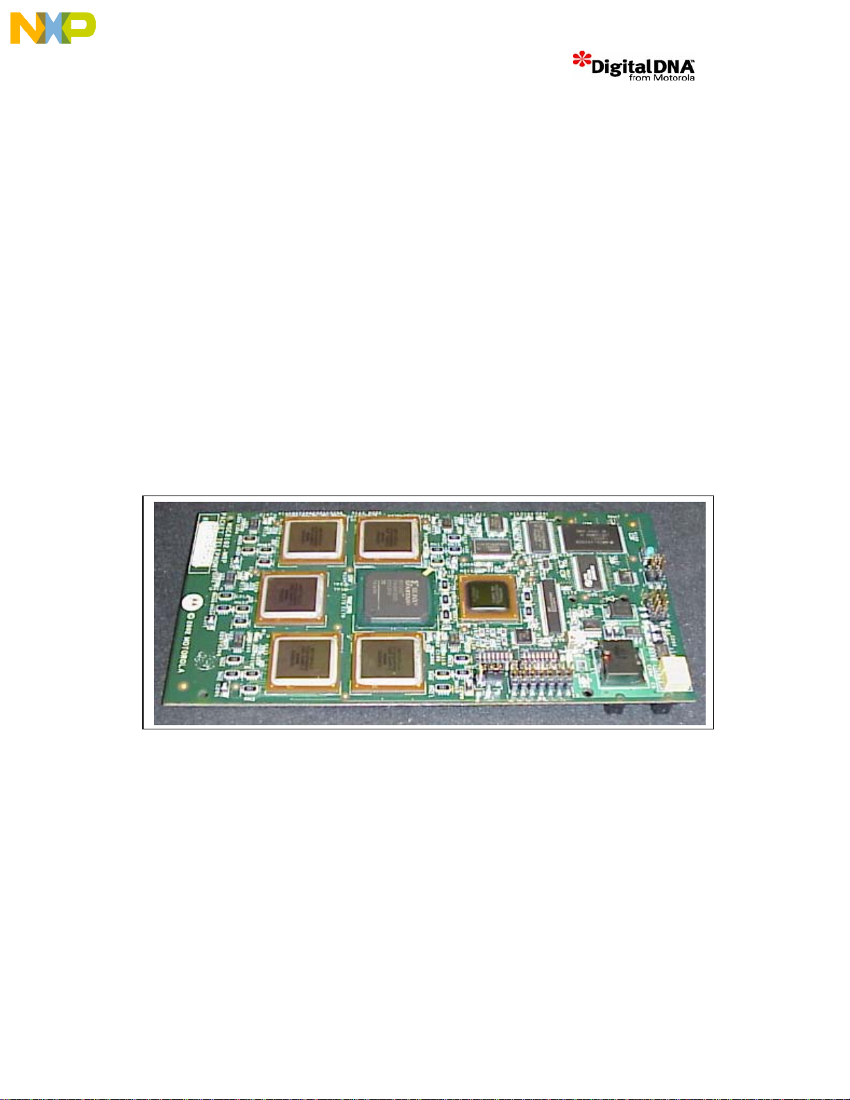
The Packet Telephony Farm Card is a PCI Telephony Mezzanine Card (PTMC) designed primarily as
an MSC8102 upgrade and Media Gateway evaluation product for Media Gateway Systems. It is
designed around the Star-Core MSC8102 16 bit fixed point DSP device from Motorola Semiconductor.
The PFC DSP farm card utilizes five MSC8102 devices and a MSC8101 to aggregate the data to/from
the DSP farm. Each MSC8102 DSP has an associated 4M x 32 (16MB) SDRAM. The aggregator has
a separate 2M x32 (8MB) SDRAM.
The PFC interfaces with a baseboard platform via its PTMC site. A PTMC is a PMC module, which
conforms to the PMC standard for Jn1 and Jn2, but uses Jn3 and Jn4 to support a variety of telecom
interfaces. The PTMC site on the Media Gateway is configured as PT3MC, a subset of the PTMC
specification, which supports UTOPIA, RMII and CT bus interfaces on Jn3/4. An optional fifth
connector (Jn5) has been added to support the two MII interfaces available from the MSC8101; Jn5 is
a proprietary connector, effectively supporting an enhanced PTMC, which is backward compatible
with existing PTMCs.
Data movement around the board is primarily through the use of 10/100 Mb/s Ethernet (single RMII or
dual MII interfaces) or UTOPIA and a Computer Telephony local bus through the PTMC connectors.
Additionally an I2C management interface is facilitated through PTMC J3 connect or. Additional I/O
includes HDI16, RS232 and OnCE JTAG ports for Debug.
The PFC is targeted to interface with Motorola Packet Telephony enhanced PTMC baseboards such as
the PDK demonstration system, as well as interfacing with standard customer PTMC Type III
baseboards.
Figure 1. MSC8102 - Packet Telephony Farm Card
2 PFC_DDD_v1.3.doc
Page 8

3 PFC Feature List
PFC Platfor m
Digital Support for up to 672 chan nels
PTMC Type 3 form card for interfacing to standard subsystems
MSC8101 Aggregator
One MSC8101 DSP communications processor with:
10/100BaseT Fast Ethernet via PTMC Interface
RMII Ethernet via PTMC Interface
UTOPIA interface via PTMC Interface
Host Interface to enable Host control of Aggregator via PTMC Interface
64-bit/32-bit PPC interface to the MSC8102 DSI port for on board data
distribution to DSP Farm
RS232 interface on board
4MByte of Flash for System Bootstrap
8MByte of SDRAM
MSC810 2 Farm
Five MSC8102s DSPs each with
TDM interface (CT Bus) via PTMC interface
64-bit/32-bit DSI Slave port interfacing to the MSC8101 PPC (via FPGA) for data
distribution
DSI-Asynchronous mode of ope ration
DSI-Synchronous mode of operation
16MByte of SDRAM
MSC8102 DSP1 has RS232 interface on board
FPGA
PPC to DSI translation for synchronous DSI
Transparent mode for asynchronous DSI
Routing of MSC8102 to MSC8101 interrupts
CPORT cluster interface
MII to RMII conversion
Debug
Chained DSP EONCE port with option to configure the full 5 MSC8102s and
MSC8101 chain or only the MSC8101 DSP.
SMC2 RS232 Connection to the MSC8101
UART connection to one MSC8102
Break out card allows access to Utopia interfaces via connectors
Power Supply
For stand al one ope rat i on 5V / 3.3V su ppl ie d e xte rn ally via bas e ca rd w it h opti on t o
supply 1.6V externally or via on board PFC 5V to 1.6V step down.
3 PFC_DDD_v1.3.doc
Page 9
4 User Guide
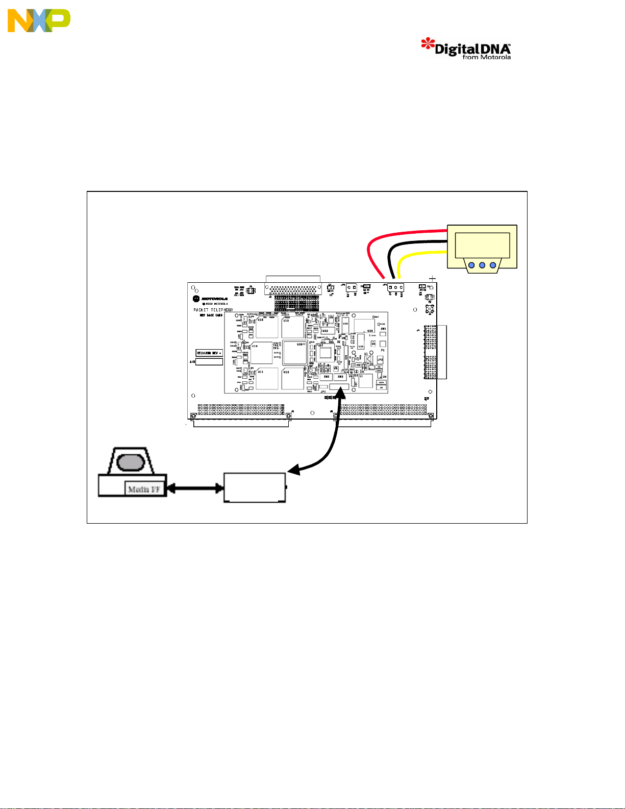
4.1 Quick Start
1. Start the Start the Codewarrior tools and ensure that the command converter is running
2. Connect a dual supply to the 5V, 3.3V and 0V on the JP1 connector of the Base Card.
3. The parallel command converter should also be connected to P 3 on the P FC to enable JTAG
access, reference Figure 2.
3.3V
0V
0V
3.3V
5V
5V
Host
Host
Host
Computer
Computer
Computer
Command
Command
Command
Converter
Converter
Converter
Figure 2. PFC Setup
4. Set the switch settings as per Table 2, Table 3 and Table 4.
5. Power up the PFC, which will now automatically bootstrap in the following modes:
• MSC8101 Boot from Flash
o Operating frequency: 275 MHz Core/ 138 MHz CPM / 69MHz system bus
• MSC8102 Boot through DSI
o Operating frequency: 250MHz core/ 83MHz system bus
o 32-bit asynchronous DSI
• JTAG of 21 cores
Each DSP LED will light after approximately 4 seconds (delay due to FPGA programming)
indicating a successful bootstrap.
6. The user can now use the StarCore Codewarrior tools to access the DSPs. Note that the user
should ensure the following:
o That reset on connect is NOT selected (a tools reset will restart the boot process,
preventing MSC8102 DSP JTAG access)
4 PFC_DDD_v1.3.doc
Page 10
o The JTAG file “PFCjtag21.cfg” is selected. The file listing and core JTAG
numbering is detailed in Appendix C.
Table 2. MSC8101 Boot from Flash
Feature Settings Comments
SW3.1 OFF
SW3.2 OFF
SW3.3 ON
SW3.4 ON Boot=0, Host Port disabled, Boot from external memory.
SW3.8 ON RSTCONF=0, Reset Configuration Master
Feature Settings Comm ents
SW2.1 OFF CNFGS=1 [MSC8102 Boot Over DSI]. Keeps MSC8102s in reset
SW2.2 ON
SW2.3 OFF
SW2.4 ON DSI64 =0, DSI is 32-bit
SW2.5 ON DSISYNC=0, DSI operates in asynchronous mode
SW2.6 ON SWTE=0, Software WDT disabled
SW2.7 ON RSTCONF=0 [MSC8102 Boot over DSI]. Keeps MSC8102s in reset
A_MODCK1 = 1
A_MODCK2= 1
A_MODCK3= 0
Table 3. MSC8102 Boot through DSI
until RCW received
MODCK2=0
MODCK1=1
until RCW received
MODCK 46 [101-110].
CLKIN=34.5MHz
Core/CPM/Bus= 275/138/69 MHz
MODCK 10 [010-10].
CLKIN=41.6MHz
Core/Bus= 250/83 MHz
SW3.6
SW3.7
OFF
ON
BM2: MSC8102 Boot Sequence through DSI
BM1
Table 4. Full chain (JTAG of 21)
Feature Settings Comments
JP1 Pos 1-2 Full Cha in
SW2.8 ON Full Chain
4.2 Board Configuration Options
4.2.1 Single MSC8101 with Default Configuration
To initialize the MSC8101 with its default Reset Configuration Word, set the switch settings detailed
in Table 5 and Table 8 (MSC8101 only). Note that this mode allow tools access to the MSC8101 only
(the MSC8102s will remain in reset), and should be used when the flash is blank or corrupted.
Table 5. MSC8101 Default Reset Configuration Word
Feature Settings Comments
SW3.1 OFF
SW3.2 OFF
SW3.3 ON
A_MODCK1 = 1
A_MODCK2= 1
A_MODCK3= 0
MODCK 6 [000-110].
CLKIN=34.5MHz
Core/CPM/Bus= 138/69/34.5 MHz
5 PFC_DDD_v1.3.doc
Page 11
SW3.4 ON Boot=0, Host Port disabled, Boot from external memory
SW3.8 OFF RSTCONF=1, Reset Configuration Slave
4.2.2 MSC8101 Boot through HDI16
To bootstrap the PFC through the MSC8101 HDI16 interface, set the switch settings detailed in Table
6 and Table 3.
Table 6. MSC8101 HDI16 Boot
Feature Settings Comments
SW3.1 OFF
SW3.2 OFF
SW3.3 ON
SW3.4 OFF Boot=1, Host Port enabled, MSC8101 boot from HDI16
SW3.8 OFF RSTCONF=1, Reset Configuration Slave
A_MODCK1 = 1
A_MODCK2= 1
A_MODCK3= 0
4.2.3 MSC8101 Ethernet/Utopia Options
Switch SW3.5 can be used to select the required MSC8101 CPM options as detailed below
Table 7. MSC8101 Ethernet/Utopia Options
Feature Settings Comments
SW3.5 ON FCC1
UTOPIA
SW3.5 OFF FCC1
Ethernet MII1
MODCK 46 [101-110].
CLKIN=34.5MHz
Core/CPM/Bus= 275/138/69 MHz
FCC2
Ethernet (MII2)
FCC2
Ethernet (MII2)
4.2.4 MSC8102 DSI Options
The MSC8102 DSI port cam be configured into 1 of 4 modes
• 32-bit wide Asynchronous Mode
• 64-bit wide Asynchronous Mode
• 32-bit wide Synchronous Mode
• 64-bit wide Synchronous Mode
The PFC is delivered with 32-bit wide asynchronous mode as standard, which is preprogrammed in
Flash memory. To implement a different mode the user should contact Motorola to obtain the required
firmware.
4.2.5 JTAG options
There are 2 JTAG options available as detailed in Table 8:
Table 8. JTAG Options
Description Feature Settings
MSC8101 only JP1 P os 2-3
6 PFC_DDD_v1.3.doc
Page 12

SW2.8 OFF
JP1 Pos 1-2 Full Chain (21 cores)
The JTAG configuration file for 21 cores is listed in Appendix C.
4.3 Programming Flash
The PFC uses the same Flash (AM29LV320DB) as the MSC8102ADS so the option exists to use
either the Metrowerks Code-warrior or PFC specific Flash Programmer (consult Motorola for
additi onal details on program ming Flash).
SW2.8 ON
7 PFC_DDD_v1.3.doc
Page 13
5 Hardware Description
This section describes the Packet Telephony Farm Card Hardware. The Hardware architecture has
been partitioned into the following logical sections: Aggregator, DSP Processing Array, General Board
Config ur at i o n, Fi r mware and P FC Ba s e Ca rd.
5.1 Board Architecture
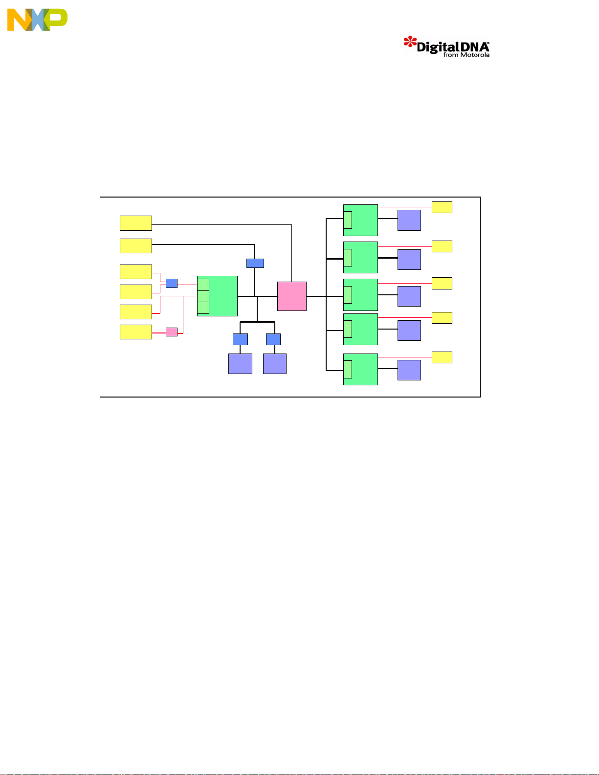
The board architecture of the Packet Telephony Farm Card is shown in Figure 3.
CT Bus
CT Bus
PN2
CT Bus
CT Bus
CT Bus
CT Bus
CT Bus
CT Bus
CT Bus
CT Bus
PN2
PN2
PN2
PN2
PN2
PN2
PN2
PN2
PN2
PN1
PN1
PN2
PN2
PN4
PN4
PN5
PN5
PN5
PN5
PN3
PN3
CPORT GMII
CPORT GMII
Interface
Interface
Host
Host
UTOPIA
UTOPIA
Ethernet
Ethernet
(MII 1)
(MII 1)
Ethernet
Ethernet
(MII 2)
(MII 2)
Ethernet
Ethernet
(RMII)
(RMII)
MUX
MUX
FPGA
FPGA
FCC1
FCC1
FCC2
FCC2
SMC2
SMC2
MSC8101
MSC8101
LATCH
LATCH
MUX
MUX
8MB
8MB
SDRAM
SDRAM
Buffer
Buffer
64/32-bit
64/32-bit
60x
60x
LATCH
LATCH
FLASH
FLASH
4MB
4MB
FPGA
FPGA
8-bit32-bit
8-bit32-bit
32/64-bit
32/64-bit
DSI
DSI
DSI
DSI
DSI
DSI
DSI
DSI
DSI
DSI
DSI
DSI
DSI
DSI
DSI
DSI
DSI
MSC8102
MSC8102
MSC8102
MSC8102
MSC8102
MSC8102
MSC8102
MSC8102
MSC8102
MSC8102
MSC8102
MSC8102
MSC8102
MSC8102
MSC8102
32-bit
32-bit
32-bit
32-bit
32-bit
32-bit
32-bit
32-bit
32-bit
32-bit
16MB
16MB
SDRAM
SDRAM
16MB
16MB
SDRAM
SDRAM
16MB
16MB
SDRAM
SDRAM
16MB
16MB
SDRAM
SDRAM
16MB
16MB
SDRAM
SDRAM
Figure 3. Packet Telephony Farm Card Architecture
This can be split into 2 main blocks
1. MSC8101 Aggregator Processor
2. MSC8102 Farm
Under typical operating conditions the MSC8101 is used to terminate ATM or 10/100BaseT Ethernet
packet traffic from a host card via its PTMC interface, with the subsequent data placed in the
MSC8101’s internal SRAM or external SDRAM. The data is then distributed to the MSC8102 farm for
processing via the MSC8102 DSI port with the FPGA performing the 60x bus to DSI translation
(NOTE: the FPGA has been incorporated to allow synchronous DSI transfer – it is not required for
asynchronous DSI transfers). After MSC8102 processing the data is dispatched through the MSC8102
TDM interfaces to the PTMC CT Bus.
5.2 MSC8101 Aggregator & 60x Bus Interface
The Aggregator terminates the packet protocol and transfers Media Data to and from the DSP Array
through its 60x bus. The 60x interface to the MSC8102 DSI can be configured as 32 or 64-bit wide.
When configured for 32-bit operation an external host can access the host port (HDI16) of the
MSC8101 aggregator for bootstrap and ongoing data exchange and control. 4 MB of 8-bit wide Flash
is connected to the MSC8101 60x bus for configuration, boot and execution code (for all 6 DSPs). 8
MBytes of 32-bit wide SDRAM also hangs off this bus to provide adequate storage during real time
operation. It should be noted that the address bus is latched to the SDRAM and Flash memories due to
the 60x compatible mode used (when running in DSI Synchronous mode). The data bus is un-buffered
to the memories and FPGA but buffered for the HDI16 port. The SDRAM is not required for normal
Aggregation functions and has been incorporated purely for maximum flexibility.
Table 9 details the MSC8101 Chip selects used for the 60x bus devices.
8 PFC_DDD_v1.3.doc
Page 14
Table 9. MSC8101 Memory Controller Resources
Chip Select
CS0 Flash (Boot)
CS2
CS3 DSI Asynchronous (Individual Chip Selects)
CS4 DSI Asynchronous (Broadcast mode)
SDRAM
5.2.1 MSC8101 SDRAM Interface
The Aggregator 60x bus incorporates 64M-bit x32-bit wide x4 bank Micron MT48LC2M32B2
SDRAM surface mounted onto the board providing 8 MBytes of general-purpose system RAM. The
MSC8101’s Chip Select 2 is used to select the SDRAM devices through the SDRAM controller, which
is capable of interfacing to JEDEC compatible SDRAM, the settings of which are now described.
• SDRAM size is 512k x 32 x 4 Ba nks = 8MBytes, which requires 2 3 a ddress lines.
• Device has 8 column and 11 Row lines, 2 Bank Selects. The 32-bit port size means addresses
30 and 31 are not used.
For Page based Interleaving the 60x bus is arranged as follows:
A[9:19] A[20:21] A[22:29] A[30:31]
Row (x11) Bank Select Column (x8) LSB
This gives the following MSC8101 Registers settings:
• PSDMR[PBI] = 1, Page Based Interleaving
• ORx[BPD] = 01, 4 Ba nks per device
• ORx[ROWST] = 1001, Row Starts at A9
• ORx[NUMR]= 010, SDRAM has 11 Row lines
From the SDRAM perspective during an ACTIVATE command it’s address port will look like:
A9:A19 A17:A18 A19:A29 A30:A31
--- Internal Bank Select
(A[20:21])
Peripheral
Row(A[9:19]) LSB
While a Read/Write will look like:
A9:A19 A17:A18 A[19:21] A[22:29] A30:A31
--- Internal Bank Select
(A[20:21])
Which gives the following regist er settings:
• PSDMR[SDAM] = 010, A[9:19] muxed to A[19:29]
• PSMDR[BSMA] = 100, A[17-18] are used as Bank Selects Signals
• PSMDR[SDA10] = 001, A9 maps to A10/AP pin
The full PSDMR settings are described in table
Table 10. MSC8101 PSDMR settings
Register Setting Description
PBI = 1 Paged Based Interleaving
RFEN = 1 Refresh services required
9 PFC_DDD_v1.3.doc
Don’t
care
Column
(A[22:29])
LSB
Page 15
OP = 000 Normal Operation
SDAM = 010 A[9:19] multiplexed to A[19:29]
BSMA = 100 A17-A18 are used as Bank Selects Signals
SDA10 = 001 A9 maps to A10/AP pin
RFRC = 110 8 Clock Cycles Refresh Recovery
PRETOACT = 011 Pre-charge to Activate 3 cycle interval
ACTTORW= 011 Activate to Read/Write 3 clock cycles
BL 23 = 1 Burst Length is 8
LDOTOPRE = 10 Precharge can be set 2 cycles before last data is read from SDRAM
WRC = 00 Precharge is set 4 cycles after the last data is written to SDRAM
EAMUX= 1 External Address Multiplexing, Fastest timing (set to 0 for MSC8102
SDRAM)
BUFCMD = 0 Normal Timing for the control lines
CL = 10 Cycle CA S Lat e ncy=2
These SDRAM settings are conservative and can be optimized for future configurations.
The OR & BR settings are described below:
Register Setting Description
BA=0x2000_0 Base Addre ss = 0x20000000
PS=11 32-bit port size
MSEL =010 SDRAM machine
Register Setting Description
SDAM = 1111 1111
1000
LSDAM = 0000 0 8MB SDRAM
BPD= 01 4 Banks Per Device
ROWST = 1001 R ow Star ts at A9
NUMR = 010 SDRAM has 11 Row lines
PMSEL = 0 Back to Back Page Mode (Normal Operation)
PSDMR = 0xC287378A: MSC8101 SDRAM
Table 11. MSC8101 BR & OR settings
0x20001841
IBID = 1 Bank Interleaving Disabled
After Power On a JEDEC standard initialization sequence is performed to configure the SDRAM. This
is carried out in Software utilizing the SDRAM controller PSDMR register:
OR = 0xFF803290
5.2.1.1 SDRAM Initialization Command Sequence
Step 1. Apply power and start clock. Maintain No Operation (NOP) condition at the inputs.
Step 2. Maintain stable power, stable clock and NOP input conditions at the inputs.
10 PFC_DDD_v1.3.doc
Page 16
Step 3. Issue Precharge All command (PALL) to all banks of the device. Program PSDMR[OP] bits to
[101] and then perform an access to the SDRAM bank.
Step 4. Issue 8 or more CBR Refresh (REF) commands. Program PSDMR[OP] bits to [001] and then
perform 8 accesses to the SDRAM bank.
Step 5. Issue Mode Register Set (MRS) command to initialise the mode register. Program
PSDMR[OP] bits to [011] and then performing an access to the SDRAM bank at an address offset to
0x08Csee figure below.
BL = Burst Length 8 for 32 Bit b us.
BT = 0 Sequential B ur s t s
CAS Latency = 2
OP MODE = Standard Operation
WB = 0 Programmed Burst Length
A10/
A9 A8 A7 A6 A5 A4 A3 A2 A1 A0
AP
SDRAM
Address
Lines
RSVD Burst Length
0 0 0 0 1 0 0 0 1 1
0
BTCAS LatencyWB Op Mode
MSC8101
Address
Lines
A19 A20 A21 A22 A23 A24 A25 A26 A27 A28 A29 A30 A31
0 0 0 0 1 0 0 0 1 10 0 0
SDRAM Only sees this part of the Bus
NC
Figure 4. MSC8101 SDRAM Mode Reg ister Settings
5.2.1.2 SDRAM Refresh
The SDRAM requires 4096 refresh cycles per 64ms or one refresh cycle per 15.625µs. The MSC8101
can be programmed to carry out the refresh cycle periodically using the SDRAM Refresh Timer
(PSRT). By setting the memory refresh timer prescaler register, MPTPR[PTP] to divide by 32, and the
PSRT to 0x30 a timer period of 15.625µs is realized for a 100MHz system clock . For a 69MHz
System clock PSRT = 0x17.
odxTimerPeriFPSRT
1625.15
usx
−=
PSRT
PSRT
=
MPTC
69
MHz
32
200
xPSRT
=
=
MPTC
100
MHz
32
300
=
xPSRT
odxTimerPeriFPSRT
1625.15
−=
usx
Figure 5. Refresh Calculations
5.2.2 MSC8101 FLASH Interface
The Aggregator incorporates an AM29LV320DB-120E 4Mx8-bit FLASH for Stand-alone reset
configuration and boot. To enable bootstrapping from reset the Flash is mapped to GPCM CS0 and
utilizes the following signals
Table 12. MSC8102 DSI Ad dresses
MSC8102 GPCM Signal
A_CS_FLASH CS0
A_PSDRAS POE
A_PSDDQMO WE
A_BADDR[27:30] A[3:0]
11 PFC_DDD_v1.3.doc
Page 17

A_BADDR[31] A-1
On the flash the BYTE signal is pulled down for byte mode which enables DQ[0:7] but tri-states
DQ[8:14], with D DQ15/A-1 used as an input for the LSB address bit, A _BADDR31. The memory
controller uses the BADDR[27-31] signals to interface to the memories when operating in multimaster mo de.
5.2.3 MSC8101 60x to DSI Interface
The 60x-DSI interface is the main means of communications between the Aggregator and the DSP
Farm. The DSI interface is configurable, and can be set to either 32 or 64bit wide, as well as
synchronous or asynchronous modes
• Asynchronous Mode: SRAM-like interface enabling the host single accesses (with no external
clock). Data is transfer red usi ng the MSC8101 Memory Co ntrolle r’s UPM.
• Synchronous Mode: SSRAM-like interface enabling host single or burst accesses of 256 bits
(8 accesses of 32 bits or 4 accesses of 64 bits) with its external clock decoupled from the
MSC8102 internal bus clock. Data transferred in this mode is passed onto the external 60x
bus to be handled by the FPGA
The DSI gives external hosts direct access to the MSC8102 internal memory space, including on-chip
memories and the registers of the on-chip modules. The DSI write buffer stores the address and the
data of the accesses until they are performed. The external host can therefore perform multiple writes
without waiting for those accesses to complete. Latencies that are typical during accesses to on-chip
memories are greatly reduced by the DSI read prefetch mechanism. The host addresses each of the
MSC8102 devices using a single chip-select with the most significant bits on the address bus
identifying the addressed MSC8102 device. The 4-bit MSC8102 DSI address is hardwired via
CHIP_ID [0:3], Table 13
Table 13. MSC8102 DSI Ad dresses
MSC8102 CHIP_ID[0:3]
1 0000
2 0001
3 0010
4 0011
5 0100
The host can also write the same data to multiple MSC8102 devices simultaneously by asserting a
dedica ted broad cast chi p s elect.
5.2.3.1 MSC8101 60x to DSI Interface: Synchronous mode
In synchronous mode an FPGA is required to interface between the MSC8101 60x bus and the
MSC8102 DSI port. The connectivity is detailed in Figure 6.
12 PFC_DDD_v1.3.doc
Page 18

Dh[0:63]
Dh[0:63]
Ah[0:31]
Ah[0:31]
A_TSIZ[0:3]
A_TSIZ[0:3]
A_PUPMWAIT
A_PUPMWAIT
A_TS
A_TS
A_TBST
MSC8101
MSC8101
Note: All unused PPC
Note: All unused PPC
signals on host side pulled
signals on host side pulled
high
high
A_TBST
A_PSDVAL
A_PSDVAL
A_TT[0:4]
A_TT[0:4]
A_BADDR[27:31]
A_BADDR[27:31]
A_AACK
A_AACK
A_TA
A_TA
A_ALE
A_ALE
A_PSDQM[0:7]
A_PSDQM[0:7]
A_BCTL[0:1]
A_BCTL[0:1]
A_CS_HCS
A_CS_HCS
A_CS_HBCS
A_CS_HBCS
PGPL2
PGPL2
A_CLK_OUT
A_CLK_OUT
FPGA_CK
FPGA_CK
HCK_D[1:5]
HCK_D[1:5]
ICS9112
ICS9112
(Zero delay buffer)
(Zero delay buffer)
GRP_Ds[0:63]
GRP_Ds[0:63]
GRP_Ah[7:29]
GRP_Ah[7:29]
FPG
FPGA
Xilinix XC2S300E - 7F - G456C
Xilinix XC2S300E - 7F - G456C
Figure 6. PFC to DSI Interface
HBRST
HBRST
HTA
HTA
HWBS[0:7]
HWBS[0:7]
HRW
HRW
HCS
HCS
HBCS
HBCS
MSC8102 – CHIP_ID[0:3]
MSC8102 – CHIP_ID[0:3]
--------------------------
-------------------------DSP1 0000
DSP1 0000
DSP2 0001
DSP2 0001
DSP3 0010
DSP3 0010
DSP4 0011
DSP4 0011
DSP5 0100
DSP5 0100
GRP_Ah[11:29]
GRP_Ah[11:29]
GRP_Ah[7:10]
GRP_Ah[7:10]
HCK_D1
HCK_D1
HCK_D2
HCK_D2
HCK_D3
HCK_D3
HCK_D4
HCK_D4
HCK_D5
HCK_D5
3V3
3V3
HD[0:63]
HD[0:63]
HA[11:29]
HA[11:29]
HCID[0:3]
HCID[0:3]
MSC8102
MSC8102
[x5]
[x5]
HDST[0:1]
HDST[0:1]
CHIP_ID[0:3]
CHIP_ID[0:3]
HCLKIN
HCLKIN
5.2.3.2 MSC8101 60x to DSI Interface: Asynchronous mode
The DSI can be asynchronously controlled via the following UPM signals:
Table 14. DSI Asynchronous signals
UPM Signal Description
CS3 Broadcast Chip Select
CS4 Chip Select
PBS[0:7] Byte Strobe
PGPL2 General Purpose
PGPL4/UPMWAIT UPMWAIT
These signals are routed through the FPGA, which operates in transparent mode.
5.2.4 MSC8101 to MSC8102 Interrupt Connectivity
The FPGA is used to route the interrupts/GPIO lines between the MSC8101 and MSC8102s. For
flexibility the MSC8101 has 5 GPIO lines (PC4, PC5, PC24, PC25 & PC30) connected to the FPGA
and in turn receives 7 IRQ inputs from the FPGA. Each MSC8102 has GPIO30 and INT_OUT
connected to the FPGA, with their respective IRQ1 and IRQ2 also connected, Figure 7. The standard
pre-programmed FPGA interrupt routing is shown in Figure 8.
13 PFC_DDD_v1.3.doc
Page 19

IRQ1_D1
MSC
8101
A_IRQ[1:7]
DSP_IRQ_GPIO[1:5]
FPGA
IRQ2_D1
GPIO30_D1
INT_OUT_D1
IRQ1_D2
IRQ2_D2
GPIO30_D2
INT_OUT_D2
IRQ1_D3
IRQ2_D3
GPIO30_D3
INT_OUT_D3
IRQ1_D4
IRQ2_D4
GPIO30_D4
INT_OUT_D4
IRQ1_D5
IRQ2_D5
GPIO30_D5
INT_OUT_D5
MSC8102
#1
MSC8102
#2
MSC8102
#3
MSC8102
#4
MSC8102
#5
Figure 7. Aggregator MSC8102 Interrupt Connectivity Options
MSC 8101
FPGA
A_IR Q1
DSP_IRQ_ GP IO1 (P C4 )
A_IR Q4
DSP_IRQ_ GP IO2 (P C5 )
A_IR Q5
DSP_IRQ_GPIO3 (PC24)
A_IR Q6
DSP_IRQ_GPIO4 (PC25 )
A_IR Q7
DSP_IRQ_GPIO5 (PC30 )
INT_OUT_D1
GPIO30_D1
INT_OUT_D2
GPIO30_D2
INT_OUT_D3
GPIO30_D3
INT_OUT_D4
GPIO30_D4
INT_OUT_D5
GPIO30_D5
MSC8102
#1
MSC8102
#2
MSC8102
#3
MSC8102
#4
MSC8102
#5
Figure 8. Standard Interrupt Routing
14 PFC_DDD_v1.3.doc
Page 20

5.2.5 MSC8101 FCC Interface
The MSC8101 incorporates two FCC interfaces for packet transfers. The packet interfaces are
configur a bl e t o pe rf or m 2 xM II port s (F CC1 & FCC 2) or an M II ( FC C1 ) pl us a U TOP I A (FC C2) por t.
Both configurations are routed out to the PTMC connector as detailed in Table 15. Signals that are
common between UTOPIA FCC1 and MII FCC1 are routed to their connector positions via a
PERICOM P13B16233 bus switch.
Table 15. FCC1 Interface
PIN Function Signal Connects to
PA10 FCC1 Utopia II RxD0 Pn4-60
PA11 FCC1 Utopia II RxD1 Pn4-58
PA12 FCC1 Utopia II RxD2 Pn4-54
PA13 FCC1 Utopia II RxD3 Pn4-52
PA14 FCC1 Utopia II Rx4 / MII1 RxD3 Pn4-48 / Pn5-54
PA15 FCC1 Utopia II Rx5 / MII1 RxD2 Pn4-46 / Pn5-50
PA16 FCC1 Utopia II Rx6 / MII1 RxD1 Pn4-42 / Pn5-48
PA17 FCC1 Utopia II Rx7 / MII1 RxD0 Pn4-40 / Pn5-46
PA18 FCC1 Utopia II Tx7 / MII1 TxD0 Pn4-35 / Pn5-41
PA19 FCC1 Utopia II Tx6 / MII1 TxD1 Pn4-37 / Pn5-43
PA20 FCC1 Utopia II Tx5 / MII1 TxD2 Pn4-47 / Pn5-45
PA21 FCC1 Utopia II Tx4 / MII1 TxD3 Pn4-49 / Pn5-47
PA22 FCC1 Utopia II Tx3 Pn4-53
PA23 FCC1 Utopia II Tx2 Pn4-55
PA24 FCC1 Utopia II Tx1 Pn4-59
PA25 FCC1 Utopia II Tx0 Pn4-61
PA26 FCC1 Utopia II RxCLAV / MII1 RX_ER Pn4-18 / Pn5-56
PA27 FCC1 Utopia II RxSOC / MII1 RX_DV Pn4-49 / Pn5-64
PA28 FCC1 Utopia II RXENB/ MII1 TX_EN Pn4-16 / Pn5-53
PA29 FCC1 Utopia II TXSOC/ MII1 TX_ER Pn4-1 / Pn5-55
PA30 FCC1 Utopia II TXCLAV / MII1 CRS Pn4-5 / Pn5-58
PA31 FCC1 Utopia II TXENB / MII1 COL Pn4-49 / Pn5-22
PC6 FCC1 Utopia II RXADDR2 Pn4-24
PC7 FCC1 Utopia II TXADDR2 Pn4-19
PC12 FCC 1 Utopia II RXADDR1 Pn4-30
PC13 FCC1 Utopia II TXADDR Pn4-28
PC14 FCC 1 Utopia II RXADDR0 Pn4-34
PC15 FCC1 Utopia II TXADDR0 Pn4-29
PC30 FCC1 Utopia II TXCLK / MII1 TCLK Pn4-25 / Pn5-64
PC31 FCC1 Utopia II RXCLK / MII1 RCLK Pn4-43 / Pn5-60
PD7 FCC1 Utopia II TXADDR3 Pn4-17
15 PFC_DDD_v1.3.doc
Page 21

PD16 FCC1 Utopia II TXPRTY Pn4-31
PD17 FCC1 Utopia II RXPRTY Pn4-36
PD18 FCC1 Utopia II RXADDR4 Pn4-4
PD19 FCC1 Utopia II TXADDR4 Pn4-6
PD29 FCC1 Utopia II RXADDR3 Pn4-7
Table 16. MSC8101 Aggregator FCC2 PTMC Connectivity
PIN Function Signal Connects to
PB18 FCC2 MII2 RXD3 Pn5-34
PB19 FCC2 MII2 RXD2 Pn5-30
PB20 FCC2 MII2 RXD1 Pn5-28
PB21 FCC2 MII2 RXD0 Pn5-26
PB22 FCC2 MII2 TXD0 Pn5-21
PB23 FCC2 MII2 TXD1 Pn5-23
PB24 FCC2 MII2 TXD2 Pn5-25
PB25 FCC2 MII2 TXD3 Pn5-27
PB26 FCC2 MII2 CRS Pn5-38
PB27 FCC2 MII2 COL Pn5-37
PB28 FCC2 MII2 RX_ER Pn5-36
PB29 FCC2 MII2 TX_EN Pn5-33
PB30 FCC2 MII2 RX_DV Pn5-24
PB31 FCC2 MII2 TX_ER Pn5-35
5.2.6 RMII Interface
The MSC8101 FCC2 signals are routed to the FPGA to allow conversion of FCC2’s MII interface to
RMII enabling connection to the PTMC Type III RMII port on connector PN3.
5.2.7 MSC8101 I2C Controller
An I2C Management for customer specific application.is incorporated on the MSC8101 via J14 Pin 57
[SDA] and J1 4 Pi n 9 [ SC L] . Th e o pti on (vi a 0 oh m re si st or s) t o pr ovi de a st an dar d P TM C I2C is a ls o
provided for on Jn1 Pin 41 [SCL] and Pin 42 [SDA].
5.2.8 MSC8101 RS232 Interface
A simple RS232 UART is provided through the MSC8101’s Serial Management Channel interface
(SMC2) t o gi ve program ma ble debu g or co m m un ic a t io n s c a pa bi l ity. A Max im M AX 3241 pr ovides the
level conversion for the interface.
5.2.9 MSC8101 Host Interface (HDI16)
The 16-bit Host port on the MSC8101 can be used for bootstrapping and ongoing data and control flow
from a Host processor if desired. The port connects to PTMC connector PN2 via an IDTQ34XV245Q3
bus switch controllable by the host signal PTENB, by default the switch is open whish isolates any
host data signals.
A host processor accessing the MSC8101 aggregator should do so in the following mode
16 PFC_DDD_v1.3.doc
Page 22

Table 17. HDI6 Conf igur ation
60x signal HDI16 Signal Description
Dh57 HDSP=0 Sing le data strobe mode
Dh58 HDDS=0 Negative data strobe polarity
Dh59 H8BIT=0 16-bit mode enabled
Dh60 HCS2=1 Not used, pulled high
Note that when using the host port the DSI interface must be configured for 32-bits
5.3 MSC8102 DSP Processing Array
The DSP farm contains 5 MSC8102 DSPs connected to the MSC8101 via a shared DSI 60x bus
interface. Each DSP has access to 16MB of SDRAM. The DSPs interface to the PSTN world through
the PTMC connector via their TDM links. In addition MSC8102 DSP1 (U19) has an SMC U ART
connection to an onboard connector.
5.3.1 DSP Array SDRAM Configuration
Each DSP incorporates 128M-bit x32-bit wide x4 bank Micron MT48LC4M32B2 SDRAM surface
mounted onto the board providing 16 MBytes of general-purpose system RAM. The MSC8102’s Chip
Select 2 is used to select the SDRAM devices through the SDRAM controller, which is capable of
interfacing to JEDEC compatible SDRAM, the settings of which are now described.
• SDRAM size is 1M x 32 x 4 Banks = 16MBytes, which requires 24 address lines.
• Device has 8 column and 12 Row lines, 2 Bank Selects. The 32-bit port size means addresse s
30 and 31 are not used.
For Page based interleaving the 60x bus is arranged as follows:
A[8:19] A[20:21] A[22:29] A[30:31]
Row (x12) Bank Select Column (x8) LSB
This gives the following MSC8101 Registers settings:
• PSDMR[PBI] = 1, Page Based Interleaving
• ORx[BPD] = 01, 4 Ba nks per device
• ORx[ROWST] = 1000, Row Starts at A8
• ORx[NUMR]= 011, SDRAM has 12 Row lines
From the SDRAM perspective during an ACTIVATE command it’s address port will look like:
A9:A19 A16:A17 A18:A29 A30:A31
--- Internal Bank Select
(A[20:21])
Row(A[8:19]) LSB
While a Read/Write will look like:
A9:A19 A16:A17 A[18:21] A[22:29] A30:A31
--- Internal Bank Select
(A[20:21])
This gives the following register settings:
• PSDMR[SDAM] = 010, A[9:19] multiplexed to A[19:29]
• PSMDR[BSMA] = 011, A[16-17] are used as Bank Selects Signals
• PSMDR[SDA10] = 001, A9 maps to A10/AP pin
The full PSDMR settings are described in table
17 PFC_DDD_v1.3.doc
Don’t
care
Column
(A[22:29])
LSB
Page 23

Table 18. MSC8102 PSDMR settings
Register Setting Description
PBI = 1 Paged Based Interleaving
RFEN = 1 Refresh services required
OP = 000 Normal Operation
SDAM = 010 A[9:19] muxed to A[19:29]
BSMA = 011 A16-A17 are used as Bank Selects Signals
SDA10 = 001 A9 maps to A10/AP pin
RFRC = 110 8 Clock Cycles Refresh Recovery
PRETOACT = 011 Pre-charge to Activate 3 cycle interval
ACTTORW= 011 Activate to Read/Write 3 clock cycles
BL 23 = 1 Burst Length is 8
LDOTOPRE = 10 Precharge can be set 2 cycles before last data is read from SDRAM
WRC = 00 Precharge is set 4 cycles after the last data is written to SDRAM
EAMUX= 1 SDAMUX asserted for an extra cycle
BUFCMD = 0 Normal Timing for the control lines
CL = 10 Cycle CA S Lat e ncy=2
These SDRAM settings are conservative and can be optimized for future configurations.
The OR settings are described below:
BR Register Setting Description
BA=0x2000_0 Base Addre ss = 0x20000000
PS=11 32-bit port size
MSEL =010 SDRAM machine
OR Register Setting Description
SDAM = 1111 1111
0000
LSDAM = 0000 0 16MB SDRAM
BPD= 01 4 Banks Per Device
ROWST = 1000 R ow Star ts at A8
NUMR = 010 SDRAM has 12 Row lines
PSDMR = 0xC267378A: MSC8102 SDR AM
Table 19. MSC8102 BR & OR Settings
BR = 0x20001841
PMSEL = 0 Back to Back Page Mode (Normal Operation)
IBID = 1 Bank Interleaving Disabled
After Power On a JEDEC standard initialization sequence is performed to configure the SDRAM. This
is carried out in Software utilizing the SDRAM controller PSDMR register:
18 PFC_DDD_v1.3.doc
OR = 0xFF003090
Page 24

27
0
x
PSRT
5.3.1.1 SDRAM Initialization Command Sequence
Step 1. Apply power and start clock. Maintain No Operation (NOP) condition at the inputs.
Step 2. Maintain stable power, stable clock and NOP input conditions at the inputs.
Step 3. Issue Precharge All command (PALL) to all banks of the device. Program PSDMR[OP] bits to
[101] and then perform an access to the SDRAM bank.
Step 4. Issue 8 or more CBR Refresh (REF) commands. Program PSDMR[OP] bits to [001] and then
perform 8 accesses to the SDRAM bank.
Step 5. Issue Mode Register Set (MRS) command to initialise the mode register. Program
PSDMR[OP] bits to [011] and then performing an access to the SDRAM bank at an address offset to
0x08Csee figure below.
BL = Burst Length 8 for 32 Bit b us.
BT = 0 Sequential B ur s t s
CAS Latency = 2
OP MODE = Standard Operation
WB = 0 Programmed Burst Length
A10/
A9 A8 A7 A6 A5 A4 A3 A2 A1 A0
AP
SDRAM
Address
Lines
RSVD Burst Length
0 0 0 0 1 0 0 0 1 1
0
BTCAS LatencyWB Op Mode
MSC8101
Address
Lines
A19 A20 A21 A22 A23 A24 A25 A26 A27 A28 A29 A30 A31
0 0 0 0 1 0 0 0 1 10 0 0
SDRAM Only sees this part of the Bus
NC
Figure 9. SDRAM M ode Regis ter Settings
5.3.1.2 SDRAM Refresh
The SDRAM requires 4096 refresh cycles per 64ms or one refresh cycle per 15.625µs. The MSC8101
can be programmed to carry out the refresh cycle periodically using the SDRAM Refresh Timer
(PSRT). By setting the memory refresh timer prescaler register , MPTPR[PTP] to divide by 32, and the
PSRT to 0x30 a timer period of 15.625µs is realised for a 100MHz system clock . For a 83MHz
System clock PSRT = 0x17.
PSRT
PSRT
=
MPTC
83
MHz
32
=
=
MPTC
100
MHz
32
300
xPSRT
=
odxTimerPeriFPSRT
1625.15
usx
−=
odxTimerPeriFPSRT
−=
1625.15
usx
Figure 10. Refresh Calculations
5.3.2 MSC8102 Array DSI Interface
The MSC8102’s DSI interface is the main means of packet media transfers to and from the DSP Array.
The DSI is configurable between 32 and 64 bit modes of operation using Dip Switch SW2.
5.3.3 MSC8102 Array TDM Interface
The CT bus is split into 32 streams of 128 timeslots each, giving 4096 timeslots. Each MSC8102
TDM link is uni-directional, meaning two CT Streams are required to interf ace with the MSC8102
19 PFC_DDD_v1.3.doc
Page 25

TDM0TCLK
TDM0 T
DAT
MSC8102
TDM0TCLK
TDM0 T
DAT
TDM3 TDAT
MSC8102
TDM0TCLK
TDM0 T
DAT
MSC8102
CT_D0
CT_D12
TDM0TCLK
TD
M0T
DAT
MSC8102
TDM0TCLK
TDM0 T
DAT
MSC8102
CT_D14
TDM. With the P3TMC specification implemented the number of CT lines is further restricted to 20
streams.
Each MSC8102 has four TDM interfaces. The TDM Streams are routed as follows:
CT_C8_
CT_FRAME_
CT_C8_A_B
CT_FRAME_A_B
CT_C8_A_B
CT_FRAME_A_B
CT_C8_A_B
CT_FRAME_A_B
TDM0TSYN
TDM1TCLK
TDM1TSYN
TDM2TCLK
TDM2TSYN
TDM3TCLK
TDM3TSYN
TDM0TSYN
TDM1TCLK
TDM1TSYN
TDM2TCLK
TDM2TSYN
TDM3TCLK
TDM3TSYN
TDM0TSYN
TDM1TCLK
TDM1TSYN
TDM2TCLK
TDM2TSYN
TDM3TCLK
TDM3TSYN
TDM0TSYN
TDM1TCLK
TDM1TSYN
TDM2TCLK
TDM2TSYN
TDM3TCLK
TDM3TSYN
TDM0TSYN
TDM1TCLK
TDM1TSYN
TDM2TCLK
TDM2TSYN
TDM3TCLK
TDM3TSYN
TDM0RDAT
TDM1TDAT
TDM1RDAT
TDM2TDAT
TDM2RDAT
TDM3TDAT
TDM3RDAT
TDM0RDAT
TDM1 TDAT
TDM1RDAT
TDM2 TDAT
TDM2RDAT
TDM3 TDAT
TDM3RDAT
TDM0RDAT
TDM1 TDAT
TDM1RDAT
TDM2 TDAT
TDM2RDAT
TDM3 TDAT
TDM3RDAT
TDM0RDAT
TDM1 TDAT
TDM1RDAT
TDM2 TDAT
TDM2RDAT
TDM3RDAT
TDM0RDAT
TDM1 TDAT
TDM1RDAT
TDM2 TDAT
TDM2RDAT
TDM3 TDAT
TDM3RDAT
Figure 11. TDM to CT Rout ing
MSC8102 TDM Ref. MSC8 102 Signal CT Stream Signal
MSC8102 #1 TDM0 TDM0TDAT
TDM0RDAT
TDM1 TDM1TDAT
TDM1RDAT
TDM2 TDM2TDAT
TDM2RDAT
TDM3 TDM3TDAT
TDM3RDAT
MSC8102 #2 TDM0 TDM0TDAT
TDM0RDAT
TDM1 TDM1TDAT
TDM1RDAT
TDM2 TDM2TDAT
TDM2RDAT
TDM3 TDM3TDAT
TDM3RDAT
MSC8102 #3 TDM0 TDM0TDAT
TDM0RDAT
TDM1 TDM1TDAT
TDM1RDAT
CT_D0
CT_D1
CT_D2
CT_D3
CT_D4
CT_D5
CT_D6
CT_D7
CT_D0
CT_D1
CT_D2
CT_D3
CT_D4
CT_D5
CT_D6
CT_D7
CT_D12
CT_D13
CT_D18
CT_D19
CT_D1
CT_D2
CT_D3
CT_D4
CT_D5
CT_D6
CT_D7
CT_D13
CT_D18
CT_D19
CT_D15
CT_D10
CT_D11
CT_D16
CT_D17
CT_D8
CT_D9
20 PFC_DDD_v1.3.doc
Page 26

12
R
TDM2 TDM2TDAT
TDM2RDAT
TDM3 TDM3TDAT
TDM3RDAT
MSC8102 #4 TDM0 TDM0TDAT
TDM0RDAT
TDM1 TDM1TDAT
TDM1RDAT
TDM2 TDM2TDAT
TDM2RDAT
TDM3 TDM3TDAT
TDM3RDAT
MSC8102 #5 TDM0 TDM0TDAT
TDM0RDAT
TDM1 TDM1TDAT
TDM1RDAT
TDM2 TDM2TDAT
TDM2RDAT
TDM3 TDM3TDAT
TDM3RDAT
Table 20. TDM to CT Stream Ro uting
The MSC8102s are configured in their four-pin setup with common clock and frame syncs for receive
and transmit. The clock and Frame Sync signals routed from the PTMC CT Bus are CT_8_A and
CT_FRAME_A respectively.
CT_D12
CT_D13
CT_D18
CT_D19
CT_D14
CT_D15
CT_D10
CT_D11
CT_D16
CT_D17
CT_D8
CT_D9
CT_D14
CT_D15
CT_D10
CT_D11
CT_D16
CT_D17
CT_D8
CT_D9
5.3.4 MSC8102 RS232 Interface
A simple RS232 UART is provided through the MSC8102’s serial communications interface (SCI) to
give programmable debug or communications capability. A Maxim MAX3232CUE provides the level
conversion for the interface. Note that the receiver inputs are pulled low internally while the
transmitter inputs have external pull-ups.
5.4 General Board Configuration
5.4.1
Reset
Figure 12 illustrates the reset scheme. The MAXIM MAX6828 generates the primary reset for the PFC
(PORESET), which is supplied to the MSC8101, MSC8102s (AND with MSC8101 GPIO: PA7),
FPGA and Flash memory. The Open drain output (RESET_N) is pulled low (for a minimum time out
period of 140ms) when any of the f ollowin g conditions occur:
• MR_N is pulled low via the pushbutton switch SW1
• The 1V6 voltage monitor trip voltage is reached (1.23Von Reset In pin),
1210
RR
+
tripVmonitor
(63.0_
=
• The threshold voltage on 3V3 is reached (MIN = 2.85V, MAX = 3.00V, TYP = 2.93V)
)
21 PFC_DDD_v1.3.doc
Page 27

1V6
R10
R12
Reset In
MR
3V3
VCC
A_PORESET
RESET
PORESET_M1
PORESET_FPGA
Figure 12. PORESET Sc heme
The MSC8101 controls the generation of individually buffered HRESET signals to the MSC8102s
through the AND gating of its own HRESET signal and its HRESET GPIO control line PD31. Note
that for f lexibility the MSC8102 HRESETS have been routed to the FPGA via 0ohm resistors.
The PMCC signal PTMC_RESET can be used by a prospective PFC base card host to control the
HRESET of the PFC.
The SRESET signals for the MSC8101 and MSC8102s have all been pulled high.
PTMC Connector
Pn2 pin 13
FLASH
MSC8101
GPIO[PA7]
FPGA
A_PORESET_M1
MSC8102
MSC8102
MSC8102
MSC8102
MSC8102
PTMC_RESET
MSC8101
HRESET
PD31
A_HRESET
A_M_HRESET
HRESET signals
(pulled up)
MSC8102
MSC8102
MSC8102
MSC8102
MSC8102
Figure 13. HRESET Scheme
5.4.2 Cloc k Distribution
The PFC has two clock regions
1. MSC8101 Aggregator and MSC8102 DSI interface clocking, Figure 14
2. MSC8102 and associated SDRAM clocking, Figure 15
In the first clock region the MSC8101 Aggregator and MSC8102 DSI interface clocks (HCK) are
generated via a single oscillator, which is distributed via an ICS9112-17 low skew buffer.
In the second clock region the MSC8102 CLKIN signals are generated from a single oscillator, which
is distributed via the ICS9112-16 low skew output buffer to the MSC8102 farm. Each MSC8102
CLKOUT s i gn al is in turn fed ba c k as the D L LIN signal via an addit i on a l l ow s ke w bu f fe r . This buffer
also generates the MSC8102’s associated SDRAM clock
To accommodate debug and board set up the following clock frequencies are used on the MSC8101
and MSC8102.
Table 21. MSC8101 Clock frequencies
Clock Mode CLKIN Core CPM Bus
46 34.5 MHz 275 MHz 138 MHz 69 MHz
Table 22. MSC8102 Clock frequencies
Clock Mode CLKIN Core Bus DSI
10 41.6 MHz 250 MHz 83 MHz 69 MHz
22 PFC_DDD_v1.3.doc
Page 28

MSC8102
MSC8102
MSC8102
MSC8102
MSC8102
MSC8102
Oscillator.
MSC8102
MSC8102
MSC8102
MSC8102
The frequency of operation will depend on the revision of silicon used and the required application.
Consult Motorola Ltd for the latest operating frequency characteristics of the MSC8101 and
MSC8102.
Note that to ensure synchronous operation the following layout constraints are placed:
• The MSC8102 CLKIN_D[1:5] are of equal length
• The MSC8101 derived clocks: FPGA _CK, SDRAMCKA, A_DLLIN, HCK_D[1:5]
are of equal length.
• On the MSC8102s the signals D1_DLLINx, SDRMCKx are of equal length
FPGA_CK
FPGA
MSC8101
Oscillator
MSC8102
CLKIN
MSC8101
A_DLLIN
CLKOUT
Figure 14. MSC8101 Aggregator Clocking Sc heme
CLKIN_D1
#1
DLLIN
CLKIN_D2
#2
SDRAMCKA
HCK_D1
HCK_D2
HCK_D3
HCK_D4
HCK_D5
CLKOUT
SDRAMCK
SDRAM
#1
#2
#3
#4
#5
SDRAM
SDRAM
ICS9112-16
CLKIN_D3
CLKIN_D4
CLKIN_D5
#3
SDRAM
SDRAM
#4
SDRAM
#5
Figure 15. MSC8102 and SDRAM Clocking
23 PFC_DDD_v1.3.doc
Page 29

1
5
VR
R
Vout
5.4.3 Power
The PICMG 2.15 standard currently stipulates that 5V, 3.3V and GND are provided through the PTMC
connectors. The optional connector, Pn5/Jn5 has the capabilities to supply the core voltage, 1.6V to the
card. In this configuration, there is no need for additional regulation on the card. However, in order to
interface with standard PTMC cards Pn5/Jn5 may not be populated – therefore in this scenario the core
voltage cannot be obtained through the PTMC connectors. To compensate for this the PFC uses a
Maxim MAX1714 Buck Controller to step down from 5V (Supplied via Jn1/Pn1) to 1.6V, capable of
supplying 8A. A link is provided to isolate this 1V6 suppl y when required. Pulling the MAX1714 pin
SHDN low can also disable the 1V6. (a resistor pad is provided for this).
The 1V6 output voltage can be adjusted from 1.3V to 2.0V as per Figure 16. The equation for
adjusting the output voltage is:
4
1(
VfbVout
R
+=
)
: Vfb =1.0V, R4=R5=1K and VR=2K
+
R4
Vfb
R5
VR1
Figure 16. Setting Vout with Resistor-Divider
The FPGA requires 1V8 supply and a minimum 500mA (for a few millisecs) on power up. Note that
the operating power requirements of the FPGA are application specific. A Maxim MAX8869EU18
linear regulator, which can give a guaranteed 1A, is used to supply the 1V8.
5.4.4 FPG A Co nf i gu ra ti o n
The FPGA is configured with the following:
• M[0:2] = 110, Slave Serial Mode with pre-configuration pull ups
• CCLK: Input clock in slave mode
• PROGRAM_N: initiates a configuration sequence when low.
5.4.5 PT M C Conne c tor s
The PFC is designed to interface with the PTMC connectors implemented on a Media Gateway
Platform. The PFC implements an enhanced PTMC Type III or P3 TMC c onfi gura tion, in corp orati ng
an additional optional connector, Pn5 to allow the inclusion of 2x MII capabilities. In general the 5
connectors interface is:
• Pn1 - CPORT interface
• Pn2 - Host Port Interface
• Pn3 - CT Bus, Ethernet-RMII
• Pn4 - UTOPIA Interface
• Pn5 - Ethernet (MII1 & MII2)
The connector pin out uti lized is listed in Table 23 t o Table 27:
24 PFC_DDD_v1.3.doc
Page 30

Color Meaning
N ot C onnected
Ground
Voltage
C T (TDM) Bus
Host Interface Signals
General Data I/O
PIN SIGNAL SIGNAL PIN
1NC NC2
3 GND NC 4
5NC NC6
7NC +5V8
9NC NC10
11 GND NC 12
13 GMII_CK GND 14
15 GND NC 16
17 NC +5V 18
19 VIO NC 20
21 NC CP14_D0 22
23 CP13_D6 GND 24
25 GND CP14_D1 26
27 CP13_D5 CP14_D2 28
29 CP13_D4 +5V 30
31 CP13_D3 CP14_D3 32
33 CP13_D2 GND 34
35 GND CP14_D4 36
37 CP13_D1 +5V 38
39 GND CP14_D5 40
41 CP13_D0 CP14_D6 42
43 CP12_D6 GND 44
45 VIO CP15_D0 46
47 CP12_D5 CP15_D1 48
49 CP12_D4 +5V 50
51 GND CP15_D2 52
53 CP12_D3 CP15_D3 54
55 CP12_D2 GND 56
57 VIO CP15_D4 58
59 CP12_D1 CP15_D5 60
61 CP12_D0 +5V 62
63 GND CP15_D6 64
Table 23. Pn1/Jn1 Connector Pin Out (CPORT Interface)
25 PFC_DDD_v1.3.doc
Page 31

PIN SIGNAL SIGNAL PIN
1NC NC2
3NC NC4
5NC GND6
7 GND NC 8
9HD0 HA110
11 HD1 +3.3V 12
13 PTMC_RESET HA2 14
15 +3.3V HA3 16
17 HD2 GND 18
19 HD3 HRW 20
21 GND HDS 22
23 HD4 +3.3V 24
25 HD5 HTREQ 26
27 +3.3V HRREQ 28
29 HD6 GND 30
31 HD7 A_IRQ7 32
33 GND HCS 34
35 HD8 +3.3V 36
37 GND NC 38
39 HD9 GND 40
41 +3.3V NC 42
43 HD10 GND 44
45 HD11 NC 46
47 GND NC 48
49 HD12 +3.3V 50
51 HD13 NC 52
53 +3.3V NC 54
55 HD14 GND 56
57 HD15 NC 58
59 GND NC 60
61 HA0 +3.3V 62
63 GND NC 64
Table 24. Pn2/Jn2 Connector Pin Out (Host Port Interface)
26 PFC_DDD_v1.3.doc
Page 32

PIN SIGNAL SIGNAL PIN
1 MII_MDIO GND 2
3 GND NC 4
5 MII_ MDC NC 6
7RMII_RX_ER0 GND 8
9NCRMII_TXD010
11 NC RM II_T XD1 12
13 REF_CLK GND 14
15 GND RMII_RXD0 16
17 CT_FRA ME_A RMII_RXD1 18
19 NC GND 20
21 NC RMII_TXEN0 22
23 NC RMII_CRS_DV0 24
25 CT_C8_A GND 26
27 GND CT_D19 28
29 CT_D18 CT_D17 30
31 CT_D16 GND 32
33 GND NC 34
35 CT_D14 NC 36
37 CT_D12 GND 38
39 PTENB NC 40
41 NC NC 42
43 NC GND 44
45 GND CT_D15 46
47 CT_D10 CT_D13 48
49 CT_D8 CT_D11 50
51 GND CT_D9 52
53 CT_D6 CT_D7 54
55 CT_D4 GND 56
57 NC CT_D5 58
59 CT_D2 CT_D3 60
61 CT_D0 GND 62
63 GND CT_D1 64
Table 25. Pn3/Jn3 Connector Pin Out (CT Bus & RMII)
27 PFC_DDD_v1.3.doc
Page 33

PIN SIGNAL SIGNAL PIN
1TxSOC GND 2
3GNDRXADR44
5 TxCLAV T XADR4 6
7 RXADR3 GND 8
9I2C_SCL GND 10
11 GND 5V 12
13 5V GND 14
15 GND RXENB# 16
17 TXADR3 RXCLAV 18
19 TXADR2 GND 20
21 5V TXENB# 22
23 GND RXADR2 24
25 TXCLK GND 26
27 GND TXA DR1 28
29 TXADR0 RXAD R1 30
31 TXPRTY GND 32
33 GND RXADR0 34
35 TXD7 RXPRTY 36
37 TXD6 GND 38
39 5V RXD7 40
41 GND RXD6 42
43 RX CLK GND 44
45 GND RXD5 46
47 T XD5 RXD4 48
49 TXD4 GND 50
51 GND RXD3 52
53 T XD3 RXD2 54
55 TXD2 GND 56
57 I2C_SDA RXD1 58
59 T XD1 RXD0 60
61 TXD0 GND 62
63 GND RxSOC 64
Table 26. Pn4/Jn4 Connector Pin Out (UTOPIA)
28 PFC_DDD_v1.3.doc
Page 34

PIN SIGNAL SIGNAL PIN
1NC 1V62
3NC NC4
5NC NC6
7NC NC8
91V6 NC10
11 1V6 GND 12
13 NC NC 14
15 NC NC 16
17 NC NC 18
19 GND MII2_TCLK 20
21 MII2_TXD0 1V6 22
23 MII2_TXD1 MII2_RXDV 24
25 MII2_TXD2 MII2_RXD0 26
27 MII2_TXD3 MII2_RXD1 28
29 1V6 MII2_RXD2 30
31 1V6 GND 32
33 MII2_TXEN MII2_RXD3 34
35 MII2_TXER MII2_RXER 36
37 MII2_COL MII2_CRS 38
39 GND MII2_RCLK 40
41 MII1_TXD0 VCC_CORE 42
43 MII1_TXD1 MII1_RXDV 44
45 MII1_TXD2 MII1_RXD0 46
47 MII1_TXD3 MII1_RXD1 48
49 1V6 MII1_RXD2 50
51 1V6 GND 52
53 MII1_TXEN MII1_RXD3 54
55 MII1_TXER MII1_RXER 56
57 MII1_COL MII1_CRS 58
59 GND MII1_RCLK 60
61 1V6 GND 62
63 1V6 MII1_TCLK 64
Table 27. Pn5/Jn5 Connector Pin Out (Ethernet)
5.4.6 JTAG Connectivity
The MSC810x’s EONCE module allows non-intrusive interaction with the SC140 core allowing
examination/analysis of registers, memory and on-chip peripherals. The EONCE module interfaces
with the debugging system through on-chip JTAG TAP controller pins.
The DSP’s EONCE JTAG debug ports are connected in a chain configuration to allow simultaneous
debug of the complete DSP Array and Aggregator. There are a number of configurations:
• Setting JP1 jumper to position 1-2 and switch 2_8 to ON (short) enables the debug of the full
chain.
• Setting JP 1 jumper to p osition 2- 3 and switc h 2_8 to OFF (op en) enable s the debug of only
the MSC8101.
• MSC8102s can be removed/added to the chain as r equired b y the removal/addition of various
0 ohm resist o rs .
An EONCE connector is provided on P3. The signals available on the connector are:
• TMS: This signal is pulled up so that after reset 5 TCK clocks will put the TAP into the
Test Logic Reset State,
• TSRT: The Reset signal is pulled low to force the JTAG into reset by default.
• TCK: The clock signal is pulled low (pulled high is also OK for this signal) to save power
in low power stop mode.
29 PFC_DDD_v1.3.doc
Page 35

• TDI: The input signal is pulled high to save power in low power stop mode. All JTAG
ports have a weak internal TDI pull up.
• TDO: The output signal is pulled high
MSC8101
MSC8101
MSC8101
U37
U37
U37
5.4.7 LEDs
Surface mount 0603 footprints LEDs are provided on each of the MSC8102s, the MSC8101 and the
FPGA.
• MSC8101 port line PA6 controls MSC8101 LED
• MSC8102 port line GPIO31 controls MSC8102 LED
• FPGA pin D3 (IO_82) controls FPGA LED
5.5 PFC Board Configuration
The PFC incorporates 2 banks of switches to enable configuration of the MSC8101 and MSC8102.
The Configuration switch options are detailed below, consult the user guide section for further details
on switch setti ngs. When setting the switches ON =
Feature Description
SW3.1
SW3.2
SW3.3
SW3.4 MSC810 1 Boot Option:
SW3.5 IO SEL for MSC8101 UTOPIA/Ethernet multiplexed Selection
SW3.6
SW3.7
SW3.8 Reset Configuration
MSC8102(1)
MSC8102(1)
MSC8102(1)
U19
U19
U19
3 2 1 0 3 2 1 0 3 2 1 0 3 2 1 0 3 2 1 0
3 2 1 0 3 2 1 0 3 2 1 0 3 2 1 0 3 2 1 0
3 2 1 0 3 2 1 0 3 2 1 0 3 2 1 0 3 2 1 0
Core ref.
Core ref.
Core ref.
MSC8102(2)
MSC8102(2)
MSC8102(2)
U18
U18
U18
MSC8102(3)
MSC8102(3)
MSC8102(3)
U15
U15
U15
MSC8102(4)
MSC8102(4)
MSC8102(4)
U13
U13
U13
MSC8102(5)
MSC8102(5)
MSC8102(5)
U11
U11
U11
Figure 17. JTAG Chain
logic 0 and OFF = logic 1.
Table 28. Switch 3 Desc riptions
A_MODCK1
A_MODCK2
A_MODCK3
This sets MSC8101 MODCLK [1:3] and works in
conjunction with the Rest Configuration word to determine
Core/CPM/Bus operating frequencies
ON = Host Port disabled, Boot from external memory.
OFF= Host Port en abled, Boot from HDI16
ON = UTOPIA
OFF = MII1 Ethernet
M1_BM2
M1_BM1
MSC8102 Boot Sequence options
M1_BM1=
M1_BM1=
ON, M1_BM2= ON => External Memory via 60x bus
ON, M1_BM2=OFF => DSI Boot
ON = Reset Configuration Master
OFF = Reset Configuration Slave
Table 29. Switch 2 Desc riptions
Feature Description
SW2.1 Configuration Source works in conjunction with SW2.7 (RSTCONF)
SW2.2
SW2.3
MODCK2
MODCK1
30 PFC_DDD_v1.3.doc
This sets MSC8121 MODCLK [1:2] and works in conjunction with
the Reset Configuration word to determine Core/Bus operating
frequencies
Page 36

SW2.4 Select DSI bus width (DSI64)
ON = 32-bit
OFF = 64-bit
SW2.5 Select DSI Mode of Operation (DSISYNC)
ON = Asynchronous mode
OFF = Synchronous mode
SW2.6 Software Watchdog timer enable (SWTE)
ON = Software WDT disabled
OFF =Software WDT enabled
SW2.7 Reset Configuration
SW2.1 SW2.7
ON ON: Reset configuration write through 60x bus
ON OFF: Reset Configuration write through 60x bus (defaults to all zeros after 1024
clock cycles)
OFF ON: Reset Configuration write through the DSI
SW2.8 JTAG Selection (in conjunction with JP1)
ON (JP1-pos 1-2) Full JTAG of 21 Cores
OFF (JP1 pos 2-3) Single MSC8101 JTAG
31 PFC_DDD_v1.3.doc
Page 37

6 Firmware Implementation
This section describes the firmware implementation on the PFC board, which includes detailed
memory maps and register settings and details on how the board is bootstrapped.
6.1 MSC8101 Host Memory Controller Settings
The PFC MSC8101 host DSP uses 6 of the available chip selects as memory resources. Four of these
are used for peripherals (Flash, SDRAM, DSI, DSI Broadcast) and 2 are used for internal resources
(SRAM and Local Peripherals), which creates a memory map, illustrated in Table 30. Note that when
in synchronous DSI mode chips selects are not required for DSI and DSI broadcast as transfers are
handled by the external 60x bus (FPGA). The DSI mapping of the MSC8102 when viewed through the
DSI port is also detailed. Note that only the local bus can see the core side memory area (i.e. local
SRAM which is mapped from 0x00000000 to 0x 0007FFFF) and peripherals like HDI16 etc .
The Base and option register settings, which define the memory map, are detailed in Table 30 with
Chip Select 10 & 11 automatically set up as part of the ROM boot sequence. In addition to these
registers the Bus Configuration Register should be set for multi-master mode BCR[EBM]=1 when
using synchronous DSI.
Table 30. MSC8101 Memory Controller Resources
Chip
Select
CS0 Flash (Boot) 0xFE00_0000 0xFE3F_FFFF 4MB 0xFE000801 0xFFC00EF4
CS2 SDRAM 0x2000_0000 0x20FF_FFFF 8MB 0x20001841 0xFF803290
CS3 DSI Broadcast 0x22A0_0000 0x22BF_FFFF 2MB 0x22A01881 0xFFE00104
CS4 DSI
CS10 Internal SRAM 0x0200_0000 0x0207_FFFF 512KB 0x020000c1 0xFFF80000
CS11 Local Bus
Device Start
End Address Size BR[x] OR[x]
Address
DSP 5 0x2280_0000 0x229F_FFFF 2MB
DSP 4 0x2260_0000 0x227F_FFFF 2MB
DSP 3 0x2240_0000 0x225F_FFFF 2MB
DSP 2 0x2220_0000 0x223F_FFFF 2MB
DSP 1 0x2200_0000 0x221F_FFFF 2MB
Peripherals
0x01F0_0000 0x01F0_7FFF 32KB 0x01F00021 0xFFFF0000
0x22001881 0xFF000100
32 PFC_DDD_v1.3.doc
Page 38

0xFE3F_FFFF
0xFE00_0000
0xF001_FFFF
0xF000_0000
0x22A0_0000
0x2280_0000
0x2260_0000
0x2240_0000
0x2220_0000
0x2200_0000
0x20FF_FFFF
0x2000_0000
0x0207_FFFF
0x0200_0000
0x01F0_7FFF
0x01F0_0000
0x0007_FFFF
0x0000_0000
FLASH
IMMR
DSI [Broadcast]
DSI [DSP #5]
DSI [DSP #4]
DSI [DSP #3]
DSI [DSP #2]
DSI [DSP #1]
SDRAM
SRAM
Peripherals
Local SRAM
(Core Side only)
DSI mapping on
MSC8101 60x Bus.
Shows DSP 1 only.
0x221E_FFFF
0x221E_0000
0x221D_FFFF
0x221C_0000
0x221B_FFFF
0x2218_0000
0x2217_7FFF
0x2214_0000
0x2213_7FFF
0x2210_0000
0x220B_7FFF
0x220C_0000
0x222B_7FFF
0x2208_0000
0x2207_7FFF
0x2207_7000
0x2207_6FFF
0x2200_0000
EFCOP I/O FIFOS
System Registers
IP Address Space
Figure 18. MSC8101 Host Memory Map
[64KB]
[128KB]
[256KB]
M1 Core 3
[224KB]
M1 Core 2
[224KB]
M1 Core 1
[224KB]
M1 Core 0
[224KB]
Boot ROM
[4KB]
M2 Memory
[476KB]
6.2 MSC8102 Memory Controller Settings
Each PFC MSC8102 slave DSP uses 4 of the available chip selects as memory resources. One of these
is used for SDRAM peripheral and 3 are used for internal resources (L1 & L2 SRAM, IP Bus
peripherals and DSP Peripherals ), which creat e a memory map, illustrated Ta ble 31. The Base and
option register settings, which define the memory map, are detailed in Table 30 with Chip Selects 9-11
automatically set up as part of the ROM boot sequence.
Table 31. MSC8102 Memory Controller Resources
Chip
Select
CS2 SDRAM 0x2000_0000 0x20FF_FFFF 16MB 0x20001841 0xFF003290
CS9 IP Peripherals 0x0218_0000 0x021B_FFFF 256KB 0x02181821 0xFFFC0008
CS10 DSP Peripherals 0x021E_0000 0x021E_FFFF 64KB 0x021E002E 0xFFFF0000
CS11 Internal SRAM 0x0200_0000 0x0217_FFFF 1.5MB 0x020000C1 0xFFE00000
Device Start
Address
End Address Size BR[x] OR[x]
33 PFC_DDD_v1.3.doc
Page 39

Bit Name Value Description
0 EARB 0 Internal Arbitration
1
EXMC
0
Internal Memory Controller
2
IRQ7 INT
1
INT_OUT selected
3
EBM 1 Multi
Master Mode (set to 1 for synchronous DSI)
4-5
BPS 01 Boot Port size is 8 bits
6
SCDIS
0
SC140 Core enabled
7
ISPS 1 PPC Bus is 32
-
bit wide
8-9
IRPC 10 IRQ lines act as BADDR
10-11
DPPC 00 Data parity pins act as IRQ lines
12
NMI OUT
0
NMI is service
d by SC140 Core
13-15
ISB 000 Internal Space B ase is 0xF0000000
16
Res. 0 Reserved
17
BBD 0 Arbitration Pins enabled
18-19
MMR 00 Initial Bus Request inputs to the master are not masked.
20-21
Res. 00 Reserved
22-23
TCPC 00 TC function selected
24-25 BC1PC
00
BCTL1 function sele c ted
26
Res.. 0 Reserved
27
DLLDIS
1
DLL bypass
28-30
MODCK_H
101 Clock Configuration 46 used (MODCK_L = 110)
31
Res. 0 Reserved
Configuration Wor d = 0x3580001A
0x20FF_FFFF
0x2000_0000
0xF000_FFFF
0xF000_0000
0x021E_FFFF
0x021E_0000
0x021B_FFFF
0x0218_0000
0x0217_FFFF
0x0200_0000
SDRAM
IMMR
DSP Peripherals
[64KB]
IP Peripherals
[256KB]
Internal SRAM
[1.5 MB]
Figure 19. MSC8102 Memory Map
6.3 PFC Reset Configuration Word (MSC8101)
When the MSC8101 is configured to boot from external memory it will access the start of Flash at
address 0xFE000000 (using CS0) to read the Reset Configuration Word. The configuration master
(MSC8101) reads the reset configuration word from the Flash with Byte wide accesses. The Reset
Configuration Word is used to define the initial bus, arbitration, memory controller and clocking
modes of the device. The Reset Configuration Word for the MSC8101 is given in Table 32.
Table 32. MSC8101 Hard Reset Configuration Word
34 PFC_DDD_v1.3.doc
Page 40

Bit Name Val
Description
0 EARB 0 Internal Ar
bitration
1
EXMC
0
Internal Memory Controller
2
INT OUT
1
INT_OUT selected
3
EBM 0 Single MSC8102 Bus Mode
4-5
BPS 00 Boot Port size is 64 bits (not used)
6
SCDIS
0
SC140 Core enabled
7
ISPS 0 Internal Space is 64 bits
8
IRPC 0 IRQ selected (not
used) 9 Res. 0 0 10-11 DPPC 00 Data parity pins act as IRQ lines
12
NMI OUT
0
NMI is service d by SC 14 0 C o r e
13-15
ISB 000 Internal Space B ase is 0xF0000000
16
Res. 0 Reserved
17
BBD 0 Arbitration Pins enabled (not used)
18
MMR 00 No masking on bus r
equest lines
19
Res. 0 20
TTPC.
0
Transfer Type selected (not used)
21
CS5PC
0
CS5 selected (not used)
22-23
TCPC 00 TC function selected
24
LTLEND
0
Big Endian
25
PPCLE
0
(not applicable )
26
Res. 0 27
DLLDIS
0
No DLL bypass
28-30
MODCK[3
-5]
010 Clock Configuration (Default is Mode 10)
31
Res. 0
Configuration Wor d = 0x20000004
6.4 PFC Reset Configuration Word (MSC8102)
The slave MSC8102s are configured to receive their reset configuration word through the DSI port
Table 33. MSC8102 Hard Reset Configuration Word
6.5 PFC Bootstrap
The flowc hart in Fi gure 20 ill ustrate s the boot strap me thod use d on the PFC, which is als o explai ned
below.
Once PORESET has been released the MSC8101 reads its own Reset Configuration Word from Flash,.
There is then a set delay to allow the PLL and DLL to lock after this the HRESET is released. At this
stage the MSC8101 will execute its ROM boot code. Once complete it will read from the address look
up table at 0xFE000110 and subsequently jump to that address (0xFE000200 -pre-programmed in
flash), where it will begin to execute its start-up code. This code switches off the “Watchdog Timer”
and then j umps to 0xFE 002000 (Sect or 1 of Flash) where a simple down loader routine exists. This
routine copies the main down loader routine, which is stored at 0xFE004000 (Sector 2 of Flash) to
SRAM location 0x69000 and then jumps to the start of the routine. The main down loader, which is
now running in SRAM (as opp osed to running in Flash, which is slower) copies the PFC a pplication
code from flash to SRAM starting at location 0x0 once complete it then jumps to 0x0 and executes the
code
The code executed first initializes the FPGA followed by the MSC8101 and finally the MSC8102 DSI
ports. It then writes the MSC8102 Reset Configuration Word to the MSC8102s via their DSI port to
bring th em out of reset. Once th ey are ou t of res et the MSC81 01 then d ownl oads the MSC81 02 code
through their DSI port into L1/L2 memory. Once the download is complete the MSC8101 then
instructs the MSC8102 cores to execute the code.
35 PFC_DDD_v1.3.doc
Page 41

MSC8101 reads RCW
Y
No
POReset = OFF
HReset =ON
From flash
Delay to allow
PLL to lock
IMMR=0xF000_0000
EARB=0,EBM=1
MSC8101
HReset
= OFF
N
GET ISB [000]
(0xF000_0000)
Y
MSC8101
ROM BOOT
ROM
BOOT
Execute
Bootstrap code
Initialise MSC8101
Write RCW to
MSC8102 over DSI
MSC8102
HReset
= OFF
MSC8102
ROM BOOT
G ET ISB [000 ]
(0xF000_0000)
N
ROM
BOOT
HReset = OFF
Copies main Downloader
routine from 0xFE004000
in flash to 0x69000 in
SRAM
Initialise
Memory
cont roller
Read Address
lookup table located
at 0xFE000110
Jump to address
0xFE000200 and
execute code
Switch off
MSC8101 WDT
Jump to address
0xFE002000 and
execute Downloader
routine
Jump to address
0x69000 and run
Downloader code
Copy Init
code from Flas h
(0xFE01000 0) to
SRAM (0x0)
Execute
boot strap code at
0x0
Delay
Delay to allow ROM
initialisation to finish
Load code and data
to MSC8 102 Ram
through DSI
Write toVirtual
Interrupt 1 of Core
0 to start cores
End MSC8101
initialisation
Initialise
Memory
controller
BR9 [V]=1
Download code
from DSI
VIRT.
INT ?
Yes
Execute
MSC8102 Boot
code
Figure 20. PFC Bootstrap Method
36 PFC_DDD_v1.3.doc
Page 42

7 PFC Base Card
To facili tate de bug a nd cu sto mer demon str ati ons t he P FC ba se car d is d es igne d to br ea k out a nu mber
of interfaces from the PFC:
• The UTOPIA, Ethernet (MII2) and the Host port interfaces are routed to the VME connectors
for interfacing to the MSC8101 ADS UTOPIA PHY, Ethernet PHY and the 60x bus (Host
Port)
• The TDM (CT Bus) is routed to a H.100 connector
• The 28-bit CPORT interface (buses CP12, CP13, CP14 and CP15) has been routed to a CPCI
connector. For interfacing to J7 of a 9U chassis (expander side)
The card layout is detailed below
MRP DSP
PFC DSP
Mezzanine Card
Mezzanine Card
H.100 TDM Connector
H.100 TDM Connector
J7 C PORT
J7 C PORT
CDS c PCI
CDS c PCI
Connector
Connector
MSC8101ADS Expansion Con nector
MSC8101ADS Expansion Con nector
(100BT, ATM, T1)
(100BT, ATM, T1)
Figure 21. PFC & Base Card Layout
Baseboard
Baseboard
7.1 UTOPIA Interface
When the cards are connected, the PFC MSC8101 interfaces directly with the UTOPIA PHY on the
ADS with BRG8 supplying the clock.
Table 34. UTOPIA Interface
PFC MSC8101 ADS
Signal Connector Signal P2/J2 Connector
UTOPIA_TXD0 Pn4 61 ATMTXD 0 P2 B7
UTOPIA_TXD1 Pn4 59 ATMTXD 1 P2 B8
UTOPIA_TXD2 Pn4 55 ATMTXD 2 P2 B9
UTOPIA_TXD3 Pn4 53 ATMTXD3 P2 B10
UTOPIA_TXD4 Pn4 49 ATMTXD4 P2 B11
UTOPIA_TXD5 Pn4 47 ATMTXD5 P2 B12
37 PFC_DDD_v1.3.doc
Page 43

UTOPIA_TXD6 Pn4 37 ATMTXD6 P2 B13
UTOPIA_TXD7 Pn4 35 ATMTXD7 P2 B14
UTOPIA_RXD0 Pn4 60 A T MRXD0 P2 B15
UTOPIA_RXD1 Pn4 58 A T MRXD1 P2 B16
UTOPIA_RXD2 Pn4 54 A T MRXD2 P2 B17
UTOPIA_RXD3 Pn4 52 A T MRXD3 P2 B18
UTOPIA_RXD4 Pn4 48 A T MRXD4 P2 B19
UTOPIA_RXD5 Pn4 46 ATMRXD5 P2B20
UTOPIA_RXD6 Pn4 42 A T MRXD6 P2 B21
UTOPIA_RXD7 Pn4 40 A T MRXD7 P2 B22
UTOPIA_TXSOC Pn4 1 ATMTSOC P2 B3
UTOPIA_TXCLAV Pn4 5 ATMTCAb P2 B2
UTOPIA_TXCLK(UT_MI_CLK1)
[Uses BRG8 in UTOP IA mode]
UTOPIA_TXPRTY Pn4 31 PD16 P2 A16
UTOPIA_TXENB Pn4 22 ATMTXENb P2 B1
UTOPIA_RXSOC Pn4 64 ATMRSOC P2 B5
UTOPIA_RXCLAV Pn4 18 ATMRCA P2 B6
UTOPIA_RXCLK(UT_MI_CLK2)
[Uses CLK7 in UTOPIA mode]
UTOPIA_RXPRTY Pn4 36 SPIMOSI P2 A15
UTOPIA_RXENB Pn4 16 ATMRXENb P2 B4
Pn4 25 ATMFCLK
[INPUT]
Pn4 43 ATMRCLK
[OUTPUT]
P2 D6
P2 C29
7.2 I2C Interface
Table 35. I2C Interface
PFC MSC8101 ADS
Signal Connector Signal P2/ J2 Conne ctor
I2C_SCL Pn4 9 FETHRXD3 P2 C14
I2C_SDA Pn4 57 FETHRXD2 P 2 C13
7.3 HDI16 Interface
When the 2 cards are connected the MSC8101 on the ADS can access the PFC MSC8101 through its
HDI16 port.
Table 36. HDI16 Interface
PFC MSC8101 ADS
Signal Connector Signal P2/ J2 Conne ctor
HD0 Pn2 9 HD0 P2 C15
HD1 Pn2 11 HD1 P2 C16
HD2 Pn2 17 HD2 P2 C17
38 PFC_DDD_v1.3.doc
Page 44

HD3 Pn2 19 HD3 P2 C18
HD4 Pn2 23 HD4 P2 C19
HD5 Pn2 25 HD5 P2 C20
HD6 Pn2 29 HD6 P2 C21
HD7 Pn2 31 HD7 P2 C22
HD8 Pn2 35 HD8 P2 C23
HD9 Pn2 39 HD9 P2 C24
HD10 Pn2 43 HD10 P 2 C25
HD11 Pn2 45 HD11 P 2 C26
HD12 Pn2 49 HD12 P 2 C27
HD13 Pn2 51 HD13 P 2 C28
HD14 Pn2 55 HD14 P 2 B31
HD15 Pn2 57 HD15 P 2 B32
HA0 Pn2 61 HA0 P2 D29
HA1 Pn2 10 HA1 P2 D30
HA2 Pn2 14 HA2 P2 D31
HA3 Pn2 16 HA3 P2 D32
HDI16_HRW Pn2 20 HRDRW P2 A23
HDI16_HDS Pn2 22 HWRDS P2 A24
HTREQ Pn2 26 HREQ TRQ P2 D21
HRREQ Pn2 28 HRRQACK P2 D24
HDI16_HCS
[HCS2 not used]
Pn2 34 HCS1 P2 A22
7.4 CT Bus Interface
There are 2 possible methods to interface to the TDMs for testing
• Direct connection to the H100 (All TDMs)
• Connection to TDMA1 on the MSC8101 ADS
Table 37. CT Bus
PFC MSC8101 ADS
Signal Connector Signal P2/J2 Connect or
CT_D0 (DSP1: TDM0TDAT) Pn3 61 L1RXD ( L1RXDA1) P2 B24
CT_D1 (DSP1: TDM0RDAT) Pn3 64 L1TXD (L1TXDA1) P2 B23
CT_C8_A Pn3 25 CLK1 P2 D1
CT_FRAME_A Pn3 17 L1 RSYNC P2 B26
7.5 Ethernet Interface
39 PFC_DDD_v1.3.doc
Page 45

Table 38. Ethernet Interface
PFC MSC8101 ADS
Signal Connector Signal P2/J 2 Connec tor
UTOPIA_MTXADDR1
(MII_MDC)
UTOPIA_MRXADDR1
(MII_MDIO
MII2_RCLK Pn5 40 FETHRXCK P2 D3
MI2_TCLK Pn5 20 FETHTXCK P2 D4
MII2_RXDV Pn5 24 FETHRXDV P2 C2
MI2_RXER Pn5 36 FETHRXER P2 C4
MII2_CRS Pn5 38 FETHCRS P2 C6
MII2_TXEN Pn5 33 FE THTXEN P2 C3
MII2_TXER Pn5 35 FETHTXER P2 C1
MII2_CO L Pn5 37 FETHCOL P2 C5
MII2_TXD0 Pn5 21 FETHTXD0 P2 C10
MII2_TXD1 Pn5 23 FETHTX D 1 P2 C9
MII2_TXD2 Pn5 25 FETHTX D 2 P2 C8
MII2_TXD3 Pn5 27 FETHTX D 3 P2 C7
MII2_RXD0 Pn5 26 FETHRXD0 P2 C11
MII2_RXD Pn5 28 FETHRXD1 P2 C12
MII2_RXD2 Pn5 30 FETHRXD2 P2 C13
MII2_RXD3 Pn5 34 FETHRXD3 P2 C14
Pn3 1 FETHM D C P2 D19
Pn3 5 FETHM D IO P2 D20
Table 39. Miscellaneous Signals
PFC MSC8101 ADS
Signal Connector Signal P2/ J2 Conne ctor
A_IRQ7 Pn2 32 PC15 P2D17
PTMC_R ESET Pn2 13 PC 5 P2 D27
PTENB Pn3 39 PC30 P2 D2
40 PFC_DDD_v1.3.doc
Page 46

Appendix A PFC Parts.
Board Ref. Description Manufacturer Part Number
D1,D2,D3,D4,D5, D6,D10 0603 SM YELLOW LED LiteON LTS T-C190YKT
D7,D8,D9 1A Silicon Rectifier General Semi GF1A
JP1
JP2
LK1 1mm dia. 5mm shorting link (10A) Harwin D3080-05
L1 POWER INDUC TOR 1.5UH 14.0A SMD SUMIDA CEP1251R5MC
PN1,PN2,PN3,PN4,PN5
P1 Surface Mount 2x2 0. 1" pich header SAMTEC TSM-102-01-S-DV
P3 HDR 2X7 SMT 100mil CTR 380H Au SAMTEC TSM-107-01-S-DV
SW1 SW SPST KEY NO PB SMT 15 V 20mA BOURNS 7914J-1-000E
SW2,SW3 SW 8P SPST DIP NC SMT 24V 25mA GRAYHILL 97C08S
TP1,TP2 Test Point
U1 DIO SMT Schottky Power Rectifier ON Semiconductor MBRS340T3
U2
U3
U4
U5
U6
U7
U8
U9, U29
U10 IC Linear Regulator MAXIM MAX8869EUE18
U11,U13,U15,U18,U19 IC DSP 431PIN BGA MOTOROLA MSC8102
U12,U14,U16,U17,U20,U34
U21,U22,U24,U25,U26,U27
U23,U38,U40 OSC CLOCK 50MHZ CMOS 3.3V SMT EPSON S G-710ECK50.0000MC
U28
U30
U31 BUS SWITCH SSOP 80PIN IDT IDTQS34XV245Q3
U32,U33 16-bit transparent D-type latch
U35 BUS EXCHANGER TSSOP 56PIN
HDR 1X3 SMT 100mil SP 380H Au SAMTEC TSM-103-01-S-SV
Surface Mount 3x2 0.1" pitch header SAMTEC TSM-103-01-S-DV
CON 64PIN 1.0MM FH PLUG W/PST
8MM STACK
CONTROLLER HIGH-SPEED STEPDOWN
TRANSISTOR MOSFET N-CHANNEL
28V
TRANSISTOR MOSFET N-CHANNEL
30V
IC RS-232 TRANSCEIVER 3/5.5V
1Mbps
LOGIC GATE QUAD 2-INPUT AND
LCX-CMOS TSSOP 14PIN
IC LOGIC GATE HEX BUFFER TSSOP
14PIN
IC Dual Ultra-Low-Voltage SOT23 µP
Supervisors
BUFFER/DRIVER DUAL 4-BIT 20PIN
SOP
IC MEM DRAM SYNC PC-100 86PIN
TSSOP
IC BUFFER LOW SKEW ZERO DELAY
8PIN TSSOP
IC BUFFER LOW SKEW ZERO DELAY
16PIN TSSOP
IC 12-bit to 24-bit mux'd D Type Latches
(3state)
TYCO 120525-1
MAXIM MAX1714BEEE
International Rectifier IRF7811A
Fairchild
Semiconductor
MAXIM MAX3232CUE
ON Semiconductor MC74LCX08DT
Philips
Semiconductors
MAXIM MAX6828SUT-T
Philips
Semiconductors
MICRON MT48LC2M32B2TG-6
ICS-Integrated Circuit
Systems
ICS-Integrated Circuit
Systems
Philips
Semiconductors
Philips
Semiconductors
Pericom
Semiconductor
FDS6670A
74LVC07APW
74LVC244APW
ICS9112AG-16
ICS9112AF-17
74ALV16260DGG
74ALVT16373DGG
PI3B16233A
41 PFC_DDD_v1.3.doc
Page 47

U36
U37 IC DSP 332PIN BGA MOTORO LA MSC8101
U39 IC FPGA 1.8V Spartan-IIE Xilinix XC2S300E-7FG456C
VR1 2K2 variable res Bourns 3214W-1-222E
EEPROM FLASH 2MX16/4M X8 TSSOP
48PIN
AMD AM29LV320DB120EI
42 PFC_DDD_v1.3.doc
Page 48

Appendix B PFC Base Card Parts.
Board Ref. Description Manufacturer Part Number
D1,D2,D3 1A Silicon Rectifier GENERAL SEMI GF1A
JP1
JP2
J1,J2
J3 H.100 Connector AMP 1-557100-7
J4
J5 BNC Connector MACOM B65N07G999X99
PN1,PN2,PN3,PN4,PN5
P2,P1 Surface Mount 2x2 0. 1" pitch header Samtec TSM-102-01-S-DV
3 way Low Profile PCB Screw terminal
(5mm pitch)
2 way Low Profile PCB Screw terminal
(5mm pitch)
Right Angle M ale C onnector (12 8pin t ype
D)
cPCI Connector (right angle 22 Column
TYPE A Socket)
CON 64PIN 1.0MM FH SOCKET W/PST
8MM STACK
IMO 20.501/3SB
IMO 20.501/2SB
ERNI 023816 DIN41612
AMP 352068-1
TYCO 120521-1
43 PFC_DDD_v1.3.doc
Page 49

Appendix C JTAG configuration file (21 cores)
MSC8102Sync
MSC8102 # DSP5 Core 0 1
MSC8102 # DSP5 Core 1 2
MSC8102 # DSP5 Core 2 3
MSC8102 # DSP5 Core 3 4
MSC8102Sync
MSC8102 # DSP4 Core 0 6
MSC8102 # DSP4 Core 1 7
MSC8102 # DSP4 Core 2 8
MSC8102 # DSP4 Core 3 9
MSC8102Sync
MSC8102 # DSP3 Core 0 11
MSC8102 # DSP3 Core 1 12
MSC8102 # DSP3 Core 2 13
MSC8102 # DSP3 Core 3 14
MSC8102Sync
MSC8102 # DSP2 Core 0 16
MSC8102 # DSP2 Core 1 17
MSC8102 # DSP2 Core 2 18
MSC8102 # DSP2 Core 3 19
MSC8102Sync
MSC8102 # DSP1 Core 0 21
MSC8102 # DSP1 Core 1 22
MSC8102 # DSP1 Core 2 23
MSC8102 # DSP1 Core 3 24
SC140 # MSC8101 25
44 PFC_DDD_v1.3.doc
Page 50

Appendix D PFC Layout
Figure 22. PFC Layout - Top
Figure 23. PFC Layout - Bo ttom
45 PFC_DDD_v1.3.doc
Page 51

MSC8102PFCUG/D
Rev. 1.3
46 PFC_DDD_v1.3.doc
 Loading...