

NXP Semiconductors BGY587B Datasheet
DATA SH EET
DISCRETE SEMICONDUCTORS
M3D252
BGY587B
550 MHz, 27 dB gain push-pull
amplifier
Product specification
Supersedes data of 1997 Apr 10
2001 Oct 22
NXP Semiconductors Product specification
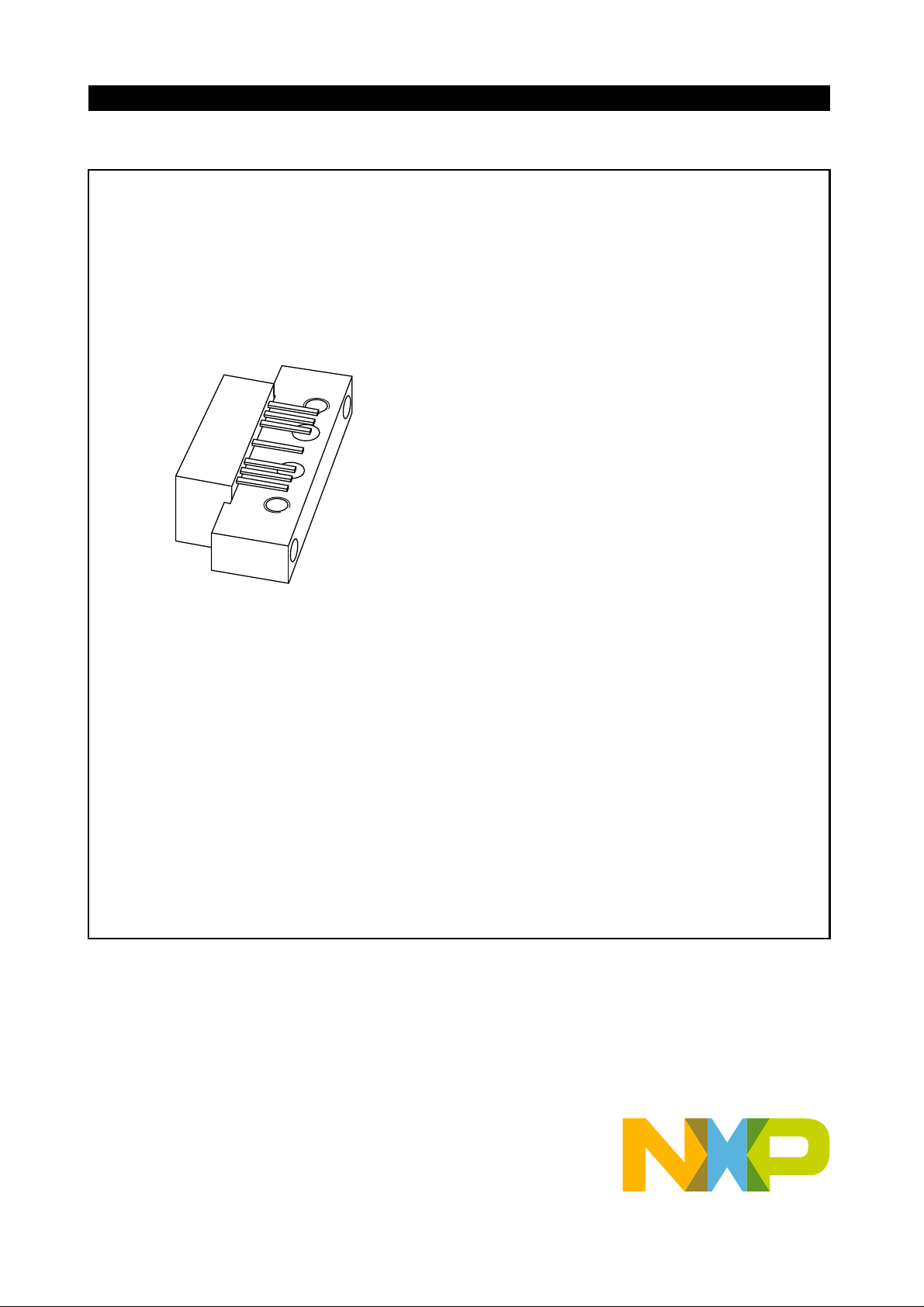
Fig.1 Simplified outline.
789
2
351
Side view
MSA319
550 MHz, 27 dB gain push-pull amplifier BGY587B
FEATURES
Excellent linearity
Extremely low noise
Silicon nitride passivation
Rugged construction
TiPtAu metallized crystals ensure
optimal reliability.
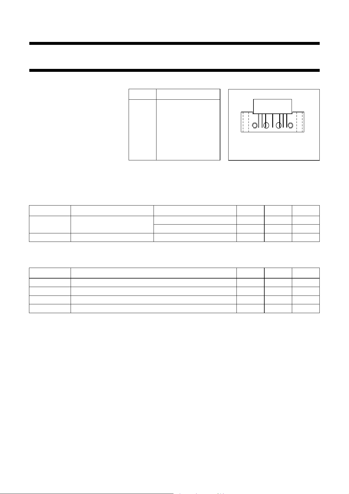
PINNING - SOT115J PIN CONFIGURATION
PIN DESCRIPTION
1 input
2 common
3 common
5+V
B
7 common
8 common
DESCRIPTION
9 output
Hybrid amplifier module for CATV
systems operating over a frequency
range of 40 to 550 MHz at a voltage
supply of +24 V (DC).
QUICK REFERENCE DATA
SYMBOL PARAMETER CONDITIONS MIN. MAX. UNIT
G
p
power gain f = 50 MHz 26.2 27.8 dB
f = 550 MHz 27.5 dB
I
tot
total current consumption (DC) VB=+24V 340 mA
LIMITING VALUES
In accordance with the Absolute Maximum Rating System (IEC 601 34).
SYMBOL PARAMETER MIN. MAX. UNIT
V
i
T
stg
T
mb
V
B
RF input voltage 55 dBmV
storage temperature 40 +100 C
operating mounting base temperature 20 +100 C
DC supply voltage +28 V
2001 Oct 22 2
NXP Semiconductors Product specification
550 MHz, 27 dB gain push-pull amplifier BGY587B
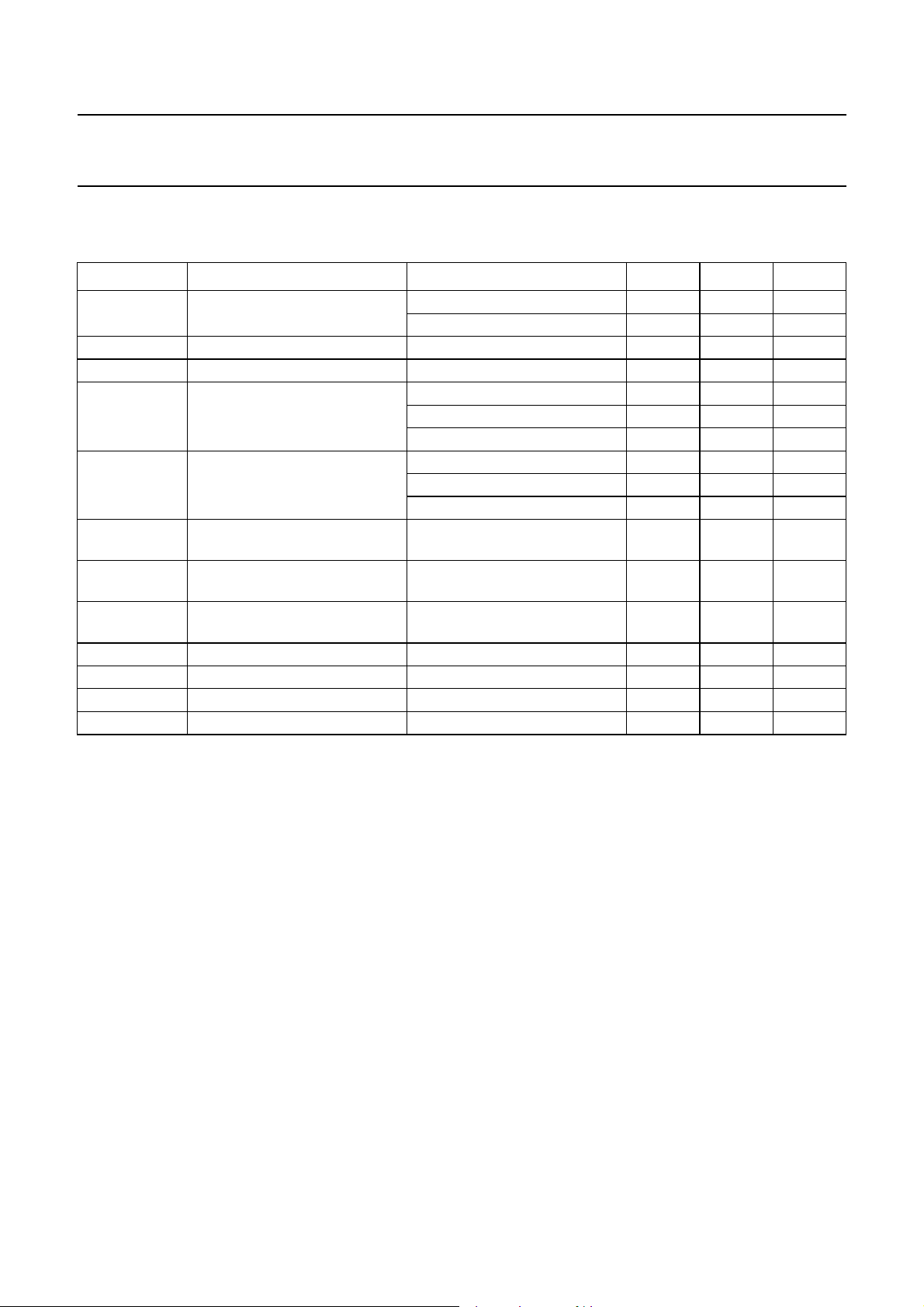
CHARACTERISTICS
Table 1 Bandwidth 40 to 550 MHz; T
=30C; ZS=ZL=75
case
SYMBOL PARAMETER CONDITIONS MIN. MAX. UNIT
G
p
power gain f = 50 MHz 26.2 27.8 dB
f = 550 MHz 27.5 dB
SL slope cable equivalent f = 40 to 550 MHz 0.5 2.5 dB
FL flatness of frequ ency response f = 40 to 550 MHz 0.4 dB
S
11
input return losses f=40to80MHz 20 dB
f = 80 to 160 MHz 19 dB
f=160to550MHz 18 dB
S
22
output return losses f = 40 to 80 MHz 20 dB
f = 80 to 160 MHz 19 dB
f=160to550MHz 18 dB
CTB composite triple beat 77 channels flat; V
=44dBmV;
o
57 dB
measured at 547.25 MHz
X
mod
cross modulation 77 channels flat; Vo=44dBmV;
60 dB
measured at 55.25 MHz
CSO composite second order
distortion
d
2
V
o
second order distortion note 1 68 dB
output voltage dim= 60 dB; note 2 61 dBmV
77 channels flat; V
=44dBmV;
o
measured at 548.5 MHz
57 dB
F noise figure f = 550 MHz 6.5 dB
I
tot
total current consumption DC value; VB= +24 V; note 3 340 mA
Notes
= 55.25 MHz; Vp= 44 dBmV;
1. f
p
=493.25MHz; Vq= 44 dBmV;
f
q
measured at f
= 548.5 MHz.
p+fq
2. Measured according to DIN45004B;
=540.25MHz; Vp=Vo= 66.5 dBmV;
f
p
f
=547.25MHz; Vq=Vo6dB;
q
= 549.25 MHz; Vr=Vo6dB;
f
r
measured at f
fr=538.25MHz.
p+fq
3. The module normally operates at V
= +24 V, but is able to withstand supply transients up to +30 V.
B
2001 Oct 22 3
 Loading...