

Page 1

UM10480
Variable gain amplifier BGA7210
Rev. 2 — 26 July 2011 User manual
Document information
Info Content
Keywords BGA7210, VGA, variable gain amplifier
Abstract This user manual describes how to evaluate the variable gain amplifier
BGA7210 using a customer evaluation kit
Page 2

NXP Semiconductors
UM10480
Variable gain amplifier BGA7210
Revision history
Rev Date Description
v.2 20110726
• Section 1 “Introduction” text altered.
• Section 5 “Controlling the customer RF evaluation board” amended to include Section
5.1 “Improving linearity”
v.1 20110520 first version
Contact information
For more information, please visit: http://www.nxp.com
For sales office addresses, please send an email to: salesaddresses@nxp.com
UM10480 All information provided in this document is subject to legal disclaimers. © NXP B.V. 2011. All rights reserved.
User manual Rev. 2 — 26 July 2011 2 of 13
Page 3
NXP Semiconductors
1. Introduction
The BGA7210 customer evaluation kit enable s the use r to ev aluat e th e pe rf or ma n ce of
the variable gain amplifier BGA7210.
The BGA7210 performance information is available in the BGA7210 data sheet.
2. Quick start
1. Connect the interface board to the RF evaluation board using the flat cable.
2. Power the RF evaluation board with a 5 V, 1 W power supply.
3. Insert the interface board in a free USB slot.
4. Insert the USB flash drive in another free USB slot.
5. Launch the customer software bga7210_mswin.exe from the USB flash drive.
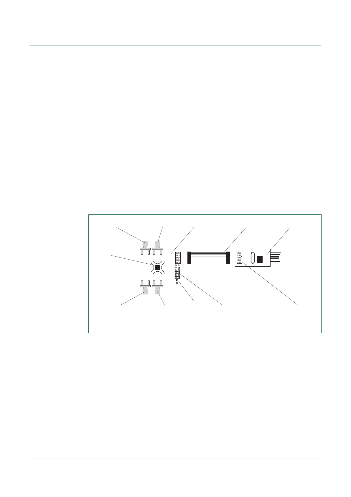
3. Installation
UM10480
Variable gain amplifier BGA7210
USB interface boardflat cableRF evaluation boardcalibration port RF in
BGA7210
GND
RF out
Fig 1. BGA7210 customer evaluation kit parts
V
supply
jumpers
connectorcalibration port
019aac406
Remark: Do not change the jumper settings until you are familiar with the functions. The
jumpers are intended for evaluating the current on each su pply pin. If configured correctly
the VGA can be powered by the USB bus, however RF performance might be
compromised. See Section 7 “
Jumpers and connectors” on page 10.
UM10480 All information provided in this document is subject to legal disclaimers. © NXP B.V. 2011. All rights reserved.
User manual Rev. 2 — 26 July 2011 3 of 13
Page 4

NXP Semiconductors
4. Customer evaluation kit contents
The evaluation kit contains the following items:
• ESD safe casing
• RF evaluation board
• USB interface board
• Flat cable
• USB flash drive containing:
– This user manual
– Customer software bga7210_mswin.exe
– BGA7210 data sheet
UM10480
Variable gain amplifier BGA7210
UM10480 All information provided in this document is subject to legal disclaimers. © NXP B.V. 2011. All rights reserved.
User manual Rev. 2 — 26 July 2011 4 of 13
Page 5

NXP Semiconductors
5. Controlling the customer RF evaluation board
5.1 Improving linearity
The RF evaluation board is configured without using a shunt capacitor on the output.
Adding a shunt capacitor improves linearity around 2.8 GHz. For other operating
frequencies it is recommended not to add a shunt capacitor. Please refer to the Data
Sheet for performance information.
Place a shunt capacitor of 0.68 pF at a distance of 5.3 mm from the BGA7210 RF_OUT
pin, see Figure 2
.
UM10480
Variable gain amplifier BGA7210
aaa-000268
Fig 2. BGA7210 RF evaluation board PCB layout
UM10480 All information provided in this document is subject to legal disclaimers. © NXP B.V. 2011. All rights reserved.
User manual Rev. 2 — 26 July 2011 5 of 13
Page 6

NXP Semiconductors
019aac407
increase attenuation
attenuation slider
decrease attenuation
power save mode
attenuation entryamplifier 2 currentamplifier 1 current
set optimal currents device versionUSB statuswrite status
5.2 Quick tour
UM10480
Variable gain amplifier BGA7210
Fig 3. User interface
The customer software offers advanced features for controlling the current and
attenuation of the BGA7210. The software also provides a tick box for saving power and a
tick box for automatically selecting the optimal current per attenuation setting, yielding
maximum linearity.
5.3 Setting current
The current to each amplifier can be set either automatically or manually.
• Automatically: depending on the attenuator setting, each amplifier current setting is
selected automatically. This mode optimizes current consumption without
compromising linearity
• Manually: each amplifier current can be set manually
5.4 Setting attenuation
There are three methods available for setting attenuation in the range 0 dB to 31.5 dB
using:
• the attenuator entry
• attenuation slider
• 0.5 dB step button
5.5 Power save
In Power save mode, the RF blocks are switched off but it is still possible to communicate
with the chip.
UM10480 All information provided in this document is subject to legal disclaimers. © NXP B.V. 2011. All rights reserved.
User manual Rev. 2 — 26 July 2011 6 of 13
Page 7

NXP Semiconductors
P
out
dBmPindBms21dB+=
019aac408
OPTIONAL
PRE-AMPLIFIER
POWER
SUPPLY
MMIC
DUT
PORT 1 PORT 2
2 PORT (or 4 PORT) NETWORK ANALYZER
OPTIONAL
ATTENUATOR
6. BGA7210 evaluation
Remark: The RF evaluation board output is configured with a shunt capacitor to yield
optimal linearity at approximately 2 GHz. It is recommended that the shunt capacitor is
removed at other operating frequencies. Please refer to the BGA7210 data sheet for
performance information.
6.1 Calibration
The calibration port can be used to determine the PCB losses.
6.2 S-parameters and output compression point
Both S-parameters and the output compression point (P1 dB) are measured with a
NetWork Analyzer (NWA); see Figure 4
The P1 dB is measured by sweeping the input power , and observing where the S21 of th e
device is compressed by 1 dB compared to the linear gain. In order for th is measureme nt
to accurately measure the input power, the input must first be calibrated with a power
head. The output power of the device is calculated using equation Equation 1
UM10480
Variable gain amplifier BGA7210
.
.
(1)
The drive power can be optionally enhanced with a driver amplifier. To prevent the output
signal driving the NWA receiver into compression, an attenuator can be inser te d at the
NWA input. Both driver amplifier and attenuator should be included in the calibration path.
Fig 4. S-parameter and output compression power set-up
In order to maintain small signal conditions for the S-parameter measurements, an input
power of 20 dBm is applied.
UM10480 All information provided in this document is subject to legal disclaimers. © NXP B.V. 2011. All rights reserved.
User manual Rev. 2 — 26 July 2011 7 of 13
Page 8

NXP Semiconductors
019aac410
POWER
SUPPLY
MMIC
DUT
SIGNAL
GENERATOR
SIGNAL
GENERATOR
ISOLATOR
LOW-PASS
FILTER (LPF)
POWER
COMBINER
SPECTRUM
ANALYZER
ISOLATOR
LOW-PASS
FILTER (LPF)
6.3 Output third-order intercept point
The output intercept point (OIP3) is a figure of merit for linearity; see Figure 5. The set-up
is configured to achieve an accurate measurement of the OIP3; see Figure 6
signal generators, a Low-Pass Filter (LPF) and isolator is applied, before combining the
two signals. This configuration gives best isolation between the generators, hence IMD3
levels of the input signal < 80 dBc can be measured.
Please refer to the BGA7210 data sheet for power level and tone spacing values.
dBc
output
power
fundamental
slope 1:1
UM10480
Variable gain amplifier BGA7210
. After the
IP3
saturation
region
IMD3
slope 1:3
dBc
IMD3
2*f1-f2f1f
2
1
f2*f2-f
input power
019aac409
Fig 5. Definition of output intercept point (OIP3)
Fig 6. Output intercept point (OIP3) set-up
UM10480 All information provided in this document is subject to legal disclaimers. © NXP B.V. 2011. All rights reserved.
User manual Rev. 2 — 26 July 2011 8 of 13
Page 9

NXP Semiconductors
6.4 Noise
The Noise Figure (NF) is measured using a calibrated noise source with a specified
Excess Noise Ratio (ENR), and a spectrum analyzer with a noise measurement option.
The system is calibrated with this noise source in order to measure accurate noise figures;
see Figure 7
UM10480
Variable gain amplifier BGA7210
.
POWER
SUPPLY
NOISE
SOURCE
Fig 7. Noise figure measurement set-up
DUT
MMIC
SPECTRUM
ANALYZER
including
NOISE OPTION
019aac411
UM10480 All information provided in this document is subject to legal disclaimers. © NXP B.V. 2011. All rights reserved.
User manual Rev. 2 — 26 July 2011 9 of 13
Page 10

NXP Semiconductors
7. Jumpers and connectors
UM10480
Variable gain amplifier BGA7210
019aac412
Fig 8. BGA7210 RF evaluation board jumpers and connectors
Table 1. RF evaluation board components
Component reference Description
RF connectors
X6, X7 calibration port for determining PCB losses
X1 RF in
X5 RF out
Control interface
X2 USB interface board connector
Voltage sup ply
X4 external supply voltage 5 V/200 mA
X3 power configuration jumper
The RF evaluation board is powered through connector X4. The X3 jumpers are set as
shown in Figure 9
UM10480 All information provided in this document is subject to legal disclaimers. © NXP B.V. 2011. All rights reserved.
User manual Rev. 2 — 26 July 2011 10 of 13
.
Page 11

NXP Semiconductors
019aac413
VRFO
VCC2
VDDA
VCC1
VDDD
VUSB
X3
019aac414
VRFO
VCC2
VDDA
VCC1
VDDD
VUSB
X3
Fig 9. X3 jumper setting using supply voltage on X4
The 5 V provided by the USB port can be used for quick tests. In that case X4 should not
be used and jumpers on X3 should be set as shown in Figure 10
UM10480
Variable gain amplifier BGA7210
.
Fig 10. X3 jumper setting using USB supply voltage on X2
8. Abbreviations
Table 2. Abbreviations
Acronym Description
DUT Device Under Test
ESD ElectroStatic Discharge
IMD3 Inter-Modulation Distortion (third-order)
MMIC Monolithic Microwave Integrated Circuit
PCB Printed-Circuit Board
USB Universal Serial Bus
VGA Variable Gain Amplifier
UM10480 All information provided in this document is subject to legal disclaimers. © NXP B.V. 2011. All rights reserved.
User manual Rev. 2 — 26 July 2011 11 of 13
Page 12

NXP Semiconductors
9. Legal information
UM10480
Variable gain amplifier BGA7210
9.1 Definitions
Draft — The document is a draft version only. The content is still under
internal review and subject to formal approval, which may result in
modifications or additions. NXP Semiconductors does not give any
representations or warranties as to the accuracy or completeness of
information included herein and shall have no liability for the consequences of
use of such information.
9.2 Disclaimers
Limited warranty and liability — Information in this document is believed to
be accurate and reliable. However, NXP Semiconductors does not give any
representations or warranties, expressed or implied, as to the accuracy or
completeness of such information and shall have no liability for the
consequences of use of such information.
In no event shall NXP Semiconductors be liable for any indirect, incidental,
punitive, special or consequential damages (including - without limitation - lost
profits, lost savings, business interruption, costs related to the removal or
replacement of any products or rework charges) whether or not such
damages are based on tort (including negligence), warranty, breach of
contract or any other legal theory.
Notwithstanding any damages that customer might incur for any reason
whatsoever, NXP Semi conductors’ aggregat e and cumulative liabil ity towards
customer for the products described herein shall be limited in accordance
with the Terms and conditions of commercial sale of NXP Semiconductors.
Right to make changes — NXP Semiconductors reserves the right to make
changes to information published in this document, including without
limitation specifications and product descriptions, at any time and without
notice. This document supersedes and replaces all information supplied prior
to the publication hereof.
Suitability for use — NXP Semiconductors products are not designed,
authorized or warranted to be suitable for use in life support, life-critical or
safety-critical systems or equipment, nor in applications where failure or
malfunction of an NXP Semiconductors product can reasonably be expected
to result in personal injury, death or severe property or environmental
damage. NXP Semiconductors accepts no liability for inclusion and/or use of
NXP Semiconductors products in such equipment or applica tions and
therefore such inclusion and/or use is at the customer’s own risk.
Applications — Applications that are described herein for any of these
products are for illustrative purposes only. NXP Semiconductors makes no
representation or warranty that such applications will be suitable for the
specified use without further testing or modification.
Customers are responsible for the design and operation of their applications
and products using NXP Semiconductors product s, and NXP Semiconductors
accepts no liability for any assistance with applications or customer product
design. It is customer’s sole responsibility to determine whether the NXP
Semiconductors product is suitable and fit for the customer’s applications and
products planned, as well as for the planned application and use of
customer’s third party customer(s). Customers should provide appropriate
design and operating safeguards to minimize the risks associated with their
applications and products.
NXP Semiconductors does not accept any liability related to any default ,
damage, costs or problem which is based on any weakness or default in the
customer’s applications or products, or the application or use by customer’s
third party customer(s). Customer is responsible for doing all necessary
testing for the customer’s applications and products using NXP
Semiconductors products in order to avoid a default of the applications and
the products or of the application or use by customer’s third part y
customer(s). NXP does not accept any liability in this respect.
Export control — This document as well as the item(s) described herein
may be subject to export control regulations. Export might require a prior
authorization from national authorities.
Evaluation products — This product is provided on an “as is” and “with all
faults” basis for evaluation purposes only. NXP Semiconductors, its affiliates
and their suppliers expressly disclaim all warranties, whet her express, implied
or statutory, including but not limited to the implied warranties of
non-infringement, merchantability and fitness for a particular purpose. The
entire risk as to the quality, or arising out of the use or performance, of this
product remains with customer.
In no event shall NXP Semiconductors, its affiliates or their su ppliers be liable
to customer for any special, indirect, consequential, punitive or incidental
damages (including without limitation damages for l oss of bu siness, busi ness
interruption, loss of use, loss of data or information, and the like) arising out
the use of or inability to use the product, whether or not based on tort
(including negligence), strict liability, breach of contract, breach of warranty or
any other theory , even if advised of the possibility of such damages.
Notwithstanding any damages that customer might incur for any reason
whatsoever (including without limitation, all damages referenced above and
all direct or general damages), the entire liability of NXP Semiconductors, its
affiliates and their suppliers and customer’s exclusive remedy for all of the
foregoing shall be limited to actual damages incurred by customer based on
reasonable reliance up to the greater of the amount actually paid by customer
for the product or five dollars (US$5.00). The foregoin g limita tions, exclusions
and disclaimers shall apply to the maximum extent permitted by applicable
law, even if any remedy fails of its essential purpose.
9.3 Trademarks
Notice: All referenced brands, prod uct names, service names and trademarks
are the property of their respective owners.
UM10480 All information provided in this document is subject to legal disclaimers. © NXP B.V. 2011. All rights reserved.
User manual Rev. 2 — 26 July 2011 12 of 13
Page 13

NXP Semiconductors
10. Contents
1 Introduction . . . . . . . . . . . . . . . . . . . . . . . . . . . . 3
2 Quick start . . . . . . . . . . . . . . . . . . . . . . . . . . . . . 3
3 Installation . . . . . . . . . . . . . . . . . . . . . . . . . . . . . 3
4 Customer evaluation kit contents . . . . . . . . . . 4
5 Controlling the customer RF evaluation board 5
5.1 Improving linearity . . . . . . . . . . . . . . . . . . . . . . 5
5.2 Quick tour . . . . . . . . . . . . . . . . . . . . . . . . . . . . . 6
5.3 Setting current . . . . . . . . . . . . . . . . . . . . . . . . . 6
5.4 Setting attenuation . . . . . . . . . . . . . . . . . . . . . . 6
5.5 Power save. . . . . . . . . . . . . . . . . . . . . . . . . . . . 6
6 BGA7210 evaluation . . . . . . . . . . . . . . . . . . . . . 7
6.1 Calibration . . . . . . . . . . . . . . . . . . . . . . . . . . . . 7
6.2 S-parameters and output compression point . . 7
6.3 Output third-order intercept point . . . . . . . . . . . 8
6.4 Noise . . . . . . . . . . . . . . . . . . . . . . . . . . . . . . . . 9
7 Jumpers and connectors . . . . . . . . . . . . . . . . 10
8 Abbreviations. . . . . . . . . . . . . . . . . . . . . . . . . . 11
9 Legal information. . . . . . . . . . . . . . . . . . . . . . . 12
9.1 Definitions. . . . . . . . . . . . . . . . . . . . . . . . . . . . 12
9.2 Disclaimers. . . . . . . . . . . . . . . . . . . . . . . . . . . 12
9.3 Trademarks. . . . . . . . . . . . . . . . . . . . . . . . . . . 12
10 Contents . . . . . . . . . . . . . . . . . . . . . . . . . . . . . . 13
UM10480
Variable gain amplifier BGA7210
Please be aware that important notices concerning this document and the product(s)
described herein, have been included in section ‘Legal information’.
© NXP B.V. 2011. All rights reserved.
For more information, please visit: http://www.nxp.com
For sales office addresses, please send an email to: salesaddresses@nxp.com
Date of release: 26 July 2011
Document identifier: UM10480
 Loading...