

NXP Semiconductors BGA2003 Datasheet
DATA SH EET
DISCRETE SEMICONDUCTORS
M3D124
BGA2003
Silicon MMIC amplifier
Product specification
Supersedes data of 1999 Jul 23
2010 Sep 13
NXP Semiconductors Product specification
Silicon MMIC amplifier BGA2003
FEATURES
• Low current
• Very high power gain
• Low noise figure
• Integrated temperature compensated biasing
• Control pin for adjustment bias current
• Supply and RF output pin combined.
APPLICATIONS
• RF front end
• Wideband applications, e.g. analog and digital cellular
telephones, cordless telephones (PHS, DECT, etc.)
• Low noise amplifiers
• Satellite television tuners (SATV)
• High frequency oscillators.
DESCRIPTION
Silicon MMIC amplifier consisting of an NPN double
polysilicon transistor with integrated biasing for low voltage
applications in a plastic, 4-pin SOT343R package.
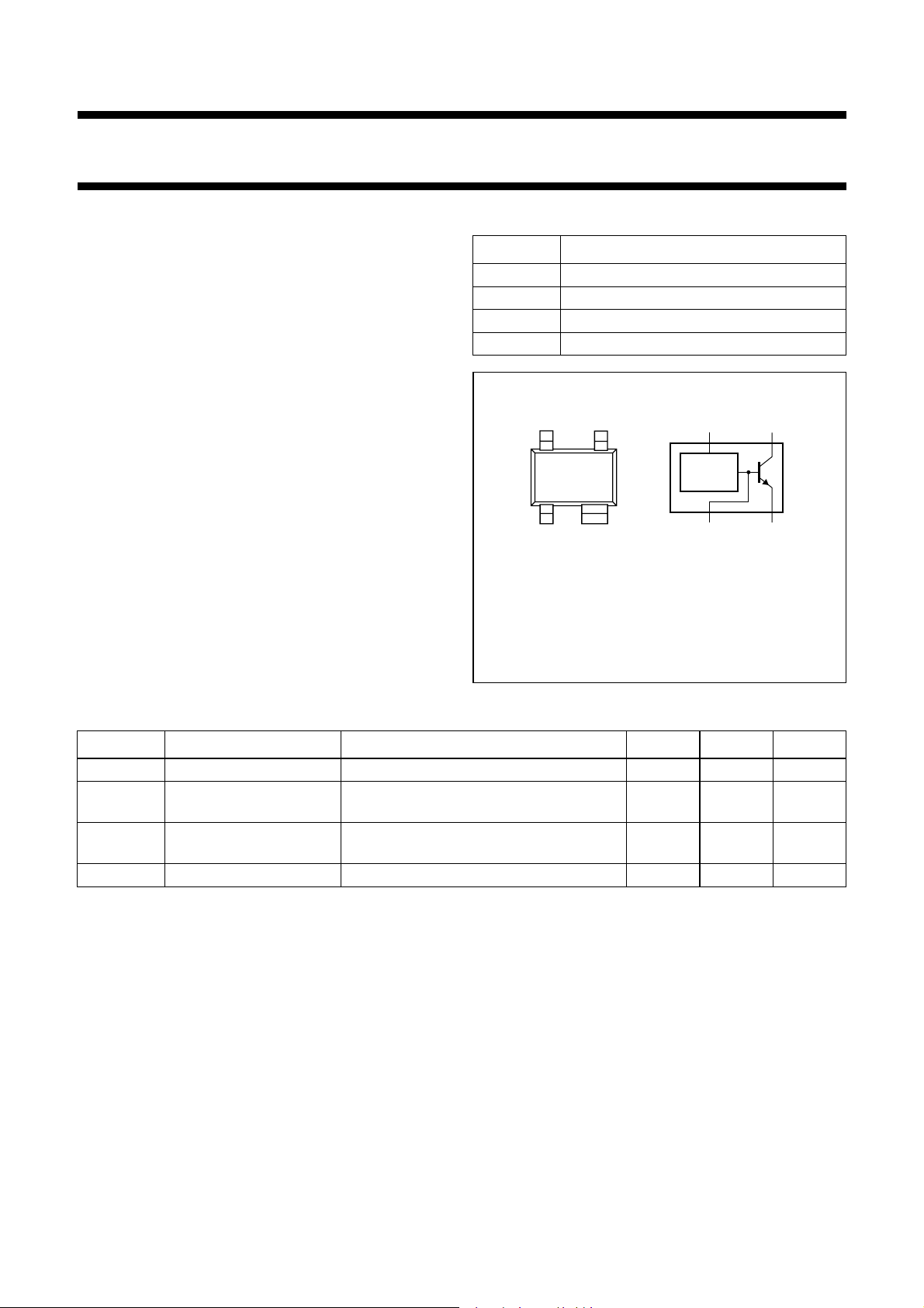
PINNING
PIN DESCRIPTION
1GND
2RF in
3 CTRL (bias current control)
4V
handbook, halfpage
21
Top view MAM427
Marking code: A3*
+ RF out
S
43
CTRL
BIAS
CIRCUIT
RFin GND
* = - : made in Hong Kong
* = p : made in Hong Kong
* = t : made in Malaysia
Fig.1 Simplified outline (SOT343R) and symbol.
VS+RFout
QUICK REFERENCE DATA
SYMBOL PARAMETER CONDITIONS TYP. MAX. UNIT
V
S
I
S
DC supply voltage RF input AC coupled − 4.5 V
DC supply current V
VS-OUT
= 2.5 V; I
CTRL
=1mA;
11 − mA
RF input AC coupled
MSG maximum stable gain V
T
NF noise figure V
= 2.5 V; f = 1800 MHz;
VS-OUT
=25°C
amb
= 2.5 V; f = 1800 MHz; ΓS= Γ
VS-OUT
16 − dB
1.8 − dB
opt
2010 Sep 13 2
NXP Semiconductors Product specification
Silicon MMIC amplifier BGA2003
LIMITING VALUES
In accordance with the Absolu te Maximum Rating System (IEC 1 34).
SYMBOL PARAMETER CONDITIONS MIN. MAX. UNIT
V
S
V
CTRL
I
S
I
CTRL
P
tot
T
stg
T
j
THERMAL CHARACTERISTICS
SYMBOL PARAMETER VALUE UNIT
R
th j-s
supply voltage RF input AC coupled − 4.5 V
voltage on control pin − 2V
supply current (DC) forced by DC voltage on RF input
or I
CTRL
− 30 mA
control current − 3mA
total power dissipation Ts≤ 100 °C − 135 mW
storage temperature −65 +150 °C
operating junction temperature − 150 °C
thermal resistance from junction to soldering point 350 K/W
CHARACTERISTICS
RF input AC coupled; T
=25°C; unless otherwise specified.
j
SYMBOL PARAMETER CONDITIONS MIN. TYP. MAX. UNIT
I
S
MSG maximum stable gain V
supply current V
VS-OUT
V
VS-OUT
VS-OUT
= 2.5 V; I
= 2.5 V; I
= 2.5 V; I
= 0.4 mA 3 4.5 6 mA
CTRL
=1.0mA 8 11 15 mA
CTRL
VS-OUT
=10mA;
− 24 − dB
f=900MHz
V
VS-OUT
= 2.5 V; I
VS-OUT
=10mA;
− 16 − dB
f=1800MHz
2
|s
|
21
insertion power gain V
VS-OUT
= 2.5 V; I
VS-OUT
=10mA;
18 19 − dB
f=900MHz
V
VS-OUT
= 2.5 V; I
VS-OUT
=10mA;
13 14 − dB
f=1800MHz
s
12
isolation V
VS-OUT
= 2.5 V; I
VS-OUT
=0;
− 26 − dB
f=900MHz
V
VS-OUT
= 2.5 V; I
VS-OUT
=0;
− 20 − dB
f=1800MHz
NF noise figure V
IP3
(in)
input intercept point; note 1 V
= 2.5 V; I
VS-OUT
f=900MHz; Γ
VS-OUT
= 2.5 V; I
V
f=1800MHz; Γ
= 2.3 V; I
VS-OUT
= Γ
S
S
VS-OUT
opt
VS-OUT
= Γ
opt
VS-OUT
=10mA;
=10mA;
=3.6mA;
− 1.8 2 dB
− 1.8 2 dB
−−6.5 − dBm
f=900MHz
V
VS-OUT
= 2.3 V; I
VS-OUT
=3.5mA;
−−4.8 − dBm
f=1800MHz
Note
1. See application note RNR-T45-99-B-0514.
2010 Sep 13 3
NXP Semiconductors Product specification
Silicon MMIC amplifier BGA2003
handbook, halfpage
V
CTRL
100 pF
R
CTRL
BGA2003
2
C
RF in
R1
L1
C
43
1
MGS536
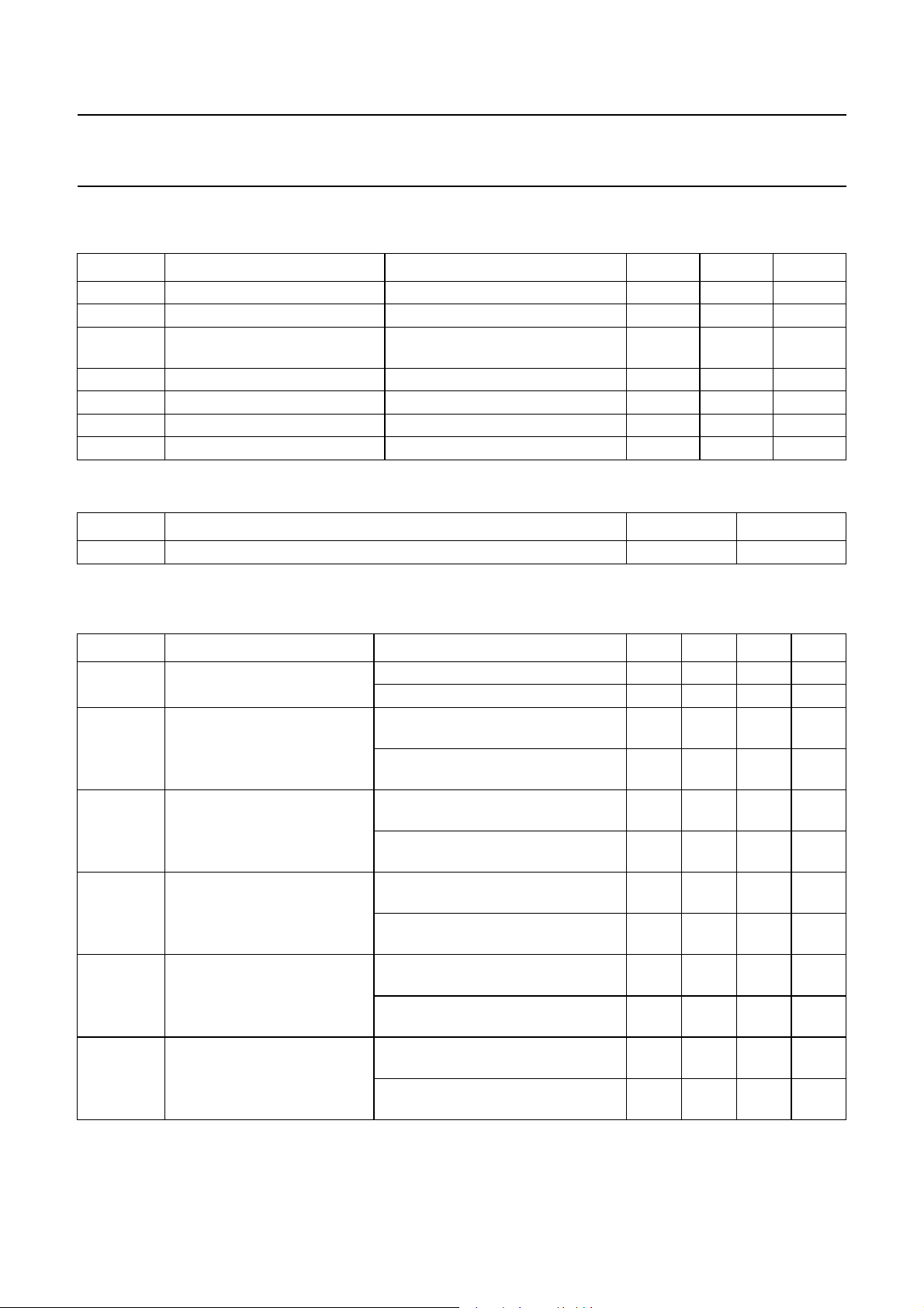
Fig.2 Typical application circuit.
V
S
RF out
200
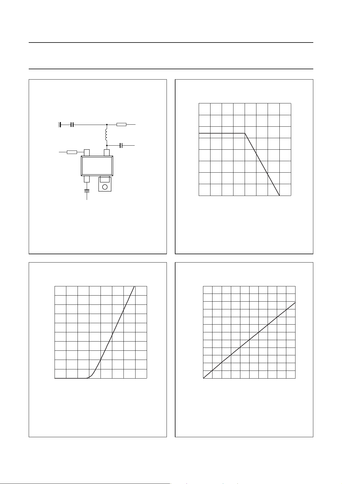
handbook, halfpage
P
tot
(mW)
150
100
50
0
0 50 100 200
150
Fig.3 Power derating.
Ts (
MGS537
°C)
1.5
V
CTRL
MGS538
(V)
2.5
handbook, halfpage
I
CTRL
(mA)
2
1.5
1
0.5
0
0 0.5 1 2
I
=(V
CTRL
CTRL
− 0.83)/296.
Fig.4 Control current as a function of the control
voltage on pin 3; typical values.
30
handbook, halfpage
I
VS-OUT
(mA)
20
10
0
0 2.5
V
S-OUT
0.5 1 1.5 2
=2.5V.
I
Fig.5 Bias current as a function of the control
current; typical values.
CTRL
MGS539
(mA)
2010 Sep 13 4
 Loading...