Page 1

SiGeC microwave NPN
transistor BFU725F
A perfect match up to 20 GHz
Meet the trend towards higher frequencies. With NXP Semiconductors’ latest SiGeC microwave
NPN transistor BFU725F, you get high switching frequencies plus extremely high gain and low noise.
All this in an easy-to-use SOT343F package. It’s the ideal solution for applications up to 20 GHz.
Key features
Ñ
Very low noise (0.4 dB at 1.8 GHz / 0.67 dB at 5.8 GHz)
Ñ
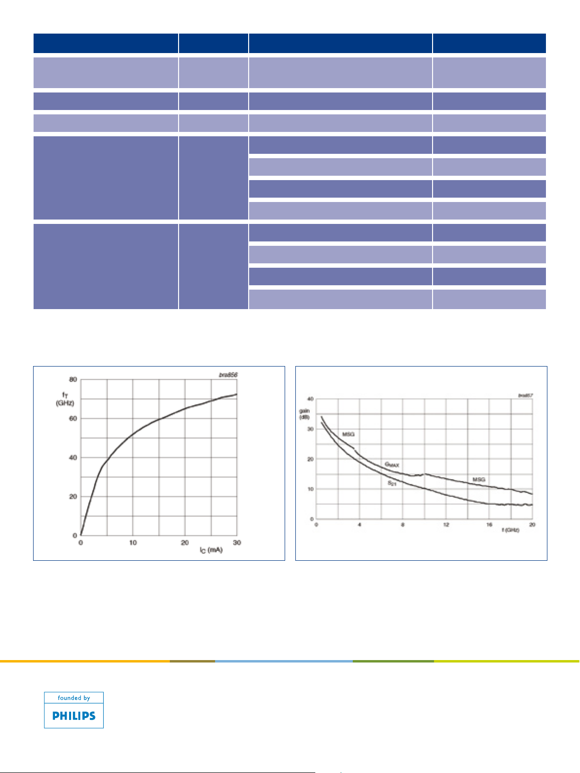
High maximum stable gain (27.8 dB at 1.8 GHz / 10 dB
at 18 GHz)
Ñ
High switching frequency (fT >100 GHz / f
Ñ
Plastic surface-mount SOT343F package
Key benefi ts
Ñ
SiGeC process delivers high switching frequency from
a silicon-based device
Ñ
Cost-effective alternative to GaAs devices
Ñ
RoHS compliant
Key applications
Ñ
GPS systems
Ñ
DECT phones
Ñ
Low noise amplifi er (LNA) for microwave
communications systems
Ñ
2nd stage LNA and mixer in direct broadcast satellite (DBS)
low-noise blocks (LNBs)
Ñ
Satellite radio
Ñ
WLAN and CDMA applications
Ñ
Low-noise microwave applications
>150 GHz)
MAX
The NPN microwave transistor BFU725F delivers an unbeatable
blend of high switching frequency, high gain and very low
noise. Thanks to its ultra-low noise fi gure, it’s perfect for your
sensitive RF receivers particularly those for high-performance
cell phones. Alternatively, with its high cut-off frequency,
it’s your ideal solution for microwave applications in the 10 GHz
to 30 GHz range, such as satellite TV receivers and automotive
collision avoidance radar.
The BFU725F get its outstanding performance from our
innovative silicon-germanium-carbon (SiGeC) BiCMOS
process. QUBiC4X was designed specifi cally to meet the
needs of real-life, high-frequency applications and delivers
an unrivalled fusion of high power gain and excellent dynamic
range. It combines the performance of gallium-arsenide (GaAs)
technologies with the reliability of a silicon-based process.
In addition, with the BFU725F, you don’t need a biasing IC or
negative biasing voltage. So it’s a much more cost-effective
solution than GaAs pHEMT devices.
Page 2

Parameter Symbol Conditions Value
Collector-emitter breakdown
BV
CEO
voltage
Maximum collector current I
Transition frequency f
C(max)
T
Noise figure NF
Maximum stable power gain MSG / G
Quick reference data
P(max)
IC = 1 mA; IB = 0 3.2 V
40 mA
VCE = 2 V; IC = 25 mA; f = 2 GHz 68 GHz
VCE = 2 V; IC = 5 mA; f = 1.8 GHz; Γs = Γ
VCE = 2 V; IC = 5 mA; f = 2.4 GHz; Γs = Γ
VCE = 2 V; IC = 5 mA; f = 5.8 GHz; Γs = Γ
VCE = 2 V; IC = 5 mA; f = 12 GHz; Γs = Γ
opt
opt
opt
opt
0.4 dB
0.45 dB
0.7 dB
1.0 dB
VCE = 2 V; IC = 25 mA; f = 1.8 GHz 26.6 dB
VCE = 2 V; IC = 25 mA; f = 2.4 GHz 25.5 dB
VCE = 2 V; IC = 25 mA; f = 12 GHz 13 dB
VCE = 2 V; IC = 25 mA; f = 5.8 GHz 17 dB
Transition frequency as a function of collector current (typical values) Gain as a function of frequency (typical values)
www.nxp.com
©200 6 NXP B.V.
All right s res erved. Reprod uction in whole or in part is prohibi ted w ithout the prior writ ten consent of the copyrig ht o wner.
The informa tion presented in this documen t doe s not form part of any quotation or contra ct, is bel ieved to be accur ate a nd
reliab le a nd may be c hanged witho ut notice. No liabilit y will be accepted by the publ isher for any conseq uence of its use.
Public ation there of does not conv ey nor imply any l icense unde r patent- or othe r industri al or intellec tual proper ty right s.
Date of rel ease: Octob er 2006
Docum ent order num ber: 9397 750 1578 4
Printe d in the Nether lands
 Loading...