

Page 1

AN10881
TEA1713 resonant power supply control IC with PFC
Rev. 2 — 26 September 2011 Application note
Document information
Info Content
Keywords TEA1713, adapter, LCD TV, Plasma TV, resonant, converter, PFC,
Burst mode
Abstract The TEA1713 integrates a controller for Power Factor Correction (PFC)
and a controller for a half-bridge resonant converter (HBC).
It provides the drive function for the discrete MOSFET for the up-converter
and for the two discrete power MOSFETs in a resonant half-bridge
configuration.
The resonant controller part is a high-voltage controller for a zero voltage
switching LLC resonant converter. The resonant controller part of the IC
includes a high-voltage level shift circuit and several protection features
such as overcurrent protection, open-loop protection, Capacitive mode
protection and a general purpose latched protection input.
In addition to the resonant controller, the TEA1713 also contains a Power
Factor Correction (PFC) controller. The efficient operation of the PFC is
obtained by functions such as quasi-resonant operation at high power
levels and quasi-resonant operation with valley skipping at lower power
levels. Overcurrent protection, overvoltage protection and
demagnetization sensing, ensures safe operation in all conditions.
The proprietary high-voltage BCD Powerlogic process makes direct
start-up possible from the rectified universal mains voltage in an efficient
way. A second low voltage Silicon-On-Insulator (SOI) IC is used for
accurate, high speed protection functions and control.
The combination of PFC and a resonant controller in one IC makes the
TEA1713 suitable for power supplies in LCD TV, plasma televisions, PC
power supplies, high-power office equipment and adapters.
This application note discusses the TEA1713 functions for applications.
Page 2

NXP Semiconductors
AN10881
TEA1713 resonant power supply control IC with PFC
Table 1. Revision history
Rev Date Description
02 20110926 Second, updated release
01 20100322 First release
Contact information
For more information, please visit: http://www.nxp.com
For sales office addresses, please send an email to: salesaddresses@nxp.com
AN10881 All information provided in this document is subject to legal disclaimers. © NXP B.V. 2011. All rights reserved.
Application note Rev. 2 — 26 September 2011 2 of 102
Page 3

NXP Semiconductors
1. Introduction
1.1 Scope and setup
This application note discusses the TEA1713 functions for applications in general.
Because the TEA1713 provides extensive functionality, many subjects are discussed.
This document is set up in such a way, that a chapter or paragraph of a selected subject
can be read as a standalone explanation with a minimum of cross-references to other
document parts or the data sheet. This leads to some repetition of information within the
application note and to descriptions or figures that are similar to those published in the
TEA1713 data sheet. In most cases typical values are given to enhance the readability.
• Section 1 “Introduction”
• Section 2 “TEA1713 highlights and features”
• Section 3 “Pin overview with functional description”
• Section 4 “Application diagram and block diagrams”
• Section 5 “Supply functions”
• Section 6 “MOSFET drivers GATEPFC, GATELS and GATEHS”
• Section 7 “PFC functions”
• Section 8 “HBC functions”
• Section 9 “Burst mode operation”
• Section 10 “Protection functions”
• Section 11 “Miscellaneous advice and tips”
• Section 12 “Application examples and topologies”
• Section 13 “Differences between TEA1713T and TEA1713LT”
AN10881
TEA1713 resonant power supply control IC with PFC
An overview of the TEA1713 pins with a summary of the functionality.
Sections 6, 7, 8, 9, and 10 describe the main functions of the TEA1713, providing an
in-depth explanation of the issues relating to the subject. The functions are written
from an application point of view .
An overview of the protection functions of th e TEA1713 with an exte nded expl anation
and related issues on the subject. These functions are described and seen from an
applications point of view.
A collection of subjects related to PCB design and debugging are discussed, including
proposals for the way of working.
This section contains examples of applications (circuit diagrams) and possible
topologies.
An overview of the differences between the TEA1713T and the TEA1713LT.
Remark: All values provided throughout this document are typical values unless
otherwise stated.
AN10881 All information provided in this document is subject to legal disclaimers. © NXP B.V. 2011. All rights reserved.
Application note Rev. 2 — 26 September 2011 3 of 102
Page 4

NXP Semiconductors
1.2 Related documents
Additional information and tools can be found in other TEA1713 documents such as:
• Data sheet
• User manual of demo board
• Calculation sheet
AN10881
TEA1713 resonant power supply control IC with PFC
AN10881 All information provided in this document is subject to legal disclaimers. © NXP B.V. 2011. All rights reserved.
Application note Rev. 2 — 26 September 2011 4 of 102
Page 5

NXP Semiconductors
2. TEA1713 highlights and features
2.1 Resonant conversion
Today’s market demands high-quality, reliable, small, lightweight and efficient power
supplies.
In principle, the higher the operating frequency, the smaller and lighter the transformers,
filter inductors and capacitors can be. On the other hand, the core, switching and winding
losses of the transformer increase at higher frequencies and become dominant. This
effect reduces the efficiency at a high frequency, which limits the minimum size of the
transformer.
The corner frequency of the output filter usually determines the bandwidth of the control
loop. A well-chosen corner frequency allows high operating frequencies to achieve a fast
dynamic response.
Pulse Width Modulated (PWM) power converters, such as flyback, up and down
converters, are widely used in low and medium power applications. A disadvantage of
these converters is that the PWM rectangular voltage and current waveforms cause
turn-on and turn-off losses that limit the operating frequency. The rectangular waveforms
also generate broadband electromagnetic energy that can produce ElectroMagnetic
Interference (EMI).
AN10881
TEA1713 resonant power supply control IC with PFC
A resonant DC-to-DC converter produces sinusoidal waveforms and reduces the
switching losses, which provide the possibility of operation at higher frequencies.
Recent environmental considerations have resulted in a need for high efficiency
performance at low loads. Burst mode operation of the resonant converter can provide
this if the converter is required to remain active as is the case for adapter applications.
Why resonant conversion?
• High power
• High efficiency
• EMI friendly
• Compact
2.2 Power factor correction conversion
Most switch mode power supplies result in a non-linear impedance (load characteristic) to
the mains input. Current taken from the mains supply occurs only at the highest voltage
peaks and is stored in a large capacitor. The energy is taken from this capacitor storage,
in accordance with the switch mode power supply operation characteristics.
Government regulations dictate special requirements for the load characteristics of certain
applications. Two main requirements can be distinguished:
• Mains harmonics requirements EN61000-3-2
• Power factor (real power/apparent power)
The requirements work towards a more resistive characteristic of the mains load.
AN10881 All information provided in this document is subject to legal disclaimers. © NXP B.V. 2011. All rights reserved.
Application note Rev. 2 — 26 September 2011 5 of 102
Page 6

NXP Semiconductors
Measures are required regarding the input circuit of the power supply to fulfill these
requirements. Passive (often a series coil) or active (often a boost converter) circuits can
be used to modify the mains load characteristics accordingly.
An additional market requirement for the added mains input circuit is that it works with a
good efficiency and have a low cost.
Using a boost converter to meet these requirements provides the benefit of a fixed DC
input voltage when combined with a resonant converter. The fixed input voltage provides
easier design of the resonant converter (specially for wide mains input voltage ra nge
applications) and the possibility to reach a higher efficiency.
2.3 TEA1713 resonant power supply control IC with PFC
The TEA1713 integrates two controllers, one for Power Factor Correction (PFC) and one
for a half-bridge resonant converter (HBC). It provides the drive function for the discrete
MOSFET for the up-converter and for the two discrete power MOSFETs in a resonant
half-bridge configuration.
The resonant controller part is a high-voltage controller for a zero voltage switching LLC
resonant converter.
AN10881
TEA1713 resonant power supply control IC with PFC
The resonant controller part of the IC includes a high-volt age leve l shift circuit and severa l
protection features such as overcurrent protection, open-loop protection, Ca pacitive mode
protection and a general purpose latched protection input.
In addition to the resonant controller, the TEA1713 also contains a Power Factor
Correction (PFC) controller. The efficient operation of the PFC is obtained by functions
such as quasi-resonant operation at high power levels and quasi-resonant operation with
valley skipping at lower power levels. Overcurrent protection, overvoltage protection and
demagnetization sensing ensures safe operation in all conditions.
The proprietary high-voltage BCD Powerlogic process ma kes direct start-up possible from
the rectified universal mains voltage in an efficient way. A second internal low-voltage SOI
die is used for accurate, high-speed protection functions and control.
The topology of a PFC and a resonant converter controlled by the TEA1713 is flexible and
enables a broad range of applications for wide input (85 V to 264 V) AC mains voltages.
The combination of PFC and resonant controller in one IC makes the TEA1713 suitable
for compact power supplies with a high level of integration and functionality.
2.4 Features
2.4.1 General features
• Integrated power factor controller and resonant controller
• Universal mains supply operation
• High level of integration, resulting in a low external component count and a cost
effective design
• Enable input. Also allows enabling of PFC only
• On-chip high-voltage start-up sour ce
• Standalone operation or IC supply from external DC supply
AN10881 All information provided in this document is subject to legal disclaimers. © NXP B.V. 2011. All rights reserved.
Application note Rev. 2 — 26 September 2011 6 of 102
Page 7

NXP Semiconductors
2.4.2 Power factor controller features
• Boundary mode operation with on-time control for highest efficiency
• Valley/zero voltage switching for minimum switching losses
• Frequency limitation to reduce switching losses
• Accurate boost voltage regulation
• Burst mode switching with soft-start and soft-stop
2.4.3 Resonant half-bridge controller features
• Integrated high-voltage level shifter
• Adjustable minimum and maximum frequency
• Maximum 500 kHz half-bridge switching frequency
• Adaptive non-overlap timing
• Burst mode switching
2.4.4 Protection features
• Safe restart mode for system fault conditions
• General latched protection input for output overvoltage protection or external
• Protection timer for time-out and restart
• OverTemperature Protection (OTP)
• Soft (re)start for both converters
• Undervoltage protection for mains (brownout), boost, IC supply and output voltage
• Overcurrent regulation and protection for both converters
• Accurate overvoltage protection for boost voltage
• Capacitive mode protection for resonant converter
AN10881
TEA1713 resonant power supply control IC with PFC
temperature protection
2.5 Protection
The TEA1713 provides several protection functions that combine detection with a
response to solve the problem. By regulating the frequency as a reaction to, for example,
overpower or bad half-bridge switching, the problem can be solved or operation kept safe
until it is decided to stop and restart (timer function).
2.6 Typical areas of application
• LCD television
• Plasma television
• High-power adapters
• Slim notebook adapters
• PC power supplies
• Office equipment
AN10881 All information provided in this document is subject to legal disclaimers. © NXP B.V. 2011. All rights reserved.
Application note Rev. 2 — 26 September 2011 7 of 102
Page 8

NXP Semiconductors
TEA1713 resonant power supply control IC with PFC
3. Pin overview with functional description
AN10881
Table 2. Pinning overview
Pin Name Functional description
1 COMPPFC Frequency compensation for the PFC control-loop.
2 SNSMAINS Sense input for mains voltage.
Externally connected filter with typical values: 150 nF (33 k + 470 nF)
Externally connected to resistive divided mains voltage.
This pin has four functions:
• Mains enable level: V
start(SNSMAINS)
• Mains stop level (brownout): V
=1.15V
stop(SNSMAINS)
=0.9V
• Mains-voltage compensation for the PFC control-loop gain bandwidth
• Fast latch reset: V
The mains enable and mains stop level enable and disable the PFC. Enabling and disabling of
the resonant controller is based on the voltage on SNSBOOST.
The voltage on the SNSMAINS pin must be an averaged DC value, representing the AC line
voltage. Do not use the pin for sensing the phase of the mains voltage.
Open pin detection is included by an internal current source (33 nA).
3 SNSAUXPFC Sense input from an auxiliary winding of the PFC coil for demagnetization timing and valley
detection to control the PFC switching. It is 100 mV level with a time-out of 50 s.
Connect the auxiliary winding via an impedance to the pin (recommended is a 5.1 k series
resistor) to prevent damage of the input during surges (e.g. lightning).
Open pin detection is included by an internal current source (33 nA).
4 SNSCURPFC Current sense input for PFC.
This input is used to limit the maximum peak-current in the PFC core. The PFCSENSE is a
cycle-by-cycle protection. The PFC MOSFET is switched off when the level reaches 0.5 V.
The internal logic controls a 60 A internal current source connected to the pin. This current
source is used to implement a soft-start and soft-stop function for the PFC to prevent audible
noise in Burst mode.
The pin is also used to enable the PFC. The PFC only starts when the internal current source
(60 A) is able to charge the soft-start capacitor to a voltage of 0.5V. A minimum soft-start
resistor of 12 k is required to guarantee enabling of the PFC.
The value of the capacitor on SNSCURPFC provides the soft-start and soft-stop timing in
combination with the parallel resistor value.
5 SNSOUT Input for indirectly sensing the output voltage of the resonant converter. It is normally connected
to an auxiliary winding of HBC and is also an input for the Burst mode of HBC or PFC + HBC.
This pin has four functions related to internal comparators:
rst(SNSMAINS)
=0.75V
• Overvoltage protection: SNSOUT > 3.5 V, latched
• Undervoltage protection: SNSOUT < 2.3 V, protection timer
• Hold HBC: SNSOUT < 1.0 V, stop switching HBC (Burst mode)
• Hold HBC + PFC: SNSOUT < 0.4 V, stop switching HBC and PFC (Burst mode)
The pin also contains an internal current source of 100 A that, initially, generates a voltage up
to 1.5 V across an external impedance (> 20 k recommended) to avoid unintended Burst
mode operation.
AN10881 All information provided in this document is subject to legal disclaimers. © NXP B.V. 2011. All rights reserved.
Application note Rev. 2 — 26 September 2011 8 of 102
Page 9

NXP Semiconductors
AN10881
TEA1713 resonant power supply control IC with PFC
Table 2. Pinning overview
Pin Name Functional description
6 SUPIC IC voltage supply input and output of the internal HV start-up source.
…continued
All internal circuits are directly or indirectly (via SUPREG) supplied from this pin, except for the
high-voltage circuit.
The buffer capacitor on SUPIC can be charged in several ways:
• Internal High-Voltage (HV) start-up source
• Auxiliary winding from HBC transformer or capacitive supply from switching half-bridge
node
• External DC supply, for example a standby supply
The IC enables operation when the SUPIC voltage has reached the start level of 22 V (for
HV-start) or 17 V (for external supply). It stops operation below 15 V and a shutdown reset is
activated at 7 V.
7 GATEPFC Gate driver output for PFC MOSFET.
8 PGND Power ground. Reference (ground) for HBC low-side and PFC driver.
9 SUPREG Output of the internal regulator: 10.9 V.
Internal IC functions such as the MOSFET drivers use the supply created by this function . It can
also be used to supply an external circuit.
SUPREG can provide a minimum of 40 mA.
SUPREG becomes operational after SUPIC has reached its start level.
The IC starts full operation when SUPREG has reached 10.7 V.
UVP: If SUPREG drops below 10.3 V after start, the IC stops operating and the current from
SUPIC is limited to 5.4 mA, to allow recovery.
10 GA T E LS Gate driver output for low side MOSFET o f HBC.
11 n.c. Not connected, high-voltage spacer.
12 SUPHV High-voltage supply input for internal HV start-up source.
In a standalone power supply application, this pin is connected to the boost voltage. SUPIC and
SUPREG are charged with a constant current by the internal start-up source. SUPHV operates
at a voltage above 25 V .
Initially the charging current is low (1.1 mA). When the SUPIC exceeds the short circuit
protection level of 0.65 V , the generated current increases to 5.1 mA. The source is switched off
when SUPIC reaches 22 V which initiates a start operation. During start operation, an auxiliary
supply takes over the supply of SUPIC. If the takeover is not successful, the SUPHV source is
reactivated and a restart is made (SUPIC below 15 V).
13 GA T E H S Gate driver output for high-side MOSFET of HBC.
14 SUPHS High-side driver supply connected to an external bootstrap capacitor between HB and SUPHS.
The supply is obtained using an external diode between SUPREG and SUPHS.
15 HB Reference for the high-side driver GATEHS.
It is an input for the internal half-bridge slope detection circuit for adaptive non-overlap
regulation and Capacitive mode protection. It is externally connected to a half-bridge node
between the MOSFETs of HBC.
16 n.c. Not connected, high-voltage spacer.
AN10881 All information provided in this document is subject to legal disclaimers. © NXP B.V. 2011. All rights reserved.
Application note Rev. 2 — 26 September 2011 9 of 102
Page 10

NXP Semiconductors
AN10881
TEA1713 resonant power supply control IC with PFC
Table 2. Pinning overview
Pin Name Functional description
17 SNSCURHBC Sense input for the momentary current of the HBC. If the voltage level (that represents the
18 SGND Signal ground, reference for IC.
19 CFMIN Oscillator pin.
20 RFMAX Oscillator frequency pin.
21 SNSFB Sense input for HBC output regulation feedback by voltage.
…continued
primary current) becomes too high, internal comparators determine the regulation to a higher
frequency (SNSCURHBC = 0.5 V) or protect (SNSCURHBC = 1 V) by switching immediately
to maximum frequency.
The provided additional current from SNSCURHBC can compensate variations at protection
level, caused by HBC input voltage variations. This current leads to a voltage offset across the
external series resistance value. The current measurement resistor and an extra series
resistance, which has a typical value of 1 k, normally provide this series resistance .
The value of the external capacitor determines the minimum switching frequency of the HBC. In
combination with the resistor value on RFMAX, it sets the operating frequency range.
A triangular waveform is generated on the CFMIN capacitor (V
V
high(CFMIN)
150 A determines the minimum frequency. During special conditions, the (dis)charging current
is reduced to 30 A to slow do wn the charging temporarily.
An internal function limits the operating frequency to 670 kHz.
The value of the resistor connected between this pin and ground, determines the frequency
range. Both the minimum and maximum frequencies of the HBC are preset. CFMIN sets the
minimum frequency. The absolute maximum frequency is internally limited to 670 kHz.
The voltage on RFMAX and the value of the resistor connected to it, determine the variable part
(in addition to the fixed 150 A) of the (dis)charging current of the CFMIN capacitor. The voltage
on RFMAX can vary between 0 V (minimum frequency) and 2.5 V (maximum frequency).
SNSFB and the SSHBC/EN function drive the RFMAX voltage (running frequency).
The protection timer is started when the voltage level is above 1.88 V. An error is assumed
when the HBC is operating at high frequency for a longer time.
Sinking a current from SNSFB creates the feedback voltage on SNSFB. The regulation voltage
is produced by feeding this current through a 1.5 k internal resistor which is internally
connected to 8.4 V.
The regulation voltage range is from 4.1 V to 6.4 V . It corresponds with the maximum and
minimum frequencies that are controlled by SNSFB. The SNSFB range is limited to 65 % of the
maximum frequency preset by RFMAX.
The provision of open-loop detection activates the protection timer when SNSFB exceeds 7.7 V.
= 3 V)) to facilitate switching timing. A fixed minimum (dis)charging current of
low(CFMIN)
= 1 V and
AN10881 All information provided in this document is subject to legal disclaimers. © NXP B.V. 2011. All rights reserved.
Application note Rev. 2 — 26 September 2011 10 of 102
Page 11

NXP Semiconductors
AN10881
TEA1713 resonant power supply control IC with PFC
Table 2. Pinning overview
Pin Name Functional description
22 SSHBC/EN Combined soft-start/protection frequency control of HBC and IC enable input (PFC or
…continued
PFC + HBC). Externally connected to a soft-start capacitor and an enable pull-down function.
This pin has three functions:
• Enable PFC (> 1 V) and PFC + HBC (> 2 V)
• Frequency sweep during soft-start from 3.2 V to 8 V
• Frequency control during protection between 8 V to 3.2 V
Seven internal current sources operate the frequency control, depending on which one of the
following actions is required:
• Soft-start + OverCurrent Protection: high/low charge (160 A/40 A) + high/low discharge
(160 A/40 A)
• Capacitive mode regulation: high/low discharge (1800 A/440 A)
• General: bias discharge (5 A)
23 RCPROT Timer presetting for time-out and restart. The values of an externally connected resistor and
capacitor determine the timing.
A 100 A charge current activates the timer during certain protection events:
• Overcurrent regulation (SNSCURHBC)
• High-frequency protection (RFMAX)
• Open-loop protection (SNSFB)
• Undervoltage protecti on (SNSOUT)
When the level of 4 V is reached the protection is activated. The resistor discharges the
capacitor and at a level of 0.5 V, a restart is made.
If an SCP (SNSBOOST) occurs, the RCPROT capacitor is quickly charged by 2.2 mA. After it
reaches the 4 V level, the capacitor is discharged after which a new start is initiated.
24 SNSBOOST Sense input for boost voltage regulation (output voltage of the PFC stage). It is externally
connected to a resistive divided boost voltage.
This pin has four functions:
• Pin SNSBOOST short detection: V
• Regulation of PFC output voltage: V
• PFC soft-OVP (cycle-by-cycle): V
SCP(SNSBOOST)
reg(SNSBOOST)
OVP(SNSBOOST)
• Brownout function for HBC: converter enable voltage: V
converter disable voltage: V
UVP(SNSBOOST)
2.63 V
=1.6V
0.4 V
=2.5V
start(SNSBOOST)
= 2.3 V and
AN10881 All information provided in this document is subject to legal disclaimers. © NXP B.V. 2011. All rights reserved.
Application note Rev. 2 — 26 September 2011 11 of 102
Page 12

xxxxxxxxxxxxxxxxxxxxx xxxxxxxxxxxxxxxxxxxxxxxxxx xxxxxxx x x x xxxxxxxxxxxxxxxxxxxxxxxxxxxxxx xxxxxxxxxxxxxxxxxxx xx xx xxxxx
001aal015
TEA1713
mains
rect Boost
SupHs
SupIc
Tr
Pfc
Tr
Hbc
C
SoStPfc
R
Curcmp
R
CurHbc
C
Res
C
HB
C
SupHs
R
CurPfc
C
SupReg
C
SupIc
Output
D
SupHs
R
CurPfc
R
Prot
C
Prot
C
SoStHbc
SSHbcEn
C
fmin
R
fmax
AuxPfc
DrPfc
SNSBOOST GATEHS
HB
Hb
GATELS
SNSCURHBC
SNSOUT
SNSFB
RFMAX
CFMIN
SSHBC/EN
SNSAUXPFC
SNSMAINS
SNSCURPFC
GATEPFC
COMPPFC
RCPROT
SUPHV SUPIC SUPREG
SupReg
CurHbc
SUPHS
SGNDPGND
POWER FACTOR CONTROLLER
Disable
xxxxxxxxxxxxxxxxxxxxxxxxxxx xxxxxxxxxxxxxxxxxxx xxxxxx xxxxxxxxxxxxxxxxxxxxxxxxxxxxxxxxxxx xxxxxxxxxxxx x x
xxxxxxxxxxxxxxxxxxxxx xxxxxxxxxxxxxxxxxxxxxxxxxxxxxx xxxxx xxxxxxxxxxxxxxxxxxxxxxxxxxxxxxxxxxxxxxxxxxxxxxxxxx xxxxxxxx
Application note Rev. 2 — 26 September 2011 12 of 102
AN10881 All information provided in this document is subject to legal disclaimers. © NXP B.V. 2011. All rights reserved.
xxxxxxxxxxxxxxxxxxxxxxxxx xxxxxxxxxxxxxxxxxxxx xxx
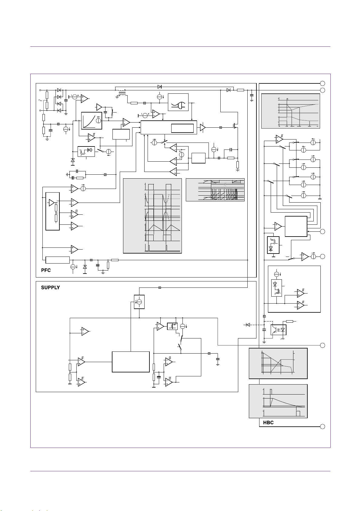
4. Application diagram and block diagrams
NXP Semiconductors
Fig 1. Basic application diagram TEA1713
TEA1713 resonant power supply control IC with PFC
AN10881
Page 13

NXP Semiconductors
coa073
1.2
MΩ
1.2
MΩ
1.2
MΩ
SNSMAINS
MainsReset
MainsUV
SoftStart
min
Ton
max
Ton
14
kΩ
9.8 MΩ
62 kΩ
3.3 μF
47 μA
60 μA
−39.....+39 μA
GmAmplifier
33 nA
800 mV
1 ×
5.8 V
2.5 V
120 μA
5.6 V
2.2 V
1.0 V
Enable
ENABLE DETECTION
EnablePfc
3.2 V
3.2 V
8.0 V
ClampEndSoftStart
40 μA
120 μA
40 μA
1360 μA
440 μA
5 μA
42 μA
FREQUENCY
CONTROL
HBC
D
C
B
A
E
F
33 nA
33 nA
R
SoStPfct
R
CurPfc
C
SoStPfct
45 nA
5.8 V
1 nF
2.5 V
0.4 V
Demag
ValleyPfc
DRIVE CONTROL
SPIKE
FILTER
0.1 V
0.5 V
0.52 V
50 mV
COMPPFC
SPIKE FILTER
BoostOv
BoostSCProt
BoostOv level = 2.63 V
BoostStart = 2.3 V
BoostUvp = 1.6 V
SNSBOOST
SUPHV
SNSAUXPFC
AuxPfc
SNSCURPFC
open pin
detection
PGND
SupReg
SSHBC/EN
Disable supply
Enable supply
0 to >2 V
GATEPFC
Boost
SUPREG
1.05 V
UV-Clamp
3.0 V
0.89 V
1.15 V
1.25 V
3.5 V
GatePfcDig
Ton
SoftStopEnd
OCPfc
I = c*V
2
8.4 V
demagnetized
V
Rect
/N
V
Rect
V
Boost
(V
Boost
− V
Rect
)/N
V
aux,demag
0
0
magnetized
Demagnetization
VALLEY SWITCHING
l
TrPfc
AuxPfc
DrPfc
GatePfc
Valley
(= top for detection)
0
off
on
t
VALLEY
DETECTION
frequency limit
125 kHz
SuplcChargeLow = 1.1 mA
SuplcCharge = 5.1 mA
HV START-UP SOURCE
CONTROL
0.65 V
10.9 V
5.4 mA
SUPIC
SupReg
EnableSupReg
reduced
current
SuplcShort
startlevel Hv = 22 V
startlevel Lv = 17 V
stoplevel = 15 V
SupRegUvStart
startlevel = 10.7 V
SupRegUvStop
stoplevel = 10.3 V
SupHvPresent
C
SUPREG
Protection
HBC softstart reset
0
V
fmax(SSHBC)
V
SSHBC/EN
V
fmin(SSHBC)
0
f
min
f
HB
f
max
t
off
on
f
max
forced
fast
sweep
slow sweep regulationregulation
V
ss(hf-lf)(SSHBC)
PFCsense
Iswitch
OCP_lvl
OCP_lvl
PFC driver
Start Rdy
0
0
0
0
0
Softstart, Softstop
Softstart Softstop
0
I
SNSFB
V
open
= 8.4 V
0.66 mA
I
fmin
V
RFMAX
2.2 mA
I
fmax
00
V
SSHBC
= 8 V
260 μA
I
OLP
V
OLP
= 7.7 V
V
fmin
= 6.4 V
V
fmax
= 4.1 V
V
clamp,fmax
= 3.2 V
V
SNSFB
8 mA
I
clamp,max
2.5 V
typ
= V
fmax
1.5 V
typ
= 0.6
× V
fmax
passed
0
no
yes
V
high(RCPROT)
V
low(RCPROT)
restart request
V
RCPROT
t
restart time
RESTART TIMER
014aaa864
001aal029
001aal040
001aal064
AN10881
TEA1713 resonant power supply control IC with PFC
Fig 2. Block diagram TEA1713
AN10881 All information provided in this document is subject to legal disclaimers. © NXP B.V. 2011. All rights reserved.
Application note Rev. 2 — 26 September 2011 13 of 102
Page 14
NXP Semiconductors
coa073
1.2
MΩ
1.2
MΩ
1.2
MΩ
SNSMAINS
MainsReset
MainsUV
SoftStart
min
Ton
max
Ton
14
kΩ
9.8 MΩ
62 kΩ
3.3 μF
47 μA
60 μA
−39.....+39 μA
GmAmplifier
33 nA
800 mV
1 ×
5.8 V
2.5 V
120 μA
5.6 V
2.2 V
1.0 V
Enable
ENABLE DETECTION
EnablePfc
3.2 V
3.2 V
8.0 V
ClampEndSoftStart
40 μA
120 μA
40 μA
1360 μA
440 μA
5 μA
42 μA
FREQUENCY
CONTROL
HBC
D
C
B
A
E
F
33 nA
33 nA
R
SoStPfct
R
CurPfc
C
SoStPfct
45 nA
5.8 V
1 nF
2.5 V
0.4 V
Demag
ValleyPfc
DRIVE CONTROL
SPIKE
FILTER
0.1 V
0.5 V
0.52 V
50 mV
COMPPFC
SPIKE FILTER
BoostOv
BoostSCProt
BoostOv level = 2.63 V
BoostStart = 2.3 V
BoostUvp = 1.6 V
SNSBOOST
SUPHV
SNSAUXPFC
AuxPfc
SNSCURPFC
open pin
detection
PGND
SupReg
SSHBC/EN
Disable supply
Enable supply
0 to >2 V
GATEPFC
Boost
SUPREG
1.05 V
UV-Clamp
3.0 V
0.89 V
1.15 V
1.25 V
3.5 V
GatePfcDig
Ton
SoftStopEnd
OCPfc
I = c*V
2
8.4 V
demagnetized
V
Rect
/N
V
Rect
V
Boost
(V
Boost
− V
Rect
)/N
V
aux,demag
0
0
magnetized
Demagnetization
VALLEY SWITCHING
l
TrPfc
AuxPfc
DrPfc
GatePfc
Valley
(= top for detection)
0
off
on
t
VALLEY
DETECTION
frequency limit
125 kHz
SuplcChargeLow = 1.1 mA
SuplcCharge = 5.1 mA
HV START-UP SOURCE
CONTROL
0.65 V
10.9 V
5.4 mA
SUPIC
SupReg
EnableSupReg
reduced
current
SuplcShort
startlevel Hv = 22 V
startlevel Lv = 17 V
stoplevel = 15 V
SupRegUvStart
startlevel = 10.7 V
SupRegUvStop
stoplevel = 10.3 V
SupHvPresent
C
SUPREG
Protection
HBC softstart reset
0
V
fmax(SSHBC)
V
SSHBC/EN
V
fmin(SSHBC)
0
f
min
f
HB
f
max
t
off
on
f
max
forced
fast
sweep
slow sweep regulationregulation
V
ss(hf-lf)(SSHBC)
PFCsense
Iswitch
OCP_lvl
OCP_lvl
PFC driver
Start Rdy
0
0
0
0
0
Softstart, Softstop
Softstart Softstop
0
I
SNSFB
V
open
= 8.4 V
0.66 mA
I
fmin
V
RFMAX
2.2 mA
I
fmax
00
V
SSHBC
= 8 V
260 μA
I
OLP
V
OLP
= 7.7 V
V
fmin
= 6.4 V
V
fmax
= 4.1 V
V
clamp,fmax
= 3.2 V
V
SNSFB
8 mA
I
clamp,max
2.5 V
typ
= V
fmax
1.5 V
typ
= 0.6
× V
fmax
passed
0
no
yes
V
high(RCPROT)
V
low(RCPROT)
restart request
V
RCPROT
t
restart time
RESTART TIMER
014aaa864
001aal029
001aal040
001aal064
AN10881
TEA1713 resonant power supply control IC with PFC
Fig 3. Block diagram TEA1713
AN10881 All information provided in this document is subject to legal disclaimers. © NXP B.V. 2011. All rights reserved.
Application note Rev. 2 — 26 September 2011 14 of 102
Page 15
coa076
1.5 kΩ
R
Prot
340 kΩ
C
Prot
640 nF
TEA1713 pin list:
1. COMPPFC
2. SNSMAINS
3. SNSAUXPFC
4. SNSCURPFC
5. SNSOUT
6. SUPIC
7. GATEPFC
8. PGND
9.SUPREG
10. GATELS
11. n.c.
12. SUPHV
24. SNSBOOST
23. RCPROT
22. SSHBC/EN
21. SNSFB
20. RFMAX
19. CFMIN
18. SGND
17. SNSCURHBC
16. n.c.
15. HB
14. SUPHS
13. GATEHS
Output
High
Voltage
Output
Low
Voltage
Output
Vout
CCO
RFMAX
FreqHigh
ProtTimer
30 μA
F
MAX,limit
R
fmax
C
fmin
FreqHbc
(75 % of max)
1.8 V
Slowed
down
current
CFMIN
V
high
= 3.0 V
V
low
= 1.0 V
HBC DRIVE CONTROL
Drive GateHS
Drive GateLS
Enable
Logic
SUPHS
GATEHS
Hb
HB
7.3 mA
3.2 V
6.4 V
2.2 mA
100 μA
100 μA
VOLTAGE PIN SSHBC
POLARITY INVERSION
(max 2.5 V)
VOLTAGE PIN RFMAX
HBC OSCILLATOR
CONVERSION TO CURRENT
via R
fmax
FEEDBACK CURRENT
PIN SNSFB
FIXED f
min
CURRENT
CONVERSION TO
VOLTAGE (max 1.5 V)
(DIS-)CHARGE CURRENT
PIN CFMIN
CONVERSION TO
FRQUENCY via C
fmin
V
Cur(HBC)
= R
cur(HBC)
× I
Cur(HBC)
I
ocr(high)
I
ocp(high)
I
ocp(nom)
I
ocr(nom)
−I
ocr(nom)
−I
ocp(nom)
−I
ocr(high)
−I
ocp(high)
I
Cur(HBC)
I
SNSCURHBC
HBC BOOST COMPENSATION
V
reg
V
uvp
V
Boost
GATELS
GATEHS
sink current only with positive V
SNSCURHBC
sink
source
0
0
0
t
t
t
t
low V
Boost
strong compensation
high OCP
low V
Boost
strong compensation
high OCR
nominal V
Boost
no compensation
nominal OCP
nominal V
Boost
no compensation
nominal OCR
V
SNSCURHBC
t
t
V
SNSCURHBC
V
ocr(HBC)
−V
ocr(HBC)
V
ocp(HBC)
−V
ocp(HBC)
0 μA
0 V 1.8 V
V
SNSBOOST
I
compensation on SNSCURHBC
2.5 V =
V
regulation
170 μA
−170 μA
500 mV
−500 mV
V
SNSCURHBC
160 μA
40 μA
−40 μA
−160 μA
I
SSHBC/EN
V
SSHBC/EN
8 V
5.6 V
3.2 V
V
Output
V
regulate
0
0
0
HBC 0CR
t
t
t
t
Fast soft-start sweep (charge and discharge) Slow soft-start sweep (charge and discharge)
ADAPTIVE NON OVERLAP
LEVEL
SHIFTER
Hb
SupHs
Drive GateHS
Drive GateLS
CAPACITIVE MODE REGULATION
fast HB slope
V
Boost
Hb
GateLs
GateHs
0
slow HB slope incomplete HB slope
t
f
HB,limit
f
max,B
V
fmax
V
RFMAX
A
curve C
fminRfmax
A high high
B low low
C low too low
B
C
f
max,A
f
min,
B and C
f
min,A
0
f
HB
SLOPE
DETECTION
SlopeNeg
SlopeNegStart
SlopePos
SlopePosStart
SupHs
SupHs
Hb
GATELS
SNSOUT
SNSFB
SupReg
1.5 V
3.5 V
2.35 V
1.1 V
0.4 V
ProtTimer
(latched)
ProtSd
OutputUv
OutputOv
HoldHbc
HoldPfc
RCPROT
Restart
Over Current Regulation HBC
High Frequency Protection HBC
Open Loop Protection SNSFB
Under Voltage Protection SNSOUT
Short Circuit Protection SNSBOOST (2.2 mA)
4.0 V
0.5 V
SNSCURHBC
SPIKE
FILTER
SUPIC
SupReg
PGND
HB
4.5 V
HB
SupReg
C
SupReg
C
Res2
C
CurHbc
C
Suplc
R
CurHbc
R
Curcmp
1 kΩ
C
Hb
C
Res1
SPIKE
FILTER
BOOST VOL TAGE
COMPENSATION
SnsBoost
2.5 V => 0 μA
1.7 V => 100 μA
1 V
1 V
0.5 V
0.5 V
0.4 V
8.1 V
8.4 V
ProtTimer
open loop level = 7.7 V
Freq.
Control
ProtTimer
Standby
(external)
supply
passed
0
0
none
present
short
error
long
error
PROTECTION TIMER
repetative
error
V
high(RCPROT)
I
slow(RCPROT)
I
RCPROT
Error
V
RCPROT
t
Protection time
Θ
RESTART/
PROTECTION TIMER CONTROL
014aaa865
014aaa860
001aal033
001aal037
001aal063
001aal044
B
C
D
E
F
A
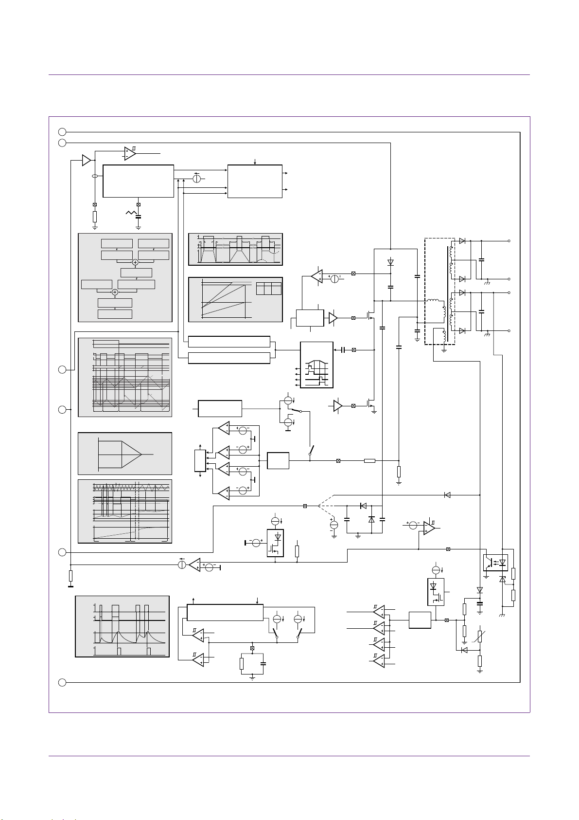
NXP Semiconductors
AN10881
TEA1713 resonant power supply control IC with PFC
Fig 4. Block diagram TEA1713
AN10881 All information provided in this document is subject to legal disclaimers. © NXP B.V. 2011. All rights reserved.
Application note Rev. 2 — 26 September 2011 15 of 102
Page 16

NXP Semiconductors
001aal017
TEA1713
MAINS
VOLT AGE
12
SUPHV
22 V
start when HVsupply
enable HVsource
start when LVsupply
stop, UVP
shutdown reset
COMP
0.65 V
COMP
17 V
COMP
7 V
COMP
15 V
COMP
start
EXTERNAL
stop
10.7 V
10.9 V
COMP
GATEPFC
GATEHS
14
15
9
SUPHS
HB
SUPREG
6 SUPIC
V
AUXILIARY
5 SNSOUT
GATELS
10.3 V
COMP
OVP
latched
shutdown
UVP
protection
timer
3.5 V
COMP
2.35 V
COMP
1.1 mA5.1 mA
HV
STARTUP
CONTROL
V
BOOST
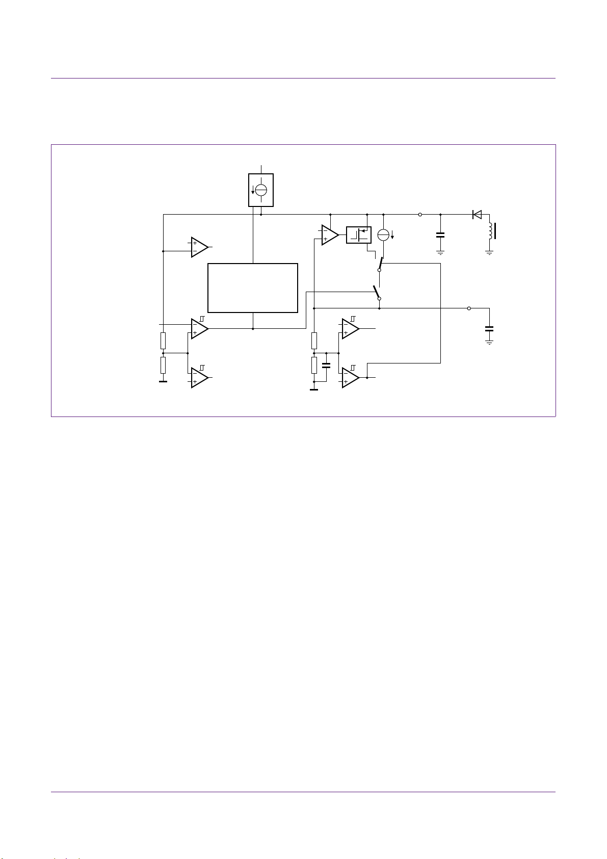
5. Supply functions
5.1 Basic supply system overview
AN10881
TEA1713 resonant power supply control IC with PFC
Fig 5. Basic overview internal IC supplies
5.1.1 TEA1713 supplies
The main supply for the TEA1713 is SUPIC.
SUPHV can be used to charge SUPIC for starting the supply. During operation a supply
voltage is applied to SUPIC and the SUPHV source is switched off. The SUPHV source is
only switched on again at a new start-up.
The internal regulator SUPREG generates a fixed voltage of 10.9 V to supply the internal
AN10881 All information provided in this document is subject to legal disclaimers. © NXP B.V. 2011. All rights reserved.
Application note Rev. 2 — 26 September 2011 16 of 102
MOSFET drivers: GATEPFC, GATELS and GATEHS. A bootstrap function with an
external diode is used to make supply SUPHS.This is used to supply GATEHS.
SUPIC and SUPREG also supply other internal TEA1713 circuits.
Page 17

NXP Semiconductors
5.1.2 Supply monitoring and protection
The supply voltages are internally monitored to determine when to initiate certain actions,
such as starting, stopping or protection.
In several applications (e.g. when using an auxiliary winding construction) the SUPIC
voltage can also be used to monitor the HBC output voltage by protection input SNSOUT.
5.2 SUPIC - the low voltage IC supply
SUPIC is the main IC supply. Except for the SUPHV circuit, all internal circuits are either
directly or indirectly supplied from this pin.
5.2.1 SUPIC start-up
Connect SUPIC to an external buffer capacitor. This buffer capacitor can be charged in
several ways:
• Internal high-voltage (HV) start-up source
• Auxiliary supply , e.g. from a winding on the HBC transformer
• External DC supply, e.g. from a standby supply
AN10881
TEA1713 resonant power supply control IC with PFC
The IC starts operating when the SUPIC and SUPREG voltage have reached the start
level. The start level value of SUPIC depends on the condition of the SUPHV pin.
5.2.1.1 SUPHV 25 V
This is the case in a standalone application where the HV start-up source initially charges
SUPIC. The SUPIC start level is 22 V. The large difference between start level and stop
level (15 V) is used to allow discharge of the SUPIC capacitor until the auxiliary supply
can take over the IC supply.
5.2.1.2 SUPHV not connected/used
This is the case when the TEA1713 is supplied from an external DC supply. The SUPIC
start level is now 17 V. During start-up and operation the IC is continuously supplied by
the external DC supply. The SUPHV pin must not be connected for this kind of application.
max
5.2.2 SUPIC stop, UVP and SCP
The IC stops operating when the SUPIC voltage drops below 15 V which is the
UnderVoltage Protection (UVP) of SUPIC. While in the process of stopping, the HBC
continues until the low-side MOSFET is active, before stopping the PFC and HBC
operation.
SUPIC has a low level detection at 0.65 V to detect a short circuit to ground. This level
also controls the current source from the SUPHV pin.
AN10881 All information provided in this document is subject to legal disclaimers. © NXP B.V. 2011. All rights reserved.
Application note Rev. 2 — 26 September 2011 17 of 102
Page 18

NXP Semiconductors
5.2.3 SUPIC current consumption
The SUPIC current consumption depends on the state of the TEA1713.
• Disabled IC state:
• SUPIC charge, SUPREG charge, thermal hold, restart and shutdown state:
• Boost charge state:
• Operating supply state:
AN10881
TEA1713 resonant power supply control IC with PFC
When the IC is disabled via the SSHBC/EN pin, the current consumption is low at
250 A.
During the charging of SUPIC and SUPREG before start-up, during a restart
sequence or during shutdown after activation of protection, only a small part of the IC
is active. The PFC and HBC are disabled. The current consumption from SUPIC in
these states is small at 400 A.
PFC is switching and HBC is still off. The current from the high-voltage start-up source
is large enough to supply SUPIC, so current consumption is below the maximum
current (5.1 mA) that SUPHV can de live r.
Both PFC and HBC are switching. The current consumption is larger. The MOSFET
drivers are dominant in the current consumption (see Section 5.5.5
soft-start of the HBC, when the switching frequency is high, and also during normal
operation. Initially, the stored energy in the SUPIC capacitor delivers the SUPIC
current. After a short time the current supply is taken over by the supply source on
SUPIC during normal operation.
), especially during
5.3 SUPIC supply using HBC transformer auxiliary winding
5.3.1 Start-up by SUPHV
In a standalone power supply application, the IC can be started by a high-voltage source
such as the rectified mains voltage by connecting the high-voltage input SUPHV to the
boost voltage (PFC output voltage).
The internal HV start-up source, which delivers a const ant current from SUPHV to SUPIC,
charges the SUPIC and SUPREG. SUPHV is operational at a voltage > 25 V.
As long as the voltage at SUPIC is below the short circuit protection level (0.65 V), the
current from SUPHV is low (1.1 mA). This is to limit the dissipation in the HV start-up
source when SUPIC is shorted to ground.
During normal conditions, SUPIC quickly exceeds the protection level and the HV st art-up
source switches to normal current (5.1 mA). The HV start-up source switches off when
SUPIC has reached the start level (22 V). The current consumption from SUPHV is low
(7 A) when switched off.
When SUPIC has reached the start level (22 V), SUPREG is charged. When SUPREG
reaches the level of 10.7 V, it enables operation of HBC and PFC.
The auxiliary winding supply of the HBC transformer must take over the supply of SUPIC
before it is discharged to the SUPIC under voltage stop level (15 V).
AN10881 All information provided in this document is subject to legal disclaimers. © NXP B.V. 2011. All rights reserved.
Application note Rev. 2 — 26 September 2011 18 of 102
Page 19
NXP Semiconductors
001aal018
SuplcChargeLow = 1.1 mA
SuplcCharge = 5.1 mA
SuplcCharge = off
HV START-UP SOURCE
CONTROL
0.65 V
10.9 V
5.5 mA
SUPIC
SUPHV
SUPREGSupReg
EnableSupReg
V
AUXILIARY
reduced
current
SuplcShort
startlevel Hv = 22 V
startlevel Lv = 17 V
stoplevel = 15 V
SupRegUvStart
startlevel = 10.7 V
SupRegUvStop
stoplevel = 10.3 V
SupHvPresent
C
SUPREG
5.3.2 Block diagram for SUPIC start-up
AN10881
TEA1713 resonant power supply control IC with PFC
Fig 6. Block diagram: SUPIC and SUPREG start-up with SUPHV and auxiliary supply
5.3.3 Auxiliary winding on the HBC transformer
An auxiliary winding on the HBC transformer can be used to obtain a supply voltage for
SUPIC during operation. As SUPIC has a wide operational voltage range (15 V to 38 V),
this is not a critical parameter.
But:
• The voltage on SUPIC must be low for low power consumption.
• The auxiliary supply must be made accurately representing the output voltage to use
the voltage from the auxiliary winding for IC supply and HBC output voltage
measurement (by SNSOUT). Place this winding on the secondary (output) side to
ensure good coupling.
• When mains insulation is included in the HBC transformer, it can impact the
construction of the auxiliary winding. Triple insulated wire is needed when the
auxiliary winding is placed on the mains-insulated area of the transformer
construction.
AN10881 All information provided in this document is subject to legal disclaimers. © NXP B.V. 2011. All rights reserved.
Application note Rev. 2 — 26 September 2011 19 of 102
Page 20

NXP Semiconductors
001aal019
Fig 7. Auxiliary winding on primary side (left) and secondary side (right)
5.3.3.1 SUPIC and SNSOUT by auxiliary winding
The SNSOUT input provides a combination of four functions:
• Overvoltage protection: SNSOUT > 3.5 V, latched
• Undervoltage protection: SNSOUT < 2.35 V, protection timer
• Hold HBC: SNSOUT < 1.1 V, stop switching HBC (for Burst mode)
• Hold HBC + PFC: SNSOUT < 0.4 V, stop switching HBC and PFC (for Burst mode)
AN10881
TEA1713 resonant power supply control IC with PFC
Remark: A more detailed explanation of the SNSOUT functions can be found in
Section 10.3.1
Often, a circuit is used which combines SUPIC and the output voltage monitoring by
SNSOUT, with one auxiliary winding on the HBC transformer. But an independent
construction for SUPIC and SNSOUT is also possible. This could be in a situation where
SUPIC is supplied by a separate standby supply and an auxiliary winding is only used for
output voltage sensing. It is also possible not to use SNSOUT for output sensing but as a
general-purpose protection input. See Section 10.3.3
In a combined function of SUPIC and SNSOUT by an auxiliary winding on the HBC
transformer, some issues must be addressed to obtain a good representation of the output
voltage for SNSOUT measurement.
The advantage of a good coupling/representation of the auxiliary winding with the output
windings is also that a stable auxiliary voltage is obtained for SUPIC. A low SUPIC voltage
value can be designed more easily for lowest power consumption.
5.3.3.2 Auxiliary supply voltage variations by output current
At high (peak) current loads, the voltage drop across the series components of the HBC
output stage (resistance and diodes) is compensated by regulation. This results in a
higher voltage on the windings at higher output currents due to the higher currents
causing a larger voltage drop across the series components. An auxiliary winding supply
shows this variation caused by the HBC output.
and Section 10.3.2.
for more information.
5.3.3.3 Voltage variations by auxiliary winding position: primary side component
Due to a less optimal position of the auxiliary winding, the voltage for SNSOUT and/or
SUPIC can contain a certain amount of undesired primary voltage component. This can
seriously endanger the feasibility of the SNSOUT sensing function.
AN10881 All information provided in this document is subject to legal disclaimers. © NXP B.V. 2011. All rights reserved.
Application note Rev. 2 — 26 September 2011 20 of 102
Page 21
NXP Semiconductors
001aal020
secondary side
primary side
V
aux
V
aux
V
aux.new
V
aux.new
V
O
V
O
V
O
Bad coupling V
aux
to VO at high
output current
Good coupling
V
aux.new
to VO at
high output current
The coupling of the auxiliary winding with the primary winding must be as small as
possible to avoid a primary voltage component on the auxiliary voltage. Place the auxiliary
winding on the secondary winding(s) and as physically remote as possible from the
primary winding to obtain this. See differences in results given by comparison on
secondary side position in Figure 8
AN10881
TEA1713 resonant power supply control IC with PFC
.
Fig 8. Position the auxiliary winding for good output coupling
5.3.4 Difference between UVP on SNSOUT and SNSCURHBC OCP/OCR
In a system that uses output voltage sensing with the SNSOUT function, there can be an
overlap in functionality in an over power or short-circuit situation. In such a situation, often
both the SNSOUT UVP and the OCP/OCR on SNSCURHBC, activate the protection
timer.
There are basic differences between both functions:
• SNSOUT monitors (indirectly) the HBC output voltage or another external protection
circuit (such as NTC temperature measurement)
• OCP/OCR monitors the power in the system by sensing the primary current in detail
SNSOUT is a more general usable protection input while SNSCURHBC is specifically
designed for HBC operation. In addition, SNSOUT also of fers three other functions:
• OVP (latched)
• hold HBC
• hold HBC + PFC (for Burst mode)
AN10881 All information provided in this document is subject to legal disclaimers. © NXP B.V. 2011. All rights reserved.
Application note Rev. 2 — 26 September 2011 21 of 102
Page 22

NXP Semiconductors
5.4 SUPIC supply by external voltage
5.4.1 Start-up
When the TEA1713 is supplied by an external DC supply, the SUPHV pin can remain
unconnected. The SUPIC start level is now 17 V.
When the SUPIC exceeds 17 V the internal regulator is activated and charge SUPREG.
At SUPREG 10.7 V, GATELS is switched on for the bootstrap function to charge
SUPHS. And at the same time the PFC operation is internally enabled. When all enable
conditions are met, the TEA1713 starts the PFC function and when V
approximately 90 % (SNSBOOST 2.3 V) of its nominal value, the HBC starts.
5.4.2 Stop
Operation of the TEA1713 can be stopped by switching off the external source for SUPIC.
When the voltage level on SUPIC drops below 15 V, operation is stopped.
In case of shutdown (because of protection), this state is reset by internal logic when the
SUPIC voltage drops below 7 V.
AN10881
TEA1713 resonant power supply control IC with PFC
reaches
boost
5.5 SUPREG
SUPIC has a wide voltage range for easy application. Because of this, SUPIC cannot be
directly used to supply the internal MOSFET drivers as this would exceed the allowed
gate voltage of many external MOSFETs.
The TEA1713 contains an integrated series stabilizer to avoid this issue and to create a
few other benefits. The series stabilizer generates an accurate regulated voltage on
SUPREG on the external buffer capacitor.
This stabilized SUPREG voltage is used for:
• Supply of internal PFC driver
• Supply of internal low-side HBC driver
• Supply of internal high-side driver via external components
• Reference voltage for optional external circuits
The series stabilizer for SUPREG is enabled after SUPIC has been charged. In this way
optional external circuitry at SUPREG does not consume from the start-up current during
the charging of SUPIC. The capacitor on SUPIC acts as a buffer at charge of SUPREG
and start-up of the IC.
The SUPREG voltage must reach the V
ensure that the external MOSFETs receive sufficient gate drive, provided that the SUPIC
voltage has also reached the start level.
start(SUPREG)
level before the IC starts operating to
AN10881 All information provided in this document is subject to legal disclaimers. © NXP B.V. 2011. All rights reserved.
Application note Rev. 2 — 26 September 2011 22 of 102
Page 23
NXP Semiconductors
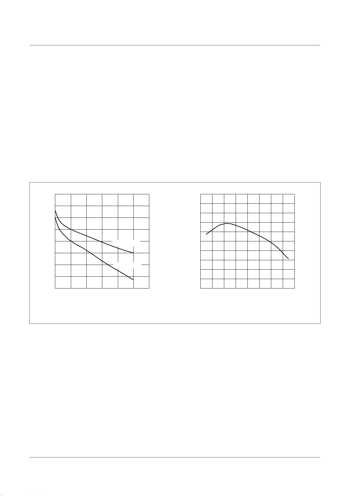
001aal002
SUPREG load current (mA)
0604020
10.905
10.895
10.915
10.925
SUPREG
voltage
(V)
10.885
SUPIC = 17 V
SUPIC = 20 V
Temperature (°C)
−50 150100050
001aal021
10.85
10.90
10.80
10.95
11.00
SUPREG
voltage
(V)
10.75
The SUPREG has an UnderVoltage Protection. When the SUPREG voltage drops below
the 10.3 V two actions take place:
• The IC stops operating to prevent unreliable switching due to too low gate driver
• The maximum current from the internal SUPREG series stabilizer is reduced to
It is important to realize that in principle, SUPREG can only source current.
The drivers of GATELS and GATEPFC are supplied by this volt age and dr aw current fr om
it during operation depending on the operating condition. Some change in value can be
expected due to current load and temperature:
AN10881
TEA1713 resonant power supply control IC with PFC
voltage. The PFC controller stops switching immediately, but the HBC continues until
the low-side stroke is active.
5.4 mA. In case of an overload at SUPREG in combination with an external DC supply
for SUPIC, this action reduces the dissipation in the series stabilizer.
Voltage characteristics for load Voltage characteristics for temperature
Fig 9. Typical SUPREG voltage characteristics for load and temperature
AN10881 All information provided in this document is subject to legal disclaimers. © NXP B.V. 2011. All rights reserved.
Application note Rev. 2 — 26 September 2011 23 of 102
Page 24
NXP Semiconductors
001aal022
11 V
5.4 mA
C
SUPIC
C
SUPREG
SUPIC
SUPREGSupReg
EnableSupReg
SUPHV SOURCE
V
AUXILIARY
reduced
current
SupRegUvStart
startlevel = 10.7 V
SupRegUvStop
stoplevel = 10.3 V
001aal023
EXTERNAL
GATE CIRCUIT
SUPREG
R
DS-ON
Cgs
Vgs
I
discharge
I
charge
R
DS-ON
TEA1713
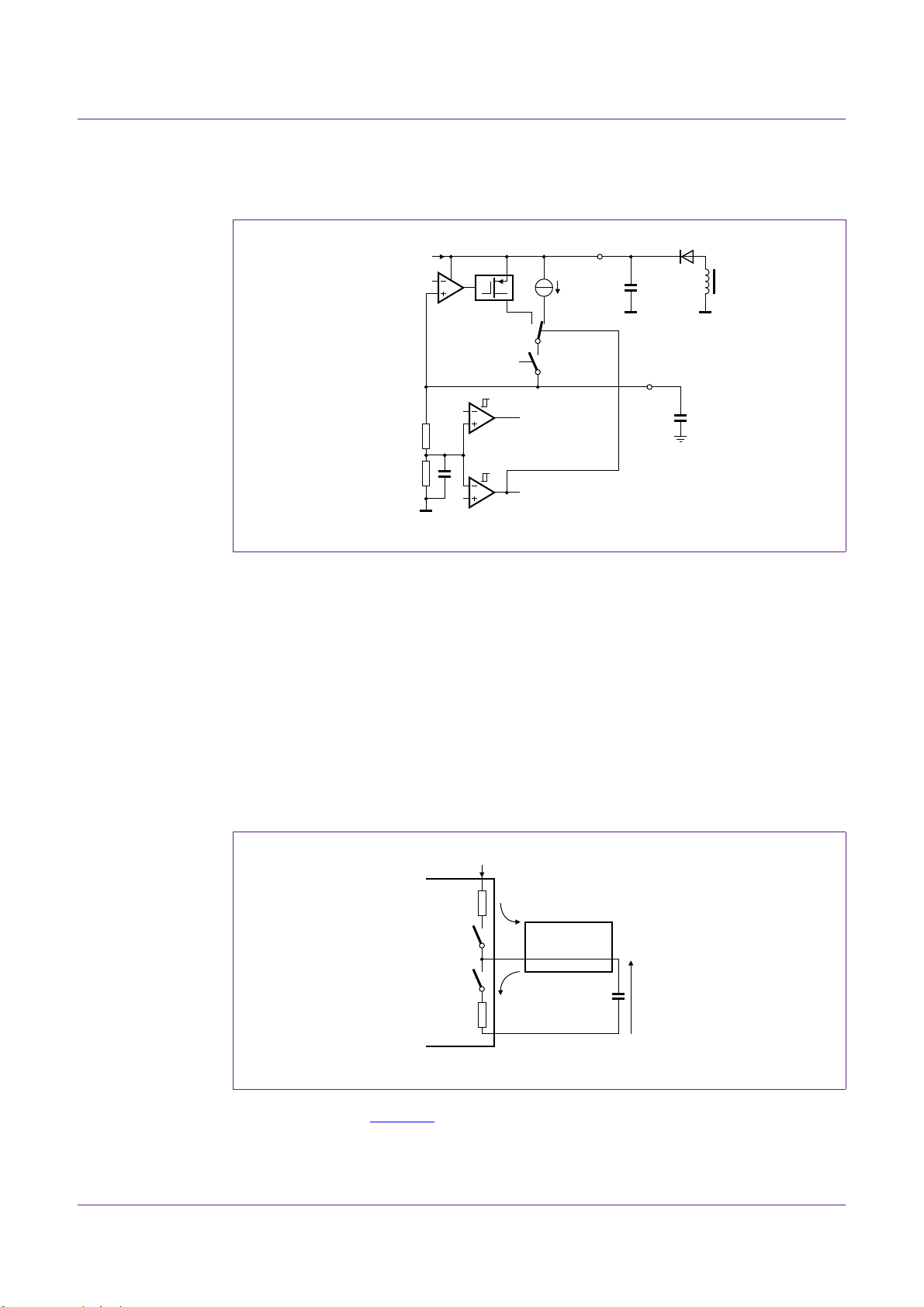
5.5.1 Block diagram of SUPREG regulator
Fig 10. Block diagram of internal SUPREG regulator
AN10881
TEA1713 resonant power supply control IC with PFC
5.5.2 SUPREG during start-up
SUPREG is supplied by SUPIC. SUPIC is the unregulated external powe r sou rc e th at
provides the input voltage for the internal voltage regulator that provides SUPREG.
At start-up SUPIC must reach a specific voltage level before SUPREG is activated:
• Using the internal HV supply, SUPREG is activated when SUPIC 22 V
• Using an external low voltage supply, SUPREG is activated when SUPIC 17 V
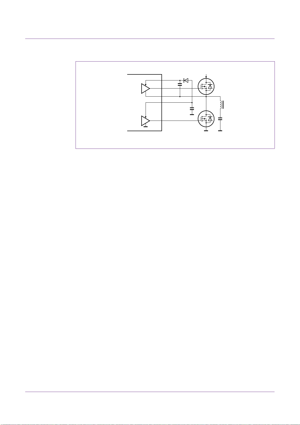
5.5.3 Supply voltage for the output drivers: SUPREG
The TEA1713 has a powerful output stage for GATEPFC and GATELS to drive large
MOSFETs. These internal drivers are supplied by SUPREG that provides a fixed voltage.
Fig 11. Simplified model of MOSFET drive
It can be seen from Figure 11 that current is taken from SUPREG when the external
MOSFET is switched on by charging the gate to a high voltage.
AN10881 All information provided in this document is subject to legal disclaimers. © NXP B.V. 2011. All rights reserved.
Application note Rev. 2 — 26 September 2011 24 of 102
Page 25

NXP Semiconductors
The shape of the current from SUPREG at switch-on is related to:
• The supply voltage for the internal driver (10.9 V)
• The characteristic of the internal driver
• The gate capacitance to be charge d
• The gate threshold voltage for the MOSFET to switch on
• The external circuit to the gate
Remark: The switching moments of GATEPFC and GATELS are independent in time.
The charging of SUPHS for GATEHS is synchronized in time with GATELS but has a
different shape because of the bootstrap function.
5.5.4 Supply voltage for the output drivers: SUPHS
The high-side driver is supplied by an external bootstrap buffer capacitor. The bootstrap
capacitor is connected between the high-side reference pin HB and the high-side driver
supply input pin SUPHS. During the time that HB is low an external diode from SUPREG
charges this capacitor. By selecting a suitable external diode, the voltage drop between
SUPREG and SUPHS can be minimized. This is especially important when using a
MOSFET that needs a large amount of gate charge and/or when switching at high
frequencies.
AN10881
TEA1713 resonant power supply control IC with PFC
Instead of using SUPREG as the power source for charging SUPHS, another supply
source can be used. In such a construction it is important to check for correct start/stop
sequences and to prevent the voltage exceeding the maximum value of HB +14 V.
Remark: The current taken from SUPREG to charge SUPHS differs for each cycle in time
and shape from the current taken by drivers GATEPFC and GATELS.
5.5.4.1 Initial charging of SUPHS
At start-up, SUPHS is charged by the bootstrap function by setting GATELS high to switch
on the low side MOSFET. While SUPHS is being charged, GATELS is switched on for
charging and the PFC operation is started. The time betwe en start charging and start HBC
operation is normally sufficient to charge SUPHS completely. Start HBC operation is when
SNSBOOST reaches 2.3 V which is approximately 90 % of the nominal V
5.5.4.2 Current load on SUPHS
The current taken from SUPHS consists of two parts:
• Internal MOSFET driver GATEHS
• Internal circuit to control GATEHS (37 A, quiescent current)
Figure 12
shape of the current from SUPHS at switch-on is related to:
shows that the current taken by the driver GATEHS occurs at switch-on. The
• The value of the supply voltage for the internal driver
• The characteristic of the internal driver
• The gate capacitance to be charge d
• The gate threshold voltage for the MOSFET to switch on
• The external circuit to the gate
boost
.
The voltage value of SUPHS can vary.
AN10881 All information provided in this document is subject to legal disclaimers. © NXP B.V. 2011. All rights reserved.
Application note Rev. 2 — 26 September 2011 25 of 102
Page 26
NXP Semiconductors
001aal024
14 SUPHS
GATEHS
GATELS
15 HB
9 SUPREG
V
BOOST
TEA1713
I
SUPIC
2Q
gatefbridge
=
Fig 12. Typical application of SUPHS
5.5.4.3 Lower voltage on SUPHS
During normal operation, each time the Half-Bridge (HB) node is switched to grou nd level,
the bootstrap function charges the SUPHS capacitor. Because of the voltage drop across
the bootstrap diode, the value of SUPHS is normally lower than SUPREG (or other
bootstrap supply input).
AN10881
TEA1713 resonant power supply control IC with PFC
The voltage drop across the bootstrap diode is directly related to the am ount of current
that is required to charge SUPHS. The resultant SUPHS voltage also has a relation to the
time available for charging.
A large voltage drop occurs when an externa l MOSFET with a large gate capacit ance has
to be switched at high frequency (high current and a short time).
Also, during Burst mode operation, a low voltage on SUPHS can occur. In Burst mode
there are (long) periods of not switching and therefore no ch arging of SUPHS. Dur ing th is
time the circuit supplied by SUPHS slowly discharges the supply volt age cap a citor. When
a new burst starts, the SUPHS voltage is lower than during normal operation. During the
first switching cycles SUPHS is recharged to its normal level. During Burst mode, at low
output power , the switching frequency is normally rather high which limits a fast recovery
of the SUPHS voltage.
Although in most applications the voltage drop is limited, it is an important issue to be
evaluated. It can influence the selection of the best diode type for the bootstrap function
and the value of the buffer capacitor on SUPHS.
5.5.5 SUPREG power consumed by MOSFET drivers
During operation the drivers GATEPFC, GATELS and GATEHS charging the gate
capacitances of the external MOSFETs are a major part of the power consumption from
SUPREG. The amount of energy required in time is linear to the switching frequency.
Often, for the MOSFETs used, the total charge is specified for certain conditions. With this
figure an estimation can be made for the amount of current needed from SUPREG.
5.5.5.1 GATELS and GATEHS (driving a total of two MOSFETs)
AN10881 All information provided in this document is subject to legal disclaimers. © NXP B.V. 2011. All rights reserved.
Application note Rev. 2 — 26 September 2011 26 of 102
(1)
Page 27

NXP Semiconductors
I
SUPIC
240 nC 100 kHz 8 mA==
I
SUPIC
Q
gatefPFC
=
I
SUPIC
40 nC 100 kHz 4 mA==
Example:
AN10881
TEA1713 resonant power supply control IC with PFC
• Q
• f
gate
bridge
=40nC
=100kHz
Remark: The calculated value is generally higher than the practical value, because the
switching operation deviates from the MOSFET specification for Q
5.5.5.2 GATEPFC
Example:
• Q
• f
gate
bridge
=40nC
=100kHz
5.5.6 SUPREG supply voltage for other circuits
The regulated voltage of SUPREG can also be used as a regulated supply for an external
circuit. The load of the external circuits affects the start-up (time) and the total load
(IC + extern al circ uit ) of SUPREG durin g op e ra tio n.
gate
.
(2)
5.5.6.1 Current available for supplying an external circuit from SUPREG
The total current available from SUPREG is a minimum of 40 mA. How much current the
IC is using must be determined to ensure how much current is available for an external
circuit.
I
SUPREG_for_external
=40mA I
SUPREG_for_IC
With respect to the IC, by far the greatest amount of current from SUPREG is consumed
by the MOSFET drivers (GATELS, GA TEHS and GATEPFC). Other circuit pa rt s in the IC,
consume a maximum of 3 mA.
I
SUPREG_for_IC=ISUPREG_for_MOSFET-drivers+ISUPREG_for_other_IC-circuits
I
SUPREG_for_IC=ISUPREG_for_MOSFET-drivers
I
SUPREG_for_MOSFET-drivers
can be estimated by the method provided in Section 12
+4mA
max
5.5.6.2 An estimation by measurement
The current used by SUPIC, while supplying the circuit from an external power supply , can
be assumed as a first approximation of how much current the IC circuits take from
SUPREG. Using this value, an estimation can be made of the power available for external
circuits.
Remark: The highest power consumption value is reached when the MOSFET drivers
are switching at the highest frequency.
AN10881 All information provided in this document is subject to legal disclaimers. © NXP B.V. 2011. All rights reserved.
Application note Rev. 2 — 26 September 2011 27 of 102
Page 28

NXP Semiconductors
C
SUPICISUPIC start-up
t
Vaux 15 V
V
SUPIC start-up
----------------------------------------- -
10 mA
70 ms
7 V
-------------- -
100 F==
Example:
AN10881
TEA1713 resonant power supply control IC with PFC
I
SUPIC(maximum measured)
I
SUPREG(for IC circuits)=ISUPIC(maximum measured)
I
SUPREG(for externals)
=18mA
=40mA I
=18mA
SUPREG(for IC circuits)
=40mA 18 mA = 22 mA
Remark: SUPREG must remain above the undervoltage protection level of 10.3 V to
maintain full functionality. During start-up, high external current loads can lead to
problems.
5.6 Value of the capacitors on SUPIC, SUPREG and SUPHS
Some practical examples are provided in Section 12.
5.6.1 Value of the capacitor on SUPIC
5.6.1.1 General
Use two types of capacitors on SUPIC. An SMD ceramic type with a smaller value located
close to the IC and an electrolytic type with the major part of the capacitance.
5.6.1.2 Start-up
When the supply is initially provided by an HV source, before being handled by an
auxiliary winding, a larger capacitor is needed. The capacitor value must be large enough
to handle the start-up before the auxiliary winding takes over the supply of SUPIC.
Example:
• I
SUPIC(start-up)
• V
SUPIC(start-up)
• t
Vaux>15V
=10mA
=22V 15 V = 7 V
=70ms
5.6.1.3 Normal operation
The main purpose of the capacitors on SUPIC for normal operation is to keep the current
load variations (e.g. gate drive currents) local.
5.6.1.4 Burst mode operation
When Burst mode operation is applied, the supply construction often uses an auxiliary
winding and start-up from an HV source. While in Burst mode there is a long period during
which the auxiliary winding is not able to charge the SUPIC because there is no HBC
switching (time between two bursts). Therefore, the capacitor value on SUPIC must be
large enough to keep the voltage above 15 V to prevent activating the SUPIC
undervoltage stop level.
(3)
AN10881 All information provided in this document is subject to legal disclaimers. © NXP B.V. 2011. All rights reserved.
Application note Rev. 2 — 26 September 2011 28 of 102
Page 29

NXP Semiconductors
C
SUPICISUPIC start-up between 2 bursts
t
between 2 bursts
V
SUPIC burst
---------------------------------------- -
4 mA
25 ms
4 V
-------------- -
25 F==
Example:
AN10881
TEA1713 resonant power supply control IC with PFC
• I
SUPIC(between 2 bursts)
• V
SUPIC(burst)=Vaux burst
• t
between 2 bursts
=4mA
15 V = 19 V 15 V = 4 V
=25ms
5.6.2 Value of the capacitor for SUPREG
The capacitor on SUPREG must not be larger than the capacitor on SUPIC to support
charging of SUPREG during an HV source start. This is to prevent a severe voltage drop
on SUPIC due to the charge of SUPREG. If SUPIC is supplied by an external (standby)
source, this is not important.
SUPREG is the supply for the current of the gate drivers. Keepin g current peaks lo cal can
be achieved using an SMD ceramic capacitor supported by an electrolytic capacitor. This
is necessary to provide sufficient capacitance to prevent voltage drop during high current
loads. The value of the capacitor on SUPREG must be much larger than the (total)
capacitance of the MOSFETs that must be driven (including the SUPHS parallel load and
capacitor bootstrap construction) to prevent significant voltage drop.
When considering the internal voltage regu lator , the value of the cap acitance on SUPREG
must be 1 F. Often a much larger value is used for the reasons mentioned previously.
(4)
5.6.3 Value of the capacitor for SUPHS
The SUPHS capacitor must be much larger than the gate capacitance to support charging
the gate of the high side MOSFET. This is to prevent a significant voltage drop on SUPHS
by the gate charge. When Burst mode is applied, SUPHS is discharged by 37 A during
the time between two bursts.
AN10881 All information provided in this document is subject to legal disclaimers. © NXP B.V. 2011. All rights reserved.
Application note Rev. 2 — 26 September 2011 29 of 102
Page 30
NXP Semiconductors
001aal024
14 SUPHS
GATEHS
GATELS
15 HB
9 SUPREG
V
BOOST
TEA1713
TEA1713 resonant power supply control IC with PFC
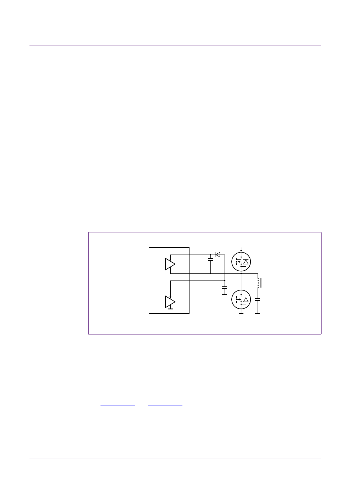
6. MOSFET drivers GATEPFC, GATELS and GATEHS
The TEA1713 provides three outputs for driving external high- voltage power MOSFETs:
• GATEPFC for driving the PFC MOSFET
• GATELS for driving the low side of the HBC MOSFET
• GATEHS for driving the low side of the HBC MOSFET
6.1 GATEPFC
The TEA1713 has a strong output stage for PFC to drive a high-voltage power MOSFET.
It is supplied by the fixed voltage from SUPREG = 10.9 V.
6.2 GATELS and GATEHS
Both drivers have identical driving capabilities for the gate of an external high-voltage
power MOSFET. The low-side driver is referenced to pin PGND and is supplied from
SUPREG. The high-side driver is floating, referenced to HB, the connection to the
midpoint of the external half-bridge. The high-side driver is supplie d by a capacitor on
SUPHS that is supplied by an external bootstrap function by SUPREG. The bootstrap
diode charges the capacitor on SUPHS when the low-side MOSFET is on.
AN10881
Fig 13. GATELS and GATEHS drivers
Both HBC drivers have a strong current source capability and an extra strong current sink
capability. In general operation of the HBC, fast switch-on of the external MOSFET is not
critical, as the HB node swings automatically to the correct state after switch-off. Fast
switch off however, is important to limit switching losses and prevent delay especially at
high frequency.
6.3 Supply voltage and power consumption
See Section 5.5.3 and Section 5.5.5.for a description of the supply voltages and power
consumption by the MOSFET drivers.
AN10881 All information provided in this document is subject to legal disclaimers. © NXP B.V. 2011. All rights reserved.
Application note Rev. 2 — 26 September 2011 30 of 102
Page 31

NXP Semiconductors
001aal025
GATEPFC
GATEPFC
GATEPFC
GATEPFC
d.
c.
b.
a.
6.4 General subjects on MOSFET drivers
6.4.1 Switch on
The time to switch on depends on:
• The supply voltage for the internal driver
• The characteristic of the internal driver
• The gate capacitance to be charge d
• The gate threshold voltage for the MOSFET to switch on
• The external circuit to the gate
6.4.2 Switch off
The time to switch off depends on:
• The characteristic of the internal driver
• The gate capacitance to be discharged
• The voltage on the gate just before discharge
• The gate threshold voltage for the MOSFET to switch off
• The external circuit to the gate
AN10881
TEA1713 resonant power supply control IC with PFC
Because the timing for switching off the MOSFET is more critical than switching it on, the
internal driver can sink more current than it can source . At higher frequencies and/or short
on-time, timing becomes more critical for correct switching. Sometimes a compromise
must be made between fast switching and EMI effects. A gate circuit between the driver
output and the gate can be used to optimize the switching behavior.
Fig 14. Gate circuits examples
Switching the MOSFETs on and off by the drivers can be approximated by alternating
charge and discharge of a (gate-source) capacitance of the MOSFET through a resistor
(R
of the internal driver MOSFET).
DSon
AN10881 All information provided in this document is subject to legal disclaimers. © NXP B.V. 2011. All rights reserved.
Application note Rev. 2 — 26 September 2011 31 of 102
Page 32

NXP Semiconductors
001aal023
EXTERNAL
GATE CIRCUIT
SUPREG
R
DS-ON
Cgs
Vgs
I
discharge
I
charge
R
DS-ON
TEA1713
Fig 15. Simplified model of a MOSFET drive
6.5 Specifications
The main function of the internal MOSFET drivers is to source current and sink current to
switch the external MOSFET switch on and off.
AN10881
TEA1713 resonant power supply control IC with PFC
The amount of current that can be sunk and sourced is specified to show the capability of
the internal driver.
The simplified model in Figure 15
demonstrates that the values of the charge current and
discharge current are strongly dependant upon the conditions of the supply voltage and
gate voltage. The value of the source current is highest when the supply voltage is highest
and the gate voltage 0 V. The value of the sink- current is h ighest when the gate voltage is
highest.
Table 3. PFC and HBC driver specifications
Symbol Parameter Conditions Min Typ Max Unit
PFC driver (pin GATEPFC)
I
source(GATEPFC)
I
sink(GATEPFC)
HBC high-side and low-side driver (pins GATEHS and GATELS)
I
source(GATEHS)
I
source(GATELS)
I
sink(GATEHS)
I
sink(GATELS)
source current on pin GATEPFC V
sink current on pin GATEPFC V
source current on pin GATEHS V
source current on pin GATELS V
sink current on pin GATEHS V
sink current on pin GATELS V
GATEPFC
GATEPFC
V
GATEPFC
GATEHS
GATELS
GATEHS
V
GATEHS
GATELS
V
GATELS
=2V - 0.5 - A
=2V - 0.7 - A
=10V - 1.2 - A
VHB=4V - 310 - mA
V
=4V - 310 - mA
PGND
VHB=2V - 560 - mA
VHB=11V - 1.9 - A
V
V
=2V - 560 - mA
PGND
=11V - 1.9 - A
PGND
The supply voltage provided by SUPREG for GATEPFC and GATELS is constant at
10.9 V. The supply voltage for GATEHS is lower and depends on the operating conditions
(see Section 5.5.4
AN10881 All information provided in this document is subject to legal disclaimers. © NXP B.V. 2011. All rights reserved.
Application note Rev. 2 — 26 September 2011 32 of 102
).
Page 33

NXP Semiconductors
6.6 Mutual disturbance of PFC and HBC
The charge and discharge currents for the MOSFET gate of the PFC and HBC are
independently driven in time. Due to these current peaks being high, they can give
disturbance on control and sense signals. As both the PFC controller and the HBC
controller are integrated in the TEA1713, the (large) driver currents of GATEPFC and
GATELS can also give mutual disturbance on the operation of the controllers.
AN10881
TEA1713 resonant power supply control IC with PFC
Gate circuits and PCB layout (see Section 11.1
A construction similar to this provided by Figure 14
switch-off current local, for a high-power PFC MOSFET.
) must be designed to prevent this.
helps keeping the (fast and high)
AN10881 All information provided in this document is subject to legal disclaimers. © NXP B.V. 2011. All rights reserved.
Application note Rev. 2 — 26 September 2011 33 of 102
Page 34

NXP Semiconductors
I
pmax
22 P
in max
V
ac min
----------------------------------------- -
22
P
out nameplate
-----------------------------------
V
ac min
----------------------------------------------------------
==
7. PFC functions
The PFC operates in Quasi Resonant (QR) or Discontinuous Conduction Mode (DCM)
with valley detection to reduce the switch-on losses. The maximum switching frequency of
the PFC is limited to 125 kHz which reduces switching losses by valley skipping. This is
mainly near the zero crossings of the mains voltage and effective at low mains input
voltage and medium/low output load condition.
The PFC is designed as a boost converter with a fixed output voltage. An advantage of
such a fixed boost is that the HBC can be designed to a high input voltage. This makes
the HBC design easier.
Another advantage of the fixed boost is the possibility to use a smaller boost capacitor
value or to have a significant longer hold-up time.
In the TEA1713 system the PFC is always active. The PFC is switched on first when the
mains voltage is present. The HBC is switched on after the boost capacitor is charged to
approximately 90 % of its normal value.
The system can be operated in Burst mode for improved efficiency at low output loads.
During this mode the HBC determines the on/off sequences and the PFC can be made to
burst simultaneously for even better efficiency results.
AN10881
TEA1713 resonant power supply control IC with PFC
7.1 PFC output power and voltage control
The PFC of the TEA1713 is time controlled and therefore it is not necessary to measure
the mains phase angle. The on-time is kept constant for a given mains voltage and load
condition during the half sine wave to obtain a good Power Factor (PF) and Mains
Harmonics Reduction (MHR).
With a constant on time, the switching current to the PFC output is proportional to the sine
waveform input voltage.
An essential parameter for the PFC coil design is the highest peak current. This current
occurs at the lowest input voltage with maximum power.
The maximum peak current I
for a PFC operating in Critical conduction mode can be
p(max)
calculated with the following equation:
Example:
• Efficiency =0.9
• P
out(nameplate)
• V
ac(min)
• I
p(max)
• I
p(max)
=8.73A
+10%=9.60A
=250W
=90V
1
(5)
AN10881 All information provided in this document is subject to legal disclaimers. © NXP B.V. 2011. All rights reserved.
Application note Rev. 2 — 26 September 2011 34 of 102
Page 35
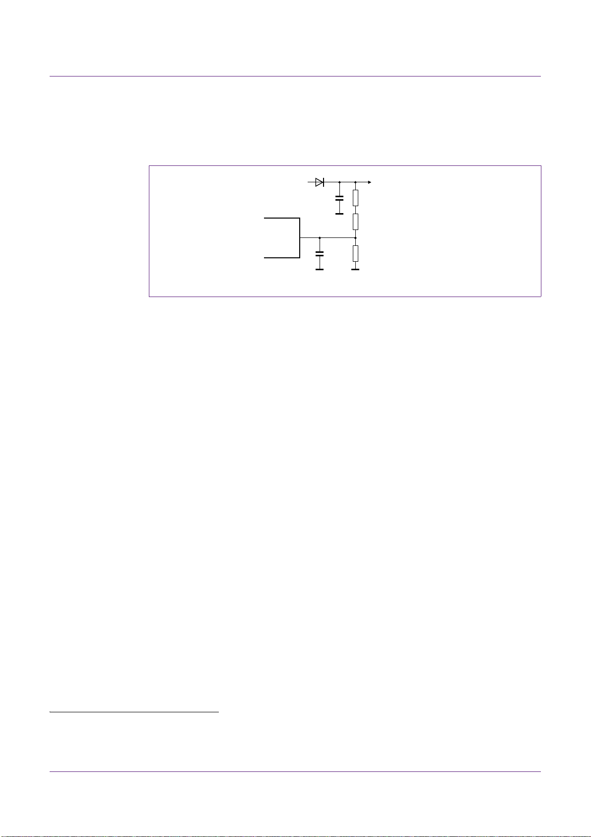
NXP Semiconductors
001aal026
4.7 MΩ
4.7 MΩ
4.7 nF
R
measure(SNSBOOST)
60 kΩ
24
SNSBOOST
PFC stage VBOOST
R
BOOST
TEA1713
R
measure SNSBOOST
R
BOOSTVreg SNSBOOST
V
BOOSTVreg SNSBOOST
–
--------------------------------------------------------------- -
=
R
measure SNSBOOST
R
BOOSTVreg SNSBOOST
V
BOOSTVreg SNSBOOST
–
--------------------------------------------------------------- -
9.4 M 2.5 V
394 V2.5 V–
-------------------------------------- -
60 k===
7.2 PFC regulation
AN10881
TEA1713 resonant power supply control IC with PFC
7.2.1 Sensing V
Fig 16. PFC output regulation example: SNSBOOST
The boost output voltage value is set with a resistor divider between the PFC output
voltage and pin SNSBOOST. When in regulation, the SNSBOOST voltage is kept at 2.5 V.
The resistor divider can have a total value up to 10 M to limit power loss.
The measurement resistor between SNSBOOST and ground can be calcul ated with the
following equation:
BOOST
(6)
1.The TEA1713 PFC, operates in Quasi Resonant (QR) mode with valley detection providing good efficiency. Valley detection
needs additional ringing time within every switching cycle. This time for ringing adds short periods of no power transfer to the
output capacitor. The system must compensate this with a somewhat higher peak current. A rule of thumb is that the peak current
in QR mode is a maximum of 10 % higher than the calculated peak current in Critical conduction mode.
AN10881 All information provided in this document is subject to legal disclaimers. © NXP B.V. 2011. All rights reserved.
Application note Rev. 2 — 26 September 2011 35 of 102
Example:
• R
measure(RBOOST)
• V
BOOST
=394V
=4.7M +4.7M =9.4M
Use a capacitor on SNSBOOST to prevent wrong measurements due to MOSFET
switching noise, mains surge events or ESD events. Also, for this reason, place the
measurement resistor and the filtering capacitor close to the IC in the PCB layout.
7.2.2 SNSBOOST open and short circuit pin detection
The PFC does not start switching until the voltage on SNSBOOST is above 0.4 V. This
serves as short circuit protection for the boost voltage and SNSBOOST pin itself.
An internal current source draws a small amount of current from SNSBOOST. This
prevents switching when the pin is left open as the volt a ge remains lower than 0.4 V. This
combination also creates an Open-Loop Protection (OLP) when, for example, one of the
resistors in the boost divider network is disconnected.
(7)
Page 36

NXP Semiconductors
001aal027
MAINS
VOLT AGE
R
BOOST
4.7 MΩ
R
BOOST
4.7 MΩ
4.7 nF
C
comp1
C4
R4
R3
R2
R1
CX1
C
comp2
R
comp
g
m
R
measure(SNSBOOST)
60 kΩ
24
t
ON
2
K
SNSBOOST
SNSMAINS
1COMPPFC
2.5 V
VBOOST
TEA1713
f
z
1
2 R
compCcomp2
---------------------------------------------------
=
f
p
C
comp1Ccomp2
+
2 R
compCcomp1Ccomp2
-------------------------------------------------------------------------- -
=
7.2.3 PFCCOMP in the PFC voltage control loop
SNSBOOST sets and controls the PFC output voltage. The internal error amplifier with a
reference voltage of 2.5 V senses the voltage at SNSBOOST. The amplifier converts the
input error voltage with a transconductance g
available at COMPPFC for adding an external loop compensation network. The current
from the error amplifier results in a loop voltage at COMPPFC. This COMPPFC voltage, in
combination with the voltage at pin SNSMAINS, determines the PFC switching-on time.
A compensation network, typically comprising one resistor and two capacitors at pin
COMPPFC, is used to stabilize the PFC control loop.
AN10881
TEA1713 resonant power supply control IC with PFC
=80A/V to its output. This output is
m
Fig 17. Basic PFC voltage control loop with PFCCOMP
The transfer function has a pole at 0 Hz, a zero by R
C
comp1/Ccomp2
. Set the zero frequency to 10 Hz while the next pole frequency is at 40 Hz.
comp/Ccomp2
and a pole again by
The zero point and pole frequencies of the compensation network can be calculated as
follows:
The choice also concerns a trade-off between power factor and transient behavior. A
lower regulation bandwidth leads to a better power factor but the transient behavior
AN10881 All information provided in this document is subject to legal disclaimers. © NXP B.V. 2011. All rights reserved.
Application note Rev. 2 — 26 September 2011 36 of 102
becomes poorer. A higher regulation bandwidth leads to a be tter transie nt respon se but a
poorer power factor.
(8)
(9)
Page 37

NXP Semiconductors
KV
mains
A
V
mains
2
--------------- -
=
on-time
V
max-ton
V
zero-ton
V
PFCCOMP
001aal028
0
t
on,max(lowmains)
t
on,max(highmains)
V
SNSMAINS
= 0.9 V
V
SNSMAINS
= 3.3 V
7.2.4 Mains compensation in the PFC voltage control loop
The mathematical equation for the transfer function of a power factor corrector, contains
the square of the mains input voltage.
In a typical application this results in a low bandwidth for low mains input voltages, while at
high mains input voltages the MHR requirements can be hard to meet.
The TEA1713 contains a correction circuit to compensate for the mains input voltage
influence. SNSMAINS measures the average mains voltage, which is used for internal
compensation. Figure 18
COMPPFC voltage and the on-time. With this compensation it is possible to keep the
regulation loop bandwidth constan t over th e co mplete main s inp ut voltage range, yielding
a fast transient response on load steps, while still complying with class-D MHR
requirements.
AN10881
TEA1713 resonant power supply control IC with PFC
(10)
shows the relationship between the SNSMAINS voltage,
Fig 18. Relationship between on-time SNSMAINS voltage and COMPPFC voltage
7.3 PFC demagnetization and valley sensing
The PFC MOSFET is switched on for the next stroke, if the voltage at the drain of the
MOSFET is at its minimum (valley switching), to reduce switching losses and EMI
(see Figure 19
AN10881 All information provided in this document is subject to legal disclaimers. © NXP B.V. 2011. All rights reserved.
Application note Rev. 2 — 26 September 2011 37 of 102
).
Page 38

NXP Semiconductors
demagnetized
V
Rect
/N
V
Rect
V
Boost
(V
Boost
− V
Rect
)/N
V
aux,demag
0
0
magnetized
Demagnetization
l
TrPfc
AuxPfc
DrPfc
GatePfc
Valley
(= top for detection)
0
off
on
t
001aal029
N
aux max
V
SNSAUXPFC
V
Lmax
------------------------------ -
N
p
25 V
415
-----------
52 3.13 3 turns===
AN10881
TEA1713 resonant power supply control IC with PFC
Fig 19. PFC demagnetization and valley sensing
SNSAUXPFC detects the valleys. An auxiliary winding on the PFC coil provides a
measurement signal on SNSAUXPFC. It gives a reduced and inverted copy of the
MOSFET drain voltage. When a valley of the drain voltage (top at SNSAUXPFC voltage)
is detected, the MOSFET is switched on.
If no top (valley at the drain) is detected on SNSAUXPFC within 4 s after
demagnetization is detected, the MOSFET is forced to switch on.
7.3.1 PFC auxiliary sensing circuit
Add a 5 kseries resistor to SNSAUXPFC to protect the internal circuit of the IC against
excessive voltage, for example during lightning surges. In the PCB layout, place this
resistor close to the IC to prevent disturbances causing incorrect switching.
It is important to maintain valley detection even at low ringing amplitudes. Set the voltage
at the SNSAUXPFC as high as possible, while taking into account its absolute maximum
rating of 25 V.
The number of turns of the auxiliary winding on the PFC coil can be calculated using the
following equation:
(11)
AN10881 All information provided in this document is subject to legal disclaimers. © NXP B.V. 2011. All rights reserved.
Application note Rev. 2 — 26 September 2011 38 of 102
Page 39

NXP Semiconductors
V
Lmax
V
OVP SNSBOOST
V
reg SNSBOOST
---------------------------------------- -
V
BOOST
2.63 V
2.5 V
--------------- -
394 V 415 V===
R
SENSE PFC
V
OCR SNSCURPFC
V–
minarg
I
P
max
-----------------------------------------------------------------------
0.52 V 0.1 V–
8.73 A
------------------------------------ -
48 m===
Where:
AN10881
TEA1713 resonant power supply control IC with PFC
• V
SNSAUXPFC
• V
Lmax
• N
is the number of turns on the PFC coil (for this example, a value of 52 is used)
P
is the absolute maximum voltage rating
is the maximum voltage across the PFC primary winding
The boost output voltage at OverVoltage Protection (OVP) determines the maximum
voltage across the PFC primary winding and can be calculated using the following
equation:
In this example, a design value of 394 V is used for nominal
When a PFC coil with a higher number of auxiliary turns is used, a resistor voltage divider
can be placed between the auxiliary winding and SNSAUXPFC. The total resistive value
of the divider must be less than 10 k to prevent delay of the valley detection in
combination with parasitic capacitances.
7.3.2 PFC frequency limit
The switching frequency is limited to 125 kHz to minimize the switching losses. If the
frequency for quasi-resonant operation is above the 125 kHz limit, the system switches
over to Discontinuous conduction mode. The PFC MOSFET is only switched on at a
minimum voltage across the switch (valley switching). One or more valleys are skipped,
when necessary, to keep the frequency below 125 kHz (valley skipping).
V
BOOST
(12)
.
The minimum off-time is limited to 50 s after the last PFC gate signal to ensure proper
control of the PFC MOSFET under all circumstances.
7.4 PFC OverCurrent Regulation/Protection (OCR/OCP)
The maximum peak current, switched by the external MOSFET, is limited cycle-by-cycle
by sensing the voltage across a measurement resistor R
SENSE(PFC)
MOSFET. SNSCURPFC measures the voltage, which is limited to 0.5 V. At this voltage
level the MOSFET is switched off.
Take a small voltage margin into account to avoid false triggering of the OCP.
The value of the measurement resistor R
SENSE(PFC)
can be calculated with Equation 13:
The SNSCURPFC voltage senses an initial voltage peak at the moment the PFC
MOSFET switches on, because its (parasitic) capacitance s are discharged. SN SCURPFC
has a leading edge blanking of 310 ns to mask this event, so it does not react to this initial
peak.
in the source of the
(13)
AN10881 All information provided in this document is subject to legal disclaimers. © NXP B.V. 2011. All rights reserved.
Application note Rev. 2 — 26 September 2011 39 of 102
Page 40

NXP Semiconductors
001aal030
60 μA
typ
R
SENSE(PFC)
R
SS
≥ 12 kΩ
C
SS
COMP
SNSCURPFC
0.5 V
CONTROL
4
TEA1713
RSSCSS=
7.4.1 PFC soft-start and soft-stop
The PFC has a soft-start function and a soft-sto p function to prevent transformer
noise/rattle at start-up or during Burst mode operation. The soft-start slowly increase s the
primary peak current at the start of operation. The soft- stop function slowly de crea ses the
transformer peak current before operation is stopped.
Fig 20. PFC soft-start and soft-stop setup
AN10881
TEA1713 resonant power supply control IC with PFC
A resistor and a capacitor between SNSCURPFC and th e curr en t s ense res is to r
R
SENSE(PFC)
7.4.1.1 Soft-start
Before start of operation, an internal current source of 60 A charges the capacitor to
V
SNSCURPFC
0.5 V, the operation can start. Select a resistor R
voltage level is reached. At start-up, the current source is stopped and the voltage on
SNSCURPFC drops as R
each cycle increases until C
regulation level (OCR/OCP), set by R
The soft-start period can be claclulated with Equation 14
7.4.1.2 Soft-stop
Soft-stop is achieved by switching on the internal current source of 60 A again.
The current charges C
When SNSCURPFC reaches 0.5 V the operation is stopped.
The voltage is only measured during the off-time of the PFC power switch to prevent
measurement disturbances during soft-stop.
set both functions.
=60A RSS. When SNSCURPFC exceeds the internal start voltage of
12 k to ensure that the start
SS
discharges CSS. During this discharge the peak current of
SS
is discharged completely and the normal peak current
SS
SENSE(PFC)
, is reached.
:
and the increasing capacitor voltage reduces the peak current.
SS
(14)
7.4.2 SNSCURPFC open and short protection
When the SNSCURPFC pin is open, SNSCURPFC is charged to 0.5 V by the internal
current source of 60 A for soft-start. The PFC does not start switching because of OCP.
When the SNSCURPFC pin is short circuit to ground, the PFC cannot start operation as
the start level of 0.5 V has not been reached.
AN10881 All information provided in this document is subject to legal disclaimers. © NXP B.V. 2011. All rights reserved.
Application note Rev. 2 — 26 September 2011 40 of 102
Page 41
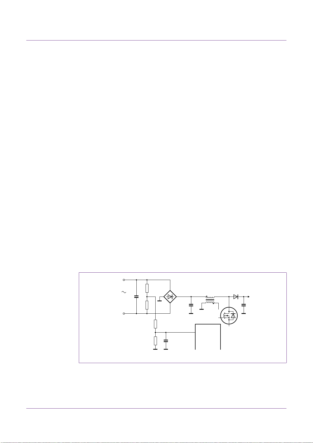
NXP Semiconductors
V
OVP BOOST
V
OVP SNSBOOST
V
reg SNSBOOST
---------------------------------------- -
V
BOOST
2.63 V
2.5 V
--------------- -
394 V 415 V===
001aal031
MAINS
VOLT AGE
C4
R4
R3
R2
R1
CX1
2
SNSMAINS
TEA1713
7.5 PFC boost OverVoltage Protection (OVP)
An overvoltage protection circuit is built in to prevent boost overvoltage during load steps
and mains transients. When the voltage on SNSBOOST exceeds 2.63 V, the switching of
the power factor correction circuit is stopped. The PFC resumes switching when the
voltage on SNSBOOST drops below 2.63 V.
When the resistor between pin SNSBOOST and ground is open, the overvoltage
protection also triggers. In this situation, an internal current source of 45 nA to ground can
increase the voltage on SNSBOOST to the OVP protection level.
The voltage value at which PFC OVP becomes a ctive can be calcul ated with the followin g
equation:
AN10881
TEA1713 resonant power supply control IC with PFC
(15)
In the example, a design value of 394 V is used for nominal
V
BOOST
.
7.6 PFC mains UnderVoltage Pr otection (brownout protection)
The voltage on the SNSMAINS pin is sensed continuously to prevent the PFC operating
at very low mains input voltages. When the voltage on this pin drops below 0.89 V, the
switching of the PFC is stopped. This mains undervoltage protection is sometimes
referred to brownout protection.
The voltage on pin SNSMAINS must be an average DC value that represents the mains
input voltage. The system works best with a time constant of approximately 150 ms for pin
SNSMAINS. When the voltage on SNSMAINS drops, it is internally clamped to a value of
1.05 V, which is 0.1 V below the start level of 1.15 V for SNSMAINS. This allows a fast
restart when the mains input voltage returns after a mains-dropout. The PFC (re)sta rts
when the SNSMAINS voltage exceeds the star t level of 1.15 V.
AN10881 All information provided in this document is subject to legal disclaimers. © NXP B.V. 2011. All rights reserved.
Application note Rev. 2 — 26 September 2011 41 of 102
Fig 21. SNSMAINS circuitry
Page 42

NXP Semiconductors
V
AC
average
22
----------
V
AC
rms
=
R
v
R1 R2
R1 R2+
------------------- -
=
V
BO
2
22
----------
V
SNSMAINS UVP
RvR3+
R4
------------------ -
1+
=
V
BO
2
22
----------
0.89
R
v
R3+
R4
------------------ -
1+
=
66 1.9771
1 M R3+
R4
--------------------------- -
1+
=
t
SNSMAINS
R4 C4 47 k 3300 nF 155 ms== =
R
disch earg
R1
R2 R3 R4+
R2 R3 R4++
------------------------------------- -
+=
7.6.1 Undervoltage or brownout protection level
The AC input voltage is measured via R1 and R2. Each resistor alternately senses half
the sine cycle and as a result, both resistors have the same value.
A typical resistor value of 2 M can be applied for R1and R2 to keep the bleeder loss low.
The average voltage sensed is calculated as follows:
AN10881
TEA1713 resonant power supply control IC with PFC
(16)
The SNSMAINS brownout protection (RMS) voltage level is calculated with Equation 17
(17)
(18)
Example:
Required: V
• V
SNSMAINS(UVP)
• R1=R2=2MR
= 66 V (AC), with:
BO
=0.89V
=1M
V
(19)
(20)
R3 = 560 k, R4 = 47 k
The time constant for a recommended time constant of 150 ms, with C4 = 3300 nF:
:
7.6.2 Discharging the mains input capacitor
There is often an application requirement to discharge the X capacitors in the EMC input
filtering within a certain time. The replacement values of R1, R2, R3 and R4 determine the
resistance required for discharging the X ca pa citors in the input filte ring. The replacement
value can be calculated with Equation 21
AN10881 All information provided in this document is subject to legal disclaimers. © NXP B.V. 2011. All rights reserved.
Application note Rev. 2 — 26 September 2011 42 of 102
:
(21)
Page 43

NXP Semiconductors
R
disch earg
R1
R2 R3 R4+
R2 R3 R4++
------------------------------------- -
2 M
2 M 560 k 47 k+
2 M 560 k 47 k++
------------------------------------------------------------------ -
2465 k=+=+=
Example:
AN10881
TEA1713 resonant power supply control IC with PFC
Required: t
discharge
< 600 ms, with:
• R1=R2=2M
• R3 = 560 k
• R4 = 47 k
Where:
• C=220nF
• The time constant equals: t
7.6.3 SNSMAINS open pin detection
The SNSMAINS pin, which senses the mains input voltage, has an integrated protection
circuit to detect an open pin. When the pin is not connected, an internal current source of
33 nA either pulls the pin down below the stop level of 0.9 V or keeps it below the start
level of 1.15 V.
When the SNSMAINS pin is shorted to ground, the results are similar.
discharge=Rdischarge
(22)
C = 2465 k220nF=542ms
AN10881 All information provided in this document is subject to legal disclaimers. © NXP B.V. 2011. All rights reserved.
Application note Rev. 2 — 26 September 2011 43 of 102
Page 44

NXP Semiconductors
8. HBC functions
8.1 HBC UVP boost
The TEA1713 begins operation when the inp ut volt age is high er than approximatel y 90 %
of the nominal boost voltage to ensure proper working of the HBC.
The voltage on the SNSBOOST pin is sensed continuously. When the voltage on
SNSBOOST drops below 1.6 V, switching of the HBC is stopped when the low-side
MOSFET is on. The HBC (re)starts when the SNSBOOST voltage exceeds the start level
of 2.3 V.
8.2 HBC switch control
The internal control for the MOSFET drivers, determines when the MOSFETs are
switched on and off. It uses the input from several functions.
1. An internal divider is used to provide the alternating switching of high-side and
2. The adaptive non-overlap (see Section 8.3
3. The oscillator (see Section 8.4
4. Several protection and enable functions determine if the resonant converter is allowed
AN10881
TEA1713 resonant power supply control IC with PFC
low-side MOSFET for every oscillator cycle.
) sensing on HB determines the switch-on
moment.
) determines the switch-off moment.
to switch.
8.3 HBC adaptive non-overlap
8.3.1 Inductive mode (normal operation)
The high efficiency of a resonant converter is the result of Zero-Voltage Switching (ZVS)
of the power MOSFETs, also called soft-switching. A small non-overlap time (also called
dead time) is required between the on-time of the high-side MOSFET and low-side
MOSFET to allow soft-switching. During this non-overlap time, the primary resonant
current (dis)charges the capacit ance of the half-bridge between ground and boost volt age.
After the (dis)charge, the body diode of the MOSFET starts conducting and because the
voltage across the MOSFET is zero, there are no switching losses.
This mode of operation is called Inductive mode beca us e th e switc hin g freq ue n cy is
above the resonance frequency and the resonant tank has an inductive impedance.
AN10881 All information provided in this document is subject to legal disclaimers. © NXP B.V. 2011. All rights reserved.
Application note Rev. 2 — 26 September 2011 44 of 102
Page 45
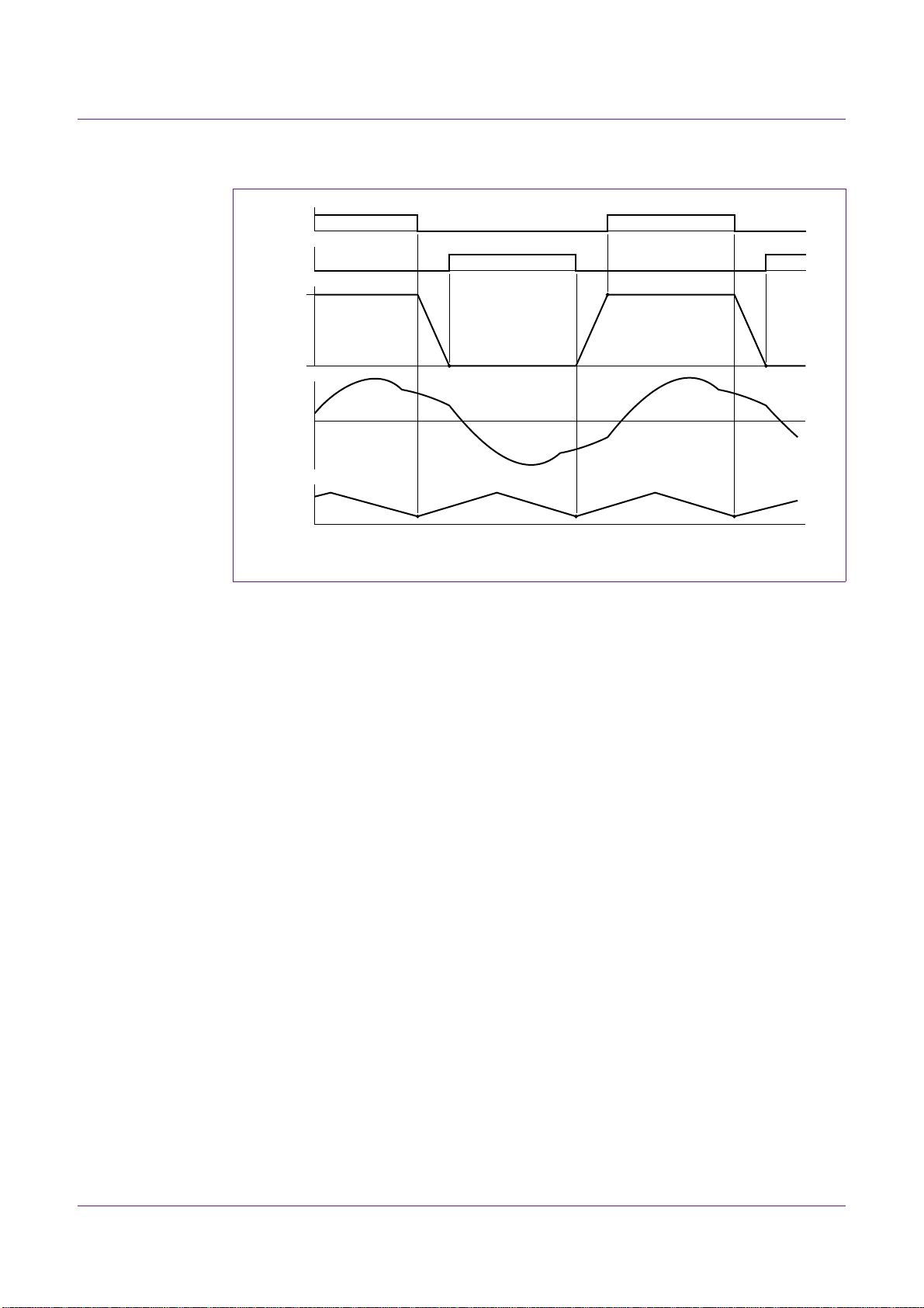
NXP Semiconductors
GateLs
GateHs
Hb
I
TrHbc
Cfmin
t
V
Boost
0
001aal032
AN10881
TEA1713 resonant power supply control IC with PFC
Fig 22. Inductive mode HBC switching
The time required for the transition of the HB depends on the amplitude of the resonant
current at the moment of switching. There is a (complex) relationship between the
amplitude, the frequency, the boost voltage and the output voltage. Ideally the IC switches
on the MOSFET when the transition of the HB has reached its end value. It must not wait
longer, espe cially at high output load, to prevent a swing back of the HB voltage.
The adaptive non-overlap function of the TEA1713 provides an automatic measurement
and control function that decides when to switch on. As it uses actual measurement input
the control adapts for operation changes in time.
Because of this adaptive non-overlap function, it is not necessary to preset a fixed
non-overlap time, which is always a compromise between different operating conditions.
The adaptive non-overlap function senses the slope at HB after one MOSFET has been
switched off. Normally, the slope at the HB starts directly. Once the transition of the HB
node is complete, the slope ends. This is detected by the adaptive non-overlap sensing
and the other MOSFET is switched on. In this way the non-overlap time is automatically
adjusted to the best value providing the lowest switching loss, even if the HB transition
cannot be fully completed.
AN10881 All information provided in this document is subject to legal disclaimers. © NXP B.V. 2011. All rights reserved.
Application note Rev. 2 — 26 September 2011 45 of 102
Page 46

NXP Semiconductors
fast HB slope
V
Boost
Hb
GateLs
GateHs
0
slow HB slope incomplete HB slope
t
001aal033
Fig 23. Adaptive non-overlap switching during normal operating conditions
The non-overlap time depends on the HB slope, but has an upper and lower time limit. An
integrated minimum non-overlap time (160 ns
all conditions. The maximum non-overlap tim e is limited to the charging time of the
oscillator. If the HB slope takes more time than the charging of the oscillator (25 % of HB
switching period) the MOSFET is forced to switch on. In this case the MOSFET is not
soft-switching. This limitation of the maximum non-overlap time ensures that at high
switching frequency the on-time of the MOSFET is at least 25 % of the HB switching
period.
AN10881
TEA1713 resonant power supply control IC with PFC
) prevents accidental cross conduction in
max
8.3.2 Capacitive mode
During error conditions (e.g. output short circ uit , load pu lse to o hig h) or specia l sta rt- up
conditions, the switching frequency can become lower than the resonance frequency. The
resonant tank then has a capacitive impedance. In Capacitive mode the HB slope does
not start after the MOSFET has switched off. It is not preferred to just switch on the other
MOSFET. The lack of soft-switching increases dissipation in the MOSFETs. The
conducting body diode in the MOSFET at the switching moment can damage or even
destroy the device quickly.
AN10881 All information provided in this document is subject to legal disclaimers. © NXP B.V. 2011. All rights reserved.
Application note Rev. 2 — 26 September 2011 46 of 102
Page 47

NXP Semiconductors
0
t
001aal034
delayed
oscillator
delayed switch-on
during capacitive mode
no HB slope
wrong polarity
GateHs
GateLs
0
V
Boost
Hb
0
0
0
I
TrHbc
Cfmin
AN10881
TEA1713 resonant power supply control IC with PFC
Fig 24. Capacitive mode HBC switching
The adaptive non-overlap system of the TEA1713 always waits until the slope at the
half-bridge node starts. It guarantees safe/best switching of the MOSFETs in all
circumstances. In Capacitive mode, it can take half the resonanc e pe rio d befor e the
resonant current changes back to the correct polarity and starts charging the half-bridge
node. The oscillator remains in its slow charging current mode until the half-bridge slope
starts to allow this relatively long waiting time (see also Section 8.4.2
and Figure 28).
The MOSFET is forced to switch on when the half-bridge slope does not start at all and
the slowed-down oscillator reaches the high level.
The Capacitive Mode Regulation (CMR) function increases the oscillation frequency to
bring the converter from Capacitive mode to Inductive mode operation again.
8.3.3 Capacitive Mode Regulation (CMR)
The adaptive non-overlap function prevents the harmful switching in Capacitive mode.
However, an extra action is executed, which results in the CMR to end the Capacitive
mode operation and return to Inductive mode operation.
Capacitive mode is detected when the HB slope does not start shortly (690 ns) after the
MOSFET is switched-off. At detection of Capacitive mode, the switching frequency is
increased quickly. This is realized by discharging SSHBC/EN with a high current
(1800 A) from the moment t
no-slope
= 690 ns has passed before the half -b rid ge s lop e
starts. The resulting frequency increase regulates the HBC back to the border between
Capacitive mode and Inductive mode.
AN10881 All information provided in this document is subject to legal disclaimers. © NXP B.V. 2011. All rights reserved.
Application note Rev. 2 — 26 September 2011 47 of 102
Page 48

NXP Semiconductors
001aal035
load independent point
(series resonance)
f0
@ Vimax
@ Qmax
@ Qnom @ Qmin
@ Vinom
@ Vimin
Mmin
Mnom
1
Mmax
resistive
inductivecapactive
fl fr fmax f
M =
V
i
a·V
o
001aal036
Typical behavior at capacitive
mode protection/regulation
Frequency increaseby capacitive
mode protection/regulation
(notice voltage drop on SSHBC/EN)
HBHB
SNSCURHBC
SSHBC/EN
Voutput
CFMIN
SSHBC/EN
Voutput
AN10881
TEA1713 resonant power supply control IC with PFC
Fig 25. Capacitive/Inductive HBC operating frequencies
CMR of the TEA1713 can be recognized by the typical slowing of the oscillator in
combination with the discharging of SSHBC/EN.
Oscilloscope traces contain normal time-base (top) and zoomed view (bottom)
Fig 26. Typical protection and regulation behavior in Capacitive mode (during bad start-up)
AN10881 All information provided in this document is subject to legal disclaimers. © NXP B.V. 2011. All rights reserved.
Application note Rev. 2 — 26 September 2011 48 of 102
Page 49

NXP Semiconductors
f
HB,limit
f
max,B
V
fmax
V
RFMAX
A
curve C
fminRfmax
A high high
B low low
C low too low
B
C
f
max,A
f
min,
B and C
f
min,A
0
f
HB
001aal037
8.4 HBC oscillator
The slope controlled oscillator determines the switching frequency of the half-bridge. The
oscillator generates a triangular waveform at the external capacitor Cf
8.4.1 Presettings
Two external components determine the frequency range:
• Capacitor at CFMIN
• Resistor at RFMAX
The oscillator frequency depends on the charge and discharge current of the capacitor on
CFMIN. This (dis)charge current consists of a fixed part which determines the minimum
frequency, and a variable part which depends on the value of the resistor on RFMAX and
the voltage at pin RFMAX.
• The voltage on RFMAX is 0 V when the oscillator frequency is minimum.
• The voltage on RFMAX is 2.5 V when the oscillator frequency is maximum.
• The value of the resistor on RFMAX determines the relationship between VRFMAX
AN10881
TEA1713 resonant power supply control IC with PFC
.
min
Sets the minimum frequency in combination with an internally trimmed current source.
Sets the frequency range and, in combination with CFMIN, the maximum freq uency.
and the frequency. It also determines the maximum frequency when RFMAX = 2.5 V .
The maximum frequency of the oscillator is independent of the settings on CFMIN and
RFMAX and is limited internally to a minimum of 500 kHz. Figure 27
relationship between VRFMAX and f
Fig 27. Frequency relationships
8.4.2 Operational control
During operation, the state of the half-bridge node HB controls the oscillator is. An internal
slope detection circuit monitors the voltage on HB to achieve this.
for three different values of C
HB
shows the
and R
fmin
fmax
.
The charge current of the oscillator is initially set to a low value of 30 A. After the start of
the half-bridge slope has been detected, the charge current is increased to the normal
value that corresponds to the working frequency at that moment. Feedback on SNSFB
controls the working frequency. Normally, the half-bridge slope starts directly after the
switch-off of the MOSFET, the time with the low oscillator current (30 A) being negligible.
AN10881 All information provided in this document is subject to legal disclaimers. © NXP B.V. 2011. All rights reserved.
Application note Rev. 2 — 26 September 2011 49 of 102
Page 50

NXP Semiconductors
GateLs
GateHs
Hb
30 μA-period
I
TrHbc
Cfmin
t
V
Boost
0
0
001aal038
f
oscillator
2f
HB
=
t
ch eargtdisch earg
t
oscillator
2
--------------------- -
V
oscillator
V
high CFMINVlow CFMIN
3 V1 V2 V=–=–=
I
oscillator min
150 A=
The similarity between GA TELS and GATEHS when switching, is that the oscillator signal
determines the moment of switching off. The HB sensing circuit determines the moment of
switching on.
As the HB sensing (and therefore not fixed) determines the moment of switching on, the
time between switching one MOSFET off and the other one on, is adaptive: adaptive
non-overlap time (or dead time). This non-overlap time has no influence on the oscillator
signal.
The frequency control by oscillator-frequency consists of determining the time between
two moments of switching off (including a small period in which the oscillator current is
only 30 A).
AN10881
TEA1713 resonant power supply control IC with PFC
AN10881 All information provided in this document is subject to legal disclaimers. © NXP B.V. 2011. All rights reserved.
Application note Rev. 2 — 26 September 2011 50 of 102
Fig 28. Timing overview of the oscillator and HBC drive
8.4.3 CFMIN and RFMAX
This section explains the method of calculating the values for the cap acitor on CFMIN and
the resistor on RFMAX.
8.4.3.1 Minimum frequency setting for CFMIN
(23)
(24)
(25)
(26)
Page 51

NXP Semiconductors
CFMIN
I
oscillator min
22 f
HB min
V
oscillator
----------------------------------------------------------------------- -
150 A
8f
HB min
----------------------------
==
CFMIN
150 A
22 57 kHz 2
--------------------------------------------- -
0.00015
456000
------------------ -
329 pF===
I
oscillator max
4.7 I
RFMAX max
I
oscillator min
+=
I
RFMAX max
V
fmax
RFMAX
-------------------- -
=
RFMAX
V
fmax
I
RFMAX max
----------------------------- -
2.5 V
I
RFMAX max
----------------------------- -
==
f
HB max
I
oscillator max
4CFMIN V
oscillator
---------------------------------------------------------------
4.7 I
RFMAX maxIoscillator min
+
4CFMIN 2
------------------------------------------------------------------------------------
==
I
RFMAX max
8 CFMIN f
HB maxIoscillator min
–
4.7
----------------------------------------------------------------------------------------------- -
=
I
RFMAX max
8CFMIN f
HB max
150 A–
4.7
--------------------------------------------------------------------------------
=
RFMAX
2.5 V
I
RFMAX max
----------------------------- -
11.75
8CFMIN f
HB max
150 A–
--------------------------------------------------------------------------------
==
I
RFMAX max
8 330 pF 180 kHz 150 A–
4.7
-------------------------------------------------------------------------------
475 A150 A–
4.7
----------------------------------------------- -
69.15 A===
RFMAX
2.5 V
69.15 A
---------------------- -
36 k==
Example:
AN10881
TEA1713 resonant power supply control IC with PFC
(27)
Requirement: f
HB(min)
=57kHz
8.4.3.2 Maximum frequency setting for RFMAX
Analog to the situation with I
oscillator(min)
:
(28)
(29)
(30)
(31)
(32)
(33)
(34)
(35)
Example:
Requirement: f
HB(max)
= 180 kHz and CFMIN = 330 pF
(36)
(37)
Remark: The average multiplication factor is 4.7. There is a small deviation in value
depending on other parameters and presetting conditions. Practical verification of the
result is advised.
8.4.4 RFMAX and High Frequency Protection (HFP)
Normally, the converter does not operate continuously at the preset maximum frequency.
This maximum frequency is only used for a short time during soft-start or temporary
fault/overload conditions.
AN10881 All information provided in this document is subject to legal disclaimers. © NXP B.V. 2011. All rights reserved.
Application note Rev. 2 — 26 September 2011 51 of 102
Page 52

NXP Semiconductors
001aal039
V+
8.4 V
3.2 V
21 SNSFB
CONTROL
TEA1713
1.5 kΩ
When the operating frequency remains at, or close to, maximum frequency for a longer
period, a fault condition is assumed and a protection activated.
The HFP senses the voltage at pin RFMAX. This voltage indicates the actual operating
frequency. When the frequency is higher than approximate ly 75 % of the frequency range
(RFMAX = 1.83 V), the protection timer is started.
Remark: During normal regulation, the maximum frequency leads to only 60 of the
present range and the voltage at pin RFMAX is 1.5 V maximum.
8.5 HBC feedback (SNSFB)
A typical power supply application contains mains insulation in the HBC. On the
secondary (mains insulated) side, the output voltage is compared to a reference and
amplified. The TEA1713 is normally placed on the primary side. The output of the error
amplifier is transferred to the primary side via an OPTO coupler. The output of the OPTO
coupler on the primary side can be connected directly to SNSFB.
AN10881
TEA1713 resonant power supply control IC with PFC
Fig 29. T ypical basic SNSFB application
The SNSFB pin supplies the OPTO coupler from an internal voltag e source of 8.4 V via an
internal series resistor of 1.5 k. This internal series resistance allows spike filtering by an
external capacitor at the pin if needed.
The feedback input has a threshold current of 0.66 mA at which the frequency is minimum
to ensure sufficient bias current for proper working of the opto coup ler. The maximum
frequency controlled by SNSFB is reached at 2.2 mA. This is approximately 60 % of the
total preset frequency range. The remaining upper p art of the frequency range can only be
reached by control of SSHBC/EN for soft-start or protection.
AN10881 All information provided in this document is subject to legal disclaimers. © NXP B.V. 2011. All rights reserved.
Application note Rev. 2 — 26 September 2011 52 of 102
Page 53

NXP Semiconductors
0
I
SNSFB
V
open
= 8.4 V
0.66 mA
I
fmin
V
RFMAX
2.2 mA
I
fmax
00
V
SSHBC
= 8 V
260 μA
I
OLP
V
OLP
= 7.7 V
V
fmin
= 6.4 V
V
fmax
= 4.1 V
V
clamp,fmax
= 3.2 V
V
SNSFB
8 mA
I
clamp,max
001aal040
2.5 V
typ
= V
fmax
1.5 V
typ
= 0.6
×
V
fmax
Pout (W)
0 250200100 15050
001aal041
5.4
5.6
5.2
5.8
6.0
SNSFB
(V)
5.0
(1)
(2)
(3)
Fig 30. SNSFB V-I characteristics
AN10881
TEA1713 resonant power supply control IC with PFC
AN10881 All information provided in this document is subject to legal disclaimers. © NXP B.V. 2011. All rights reserved.
Application note Rev. 2 — 26 September 2011 53 of 102
1. V
2. V
3. V
BOOST
BOOST
BOOST
= 310 V (DC)
= 350 V (DC)
= 390 V (DC)
Fig 31. SNSFB voltage to output power characteristics examples
8.5.1 HBC Open-Loop Protection (OLP)
The resonant controller of the TEA1713 contai ns an Open-Loop Protection (OLP). This
protection monitors the voltage on SNSFB. When it exceeds 7.7 V, the protection timer is
started.
In normal operating conditions, the OPTO coupler current is between 0.66 mA and 2.2 mA
which pulls down the voltage at pin SNSFB. Due to an error in the feedback loop, the
current can become less than 260 A which leads to an open-loop protection.
Page 54

NXP Semiconductors
001aal042
SSHBC/EN 22
1360 μA
440 μA
120 μA
40 μA
120 μA
40 μA
5 μA
high CMR
disable
1.2 V
ENABLE PFC
COMP
low CMR high SoSt low SoSt bias
TEA1713
2.2 V
ENABLE HBC
COMP
FREQUENCY
CONTROL
8 V
3.2 V
42 μA
3.0 V
8.4 V
8.6 SSHBC/EN soft-start and enable
The SSHBC/EN pin provides the following three functions:
• It enables the PFC (> 1.2 V) and PFC plus HBC (> 2.2 V)
• It performs an HBC frequency sweep during soft-start from 3.2 V to 8 V
• It provides frequency control during protection
Seven internal current sources operate the frequency control depending on the required
action.
• Soft-start + OverCurrent Protection: high/low charge (160 A/40 A) + high/low
• Capacitive mode regulation: high/low discharge (1800A/440 A)
• General: bias discharge (5 mA)
AN10881
TEA1713 resonant power supply control IC with PFC
discharge (160 A/40 A)
Fig 32. SSHBC: overview of sources, clamps and levels
8.6.1 Switching ON and OFF using an external control function
The SSHBC/EN can be used to switch the converters on and off using an external control
function.
This function is often driven by a microcontroller from the secondary side of the OPTO
coupler. The main power supply (PFC+HBC) can be switched off for Standby mode and
AN10881 All information provided in this document is subject to legal disclaimers. © NXP B.V. 2011. All rights reserved.
Application note Rev. 2 — 26 September 2011 54 of 102
switched on for normal operation. A separate standby supply must supply the
microcontroller functions during Standby mode. It is also possible to switch/keep off the
HBC and only have the PFC operational.
Page 55

NXP Semiconductors
The TEA1713 also offers the possibility to switch on/off using the SNSOUT function. This
function is intended for Burst mode operation where the duration of the on-states an d
off-states are short.
AN10881
TEA1713 resonant power supply control IC with PFC
8.6.1.1
Switching ON and OFF using SSHBC/EN
When a voltage is present at pin SUPHV or at pin SUPIC, a current from the SSHBC/EN
pin charges the external capacitor. If the pin is not pulled-down, this current increases the
voltage to 8.4 V. Since this is above the level to enable the operation of PFC (1.2V) and
PFC + HBC (2.2 V), the IC is completely enabled.
The IC can be completely disabled by pulling down the SSHBC/EN pin below 1.2 V. The
PFC controller stops switching immediately, but the HBC continues until the low-side
stroke is active. The pull-down current must be larger than the current capability from the
internal soft-start clamp, i.e. 42 A.
PFC only active
By pulling the SSHBC/EN voltage below the enable PFC + HBC operation level (2.2 V),
but keeping it above the enable PFC operating level (1.2 V), only the HBC is disabled.
This can be used when there is another power converter connected to the boost voltage
of the PFC. The low-side power switch of the HBC is on when the HBC is disabled via the
SSHBC/EN pin.
HBC only active
The TEA1713 is not designed to provide this operation mode but it can be realized by
forcing a voltage higher than 2.63 V (but below 5 V) on SNSBOOST. This way the output
overvoltage protection of the PFC is activated and the PFC operation stopped (put on
hold). The HBC operates because SNSBOOST exceeds its start level of 2.3 V
(boost UVP).
This mode of operation is not likely to be required by an application, but it can be u seful for
starting up and debugging purposes during analyses or eva luation.
8.6.1.2 Hold and continue
The SNSOUT function can be used to start and stop the PFC and HBC. This method is
intended for Burst mode operation to switch off the converters for only a short time. It is
possible to operate only the HBC in Burst mode or both HBC + PFC simultaneously. The
possibilities are similar to SSHBC/EN with the main difference being that HBC continues
without soft-start (see Section 9.1
).
8.6.2 Soft-start HBC
SSHBC/EN provides the soft-start function for the resonant converter.
The relation between switching frequency and output current/power is not constant. It is
highly dependent on output and boost voltage and the relationship can be complex. The
TEA1713 has a soft-start function to ensure that the resonant converter starts or restarts
with safe currents.
The soft-start function forces a start at high frequency so that currents are acceptable in
all conditions. The soft-start slowly decreases the frequency until the outp ut voltage
regulation has taken over the frequency control. The limit ation of the output cur rent during
start-up also limits the output voltage rise and prevents an overshoot.
AN10881 All information provided in this document is subject to legal disclaimers. © NXP B.V. 2011. All rights reserved.
Application note Rev. 2 — 26 September 2011 55 of 102
Page 56

NXP Semiconductors
f
HB
0
V
SSHBC
V
fmax(ss)
= 2.5 V
V
RFMAX
f
min
f
max
0
3.2 V = V
fmax(SSHBC)
8 V = V
fmin(SSHBC)
8.4 V = V
clamp(SSHBC)
3.0 V = V
pu(EN)
I
SNSFB
< 0.66 mA (not yet regulating)
0.66 mA < I
SNSFB
< 2.2 mA (regulating)
V
RFMAX
f
HB
001aal043
During soft-start, in parallel to the soft-start frequency sweep, the SNSCURHBC function
monitors the primary current and can activate regulation in a (temporary) overpower
situation.
The soft-start uses the voltage on pin SSHBC/EN. an external capacitor on SSHBC/EN
sets the timing (duration) of the soft-start event.
As the SSHBC/EN is also used as enable input, the soft-start functionality is above the
enable related voltage levels (see Figure 33
8.6.2.1 Soft-start voltage levels
AN10881
TEA1713 resonant power supply control IC with PFC
).
Fig 33. Operating frequencies related to SSHBC/EN voltage
At start-up, the SSHBC/EN voltage is low which corresponds to the maximum frequency.
During the soft-start proce dur e, the exte rn al capacitor is charged, the SSHBC/EN voltage
rises and the frequency decreases. The contribution of the soft-start function ends when
SSHBC/EN is above 8 V.
The SSHBC/EN voltage is clamped at 8.4 V and remains at that level during normal
operation.
When the voltage on SSHBC/EN is reduced during protection or regulation, the volt ag e is
clamped at 3.0 V . This is to provide a quick response so that th e ope ra tin g fr equen cy ca n
be reduced again. Below 3.2 V the discharge current is reduced to 5 A.
8.6.2.2 SSHBC/EN charge and discharge
Initially , at start-up the soft-st art external capacitor o n SSHBC/EN is only charged to obt ain
a decreasing frequency sweep from maximum to operating frequency.
Besides the function to soft-start, SSHBC/EN is also used for regu lation purposes such as
overcurrent regulation. Therefore the voltage on th e ca pacitor on SSHBC/EN can vary by
charging and discharging it by internal current sources.
For example, in case of overcurrent regulation, a continuous alternation betwee n charging
and discharging of the SSHBC/EN capacitor occurs. The SSHBC/EN voltage can be
regulated in this way overruling the signal on the feedback input SNSFB.
AN10881 All information provided in this document is subject to legal disclaimers. © NXP B.V. 2011. All rights reserved.
Application note Rev. 2 — 26 September 2011 56 of 102
Page 57

NXP Semiconductors
500 mV
−500 mV
V
SNSCURHBC
160 μA
40 μA
−40 μA
−160 μA
I
SSHBC/EN
V
SSHBC/EN
8 V
5.6 V
3.2 V
V
Output
V
regulate
0
0
0 t
t
t
t
Fast soft-start sweep (charge and discharge) Slow soft-start sweep (charge and discharge)
001aal044
The (dis)charge current can have a high value 160 A or a low value 40 A. The
two-speed soft-start sweep of the TEA1713 a llows a combination of a short start-up time
of the resonant converter and stable regulation loops such as overcurrent regulation.
In some cases there can be a situation where overcurrent regulation is activated during
the soft-start sequence. This results in a feedback controlled or corrected soft-start.
The fast (dis)charge speed is used for the upper frequency range where VSSHBC/EN is
below 5.6 V. In the upper frequency range the current and power in the converter do not
react strongly to frequency variations.
AN10881
TEA1713 resonant power supply control IC with PFC
Fig 34. OverCurrent Regulation (OCR) during start-up
The slow (dis)charge speed is used for the lower frequency range where VSSHBC/EN is
above 5.6 V. In the lower frequency range the current in the converter reacts strongly to
frequency variations.
Burst mode
AN10881 All information provided in this document is subject to legal disclaimers. © NXP B.V. 2011. All rights reserved.
Application note Rev. 2 — 26 September 2011 57 of 102
The soft-start capacitor is not charged or discharged during the non-operation time in
Burst mode operation. The soft-start voltage does not ch ange during this time.
Page 58

NXP Semiconductors
Protection
0
3.2 V
V
SSHBC/EN
8 V
0
f
min
f
HB
f
max
t
off
on
f
max
forced
fast
sweep
slow sweep regulationregulation
5.6 V
001aal045
8.6.2.3 SNSFB, SSHBC/EN and soft-start reset - operating frequency control
the SNSFB and SSHBC/EN can simultaneously control the operating frequency.
SSHBC/EN is dominant to provide protection and soft-start capability . Additionally, there is
an internal soft-start reset mechanism that overrules both SNSFB and SSHBC/EN control
inputs and immediately sets the frequency to maximum.
8.6.2.4 Soft-start reset
Some protections require a fast correction of the operating frequency to the maximum
value, but they do not have to stop switching. The overcurrent protection is an example
(see Table 4
When this protection is activated, the control input of the oscillator is disconnected
internally from the soft-start capacitor at pin SSHBC/EN and the switching frequency is
immediately set to maximum. In most cases, the change to the maximum switching
frequency restores safe switching operation. Once the voltage at pin SSHBC/EN has
reached 3.2 V, the control input of the oscillator reconnects to the pin and the normal
soft-start sweep follows. Figure 35
downward sweep.
AN10881
TEA1713 resonant power supply control IC with PFC
).
shows the soft-start reset and the two-speed frequency
Fig 35. Soft-start reset and two-speed soft-start
The soft-start reset is al so used to ensure a safe st art-up at maximum frequen cy when the
HBC is enabled by SSHBC/EN or after a restart. The soft-start reset is not used when the
operation has been stopped for Burst mode.
AN10881 All information provided in this document is subject to legal disclaimers. © NXP B.V. 2011. All rights reserved.
Application note Rev. 2 — 26 September 2011 58 of 102
Page 59

NXP Semiconductors
001aal046
BOOST
COMPENSATION
CONTROL
V
SNSBOOST
HBC operational
I
boost-compensation
± I
boost-compensation
V
BOOST
over current protection
1 V
SNSCURHBC17
1.8 V
V
SNSBOOST
0 μA
170 μA
2.5 V 2.63 V
COMP
Rcc
1 kΩ
TEA1713
over current protection
−1 V
COMP
over current regulation
0.5 V
COMP
over current regulation
−0.5 V
COMP
8.7 HBC overcurrent protection and regulation
Measurement of the primary resonant current indicates the level of output power that is
generated by the converter. During a fault or output overload condition, this current often
increases considerable. By monitoring this current and then ta king appropr iate action, the
converter can remain operational during a temporary fault or overload condition.
The resonant controller of the TEA1713 has two functions when in an overcurrent
condition:
• OverCurrent Regulation (OCR) slowly increases the frequency and the protection
• OverCurrent Protection (OCP) steps to maximum frequency
A boost voltage compensation function is included to reduce the variation in the preset
protection level of the resonant current.
AN10881
TEA1713 resonant power supply control IC with PFC
timer is started
AN10881 All information provided in this document is subject to legal disclaimers. © NXP B.V. 2011. All rights reserved.
Application note Rev. 2 — 26 September 2011 59 of 102
Fig 36. SNSCURHBC
8.7.1 HBC overcurrent regulation
The lowest comparator levels of 0.5 V at the SNSCURHBC pin belong to the
OverCurrent Regulation (OCR) level. There is a comparator for both the positive and
negative polarity. If either level is exceeded, the frequency is slowly increased. This is
accomplished by discharging the soft-start capacitor. Every time the OCR level is
exceeded, this state is latched until the next stroke and the soft-start discharge current is
Page 60

NXP Semiconductors
enabled. When both the positive and negative OCR levels are exceeded, the soft-start
discharge current flows continuously. In this way the operating frequency is slowly
increased until the resonant current value just reaches the value permitted by the preset.
The behavior during OCR can be observed on the SSHBC/EN pin as a resultant
regulation voltage.
When an OCR situation is present for a long time, a serious fault condition is assumed.
During OCR the protection timer is activated. The charging of the protection timer is active
approximately a half period cycle after the 0.5 V level is exceeded. If the detection levels
are continuously exceeded, the timer is charged continuously but, if the detection levels
are only sometimes exceeded, the timer is charged accordingly (for details on
charging/discharging of the protection timer refer to Section 10.3.3.4
activated when RCPROT reaches the protection level of 4 V.
8.7.1.1 Start-up
The overcurrent regulation is effective for limiting the output current during start-up. A
smaller soft-start capacitor ca n be chosen which allows faster star t-up. The small soft-st art
capacitor can result in an excessive output current but the OCR function can slow down
the frequency sweep to keep the output current within the limits.
AN10881
TEA1713 resonant power supply control IC with PFC
). The restart state is
8.7.2 HBC overcurrent protection
In most cases the OverCurrent Regulation is able to keep the current below the set
maximum values. However , the OCR can not be fast enou gh to limit the current for cert ain
error conditions. OverCurrent Protection (OCP) is implemented to protect against those
error conditions.
The internal OCP level is set at 1 V for SNSCURHBC. This is significantly higher than
the OCR level of 0.5 V . When the OCP level is reached the frequency immediately jump s
to the maximum via a soft-start reset procedure, followed by a normal sweep down.
The maximum frequency value for soft-start must be selected to sufficiently limit the
output power under these conditions.
The behavior during OCP can be observed on the SSHBC/EN pin as a new soft-start.
Depending on the (over)load or fault condition during this new soft-start, OCR or OCP can
be reactivated.
8.7.3 SNSCURHBC boost voltage compensation
The primary current, also called resonant current, is sensed via pin SNSCURHBC. It
senses the momentary voltage across an external current sense resistor. The use of the
momentary current signal allows a fast overcurrent protection and simplifies the stability of
the overcurrent regulation. The OCR and OCP comparators compare the SNSCURHBC
voltage to the maximum positive and negative values.
The primary current is higher for the same output power when the boost voltage is low. A
boost compensation is included to reduce the d ependency o f the protected ou tput current
level for the boost voltage. The boost compensatio n so urce s a nd sinks a current fr om the
SNSCURHBC pin. This current creates a voltage drop across the series resistor Rcc. A
typical value for this resistor is 1 k.
AN10881 All information provided in this document is subject to legal disclaimers. © NXP B.V. 2011. All rights reserved.
Application note Rev. 2 — 26 September 2011 60 of 102
Page 61
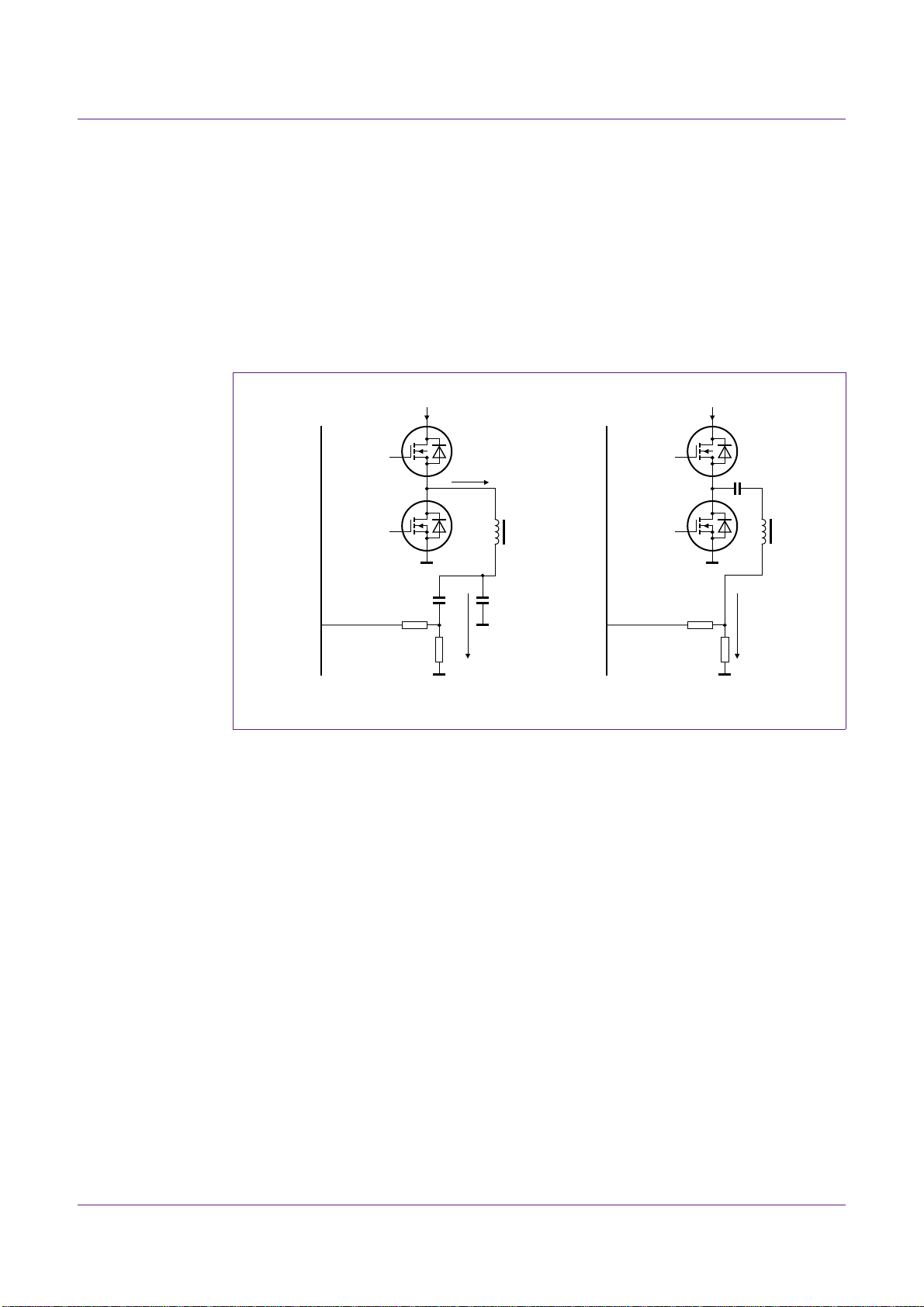
NXP Semiconductors
001aal047
V
BOOST
SNSCURHBC
I
res
17
Rcc
Rm
1 kΩ
V
BOOST
SNSCURHBC
I
res
0.02 I
res
17
Rcc
C = 1 nF
C = 49 nF
Rm
1 kΩ
The amplitude of the current depends linearly on the boost voltage. At nominal boost
voltage the current is zero and the voltage across the current sense resistor is also
present at the SNSCURHBC pin. At the boost start level SNSBOOST = 1.8 V and the
current is maximum 170 A. The direction of the current, sink or source, depends on the
active gate signal. The voltage drop created across Rcc reduces the voltage amplitude at
the pin, resulting in a higher effective current protection level. T he value of Rcc sets the
amount of compensation.
8.7.4 Current measurement circuits
AN10881
TEA1713 resonant power supply control IC with PFC
Fig 37. SNSCURHBC: resonant current measurement configurations
8.7.5 SNSCURHBC layout
Because the SNSCURHBC must be able to accurately sense the measurement signal
cycle-by-cycle at higher frequencies, it is rather susceptible to disturbances. Place the
series resistor Rcc close to the IC to reduce the length of the track that can pick up
disturbing signals. This prevents disturbances on this input. As the impedance of the
measurement resistor is normally low , the signal track between Rcc and the measurement
resistor is not critical regarding disturbance.
AN10881 All information provided in this document is subject to legal disclaimers. © NXP B.V. 2011. All rights reserved.
Application note Rev. 2 — 26 September 2011 61 of 102
Page 62

NXP Semiconductors
HYST+BURST
HB
BURST
SNSFB
HYST+BURST
HB
BURST
SNSFB
Pout
normal operation normal operationbursthold hold burst
normal operation normal operationburststop stopburst
Situation A
Situation B
001aal048
9. Burst mode operation
Burst mode operation can be used to improve the efficiency at low output loads.
By temporarily interrupting the switching, loss es duri ng idle time ar e m inim ize d. Beca us e
the average power needed for the output is low, it is easy for the converter to deliver it
during a short conversion time (a burst).
The Burst mode operation of the TEA1713 is based on interrupting the switching while
maintaining regulation. With an external comparator, the regulation voltage can be
monitored to determine if it stops switching and then continue. S topp ing and starting ag ain
can be controlled via the SNSOUT pin. When starting again af ter interruption, no sof t-start
is applied as the system is still in regulation (close to the regular working point). the
regulation-loop of the system (normally by the output voltage) determines the timing of
switching on and off. In this way, a small ripple on the output voltage is deliberately
created during Burst mode.
AN10881
TEA1713 resonant power supply control IC with PFC
Fig 38. Principle of Burst mode operation with SNSFB and comparator levels
9.1 Burst mode controlled by SNSOUT
AN10881 All information provided in this document is subject to legal disclaimers. © NXP B.V. 2011. All rights reserved.
Application note Rev. 2 — 26 September 2011 62 of 102
The HBC and the PFC of the TEA1713 can be operated in Burst mode. In Burst mode the
converters operate for a limited time, followed by a period of non-operation. Burst mode
operation increases the efficiency during low load conditions.
A simple external circuit that uses the information from the feedback loop can detect the
low load condition. The detection circuit pulls down the SNSOUT pin to pause the
operation of the TEA1713 for a burst off-time.
Page 63

NXP Semiconductors
001aal049
7.3 mA
1.5 kΩ
R
HYST
R2
R1
8 V
100 μA
1.5 V
SNSOUT
BURST
HYST
SUPREG
V
AUXILIARY
5
SNSFB21
TEA1713
OVP
latched shutdown
3.5 V
COMP
UVP
protection timer
2.35 V
COMP
HOLD HBC
1.1 V
COMP
BURST
MODE
FUNCTION
HOLD PFC
0.4 V
COMP
CONTROL
3.2 V
SNSOUT has two levels for Burst mode operation:
• Burst-off level for HBC = 1.1 V
• Burst-off level for PFC = 0.4 V
A current (100 A) from the SNSOUT pin keeps the voltage at an internal clam p voltage of
1.5 V , which is abo ve both Burst mode levels. This avoids Burst mod e activation when the
output voltage is not yet present. The impedance between the SNSOUT pin and ground
must therefore be larger than 20 k.
9.2 External comparator for Burst mode implementation
A comparator circuit between SNSFB and SNSOUT can do the implementation of the
Burst mode.
AN10881
TEA1713 resonant power supply control IC with PFC
Below this level, only the HBC pauses its operation. Both high-side and low-side
power switches are off and the PFC co ntinues full operation. Above this level the HBC
resumes operation and it does not execute a soft-start sequence.
Below this level, the PFC also pauses its operation via a soft-stop. The HBC is
already paused. Above this level the PFC resumes operation with a soft-start.
AN10881 All information provided in this document is subject to legal disclaimers. © NXP B.V. 2011. All rights reserved.
Application note Rev. 2 — 26 September 2011 63 of 102
Fig 39. Principle of Burst mode operation with SNSFB and comparator levels
Page 64

NXP Semiconductors
Pout (W)
0 504020 3010
001aal050
40
60
20
80
100
efficiency
(%)
0
with burst mode
with burst mode
normal mode
The comparator input monitors the regulation voltage SNSFB to a preset burst voltage
value by R1 and R2: BURST. When the HBC power output power is low, the regulation
voltage decreases and when it reaches BURST the switching stops by switching
SNSOUT to ground. When the switching stops, no energy is converted and the output
voltage drops. The regulation volt age then increases again. When the regulation voltage
reaches BURST + HYST (voltage hysteresis set by R
When the power delivered during a burst is larger than needed for the output, the
regulation voltage SNSFB quickly decreases, stopping the switching at BURST. The time
needed for the regulation voltage to reach BURST, is dependent on the output voltage and
its load.
When the HBC output load increases to high levels, normal operation is resumed as the
regulation voltage can no longer reach the BURST level.
9.3 Advantages of Burst mode for HBC
The main reason of applying Burst mode in a resonant converter is to improve the
efficiency at low output power by reducing the power losses.
AN10881
TEA1713 resonant power supply control IC with PFC
) the switching resumes.
HYST
The graphs in Figure 40
and Figure 41 show the improvement principle in an example of a
250 W resonant converter including (non-bursting) PFC.
Fig 40. Improved efficiency by HBC Burst mode in a 250 W converter
AN10881 All information provided in this document is subject to legal disclaimers. © NXP B.V. 2011. All rights reserved.
Application note Rev. 2 — 26 September 2011 64 of 102
Page 65

NXP Semiconductors
Pout (W)
0 15105
001aal051
8
12
4
16
20
Pin
(W)
0
with burst mode
with burst mode
normal mode
Pout (W)
0 1008040 6020
001aal052
70
80
60
90
100
efficiency
(%)
50
Fig 41. Reduced losses by HBC Burst mode in a 250 W converter
AN10881
TEA1713 resonant power supply control IC with PFC
9.4 Advantages of Burst mode for HBC and PFC simultaneously
The TEA1713 provides a Burst mode system that simultaneously switches the HBC and
PFC. In this way , durin g the burst period, the powe r is transferred directly fr om the input to
the output. The HBC determines the repetiti on time of the burst and the PFC follows. In
the burst period, the PFC operates in normal regulation.
PFC bursting obtains extra reduction in power consumption. Figure 42
examples of the results.
Fig 42. Increased efficiency at low output power in burst HBC and PFC (90 W adapter)
to Figure 44 show
AN10881 All information provided in this document is subject to legal disclaimers. © NXP B.V. 2011. All rights reserved.
Application note Rev. 2 — 26 September 2011 65 of 102
Page 66

NXP Semiconductors
Pout (W)
0 1.00.80.4 0.60.2
001aal053
1.0
1.5
0.5
2.0
2.5
Pin
(W)
0
mains = 230 VAC
mains = 100 VAC
001aal054
V
DRAIN.PFC
[100 V/div]
V
OUTPUT
[100 mV/div]
HB [100 V/div]
Fig 43. Remaining 90 W adapter losses in Burst mode
AN10881
TEA1713 resonant power supply control IC with PFC
Fig 44. Simultaneous HBC and PFC Burst mode operation (including output voltage
ripple)
9.5 Choice of burst level and hysteresis level
Set the power levels for bursting using an extern al comp arato r for dimensioning the Burst
mode. Figure 39
The basic choice for the voltage level at which the comparator must be active (BURST)
can be made experimentally.
It is important to realize that the input voltage of the resonant converter V
(see Figure 46
SNSFB regulation voltage.
shows a typical comparator circuit with hysteresis.
) influences the relationship between th e HBC outp ut power level and the
boost
AN10881 All information provided in this document is subject to legal disclaimers. © NXP B.V. 2011. All rights reserved.
Application note Rev. 2 — 26 September 2011 66 of 102
Page 67

NXP Semiconductors
Pout (W)
0 250200100 15050
001aal041
5.4
5.6
5.2
5.8
6.0
SNSFB
(V)
5.0
(1)
(2)
(3)
AN10881
TEA1713 resonant power supply control IC with PFC
1. V
2. V
3. V
BOOST
BOOST
BOOST
= 310 V (DC)
= 350 V (DC)
= 390 V (DC)
Fig 45. SNSFB voltage to output power characteristics examples
Aspects that influence the voltage levels (BURST and HYST) of Burst mode:
• Input voltage V
boost
• SNSFB voltage regulation levels in combination with the preset frequency range of
RFMAX and CFMIN
• Dynamic behavior of the regulation during Burst mode and during normal operation
(large load variations)
9.6 Output power - operating frequency characteristics
Figure 46 show that it is critical to make a design choice for a certain SNSFB voltage to
start bursting. With this kind of characteristic there is a risk that, due to spread, the system
can either remain in Burst mode or never reach Burst mode operatio n at all. The
dimensioning of the LLC can be made more suitable for Burst mode. The standard
approach is to design the system in such a wa y that it cannot regulate to no-load, even at
the highest frequency. During the lowest loads, the frequency required for regulation must
become infinite. A voltage level can then easily be chosen to ensure that Burst mode is
activated at the lowest load and that the remaining load conditions operate in Normal
mode. Burst mode now enables the system to operate at no-load.
AN10881 All information provided in this document is subject to legal disclaimers. © NXP B.V. 2011. All rights reserved.
Application note Rev. 2 — 26 September 2011 67 of 102
Page 68

NXP Semiconductors
Pout (W)
0 1008040 6020
001aal055
4.8
5.6
6.2
SNSFB
(V)
4.0
burst
level =
5 V
Pout (W)
0 1008040 6020
001aal097
120
160
200
f
(kHz)
80
AN10881
TEA1713 resonant power supply control IC with PFC
SNSFB - output power Frequency - output power
Fig 46. Normal mode output power characteristics (Adapted for easy implementation of Burst mode comparator
level detection)
9.7 Lower SUPHS in burst
During the idle time SUPHS is not charged.
During normal operation, each time the half-bridge node HB is switched to ground level,
the bootstrap function of the external diode between SUPHS and SUPREG charges the
SUPHS capacitor. In Burst mode there are periods of non-switching and therefore no
charging of SUPHS. During this time, the circuit supplied by SUPHS slowly discharges the
supply voltage capacitor. When a new burst starts, the SUPHS voltage is lower than in
normal operation. During the first switching cycles, the SUPHS is recharged to its no rmal
level. It is important that, during these first rech arge cycles, SUPREG does not drop below
the protection level of 10.3 V.
9.8 Audible noise
Because the Burst mode is normally used when the output power is low, the converted
energy does not contribute much to generate audible noise. The magnetization current
however is still present during low loads and is the dominant energy during Burst mode.
Switching the converter sequences on and off continuously at a certain speed and
duration can lead to audible noise. The main mechanism for producing noise is the
interruption of magnetization current sequences leading to a mechanical force. This is
especially the case on the core of the resonant transformer which starts acting as a
loudspeaker.
When Burst mode is applied during higher output power conditio ns, the converte d energy
also contributes and leads to an increased risk of audible noise.
9.8.1 Measurements in the resonant transformer construction
It is necessary to adapt the mechanical transfor mer construction to prevent problem s with
audible noise under specific conditions.
AN10881 All information provided in this document is subject to legal disclaimers. © NXP B.V. 2011. All rights reserved.
Application note Rev. 2 — 26 September 2011 68 of 102
Page 69

NXP Semiconductors
001aal056
One measure is to adhere the core parts to each other using a material with damping
(vibration absorbing) properties. A combination can be made with the air gap construction.
Other vibration damping measures can also help when audible noise is a critical issue for
a product.
Fig 47. Transformer construction
AN10881
TEA1713 resonant power supply control IC with PFC
(1) Left-hand transformer with glue to reduce audible noise
(2) Right-hand transformer has standard construction
9.8.2 Burst power-dependent noise level
The amount of audible noise is related to the amount of energy in each burst.
At low output power, the magnetization current of the resonant converter determines the
amount of energy. The amount of transferred energy is low. Use Burst mode only at low
power (a few watts output power) to avoid problems with audible noise. When the
transition level between Normal mode and Burst mode is chosen at a higher output powe r ,
the level of audible noise is larger.
Overshoot on feedback voltage
When the output load is increased, the system reverts to normal operation. The transition
from Burst mode to Normal mode is based on the feedback voltage. In certain burst
conditions the feedback voltage can overshoot. This keeps the system in Burst mode at
higher output power levels than intended. As the power le ve l in th is situation is larg er, the
amount of noise is also larger.
9.9 PFC converter and resonant converter simultaneous bursting
When in the Burst mode, PFC operation stops while the resonant converter is no t
switching. In most cases this saves extra energy consumption by reduced switching
losses from the PFC converter.
The behavior of the total system (PFC and resonant) in Burst mode can differ from the
situation when only the resonant converter would operate in Burst mode. Although this
results in good performance, there are a number of inter actio ns.
AN10881 All information provided in this document is subject to legal disclaimers. © NXP B.V. 2011. All rights reserved.
Application note Rev. 2 — 26 September 2011 69 of 102
Page 70

NXP Semiconductors
SNSOUT
PFC
DRAIN
HB
001aal057
9.9.1 PFC output voltage variations
When bursting the PFC converter, the resonant control system determines the timing.
This can result in a situation where the PFC cannot maintain a constant output voltage.
the HBC operation limits the time during which the PFC can convert power. This may be
too short. The result is either a lower or a varying output voltage. This also has
consequences for the resonant converter as it s input voltage is not the same. The working
conditions change towards a new balance.
The resonant converter must be able to remain operational during these conditions.
It is important to check that the resonant controller has not b een stopped because the
input voltage provided by SNSBOOST is too low. This can cause an unacceptable voltage
decrease in the output of the resonant converter.
9.9.2 PFC burst duration
Normally a square SNSOUT pulse leads to equal operation time for PFC and HBC
(see Figure 44
achieved by adding a capacitor on SNSOUT to create a ramp signal. The PFC starts at a
voltage of 0.4 V, allowing a longer PFC operating time.
AN10881
TEA1713 resonant power supply control IC with PFC
). If a longer PFC operating time is needed for correct balance, it can be
Fig 48. Example of longer burst time for PFC using ramp on SNSOUT
9.9.3 Switching between burst and normal operation
Interaction between the PFC converter and resonant converter in the Burst mode can lead
to a situation where the system alternates between Burst mode and Normal mode for
certain output power conditions.
9.9.4 Audible noise during mode transition
As a result of the previously mentioned interactions, a stable situation can occur during
the following operating modes, alternating in time:
• Resonant burst with short burst time without PFC burst (time too short to start).
• Resonant burst with long burst time and PFC burst.
• Normal operation for resonant and PFC bursts.
AN10881 All information provided in this document is subject to legal disclaimers. © NXP B.V. 2011. All rights reserved.
Application note Rev. 2 — 26 September 2011 70 of 102
Page 71

NXP Semiconductors
Transitions between modes and variation s within a certain mode have a corresponding
effect on audible noise.
9.10 Design guidelines for Burst mode operation
Design for a stable PFC (nominal) output voltage during Burst mode.
Best efficiency is achieved when the number of cycles for each burst is as small as
possible (only a few cycles).
Best efficiency is achieved by resistively tuning the comparator circuit to preset the
SNSFB burst level and hysteresis.
System and component tolerances play a sign ific an t ro le in var iations of performance in
production.
The regulation feedback loop can be optimized for Normal mode. Any additional filtering
can be done in the comparator circuit. However, use it moderately so control of the
situation can be maintained during the Burst mode operation.
AN10881
TEA1713 resonant power supply control IC with PFC
9.11 Enable/disable Burst mode
In microcontroller operated applications such as TV, a clear separation is made between
normal operation and standby operation. An enable/disable function can be added to
avoid the resonant converter entering Burst mode when short periods of low load occur
during normal operation. An extra enable/disable switch fun ction in the co mparator circuit
implements the enable/disable function.
9.12 Unused Burst mode
When the Burst mode is not required, not applying a circuit to switch SNSOUT leaves the
Burst mode function inactive.
AN10881 All information provided in this document is subject to legal disclaimers. © NXP B.V. 2011. All rights reserved.
Application note Rev. 2 — 26 September 2011 71 of 102
Page 72

NXP Semiconductors
AN10881
TEA1713 resonant power supply control IC with PFC
10. Protection functions
Most protection functions are discussed in the chapters of the systems of which they are a
part. Table 4
In the following paragraphs the remaining, more independent, protection functions are
discussed.
10.1 Protection overview
Table 4. Overview of protection functions with links
Part Symbol Protection Action Link
IC UVP-SUPIC undervoltage protection SUPIC IC disable Section 5.2.2
IC UVP-SUPREG undervoltage protection SUPREG IC disable Section 5.5
IC UVP supplies undervoltage protection supplies IC disable and reset
IC SPC-SUPIC short circuit protection SUPIC low HV start-up current Section 5.2.2
IC OVP output overvoltage protection output IC shutdown Section 10.3.1
IC UVP output Under Voltage Protection output IC restart after protection time Section 10.3.2
IC OTP overtemperature protection IC di sable Section 10.2.1
PFC OCR-PFC overcurrent regulation PFC PFC switch-off cycle-by-cycle Section 7.4
PFC UVP-mains undervoltage protection mains PFC hold switching Section 7.6.1
PFC OVP-boost overvoltage protection boost PFC hold switching Section 7.5
PFC SCP-boost short circuit protection boost IC restart Section 7.2.2
HBC UVP-boost undervoltage protection boost HBC disable Section 8.1
HBC OLP-HBC op en-loop protection HBC IC restart after protection time Section 8.5.1
HBC HFP-HBC high freque ncy pr otection HBC IC restart after protection time Section 8.4.4
HBC OCR-HBC overcurrent regulation HBC HBC frequency increase
HBC OCP-HBC overcurrent protection HBC HBC step to maximum frequency Section 8.7.2
HBC CMR Capacitive mode regulation HBC increase frequency Section 8.3.2
HBC ANO adaptive non-overlap HBC prevent hazardous switching Section 8.3.1
contains an overview of links to the corresponding places in this document.
-
Section 8.7.1
IC restart after protection time
10.2 IC protection
10.2.1 OverTemperature Protection (OTP)
The TEA1713 contains an accurate internal overtemperature protection. When the
junction temperature exceeds the overtemperature level of 140 C, the IC enters the
Thermal hold state. The Thermal hold state is left when the temperature has dropped by
10 C.
The circuit resumes operation with a complete restart including a soft-s tart of PFC and
HBC.
10.2.2 Latched protection
Only an overvoltage detection on SNSOUT leads to a latched shutdown protection state.
The voltage on SNSOUT must exceed 3.5 V to enter a latched shutdown state.
AN10881 All information provided in this document is subject to legal disclaimers. © NXP B.V. 2011. All rights reserved.
Application note Rev. 2 — 26 September 2011 72 of 102
Page 73

NXP Semiconductors
001aal058
100 μA
1.5 V
SNSOUT
SUPREG
V
AUXILIARY
5
TEA1713
OVP
latched shutdown
3.5 V
COMP
UVP
protection timer
2.35 V
COMP
HOLD HBC
1.1 V
COMP
HOLD PFC
0.4 V
COMP
Θ
10.2.2.1 Resetting a latched protection shutdown state
When a latched protection shutdown state has occurred this state is reset by one of the
following actions:
• SUPIC drops below 7 V and SUPHV is lower than 7 V
• SNSMAINS drops below 0.8 V and then rises above 0.85 V
• SSHBC/EN is pulled below 1.2 V (PFC enable level)
In most cases, a reset by the SNSMAINS voltage is activated before a reset by
SUPIC/SUPHV. This enables a restart before the V
shutdown reset).
When resetting by interrupting the mains input, some time is still required to lower the
SNSMAINS voltage below 0.8 V. The time depen ds on the component va lues used on th e
SNSMAINS circuit and the value of the mains voltage. An additional aspect is a possible
leakage of the bridge rectifiers that allows the charging of SNSMAINS by the rectified
mains voltage capacitor (reverse current through the diodes). At moderate rectifier
temperature the charging of SNSMAINSW canbe neglected but at high temperature it is a
significant parameter.
AN10881
TEA1713 resonant power supply control IC with PFC
voltage is discharged (fast
boost
A reset possibility by external control (for example microcontroller) is available using the
SSHBC/EN function.
10.3 SNSOUT protection
Fig 49. SNSOUT protection
AN10881 All information provided in this document is subject to legal disclaimers. © NXP B.V. 2011. All rights reserved.
Application note Rev. 2 — 26 September 2011 73 of 102
Page 74

NXP Semiconductors
10.3.1 OverVoltage Protection (OVP) output
The TEA1713 has an overvoltage protection intended for monitoring the HBC output
voltage. It is one of the functions that is combined on the SNSOUT pin.
10.3.1.1 Auxiliary winding
When dealing with a mains insulated converter, the HBC output voltage can be measured
via the auxiliary winding of the resonant transformer. A special transformer construction is
required to accurately measure the secondary voltage of the primary circuit auxiliary
winding.
It is important that this winding has a good coupling with the secondary winding(s) and a
minimum coupling with the primary winding . In this w ay, a good representation of the
output voltage situation is obtained (see Section 5.3.3.1
Triple insulated wire can be used to meet the mains insulation requirements.
10.3.1.2 Principle of operation
The voltage is sensed at the SNSOUT pin via an external rectifier and resistive divider.
Overvoltage is detected when the SNSOUT voltage exceeds 3.5 V. After detecting OVP
the TEA1713 enters the latched protection shutdown state.
AN10881
TEA1713 resonant power supply control IC with PFC
and Figure 7).
10.3.1.3 Connecting external measurement circuits
When latched protection is needed for other detection circuits, it can be added to
SNSOUT with a series diode.
10.3.2 UnderVoltage Protection (UVP) output
The TEA1713 has an undervoltage protection intended for monitoring the HBC output
voltage. It is one of the functions that is combined on the SNSOUT pin.
10.3.2.1 Auxiliary winding
When dealing with a mains insulated converter, the HBC output voltage can be measured
via the auxiliary winding of the resonant transformer. A special transformer construction is
required to accurately measure the secondary voltage of the primary circuit auxiliary
winding.
It is important that this winding has a good coupling with the secondary winding(s) and a
minimum coupling with the primary winding to obtain a good representation of the output
voltage situation (see Section 5.3.3.1
Triple insulated wire can be used to meet the mains insulation requirements.
10.3.2.2 Principle of operation
The voltage is sensed at the SNSOUT pin via an external rectifier and resistive divider.
Undervoltage is detected when the SNSOUT volt age drop s below 2 .35 V. When detecting
UVP the TEA1713 starts the protection timer by charging it with 100 A.
and Figure 7).
When the undervoltage state remains until the timer reaches the protection level, the
controller stops and then the restart timer restarts it.
AN10881 All information provided in this document is subject to legal disclaimers. © NXP B.V. 2011. All rights reserved.
Application note Rev. 2 — 26 September 2011 74 of 102
Page 75

NXP Semiconductors
At start-up, the SNSOUT voltage normally starts at a level lower than 2.35 V. The timer
setting must allow sufficient time for start-up to charge the SNSOUT voltage to a value
above 2.35 V, preventinfg undesired protection during start-up.
In applications where the TEA1713 is supplied from an auxiliary winding (to SUPIC), the
SUPIC monitoring can also activate a protection when an error condition results in a drop
of the output voltage (see Section 5.2.2
10.3.2.3 Severe voltage drop
When the voltage on SNSOUT drops to a low voltage, the Hold HBC and Hold PFC
functions on this input pin stop the HBC and PFC.
10.3.2.4 Connecting external measurement circuits
When restart protection is needed for other detection circuits, it can be added on
SNSOUT with a series diode.
10.3.3 OVP and UVP combinations
10.3.3.1 Circuit configurations
The following list contains examples of configurations for which certain functionality on the
SNSOUT pin is disabled.
AN10881
TEA1713 resonant power supply control IC with PFC
).
• OVP functional and UVP disabled (see Section 10.3.3.2)
• UVP functional and OVP disabled (see Section 5.3.3.3)
• Both OVP and UVP disabled (see Section 10.3.3.4)
Remark: In the examples given, Burst mode operation can still be implemented
independent of the UVP and/or OVP functionality.
10.3.3.2 OVP functional and UVP disabled
In some applications preventing the activation of the undervolt age protection on SNSOUT
by disabling UVP can be required. This can be realized by adding a circuit that prevents
the voltage on SNSOUT from dropping below 2.35 V.
As a practical example, the voltage on SNSOUT can be prevented from dropping below a
preset voltage by externally adding a low imp edance re sistive divider, with a fixed voltage
and connecting it to SNSOUT via a diode. This simple circuit is not accurate but it does
provide the basic capability to disable the UVP function of SNSOUT.
Remark: The diode is blocking for higher voltage values on SNSOUT so that the
overvoltage protection is still functional.
AN10881 All information provided in this document is subject to legal disclaimers. © NXP B.V. 2011. All rights reserved.
Application note Rev. 2 — 26 September 2011 75 of 102
Page 76
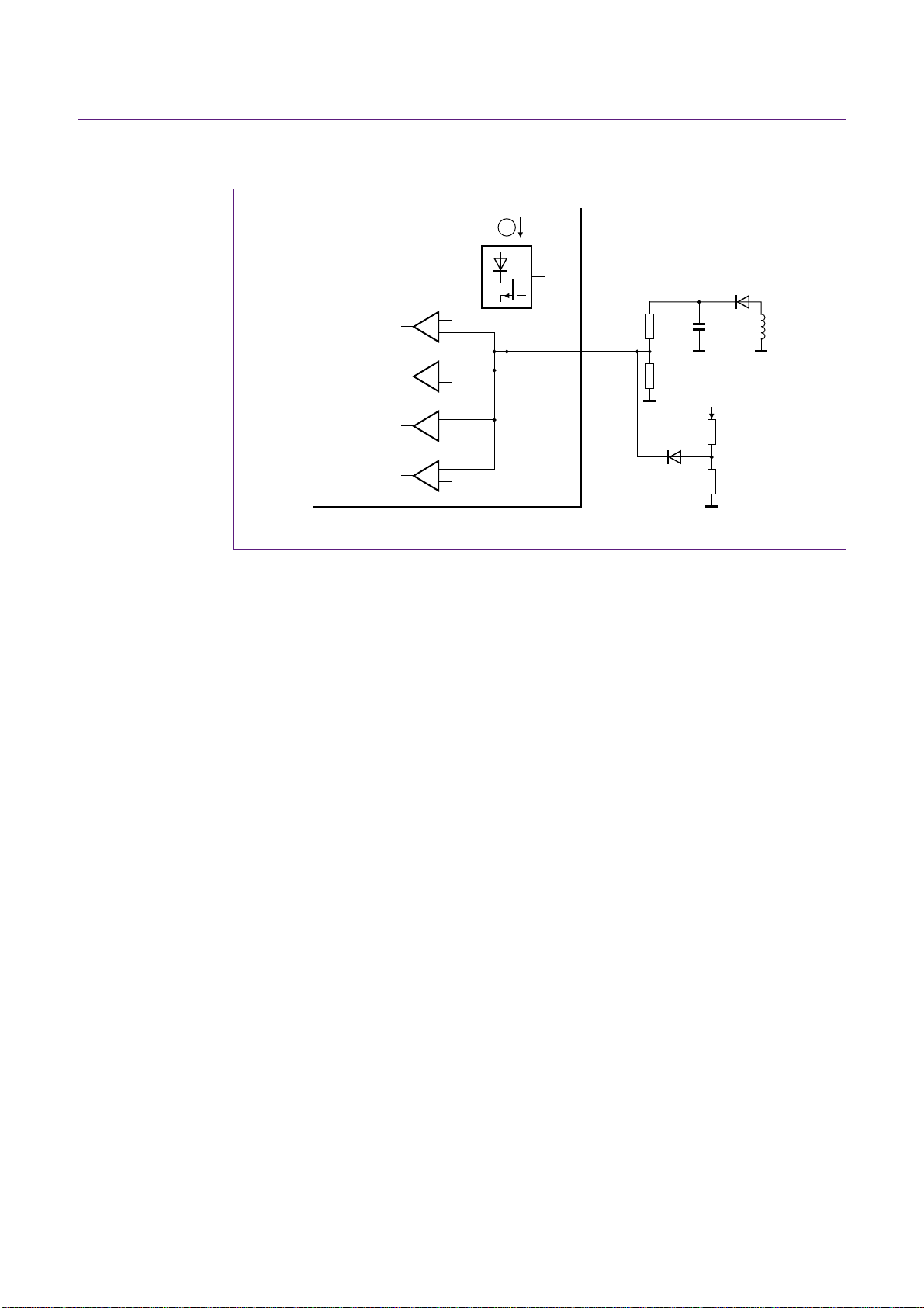
NXP Semiconductors
001aal059
100 μA
1.5 V
SNSOUT
SUPREG = 10.9 V
1N4148
8.2 kΩ
3.3 kΩ
V
AUXILIARY
5
TEA1713
OVP
latched shutdown
3.5 V
COMP
UVP
protection timer
2.35 V
COMP
HOLD HBC
1.1 V
COMP
HOLD PFC
0.4 V
COMP
Fig 50. Example of disabling the UVP function of SNSOUT
AN10881
TEA1713 resonant power supply control IC with PFC
10.3.3.3 UVP functional and OVP disabled
In some applications preventing the activa tio n of th e ove rvoltage pr ot ec tion on SNSOUT
by disabling OVP can be required. This can be realized by adding a circuit that prevents
the voltage on SNSOUT from exceeding 3.5 V.
As a practical example, the voltage on SNSOUT can be prevented from exceeding the
preset voltage by externally adding a low impedance resistive divider, with a fixed voltage,
and connecting it to SNSOUT via a diode. This simple circuit is not accurate but it does
provide the basic capability to disable the OVP function of SNSOUT.
Remark: The diode is blocking for lower voltage values on SNSOUT so that the
undervoltage protection is still functional.
Another possibility is to add a Zener diode function on SNSOUT to limit the voltage on this
pin.
AN10881 All information provided in this document is subject to legal disclaimers. © NXP B.V. 2011. All rights reserved.
Application note Rev. 2 — 26 September 2011 76 of 102
Page 77

NXP Semiconductors
001aal060
100 μA
1.5 V
SNSOUT
SUPREG = 10.9 V
1N4148
8.2 kΩ
2.7 kΩ
V
AUXILIARY
5
TEA1713
OVP
latched shutdown
3.5 V
COMP
UVP
protection timer
2.35 V
COMP
HOLD HBC
1.1 V
COMP
HOLD PFC
0.4 V
COMP
001aal061
100 μA
1.5 V
SNSOUT
SUPREG = 10.9 V
91 kΩ
33 kΩ
5
TEA1713
OVP
latched shutdown
3.5 V
COMP
UVP
protection timer
2.35 V
COMP
HOLD HBC
1.1 V
COMP
HOLD PFC
0.4 V
COMP
Fig 51. Example of disabling the OVP function of SNSOUT
AN10881
TEA1713 resonant power supply control IC with PFC
10.3.3.4 Both OVP and UVP disabled
When neither OVP or UVP functionality is required, a fixed voltage between 2.35 V and
3.5 V can be applied to SNSOUT. This can be obtained from a resistive divider that is
referenced to the SUPREG.
Fig 52. Example of disabling both the UVP and the OVP functions of SNSOUT
AN10881 All information provided in this document is subject to legal disclaimers. © NXP B.V. 2011. All rights reserved.
Application note Rev. 2 — 26 September 2011 77 of 102
Page 78
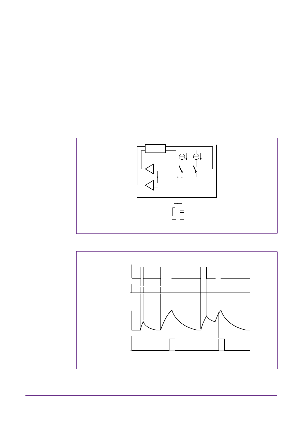
NXP Semiconductors
001aal062
RCPROT
CR
23
2 mA
100 μA
CONTROL
COMP
4 V
0.5 V
TEA1713
COMP
passed
0
0
none
present
short
error
long
error
repetitive
error
V
high(RCPROT)
I
slow(RCPROT)
I
RCPROT
Error
V
RCPROT
t
Protection time
001aal063
10.4 Protection timer
The TEA1713 has a programmable timer that is used for the timing of several forms of
protection. The timer is used in two ways:
• As a protection timer
• As a restart timer
The values for both types of timer can be independently preset by an external resistor and
capacitor connected to RCPROT.
10.4.1 Block diagram of the RCPROT function
AN10881
TEA1713 resonant power supply control IC with PFC
Fig 53. Block diagram of the RCPROT function
10.4.2 RCPROT working as protection timer
Fig 54. RCPROT protection timer operation
AN10881 All information provided in this document is subject to legal disclaimers. © NXP B.V. 2011. All rights reserved.
Application note Rev. 2 — 26 September 2011 78 of 102
Page 79

NXP Semiconductors
passed
0 V
0.5 V
no
yes
error
4 V
error
001aal064
V
RCPROT
t
restart time
Figure 54 shows the operation of the protection timer. When an error condition occurs, a
fixed current of 100 A flows from the RCPROT pin an d char g es th e ex ter n al capacitor.
The voltage rises exponentially du e to the e xterna l r esisto r. The protection time is passed
when the upper switching level of 4 V has been reached. The appropriate protective
action is then executed, the current source is stopped and the external resistor discharges
RCPROT.
If the error condition ends before 4 V has been reached, the current source is stopped and
the pin discharges through the external resistor and no further action is taken .
If the error condition is permanent, the system fluctuates between stop and restart.
The following events activate the protection timer:
• Overcurrent regulation SNSCURHBC
• High frequency protection RFMAX
• Open-loop protection SNSFB
• Undervoltage protection SNSOUT
The activation of protection (and restart) can be forced by increasing the RCPROT voltage
to above the 4 V (but no higher than 12 V) using an external circuit.
AN10881
TEA1713 resonant power supply control IC with PFC
10.4.3 RCPROT working as a restart timer
During certain error conditions, it may be desirable to temp o rarily disable the IC. This is
especially useful when an error can overheat components. A temporary disable allows
power supply components to cool down, after which the IC must automatically restart. The
restart timer determines the time to rest art.
Fig 55. RCPROT operating as a restart timer
Normally, the capacitor is discharged to 0 V but when a restart is requested, a current of
2.2 mA quickly charges the external capacitor until it reaches the upper switching level of
4 V . Af ter this, t he RCPROT pin be comes hi gh ohmic and the exte rnal resistor discharge s
the external capacitor. The restart time is exceeded when the lower switching level of
0.5 V has been reached. The IC is then restarted and the RCPROT pin is further
discharged. This condition is only activated in the case of short circuit protection of the
SNSBOOST.
AN10881 All information provided in this document is subject to legal disclaimers. © NXP B.V. 2011. All rights reserved.
Application note Rev. 2 — 26 September 2011 79 of 102
Page 80

NXP Semiconductors
t
RCPROT
t–
restart
1n
V
low RCPROT
V
high RCPROT
---------------------------------- -
----------------------------------------------- -
t–
restart
1n
0.5
4
-------
------------------- -
0.48 t
restart
===
R
V
high RCPROT
I
slow RCPROT
1e
t
protection
t
RCPROT
------------------------
–
–
------------------------------------------------------------------------------ -
4
100 A1e
t
protection
t
RCPROT
------------------------
–
–
---------------------------------------------------------------
==
C
t
RCPROT
R
--------------------
=
10.4.4 Dimensioning the timer function
AN10881
TEA1713 resonant power supply control IC with PFC
The required restart time t
determines the time constant t
restart
of R and C.
With this time constant and the required protection time t
be calculated as follows:
Example:
• t
• t
• t
=500ms
restart
protection
RCPROT
=30ms
= 240 ms
• R=341k
• C=705nF
RCPROT
protection
made by the values
(38)
, the value of R and C can
(39)
(40)
AN10881 All information provided in this document is subject to legal disclaimers. © NXP B.V. 2011. All rights reserved.
Application note Rev. 2 — 26 September 2011 80 of 102
Page 81
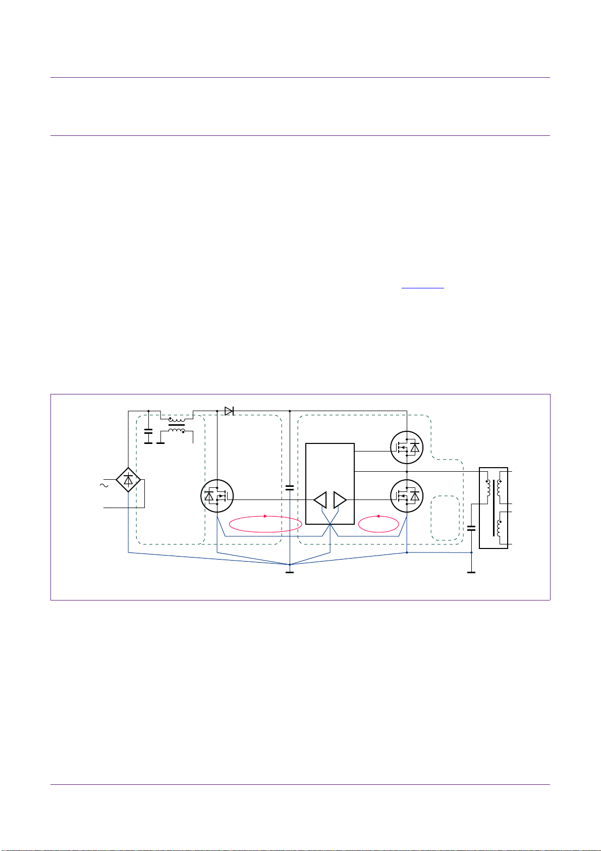
NXP Semiconductors
001aal065
TEA1713
MAINS
VOLT AGE
PFC
HBC
8
PGND
GATEPFC
GATELS
11. Miscellaneous advice and tips
1 1 .1 PCB layout
11.1.1 General setup
The TEA1713 contains two largely independent converter controllers in one package.
General advice is to physically separate the PFC and HBC circuits on the PCB to avoid
mutual interference.
11.1.2 Grounding
Connect SGND + PGND directly under the IC (on the ground plane if possible) to avoid
false signal detection by driver current disturbance (see Figure 58
A star grounding construction provides the lowest risk of mutual converter disturbance or
signal detection disturbance. In this system, the central star point can be chosen at the
capacitor ground.
V
boost
Avoid High currents on grounding tracks that are meant for signal measurement.
AN10881
TEA1713 resonant power supply control IC with PFC
).
11.1.3 Current loops
Fig 56. Grounding structure and current loops GATEPFC and GATELS
AN10881 All information provided in this document is subject to legal disclaimers. © NXP B.V. 2011. All rights reserved.
Application note Rev. 2 — 26 September 2011 81 of 102
Page 82

NXP Semiconductors
001aal066
11.1.4 Grounding layout example
AN10881
TEA1713 resonant power supply control IC with PFC
Fig 57. Grounding layout example with star point at the boost capacitor
11.1.5 Miscellaneous
11.1.5.1 Connecting SNSCURHBC (pin 17)
Place a series resistor in the SNSCURHBC connection as close as possible to pin 17.
This is important for avoiding disturbance pickup. Also avoid ca p a citive coupling between
the connection to pin 17 and the HB track (to pin 15) that contains high dV/dt signals.
11.1.5.2 CFMIN (pin 19) and RFMAX (pin 20)
Connect the oscillator capacitor on CFMIN from pin 19 to SGND pin 18 with short tracks to
prevent pickup of disturbances by an external field. Although less critical, a similar
construction can be used for RFMAX.
AN10881 All information provided in this document is subject to legal disclaimers. © NXP B.V. 2011. All rights reserved.
Application note Rev. 2 — 26 September 2011 82 of 102
Page 83

NXP Semiconductors
001aal067
1 COMPPFC
2 SNSMAINS
3 SNSAUXPFC
4 SNSCURPFC
5 SNSOUT
6 SUPIC
7 GATEPFC
8 PGND
9 SUPEG
10 GATELS
TEA1713
11 NC
12 SUPHV
RCPROT 23
SSHBC/EN 22
SNSFB 21
CFMIN 19
RFMAX 20
SNSBOOST 24
SGND 18
SNSCURHB 17
NC 16
HB 15
SUPHS 14
GATEHS 13
1 COMPPFC
2 SNSMAINS
3 SNSAUXPFC
4 SNSCURPFC
5 SNSOUT
6 SUPIC
7 GATEPFC
8 PGND
9 SUPEG
10 GATELS
TEA1713
11 NC
12 SUPHV
RCPROT 23
SSHBC/EN 22
SNSFB 21
CFMIN 19
RFMAX 20
SNSBOOST 24
SGND 18
SNSCURHB 17
NC 16
HB 15
SUPHS 14
GATEHS 13
CFMINRFMAX
Rcc C
SUPHS
AN10881
TEA1713 resonant power supply control IC with PFC
Fig 58. PCB la yout connecting SGND, PGND, CFMIN, RFMAX and SNSCURHBC
11.2 Starting/debugging partial circuits
When starting a newly built application for the first time or when an error is observed
during operation, it is possible to activate circuit parts step by step. This enables errors to
be located more easily and an evaluation can be performed under conditions that restrict
the influences from other circuit parts.
The following provides a step-by-step sequence for debugging:
1. HBC only, with protection disabled
2. HBC only, with protection disabled and variable DC input voltage
3. HBC only, with protection enabled
4. PFC only
5. PFC + HBC complete application
The best approach is to check the HBC converter first and then the PFC converter.
AN10881 All information provided in this document is subject to legal disclaimers. © NXP B.V. 2011. All rights reserved.
Application note Rev. 2 — 26 September 2011 83 of 102
Page 84

NXP Semiconductors
11.2.1 HBC only
Figure 59 shows a suggestion for the setup (temporary additions to the existing
application to force operation) and the sequence for disabling/enabling the different
functions. A moderate (current) load can be applied to the converters output to ascertain
the correct functioning.
Remark: A latching, overvoltage detection on SNSOUT (> 3.5 V), can still prevent
operation.
CFMIN, GATELS, GATEHS and HB can be monitored to continuously assess the
functioning of the converter/controller.
AN10881
TEA1713 resonant power supply control IC with PFC
When the PFC function is disabled, V
can often be applied by simply applying a DC
BOOST
or AC voltage to the mains input connections.
Check the regulation by increasing the input voltage V
for the following situations in
BOOST
the sequence given:
1. Initially at V
= 0 V: the running frequency is low with a short on-time and a long
BOOST
off-time. This is due to the HB detection not working properly at low voltage and the
internal slope detection (HB) not detecting a proper (fast) slope. In this situation a
quick check of the working of the PFC can be done by lowering the external supply
voltage of 2.7 V on SNSMAINS and SNSBOOST to a value below 2.5 V. This allows
the gate-drive pulses on GATEPFC to be seen. By varying the voltage, changes are
shown in on-time. After this check, revert the voltage to 2.7 V to continue the
HBC-only start-up (see Section 11.2.2.1
2. Increasing the value of V
at a certain input voltage the HB detection works
BOOST
).
correctly and the frequency to drive maximu m power is mini m al. If the HB s lop e
remains slow, the output current is probably low. Increasing the output current
probably results in proper HB switching.
3. When the V
input voltage has reached a level closer to the nominal working
BOOST
voltage, the correct output voltage is reached (depending on the output load), and
regulation starts working. This results in increasing the frequency with increasing the
input voltage until the nominal working voltage of V
BOOST
is set.
4. When the basic functioning of the HBC, including SNSFB regu lation, is working well,
protection can be added one by one. Proper functioning or a need for change can be
evaluated.
5. When a self-supplying application is used, the external supply voltage can be
removed when the system works well at nominal V
voltage. The system can
BOOST
now start with the internal high voltage start-up supply and an auxiliary winding can
take over the SUPIC supply.
Remark: If, during debugging or starting, a protection has been activated, switching the
SUPIC supply off and on to reset a latched protection state can be required.
AN10881 All information provided in this document is subject to legal disclaimers. © NXP B.V. 2011. All rights reserved.
Application note Rev. 2 — 26 September 2011 84 of 102
Page 85
NXP Semiconductors
001aal100
V
ext
= 25 V
DC
V
ext
= 2.7 V
DC
V
ext
= 2.7 V
DC
V
ext
= 2.7 V
DC
V
ext
= 2.7 V
DC
V
ext
= 0 V
DC
external
SUPIC
supply
enable
operation
TEA1713 by
SNSMAINS
hold PFC
operation
disable
protection
timer
disable
over current
sensing
apply nonprotection
sense voltage
(if needed)
COMPPFC
124
SNSBOOST
TEA1713
SNSMAINS
223
RCPROT
SNSAUXPFC
322
SSHBC/EN
SNSCURPFC
421
SNSFB
SNSOUT
520
RFMAX
SUPIC
619
CFMIN
GATEPFC
7 18
SGND
PGND
817
SNSCURHBC
SUPREG
916
n.c.
GATELS
10 15
HB
n.c.
11 14
SUPHS
SUPHV
12 13
GATEHS
V
ext
= 25 V
DC
V
ext
nominal
A
external
SUPIC
supply
enable
operation
TEA1713 by
SNSMAINS
hold PFC
operation
disable
protection
timer
disable
over current
sensing
apply nonprotection
sense voltage
(if needed)
COMPPFC
124
SNSBOOST
TEA1713
SNSMAINS
223
RCPROT
SNSAUXPFC
322
SSHBC/EN
SNSCURPFC
421
SNSFB
SNSOUT
520
RFMAX
SUPIC
619
CFMIN
GATEPFC
7 18
SGND
PGND
817
SNSCURHBC
SUPREG
916
n.c.
GATELS
10 15
HB
n.c.
11 14
SUPHS
SUPHV
12 13
GATEHS
V
ext
= 25 V
DC
external
SUPIC
supply
enable
operation
TEA1713 by
SNSMAINS
hold PFC
operation
disable
protection
timer
enable
over current
sensing
apply nonprotection
sense voltage
(if needed)
COMPPFC
124
SNSBOOST
TEA1713
SNSMAINS
223
RCPROT
SNSAUXPFC
322
SSHBC/EN
SNSCURPFC
421
SNSFB
SNSOUT
520
RFMAX
SUPIC
619
CFMIN
GATEPFC
718
SGND
PGND
817
SNSCURHBC
SUPREG
916
n.c.
GATELS
10 15
HB
n.c.
11 14
SUPHS
SUPHV
12 13
GATEHS
V
ext
= 25 V
DC
external
SUPIC
supply
enable
operation
TEA1713 by
SNSMAINS
hold PFC
operation
enable
protection
timer
apply nonprotection
sense voltage
(if needed)
COMPPFC
124
SNSBOOST
TEA1713
SNSMAINS
223
RCPROT
SNSAUXPFC
322
SSHBC/EN
SNSCURPFC
421
SNSFB
SNSOUT
520
RFMAX
SUPIC
619
CFMIN
GATEPFC
718
SGND
PGND
817
SNSCURHBC
SUPREG
916
n.c.
GATELS
10 15
HB
n.c.
11 14
SUPHS
SUPHV
12 13
GATEHS
B
V
ext
nominal
A
V
ext
nominal
A
enable
over current
sensing
B
C
AN10881
TEA1713 resonant power supply control IC with PFC
Fig 59. HBC only - start-up and debugging step-by-step
AN10881 All information provided in this document is subject to legal disclaimers. © NXP B.V. 2011. All rights reserved.
Application note Rev. 2 — 26 September 2011 85 of 102
Page 86

NXP Semiconductors
V
BOOST
= 100 V
HB slope is too slow for proper
detection -> High frequency
running
Increase output current -> HB slope
is fast enough for proper detection
-> Low frequency running by
"normal" SNSFB regulation
V
BOOST
= 0 V
V
BOOST
= 300 V
V
BOOST
= 40 V V
BOOST
= 60 V
V
BOOST
= 100 V
V
BOOST
= 395 VV
BOOST
= 350 V
001aal101
AN10881
TEA1713 resonant power supply control IC with PFC
Fig 60. Typical signals during a separate HBC start-up for an increase in V
The following list provides an association between pins and the protection states for which
they are being monitored:
• SSHBC/EN:
When the TEA1713 lowers the voltage to this pin, it indicates a protection with
correction to high frequency.
• RFMAX:
The voltage level on RFMAX indicates the oscillator frequency, which can cause a
high frequency protection.
• CFMIN:
A (partially) slow oscillator signal cannot observe proper detection of HB slope or a
possible Capacitive mode detection.
• PGND and SGND:
If the TEA1713 detects HB operation while there is zero inpu t voltag e, it indicates that
the connection between these pins at the IC is not p resent. Gate curre nts lead to false
HB-slope detection.
• SNSCURHBC:
Any disturbances on this pin (voltage spikes) can lead to an increase of frequency
while the original measurement voltage/signal is OK.
BOOST
AN10881 All information provided in this document is subject to legal disclaimers. © NXP B.V. 2011. All rights reserved.
Application note Rev. 2 — 26 September 2011 86 of 102
Page 87

NXP Semiconductors
001aal102
V
ext
= 25 V
DC
V
ext
= 1.5 V
DC
external
SUPIC
supply
disable
protection
timer
apply nonprotection
sense voltage
(if needed)
enable PFC and
disable HBC start
optional: remove
VBOOST connection
to high side MOSFET
COMPPFC
124
SNSBOOST
TEA1713
SNSMAINS
223
RCPROT
SNSAUXPFC
322
SSHBC/EN
SNSCURPFC
421
SNSFB
SNSOUT
520
RFMAX
SUPIC
619
CFMIN
GATEPFC
7 18
SGND
PGND
817
SNSCURHBC
SUPREG
916
n.c.
GATELS
10 15
HB
n.c.
11 14
SUPHS
SUPHV
12 13
GATEHS
• SNSOUT:
• RCPROT:
11.2.2 PFC only
Keeping SSHBC/EN below or forcing it to drop below 2.2 V can disable the HBC function.
A voltage higher than 1.2 V can enable the PFC function. Applying an additional voltage
(from an external supply) of approximately 1.5 V on SSHBC/EN enables PFC only
operation.
AN10881
TEA1713 resonant power supply control IC with PFC
The voltage on this pin must be between 2.35 V and 3.5 V for normal operation. A
voltage can be forced on pin SNSOUT to avoid p rotection . But it is often related (by a
resistive divider) to the SUPIC and is correct when SUPIC is supplied externally.
Several protection functions charges the timer.
The setup is similar to the HBC only operation setup, but for extra safety, the V
BOOST
connection to the high side switch of the HBC can be disconnected. In addition, a small
load can be connected on V
to prevent voltage overshoot and control the output
BOOST
power capability.
Fig 61. Start-up/debugging for PFC only
11.2.2.1 Operational check without mains voltage
AN10881 All information provided in this document is subject to legal disclaimers. © NXP B.V. 2011. All rights reserved.
Application note Rev. 2 — 26 September 2011 87 of 102
Without mains input voltage, by lowering the (external) voltage on SNSMAINS and
SNSBOOST to below 2.5 V, drive pulses can be observed on GATEPFC. Lower voltages
lead to a longer on-time. Below 0.89 V, pulses stop because of SNSMAINS undervoltage
protection and restarts when the level incre ases ab o ve 1. 15 V.
Page 88

NXP Semiconductors
GATEPFC GATEPFC GATEPFC
lowering the external voltage on SNSBOOST and SNSMAINS
001aal103
Fig 62. Typical GATEPFC signals without mains voltage
11.2 .2.2 Operational check with mains voltage
There is no simple step by step method of gradually increasing the mains voltage to start
PFC operation. So full mains voltage is applied to check PFC functionality. While doing
this, remove any external voltage source on SNSMAINS and SNSBOOST.
If a problem is expected of an output voltage that can be too high, the output
measurement resistor from SNSBOOST to ground can be (temporarily) increased in
value. This leads to a lower output voltage regulation setting.
AN10881
TEA1713 resonant power supply control IC with PFC
Supply a DC voltage to the mains input instead of the usual AC voltage to be able to
observe proper PFC operation more easily with an oscilloscope. This results in more
stable signals for evaluation.
11.2.3 HBC and PFC operation
When both converters work properly independently, they can be checked working
simultaneously. Remove the additions used for start-up and debugging.
Remark: A (normal) ripple voltage on V
variations in the HBC for compensation. At high output power, the voltage ripple on
V
BOOST
is larger.
results in some continuous frequency
BOOST
AN10881 All information provided in this document is subject to legal disclaimers. © NXP B.V. 2011. All rights reserved.
Application note Rev. 2 — 26 September 2011 88 of 102
Page 89

NXP Semiconductors
TEA1713 resonant power supply control IC with PFC
12. Application examples and topologies
12.1 Examples of IC evaluation and test setup
Examples of a test/evaluation setup are provided in Figure 63 and Figure 64. This setup
can be used to:
• Check if an IC is still functional (not defect).
• Evaluate specific IC function(s) or pin properties with limited interference from the
total system.
AN10881
AN10881 All information provided in this document is subject to legal disclaimers. © NXP B.V. 2011. All rights reserved.
Application note Rev. 2 — 26 September 2011 89 of 102
Page 90

NXP Semiconductors
001aal104
COMPPFC
2.5 V
regulation
124
SNSBOOST
TEA1713
SNSMAINS
SUPIC
SUPIC
223
RCPROT
SUPIC
SUPIC
SNSAUXPFC
322
SSHBC/EN
SNSCURPFC
421
SNSFB
SNSOUT
5
20
RFMAX
SUPIC
SUPIC
619
CFMIN
GATEPFC
7
18
SGND
PGND
817
SNSCURHBC
SUPREG
916
n.c.
330 nF
47 nF
47 nF
1 μF
all off
560 pF
470 pF
1 μF
1 Ω
200 Ω
2 W
200 μH
BS170
220 pF
1 kΩ
10 kΩ
200 Ω
0 Ω
4.7 kΩ
24 kΩ
1 kΩ
47 kΩ
10 kΩ
100 μH
EXT. SUPPLY
ON/OFF
EXT. SUPPLY
SUPIC
100 μF
100 μF
04N60C3
04N60C3
470 nF
560 pF
4.7 nF
4.7 μF
150 nF
BYV27-400
GATELS
10 15
HB
n.c.
n.c.
11 14
SUPHS
SUPHV
12 13
GATEHS
330 kΩ
180 kΩ
24 kΩ
2.7 kΩ
22 kΩ
56 nF
15 kΩ
470 nF 33 kΩ
2 kΩ
2.7 kΩ
22 kΩ
AN10881
TEA1713 resonant power supply control IC with PFC
Fig 63. E xample of a basic IC test setup on a single low voltage supply (24 V)
AN10881 All information provided in this document is subject to legal disclaimers. © NXP B.V. 2011. All rights reserved.
Application note Rev. 2 — 26 September 2011 90 of 102
Page 91

Application note Rev. 2 — 26 September 2011 91 of 102
001aal105
HALF BRIDGE PART
PFC PART
SUPPLY PART
MAINS RESET
UNDER-VOLTAGE
SENSING AND CLAMP
+1.12 V
+2.5 V
PFC driver
SupReg
Low-side driver
SupReg
PGND
error
amplifier
and clamp
TEA1713
MAINS
COMPENSATION
DEMAGNETIZING
SENSING
−0.1 V
VALLEY
SENSING
SOFT START
CONTROL
+0.495 V
+0.5 V
+2 V
+1 V
+2.63 V
OVER-CURRENT
SENSING
+3.0 V
SOFTSTART
RESET
+8.0 V
8 V
4.5 V
POLARITY
INVERSION
FEEDBACK
INPUT
7.6 V
OPEN LOOP
SENSING
+1.88 V
HIGH
FREQUENCY
SENSING
CONTROLLED
OSCILATOR
I-V
+
V-I
BOOST
OVER-VOLTAGE
SENSING
RESTART AND
PROTECTION
TIMER
OVER-
TEMPERATURE
SENSING
ENABLE SENSING
PFC/
HALF BRIDGE
1.0 V
+0.4 V
BURST SENSING
PFC/HBC
+3.5 V
OUTPUT
OVER-VOLTAGE
SENSING
+1 V
−1 V
OVER-CURRENT
PROTECTION
SENSING
CAPACITIVE
MODE
SENSING
ADAPTIVE
NON-OVERLAP
SENSING
SWITCH
CONTROL
LEVEL
SHIFTER
+2.3 V
OUTPUT
UNDER-VOLTAGE
SENSING
+0.5 V
−0.5 V
OVER-CURRENT
REGULATION
SENSING
+8.0 V
+3.0 V
+6.0 V
TWO SPEED
SOFTSTART SWEEP
AND CLAMP
BOOST
COMPENSATION
+11 V
6
SUPIC
12
SUPHV
9
SUPREG
24
SNSBOOST
+10.3 V
SERIES
STABILIZER AND
SUPREG SENSING
+22/17 V
+15 V
+20 V
SUPIC START
AND
UNDER-VOLTAGE
SENSING
SUPPLY
CONTROL
INTERNAL
SUPPLIES
HV START-UP
SELECTION
HV START-UP
SOURCE
+1.72 V
BOOST
UNDER-VOLTAGE
SENSING
+0.4 V
BOOST
SHORT
SENSING
ON-TIMER
OFF-TIME LIMIT
FREQUENCY LIMIT
PFC
CONTROL
FREQUENCY
CONTROL
High-side driver 14 SUPHS
SNSMAINS 2
COMPPFC 1
GATEPFC 7
SNSAUXPFC 3
SNSCURPFC 4
RCPROT
2.2 μF
110 kΩ
120 kΩ
10 kΩ
1 kΩ
10 kΩ
10 kΩ
47 kΩ
33 kΩ
100 kΩ
47 nF
680 pF
1 nF
100 nF
100 nF
40 V
1N4937
600 V
100 nF
0 Ω
0 Ω
15 kΩ
2 kΩ
1 Ω
10 Ω
0.1 W
6NK60
1 Ω/600 V
100 pF
600 V
optional
100 pF
10 nF
10 nF
220 nF
180 pF
4.3 V 10 V
BS170
4.7 kΩ 100 kΩ
10 nF
600 V
100 nF
600 V
3.3 mH
10 nF
600 V
100 μF
40 V
BS170
2N7000
BS170
1N4148
1N4148
1N4148
SupplyLv (33 V)
1N4148
25 V
3.3 mH
27 nF
2.7 nF
10 nF
15 kΩ
18 kΩ
82 kΩ
1 μF
12 V
15 kΩ
27 kΩ
82 kΩ
8.2 kΩ
1 Ω
1.5 Ω
100 nF18 kΩ
68 kΩ
23
13 GATEHS
15 HB
10 GATELS
8 PGND
CENTRAL
GROUND
GND
SupplyHv (400 V)
17 SNSCURHBC
5 SNSOUT
RestartNot
11 V: operating
0 V for > 150 ms: restart
21
19
CFMIN20RFMAX
22
SSHBC/EN
SupReg
OPERATION OK
18
SGND
SNSFB
xxxxxxxxxxxxxxxxxxxxx xxxxxxxxxxxxxxxxxxxxxxxxxx xxxxxxx x x x xxxxxxxxxxxxxxxxxxxxxxxxxxxxxx xxxxxxxxxxxxxxxxxxx xx xx xxxxx
xxxxxxxxxxxxxxxxxxxxxxxxxxx xxxxxxxxxxxxxxxxxxx xxxxxx xxxxxxxxxxxxxxxxxxxxxxxxxxxxxxxxxxx xxxxxxxxxxxx x x
xxxxxxxxxxxxxxxxxxxxx xxxxxxxxxxxxxxxxxxxxxxxxxxxxxx xxxxx xxxxxxxxxxxxxxxxxxxxxxxxxxxxxxxxxxxxxxxxxxxxxxxxxx xxxxxxxx
AN10881 All information provided in this document is subject to legal disclaimers. © NXP B.V. 2011. All rights reserved.
xxxxxxxxxxxxxxxxxxxxxxxxx xxxxxxxxxxxxxxxxxxxx xxx
NXP Semiconductors
Fig 64. Example of a basic IC evaluation and test setup with a high bus voltage
TEA1713 resonant power supply control IC with PFC
AN10881
Page 92
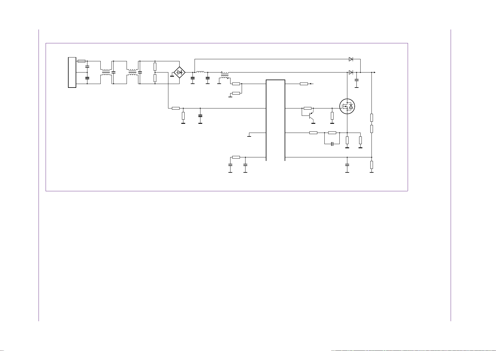
Application note Rev. 2 — 26 September 2011 92 of 102
001aal106
L
G
F101
CN101
L101
C102
2.2 nF
C103
0.22 μF
C111
0.22 μF
R101
2 MΩ
R104
47 kΩ
R110
100 kΩ
R105
0.1 Ω
1W
R114
58.2 kΩ
R113
4.7 MΩ
R112
4.7 MΩ
R106
0.1 Ω
1W
Q201
PBSS5350T
Q101
K3934
R103
5.1 kΩ
IC101
3.6 kΩ
SNSAUXPFC
3
SNSMAINS
2
PGND
8
COMPPFC
SUPHV
VBUS
VBUS
GATEPFC
SNSCURPFC
SNSBOOST
1
12
7
4
24
BD101
GBU6K
D101
1N5408
D102
BYV29X-600
R108
33 kΩ
R119
0 Ω
R111
10 Ω
R115
2.2 kΩ
R107
12 kΩ
R102
2 MΩ
R116
560 kΩ
C101
2.2 nF
C107
47 nF
C112
1 μF
C112
1 μF
C106
470 nF
C105
150 nF
C109
10 nF
C110
220 μF
420 V
C114
1 μF
L104
220 μH
L103
200 μH
N
TEA1713
L102
xxxxxxxxxxxxxxxxxxxxx xxxxxxxxxxxxxxxxxxxxxxxxxx xxxxxxx x x x xxxxxxxxxxxxxxxxxxxxxxxxxxxxxx xxxxxxxxxxxxxxxxxxx xx xx xxxxx
xxxxxxxxxxxxxxxxxxxxxxxxxxx xxxxxxxxxxxxxxxxxxx xxxxxx xxxxxxxxxxxxxxxxxxxxxxxxxxxxxxxxxxx xxxxxxxxxxxx x x
xxxxxxxxxxxxxxxxxxxxx xxxxxxxxxxxxxxxxxxxxxxxxxxxxxx xxxxx xxxxxxxxxxxxxxxxxxxxxxxxxxxxxxxxxxxxxxxxxxxxxxxxxx xxxxxxxx
AN10881 All information provided in this document is subject to legal disclaimers. © NXP B.V. 2011. All rights reserved.
xxxxxxxxxxxxxxxxxxxxxxxxx xxxxxxxxxxxxxxxxxxxx xxx
12.2 Example of a 250 W LCD TV application
NXP Semiconductors
TEA1713 resonant power supply control IC with PFC
Fig 65. Example of a 250 W LCD TV application (part 1 of 3)
AN10881
Page 93

Application note Rev. 2 — 26 September 2011 93 of 102
001aal107
C312
330 nF
C311
4.7 nF
C326
3.3 μF
C322
2 μF
C308
680 nF
C310
47 nF
C313
1 mF
C318
2.7 nF
C309
1 nF
C302
220 pF
C301
220 pF
C306
680 nF
C321
10 nF
C365
150 nF
C360
150 nF
C361
10 nF
C362
3.3 nF
IC102A
LM393
IC302
SFH615
IC303
TL431
IC102B
LM393
C300
4.7 μF
C304
100 μF
C307
10 μF
R302
150 kΩ
D312
R303
C305
330 pF
27 kΩ
R352
10 Ω
R365
270 kΩ
R117
D366
BAS316
D306
48CTQ060
D305
48CTQ060
D366
BAS316
1.5 Ω
R315
470 Ω
C323
47 nF
R323
2.7 kΩ
R363
91 kΩ
R352
1N4148
D351
T1
LP3925
Lp = 660 μH
Ls = 110 μH
34:4:4:2:2:4
R353
100 kΩ
R366
39 kΩ
R310
4.7 Ω
R361
68 kΩ
R360
33 kΩ
R367
2.2 kΩ
R317
100 Ω
R313
1 kΩ
R312
36 kΩ
R314
10 kΩ
R368
0 Ω
R369
n.c.
R364
n.c.
R362
33 kΩ
51 Ω
R301
2 kΩ
1N4007
GATEHS SUPHV
13 12
SUPHS
SUPREG
SUPREG
SUPREG
SUPREG
n.c.
14 11
HB GATELS
15 10
n.c. SUPREG
SUPREG
SUPIC
SNSCURHB
VBUS
16 9
SNSCURHBC
SNSCURHBC
PGND
17 8
SGND GATEPFC
18 7
CFMIN SUPIC
19 6
2
3
4
6
5
1
8
7
RFMAX SNSOUT
20 5
SNSFB SNSCURPFC
21 4
SSHBC/EN
EN
SNSAUXPFC
22 3
RCPROT SNSMAINS
23 2
SNSBOOST COMPPFC
24 1
TEA1713
IC101
C319
1 mF
C314
1 mF
C315
1 mF
C316
1 mF
C317
1 mF
L301
1 μH
C320
1 mF
C325
2.2 nF
C324
n.c.
R355
10 Ω
R356
1N4148
D355
R357
100 kΩ
Q302
12N50C3
Q307
BC847-40
Q301
12N50C3
51 Ω
(1)
D304
SBL2060CT
D303
SBL2060CT
L302
1 μH
24 V_8 A
12 V_4 A
xxxxxxxxxxxxxxxxxxxxx xxxxxxxxxxxxxxxxxxxxxxxxxx xxxxxxx x x x xxxxxxxxxxxxxxxxxxxxxxxxxxxxxx xxxxxxxxxxxxxxxxxxx xx xx xxxxx
xxxxxxxxxxxxxxxxxxxxxxxxxxx xxxxxxxxxxxxxxxxxxx xxxxxx xxxxxxxxxxxxxxxxxxxxxxxxxxxxxxxxxxx xxxxxxxxxxxx x x
xxxxxxxxxxxxxxxxxxxxx xxxxxxxxxxxxxxxxxxxxxxxxxxxxxx xxxxx xxxxxxxxxxxxxxxxxxxxxxxxxxxxxxxxxxxxxxxxxxxxxxxxxx xxxxxxxx
AN10881 All information provided in this document is subject to legal disclaimers. © NXP B.V. 2011. All rights reserved.
xxxxxxxxxxxxxxxxxxxxxxxxx xxxxxxxxxxxxxxxxxxxx xxx
NXP Semiconductors
Fig 66. Example of a 250 W LCD TV application (part 2 of 3)
(1) Remove to enable Burst mode operation
TEA1713 resonant power supply control IC with PFC
AN10881
Page 94

Application note Rev. 2 — 26 September 2011 94 of 102
001aal108
R217
1 Ω
R204
75 kΩ
C401
2.2 nF
IC202
SFH615
R206
5.1 kΩ
R237
12 kΩ
C206
10 nF
C202
47 μF
R201
2.7 MΩ
R203
4.7 Ω
R208
100 Ω
R215
1.5 kΩ
R218
10 kΩ
R219
10 kΩ
R320
91 Ω
R213
5.1 kΩ
C209
470 μF
C210
470 μF
C211
470 μF
5 V_2A
L201
R118
n.c.
R216
n.c.
IC203
TL341
C213
47 nF
C212
C201
2.2 nF
C208
1.5 nF
D201
1N4007
D204
48CTQ060
D202
1N4148
ZD201
30 V
IC201
C215
220
pF
1
VCC
VCC
VCC
SUPIC
VBUS
2
GND
3
RC
4
REG
8
DRAIN
TEA1523
T201
7
n.c.
6
SOURCE
5
AUX
22 nF
IC304
SFH610
EN
5 V
S1
STBY
xxxxxxxxxxxxxxxxxxxxx xxxxxxxxxxxxxxxxxxxxxxxxxx xxxxxxx x x x xxxxxxxxxxxxxxxxxxxxxxxxxxxxxx xxxxxxxxxxxxxxxxxxx xx xx xxxxx
xxxxxxxxxxxxxxxxxxxxxxxxxxx xxxxxxxxxxxxxxxxxxx xxxxxx xxxxxxxxxxxxxxxxxxxxxxxxxxxxxxxxxxx xxxxxxxxxxxx x x
xxxxxxxxxxxxxxxxxxxxx xxxxxxxxxxxxxxxxxxxxxxxxxxxxxx xxxxx xxxxxxxxxxxxxxxxxxxxxxxxxxxxxxxxxxxxxxxxxxxxxxxxxx xxxxxxxx
AN10881 All information provided in this document is subject to legal disclaimers. © NXP B.V. 2011. All rights reserved.
xxxxxxxxxxxxxxxxxxxxxxxxx xxxxxxxxxxxxxxxxxxxx xxx
NXP Semiconductors
Fig 67. Example of a 250 W LCD TV application (part 3 of 3)
TEA1713 resonant power supply control IC with PFC
AN10881
Page 95

Application note Rev. 2 — 26 September 2011 95 of 102
001aal109
L
G
F101
CN101
L102
C102
2.2 nF
C103
0.47 μF
C111
0.47 μF
R101
2 MΩ
R104
47 kΩ
R110
100 kΩ
R2
0.1 Ω
1W
R114
60 kΩ
R113
4.7 MΩ
R112
4.7 MΩ
Q201
PBSS5350T
Q101
K3934
R103
5.1 kΩ
IC101
3.6 kΩ
SNSAUXPFC
3
SNSMAINS
2
PGND
8
COMPPFC
SUPHV
VBUS
VBUS
GATEPFC
SNSCURPFC
SNSBOOST
1
12
7
4
24
BD101
GBU6K
D101
1N5408
D102
BYV29X-600
R108
33 kΩ
R119
0 Ω
R111
10 Ω
R115
2.2 kΩ
R107
12 kΩ
R102
2 MΩ
R116
560 kΩ
C101
2.2 nF
C107
47 nF
C112
470 nF
C113
3.3 μF
C106
470 nF
C105
150 nF
C109
10 nF
C110
47 μF
420 V
C114
470 nF
L104
220 μH
L103
(1)
250 μH
N
TEA1713
xxxxxxxxxxxxxxxxxxxxx xxxxxxxxxxxxxxxxxxxxxxxxxx xxxxxxx x x x xxxxxxxxxxxxxxxxxxxxxxxxxxxxxx xxxxxxxxxxxxxxxxxxx xx xx xxxxx
xxxxxxxxxxxxxxxxxxxxxxxxxxx xxxxxxxxxxxxxxxxxxx xxxxxx xxxxxxxxxxxxxxxxxxxxxxxxxxxxxxxxxxx xxxxxxxxxxxx x x
xxxxxxxxxxxxxxxxxxxxx xxxxxxxxxxxxxxxxxxxxxxxxxxxxxx xxxxx xxxxxxxxxxxxxxxxxxxxxxxxxxxxxxxxxxxxxxxxxxxxxxxxxx xxxxxxxx
AN10881 All information provided in this document is subject to legal disclaimers. © NXP B.V. 2011. All rights reserved.
xxxxxxxxxxxxxxxxxxxxxxxxx xxxxxxxxxxxxxxxxxxxx xxx
12.3 Example of a 90 W notebook adapter application
NXP Semiconductors
TEA1713 resonant power supply control IC with PFC
Fig 68. Example of a 90 W notebook adapter application (part 1 of 2)
AN10881
Page 96

Application note Rev. 2 — 26 September 2011 96 of 102
001aal110
C312
330 nF
C311
4.7 nF
C326
3.3 μF
C322
2 μF
C308
680 nF
C310
22 nF
C318
2.7 nF
C309
1 nF
C302
220 pF
C301
220 pF
C306
680 nF
C321
10 nF
C365
150 nF
C360
150 nF
C361
10 nF
C362
3.3 nF
IC102A
LM393
IC302
SFH615
IC303
TL431
IC102B
LM393
C300
4.7 μF
C304
100 μF
C307
10 μF
R302
150 kΩ
D312
R303
C305
330 pF
27 kΩ
R352
10 Ω
R365
270 kΩ
R117
D366
BAS316
D306
48CTQ060
D305
48CTQ060
D366
BAS316
1.5 Ω
R315
470 Ω
C323
47 nF
R323
2.7 kΩ
R363
91 kΩ
R352
1N4148
D351
T1
R353
100 kΩ
R366
39 kΩ
R310
4.7 Ω
R361
68 kΩ
R360
33 kΩ
R367
2.2 kΩ
R317
100 Ω
R313
5.1 kΩ
R312
36 kΩ
R368
0 Ω
R369
n.c.
R364
n.c.
R362
33 kΩ
51 Ω
R301
2 kΩ
1N4007
GATEHS SUPHV
13 12
SUPHS
SUPREG
SUPREG
SUPREG
SUPREG
n.c.
14 11
HB GATELS
15 10
n.c. SUPREG
SUPREG
SUPIC
SNSCURHB
VBUS
16 9
SNSCURHBC
SNSCURHBC
PGND
17 8
SGND GATEPFC
18 7
CFMIN SUPIC
19 6
2
3
4
6
5
1
8
7
RFMAX SNSOUT
20 5
SNSFB SNSCURPFC
21 4
SSHBC/EN
EN
SNSAUXPFC
22 3
RCPROT SNSMAINS
23 2
SNSBOOST COMPPFC
24 1
TEA1713
IC101
C319
470 μF
C320
470 μF
C325
2.2 nF
C324
n.c.
R355
10 Ω
R356
1N4148
D355
R357
100 kΩ
Q302
04N60C3
Q307
BC847-40
Q301
04N60C3
51 Ω
L302
1 μH
C401
2.2 nF
20 V_4.5 A
Lp ≈ 820 μH
Ls ≈ 220 μH
60 : 6 : 6 : 7
xxxxxxxxxxxxxxxxxxxxx xxxxxxxxxxxxxxxxxxxxxxxxxx xxxxxxx x x x xxxxxxxxxxxxxxxxxxxxxxxxxxxxxx xxxxxxxxxxxxxxxxxxx xx xx xxxxx
xxxxxxxxxxxxxxxxxxxxxxxxxxx xxxxxxxxxxxxxxxxxxx xxxxxx xxxxxxxxxxxxxxxxxxxxxxxxxxxxxxxxxxx xxxxxxxxxxxx x x
xxxxxxxxxxxxxxxxxxxxx xxxxxxxxxxxxxxxxxxxxxxxxxxxxxx xxxxx xxxxxxxxxxxxxxxxxxxxxxxxxxxxxxxxxxxxxxxxxxxxxxxxxx xxxxxxxx
AN10881 All information provided in this document is subject to legal disclaimers. © NXP B.V. 2011. All rights reserved.
xxxxxxxxxxxxxxxxxxxxxxxxx xxxxxxxxxxxxxxxxxxxx xxx
NXP Semiconductors
Fig 69. Example of a 90 W notebook adapter application (part 2 of 2)
TEA1713 resonant power supply control IC with PFC
AN10881
Page 97

NXP Semiconductors
TEA1713 resonant power supply control IC with PFC
13. Differences between TEA1713T and TEA1713LT
It is often required for stand-alone, single output power supplies like adapters, to have an
extended amount of protections leading to a latched protection instead of a safe restart.
For this reason the TEA1713LT product version was derived from the TEA1713T.
The functional differences in the TEA1713LT are:
• SNSOUT UVP (pin 5):
In the TEA1713LT the UVP function on pin SNSOUT is disabled because the function
is often not required. Disabling the UVP function provides more design flexibility and
prevent false triggering.
• SNSFB OLP-HBC (pin 21):
In the TEA1713LT the open-loop protection on SNSFB leads to a latched protection
after the protection timer (RCPROT) has triggered the protection. In the TEA1713T
the system continues with a safe restart.
• RFMAX HFP-HBC (pin 20):
In the TEA1713LT the high frequency protection on RFMAX leads to a latched
protection after the protection timer (RCPROT) has triggered the protection. In the
TEA1713T the system continues with a safe restart.
• SNSCURHBC OCR-HBC (pin 17):
In the TEA1713LT the overcurrent regulation on SNSCURHBC leads to a latched
protection after the protection timer (RCPROT) has triggered the protection. In the
TEA1713T the system continues with a safe restart.
The OCP increases the frequency during the period until the protection timer is
finished. This procedure is the same for TEA1713LT and TEA1713T
• SNSCURHBC OCP-HBC (pin 17):
In the TEA1713LT version the overcurrent protection function on SNSCURHBC is
disabled because the OCR is a latched protection. Disabling the OCP function
provides more design flexibility and prevents false triggering.
AN10881
AN10881 All information provided in this document is subject to legal disclaimers. © NXP B.V. 2011. All rights reserved.
Application note Rev. 2 — 26 September 2011 97 of 102
Page 98

NXP Semiconductors
14. Abbreviations
Table 5. Abbreviations
Acronym Description
ADT Adaptive Dead Time
BCD Bipolar CMOS DMOS
CMR Common Mode Rejection
EMC ElectroMagnetic Compatibility
EMI ElectroMagnetic Interference (or Immunity)
HB Half-Bridge
HBC Half-Bridge Converte r (or Control ler)
HFP High-Frequency Protection
HV High-Voltage
IC Integrated Circuit
LCD Liquid Crystal Display
LLC Resonant tank or Converter (Lm + Lr + Cr in series)
OCP OverCurrent Protection
OCR OverCurrent Regulation
OLP Open-Loop Protection
OPTO Opto coupler
OTP OverTemperature Protection
OVP OverVoltage Protection
PCB Printed-Circuit Board
PFC Power Factor Converter/Controller/Correction
PWM Pulse Width Modulation
SCP Short Circuit Protection
SOI Silicon-On-Insulator
UVP UnderVoltage Protection
AN10881
TEA1713 resonant power supply control IC with PFC
AN10881 All information provided in this document is subject to legal disclaimers. © NXP B.V. 2011. All rights reserved.
Application note Rev. 2 — 26 September 2011 98 of 102
Page 99

NXP Semiconductors
15. Legal information
AN10881
TEA1713 resonant power supply control IC with PFC
15.1 Definitions
Draft — The document is a draft version only. The content is still under
internal review and subject to formal approval, which may result in
modifications or additions. NXP Semiconductors does not give any
representations or warranties as to the accuracy or completeness of
information included herein and shall have no liability for the consequences of
use of such information.
15.2 Disclaimers
Limited warranty and liability — Information in this document is believed to
be accurate and reliable. However, NXP Semiconductors does not give any
representations or warranties, expressed or implied, as to the accuracy or
completeness of such information and shall have no liability for the
consequences of use of such information.
In no event shall NXP Semiconductors be liable for any indirect, incidental,
punitive, special or consequential damages (including - without limitation - lost
profits, lost savings, business interruption, costs related to the removal or
replacement of any products or rework charges) whether or not such
damages are based on tort (including negligence), warranty, breach of
contract or any other legal theory.
Notwithstanding any damages that customer might incur for any reason
whatsoever, NXP Semi conductors’ aggregat e and cumulative liabil ity towards
customer for the products described herein shall be limited in accordance
with the Terms and conditions of commercial sale of NXP Semiconductors.
Right to make changes — NXP Semiconductors reserves the right to make
changes to information published in this document, including without
limitation specifications and product descriptions, at any time and without
notice. This document supersedes and replaces all information supplied prior
to the publication hereof.
Suitability for use — NXP Semiconductors products are not designed,
authorized or warranted to be suitable for use in life support, life-critical or
safety-critical systems or equipment, nor in applications where failure or
malfunction of an NXP Semiconductors product can reasonably be expected
to result in personal injury, death or severe property or environmental
damage. NXP Semiconductors accepts no liability for inclusion and/or use of
NXP Semiconductors products in such equipment or applica tions and
therefore such inclusion and/or use is at the customer’s own risk.
Applications — Applications that are described herein for any of these
products are for illustrative purposes only. NXP Semiconduct ors makes no
representation or warranty that such applications will be suitable for the
specified use without further testing or modification.
Customers are responsible for the design and operation of their applications
and products using NXP Semiconductors product s, and NXP Semiconductors
accepts no liability for any assistance with applications or customer product
design. It is customer’s sole responsibility to determine whether the NXP
Semiconductors product is suitable and fit for the customer’s applications and
products planned, as well as for the planned application and use of
customer’s third party customer(s). Customers should provide appropriate
design and operating safeguards to minimize the risks associated with their
applications and products.
NXP Semiconductors does not accept any liability related to any default ,
damage, costs or problem which is based on any weakness or default in the
customer’s applications or products, or the application or use by customer’s
third party customer(s). Customer is responsible for doing all necessary
testing for the customer’s applications and products using NXP
Semiconductors products in order to avoid a default of the applications and
the products or of the application or use by customer’s third part y
customer(s). NXP does not accept any liability in this respect.
Export control — This document as well as the item(s) described herein
may be subject to export control regulations. Export might require a prior
authorization from competent authorities.
Evaluation products — This product is provided on an “as is” and “with all
faults” basis for evaluation purposes only. NXP Semiconductors, its affiliates
and their suppliers expressly disclaim all warranties, whet her express, implied
or statutory, including but not limited to the implied warranties of
non-infringement, merchantability and fitness for a particular purpose. The
entire risk as to the quality, or arising out of the use or performance, of this
product remains with customer.
In no event shall NXP Semiconductors, its affiliates or their su ppliers be liable
to customer for any special, indirect, consequential, punitive or incidental
damages (including without limitation damages for l oss of bu siness, busi ness
interruption, loss of use, loss of data or information, and the like) arising out
the use of or inability to use the product, whether or not based on tort
(including negligence), strict liability, breach of contract, breach of warranty or
any other theory , even if advised of the possibility of such damages.
Notwithstanding any damages that customer might incur for any reason
whatsoever (including without limitation, all damages referenced above and
all direct or general damages), the entire liability of NXP Semiconductors, its
affiliates and their suppliers and customer’s exclusive remedy for all of the
foregoing shall be limited to actual damages incurred by customer based on
reasonable reliance up to the greater of the amount actually paid by customer
for the product or five dollars (US$5.00). The foregoin g limita tions, exclusions
and disclaimers shall apply to the maximum extent permitted by applicable
law, even if any remedy fails of its essential purpose.
15.3 Trademarks
Notice: All referenced brands, prod uct names, service names and trademarks
are the property of their respective owners.
AN10881 All information provided in this document is subject to legal disclaimers. © NXP B.V. 2011. All rights reserved.
Application note Rev. 2 — 26 September 2011 99 of 102
Page 100

NXP Semiconductors
16. Contents
AN10881
TEA1713 resonant power supply control IC with PFC
1 Introduction . . . . . . . . . . . . . . . . . . . . . . . . . . . . 3
1.1 Scope and setup. . . . . . . . . . . . . . . . . . . . . . . . 3
1.2 Related documents. . . . . . . . . . . . . . . . . . . . . . 4
2 TEA1713 highlights and features. . . . . . . . . . . 5
2.1 Resonant conversion . . . . . . . . . . . . . . . . . . . . 5
2.2 Power factor correction conversion . . . . . . . . . 5
2.3 TEA1713 resonant power supply control IC
with PFC. . . . . . . . . . . . . . . . . . . . . . . . . . . . . . 6
2.4 Features . . . . . . . . . . . . . . . . . . . . . . . . . . . . . . 6
2.4.1 General features. . . . . . . . . . . . . . . . . . . . . . . . 6
2.4.2 Power factor controller features . . . . . . . . . . . . 7
2.4.3 Resonant half-bridge controller features. . . . . . 7
2.4.4 Protection features. . . . . . . . . . . . . . . . . . . . . . 7
2.5 Protection . . . . . . . . . . . . . . . . . . . . . . . . . . . . . 7
2.6 Typical areas of application . . . . . . . . . . . . . . . 7
3 Pin overview with functional description . . . . 8
4 Application diagram and block diagrams . . . 12
5 Supply functions . . . . . . . . . . . . . . . . . . . . . . . 16
5.1 Basic supply system overview . . . . . . . . . . . . 16
5.1.1 TEA1713 supplies . . . . . . . . . . . . . . . . . . . . . 16
5.1.2 Supply monitoring and protection. . . . . . . . . . 17
5.2 SUPIC - the low voltage IC supply . . . . . . . . . 17
5.2.1 SUPIC start-up . . . . . . . . . . . . . . . . . . . . . . . . 17
5.2.1.1 SUPHV 25 V
5.2.1.2 SUPHV not connected/used. . . . . . . . . . . . . . 17
5.2.2 SUPIC stop, UVP and SCP . . . . . . . . . . . . . . 17
5.2.3 SUPIC current consumption. . . . . . . . . . . . . . 18
5.3 SUPIC supply using HBC transformer auxiliary
winding . . . . . . . . . . . . . . . . . . . . . . . . . . . . . . 18
5.3.1 Start-up by SUPHV. . . . . . . . . . . . . . . . . . . . . 18
5.3.2 Block diagram for SUPIC start-up. . . . . . . . . . 19
5.3.3 Auxiliary winding on the HBC transformer . . . 19
5.3.3.1 SUPIC and SNSOUT by auxiliary winding . . . 20
5.3.3.2 Auxiliary supply voltage variations by output
current . . . . . . . . . . . . . . . . . . . . . . . . . . . . . . 20
5.3.3.3 Voltage variations by auxiliary winding
position: primary side component. . . . . . . . . . 20
5.3.4 Difference between UVP on SNSOUT and
SNSCURHBC OCP/OCR. . . . . . . . . . . . . . . . 21
5.4 SUPIC supply by external voltage . . . . . . . . . 22
5.4.1 Start-up. . . . . . . . . . . . . . . . . . . . . . . . . . . . . . 22
5.4.2 Stop . . . . . . . . . . . . . . . . . . . . . . . . . . . . . . . . 22
5.5 SUPREG . . . . . . . . . . . . . . . . . . . . . . . . . . . . 22
5.5.1 Block diagram of SUPREG regulator . . . . . . . 24
5.5.2 SUPREG during start-up . . . . . . . . . . . . . . . . 24
5.5.3 Supply voltage for the output drivers:
SUPREG . . . . . . . . . . . . . . . . . . . . . . . . . . . . 24
. . . . . . . . . . . . . . . . . . . . . . 17
max
5.5.4 Supply voltage for the output drivers: SUPHS 25
5.5.4.1 Initial charging of SUPHS . . . . . . . . . . . . . . . 25
5.5.4.2 Current load on SUPHS. . . . . . . . . . . . . . . . . 25
5.5.4.3 Lower voltage on SUPHS . . . . . . . . . . . . . . . 26
5.5.5 SUPREG power consumed by MOSFET
drivers . . . . . . . . . . . . . . . . . . . . . . . . . . . . . . 26
5.5.5.1 GATELS and GATEHS (driving a total of two
MOSFETs) . . . . . . . . . . . . . . . . . . . . . . . . . . . 26
5.5.5.2 GATEPFC . . . . . . . . . . . . . . . . . . . . . . . . . . . 27
5.5.6 SUPREG supply voltage for other circuits. . . 27
5.5.6.1 Current available for supplying an external
circuit from SUPREG. . . . . . . . . . . . . . . . . . . 27
5.5.6.2 An estimation by measurement . . . . . . . . . . . 27
5.6 Value of the capacitors on SUPIC, SUPREG
and SUPHS . . . . . . . . . . . . . . . . . . . . . . . . . . 28
5.6.1 Value of the capacitor on SUPIC . . . . . . . . . . 28
5.6.1.1 General . . . . . . . . . . . . . . . . . . . . . . . . . . . . . 28
5.6.1.2 Start-up . . . . . . . . . . . . . . . . . . . . . . . . . . . . . 28
5.6.1.3 Normal operation . . . . . . . . . . . . . . . . . . . . . . 28
5.6.1.4 Burst mode operation. . . . . . . . . . . . . . . . . . . 28
5.6.2 Value of the capacitor for SUPREG. . . . . . . . 29
5.6.3 Value of the capacitor for SUPHS . . . . . . . . . 29
6 MOSFET drivers GATEPFC, GATELS and
GATEHS . . . . . . . . . . . . . . . . . . . . . . . . . . . . . . 30
6.1 GATEPFC . . . . . . . . . . . . . . . . . . . . . . . . . . . 30
6.2 GATELS and GATEHS. . . . . . . . . . . . . . . . . . 30
6.3 Supply voltage and power consumption . . . . 30
6.4 General subjects on MOSFET drivers . . . . . . 31
6.4.1 Switch on. . . . . . . . . . . . . . . . . . . . . . . . . . . . 31
6.4.2 Switch off . . . . . . . . . . . . . . . . . . . . . . . . . . . . 31
6.5 Specifications. . . . . . . . . . . . . . . . . . . . . . . . . 32
6.6 Mutual disturbance of PFC and HBC. . . . . . . 33
7 PFC functions . . . . . . . . . . . . . . . . . . . . . . . . . 34
7.1 PFC output power and voltage control. . . . . . 34
7.2 PFC regulation. . . . . . . . . . . . . . . . . . . . . . . . 35
7.2.1 Sensing V
7.2.2 SNSBOOST open and short circuit pin
detection . . . . . . . . . . . . . . . . . . . . . . . . . . . . 35
7.2.3 PFCCOMP in the PFC voltage control loop. . 36
7.2.4 Mains compensation in the PFC voltage
control loop . . . . . . . . . . . . . . . . . . . . . . . . . . 37
7.3 PFC demagnetization and valley sensing . . . 37
7.3.1 PFC auxiliary sensing circuit . . . . . . . . . . . . . 38
7.3.2 PFC frequency limit . . . . . . . . . . . . . . . . . . . . 39
7.4 PFC OverCurrent Regulation/Protection
(OCR/OCP) . . . . . . . . . . . . . . . . . . . . . . . . . . 39
7.4.1 PFC soft-start and soft-stop. . . . . . . . . . . . . . 40
. . . . . . . . . . . . . . . . . . . . . . . 35
BOOST
continued >>
AN10881 All information provided in this document is subject to legal disclaimers. © NXP B.V. 2011. All rights reserved.
Application note Rev. 2 — 26 September 2011 100 of 102
 Loading...