

Page 1

Online UPS
Designer Reference Manual
56800E
16-bit Digital Signal Controllers
DRM069
Rev. 0
06/2005
freescale.com
Page 2

Online UPS
Designer Reference Manual
To provide the most up-to-date i nformation, the revisi on of our documents on the Worl d Wide Web will be
the most current. Your printed copy may be an earlier revision. To verify that you have the latest
information available, refer to http://www.freescale.com
The following revision history table summarizes changes contained in this document. For your
convenience, the page number designators have been linked to the appr opriate location.
Revision History
Date
06/2005 0 Initial release N/A
Revision
Level
Description
Page
Number(s)
Page 3

TABLE OF CONTENTS
Chapter 1 Online UPS Theory and Description
1.1 Introduction. . . . . . . . . . . . . . . . . . . . . . . . . . . . . . . . . . . . . . . . . . . . . . . . . . . . . . . . . . 1-1
1.1.1 The Concept of an Online UPS. . . . . . . . . . . . . . . . . . . . . . . . . . . . . . . . . . . . . . . . 1-1
1.1.2 Input Power Factor Control (PFC). . . . . . . . . . . . . . . . . . . . . . . . . . . . . . . . . . . . . . 1-1
1.1.3 DC-to-DC Converters . . . . . . . . . . . . . . . . . . . . . . . . . . . . . . . . . . . . . . . . . . . . . . . 1-2
1.1.4 Phase Locked Loop (PLL). . . . . . . . . . . . . . . . . . . . . . . . . . . . . . . . . . . . . . . . . . . . 1-2
1.1.5 Bypass Operation . . . . . . . . . . . . . . . . . . . . . . . . . . . . . . . . . . . . . . . . . . . . . . . . . . 1-2
1.1.6 Rail Ripple. . . . . . . . . . . . . . . . . . . . . . . . . . . . . . . . . . . . . . . . . . . . . . . . . . . . . . . . 1-3
1.1.7 Pulse Width Modulation (PWM) . . . . . . . . . . . . . . . . . . . . . . . . . . . . . . . . . . . . . . . 1-3
1.1.8 A Controller Solution to Control a UPS. . . . . . . . . . . . . . . . . . . . . . . . . . . . . . . . . . 1-3
1.2 System Overview . . . . . . . . . . . . . . . . . . . . . . . . . . . . . . . . . . . . . . . . . . . . . . . . . . . . . 1-4
1.3 System Actuators. . . . . . . . . . . . . . . . . . . . . . . . . . . . . . . . . . . . . . . . . . . . . . . . . . . . . 1-5
1.4 Input Rectifier Theory of Operation . . . . . . . . . . . . . . . . . . . . . . . . . . . . . . . . . . . . . . . 1-6
1.4.1 Rectifier Soft Start. . . . . . . . . . . . . . . . . . . . . . . . . . . . . . . . . . . . . . . . . . . . . . . . . . 1-7
1.5 Power Factor Corrector (PFC) Theory of Operation. . . . . . . . . . . . . . . . . . . . . . . . . . . 1-9
1.6 Battery Charger Theory of Operation. . . . . . . . . . . . . . . . . . . . . . . . . . . . . . . . . . . . . 1-14
1.7 Battery Booster Theory of Operation . . . . . . . . . . . . . . . . . . . . . . . . . . . . . . . . . . . . . 1-15
1.8 Inverter Theory of Operation . . . . . . . . . . . . . . . . . . . . . . . . . . . . . . . . . . . . . . . . . . . 1-18
1.9 Pulse Width Modulation . . . . . . . . . . . . . . . . . . . . . . . . . . . . . . . . . . . . . . . . . . . . . . . 1-19
1.10 Auxiliary Circuits. . . . . . . . . . . . . . . . . . . . . . . . . . . . . . . . . . . . . . . . . . . . . . . . . . . . . 1-19
1.10.1 Power Supplies and Isolation Circuitry . . . . . . . . . . . . . . . . . . . . . . . . . . . . . . . . . 1-20
1.10.2 Sensing Circuits and Reference Voltage Generator. . . . . . . . . . . . . . . . . . . . . . . 1-23
1.10.3 Voltage Reference Supply . . . . . . . . . . . . . . . . . . . . . . . . . . . . . . . . . . . . . . . . . . 1-25
1.10.4 Silicon Controlled Rectifier (SCR) Gate Drivers . . . . . . . . . . . . . . . . . . . . . . . . . . 1-26
1.10.5 IGBT and MOSFET Gate Drivers Circuit . . . . . . . . . . . . . . . . . . . . . . . . . . . . . . . 1-26
1.11 Power Transfer Circuits (Bypass) Theory of Operation . . . . . . . . . . . . . . . . . . . . . . . 1-27
1.12 Overcurrent Protection. . . . . . . . . . . . . . . . . . . . . . . . . . . . . . . . . . . . . . . . . . . . . . . . 1-28
1.13 Battery Temperature Sensing. . . . . . . . . . . . . . . . . . . . . . . . . . . . . . . . . . . . . . . . . . . 1-30
Chapter 2 Control Loops In The Online UPS
2.1 Control Algorithms Discrete Equivalents . . . . . . . . . . . . . . . . . . . . . . . . . . . . . . . . . . . 2-1
2.2 PFC and Rail Control . . . . . . . . . . . . . . . . . . . . . . . . . . . . . . . . . . . . . . . . . . . . . . . . . . 2-2
2.3 Battery Charger Control . . . . . . . . . . . . . . . . . . . . . . . . . . . . . . . . . . . . . . . . . . . . . . . . 2-5
2.4 Inverter Control. . . . . . . . . . . . . . . . . . . . . . . . . . . . . . . . . . . . . . . . . . . . . . . . . . . . . . . 2-7
2.5 Battery Booster Control Loop. . . . . . . . . . . . . . . . . . . . . . . . . . . . . . . . . . . . . . . . . . . . 2-8
2.6 Minimizing Delay in the Control Loops. . . . . . . . . . . . . . . . . . . . . . . . . . . . . . . . . . . . 2-10
Table of Contents, Rev. 0
Freescale Semiconduc tor i
Preliminary
Page 4

Chapter 3 Control Board Design Considerations
3.1 56F8346 Controller. . . . . . . . . . . . . . . . . . . . . . . . . . . . . . . . . . . . . . . . . . . . . . . . . . . . 3-1
3.2 Reset/Modes/Clock . . . . . . . . . . . . . . . . . . . . . . . . . . . . . . . . . . . . . . . . . . . . . . . . . . . 3-3
3.3 Program And Data Memory . . . . . . . . . . . . . . . . . . . . . . . . . . . . . . . . . . . . . . . . . . . . . 3-4
3.4 RS-232 Serial Communications . . . . . . . . . . . . . . . . . . . . . . . . . . . . . . . . . . . . . . . . . . 3-5
3.5 LCD Interface. . . . . . . . . . . . . . . . . . . . . . . . . . . . . . . . . . . . . . . . . . . . . . . . . . . . . . . . 3-6
3.6 Peripheral Expansion Connectors . . . . . . . . . . . . . . . . . . . . . . . . . . . . . . . . . . . . . . . . 3-7
3.6.1 Wireless Board Connector . . . . . . . . . . . . . . . . . . . . . . . . . . . . . . . . . . . . . . . . . . . 3-7
3.6.2 PWM Ports Expansion Connectors. . . . . . . . . . . . . . . . . . . . . . . . . . . . . . . . . . . . . 3-7
3.6.3 A/D Ports Expansion Connectors . . . . . . . . . . . . . . . . . . . . . . . . . . . . . . . . . . . . . . 3-8
3.6.4 Timer A Expansion Connector . . . . . . . . . . . . . . . . . . . . . . . . . . . . . . . . . . . . . . . . 3-8
3.6.5 GPIOPort C Expansion Connector (Bits 0—1) . . . . . . . . . . . . . . . . . . . . . . . . . . . . 3-9
3.6.6 GPIOPort D Expansion Connector (Bits 10—11) . . . . . . . . . . . . . . . . . . . . . . . . . . 3-9
3.7 Daughter Card Connector . . . . . . . . . . . . . . . . . . . . . . . . . . . . . . . . . . . . . . . . . . . . . . 3-9
3.8 CAN Interface. . . . . . . . . . . . . . . . . . . . . . . . . . . . . . . . . . . . . . . . . . . . . . . . . . . . . . . 3-10
3.9 Debug Support. . . . . . . . . . . . . . . . . . . . . . . . . . . . . . . . . . . . . . . . . . . . . . . . . . . . . . 3-11
3.9.1 JTAG Connector. . . . . . . . . . . . . . . . . . . . . . . . . . . . . . . . . . . . . . . . . . . . . . . . . . 3-11
3.9.2 Parallel JTAG Interface Connector . . . . . . . . . . . . . . . . . . . . . . . . . . . . . . . . . . . . 3-12
3.10 A/D Filters. . . . . . . . . . . . . . . . . . . . . . . . . . . . . . . . . . . . . . . . . . . . . . . . . . . . . . . . . . 3-14
3.11 Power Supply. . . . . . . . . . . . . . . . . . . . . . . . . . . . . . . . . . . . . . . . . . . . . . . . . . . . . . . 3-14
Chapter 4 Operational Description
4.1 Panel Description. . . . . . . . . . . . . . . . . . . . . . . . . . . . . . . . . . . . . . . . . . . . . . . . . . . . . 4-1
4.2 Operation with EVM or Control Board . . . . . . . . . . . . . . . . . . . . . . . . . . . . . . . . . . . . . 4-2
4.2.1 Jumper Configuration for EVM and Control Board Operation. . . . . . . . . . . . . . . . . 4-3
4.3 Operation . . . . . . . . . . . . . . . . . . . . . . . . . . . . . . . . . . . . . . . . . . . . . . . . . . . . . . . . . . . 4-7
4.3.1 Installing Batteries. . . . . . . . . . . . . . . . . . . . . . . . . . . . . . . . . . . . . . . . . . . . . . . . . . 4-7
4.3.2 Before Applying Power to the UPS. . . . . . . . . . . . . . . . . . . . . . . . . . . . . . . . . . . . . 4-7
4.3.3 Turning the UPS On . . . . . . . . . . . . . . . . . . . . . . . . . . . . . . . . . . . . . . . . . . . . . . . . 4-8
4.3.4 Turning the UPS Off . . . . . . . . . . . . . . . . . . . . . . . . . . . . . . . . . . . . . . . . . . . . . . . . 4-8
Chapter 5 Control Software Design Considerations
5.1 Peripheral and I/O Pins Assignment. . . . . . . . . . . . . . . . . . . . . . . . . . . . . . . . . . . . . . . 5-1
5.2 Main Execution Routine . . . . . . . . . . . . . . . . . . . . . . . . . . . . . . . . . . . . . . . . . . . . . . . . 5-2
5.3 Interrupt Handlers. . . . . . . . . . . . . . . . . . . . . . . . . . . . . . . . . . . . . . . . . . . . . . . . . . . . . 5-4
5.3.1 ADC End of Conversion Interrupt Service Routine. . . . . . . . . . . . . . . . . . . . . . . . . 5-4
5.3.2 UPS Overcurrent Protection Interrupt Handlers . . . . . . . . . . . . . . . . . . . . . . . . . . 5-10
5.3.3 Battery Temperature Reading. . . . . . . . . . . . . . . . . . . . . . . . . . . . . . . . . . . . . . . . 5-11
5.3.4 Delay_Timer_OnInterrupt . . . . . . . . . . . . . . . . . . . . . . . . . . . . . . . . . . . . . . . . . . . 5-12
Online UPS Designer Reference Manual, Rev. 0
ii Freescale Semiconductor
Preliminary
Page 5

5.4 Program Loop Timing. . . . . . . . . . . . . . . . . . . . . . . . . . . . . . . . . . . . . . . . . . . . . . . . . 5-12
5.5 Inverter Control Loop . . . . . . . . . . . . . . . . . . . . . . . . . . . . . . . . . . . . . . . . . . . . . . . . . 5-13
5.6 PFC Control Loop. . . . . . . . . . . . . . . . . . . . . . . . . . . . . . . . . . . . . . . . . . . . . . . . . . . . 5-14
5.7 Battery Booster Control Loop. . . . . . . . . . . . . . . . . . . . . . . . . . . . . . . . . . . . . . . . . . . 5-15
5.8 Battery Charger Control Loop. . . . . . . . . . . . . . . . . . . . . . . . . . . . . . . . . . . . . . . . . . . 5-16
5.9 Phase Locked Loop Routine . . . . . . . . . . . . . . . . . . . . . . . . . . . . . . . . . . . . . . . . . . . 5-17
5.9.1 Phase Discriminator . . . . . . . . . . . . . . . . . . . . . . . . . . . . . . . . . . . . . . . . . . . . . . . 5-17
5.9.2 Control Loop . . . . . . . . . . . . . . . . . . . . . . . . . . . . . . . . . . . . . . . . . . . . . . . . . . . . . 5-18
5.9.3 Sine Wave Look-Up Table . . . . . . . . . . . . . . . . . . . . . . . . . . . . . . . . . . . . . . . . . . 5-19
5.10 Frequency Measurement Routine . . . . . . . . . . . . . . . . . . . . . . . . . . . . . . . . . . . . . . . 5-20
5.11 Rectifier Soft Start Routine. . . . . . . . . . . . . . . . . . . . . . . . . . . . . . . . . . . . . . . . . . . . . 5-21
5.12 Root Mean Square (RMS) Sensing . . . . . . . . . . . . . . . . . . . . . . . . . . . . . . . . . . . . . . 5-22
5.13 Power Sensing. . . . . . . . . . . . . . . . . . . . . . . . . . . . . . . . . . . . . . . . . . . . . . . . . . . . . . 5-23
5.14 Routine for Measurement of the Battery Stored Charge . . . . . . . . . . . . . . . . . . . . . . 5-23
5.15 General Purpose Digital Filters Used in the Implementation . . . . . . . . . . . . . . . . . . . 5-24
5.15.1 10Hz Low Pass Filter, 2 Stages . . . . . . . . . . . . . . . . . . . . . . . . . . . . . . . . . . . . . . 5-24
5.15.2 High-Frequency Noise Rejection Filter. . . . . . . . . . . . . . . . . . . . . . . . . . . . . . . . . 5-25
5.16 Flash Memory Access . . . . . . . . . . . . . . . . . . . . . . . . . . . . . . . . . . . . . . . . . . . . . . . . 5-26
5.17 Development Tools Used for Software Implementation . . . . . . . . . . . . . . . . . . . . . . . 5-26
5.17.1 Processor ExpertTM. . . . . . . . . . . . . . . . . . . . . . . . . . . . . . . . . . . . . . . . . . . . . . . 5-26
5.17.2 Intrinsic 56800E Functions . . . . . . . . . . . . . . . . . . . . . . . . . . . . . . . . . . . . . . . . . . 5-27
5.17.3 Direct Register Writes. . . . . . . . . . . . . . . . . . . . . . . . . . . . . . . . . . . . . . . . . . . . . . 5-27
5.17.4 Assembly Inlines. . . . . . . . . . . . . . . . . . . . . . . . . . . . . . . . . . . . . . . . . . . . . . . . . . 5-27
Chapter 6 Connectivity Software Design Considerations
6.1 Connectivity Description. . . . . . . . . . . . . . . . . . . . . . . . . . . . . . . . . . . . . . . . . . . . . . . . 6-1
6.2 Peripheral and I/O Pins Assignment. . . . . . . . . . . . . . . . . . . . . . . . . . . . . . . . . . . . . . . 6-1
6.3 Implementation. . . . . . . . . . . . . . . . . . . . . . . . . . . . . . . . . . . . . . . . . . . . . . . . . . . . . . . 6-2
6.3.1 LAN91C111 Driver . . . . . . . . . . . . . . . . . . . . . . . . . . . . . . . . . . . . . . . . . . . . . . . . . 6-2
6.3.2 Network Buffers. . . . . . . . . . . . . . . . . . . . . . . . . . . . . . . . . . . . . . . . . . . . . . . . . . . . 6-2
6.3.3 Ethernet Abstraction Layer . . . . . . . . . . . . . . . . . . . . . . . . . . . . . . . . . . . . . . . . . . . 6-3
6.3.4 OpenTCP Stack . . . . . . . . . . . . . . . . . . . . . . . . . . . . . . . . . . . . . . . . . . . . . . . . . . . 6-3
6.3.5 Application Level Processing . . . . . . . . . . . . . . . . . . . . . . . . . . . . . . . . . . . . . . . . . 6-3
6.4 Connectivity Initialization . . . . . . . . . . . . . . . . . . . . . . . . . . . . . . . . . . . . . . . . . . . . . . . 6-3
6.4.1 System Services Initialization . . . . . . . . . . . . . . . . . . . . . . . . . . . . . . . . . . . . . . . . . 6-4
6.4.2 Physical Layer Initialization. . . . . . . . . . . . . . . . . . . . . . . . . . . . . . . . . . . . . . . . . . . 6-5
6.4.3 Network Layers Initialization. . . . . . . . . . . . . . . . . . . . . . . . . . . . . . . . . . . . . . . . . . 6-5
6.4.4 Application Layer Initialization. . . . . . . . . . . . . . . . . . . . . . . . . . . . . . . . . . . . . . . . . 6-5
Table of Contents, Rev. 0
Freescale Semiconduc tor iii
Preliminary
Page 6

6.5 Main Application. . . . . . . . . . . . . . . . . . . . . . . . . . . . . . . . . . . . . . . . . . . . . . . . . . . . . . 6-6
6.5.1 Stack Loop . . . . . . . . . . . . . . . . . . . . . . . . . . . . . . . . . . . . . . . . . . . . . . . . . . . . . . . 6-7
6.6 Interrupt Handlers. . . . . . . . . . . . . . . . . . . . . . . . . . . . . . . . . . . . . . . . . . . . . . . . . . . . . 6-9
Chapter 7 Results
7.1 Inverter Performance . . . . . . . . . . . . . . . . . . . . . . . . . . . . . . . . . . . . . . . . . . . . . . . . . . 7-1
7.1.1 Inverter Waveforms Under No Load Conditions . . . . . . . . . . . . . . . . . . . . . . . . . . . 7-1
7.1.2 Inverter Voltage Harmonics Under No Load Conditions. . . . . . . . . . . . . . . . . . . . . 7-2
7.1.3 Inverter Waveforms Under Linear Load Conditions . . . . . . . . . . . . . . . . . . . . . . . . 7-2
7.1.4 Inverter Voltage Harmonics Under No Load Conditions. . . . . . . . . . . . . . . . . . . . . 7-3
7.1.5 Inverter Waveforms Under Full Load Conditions—Battery Operated. . . . . . . . . . . 7-3
7.1.6 Inverter Voltage Harmonics Under Full Load Conditions—Battery Operated. . . . . 7-4
7.1.7 Inverter Transient Response—60W Cold Bulb. . . . . . . . . . . . . . . . . . . . . . . . . . . . 7-4
7.1.8 Inverter Transient Response to a Resistive Load (200W) . . . . . . . . . . . . . . . . . . . 7-5
7.2 PFC Performance Measurements . . . . . . . . . . . . . . . . . . . . . . . . . . . . . . . . . . . . . . . . 7-5
7.2.1 PFC Performance Under Full Load Conditions. . . . . . . . . . . . . . . . . . . . . . . . . . . . 7-6
7.2.2 PFC Performance at 298W Linear Load Conditions. . . . . . . . . . . . . . . . . . . . . . . . 7-6
7.2.3 PFC Performance at 59W Linear Load Conditions. . . . . . . . . . . . . . . . . . . . . . . . . 7-7
7.2.4 PFC—Transient Response to a Load Step. . . . . . . . . . . . . . . . . . . . . . . . . . . . . . . 7-7
7.3 Frequence Performance. . . . . . . . . . . . . . . . . . . . . . . . . . . . . . . . . . . . . . . . . . . . . . . . 7-8
7.4 Battery Charger Performance. . . . . . . . . . . . . . . . . . . . . . . . . . . . . . . . . . . . . . . . . . . . 7-9
7.4.1 Battery Charger Performance, Current and Voltage Waveforms . . . . . . . . . . . . . . 7-9
7.4.2 Battery Charger—Floating Conditions . . . . . . . . . . . . . . . . . . . . . . . . . . . . . . . . . . 7-9
7.5 Bypass Switch Performance. . . . . . . . . . . . . . . . . . . . . . . . . . . . . . . . . . . . . . . . . . . . 7-10
7.5.1 Inverter Bypass Switch Operation. . . . . . . . . . . . . . . . . . . . . . . . . . . . . . . . . . . . . 7-10
Appendix A Schematics
A.1 Control Board Schematics . . . . . . . . . . . . . . . . . . . . . . . . . . . . . . . . . . . . . . . . . . . . . . A-2
A.2 Power Board Schematics. . . . . . . . . . . . . . . . . . . . . . . . . . . . . . . . . . . . . . . . . . . . . .A-15
Appendix B Bill of Materials
B.1 Specifications of Ferromagnetic Materials . . . . . . . . . . . . . . . . . . . . . . . . . . . . . . . . . .B-9
Online UPS Designer Reference Manual, Rev. 0
iv Freescale Semiconductor
Preliminary
Page 7

LIST OF FIGURES
1-1 A Basic Online UPS . . . . . . . . . . . . . . . . . . . . . . . . . . . . . . . . . . . . . . . . . . . . . . . . 1-1
1-2 UPS Simplified Schematic . . . . . . . . . . . . . . . . . . . . . . . . . . . . . . . . . . . . . . . . . . . 1-4
1-3 Prototype UPS . . . . . . . . . . . . . . . . . . . . . . . . . . . . . . . . . . . . . . . . . . . . . . . . . . . . 1-4
1-4 Relationship between a 56800E and Power Actuators. . . . . . . . . . . . . . . . . . . . . . 1-5
1-5 Simplified Schematic Diagram of the UPS . . . . . . . . . . . . . . . . . . . . . . . . . . . . . . . 1-6
1-6 Input Rectifier . . . . . . . . . . . . . . . . . . . . . . . . . . . . . . . . . . . . . . . . . . . . . . . . . . . . . 1-7
1-7 Full Wave-Controlled Rectifier Bridge. . . . . . . . . . . . . . . . . . . . . . . . . . . . . . . . . . . 1-8
1-8 Relationship between Rectifier Soft Start Operation / Actuator Signals
and the AC Main Line Voltage . . . . . . . . . . . . . . . . . . . . . . . . . . . . . . . . . . . 1-8
1-9 Typical Rectifier Current vs. AC Line Voltage. . . . . . . . . . . . . . . . . . . . . . . . . . . . . 1-9
1-10 PFC Current and Voltage Waveforms. . . . . . . . . . . . . . . . . . . . . . . . . . . . . . . . . . 1-10
1-11 PFC Schematic. . . . . . . . . . . . . . . . . . . . . . . . . . . . . . . . . . . . . . . . . . . . . . . . . . . 1-11
1-12 Partial PFC Schematic when U1 Is Open and U2 Is Closed. . . . . . . . . . . . . . . . . 1-11
1-13 Partial PFC Schematic when U1 Is Closed and U2 Is Open. . . . . . . . . . . . . . . . . 1-12
1-14 Resulting Parallel Connection between C3 and C7 . . . . . . . . . . . . . . . . . . . . . . . 1-13
1-15 Voltage Boost across Capacitors C3 and C8 . . . . . . . . . . . . . . . . . . . . . . . . . . . . 1-13
1-16 Battery Charger Schematic. . . . . . . . . . . . . . . . . . . . . . . . . . . . . . . . . . . . . . . . . . 1-14
1-17 Battery Booster Schematic . . . . . . . . . . . . . . . . . . . . . . . . . . . . . . . . . . . . . . . . . . 1-15
1-18 Drive Signals for Battery Booster Switches. . . . . . . . . . . . . . . . . . . . . . . . . . . . . . 1-16
1-19 Signals at Transformer Secondary Windings L10 and L9. . . . . . . . . . . . . . . . . . . 1-16
1-20 Signals at the Cathode of D25 and Anode of D26 . . . . . . . . . . . . . . . . . . . . . . . . 1-17
1-21 Inverter Schematic Diagram . . . . . . . . . . . . . . . . . . . . . . . . . . . . . . . . . . . . . . . . . 1-18
1-22 Generation of a PWM Signal. . . . . . . . . . . . . . . . . . . . . . . . . . . . . . . . . . . . . . . . . 1-19
1-23 H Bridge Configuration used to Provide Multiple Floating Power Supplies. . . . . . 1-20
1-24 Waveforms at A and B . . . . . . . . . . . . . . . . . . . . . . . . . . . . . . . . . . . . . . . . . . . . . 1-21
1-25 Current Waveforms. . . . . . . . . . . . . . . . . . . . . . . . . . . . . . . . . . . . . . . . . . . . . . . . 1-22
1-26 Control Power Supply. . . . . . . . . . . . . . . . . . . . . . . . . . . . . . . . . . . . . . . . . . . . . . 1-23
1-27 Partial View of the Auxiliary Power Supply and Optoisolation Network . . . . . . . . 1-24
1-28 General Design of the Sensing Circuits . . . . . . . . . . . . . . . . . . . . . . . . . . . . . . . . 1-24
1-29 Voltage Reference Generator. . . . . . . . . . . . . . . . . . . . . . . . . . . . . . . . . . . . . . . . 1-25
1-30 SCR Gate Driver. . . . . . . . . . . . . . . . . . . . . . . . . . . . . . . . . . . . . . . . . . . . . . . . . . 1-26
1-31 IGBT and MOSFET Gate Driver . . . . . . . . . . . . . . . . . . . . . . . . . . . . . . . . . . . . . . 1-26
1-32 Bypass Relay Configuration . . . . . . . . . . . . . . . . . . . . . . . . . . . . . . . . . . . . . . . . . 1-27
1-33 Relay Driver . . . . . . . . . . . . . . . . . . . . . . . . . . . . . . . . . . . . . . . . . . . . . . . . . . . . . 1-28
List of Figures, Rev. 0
Freescale Semiconduc tor v
Preliminary
Page 8

1-34 Overcurrent Protection for Rectifier and Inverter . . . . . . . . . . . . . . . . . . . . . . . . . 1-29
1-35 Overcurrent Protection for Charger and Push-Pull . . . . . . . . . . . . . . . . . . . . . . . . 1-29
1-36 Battery Temperature Sensing Circuitry. . . . . . . . . . . . . . . . . . . . . . . . . . . . . . . . . 1-30
1-37 Battery Temperature Sensor. . . . . . . . . . . . . . . . . . . . . . . . . . . . . . . . . . . . . . . . . 1-31
2-1 PFC and Rail Control Loops (Positive Semicycle) . . . . . . . . . . . . . . . . . . . . . . . . . 2-3
2-2 Battery Charger Control Loop. . . . . . . . . . . . . . . . . . . . . . . . . . . . . . . . . . . . . . . . . 2-5
2-3 Inverter Control Loop . . . . . . . . . . . . . . . . . . . . . . . . . . . . . . . . . . . . . . . . . . . . . . . 2-7
2-4 Battery Booster Control Loop . . . . . . . . . . . . . . . . . . . . . . . . . . . . . . . . . . . . . . . . . 2-9
3-1 56F8346 Controller. . . . . . . . . . . . . . . . . . . . . . . . . . . . . . . . . . . . . . . . . . . . . . . . . 3-2
3-2 Reset Logic. . . . . . . . . . . . . . . . . . . . . . . . . . . . . . . . . . . . . . . . . . . . . . . . . . . . . . . 3-3
3-3 Selection Mode and Reset Button. . . . . . . . . . . . . . . . . . . . . . . . . . . . . . . . . . . . . . 3-4
3-4 Program and Data Memory. . . . . . . . . . . . . . . . . . . . . . . . . . . . . . . . . . . . . . . . . . . 3-5
3-5 RS-232 Serial Communications . . . . . . . . . . . . . . . . . . . . . . . . . . . . . . . . . . . . . . . 3-6
3-6 LCD Interface . . . . . . . . . . . . . . . . . . . . . . . . . . . . . . . . . . . . . . . . . . . . . . . . . . . . . 3-6
3-7 Wireless Board Connector . . . . . . . . . . . . . . . . . . . . . . . . . . . . . . . . . . . . . . . . . . . 3-7
3-8 PWM Ports Expansion Connectors. . . . . . . . . . . . . . . . . . . . . . . . . . . . . . . . . . . . . 3-8
3-9 A/D Ports Expansion Connectors . . . . . . . . . . . . . . . . . . . . . . . . . . . . . . . . . . . . . . 3-8
3-10 Timer A Expansion Connector . . . . . . . . . . . . . . . . . . . . . . . . . . . . . . . . . . . . . . . . 3-8
3-11 GPIO Port C Expansion Connector. . . . . . . . . . . . . . . . . . . . . . . . . . . . . . . . . . . . . 3-9
3-12 GPIO Port D Expansion Connector. . . . . . . . . . . . . . . . . . . . . . . . . . . . . . . . . . . . . 3-9
3-13 Daughter Card Connectors. . . . . . . . . . . . . . . . . . . . . . . . . . . . . . . . . . . . . . . . . . 3-10
3-14 CAN Interface . . . . . . . . . . . . . . . . . . . . . . . . . . . . . . . . . . . . . . . . . . . . . . . . . . . . 3-11
3-15 JTAG Connector. . . . . . . . . . . . . . . . . . . . . . . . . . . . . . . . . . . . . . . . . . . . . . . . . . 3-12
3-16 Parallel JTAG Interface Connector . . . . . . . . . . . . . . . . . . . . . . . . . . . . . . . . . . . . 3-13
3-17 Passive Low-pass Filters of the A/D Ports . . . . . . . . . . . . . . . . . . . . . . . . . . . . . . 3-14
3-18 Power Input. . . . . . . . . . . . . . . . . . . . . . . . . . . . . . . . . . . . . . . . . . . . . . . . . . . . . . 3-15
3-19 External Power Input. . . . . . . . . . . . . . . . . . . . . . . . . . . . . . . . . . . . . . . . . . . . . . . 3-16
3-20 Power Supply LEDs and Test Points . . . . . . . . . . . . . . . . . . . . . . . . . . . . . . . . . . 3-16
4-1 UPS Switches and Connectors. . . . . . . . . . . . . . . . . . . . . . . . . . . . . . . . . . . . . . . . 4-1
4-2 The OUPS with a Control Board Installed. . . . . . . . . . . . . . . . . . . . . . . . . . . . . . . . 4-3
4-3 Functional Components and Location of Jumpers on the Power Board. . . . . . . . . 4-5
4-4 Jumpers on the Control Board . . . . . . . . . . . . . . . . . . . . . . . . . . . . . . . . . . . . . . . . 4-6
4-5 The Right Side of the UPS . . . . . . . . . . . . . . . . . . . . . . . . . . . . . . . . . . . . . . . . . . . 4-9
5-1 Main Routine Flow Diagram . . . . . . . . . . . . . . . . . . . . . . . . . . . . . . . . . . . . . . . . . . 5-3
5-2 Flow Diagram for the Interrupt Service Routine AD1_OnEnd (1 of 5) . . . . . . . . . . 5-5
5-3 Flow Diagram for the Interrupt Service Routine AD1_OnEnd (2 of 5) . . . . . . . . . . 5-6
Online UPS Designer Reference Manual, Rev. 0
vi Freescale Semiconducto r
Preliminary
Page 9

5-4 Flow Diagram for the Interrupt Service Routing AD1_OnEnd (3 of 5) . . . . . . . . . . 5-7
5-5 Flow Diagram for the Interrupt Service Routine AD1_OnEnd (4 of 5) . . . . . . . . . . 5-8
5-6 Flow Diagram for the Interrupt Service Routine AD1_OnEnd (5 of 5) . . . . . . . . . . 5-9
5-7 Overcurrent Management. . . . . . . . . . . . . . . . . . . . . . . . . . . . . . . . . . . . . . . . . . . 5-10
5-8 Battery Temperature Reading. . . . . . . . . . . . . . . . . . . . . . . . . . . . . . . . . . . . . . . . 5-12
5-9 Program Loop Timing . . . . . . . . . . . . . . . . . . . . . . . . . . . . . . . . . . . . . . . . . . . . . . 5-13
5-10 Inverter Control Loop Diagram . . . . . . . . . . . . . . . . . . . . . . . . . . . . . . . . . . . . . . . 5-14
5-11 PFC Control Loop Diagram. . . . . . . . . . . . . . . . . . . . . . . . . . . . . . . . . . . . . . . . . . 5-15
5-12 Battery Booster Control Loop . . . . . . . . . . . . . . . . . . . . . . . . . . . . . . . . . . . . . . . . 5-16
5-13 Battery Charger Control Loop. . . . . . . . . . . . . . . . . . . . . . . . . . . . . . . . . . . . . . . . 5-16
5-14 Synchronous Phase Discriminator State Machine . . . . . . . . . . . . . . . . . . . . . . . . 5-17
5-15 PLL Control Loop . . . . . . . . . . . . . . . . . . . . . . . . . . . . . . . . . . . . . . . . . . . . . . . . . 5-19
5-16 Frequency Measurement Routine. . . . . . . . . . . . . . . . . . . . . . . . . . . . . . . . . . . . . 5-21
5-17 SCR Control Signal Generation at the Beginning and End of the Rectifier
Soft Start . . . . . . . . . . . . . . . . . . . . . . . . . . . . . . . . . . . . . . . . . . . . . . . . . . 5-22
5-18 RMS Sensing System. . . . . . . . . . . . . . . . . . . . . . . . . . . . . . . . . . . . . . . . . . . . . . 5-22
5-19 Power Sensing System. . . . . . . . . . . . . . . . . . . . . . . . . . . . . . . . . . . . . . . . . . . . . 5-23
5-20 Implementation of Low-Pass Filter . . . . . . . . . . . . . . . . . . . . . . . . . . . . . . . . . . . . 5-25
5-21 Implementation of the High Frequency Reject Filter. . . . . . . . . . . . . . . . . . . . . . . 5-26
6-1 Implementation of OpenTCP for OUPS . . . . . . . . . . . . . . . . . . . . . . . . . . . . . . . . . 6-2
6-2 Connectivity Initialization. . . . . . . . . . . . . . . . . . . . . . . . . . . . . . . . . . . . . . . . . . . . . 6-4
6-3 Main Application Diagram. . . . . . . . . . . . . . . . . . . . . . . . . . . . . . . . . . . . . . . . . . . . 6-6
6-4 Main Loop Diagram. . . . . . . . . . . . . . . . . . . . . . . . . . . . . . . . . . . . . . . . . . . . . . . . . 6-7
7-1 Inverter Waverforms—No Load . . . . . . . . . . . . . . . . . . . . . . . . . . . . . . . . . . . . . . . 7-1
7-2 Inverter Voltage Harmonics—No Load. . . . . . . . . . . . . . . . . . . . . . . . . . . . . . . . . . 7-2
7-3 Inverter Waveforms—Linear Load . . . . . . . . . . . . . . . . . . . . . . . . . . . . . . . . . . . . . 7-2
7-4 Inverter Voltage Harmonics Under Linear Load Conditions . . . . . . . . . . . . . . . . . . 7-3
7-5 Inverter Waveforms Under Full Load Conditions—Battery Operated. . . . . . . . . . . 7-3
7-6 Inverter Voltage Harmonics—Full Load, Battery Operated. . . . . . . . . . . . . . . . . . . 7-4
7-7 Inverter Transient Response—60W Bulb . . . . . . . . . . . . . . . . . . . . . . . . . . . . . . . . 7-4
7-8 Inverter Transient Response—Resistive Load (200W). . . . . . . . . . . . . . . . . . . . . . 7-5
7-9 PFC Waveforms—Full Load Conditions . . . . . . . . . . . . . . . . . . . . . . . . . . . . . . . . . 7-6
7-10 PFC Waveforms—Linear Load Conditions (298W) . . . . . . . . . . . . . . . . . . . . . . . . 7-6
7-11 PFC Waveforms—Linear Load Conditions (59W) . . . . . . . . . . . . . . . . . . . . . . . . . 7-7
7-12 PFC Performance—Transient. . . . . . . . . . . . . . . . . . . . . . . . . . . . . . . . . . . . . . . . . 7-7
7-13 Freerun Frequency Measurement. . . . . . . . . . . . . . . . . . . . . . . . . . . . . . . . . . . . . . 7-8
List of Figures, Rev. 0
Freescale Semiconduc tor vii
Preliminary
Page 10

7-14 Battery Charger Performanc—Charging. . . . . . . . . . . . . . . . . . . . . . . . . . . . . . . . . 7-9
7-15 Battery Charger—Floating . . . . . . . . . . . . . . . . . . . . . . . . . . . . . . . . . . . . . . . . . . . 7-9
7-16 Bypass Switching Time. . . . . . . . . . . . . . . . . . . . . . . . . . . . . . . . . . . . . . . . . . . . . 7-10
Online UPS Designer Reference Manual, Rev. 0
viii Freescale Semiconductor
Preliminary
Page 11

LIST OF TABLES
4-1 Jumper Position for Configuration of the Power Board. . . . . . . . . . . . . . . . . . . . . . 4-4
4-2 Jumper Position for Configuration of the Control Board . . . . . . . . . . . . . . . . . . . . . 4-6
5-1 Assignment of the Analog-to-Digital Converters. . . . . . . . . . . . . . . . . . . . . . . . . . . 5-1
5-2 Digital Outputs and Inputs. . . . . . . . . . . . . . . . . . . . . . . . . . . . . . . . . . . . . . . . . . . . 5-1
5-3 Transitions of the Synchronous Phase Discriminator . . . . . . . . . . . . . . . . . . . . . . 5-18
6-1 Digital Outputs and Inputs Used for Connectivity . . . . . . . . . . . . . . . . . . . . . . . . . . 6-1
6-2 System Services Initialization Functions. . . . . . . . . . . . . . . . . . . . . . . . . . . . . . . . . 6-4
6-3 Physical Layer Initialization Functions . . . . . . . . . . . . . . . . . . . . . . . . . . . . . . . . . . 6-5
6-4 Network Layers Initialization Functions. . . . . . . . . . . . . . . . . . . . . . . . . . . . . . . . . . 6-5
6-5 Application Layer Initialization Functions . . . . . . . . . . . . . . . . . . . . . . . . . . . . . . . . 6-5
6-6 Defines Used by Main Connectivity Loop . . . . . . . . . . . . . . . . . . . . . . . . . . . . . . . . 6-8
6-7 Functions Used by Main Connectivity Loop . . . . . . . . . . . . . . . . . . . . . . . . . . . . . . 6-8
6-8 Interrupts Used by Connectivity Software. . . . . . . . . . . . . . . . . . . . . . . . . . . . . . . . 6-9
List of Tables, Rev. 0
Freescale Semiconduc tor ix
Preliminary
Page 12

Online UPS Designer Reference Manual, Rev. 0
x Freescale Semiconductor
Preliminary
Page 13

About This Document
This manual describes the Online Uninterruptible Power Supply (OUPS) application.
Audience
This manual targets design engineers interested in developing a UPS using a 56F83xx device.
Organization
This User’s Manual consists of the following sections:
• Chapter 1, Online UPS Theory and Description -- provides an introduction to the concepts of UPS and
describes the theory of operation.
• Chapter 2, Control Loops In The Online UPS-- describes methods and algorithms for control of the
OUPS.
• Chapter 3, Control Board Design Considerations -- describes the Control Board and its features.
• Chapter 4, Operational Description -- explains how the OUPS connects to and operates with an EVM.
• Chapter 5, Control Software Design Considerations -- describes routines and interrupt handlers for a
variety of control functions.
• Chapter 6, Connectivity Software Design Considerations -- explains how to communicate with the
OUPS using TCP/IP protocol.
• Chapter 7, Results -- discusses and illustrates OUPS performance in a variety of conditions.
• Appendix A, Schematics -- contains schematics for both Control Board and Power Board.
• Appendix B, Bill of Materials -- includes a detailed listing of parts used in the OUPS.
Preface, Rev. 0
Freescale Semiconduc tor xi
Preliminary
Page 14

Conventions
This document uses the following notational conventions:
Typeface, Symbol
or Term
Courier
Monospaced Type
Italic Directory names,
Code examples //Process command for line flash
project names,
calls,
functions,
statements,
procedures,
routines,
arguments,
file names,
applications,
variables,
directives,
code snippets
in text
Meaning Examples
Bold Reference sources,
paths,
emphasis
...and contains these core directories:
applications contains applications software...
...CodeWarrior project, 3des.mcp is...
...the pConfig argument....
...defined in the C header file, aec.h....
...refer to the Targeting DSP56F83xx Platfo r m
manual....
...see: C:\Program Files\Frees cal e\h elp\t uto -
rials
Blue Text Linkable on-line ...refer to Chapter 7, License....
Number Any number is considered a
positive value, unless preceded by a minus symbol to
3V
-10
DES
-1
signify a negative value
ALL CAPITAL
LETTERS
# defines/
defined constants
# define INCLUDE_STACK_CHECK
Brackets [...] Function keys ...by pressing function key [F7]
Quotation
Returned messages ...the message, “Test Passed” is displayed....
marks, “...”
...if unsuccessful for any reason, it will return
“NULL”...
Online UPS Design Reference Manual, Rev. 0
xii Freescale Semiconductor
Preliminary
Page 15

Definitions, Acronyms, and Abbreviations
The following list defines the acronyms and abbreviations used in this document. As this
template develops, this list will be generated from the document. As we develop more group
resources, these acronyms will be easily defined from a common acronym dictionary. Please note
that while the acronyms are in solid caps, terms in the definition should be initial capped ONLY
IF they are trademarked names or proper nouns.
AC Alternating Current
ARP Address Resolution Protocol
DC Direct Current
DCO Digitally Controlled Oscillator
IIR Infinite Impulse Response
OUPS Online Uninterruptible Power Supply
PFC Power Factor Correction
PI Proportional-Integral
PID Proportional-Integral-Derivative
PLL Phase Locked Loop
PWM Pulse Width Modulation
RMS Root Mean Square
SCR Silicon Controlled Rectifier
TCB Transmission Control Block
UDP User Datagram Protocol
UPS Uninterruptible Power Supply
References
The following sources were used to produce this book; we recommend that you have a copy of
these references:
1. DSP56800E Reference Manual, Freescale, DSP56800ERM
2. 56F8300 Peripheral User Manual, Freescale, MC56F8300UM
Preface, Rev. 0
Freescale Semiconduc tor xiii
Preliminary
Page 16

Online UPS Design Reference Manual, Rev. 0
xiv Freescale Semiconductor
Preliminary
Page 17
Introduction
Chapter 1 Online UPS Theory and
Description
1.1 Introduction
Uninterruptible Power Supplies (UPS) are electronic devices designed to provide power to
critical mission systems. An Online UPS (OUPS) provides continuous power to the load during
power outage or glitches caused by power source switching.
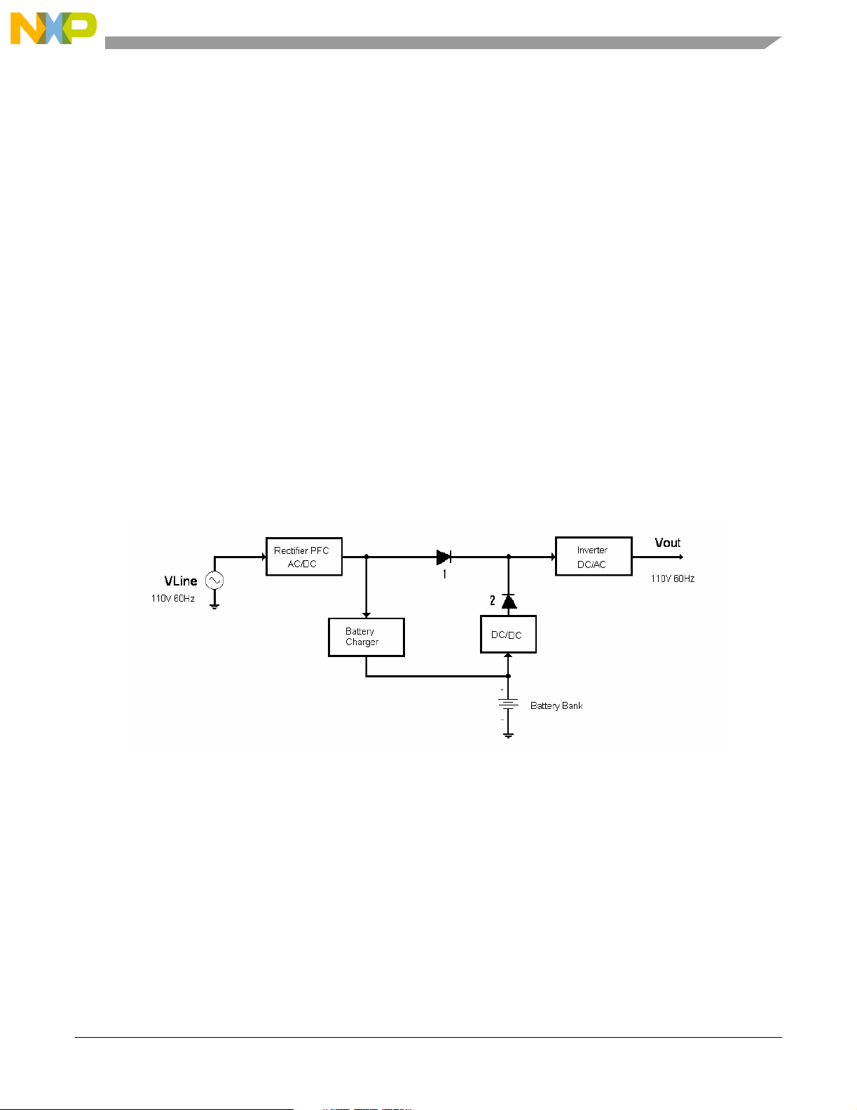
1.1.1 The Concept of an Online UPS
The minimum components needed to design an Online UPS are the rectifier, the battery bank and
the inverter. The rectifier converts the distribution line’s AC (Alternating Current) power to DC
(Direct Current), the form of current suitable to store energy in a battery bank. At all times, this
DC is also fed to an inverter, which reconverts the DC power to an AC waveform connected to
any equipment utilizing AC that a user considers as mission critical. If the AC supply fails for
any reason, the inverter will continue to draw power from the batteries.
Figure 1-1. A Basic Online UPS
1.1.2 Input Power Factor Control (PFC)
When a sinusoidal input signal is connected to a full wave rectifier, conduction will occur only
during the peaks of the signal. This causes a two-fold inconvenience to the electricity distribution
line:
• Insertion of harmonics to the lines
• High current peaks, which imply greater losses on the distribution
Online UPS Theory and Description, Rev. 0
Freescale Semiconduc tor 1-1
Preliminary
Page 18

These effects are aggravated by the long distances the electric distribution networks usually span.
From the electrical utility’s point of view, the best possible load is the pure resistive: The current
waveform should be a pure sinusoidal waveform identical to the voltage waveform and of the
same frequency and phase.
In order to show a resistive load to the utility lines, the input current to the UPS is controlled (i.e.,
modulated), to make it match a set point. This set point depends on the input voltage waveform,
and its amplitude is dependent on the equipment’s power consumption.
1.1.3 DC-to-DC Converters
If a rectifier is connected to the AC line supply, then the DC voltage will be equal to the peak
voltage of the line. (i.e., in a 120 V
configured for 12 or 24 V
, the UPS works by using DC-to-DC converters.
DC
line, the peak will be 120√2, 170V). If the battery bank is
RMS
For an online UPS, two power DC-to-DC converters are required. One converter operates as the
battery charger, and the other boosts the battery voltage in the absence of line input and generates
the appropriate DC required by the inverter.
1.1.4 Phase Locked Loop (PLL)
This UPS can operate in the Free Running mode or in the Locked-to-Line mode. If the AC main
line frequency is at the nominal value of 50Hz or 60Hz ± 5%, then the PLL locks the inverter
output to the line. If the AC main line frequency runs out of limits for any reason, the UPS will
automatically switch to run locked to the internal frequency reference.
The UPS will also work in the Free Running mode if commanded to operate as a frequency
converter. For example, it can connect to a 60Hz AC main line frequency and output a signal of
50Hz frequency, and vice versa.
The purpose of Phase-Locking the inverter to the line input is to enable the automatic bypass
feature, and to avoid signal “mixing” at the rails. These two features are detailed in the following
sections.
1.1.5 Bypass Operation
In order to allow a UPS bypass without loss of power at the load, two conditions must be met:
• The inverter output must be locked to the frequency and phase of the AC main line
• The inverter output and the AC main line’s RMS voltages must be within 10% of one
another
Online UPS Designer Reference Manual, Rev. 0
1-2 Freescale Semicond uctor
Preliminary
Page 19

Introduction
When the bypass conditions are met, the bypass switch can transfer the load to the AC main line
in the event of a UPS failure or when commanded by the operator during routine maintenance. It
can also switch the load back to the inverter after any maintenance.
1.1.6 Rail Ripple
The energy to support the load is stored in the rail capacitors. These capacitors are current-fed by
the PFC circuitry in the Online mode or by the battery booster in the Battery Back-up mode.
In the Online mode, a ripple with the phase and twice the frequency of the AC main line will be
present at the rails, superimposed with a ripple with the phase and twice the frequency of the
inverter current. In this situation, if a frequency offset ∆f is present, lower-order components can
appear. Locked operation is preferred to minimize the effects of frequency mixing.
1.1.7 Pulse Width Modula tion (PWM)
High-power control requires switchable electronic devices, precluding their use in the active
region, where power dissipation in the device is very high. For this reason, control is made by
pulse width modulation, where the duty cycle of a signal is modified, then a linear filtering
device passes the desired signal value to the analog components.
PWM is then used to implement inverters, PFCs, and DC-to-DC converters.
1.1.8 A Controller Solution to Control a UPS
The control system for a UPS must accomplish the following functions:
• Control strategies for inverter, PFC, PLL, and DC-to-DC converters. Every control loop
starts at an Analog-to-Digital Converter (ADC) in order to sense the signals, and ends at a
Pulse Width Modulator as an actuator.
• Deciding when to activate or deactivate a component
• Detecting failure conditions and implementing any required action
• Enabling Monitor and Control (M & C) communications
Compared to traditional analog controls, today’s low-cost and high-performance controllers
provide a better solution in performance and cost. A single MCU includes a powerful processor
core and such peripherals as PWMs, Timers, and Analog-to-Digital Converters. A single 56800E
device is able to assume the monitoring and real-time control required by an Online UPS.
Online UPS Theory and Description, Rev. 0
Freescale Semiconduc tor 1-3
Preliminary
Page 20
1.2 System Overview
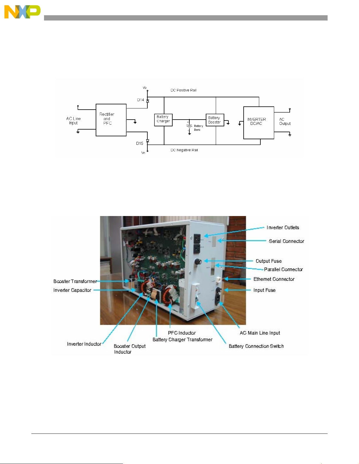
Figure 1-2 depicts a simplified UPS system.
Figure 1-2. UPS Simplified Schematic
Figure 1-3 shows a photo of a completed UPS prototype. The system’s power electronics and
ferromagnetic components are detailed on the left side of the the figure.
Figure 1-3. Prototype UPS
Online UPS Designer Reference Manual, Rev. 0
1-4 Freescale Semicond uctor
Preliminary
Page 21

System Actuators
1.3 System Actuators
A simplified schematic of the controller’s relationship with actuators is shown in Figure 1-4,
where all switches represent MOSFETs or IGBTs.
56800E Controller
Figure 1-4. Relationship between a 56800E and Power Actuators
Online UPS Theory and Description, Rev. 0
Freescale Semiconduc tor 1-5
Preliminary
Page 22
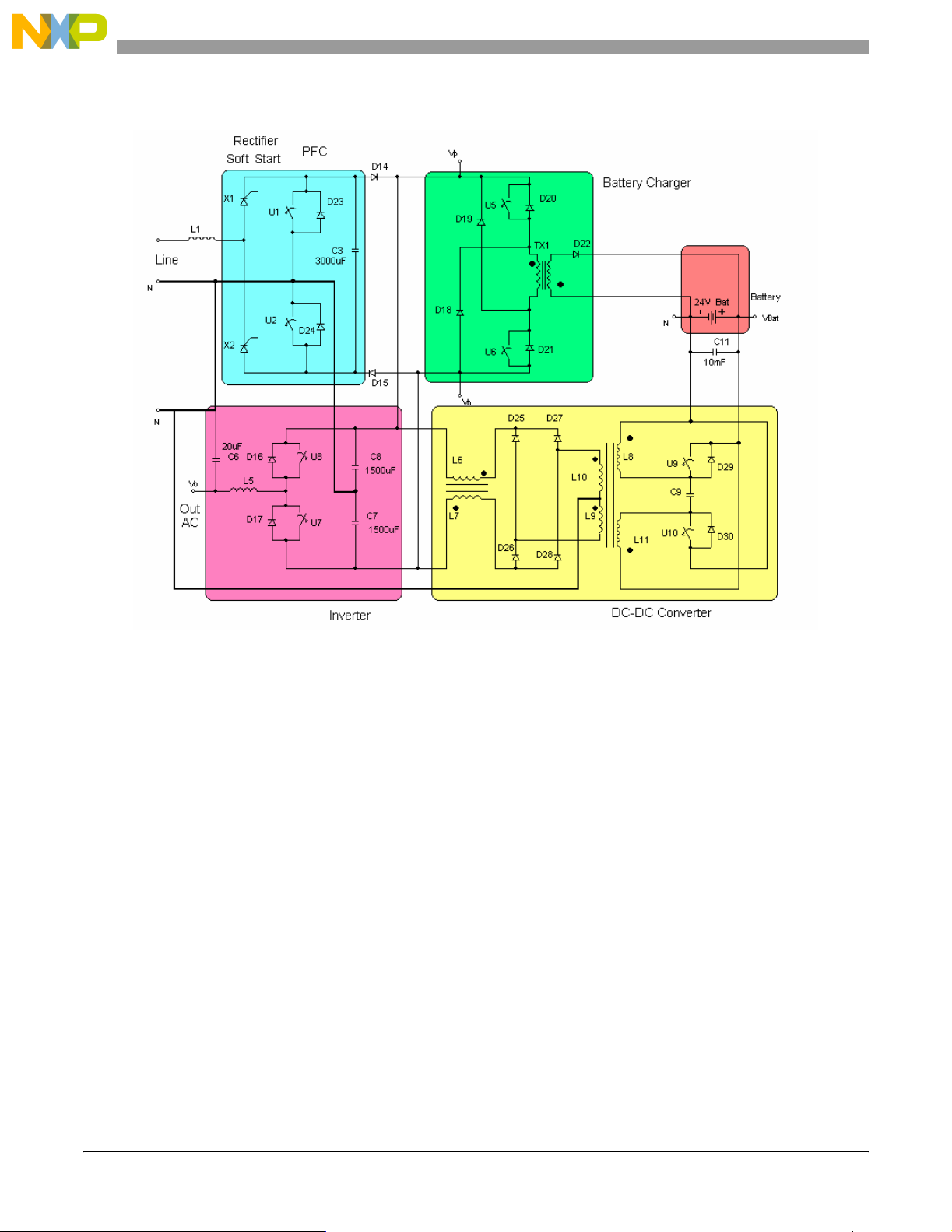
Figure 1-5. Simplified Schematic Diagram of the UPS
1.4 Input Rectifier Theory of Operation
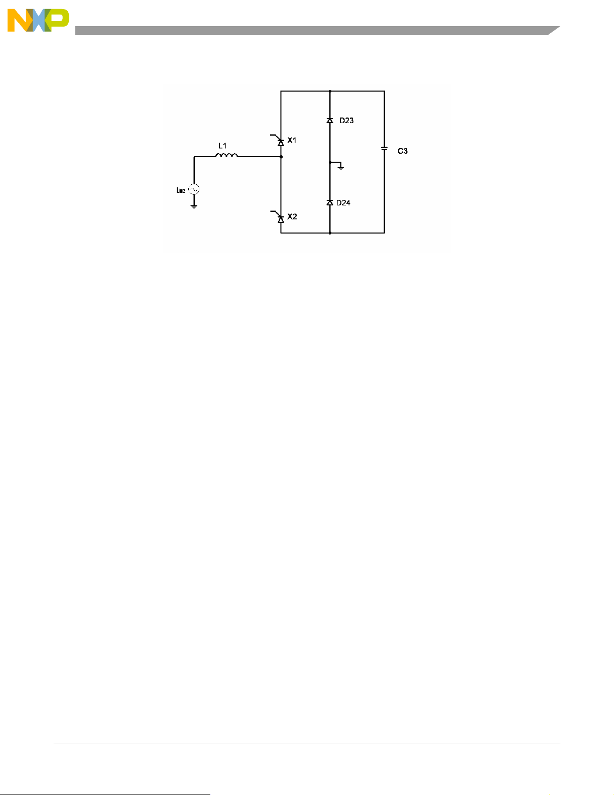
The input rectifier is implemented as a four-diode bridge (X1, X2, D24, and D23). A soft start
system implemented with SCRs can prevent a huge in-rush current when the system starts, while
the system’s internal capacitors get charged to the line’s peak voltage.
Online UPS Designer Reference Manual, Rev. 0
1-6 Freescale Semicond uctor
Preliminary
Page 23
Input Rectifier Theory of Operation
Figure 1-6. Input Rectifier
1.4.1 Rectifier Soft Start
If a high voltage is applied to a discharged capacitor, its low impedance will result in a very high
inrush current across the circuit, reducing the components’ longevity.
A soft start circuit is designed to avoid that circumstance. Figure 1-7 shows a full
wave-controlled rectifier bridge. If the trigger angle of X1 and X2 is gradually decreased from
the zero crossing towards the peak voltage, as demonstrated in Figure 1-8, the capacitor voltage
will then increase slowly. As the current on a capacitor equals the capacitance value times the
voltage derivative with respect to time, the input current will be proportional to the slope of the
voltage applied to the capacitor.
Online UPS Theory and Description, Rev. 0
Freescale Semiconduc tor 1-7
Preliminary
Page 24
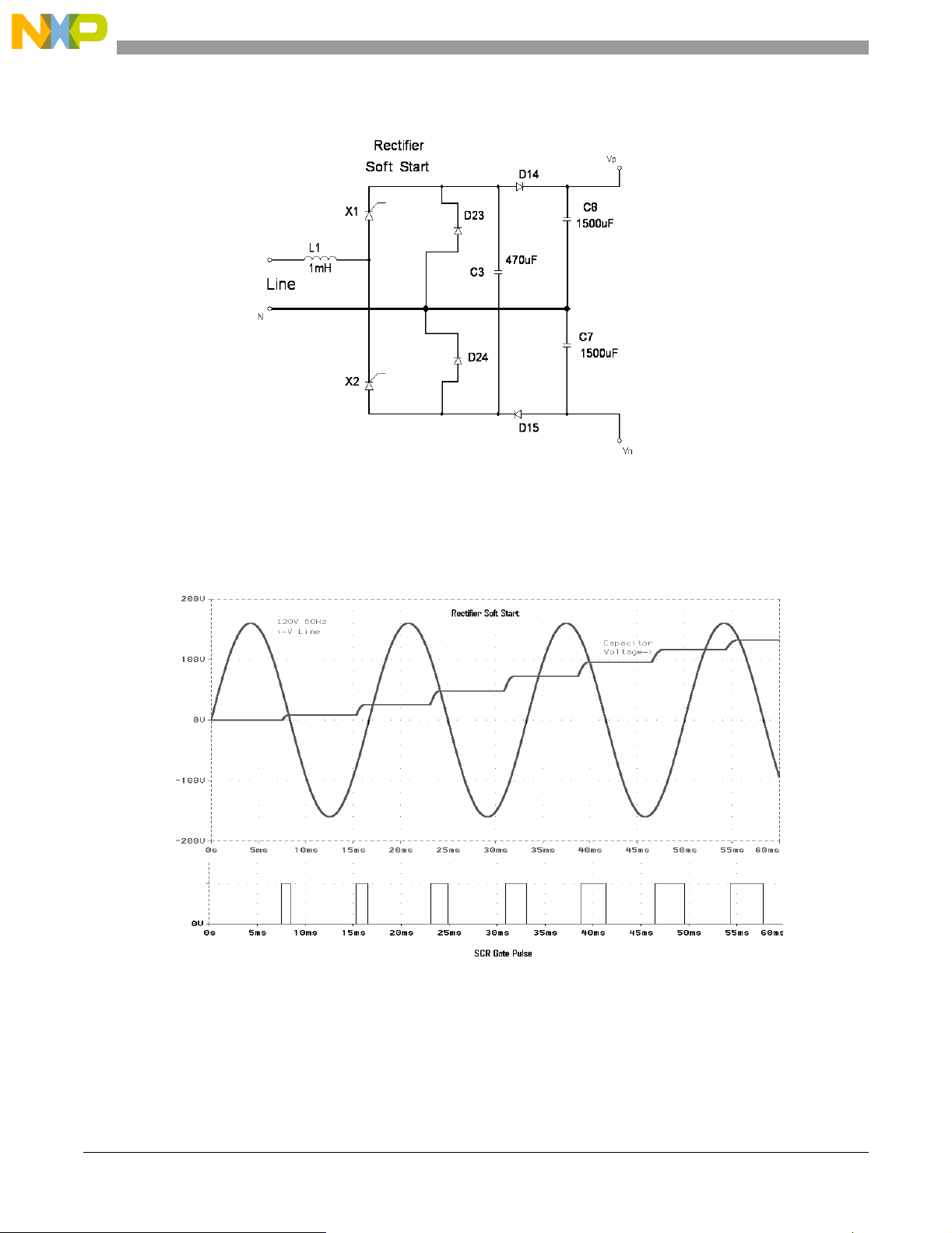
Figure 1-7. Full Wave-Controlled Rectifier Bridge
Figure 1-8. Relationship between Rectifier Soft Start Operation / Actuator Signals
and the AC Main Line Voltage
Online UPS Designer Reference Manual, Rev. 0
1-8 Freescale Semicond uctor
Preliminary
Page 25
Power Factor Corrector (PFC) Theory of Operation
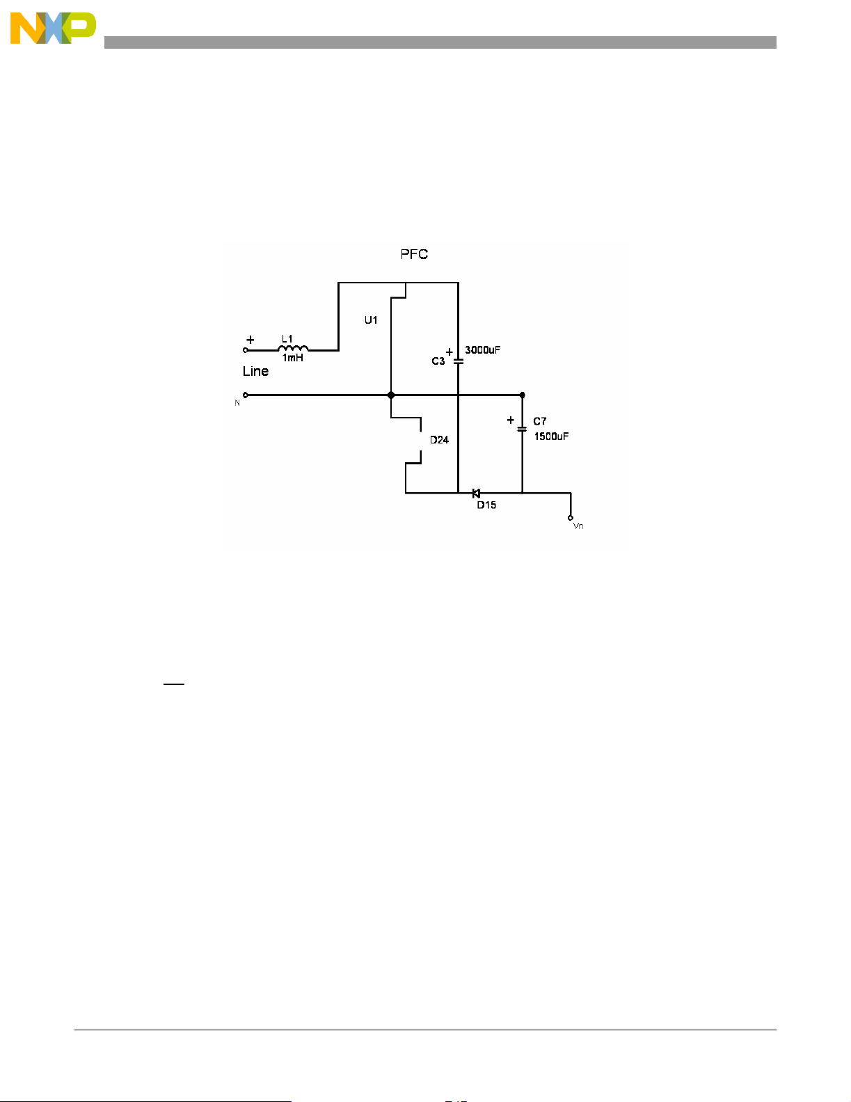
1.5 Power Factor Corrector (PFC) Theory of Operation
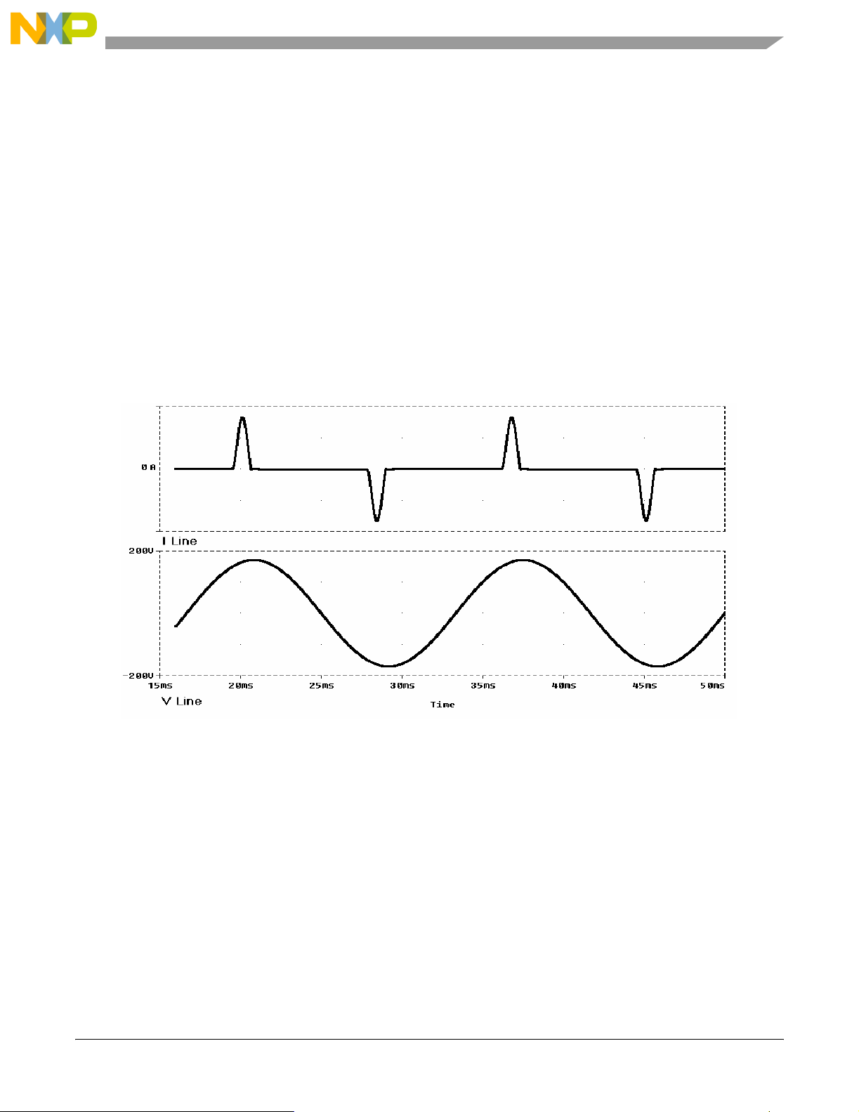
After the rectifier soft start finishes, X1 and X2 must act as diodes with continuous trigger. When
no PFC is implemented, the line current will be similar to that shown in Figure 1-9, due to the
diode–capacitor nature of a rectifier.
The objective of the PFC circuit is to simulate a resistive load to the power line; in other words, to
obtain a unity power factor and low harmonic content in the current waveform. A fast control
must be implemented in order to make the current waveform follow the AC voltage, while
elevating and controlling the rail voltage and supplying the average power required to the load.
Figure 1-10 shows how the PFC works, illustrating a current signal waveform similar in form to
the voltage waveform. The ripple in the figure is a consequence of the IGBT high frequency
switching.
Figure 1-9. Typical Rectifier Current vs. AC Line Voltage
Online UPS Theory and Description, Rev. 0
Freescale Semiconduc tor 1-9
Preliminary
Page 26
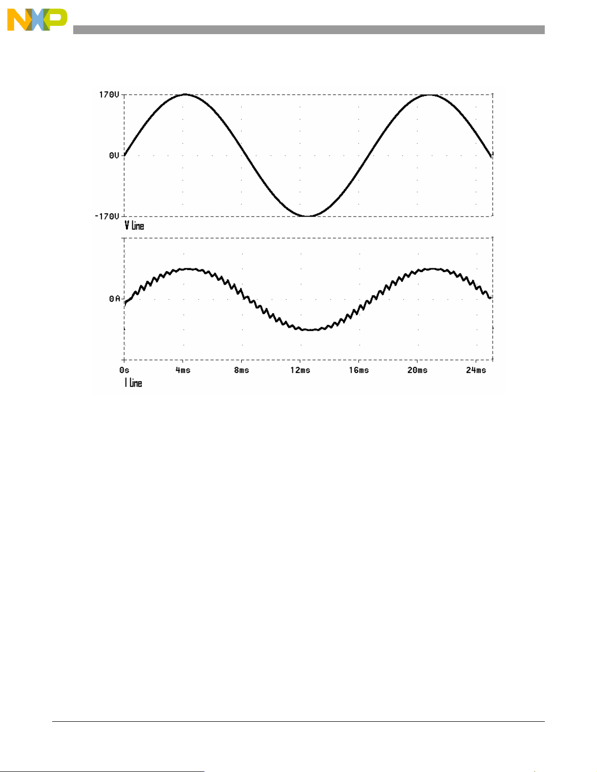
Figure 1-10. PFC Current and Voltage Waveforms
Once the voltage on capacitors C3, C7 and C
shown in Figure 1-11 reach the AC main supply
8
peak after the rectifier soft start, the PFC is turned on, correcting the power factor presented to
the line and generating the rail DC voltages V
Online UPS Designer Reference Manual, Rev. 0
and VN at a value higher than the line peak.
P
1-10 Freescale Semicond uctor
Preliminary
Page 27
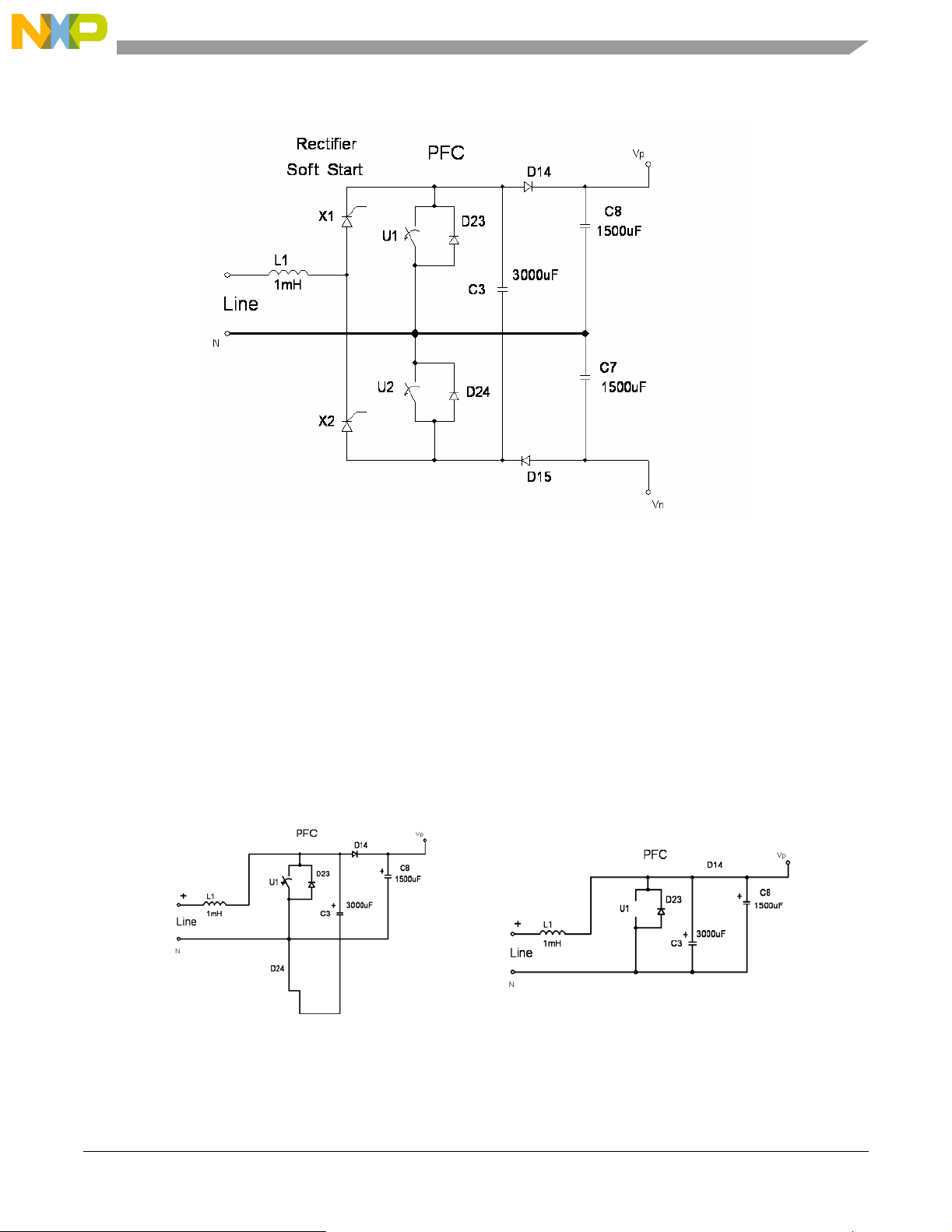
Power Factor Corrector (PFC) Theory of Operation
Figure 1-11. PFC Schematic
In order to work as a PFC, U1 and U
When U
is on, U2 is off, and vice versa.
1
in Figure 1-11 turn on and off in complementary mode.
2
The switching frequency of operation is 20kHz . The line nominal frequencies are 50Hz or 60Hz,
so it is a valid approximation to consider the line voltage as a constant during a switching period.
For positive values of the line, when U
that shown in Figure 1-12, where C
capacitors to be the same, thus reducing the ripple voltage on C
is on (closed) and U1 is off (open), the circuit reduces to
2
is connected in parallel to C8, causing the voltages on these
3
.
8
Figure 1-12. Partial PFC Schematic when U1 Is Open and U2 Is Closed
Online UPS Theory and Description, Rev. 0
Freescale Semiconduc tor 1-11
Preliminary
Page 28
For positive values of the line, when U1 is closed, and U2 is open, the circuit reduces as shown in
Figure 1-13, where C
line is applied directly to L
voltage could be considered constant, and the inductor current, which corresponds to the current
in the line (I
), depends on the voltage across its terminals.
LINE
is now connected in parallel to C7, thus reducing its ripple voltage. The
3
, increasing the current across it with a constant slope, because line
1
Figure 1-13. Partial PFC Schematic when U1 Is Closed and U2 Is Open
Inductor current is calculated by the equation:
t
1
I
=∆
L
Where:
V
is the voltage across the inductor terminals
L1
The peak current across the inductor at time t2 depends, among other factors, on the instant value
of the line voltage and the time difference t
2
∫
t
1
dtV
Lline
1
, which is the time that U1 remains closed.
2 – t1
Online UPS Designer Reference Manual, Rev. 0
1-12 Freescale Semicond uctor
Preliminary
Page 29
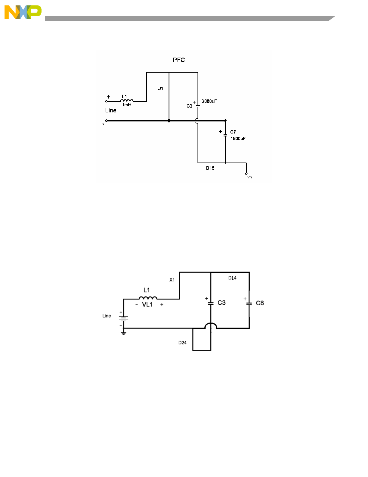
Power Factor Corrector (PFC) Theory of Operation
Figure 1-14. Resulting Parallel Connection between C3 and C7
The voltage-boosting characteristic of the PFC is accomplished by increasing the voltage across
(and consequently, across C7 and C8). Given that a current is circulating in the inductor L1,
C
3
when U
forces D
opens, the voltage across L
1
into a conduction state and C3 and C8 to charge to the addition of the line and the
24
inductor terminal voltage, V
Figure 1-15. Voltage Boost across Capacitors C3 and C
. This is a typical boost configuration.
L1
adds to the line voltage as shown in Figure 1-15. This
1
8
Due to symmetry, this circuit works in the same way for negative values in line voltage.
Online UPS Theory and Description, Rev. 0
Freescale Semiconduc tor 1-13
Preliminary
Page 30
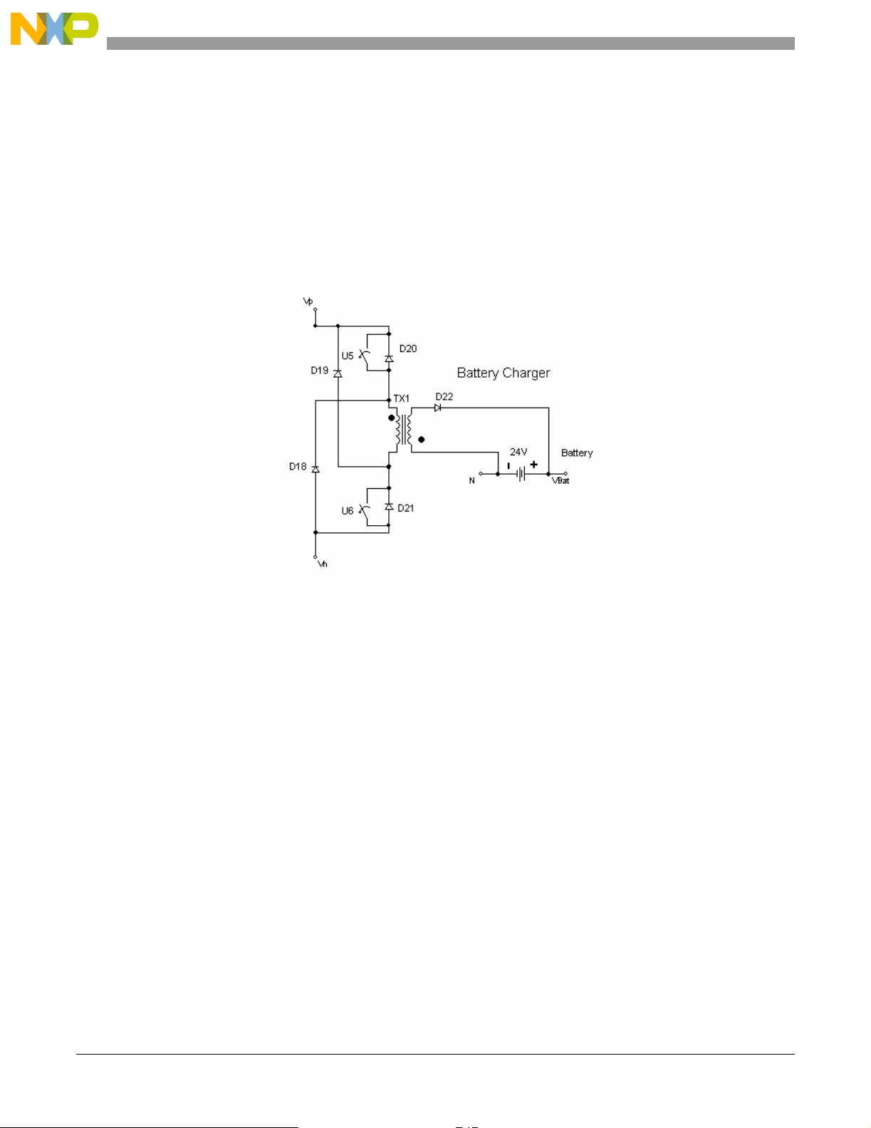
1.6 Battery Charger Theory of Operation
Figure 1-16 has been extracted from the UPS schematic shown in Figure 1-5. Using the high DC
voltages V
charge conditions for a battery bank formed by two 12V batteries connected in series, which must
be charged with constant current. When the float condition is reached, the charger must preserve
a constant voltage while providing the battery bank’s self-discharge current.
rail positive and VN rail negative as its power sources, this circuit provides the
P
Figure 1-16. Battery Charger Schematic
The battery charger is an application of a two-transistor flyback configuration using a coupling
inductor rather than a transformer. Because this operating mode implies no flow of current in the
secondary when the primary has a non-zero current, and vice versa, it means that no current flows
simultaneously in both windings.
Figure 1-16 shows a two-transistor version of a flyback converter, where U
and U6 are turned
5
on and off simultaneously. The advantage of such a topology over a single-transistor flyback
converter is that the switches’ voltage rating is V
through the diodes D
and D19, which are connected to the primary winding, a dissipative
18
- VN. Moreover, since a current path exists
P
snubber across the primary winding is not needed to dissipate the energy associated with the
transformer primary-winding leakage inductance.
The design, calculations and construction of TX
voltage from secondary to primary rising higher than V
are critical in order to prevent the reflected
1
- VN when D22 is on.
P
Online UPS Designer Reference Manual, Rev. 0
1-14 Freescale Semicond uctor
Preliminary
Page 31

Battery Booster Theory of Operation
1.7 Battery Booster Theory of Operation
The battery booster is a DC-to-DC converter and transforms the battery voltage of 24VDC to the
required differential 440V
the positive rail, and V
N
Although the topology of Figure 1-17 is usually called “booster” because its output voltage is
higher than input voltage, it is actually a push-pull converter with an arrangement of two forward
converters working alternatively and a transformer to increase the output voltage.
between rails. The rails are symmetric, implying VP = 220VDC at
DC
= -220V
at the negative rail, as shown in Figure 1-17.
DC
Figure 1-17. Battery Booster Schematic
The switches U9 and U10 cannot be closed at the same time. Typical drive signals are illustrated
in Figure 1-18.
Online UPS Theory and Description, Rev. 0
Freescale Semiconduc tor 1-15
Preliminary
Page 32

Figure 1-18. Drive Signals for Battery Booster Switches
Using a control signal like the one shown in Figure 1-18, the waveforms at the transformer
secondary over L
and L9 are illustrated with positive and negative values of voltage in
10
Figure 1-19.
Figure 1-19. Signals at Transformer Secondary Windings L10 and L
C9 remains charged to V
and is added because the coupling factor is not equal to one,
BAT
implying that a leakage inductor must be considered. C
acts as a snubber, creating a current path
9
9
to avoid an uncontrolled voltage peak at the primary windings of the transformer.
Online UPS Designer Reference Manual, Rev. 0
1-16 Freescale Semicond uctor
Preliminary
Page 33

Battery Booster Theory of Operation
The four diodes D25, D26, D27 and D28 form a conventional full-wave rectifier bridge and
generate only positive values in the cathodes of D25 and D27 and negative values at the anodes
of D26 and D28, as shown in Figure 1-20.
Figure 1-20. Signals at the Cathode of D25 and Anode of D
26
The objective of DC/DC converters is to generate a DC voltage. In order to filter any undesirable
AC components, two LC filters are added:
•L
•L
for the negative rail
7-C7
for the positive rail
6-C8
Online UPS Theory and Description, Rev. 0
Freescale Semiconduc tor 1-17
Preliminary
Page 34

1.8 Inverter Theory of Operation
⎞
⎛
Figure 1-21. Inverter Schematic Diagram
The chosen inverter configuration is a half-bridge monophasic circuit. It must generate a
low-distortion sinusoidal waveform in the output terminals from the V
To produce such a signal, V
and VN must be higher than the AC positive and negative peak
P
voltages, respectively.
and VN DC rail voltages.
P
Consider a switching period of T seconds. Assume that U
is open. During the remaining T – T
of the low-pass filter composed by inductor L
seconds, U7 is closed and U8 open. If the cutoff frequency
P
and C6 is low enough to reject the 1/T Hz
5
switching frequency, then the output approximates to:
t
p
VV
Po
T
t
p
T
1
,1
=<
T
Where:
tp/T is the duty cycle of the control signal
t
p
⎜
N
⎜
⎝
⎟
1V
−+=
⎟
T
⎠
kHz20
is closed during TP seconds, while U7
8
Online UPS Designer Reference Manual, Rev. 0
1-18 Freescale Semicond uctor
Preliminary
Page 35

Auxiliary Circuits
The expression simplifies to :
t
()
p
VVV
NPo
V
+−=
T
N
As 1/T = 20kHz is much higher than 50Hz or 60Hz, then the output voltage will result
proportional to T
, and the sinusoidal signal can be considered constant during T seconds.
P
1.9 Pulse Width Modulation
If a sinusoidal reference signal is compared to a symmetric triangle wave, the resulting signal is
pulse width modulated, as shown in Figure 1-22. The triangle waveform frequency corresponds
to the PWM switching frequency.
Figure 1-22. Generation of a PWM Signal
1.10 Auxiliary Circuits
Additional circuits are required to make the complete system operational and include.
• Power supplies
• Signal sensing circuitry
Online UPS Theory and Description, Rev. 0
Freescale Semiconduc tor 1-19
Preliminary
Page 36

• Limiters
• Isolation circuits
• Driver circuits for SCRs, NMOSFETs and IGBTs
1.10.1 Power Supplies and Isolation Circuitry
This system requires multiple power supplies with floating references. The typical configuration
is shown in Figure 1-23, and consists of a flyback converter similar to the one used in the battery
charger. A 100kHz switching signal with a duty cycle of 35% is provided by the 56800E
controller and applied to an NMOS technology H bridge.
Figure 1-23. H Bridge Configuration used to Provide Multiple Floating Power Supplies
The output of the isolating transformer is half-wave rectified and applied to the load. Positive and
negative voltages are generated. The 39Ω resistor limits the current of the transformer’s
secondary when M
and M2 are on. Resistors RL1 and RL2 represent the load.
1
All isolated power supplies are connected in parallel to the rail voltage, depicted as nodes A and
B in Figure 1-23.
Online UPS Designer Reference Manual, Rev. 0
1-20 Freescale Semicond uctor
Preliminary
Page 37

Figure 1-24. Waveforms at A and B
Auxiliary Circuits
While M1 and M2 are on, VCC is connected directly to the primary, increasing the current
linearly, as shown in Figure 1-25. C
acts as a current limiter. M
, M2, Dp, Cp, and the transformer shape a traditional flyback power
1
is simultaneously charging across Dn. The 39Ω resistor
n
supply.
Online UPS Theory and Description, Rev. 0
Freescale Semiconduc tor 1-21
Preliminary
Page 38

Figure 1-25. Current Waveforms
When M1 and M2 are off, an inverted voltage is induced in the primary and D1, D2 which limit
that voltage to 15V plus 1.2 from two diode junctures, turning D
on and charging Cp.
p
There are several transformers connected to the rails A and B which generate isolated power
supplies to drive SCRs, IGBTs, and MOSFETs used in the rectifier, inverter, battery charger, and
battery booster.
Figure 1-26 shows the control power supply, which uses a LM2576 step-down voltage regulator,
to generate +V
additional power supply V
= 15V fed by the redundant DC voltage coming from 18VAC or +V
CC
coming from the battery charger. This circuit also generates the
DCR
Control Board Power Supply, which is isolated from +V
CC
.
BAT
or an
Online UPS Designer Reference Manual, Rev. 0
1-22 Freescale Semicond uctor
Preliminary
Page 39

Figure 1-26. Control Power Supply
1.10.2 Sensing Circuits and Reference Voltage Generator
Auxiliary Circuits
All signals that require sensing as voltages, currents, and temperature at the Analog-to-Digital
Converters are converted to the appropriate input levels and diode-limited to avoid damage to the
ADCs; this process uses differential amplifiers as seen in Figure 1-28, because of the different
ground references shown in Figure 1-27.
Online UPS Theory and Description, Rev. 0
Freescale Semiconduc tor 1-23
Preliminary
Page 40

Controller
Figure 1-27. Partial View of the Auxiliary Power Supply and Optoisolation Network
Figure 1-28. General Design of the Sensing Circuits
Online UPS Designer Reference Manual, Rev. 0
1-24 Freescale Semicond uctor
Preliminary
Page 41

Auxiliary Circuits
The value of the resistors required to sense every signal are calculated in order to guarantee full
swing, minimizing analog and quantization noise at the ADCs.
The reference level of the ADC is used to shift the AC input signal to swing from 0 to V
0 volts in the input signal are mapped to V
/2). If the output of the operational amplifier tends
RH
RH
to go out of limits for any reason, the diodes protect the ADC inputs.
1.10.3 Voltage Reference Supply
The voltage reference, V
a buffer to the reference voltage V
auxiliary voltage outputs:
•V
•V
equal to one diode voltage Vγ
A
with value VRH-Vγ
B
These voltages will be used to limit the values of voltage applied to A/D modules inside the
controller.
, is generated by the circuit shown in Figure 1-29. This circuit acts as
RH
from the controller. This circuit also generates two
REFH
(i.e.,
Figure 1-29. Voltage Reference Generator
Online UPS Theory and Description, Rev. 0
Freescale Semiconduc tor 1-25
Preliminary
Page 42

1.10.4 Silicon Controlled Rectifier (SCR) Gate Drivers
The circuit in Figure 1-30 shows the basic driver which handles the SCRs’ gates using an 4N35
optocoupler to generate an isolated current supply to trigger the rectifier’s SCRs.
Figure 1-30. SCR Gate Driver
1.10.5 IGBT and MOSFET Gate Drivers Circuit
Figure 1-31 illustrates the basic isolated circuit implemented to drive the IGBT’s and
MOSFET’s gates. It is based in a HCPL 3101 gate drive optocoupler.
Figure 1-31. IGBT and MOSFET Gate Driver
Online UPS Designer Reference Manual, Rev. 0
1-26 Freescale Semicond uctor
Preliminary
Page 43

Power Transfer Circuits (Bypass) Theory of Operation
1.11 Power Transfer Circuits (Bypass) Theory of Operation
Under normal conditions, the UPS inverter feeds all power to the load. However, in order to
ensure that the load is supported in the event of a failure, or during maintenance, the equipment
must also allow for direct connection to the AC main line. A switching relay is connected as
shown in Figure 1-32.
Figure 1-32. Bypass Relay Configuration
The relay’s transfer time must be shorter than a period of the AC line. A transfer time of less than
20ms is fast enough to comply with this constraint. The transfer is allowed if phase and voltage
conditions are satisfied, as explained in
Figure 1-33 shows the circuit implemented to turn the bypass relay on and off using the BP
Section 1.1.4.
1
signal. Please note the three different grounds used in the system.
Online UPS Theory and Description, Rev. 0
Freescale Semiconduc tor 1-27
Preliminary
Page 44

Figure 1-33. Relay Driver
1.12 Overcurrent Protection
Figure 1-34 shows the rectifier and inverter current sensing circuit. Figure 1-35 shows the
circuits implemented to sense the battery charger and battery booster currents. These circuits
generate overcurrent signals when the current value reaches a defined level. These two signals
are connected directly to the controller’s FAULT 0 and FAULT 1 pins.
Online UPS Designer Reference Manual, Rev. 0
1-28 Freescale Semicond uctor
Preliminary
Page 45

Overcurrent Protection
Figure 1-34. Overcurrent Protection for Rectifier and Inverter
Figure 1-35. Overcurrent Protection for Charger and Push-Pull
Online UPS Theory and Description, Rev. 0
Freescale Semiconduc tor 1-29
Preliminary
Page 46

The battery charger overcurrent protection generates a fault signal, named “SIC”, which turns off
the charger PWM signal. Likewise, the battery booster’s overcurrent protection circuit generates
the FPP signal, which turns off the drive signal for the MOSFETS.
1.13 Battery Temperature Sensing
The battery temperature sensing circuit is shown in Figure 1-36; it uses an LM-35-CZ, which is a
precision centigrade temperature sensor. The output of this circuit is a voltage that is proportional
to the temperature. This sensor must be located near the battery.
Figure 1-36. Battery Temperature Sensing Circuitry
Online UPS Designer Reference Manual, Rev. 0
1-30 Freescale Semicond uctor
Preliminary
Page 47

Battery Temperature Sensing
Figure 1-37. Battery Temperature Sensor
Online UPS Theory and Description, Rev. 0
Freescale Semiconduc tor 1-31
Preliminary
Page 48

Online UPS Designer Reference Manual, Rev. 0
1-32 Freescale Semicond uctor
Preliminary
Page 49

Control Algorithms Discrete Equivalents
⎞
⎛
Chapter 2 Control Loops In The Online
UPS
The UPS’s control algorithms are digitally implemented. The topology chosen for the
compensators is the PID (Proportional – Integral – Derivative) and the PI (Proportional –
Integral), with a 3- bit resolution. All gain constants are 16-bit implemented. The accumulators
are all 32-bit, unless otherwise specified.
2.1 Control Algorithms Discrete Equivalents
An ideal PID analog controller is expressed as follows:
1
⎜
KsGc
1)(
+=
p
⎜
⎝
s
τ
⋅
i
⎟
s
⋅+
τ
d
⎟
⎠
An appropriate technique to discretize this transfer function is the backward difference method,
which is based on numerical integration theory and has the following equivalence rule:
1
−
d
s
→→
dt
z
)1(
−
T
s
Where:
is the sampling period
T
s
The PID transfer function in discrete time domain is:
1
−
TK
⋅
K)z(G
+=
pc
i
sp
+
1
−
)z1(
−⋅τ
dp
T
s
)z1(K
−⋅τ⋅
It is implemented as follows:
k
∑
IP
j
0
=
Freescale Semiconduc tor 2-1
Preliminary
[]
D
Control Loops In The Online UPS, Rev. 0
)1()()()()(
kekeKjeKkeKkC
−−⋅+⋅+⋅=
Page 50

Where:
TK
⋅
K
=
I
sp
τ
i
is the discrete time integrator gain
and
K
τ
⋅
K
=
D
dp
T
s
is the discrete time differential gain
The proportional gain constant, K
, remains unmodified.
P
2.2 PFC and Rail Control
Figure 2-1 shows a simplified PFC control loop, valid only for positive AC line voltages. The
PFC is a current loop with a set point calculated as the product of the rail voltage control output
times the AC line voltage.
The voltage control must keep a constant DC rail. V. Positive Rail is sensed and compared to
Voltage Setpoint. The error signal then passes through a PI control network, which outputs one of
the operands used to calculate the current set point. The other operand is the AC Line Voltage,
V
control loop.
. This signal is then used as the set point of a second PI control, which forms the current
LINE
Online UPS Designer Reference Manual, Rev. 0
2-2 Freescale Semicond uctor
Preliminary
Page 51

PFC and Rail Control
⎞
⎛
Figure 2-1. PFC and Rail Control Loops (Positive Semicycle)
The goal of the rectifier stage is to maintain the rail DC voltage at ± 220V and to control the input
current to mimic the voltage waveform (and thus to make the complete system appear as a
resistive load to the AC main line). In order to achieve these two goals, two control loops are
required:
A current control loop, implemented with a PI controller, which generates a current as required
by the input inductor. Due to the circuit symmetry, it is possible to implement a control using the
line voltage absolute value to control the signal, regardless of its sign. A suitable controller for
this application is a PI compensator with the following parameters:
14.6)s(Gc
⎜
⎝
1
+=
⎟
s0002.0
⋅
⎠
Control Loops In The Online UPS, Rev. 0
Freescale Semiconduc tor 2-3
Preliminary
Page 52

Using the backward difference method yields the following discrete time equivalent:
⎞
⎛
k
jeKkeKkC
)()()(
∑
⋅+⋅=
IP
j
0
=
With :
K
= 6.4
P
and
= 1.6
K
I
The second controller keeps the rail voltage constant and uses a low pass filter to reject the 60Hz
and 120Hz ripple. The process is much slower than any of these frequencies, and therefore should
not attempt to correct higher harmonic disturbances. The chosen controller is a PI. The output of
this controller modulates the AC main line voltage to obtain the reference for the current loop.
The low-pass filter is a first-order Infinite Impulse Response (IIR) filter with a 3dB cutoff
frequency of 5Hz, implemented with the following transfer function:
zf
)(
)(
ze
zb
⋅
0
=
az
−
1
With:
= 0.01
b
0
= 0.9984
a
1
The following is the proper PI controller:
sGc
19.0)(
⎜
⎝
1
+=
0563.0
⎟
s
⋅
⎠
Using the backward difference method yields the following discrete time equivalent:
k
jeKkeKkC
)()()(
∑
⋅+⋅=
IP
j
0
=
With:
= 0.9
K
P
and
K
= 0.0008
I
Online UPS Designer Reference Manual, Rev. 0
2-4 Freescale Semicond uctor
Preliminary
Page 53

Battery Charger Control
2.3 Battery Charger Control
The circuit in Figure 2-2 shows a schematic battery charger control loop, consisting of an inner
voltage loop and an outer current loop. The sensed battery voltage determines the charging
current (limited to 1 Ampere). This current is a function of the PWM duty cycle.
Figure 2-2. Battery Charger Control Loop
Given that the battery voltage is a slow signal, the sampling frequency for this control is
decimated by 16 relative to the 20kHz (20kHz/16 = 1250Hz) sampling frequency used elsewhere
in the system. The PWM switching frequency is preserved at 20kHz.
In order to avoid saturation of the voltage compensating network’s integrator, its input is
deactivated if the control output is above a predefined threshold.
The batteries are charged using the constant current–constant voltage approach. While the battery
voltage is lower than the floating voltage (in this case 28V), a constant current of 1A is applied.
When the battery terminal voltage reaches 28V, the voltage is kept constant, decreasing the
charge current. The battery charger system is implemented by two nested loops. The inner loop
controls the charging current and uses a PI control. The reference for this control is delivered by a
voltage control loop, whose output is limited from 0 to 1/3, where 1/3 (in Frac16 notation)
represents 1A. When the batteries are discharged, the voltage control increases the current
Control Loops In The Online UPS, Rev. 0
Freescale Semiconduc tor 2-5
Preliminary
Page 54

reference, looking for a 28V voltage. However, when the voltage control loop reaches 1/3, the
⎞
⎛
⎞
⎛
integral action is disconnected and the output is limited, forcing the current loop to set a 1A
charging current to the battery. When floating voltage is reached, the voltage control loop reduces
its output, reducing the current applied to the batteries.
The controller chosen for the current control loop is a PI compensator with the following
parameters:
17.0)s(Gc
⎜
⎝
1
+=
⎟
s001.0
⋅
⎠
Using the backward difference method results in the following discrete time equivalent system:
k
jeKkeKkC
)()()(
∑
⋅+⋅=
IP
j
0
=
With:
= 0.7
K
P
and
K
= 0.035
I
The controller chosen for the voltage control loop is a PI compensator with the following
parameters:
sGc
12.0)(
⎜
⎝
1
+=
⎟
se
332
⋅−
⎠
Using the backward difference method results in the following discrete time equivalent system:
k
jeKkeKkC
)()()(
∑
⋅+⋅=
IP
j
0
=
with:
= 0.02
K
P
and
= 0.0005
K
I
Online UPS Designer Reference Manual, Rev. 0
2-6 Freescale Semicond uctor
Preliminary
Page 55

Inverter Control
⎟
⎠
⎞
⎛
2.4 Inverter Control
The objective of the inverter control loop is to supply the load with a voltage defined by the
reference signal. This reference signal is generated by the PLL system, at a sampling frequency
of 20kHz, high above the 50/60Hz nominal frequency. For this reason, it is reasonable to
consider the set point a constant.
Figure 2-3. Inverter Control Loop
The inverter control is implemented with a nested topology. The outer loop controls the output
voltage and the inner loop controls the inductor current. This configuration allows better stability
of the feedback system and an implicit limitation of the current delivered to the load. The inner
control loop stabilizes the system, acting as a damper for the LC output circuit.
The controller chosen for the current control loop is a PI compensator with the following
parameters:
sGc
Freescale Semiconduc tor 2-7
Preliminary
184.0)(
⎜
⎝
1
+=
0017.0
s
⋅
Control Loops In The Online UPS, Rev. 0
Page 56

Using the backward difference method results in the following discrete time equivalent system:
⎞
⎛
k
jeKkeKkC
)()()(
∑
⋅+⋅=
IP
j
0
=
With:
K
= 0.84
P
and
K
= 0.0024
I
The outer loop is the voltage control. The goal of this loop is to keep a sinusoidal voltage
waveform, regardless of the load characteristics. When nonlinear loads (as a full wave rectifier)
are connected, a high current is drawn at the peaks of the signal. The action taken to overcome
this condition is to inhibit the integral action by disconnecting the integrator input when the
current draw is high. This action reduces the output distortion and enhances the controller
response when the load requires high currents.
The controller chosen for the current control loop is a PI compensator with the following
parameters:
142.3)s(Gc
+=
⎜
⎝
1
s00036.0
⋅
s0001688.0
⋅+
⎟
⎠
Using the backward difference method results in the following discrete time equivalent system:
k
∑
j
IP
0
=
[]
D
)1()()()()(
kekeKjeKkeKkC
−−⋅+⋅+⋅=
With:
= 3.42
K
P
K
= 0.475
I
and
= 11.75
K
D
2.5 Battery Booster Control Loop
The function of this controller is to keep the rail DC voltage at ±220V while the system is
supported by the battery.
Online UPS Designer Reference Manual, Rev. 0
2-8 Freescale Semicond uctor
Preliminary
Page 57

Battery Booster Control Loop
⎞
⎛
Figure 2-4. Battery Booster Control Loop
Given that the rail voltage is a slow signal, the sampling frequency for this control is decimated
by 16 relative to the 20kHz (20kHz/16 = 1250Hz) sampling frequency used in other sections of
the system. The PWM switching frequency is preserved at 20kHz.
The system is implemented with a PID compensator in order to regulate the rail DC voltage. The
control output modulates the duty cycle of a push-pull power supply. The following are the
parameters of such a controller:
116)s(Gc
⎜
⎝
1
+=
s064.0
⋅
s000005.0
⋅+
⎟
⎠
Using the backward difference method yields the following discrete time equivalent system:
k
∑
j
[]
IP
0
=
D
)1()()()()(
kekeKjeKkeKkC
−−⋅+⋅+⋅=
With:
= 16
K
P
K
= 0.2
I
and
= 0.1
K
D
Control Loops In The Online UPS, Rev. 0
Freescale Semiconduc tor 2-9
Preliminary
Page 58

2.6 Minimizing Delay in the Control Loops
⎞
⎛
The triangular signal used as a carrier wave for the PWM is created from a counter that
accumulates at the controller’s clock speed (60MHz). The pulse width of the PWM is updated at
a rate of 20kHz. This implies that in order to obtain both the 20kHz sampling frequency and a
symmetric triangle wave, this counter must count from zero to 1500, then count back from 1500
to zero:
MHz
60
1
⎜
KHz
20
2
⎝
Given that the PWM(s) update their value when the PWM load command is given to the PWM
peripheral, the delay from the time elapsed between the sampling of the signal and the update of
the PWM compare values should be minimized, enhancing the system’s stability. The
implementation of this delay and the relationship between the PWM reference and the ADC
conversion is fully explained in
1500
=
⎟
⎠
Section 5.
Online UPS Designer Reference Manual, Rev. 0
2-10 Freescale Semicond uctor
Preliminary
Page 59

Chapter 3 Control Board Design
Considerations
3.1 56F8346 Controller
56F8346 Controller
Two source voltages are needed: one for the V
is provided to connect/disconnect the Temperature Sense Diode to the ADCA, Channel 7 (ANA7).
pins and the other for the ADC module. Jumper JG8
DD_IO
Control Board Design Considerations, Rev. 0
Freescale Semiconduc tor 3-1
Preliminary
Page 60

C15
2.2uF
EMI_MODE
+
C12
2.2uF
Use on-chip
regulators
/CS0
/CS1
/CS2
/CS3
/WR
/IRQA
/IRQB
EXTBOOT
XTA L
EXTAL
CLKO
/RESET
MISO0
MOSI0
SCLK0
/SS0
TDO
TCK
/TRST
TMS
+
U1
ISA0/PC8
ISA1/PC9
ISA2/PC10
FAULTA0
FAULTA1
FAULTA2
PHA0/TA0
PHB0/TA1
INDEX0/TA2/PC6
HOME0/TA3/PC7
ISB0/PD10
ISB1/PD11
ISB2/PD12
FAULTB0
FAULTB1
FAULTB2
FAULTB3
INDEX1/TB2/MISO1/PC2
PHB1/TB1/MOSI1/PC1
PHA1/TB0/SCLK1/PC0
HOME1/TB3/SS1/PC3
TC0/PE8
TD0/PE10
TD1/PE11
CAN_RX
TEMP_SENSE
TXD0/PE0
RXD0/PE1
TXD1/PD6
RXD1/PD7
VDDA_OSC_PLL
VDDA_ADC
VSSA_ADC
VREFMID
VREFLO
MC56F8346
PWMA0
PWMA1
PWMA2
PWMA3
PWMA4
PWMA5
ANA0
ANA1
ANA2
ANA3
ANA4
ANA5
ANA6
ANA7
PWMB0
PWMB1
PWMB2
PWMB3
PWMB4
PWMB5
ANB0
ANB1
ANB2
ANB3
ANB4
ANB5
ANB6
ANB7
CAN_TX
VREFH
VREFP
VREFN
62
64
65
67
68
70
113
114
115
71
73
74
139
140
141
142
88
89
90
91
92
93
94
95
34
35
36
39
40
41
50
52
53
56
57
58
61
104
105
106
107
108
109
110
111
8
7
6
9
118
116
117
126
127
96
4
5
42
43
80
102
103
101
100
99
98
97
PC2
+3.3V_PLL
C47
0.1uF
+VREFH
C48
0.1uF
PWMA0
PWMA1
PWMA2
PWMA3
PWMA4
PWMA5
PC8
PC9
PC10
FAULTA0
FAULTA1
FAULTA2
PHASEA0
PHASEB0
PC6
PC7
ANA0
ANA1
ANA2
ANA3
ANA4
ANA5
ANA6
ANA7
PWMB0
PWMB1
PWMB2
PWMB3
PWMB4
PWMB5
PD10
PD11
PD12
FAULTB0
FAULTB1
FAULTB2
FAULTB3
ANB0
ANB1
ANB2
ANB3
ANB4
ANB5
ANB6
ANB7
PC1
PC0
PC3
PE8
RXTXEN
CESI
CAN_TX
CAN_RX
TXD0
RXD0
PD6
PD7
C82
0.001uF
C49
0.1uF
FAULTA0
FAULTA1
FAULTA2
FAULTB0
FAULTB1
FAULTB2
FAULTB3
JG8
1
ANA7
2
+3.3VA
C87
100pF
Single trace
to GNDA
C19
0.1uF
Single trace
to GNDA
JG1
R60
47K
R61
47K
R62
47K
R64
47K
R65
47K
R54
47K
R63
47K
+3.3V
R36
1K
CLKMODE
2
1
PB0
CLKMODE
/RSTO
+
138
133
134
135
136
137
112
143
131
132
130
129
123
124
121
120
122
119
125
128
144
10
11
12
13
14
17
18
19
20
21
22
23
24
25
26
33
59
60
72
75
76
77
78
28
29
30
32
46
47
48
49
44
45
54
55
81
82
3
87
86
85
1
16
31
38
66
84
2
51
83
15
27
37
63
69
79
A0
A1
A2
A3
A4
A5
A6/PE2
A7/PE3
A8/PA0
A9/PA1
A10/PA2
A11/PA3
A12/PA4
A13/PA5
A14/PA6
A15/PA7
PB0/A16
D0
D1
D2
D3
D4
D5
D6
D7/PF0
D8/PF1
D9/PF2
D10/PF3
D11/PF4
D12/PF5
D13/PF6
D14/PF7
D15
PS/CS0
DS/CS1
PD0/CS2
PD1/CS3
WR
RD
IRQA
IRQB
EXTBOOT
EMI_MODE
XTA L
EXTAL
CLKO
CLKMODE
RESET
RSTO
MIS O0/PE6
MOSI0/PE5
SCLK0/ PE4
SS0/PE7
TDI
TDO
TCK
TRST
TMS
VDD_IO1
VDD_IO2
VDD_IO3
VDD_IO4
VDD_IO5
VDD_IO6
VDD_IO7
VPP1
VPP2
VCAPC1
VCAPC2
VCAPC3
VCAPC4
VSS_IO1
VSS_IO2
VSS_IO3
VSS_IO4
VSS_IO5
REG_EN
A0
A1
A2
A3
A4
A5
A6
A7
A8
A9
A10
A11
A12
A13
A14
A15
D0
D1
D2
D3
D4
D5
D6
D7
D8
D9
D10
D11
D12
D13
D14
D15
/RD
TDI
+3.3V
+
C13
C14
2.2uF
2.2uF
Figure 3-1. 56F8346 Controller
The Control Board provides a Clock Boot Mode jumper, JG1. This jumper is used to select the
type of clock source being provided to the processor as it exits reset. The user can select between
the use of a crystal or an oscillator as the clock source for the processor.
Online UPS Designer Reference Manual, Rev. 0
3-2 Freescale Semicond uctor
Preliminary
Page 61

Reset/Modes/Clock
The fault inputs of the PWM modules are tied to ground as a pull-down configuration in order to
prevent false fault conditions; see Figure 3-1.
3.2 Reset/Modes/Clock
Logic is provided on the Control Board to generate an internal Power-On Reset; see Figure 3-2.
Additional reset logic is provided to support the reset signals from the JTAG connector, the
Parallel JTAG Interface and the user reset push-button, S1; see Figure 3-3.
P_RESET
/POR
/J_TRST
U9A
1
2
74AC00
U9C
9
10
74AC00
3
8
U9B
4
5
74AC00
U9D
12
13
74AC00
6
11
/RESET
/TRST
Figure 3-2. Reset Logic
The Control Board uses an 8.00MHz cystal (Y1) connected to processor’s oscillator inputs
(XTAL and EXTAL). The crystal configuration is shown in Figure 3-3.
Control Board Design Considerations, Rev. 0
Freescale Semiconduc tor 3-3
Preliminary
Page 62

+3.3V
Y1
8.00MHz
BOOT MODE JUMPER
EXT BOOT
INT BOOT
EMI MODE JUMPER
EMI A0-A19
EMI A0-A15
10M
R1
JG3
1 - 2
2
1
NC
EXTAL
XTAL
+3.3V
R25
10K
EXTBOOT
S1
2 4
RESET
PUSHBUTTON 1
S2
2 4
OPTION
31
31
+3.3V+3.3V
+3.3V
R28
10K
R27
10K
C46
0.1uF
C20
0.1uF
NC
JG4
1 - 2
2
1
R24
10K
EMI_MODE
PUSHBUTTON 2
S3
2 4
ENTER
31
R26
10K
C21
0.1uF
Figure 3-3. Selection Mode and Reset Button
/POR
PC10
PE8
+3.3V
PD6
+3.3V
PD12
+3.3V
PD7
R32
10K
R16
10K
R18
10K
R17
10K
R20
10K
R19
10K
JG12
1
2
3
JG14
1
2
3
JG13
1
2
3
Jumper
A/M
Jumper
110/220
Jumper
50/60
The Control Board provides an External/Internal Boot mode jumper, JG4. This jumper is used to
select the internal or external memory operation of the processor as it exits reset.
The Control Board also provides an EMI Boot Mode jumper, JG5. This jumper is used to select
the External Memory Addressing Range Operating mode of the processor as it exits reset. The
user can select either a 64K address space or an 8M address space.
As seen in Figure 3-3, the board includes two user pushbuttons, S2 and S3 (Option and Enter,
respectively,) that can be used for general purposes. The jumpers JG12, JG13, and JG14 are used
to select Auto/Manual modes, 50/60Hz, and 110/220V, respectively.
3.3 Program And Data Memory
The Control Board contains two 128K x 16-bit Fast Static RAM banks. SRAM bank 0 is
controlled by CS0 and SRAM bank 1 is controlled by CS1 and CS2; see Figure 3-4. This
provides a total of 256K x 16 bits of external memory.
Online UPS Designer Reference Manual, Rev. 0
3-4 Freescale Semicond uctor
Preliminary
Page 63

/CS0
JG5
RS-232 Serial Communications
128Kx16-bit Data Memory (CS1/CS2)128Kx16-bit Program Memory (CS0)
U2
A16
R38
1K
44
43
42
27
26
25
24
21
20
18
22
41
17
39
40
5
A0
4
A1
3
A2
2
A3
1
A4
A5
A6
A7
A8
A9
A10
A11
A12
A13
A1419DQ15
A15
A16
OE
WE
6
CE
LB
UB
GS72116TP-12
A0
A1
A2
A3
A4
A5
A6
A7
A8
R23
10K
/ECS0
/WR
A10
A11
A12
A13
A14
A15
PB0
/RD
R37
A9
1K
+3.3V
1
2
DQ1
DQ2
DQ3
DQ4
DQ5
DQ6
DQ7
DQ8
DQ9
DQ10
DQ11
DQ12
DQ13
DQ14
DQ16
VDD
VDD
VSS
VSS
7
8
9
10
13
14
15
16
29
30
31
32
35
36
37
38
11
33
12
34
+3.3V
D0
D1
D2
D3
D4
D5
D6
D7
D8
D9
D10
D11
D12
D13
D14
D15
/CS1
/CS2
R30
10k
JG10
132
4
+3.3V +3.3V
R29
10k
/WR
/ECS1
/ECS2
R39
1K
A0
A1
A2
A3
A4
A5
A6
A7
A8
A9
A10
A11
A12
A13
A14
A15
PB0
/RD
U3
5
A0
4
A1
3
A2
2
A3
1
A4
44
A5
43
A6
42
A7
27
A8
26
A9
25
A10
24
A11
21
A12
20
A13
A1419DQ15
18
A15
22
A16
41
OE
17
WE
6
CE
39
LB
40
UB
GS72116TP-12
DQ1
DQ2
DQ3
DQ4
DQ5
DQ6
DQ7
DQ8
DQ9
DQ10
DQ11
DQ12
DQ13
DQ14
DQ16
VDD
VDD
VSS
VSS
D0
7
D1
8
D2
9
D3
10
D4
13
D5
14
D6
15
D7
16
D8
29
D9
30
D10
31
D11
32
D12
35
D13
36
D14
37
D15
38
11
+3.3V
33
12
34
CS0 ENAB LE JUMPE R
SRAM ENABLE
SRAM DISABLE
JG5OPTION
1-2
NC
/ECS1
/ECS2
+3.3V
R22
10K
R21
10K
CS1/CS 2 ENABLE JUMPER
SRAM WORD ENABLE 1-2
SRAM UPPER BYTE ENABLE
SRAM LOWER BYTE ENABLE
SRAM DISABLE
JG6OPTION
3-4
NC
3-4
1-2NCNC
NC
Figure 3-4. Program and Data Memory
3.4 RS-232 Serial Communications
The Control Board provides an isolated RS-232 interface by the use of an RS-232 level
converter, Maxim MAX3245EEAI, designated as U4, and two high speed optocouplers,
Fairchild 6N136S, designated as U20 and U21.
This circuitry transitions the SCI UART’s +3.3V signal levels to RS-232-compatible signal
levels and connects to the host’s serial port via connector P2.
Flow control is not provided. The SCI0 port signals can be isolated from the RS-232 level
converter by removing the jumpers in JG11. The RS-232 level converter/transceiver can be
disabled by placing a jumper at JG7; see Figure 3-5.
Control Board Design Considerations, Rev. 0
Freescale Semiconduc tor 3-5
Preliminary
Page 64

+5.0V
R90
390
TXD0
C55
0.1uF
3
Q3
1
BSV52LT1
R473.9K
2
+5.0V
R107
2K
RXD0
NC11VCC
2
+VF
3
-VF
4
NC2
8
VCC
7
VE
6
VD
GND5NC2
Figure 3-5. RS-232 Serial Communications
3.5 LCD Interface
U20
6N136S
U21
6N136S
VE
VD
GND
NC1
+VF
-VF
5Vext
8
7
6
5
1
2
3
BSV52LT1
4
RS-232 SHUTDOWN JUMPER
RS-232 ENABLE
RS-232 DISABLE
R41 1K
R42 1K
R43 1K
R44 1K
R45 1K
R34 1K
R35 1K
CONNECTOR
5Vext
P2
1
6
2
7
3
8
4
9
5
SCI #0
RS-232
DCD
DSR
TXD
CTS
RXD
RTS
DTR
/EN
T2IN
R2IN
R3IN
R4IN
R5IN
C10
1.0uF
C9
1.0uF
T3IN
R2IN
R3IN
R4IN
R5IN
T41
T51
T31
R108
C56
2K
0.1uF
VCC
GND
T1OU T
T2OU T
T3OU T
R1IN
R2IN
R3IN
R4IN
INVALID
5Vext
26
3
V-
27
V+
25
9
10
11
4
5
6
7
8
21
U4
28
T6
T7
T8
T9
T2IN
T3IN
1
1
1
1
/EN
C1+
24
C1-
1
C2+
2
C2-
14
T1IN
13
T2IN
12
T3IN
20
R2OUTB
19
R1OUT
18
R2OUT
17
R3OUT
16
R4OUT
R5OUT15R5IN
23
FORCEON
22
FORCEOFF
MAX 3245EE A I
5Vext
R98
390
3
R46
Q1
1
2
3.9K
N/C
1 - 2
C11
1.0uF
C8
1.0uF
JG11
132
4
5Vext
T10 1
R40
1K
JG7
1
2
The Control Board contains an LCD as the primary user interface feedback. The LCD contains a
built-in internal driver. The display is controlled by some of the 56F8346’s GPIO pins.
Figure 3-5 shows this hardware interface. As seen in Figure 3-6, the LCD interface (J12) uses a
4-bit data bus (D4-D7).
J12
1
GND
+5.0V
R33
10K
PC2
PC3
13
R110
20K
2
PC6
PC7
PC8
PC9
Figure 3-6. LCD Interface
2
VCC
3
VO
4
RS
5
/RW
6
E
7
D0
8
D1
9
D2
10
D3
11
D4
12
D5
13
D6
14
D7
A
A
B
B
C
C
D
D
LCD_DISPLAY
Online UPS Designer Reference Manual, Rev. 0
3-6 Freescale Semicond uctor
Preliminary
Page 65

Peripheral Expansion Connectors
3.6 Peripheral Expansion Connectors
3.6.1 Wireless Board Connector
The Control Board contains a connector, J11, intended for use by the 13192 RF Daughter Card
(13192RFC). The MC13192 RF modem daughter card is a low-cost development board that
provides a simple interface to Freescale's MC13192 transceiver.
The MC13192 is a short-range, low-power, 2.4GHz ISM band transceiver which contains a
complete 802.15.4 physical layer (PHY) modem designed for the IEEE 802.15.4 wireless
standard supporting star and mesh networking. For further information, please visit
www.freescale.com/zigbee
.
J11
2
1
4
3
6
5
8
7
10
9
12
11
14
13
16
15
18
17
20
/IRQA
RXTXEN /RESET
MOSI0 SCLK0
/SS0 MISO0
+3.3V
19
22
21
24
23
26
25
28
27
30
29
32
31
34
33
36
35
38
37
40
39
WIR ELESS BOARD
CESI
Figure 3-7. Wireless Board Connector
3.6.2 PWM Ports Expansion Connectors
The PWM ports A and B are attached to the J5 and J14 connectors, respectively.
Control Board Design Considerations, Rev. 0
Freescale Semiconduc tor 3-7
Preliminary
Page 66

J5
PWMA0
PWMA2 PWMA3
PWMA4
FAULTA0 FAULTA1
FAULTA2
PC10
1
2
3
4
5
6
7
8
9
10
11
12
13
14
PWMA1
PWMA5
PC9PC8
PWMB0 PWMB1
PWMB2
PWMB4 PWMB5
FAULTB0
FAULTB2
J14
1
2
3
4
5
6
7
8
9
10
11
12
13
14
PWMB3
FAULTB1
FAULTB3
PWMA PWMB
Figure 3-8. PWM Ports Expansion Connectors
3.6.3 A/D Ports Expansion Connectors
The 8-channel Analog-to-Digital conversion port A is attached to the J7 connector and port B is
attached to J13; see Figure 3-9. There is an RC network on each of the Analog ports’ input
signals; see Figure 3-17.
AN0 AN1
AN2
AN6 AN7
J7
1
2
3
5
7
9
A/D PORT A
J15
1
2
SHIELDING PIN SHIELDING PIN
AN3
4
AN5AN4
6
8
10
R8
0 Ohm
0 Ohm
C85
0.47uF
R10
+VREFH
AN10
AN12
AN14
AN8
J13
1
2
3
4
5
6
7
8
9
10
A/D PORT B
J16
1
2
AN9
AN11
AN13
AN15
R14
0 Ohm
R15
0 Ohm
C84
0.47uF
Figure 3-9. A/D Ports Expansion Connectors
3.6.4 Timer A Expansion Connector
The TA0 and TA1 signals of Timer Channel A port are attached to the J9 connector.
J9
PHASEA0 PHASEB0
1
2
3
4
5
6
7
8
9
10
TIMER CHANNEL A
R11
0 Ohm
R9
+3.3V
0 Ohm
C86
0.47uF
+VREFH
Figure 3-10. Timer A Expansion Connector
Online UPS Designer Reference Manual, Rev. 0
3-8 Freescale Semicond uctor
Preliminary
Page 67

3.6.5 GPIOPort C Expansion Connector (Bits 0—1)
PC0 (GPIOC0) and PC1 (GPIOC1) pins are attached to the J8 connector.
J8
PC1
PC0
Figure 3-11. GPIO Port C Expansion Connector
1
3
5
7
9
SCRs
GATE
2
4
6
8
10
R13
0 Ohm
R12
+3.3V
0 Ohm
C83
0.47uF
3.6.6 GPIOPort D Expansion Connector (Bits 10—11)
PD10 (GPIOD10) and PD11 (GPIOD11) pins are attached to the J4 connector.
Daughter Card Connector
J4
1
2
3
4
5
6
7
8
9
PD10 PD11
10
11
12
13
14
BYPASS
Figure 3-12. GPIO Port D Expansion Connector
3.7 Daughter Card Connector
The Control Board includes two daughter card connectors. One connector, J1, contains the
processor’s peripheral port signals. The second connector, J2, contains the processor’s external
memory bus signals. The Daughter Card connectors are used to connect the Ethernet evaluation
daughter card; see Figure 3-13.
Control Board Design Considerations, Rev. 0
Freescale Semiconduc tor 3-9
Preliminary
Page 68

J1
A10
A9
A8
A7
/WR
D0
D1
D2
D3
D4
D5
D6
D7
/CS0
A0
A1
A2
A3 /IRQB
/CS3
+3.3V
1
3
5
7
9
11
13
15
17
19
21
23
25
27
29
31
33
35
37
39
41
43
45
47
49
51
ADDRESS/DATA PERIPHERAL
91930-21151
2
4
6
8
10
12
14
16
18
20
22
24
26
28
30
32
34
36
38
40
42
44
46
48
50
A11
/CS1
A15
A14
A13
A12
D8
D9
D10
D11
D12
D13
D14
D15
/RD
A6
A5
A4
/CS2
+3.3V
Figure 3-13. Daughter Card Connectors
CLKO
SCLK0
MOSI0
MISO0
/SS0
/RESET
/IRQA
J2
1
3
5
7
9
10
11
12
13
14
15
16
17
18
19
20
21
22
23
24
25
26
27
28
29
30
31
32
33
34
35
36
37
38
39
40
41
42
43
44
45
46
47
48
49
50
51
91930-21151
2
4
6
8
3.8 CAN Interface
The Control Board contains a CAN physical-layer interface chip that is attached to the FlexCAN
port’s CAN_RX and CAN_TX pins through optocouplers. The Control Board uses a Philips
high-speed, 1.0Mbps, physical-layer interface chip, PCA82C250.
The CANH and CANL signals pass through inductors before attaching to the CAN bus
connectors. A primary, J6, and daisy-chain, J6, CAN connectors are provided to allow easy
daisy-chaining of CAN devices. CAN bus termination of 120 ohms can be provided by adding a
jumper to JG2. The FlexCAN port is attached to J17 connector; see Figure 3-14.
Online UPS Designer Reference Manual, Rev. 0
3-10 Freescale Semicond uctor
Preliminary
Page 69

+5.0V
Debug Support
CAN_TX
R48
3.9K
6N137S
U14
+5.0V
U16
TXD1RXD
3
VCC
2
GND
8
Rs
PCA82C250
5Vext
R95 390
8
VCC
NC1
1
CANH
CANL
Vref
C40 0.1uF
7
6
VE
2
4
7
6
5
5
VO
GND
-VF3+VF
NC2
4
R97
390
R92
390
3
Q2
1
BSV52LT1
2
5Vext
5Vext
C34
0.1uF
2
1
NC1
VCC
8
R93 390
C39 0.1uF
3
4
-VF
+VF
NC2
VO6VE7GND
5
U13
6N137S
CANH
CANL
CAN_RX
BCANL
CAN_TX
CAN_RX
BCANH
BCANL
L7
J6
1
3
5
7
9
JG2
1
2
R109
120
1/4W
10
J17
132
CAN
BCANH
BCANL
2
4
6
8
4
CAN BUS
TERMINATION
BCANH
Figure 3-14. CAN Interfac e
3.9 Debug Support
The Control Board provides an on-board Parallel JTAG Host Target Interface and a JTAG
interface connector for external target interface support. Two interface connectors are provided to
support each of these debugging approaches. These two connectors are designated the JTAG
connector and the Host Parallel Interface connector.
3.9.1 JTAG Connector
The JTAG connector on the Control Board allows the connection of an external Host Target
Interface for downloading programs and working with the 56F8346’s registers. This connector is
used to communicate with an external Host Target Interface which passes information and data
back and forth with a host processor running a debugger program.
When this connector is used with an external Host Target Interface, the parallel JTAG interface
should be disabled by placing a jumper in jumper block JG9.
Control Board Design Considerations, Rev. 0
Freescale Semiconduc tor 3-11
Preliminary
Page 70

J3
13
11
9
7
5
3
1
/J_TRST
14
12
10
KEY
8
6
4
2
TMS
+3.3V
TCK
TDO
TDI
/DE
P_RESET
JTAG Connector
Figure 3-15. JTAG Connector
3.9.2 Parallel JTAG Interface Connector
The Parallel JTAG Interface connector, P1, allows the 56F8346 to communicate with a Parallel
Printer Port on a Windows PC. All interface signals are optoisolated. Using this connector, the
user can download programs and work with the 56F8346’s registers. When using the parallel
JTAG interface, the jumper at JG9 should be removed; see Figure 3-16.
Online UPS Designer Reference Manual, Rev. 0
3-12 Freescale Semicond uctor
Preliminary
Page 71

PORT_IDENT
P1
14
15
16
17
18
19
20
21
22
23
24
25
1
2
3
4
5
6
7
8
9
10
11
12
13
PORT_TMS
PORT_TCK
PORT_TDI
/PORT_TRST
PORT_DE
PORT_VCC
PORT_TDO
PORT_CONNECT
PORT_RESET
R105
51 Ohm
R104
51 Ohm
R31
10k
R52
5.1K
5Vext
U11
2
1A1
4
1A2
6
1A3
8
1A4
11
2A1
13
2A2
20
VCC
5
2Y3
3
2Y4
MC74HC244DW
1Y1
1Y2
1Y3
1Y4
2Y1
2Y2
2A3
2A4
GND
Debug Support
18
16
14
12
9
7
15
17
1
1G
19
2G
10
PORT_RESET
PORT_TMS
PORT_TCK
PORT_TDI
/PORT_TRST
1
T2
PORT_TDO
PORT_CONNECT
R53
5.1K
R49
5.1K
PORT_RESET
PORT_TMS
5Vext
/PORT_TRST
390
5Vext
R96390
1A1
1A2
1A3
1A4
2A1
+3.3V
2
JG9
On-Board
Host Target Interface
Disable
R101390
R89
1
U12
NC11VCC
2
+VF
3
-VF
4
NC2
R3 0 Ohm
R4 0 Ohm
R5
R6
R7 0 Ohm
T1
2Y3
2Y4
2
3
4
6N137S
0 Ohm
0 Ohm
1
U17
+VF11VCC
-VF1
-VF2
GND
+VF2
HCPL-2631S
VE
VD
GND
R50
5.1K
8
7
VO1
6
VO2
5
+5.0V
8
7
6
5
2
4
6
8
11
7
5
3
20
1
19
MC74LCX244DW
+5.0V
1A1
1A2
1A3
1A4
2A1
2Y2
2Y3
2Y4
VCC
1G
2G
U10
+5.0V
R86
R87
390
390
R83
390
C52
0.1uF
2A1
1A1
1A2
C50
0.1uF
5Vext
PORT_TCK
PORT_TDI
5Vext
C53
0.1uF
PORT_CONNECT
PORT_TDO
U18
+VF11VCC
R88390
2
-VF1
R94390
R82
390
VO1
3
-VF2
VO2
4
GND
+VF2
HCPL-2631S
5Vext
R91
390
8
VCC
7
VO1
6
VO2
GND5+VF2
HCPL-2631S
R85
R84
390
390
8
7
6
5
U19
1
+VF1
2
-VF1
3
-VF2
4
C51
0.1uF
1A3
1A4
+5.0V
R99390
2Y4
R100390
2Y3
+5.0V
+3.3V
1Y1
1Y2
1Y3
1Y4
2Y1
2A2
2A3
2A4
GND
18
16
14
12
9
13
15
17
10
P_RESET
TMS
TCK
TDI
/J_TRST
P_DE
TDO
PWR
TDO
PWR
/DE
TMS
/J_TRST
P_DE
R58
47K
R57
47K
R56
47K
R59
47K
R55
47K
R51
5.1K
Figure 3-16. Parallel JTAG Interface Connector
Control Board Design Considerations, Rev. 0
Freescale Semiconduc tor 3-13
Preliminary
Page 72

3.10 A/D Filters
As Figure 3-17 shows, all Analog-to-Digital ports of the processor are connected to RC networks
that work as low-pass filters.
AN0
AN1
AN2
AN5
AN3
AN4
R80
560
R81
560
R68
560
R70
560
R67
560
R69
560
C75
0.0022uF
C77
0.0022uF
C78
0.0022uF
C79
0.0022uF
C80
0.0022uF
C73
0.0022uF
ANA0
ANA1
ANA3
ANA4
ANA5
AN7
AN8
AN9
AN10
AN11
R79
560
R75
560
R72
560
R73
560
R74
560
C76
0.0022uF
C65
0.0022uF
C66
0.0022uF
C67
0.0022uF
C68
0.0022uF
ANA7
ANB0
ANB1
ANB2
ANB3
AN12
AN15 ANB7
R71
560
R76
560
R77
560
R78
560
NOTE: Use a single trace
for GNDA signals to the
common GNDA point.
C69
0.0022uF
C70
0.0022uF
C71
0.0022uF
C72
0.0022uF
ANB4
ANB5AN13
ANB6AN14ANA2
AN6
R66
560
C74
0.0022uF
ANA6
Figure 3-17. Passive Low-pass Filters of the A/D Ports
3.11 Power Supply
The Control Board has two power inputs through the 2.1mm coax power jacks P3 and P4.
The main power input (P3) must be fed with a voltage of +12V DC at 1.2A. This power input
feeds a voltage regulator of 5V DC (U6), which supplies two more 3.3V DC regulators. The first
of the 3.3V DC (U8) regulators supplies the voltage to all of the 3.3V DC ICs. The second 3.3V
DC (U7) regulator feeds the ADC module of the controller and feeds another voltage regulator of
3.0V DC (U15) used as a reference for the controller’s ADC; see Figure 3-18.
Online UPS Designer Reference Manual, Rev. 0
3-14 Freescale Semicond uctor
Preliminary
Page 73

UNREGULATED POWER INPUT
7-12V DC/AC
P3
D1
1
2
1 2
3
S1ABDICT-ND
+12V
+
C1
470uF
16VDC
C22
0.1uF
U6 LM2575S-5.0
1
VIN
6
TAP
3
GND
5
ON/OFF
OUT
Power Supply
4
FB
2
10BQ060
Diode schottky
D6
L1
PM5022 330uF
+5.0V
+
C7
330uF
10VDC
C54
0.1uF
U7
VIN3VOUT
1
GND
MC33269DT-3.3
1
VIN
3
EN
2
GND
D4
12
DNP
S1ABDICT-ND
VOUT
2.2uF TANT
10VDC
U15
VOUT
NR
REG113NA-3/3K
R106
+VREFH
DNP
+VREFH
10
+
C4
47uF
10VDC
R2
0 Ohm
Single trace
to GNDA.
+3.3VA
JG6
1
2
2
4
C23
C18
0.1uF
+3.0V
5
4
C59
0.01uF
L3
FERRITE BEAD
L4
FERRITE BEAD
+
C81
10uF
6VDC
+5.0V
+3.3V
D3
S1ABDICT-ND
U8
VIN3VOUT
1
GND
MC33269DT-3.3
L5
FERRI TE BEAD
DNP
12
VOUT
2
4
+
C5
47uF
10VDC
FERR ITE BEAD
C16
2.2uF TANT
10VDC
C24
0.1uF
L2
+3.3V_PLL
VCC
+5.0V
+3.3V
+
C3
47uF
10VDC
+3.3VA
Figure 3-18. Power Input
The second power input (P4) feeds the +5V DC voltage regulator, U5. This regulator supplies the
voltage to a part of the optocouplers and the components before them.
Control Board Design Considerations, Rev. 0
Freescale Semiconduc tor 3-15
Preliminary
Page 74

EXTERNAL POWER
SUPPLY INPUT
7-12Vext DC
1 2
1
S1ABDICT-ND
D2
P4
2
3
+12Vext
+
C2
470uF
16VDC
C33
0.1uF
D5
S1ABDICT-ND
U5
3
VIN
1
GND
MC33269DT-5.0
12
VOUT
VOUT
5Vext
2
4
C17
2.2uF TANT
10VDC
L6
FER R I TE BEAD
47uF
10VDC
C6
+
Figure 3-19. External Power Input
Several test points were placed over the Control Board and LEDs indicate when the power
sources are turned on; see Figure 3-20.
GROUNDext
TEST POINT
+3.3VA
TEST POINT
TP2
1
+3.3VA
+5.0V
+5.0Vext
TEST POINT
TP9
1
ANALOG GROUND
TEST POINT
1
TP8
1
5Vext
GROUND
TEST POINT
TP6
1
R103
270
POWER GOOD LED
12
LED1
GREEN LED
+3.3V
TEST POINT
TP3
1
+3.3V
TP1
GROUND
TEST POINT
TP4
1
Figure 3-20. Power Supply LEDs and Test Points
5Vext
R102
270
12
LED2
GREEN LED
GROUND
TEST POINT
POWER GOOD LED
POWER SUPPLY 5VextPOWER SUPPLY +5.0V
+5.0V
TEST POINT
TP5
1
+5.0V
TP7
1
Online UPS Designer Reference Manual, Rev. 0
3-16 Freescale Semicond uctor
Preliminary
Page 75

Chapter 4 Operational Description
4.1 Panel Description
I
Online UPS
Online UPS
Freescale
Freescale
o
o
o
o
I
I
I
Power
Power
ON
ON
UPS ON
UPS ON
VACOut
VACOut
300 VA
300 VA
Max.
Max.
Output
Output
Fuse 3A
Fuse 3A
VDCBattery
VDCBattery
Switch
Switch
Ethernet
Ethernet
Port
Port
Inp ut
Inp ut
Fuse 4A
Fuse 4A
AC M ain
AC M ain
EVM Serial
EVM Serial
Port
Port
EVM
EVM
Parallel
Parallel
Port
Port
IN
IN
Panel Description
UPS Front Panel
UPS Back Panel
Figure 4-1. UPS Switches and Connectors
The UPS contains the following switches and connectors:
On the front panel:
• Power-On Switch, which disconnects the AC main line and the EVM power supply,
powering off the complete system
• UPS On Switch, which enables or disables the inverter output.
On the back panel:
• Outputs: Two standard 120/240 V
• Fuse F
• Fuse F
: Line input fuse, 4 A
1
: Inverter output fuse, 3 A
2
• Line Connector Cable: 120/240V
power outlets
AC
main 50/60Hz line input
AC
Operational Description, Rev. 0
Freescale Semiconduc tor 4-1
Preliminary
Page 76

•VDC Battery Switch: Must be in the “off” position when the batteries are to be connected
or disconnected to the system. After connection or disconnection, this switch must be in
the “on” position.
• EVM or Control Board Serial Port: For connection of PC master software debug utility
• EVM or Control Board Parallel Port: For connection of Codewarrior development system
• Ethernet Port: For connection to the Internet
4.2 Operation with EVM or Control Board
The UPS operates with a 56F8346 OUPS Control Board designed for this project.
In addition to the peripherals found on the EVM, the Control Board features:
• A 16 x 2 character LCD display
• Two push buttons, labeled “Option” and “Enter”
• A LAN card installed in the daughter card connectors
• 110/220V, 50/60Hz and Auto/Manual jumpers
• An additional external power connector for the JTAG optocouplers
Online UPS Designer Reference Manual, Rev. 0
4-2 Freescale Semicond uctor
Preliminary
Page 77

Operation with EVM or Control Board
Figure 4-2. The OUPS with a Control Board Installed
4.2.1 Jumper Configuration for EVM and Control Board Operation
The system’s jumper configuration depends on the card chosen for the control. If an EVM is
used, the settings for output voltage, auto or manual frequency configuration, and 50Hz or 60Hz
operation are made from the Power Board. Settings are made locally if the Control Board is
chosen. The 120/220V input line voltage jumper (JP4) must always be configured at the Power
Board.
• Jumpers on the Power Board:
— JP1, JP2 and JP3 must be set when the system operates with an EVM. Do not install
jumpers when the system operates with a Control Board.
JP4 must always be set.
— JP1: 120/220V inverter voltage jumper
— JP2: Auto/Manual Jumper.
When configured in Auto, the UPS self-determines the frequency of operation of the
inverter, and configures itself to generate a signal locked in phase and frequency to the
Operational Description, Rev. 0
Freescale Semiconduc tor 4-3
Preliminary
Page 78

one from the AC main supply line.
When configured in Manual, the frequency of the inverter signal is determined by the
50/60Hz jumper.
— JP3: 50/60Hz jumper.
Read only when the Auto/Manual jumper is in the Manual position.
This configuration forces the inverter to operate at the designed frequency, allowing
this equipment to be used as a frequency converter.
— JP4: 120/220V input line supply jumper
Table 4-1. Jumper Position for Configuration of the Power Board
JP1
123123
123123
123123
220V Inverter Voltage
Manual mode
50Hz mode
JP2
JP3
123123
123123
123123
120V Inverter Voltage
Auto mode
60Hz mode
JP4
123123
120V Line Input Voltage
123123
220V Line Input Voltage
Online UPS Designer Reference Manual, Rev. 0
4-4 Freescale Semicond uctor
Preliminary
Page 79

Operation with EVM or Control Board
Figure 4-3. Functional Components and Location of Jumpers on the Power Board
• Jumpers on the Control Board:
— JG14: 120/220V inverter voltage jumper
— JG12: Auto/Manual Jumper.
When configured in Auto, the UPS self-determines the frequency of operation of the
inverter, and configures itself to generate a signal locked in phase and frequency to the
one from the AC main supply line.
When configured in Manual, the frequency of the inverter signal is determined by the
50/60Hz jumper.
Operational Description, Rev. 0
Freescale Semiconduc tor 4-5
Preliminary
Page 80

— JG13: 50/60Hz jumper.
Read only when the Auto/Manual jumper is in the Manual position.
This configuration forces the inverter to operate at the designed frequency, allowing
this equipment to be used as a frequency converter.
Table 4-2. Jumper Position for Configuration of the Control Board
JG14
123123
123123
123123
220V Inverter Voltage
Manual mode
50Hz mode
JG12
JG13
123123
123123
123123
120V Inverter Voltage
Auto mode
60Hz mode
Figure 4-4. Jumpers on the Control Board
Online UPS Designer Reference Manual, Rev. 0
4-6 Freescale Semicond uctor
Preliminary
Page 81

Operation
4.3 Operation
This equipment is a fully operational Online UPS with cold start, input power factor correction
and a maximum output power of 300VA. This equipment can also operate without batteries,
allowing its use as a regulator or as a frequency converter (50/60Hz).
4.3.1 Installing Batteries
When batteries are not used, the UPS can be used as a frequency converter, voltage converter,
and voltage regulator. When batteries are installed, the equipment will also back up the load in
the event of AC main line supply failure. In order to prevent strong sparks caused by the sudden
charge of the input capacitor located after the battery connector, a VDC battery switch is
installed. When in the “off” position, this switch will connect a resistor in series between the
battery and the input capacitor. This switch must be in the “off” position any time that batteries
are to be connected or disconnected.
Switch to the “on” position after the batteries are connected to the equipment. If operating
without batteries, the switch must remain in the “off” position in order to prevent strong sparks if
batteries are connected. Batteries are connected in series to supply 24V
positive polarity; the black cable denotes negative polarity.
. The red cable denotes
DC
4.3.2 Before Applying Power to the UPS
Before connecting the equipment to the power outlet for the first time, do the following:
• Check that the POWER ON switch is in the “off” position
• Check that the UPS ON switch is in the “off” position
• Check that the V
• Check that all ribbon cable connectors are securely connected and in place
• Check that the two 12V Batteries, if used, are correctly connected. The batteries are
intended to be connected in series. The black cable corresponds to the negative polarity
connector; the red cable is assigned to the positive polarity connector.
DANGER: Do not touch the printed circuit board. High Voltages (120V
±220V
) are present.
DC
WARNING: This equipment is not designed to support the hot swap of batteries. Batteries
should never be connected or disconnected when the equipment is in operation.
Decide whether to operate with or without batteries and take any actions before turning the
equipment on.
Battery switch is in the “off” position
DC
or 220VAC and
AC
Operational Description, Rev. 0
Freescale Semiconduc tor 4-7
Preliminary
Page 82

Connecting the equipment to the AC outlet is optional, as it supports cold start. Connection to the
AC outlet can be done at any time, regardless of the UPS state of operation.
4.3.3 Turning the UPS On
• When the AC main supply is to be used, plug the power cord female side to the VAC IN
inlet, and the male side to the 120V main. If not plugged in, the UPS will cold start from
the batteries.
• Turn on the POWER ON switch
• Verify that both green and yellow LEDs on the upper-left side of the Power Board turn on
• The user can turn the inverter switch on and off (UPS ON) at any point
• The user can disconnect the AC Line Supplyas desired the UPS will maintain the power
supply to the load
4.3.4 Turning the UPS Off
• Turn off the load connected or unplug it from VAC OUT outlets
• Turn off the UPS ON switch
• Turn off the POWER ON switch
• Turn off the V
BAT breaker
DC
• Unplug the power cord from the 120V main
Figure 4-5 illustrates the UPS, focusing on the right side and highlighting the locations of the
EVM and the battery.
Online UPS Designer Reference Manual, Rev. 0
4-8 Freescale Semicond uctor
Preliminary
Page 83

Operation
Figure 4-5. The Right Side of the UPS
Operational Description, Rev. 0
Freescale Semiconduc tor 4-9
Preliminary
Page 84

Online UPS Designer Reference Manual, Rev. 0
4-10 Freescale Semicond uctor
Preliminary
Page 85

Peripheral and I/O Pins Assignment
Chapter 5 Control Software Design
Considerations
5.1 Peripheral and I/O Pins Assignment
Table 5-1. Assignment of the Analog-to-Digital Converters
Peripheral Input Signal
ADCA 0 Inverter Output Voltage
ADCA 1 Inverter Inductor Current
ADCA 2 Line Input Voltage
ADCA 3 Line Input Current
ADCA 4 Battery Voltage
ADCA 5 Battery Current
ADCA 6 Rail Voltage Difference (V
ADCA 7 UPS Load Current
ADCB 0 Battery Temperature Sensor
+ VN)
P
Table 5-2. Digital Outputs and Inputs
Peripheral Port Function
PWMA 0 and 1 Inverter Switching Network – Output
PWMA 2 and 3 Battery Booster Switching Network – Output
PWMA 4 and 5 Power Factor Correction Switching - Output Network
Timer A0 Battery Charger PWM – Output
Timer A1 100kHz 35% Duty Cycle signal to auxiliary power supplies – Output
Timer C0 General purpose delay generator (start up and LCD)
Timer C2 Sets delay between PMW load and ADC start of conversion
Synchronizes ADC to PWM
GPIOC0 Rectifier SCR Control – Output
GPIOC1 Inverter Enable – Input
Control Software Design Considerations, Rev. 0
Freescale Semiconduc tor 5-1
Preliminary
Page 86

Table 5-2. Digital Outputs and Inputs (Continued)
GPIOD6 Auto/Manual Frequency Selection Jumper – Input
GPIOD7 50/60Hz Manual Frequency Selection Jumper – Input
GPIOD10 Bypass relay control – Output
GPIOD12 120 / 220V selector
PWMA - Fault 0 Inverter Overcurrent Protection; PWM Fault 0 – Input
PWMA – Fault 1 PFC Overcurrent Short Circuit Protection; PWM Fault 1 – Input
PWMA – Fault 2 Battery Booster Overcurrent Short Circuit Protection; PWM Fault 2 – Input
5.2 Main Execution Routine
All real-time operational software runs in the interrupt service routines. The main execution
routine is dedicated to Monitor and Control functions. All real-time processing is accomplished
by interrupt service routines.
Online UPS Designer Reference Manual, Rev. 0
5-2 Freescale Semicond uctor
Preliminary
Page 87

Declaration of Variables
Declaration of Variables
Initialization of Variables
Initialization of Variables
Configuration of DSP Co re
Configuration of DSP Co re
and Peri pherals by Processor
and Peri pherals by Processor
Expert
Expert
3 second Delay
3 second Delay
Determinatio n of:
Determinatio n of:
•Auto/Manual jum per position.
•Auto/Manual jum per position.
•50/60 Hz jumper position.
•50/60 Hz jumper position.
•A C Main Lin e Fre quency
•A C Main Lin e Fre quency
Main Execution Routine
Set UPS Initial Operational
Set UPS Initial Operational
Conditions
Conditions
Infinite Loop:
Infinite Loop:
Square root calculations of RMSs
Square root calculations of RMSs
Check battery charge flag to determine flash w rite.
Check battery charge flag to determine flash w rite.
If temperature_counter = 20000 then start ADC B
If temperature_counter = 20000 then start ADC B
conversion.
conversion.
Scale adjust of output variables
Scale adjust of output variables
Format operational vari ables to ASCII strings to show
Format operational vari ables to ASCII strings to show
at Display and Commu nications
at Display and Commu nications
Figure 5-1. Main Routine Flow Diagram
Control Software Design Considerations, Rev. 0
Freescale Semiconduc tor 5-3
Preliminary
Page 88

5.3 Interrupt Handlers
The following interruptions perform the system’s environment sensing:
• ADCA End Of Conversion
• ADC End Of Conversion
• PWM Fault 0
• PWM Fault 1
• PWM Fault 2
• Delay_Timer_OnInterrupt
5.3.1 ADC End of Conversion Interrupt Service Routine
All real-time controls are executed inside this routine. Figure 5-2 through Figure 5-6 show the
flow of the program.
Online UPS Designer Reference Manual, Rev. 0
5-4 Freescale Semicond uctor
Preliminary
Page 89

Interrupt Handlers
Figure 5-2. Flow Diagram for the Interrup t Service Routine AD1_OnEnd (1 of 5)
Control Software Design Considerations, Rev. 0
Freescale Semiconduc tor 5-5
Preliminary
Page 90

Figure 5-3. Flow Diagram for the Interrup t Service Routine AD1_OnEnd (2 of 5)
Online UPS Designer Reference Manual, Rev. 0
5-6 Freescale Semicond uctor
Preliminary
Page 91

Interrupt Handlers
Figure 5-4. Flow Diagram for the Interrupt Service Routing AD1_OnEnd (3 of 5)
Control Software Design Considerations, Rev. 0
Freescale Semiconduc tor 5-7
Preliminary
Page 92

Figure 5-5. Flow Diagram for the Interrup t Service Routine AD1_OnEnd (4 of 5)
Online UPS Designer Reference Manual, Rev. 0
5-8 Freescale Semicond uctor
Preliminary
Page 93

Interrupt Handlers
Figure 5-6. Flow Diagram for the Interrup t Service Routine AD1_OnEnd (5 of 5)
Control Software Design Considerations, Rev. 0
Freescale Semiconduc tor 5-9
Preliminary
Page 94

5.3.2 UPS Overcurrent Protection Interrupt Handlers
Figure 5-7. Overcurrent Management
Three overcurrent events are sensed and connected to the Fault inputs of the PWM modules.
These are:
• Inverter Current out of Limits
• Rectifier (PFC) Current out of Limits
• Booster Current out of Limits
Online UPS Designer Reference Manual, Rev. 0
5-10 Freescale Semicond uctor
Preliminary
Page 95

Interrupt Handlers
PWM Fault inputs are set up to disable the corresponding PWM pins when overcurrent is
detected.
A single overcurrent event should not disable the complete system, as peak currents can occur
when switched capacitive loads are connected (i.e., a power supply implemented with rectifier
and capacitor). For this reason, a current out of limits counter is implemented in all of the
PWM-controlled systems. Every time the interrupt handler routine is called, the counter increases
by an amount A. The 20kHz End of Conversion interrupt decreases the counter by an amount B.
The UPS is sent to the fail condition only if:
kA - Bn > Threshold
Where:
k is the number of times the current out of limits event occurs
n is the number of times the 20kHz routine is called
The weights A and B and the threshold are selected to balance a trade-off requiring the system
not be shut down when capacitive loads cause periodic overcurrent events, and to shut down the
UPS when a continued short circuit condition is detected.
5.3.3 Battery Temperature Reading
The interrupt service routine AD2_OnEnd reads and stores the battery temperature to a variable.
The execution of the ISR is shown in Figure 5-8.
Control Software Design Considerations, Rev. 0
Freescale Semiconduc tor 5-11
Preliminary
Page 96

Interrupt Handler for ADC B End of
Interrupt Handler for ADC B End of
Read Temperature from ADC B 0
Read Temperature from ADC B 0
Reset Tempertature counter
Reset Tempertature counter
Figure 5-8. Battery Temperature Reading
5.3.4 Delay_Timer_OnInterrupt
Conversion
Conversion
ADC Stop
ADC Stop
RTI
RTI
This routine merely counts 21 times 140ms (the time interval of the timer) in order to generate a
time delay of 3 seconds following the controller’s core start-up. This is a wait time to allow the
auxiliary power supplies to stabilize.
5.4 Program Loop Timing
The timing of the program originates at the PWM, configured for one complete cycle reload, and
center-aligned. The modulo of the PWM is set to 1500, generating a 20kHz triangle wave from
the 60MHz internal bus clock.
The SYNC signal of the PWM is passed to Timer C
peripheral. At Timer C
, the SYNC signal is delayed in order to reduce the time between the
2
sampling and the updating of the values at the PWM, enhancing the stability of the discrete time
control algorithms.
to provide the sync signal to the ADCA
2
Online UPS Designer Reference Manual, Rev. 0
5-12 Freescale Semicond uctor
Preliminary
Page 97

Inverter Control Loop
⎤
⎡
Figure 5-9. Program Loop Timing
After the configured delay, Timer C2 signals the ADCs to start conversion. At the end of the
conversion, the ADC module interrupts the core processor. All control loops are executed in this
interruption.
5.5 Inverter Control Loop
The control network for the inverter is constructed with an inner current PI control loop and an
outer PID control loop as shown in Figure 5-10.
The outer control loop receives the sinusoidal wave synthesized by the PLL module as a
reference and compares it with the inverter output voltage. The error signal passes through a PID
compensator whose output constitutes the set point for the inner PI control loop. This current set
point is compared with the load current.
The transfer function of a discrete time PID control loop is calculated by this equation:
Z
KK)Z(C
+=
⎢
⎣
K
1Z
−
1Z
−
+
K
DIPT
Z
⎥
⎦
Control Software Design Considerations, Rev. 0
Freescale Semiconduc tor 5-13
Preliminary
Page 98

The transfer function of a discrete time PI control loop is calculated by the following equation:
⎤
⎡
Z*K
I
K)Z(C
+=
P
⎢
⎣
K
T
⎥
1Z
−
⎦
The sine wave generated is used as the set point of the inverter control. The inverter uses the
output voltage and current as sensing inputs to the control, which have a double control loop
topology, inner PI current control and outer PID voltage control. Figure 5-10 shows the details of
the inverter loop as implemented in the source code. Signal names are the actual variable names
in the C code.
PID ControlwithSaturation Function
Inverter_SoftStart
Inverter_SoftStart
(0 to 1 in 1.6 sec)
(0 to 1 in 1.6 sec)
PLL Sin
PLL Sin
Table
Table
Lookup
Lookup
INVERTER_OUTPUTSETTING
INVERTER_OUTPUTSETTING
x
x
PID ControlwithSaturation Function
P
Gain = 0.9
Gain = 0.9
Shift = 2
Shift = 2
Gain = 0.475
+
Gain = 0.475
+
Shift = 1
Shift = 1
Σ Σ
Σ Σ
Disconnect
Disconnect
Integrator if
Integrator if
|output|
|output|
greater than
greater than
0.833
0.833
Gain = 0.25
Gain = 0.25
Shift = 1
Shift = 1
Gain = 0.38
Gain = 0.38
Shift = 5
Shift = 5
P
+
+
I
I
+
+
Σ
Σ
D
D
+
+
+
+
--
--
PI ControlwithSaturation Function
PI ControlwithSaturation Function
Gain = 0.35
Gain = 0.35
Shift = 2
Shift = 2
Gain = 0.3
Gain = 0.3
Shift = 1
Shift = 1
Gain = 0.04
Gain = 0.04
P
P
Σ
Σ
I
I
UPS_OutputCurrent
UPS_OutputCurrent
+
PWM
+
PWM
Actuator &
Actuator &
Switchin g
Switchin g
Network
Network
+
+
Inductance
Inductance
Capacitor
Capacitor
and Load
and Load
UPS_OutputVoltage
UPS_OutputVoltage
Figure 5-10. Inverter Control Loop Diagram
5.6 PFC Control Loop
Figure 5-11 shows the actual function implementation of the PFC control loop. It consists of two
controls: One to control the rail-to-rail voltage and another to control the current drawn to the AC
main line. The current set point for the inner loop is the AC line voltage times a factor linearly
proportional to the error signal at the rails (and finally dependent on the UPS load current). The
hardware implementation in this UPS (please refer to Figure 5-11) requires the inner control to
work with the absolute values of the signals in order to avoid discontinuities at the current control
output.
Both control loops use Proportional–Integral (PI) compensators, implemented with 32-bit
integrators. The Z domain transfer function of a PI compensator is:
Z*K
⎡
K)Z(C
+=
P
⎢
⎣
⎤
I
K
T
⎥
1Z
−
⎦
Online UPS Designer Reference Manual, Rev. 0
5-14 Freescale Semicond uctor
Preliminary
Page 99

Battery Booster Control Loop
Where:
is the proportional gain
K
P
K
is the integral gain.
I
A total gain, K
, is implemented in order to allow flexibility when tuning the control; i.e.,
T
varying the total loop gain without the necessity of modifying the individual gains.
PIContr olwi th Satur ati on Functi on
PIContr olwi th Satur ati on Functi on
Gai n = 1
Gai n = 1
Shift = 3
Shift = 3
Gai n = 0.8
Gai n = 0.8
Shift = 0
Shift = 0
Gain = 0.2
Gain = 0.2
P
P
+
+
Σ
Σ
I
I
+
+
Line_CurrentInput
Line_CurrentInput
x
x
sign
sign
Rail_SetPoint
Rail_SetPoint
RailtoRail_SoftStart
RailtoRail_SoftStart
(0 to 1 in 2.4 sec)
(0 to 1 in 2.4 sec)
+
+
x
x
PIControlwithLowSaturation Function
PIControlwithLowSaturation Function
P
P
Gain = 0.9
Gain = 0.9
Shift = 0
Disconnect
Disconnect
Integrat or i f
Integrat or i f
output lower
output lower
than 0
than 0
Shift = 0
Gai n = 0.0008
Gai n = 0.0008
Shift = 0
Shift = 0
5 Hz L ow
5 Hz L ow
Pass Filter
Pass Filter
Σ Σ
Σ Σ
Gain = 1
Gain = 1
Shift = 0
Shift = 0
+
+
If i nput
If i nput
Signal < 0,
Signal < 0,
Σ
Σ
output 0
+
+
output 0
RailtoRail_InstantVoltage
RailtoRail_InstantVoltage
I
I
+
+
abs
abs
--
--
abs
abs
PWM
PWM
Actuator &
Actuator &
Switch ing
Switch ing
Net wor k
Net wor k
Line I nput &
Line I nput &
Rail Networ k
Rail Networ k
Figure 5-11. PFC Control Loop Diagram
5.7 Battery Booster Control Loop
The battery booster control signals for the switches are not complementary but 180° phase shifted. This is
implemented at PWMA channels 2 and 3, defining the compare value of channel 3 as 1500 (the full scale
of the PWM) minus the compare value of channel 2, and inverting its output. A protection time of 4ms is
implemented between the active state of these signals at maximum duty cycle .
Decimation by 16 is implemented for a routine sample frequency of 1250Hz. Figure 5-12 shows the
battery booster system.
Control Software Design Considerations, Rev. 0
Freescale Semiconduc tor 5-15
Preliminary
Page 100

PIDBooster Function (Runs at 1250 Hz)
PIDBooster Function (Runs at 1250 Hz)
P
P
Gain = 1
Gain = 1
+
+
I
SetPointBoost
SetPointBoost
15
15
1
1
∑
∑
16
16
k
k
=
=
0
0
−
)(
knx
−
)(
knx
Decimation
Decimation
16
16
+
+
Σ
Σ
-
-
Disconnect
Disconnect
Integrator if
Integrator if
|derivative|
|derivative|
greater than
greater than
0.00005
0.00005
RailtoRail_InstantVoltage
RailtoRail_InstantVoltage
Gain =
Gain =
0.0125
0.0125
Gain =
Gain =
0.00625
0.00625
I
+
+
Σ
Σ
+
+
D
D
If input
If input
Signal < 0,
Signal < 0,
output 0
output 0
PWM
PWM
Actuator &
Actuator &
Switching
Switching
Network
Network
Figure 5-12. Battery Booster Control Loop
5.8 Battery Charger Control Loop
The battery charger is a constant current power supply. The control loop uses the measured
battery current to calculate the appropriate voltage set point. Decimation of the sampling rate by
16 allows for better precision for the battery voltage variable. The variables are sensed at 20kHz,
but the battery voltage routine is executed at 20kHz/16 = 1250Hz. Moving averaging of the
samples is implemented for noise filtering.
Due to the slow speed of the system, the integrator input of the voltage control is disabled when
the output of the controls reaches a defined limit.
Please see Figure 5-13 for a detailed diagram of the battery charger system.
PIControl withSatura tion Function
PIControl withSatura tion Function
Gain = 0.5
Gain = 0.5
Shift = 1
Shift = 1
Gain = 0.7
Gain = 0.7
Shif t = 0
Shif t = 0
Gain = 0.05
Gain = 0.05
Battery_Inst antCurrent
Battery_Inst antCurrent
Charger_Refer enceVoltageLi mit
Charger_Refer enceVoltageLi mit
15
15
1
1
−
)(
knx
−
)(
knx
∑
∑
16
16
=
k
=
k
0
0
Deci mati on
Deci mati on
PIControl withSatura tion Function (Runs a t 1250 Hz)
PIControl withSatura tion Function (Runs a t 1250 Hz)
P
P
Gain = 0.4
Gain = 0.4
Shif t = 0
Disconnect
Disconnect
Inte grator if
Inte grator if
|output|
|output|
greater th an
greater th an
1/3
1/3
Shif t = 0
Gain = 0.01
Gain = 0.01
Gai n =0 . 0 5
+
Gai n =0 . 0 5
+
Shif t = 0
Shif t = 0
Σ Σ
Σ Σ
16
16
+
+
Σ
Σ
I
I
+
+
Battery_I nstant Voltage
Battery_I nstant Voltage
If input
If input
Signal < 0,
Signal < 0,
output 0
output 0
+
+
--
--
Figure 5-13. Battery Charger Control Loop
Online UPS Designer Reference Manual, Rev. 0
5-16 Freescale Semicond uctor
Charger_SoftStart
Charger_SoftStart
P
P
+
+
Σ
Σ
I
I
+
+
If input
If input
signal < 0,
signal < 0,
x
x
output = 0
output = 0
PWM
PWM
Actuator &
Actuator &
Switching
Switching
Netwo rk
Netwo rk
Battery
Battery
Char ger
Char ger
Netwo rk
Netwo rk
Preliminary
 Loading...