

Page 1

JN5148 High-Power USB Dongle (DR1131)
Reference Manual
JN-RM-2064
Revision 1.0
25-Jul-2012
Page 2

JN5148 High-Power USB Dongle (DR1131)
Reference Manual
Contents
About this Manual 3
Organisation 3
Conventions 3
Acronyms and Abbreviations 3
Related Documents 3
1 Introduction 4
1.1 Features 4
1.2 Reference Design 4
2 Hardware Overview 5
2.1 Dongle Layout 5
2.2 LPC1343 Device 5
2.3 JN5148 Device 5
2.4 High-Power Front-End 6
2.5 LNA Bypass 6
2.6 LEDs 6
3 Programming the LPC1343 Device 7
4 Programming the JN5148 Device 8
4.1 Re-programming USB Dongles 8
4.2 Preparing the Binary File 8
4.3 Programming the Dongle 8
4.4 Installing Device Driver for USB Dongle 9
2 © NXP Laboratories UK 2012 JN-RM-2064 v1.0
Page 3

JN5148 High-Power USB Dongle (DR1131)
Reference Manual
About this Manual
This manual provides a detailed reference for NXP’s JN5148 High-Power USB
Dongle (DR1131). The manual is part of the reference design JN-RD-6034.
Organisation
This manual consists of 4 chapters, as follows:
Chapter 1 outlines the features and functions of the USB dongle
Chapter 2 provides detailed feature information
Chapter 3 describes programming the LPC1343 device on the dongle
Chapter 4 describes programming the JN5148 device on the dongle
Conventions
Files, folders, functions and parameter types are represented in bold type.
Function parameters are represented in italics type.
Code fragments are represented in the Courier typeface.
Acronyms and Abbreviations
BOM Bill Of Materials
DIO Digital Input/Output
LNA Low-Noise Amplifier
PCB Printed Circuit Board
SDK Software Developer’s Kit
UART Universal Asynchronous Receiver/Transmitter
USB Universal Serial Bus
Related Documents
JN-DS-JN5148 JN5148 Data Sheet
JN-RM-2064 v1.0 © NXP Laboratories UK 2012 3
Page 4
JN5148 High-Power USB Dongle (DR1131)
Reference Manual
1 Introduction
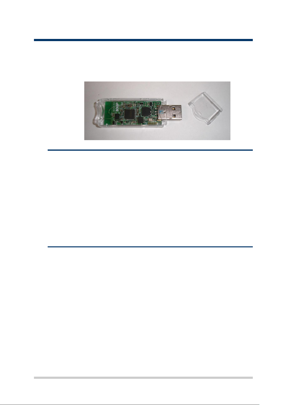
This manual provides a detailed reference for the JN5148 High-Power USB
Dongle, of type DR1131, supplied with JenNet-IP EK040 evaluation kit. The
dongle provides a platform for hardware development environment for wireless
microcontroller applications with a USB interface.
1.1 Features
The dongle has the following features:
JN5148-J01 device (mounted directly on the board)
Integrated PCB antenna
High-power capability
NXP LPC1343 USB interface and connector (interface chip is connected to
UART0 of the JN5148-J01 device)
Two LEDs (one red and one green)
This dongle is a high-power device with a radio transmission capability similar to
the high-power modules provided in the JenNet-IP EK040 evaluation kit.
1.2 Reference Design
A reference design (JN-RD-6034) for the JN5148 High-Power USB Dongle is
available from www.nxp.com/jennic/support. The reference design comprises a
ZIP file containing the following files:
This Reference Manual
The schematic diagram for the board
The BOM (Bill Of Materials) for the board
Gerbers for the board
4 © NXP Laboratories UK 2012 JN-RM-2064 v1.0
Page 5
JN5148 High-Power USB Dongle (DR1131)
Reference Manual
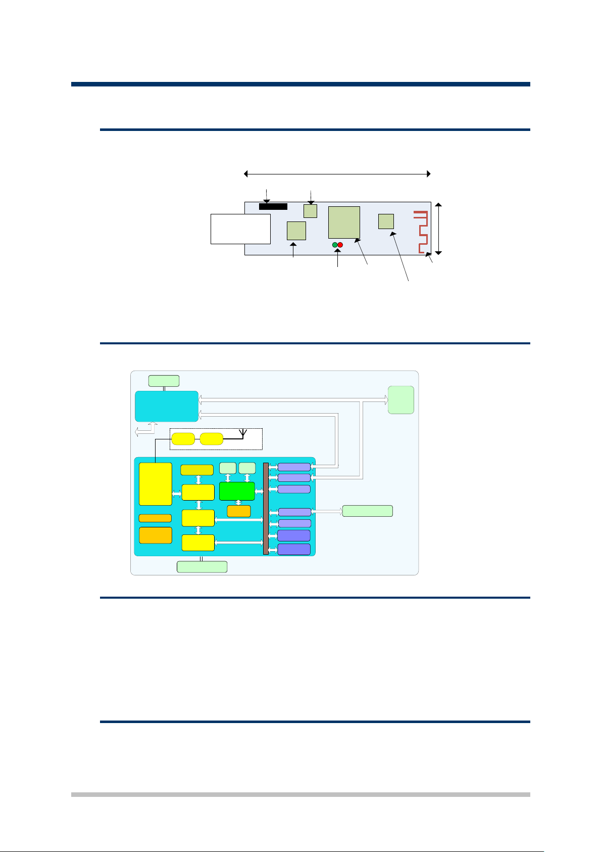
19mm
45mm
USB
JN5148
LEDS
HP Front End
LPC1343
Antenna
SPI Flash
LPC1343 Config
Connector
Timers
UART
12-bit ADC,
comparators
12-bit DACs,
temp sensor
SPI
RAM
128kB
128-bit AES
Encryption
Accelerator
2.4GHz
Radio
ROM
128kB
RISC CPU
Power
Management
XTAL
32.768 kHz
O-QPSK
Modem
IEEE802.15.4
MAC
Accelerator
512kB
Serial Flash
Memory
JN5148 chip
Integrated Antenna
32kHz ext Xtal
Sleep Counters
32-byte
OTP eFuse
Watchdog timer
Time of Flight
Engine
USB
LPC1343
Micro
XTAL
32 MHz
XTAL
12 MHz
SE2431L
Matching
2 Hardware Overview
2.1 Dongle Layout
Figure 1: DR1131 Board Layout
2.2 Dongle Block Diagram
2.3 LPC1343 Device
The LPC1343 device is connected to the USB connector and acts as an
JN-RM-2064 v1.0 © NXP Laboratories UK 2012 5
interface between the PC and the JN5148 device. The LPC1343 will enumerate
on the PC as two devices:
1. A mass storage device used to program the Flash device for the JN5148
2. A virtual COM port connected directly to UART0 on the JN5148
2.4 JN5148 Device
The JN5148 circuit is based around the standard JN5148 reference design.
Page 6

JN5148 High-Power USB Dongle (DR1131)
Reference Manual
2.5 High-Power Front-End
The front-end is a Skyworks SE2431L. This means that the dongle can achieve
22dBm output power and Rx sensitivity of -100dBm. The output of the front-end
is connected to a printed antenna.
2.6 LNA Bypass
If the dongle is used in the presence of very strong signals, such as Wi-Fi, then
there will be a performance improvement by switching off the Low-Noise
Amplifier (LNA) in the front-end to stop the input stage of the JN5148 device from
being overloaded with other signals. The LNA can be bypassed using DIO1 driving DIO1 low will bypass the LNA.
2.7 LEDs
The two LEDs are connected back-to-back between DIOs 16 and 17.
6 © NXP Laboratories UK 2012 JN-RM-2064 v1.0
Page 7
JN5148 High-Power USB Dongle (DR1131)
Reference Manual
3 Programming the LPC1343 Device
The LPC1343 device is supplied pre-programmed on all USB dongles. You
should never need to reprogram the firmware in the LPC1343 device when
developing applications for the JN5148 device.
If you are producing new USB dongles or are developing new ways to
communicate with the JN5148 device (i.e. new HID classes) then the mechanism
for reprogramming the LPC1343 is as follows.
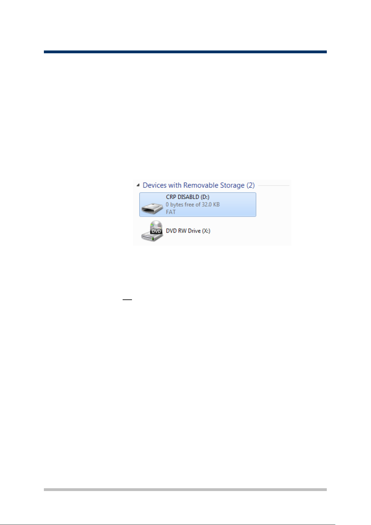
1. Insert the USB dongle into the PC with pins 2 and 6 of J4 connected
together.
2. Wait up to 30 seconds. The dongle will now appear in Windows Explorer
as a mass storage device with the title ‘CRP DISABLD’:
3. Rename your new binary FIRMWARE.BIN.
4. ‘Drag and drop’ or ‘copy and paste’ the new binary file onto the USB
dongle.
5. Remove the USB dongle from the PC and re-insert it, this time with J4 pins
2 and 6 not connected together.
Two pre-compiled binaries are available in the JN-RD-6034 reference design.
These are:
LPC1343_Firmware_0x10.bin: This binary should be used for devices
that store their MAC address at address 0x10, such as the JN5148-J01
and JN5142-J01.
LPC1343_Firmware_0x30.bin: This binary should be used for devices
that store their MAC address at address 0x30, such as the JN5148-001.
JN-RM-2064 v1.0 © NXP Laboratories UK 2012 7
Page 8

JN5148 High-Power USB Dongle (DR1131)
Reference Manual
4 Programming the JN5148 Device
4.1 Re-programming USB Dongles
You can easily re-programme a dongle with another binary file through a USB
port of your PC and the LPC1343 device on the dongle. The replacement binary
file must be a specially prepared file called FIRMWARE.BIN. When this file is
copied onto the mass storage device, the LPC1343 device holds the JN5148
device in reset and then programs the SPI Flash device directly, releasing the
reset once programming is complete. The LPC1343 device will also check the
MAC address in the SPI Flash device and preserve it though re-programming
operations if a new MAC address has not been specified in the new
FIRMWARE.BIN file.
4.2 Preparing the Binary File
Before a custom application binary file can be programmed into the USB dongle,
a utility called jn514x_firmware.exe must be run on the file to strip out a 4-byte
header. This utility is provided in the JenNet-IP SDK (JN-SW-4051) and is
located as follows:
C:/Jennic/Tools/NXP_USBDongle/jn514x_firmware.exe
The utility can be run from a bash shell using the following command:
/cygdrive/c/Jennic/Tools/NXP_USBDongle/jn514x_firmware.exe
with the following options:
-f is used to specify the name of the input file
-m is used to specify the IEEE/MAC address of the target device (: separated)
-c is used to specify the target chip type (in this case, should be JN5148J01)
Therefore, the required usage is:
.../jn514x_firmware.exe -f <app path/name> -m <MacAddress>
-c JN5148J01
4.3 Programming the Dongle
This re-programming of the dongle uses a simple ‘drag and drop’ method within
Windows Explorer, as follows:
1. Plug the USB dongle into a free USB port of your PC (if an ‘Installing driver’
message is displayed, refer to Section 4.4 below).
2. Open Windows Explorer - the dongle should appear as ‘Jennic_USB’.
3. If the dongle currently contains any files, delete them.
4. Within Windows Explorer, navigate to the new FIRMWARE.BIN file on your
PC, then ‘drag and drop’ or ‘copy and paste’ the new binary file onto the
USB dongle.
8 © NXP Laboratories UK 2012 JN-RM-2064 v1.0
Page 9

JN5148 High-Power USB Dongle (DR1131)
Reference Manual
4.4 Installing Device Driver for USB Dongle
1. The first time you plug the dongle into a USB port of your PC, an ‘Installing
driver’ message appears in the bottom-right corner of the screen. The
system will install most of the software required, but will leave the following
box:
2. Close the box and go to Start > Control Panel > System > Device
Manager. In the Device Manager, you will notice that the VCOM port is
accompanied by an exclamation mark:
3. Right-click on the VCOM port and from the context menu select 'Update
driver software..' and then select the manual installation method (bottom
option).
4. Use the Update Driver Software browser to navigate down to the folder
C:\Jennic\Tools\NXP_USBDongle\Drivers and then click Next.
The system will now install the software driver.
JN-RM-2064 v1.0 © NXP Laboratories UK 2012 9
Page 10

JN5148 High-Power USB Dongle (DR1131)
Reference Manual
5. You can check that the device driver has installed correctly as if it has, the
device NXP LPC1343 will appear in the Ports (COM & LPT) section and
will appear as a USB mass storage device in the USB Controllers section.
Your dongle is now ready to use.
10 © NXP Laboratories UK 2012 JN-RM-2064 v1.0
Page 11

JN5148 High-Power USB Dongle (DR1131)
Reference Manual
5 Compliance Statements & Documentation
5.1 FCC Statements and Documentation
This section contains the Federal Communication Commission (FCC) statements
and documents.
5.1.1 High-Power Module Usage Limitation
The high-power module variants are classified as 'mobile' devices pursuant with
FCC §2.1091 and must not be used at a distance of less than 20 cm (8") from
any person.
5.1.2 Federal Communication Commission Interference
Statement
This equipment has been tested and found to comply with the limits for a Class B
digital device, pursuant to Part 15 of the FCC Rules. These limits are designed to
provide reasonable protection against harmful interference in a residential
installation. This equipment generates, uses, and can radiate radio frequency
energy and, if not installed and used in accordance with the instructions, may
cause harmful interference to radio communications. However, there is no
guarantee that interference will not occur in a particular installation. If this
equipment does cause harmful interference to radio or television reception,
which can be determined by turning the equipment off and on, the user is
encouraged to try to correct the interference by one of the following measures:
- Reorient or relocate the receiving antenna.
- Increase the separation between the equipment and receiver.
- Connect the equipment into an outlet on a circuit different from that to which the
receiver is connected.
- Consult the dealer or an experienced radio/TV technician for help.
This device complies with Part 15 of the FCC Rules. Operation is subject to the
following two conditions: (1) This device may not cause harmful interference, and
(2) this device must accept any interference received, including interference that
may cause undesired operation.
FCC Caution: Any changes or modifications not expressly approved by the party
responsible for compliance could void the user's authority to operate this
equipment.
JN-RM-2064 v1.0 © NXP Laboratories UK 2012 11
Page 12

JN5148 High-Power USB Dongle (DR1131)
Reference Manual
5.1.3 WARNING!
FCC Radiation Exposure Statement:
This portable equipment with its integrated antenna complies with FCC’s RF
radiation exposure limits set forth for an uncontrolled environment. To maintain
compliance follow the instructions below;
Avoid direct contact to the antenna, or keep it to a minimum while using this
equipment.
Please observe the usage limitation notice in this user guide.
5.1.4 USB Dongle usage recommendation
It is strongly recommended for best performance and minimum RF exposure that
the Dongle is used with the supplied USB extension cable.
12 © NXP Laboratories UK 2012 JN-RM-2064 v1.0
Page 13

JN5148 High-Power USB Dongle (DR1131)
Reference Manual
Version
Date
Description
1.0
25-July-2012
First release
Revision History
JN-RM-2064 v1.0 © NXP Laboratories UK 2012 13
Page 14

JN5148 High-Power USB Dongle (DR1131)
Reference Manual
NXP Laboratories UK Ltd
(Formerly Jennic Ltd)
Furnival Street
Sheffield
S1 4QT
United Kingdom
Tel: +44 (0)114 281 2655
Fax: +44 (0)114 281 2951
For the contact details of your local NXP/Jennic office or distributor, refer to:
www.nxp.com/jennic
Important Notice
Limited warranty and liability — Information in this document is believed to be accurate and reliable.
However, NXP Semiconductors does not give any representations or warranties, expressed or implied, as to
the accuracy or completeness of such information and shall have no liability for the consequences of use of
such information. NXP Semiconductors takes no responsibility for the content in this document if provided by
an information source outside of NXP Semiconductors.
In no event shall NXP Semiconductors be liable for any indirect, incidental, punitive, special or consequential
damages (including - without limitation - lost profits, lost savings, business interruption, costs related to the
removal or replacement of any products or rework charges) whether or not such damages are based on tort
(including negligence), warranty, breach of contract or any other legal theory.
Notwithstanding any damages that customer might incur for any reason whatsoever, NXP Semiconductors’
aggregate and cumulative liability towards customer for the products described herein shall be limited in
accordance with the Terms and conditions of commercial sale of NXP Semiconductors.
Right to make changes — NXP Semiconductors reserves the right to make changes to information published
in this document, including without limitation specifications and product descriptions, at any time and without
notice. This document supersedes and replaces all information supplied prior to the publication hereof.
Suitability for use — NXP Semiconductors products are not designed, authorized or warranted to be suitable
for use in life support, life-critical or safety-critical systems or equipment, nor in applications where failure or
malfunction of an NXP Semiconductors product can reasonably be expected to result in personal injury, death
or severe property or environmental damage. NXP Semiconductors and its suppliers accept no liability for
inclusion and/or use of NXP Semiconductors products in such equipment or applications and therefore such
inclusion and/or use is at the customer’s own risk.
Applications — Applications that are described herein for any of these products are for illustrative purposes
only. NXP Semiconductors makes no representation or warranty that such applications will be suitable for the
specified use without further testing or modification.
Customers are responsible for the design and operation of their applications and products using NXP
Semiconductors products, and NXP Semiconductors accepts no liability for any assistance with applications or
customer product design. It is customer’s sole responsibility to determine whether the NXP Semiconductors
product is suitable and fit for the customer’s applications and products planned, as well as for the planned
application and use of customer’s third party customer(s). Customers should provide appropriate design and
operating safeguards to minimize the risks associated with their applications and products.
NXP Semiconductors does not accept any liability related to any default, damage, costs or problem which is
based on any weakness or default in the customer’s applications or products, or the application or use by
customer’s third party customer(s). Customer is responsible for doing all necessary testing for the customer’s
applications and products using NXP Semiconductors products in order to avoid a default of the applications
and the products or of the application or use by customer’s third party customer(s). NXP does not accept any
liability in this respect.
Export control — This document as well as the item(s) described herein may be subject to export control
regulations. Export might require a prior authorization from competent authorities.
14 © NXP Laboratories UK 2012 JN-RM-2064 v1.0
 Loading...