

Page 1
Data Sheet: JN5148-001-Myy
JenNet, ZigBee PRO and IEEE802.15.4 Module
Timers
UARTs
12-bit ADC,
comparators
12-bit DACs,
temp sensor
2-wire serial
SPI
RAM
128kB
128-bit AES
Encryption
Accelerator
2.4GHz
Radio
ROM
128kB
RISC CPU
Power
Management
XTAL
O-QPSK
Modem
IEEE802.15.4
MAC
Accelerator
512kB Serial
Flash Memory
JN5148 chip
Power
Matching
uFl
Connector
Matching
Integrated Antenna
Matching
uFl
Connector
PA / LNA
External
Antenna
M00 Option
M03 Option
M06 Option
4-Wire Audio
Sleep Counters
32-byte
OTP eFuse
Watchdog timer
Time of Flight
Engine
Overview
The JN5148-001-Myy fam ily is a range of ultr a low power, high perf ormance surface
mount modules targeted at JenNet and ZigBee PRO networking applications,
enabling users to realise products with minimum time to market and at the lowest
cost. They rem ove the need for expensive and lengthy developm ent of custom RF
board designs and test suites. The modules use NXP’s JN5148 wireless
microcontroller to provide a comprehensive solution with large memory, high CPU
and radio performance and all RF components included. All that is required to
develop and manufac ture wireless control or s ensing products is to connect a po wer
supply and peripherals such as switches, actuators and sensors, considerably
simplifying product develop ment.
Three module variants are available: JN5148-001-M00 with an integrated antenna,
JN5148-001-M03 with an antenna connector and the JN5148-001-M06 with an
antenna connector, power amplifier and LNA for extended range. The m odules can
implement network ing stacks such as J enNet and ZigBee PRO, as well as custom er
applications
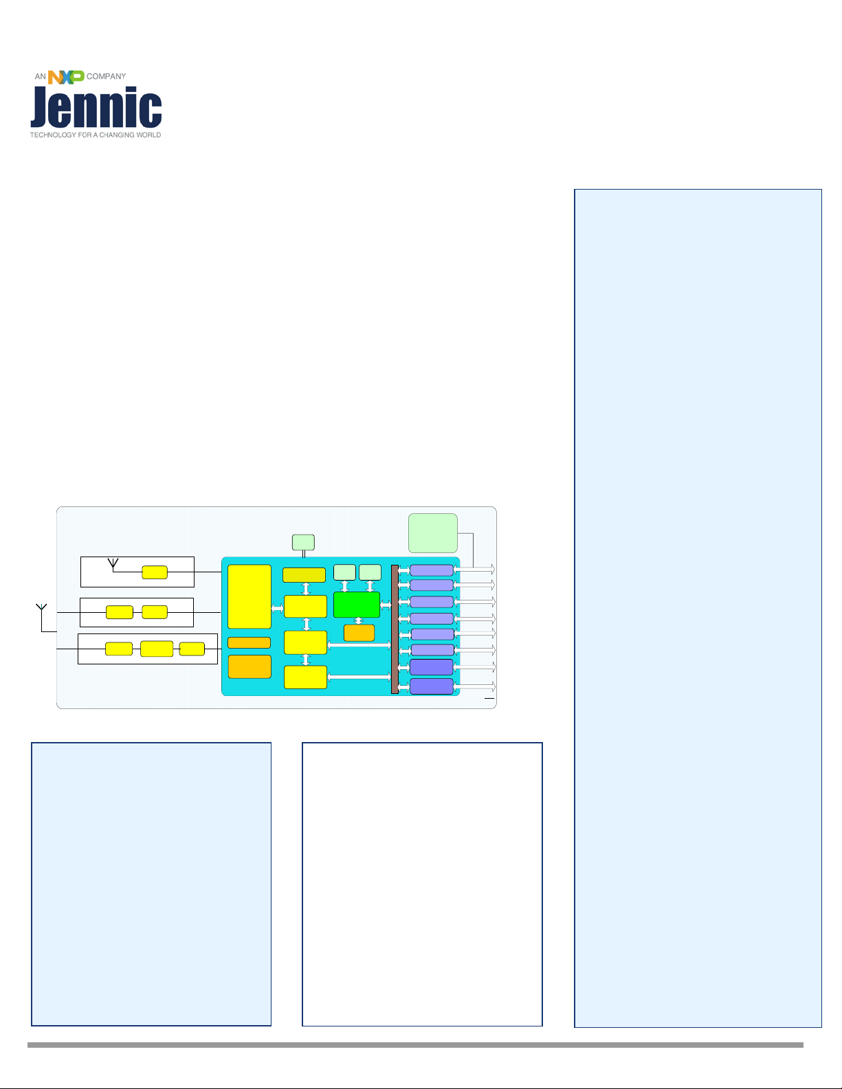
Module Block Diagram
Benefits
• Microminiature module solutions
• Ready to use in products
• Minimises product development
time
• No RF test required for systems
• Compliant with FCC part 15
rules, IC Canada RSS 210e,
ETSI EN 300-328
JN-DS-JN5148-001-Myy 1v5 © NXP Laboratories UK 2012
Applications
• Robust and secure low power
wireless applications
• ZigBee PRO and JenNet
networks
• Home and commercial building
automation
• Utilities metering (e.g. AMR)
• Location Aware services (e.g.
Asset Tracking)
• Toys and gaming peripherals
• Industrial systems
• Telemetry
• Remote Control
Features: Module
• 2.4GHz IEEE802.15.4, JenNet and
ZigBee PRO compatible
JN5148-001-M00/03
•
up to 1km range (Ext antenna)
M00: integral antenna 18x32mm
M03: uFl connector 18x30mm
o TX power +2.5dBm
o Receiver sensitivity –95dBm
o TX current 15mA
o RX current 17.5mA
o 2.3-3.6V operation
• JN5148-001-M06
up to 4km range (Ext Antenna)
o 22dBm TX Power
o 18dBm TX power (M04
compatible)
o Receiver sensitivity -100dBm
o uFl connector
o TX current 84mA
o RX current 23mA
o 18x41mm
o 2.3-3.6V operation
Features: Microcontroller
• 32-bit RISC CPU, up to 32MIPs with
low power
• 128kB ROM stores system code
• 128kB RAM stores system data and
bootloaded program code
• 4Mbit serial flash for program code
and data
• On chip OTP efuse
• JTAG debug interface
• 4-input 12-bit ADC, 2 12-bit DACs, 2
comparators
• 3 application timer/counters,
• 2 UARTs
• SPI port with 5 selects
• 2-wire serial interface
• 4-wire digital audio interface
• Watchdog timer
• Up to 21 DIO
Industrial temp (-40°C to +85°C)
Lead-free and RoHS compliant
Page 2

Contents
1. Introduction 3
1.1. Variants 3
1.2. Regulatory Approvals 3
2. Specifications 4
3. Product Development 6
3.1. JN5148 Single Chip Wireless Microcontroller 6
4. Pin Configurations 7
4.1. Pin Assignment 8
4.2. Pin Descriptions 9
4.2.1 Power Supplies 9
4.2.2 SPI Memory Connections 9
5. Electrical Characteristics 10
5.1. Maximum Ratings 10
5.2. Operating Conditions 10
Appendix A Additional Information 11
A.1 Outline Drawing 11
A.2 Module PCB Footprint 14
A.3 Manufacturing 15
A.3.1 Reflow Profile 15
A.3.2 Soldering Paste and Cleaning 15
A.4 Ordering Information 16
A.5 Tape and Reel Information: 17
A.5.1 Tape Orientation and dimensions 17
A.5.2 Cover tape details 17
A.5.3 Leader and Trailer 18
A.5.4 Reel Dimensions: 18
A.6 Related Documents 18
A.7 Federal Communication Commission Interference Statement 19
A.7.1 Antennas approved by FCC for use with JN5148 modules 20
A.7.2 High Power Module usage limitation 20
A.7.3 FCC End Product Labelling 20
A.8 Industry Canada Statement 21
A.8.1 Industry Canada End Product Labelling 21
A.9 European R & TTE Directive 1999/5/EC Statement 21
A.10 RoHS Compliance 22
A.11 Status Information 22
A.12 Disclaimers 22
Version Control 23
ii JN-DS-JN5148-001-Myy 1v5 © NXP Laboratories UK 2012
Page 3

1. Introduction
The JN5148-001-Myy module family provides designers with a ready made component that provides a fully
integrated solution for applications, using the IEEE802.15.4 standard in the 2.4-2.5GHz ISM frequency band [1],
including JenNet and ZigBee PRO, and can be quickly and easily included in product designs. The modules
integrate all of the RF components required, removing the need to perform expensive RF design and test. Products
can be designed by simply connecting sensors and switches to the module IO pins. The modules use NXP’s single
chip IEEE802.15.4 Wireless Microcontroller, allowing designers to make use of the extensive chip development
support material. Hence, this range of modules allows designers to bring wireless applications to market in the
minimum time with significantly reduced development effort and cost.
Three variants are available: JN5148-001-M00 (standard module with integral antenna), JN5148-001-M03 (standard
module with uFl connector for use with external antennae) and JN5148-001-M06 (high RF power with uFL connector,
improved sensitivity module for evaluation of extended range applications). All modules have FCC modular
approvals, CE approval and are compliant with EU regulations. The variants available are described below.
1.1. Variants
Variant Description FCCID Industry Canada ID
JN5148-001-M00 Standard Power, integrated antenna TYOJN5148M0 IC: 7438A-CYO5148M0
JN5148-001-M03 Standard Power, uFl connector TYOJN5148M3 IC: 7438A-CYO5148M3
JN5148-001-M06 High Power, uFl connector TYOJN5148M6 IC: 7438A-CYO5148M6
1.2. Regulator y Approvals
All module types have been tested against the requirements of the following European standards. For the Radio, EN
300 328 v1.7.1. EMC, EN 301 489-17 v2.1.1 and the Basic Safety Assessment (BSA) EN 60950-1:2006, a Notified
Body statement of opinion for this standard is available on request. The High Power module with M06 suffix is
approved for use in Europe with reduced output power: +10dBm EIRP is the maximum permitted in Europe.
Additionally, all module types have received FCC “Modular Approvals”, in compliance with CFR 47 FCC part 15
regulations and in accordance to FCC Public notice DA00-1407, appendix A.7 contains det ails on the conditi ons
applying to this modular approval. The modules are approved for use with a range of different antennas; further
details of which can be found in section Appendix A.6.1. The modular approvals notice and test reports are available
on request.
The high power module variant is classified as ‘mobile’ device pursuant with FCC § 2.1091 and must not be used at a
distance of less than 20 cm (8”) from any person.
In addition, all modules have Industry Canada modular approval and RSS210e Issue 7 (June 2007) certification.
© NXP Laboratories UK 2012 JN-DS-JN5148-001-Myy 1v5 3
Page 4

Typical DC Characteristics
Notes
JN5148-001-
M00/03
JN5148-001-
M06
Deep sleep current
1.3uA
120nA
Sleep current
2.6uA
1.25uA
With active sleep timer
Radio transmit current (M04 Compatibility Mode)
15mA
84mA
CPU in doze, radio transmitting
Radio transmit current
-
178mA
CPU in doze, radio transmitting
Radio transmit current (ETSI Mode)
-
48mA
CPU in doze, radio transmitting
Radio receive current
17.5mA
23mA
CPU in doze, radio receiving
temperature and ageing
Typical RF Characteristics
Notes
Nominal for 1% PER, as per
802.15.4 section 6.5.3.3 (Note 1)
Transmit power (M04 Compatibility Mode)
+2.5dBm
+18dBm
Nominal (Note 2)
Transmit power
-
+22dBm
Nominal
Transmit power (ETSI Mode)
-
+8dBm/MHz
Nominal (Note 3)
sensitivity
dBm
dBm
RF Port impedance – uFl conn ector
50 ohm
50 ohm
2.4 - 2.5GHz
Rx Spurious Emissions
-61dBm
-69dBm
Measured conducted into 50ohms
Tx Spurious Emissions
-40dBm
-49dBm
Measured conducted into 50ohms
VSWR (max)
2:1
2:1
2.4 - 2.5GHz
Peripherals
Notes
Master SPI port
5 selects
3 selects
250kHz - 16MHz
Two UARTs
16550 compatible
Two-wire serial I/F (compatible with SMbus & I2C)
Up to 400kHz
capture/compare facility, Tick timer
Two programmable Sleep Timers
32kHz clock
Digital IO lines (multiplexed with UARTs, timers
and SPI selects)
21
19
Two channel Digital-to-Analogue converter
12-bit, up to 100ks/s
2. Specifications
Most specification parameters for the modules are specified in the chip datasheet - JN-DS-JN5148 Wireless
Microcontroller Datasheet, [2]. Where there are differences, the par amet ers are defi ned her e.
VDD=3.0V @ +25°C
Centre frequency accuracy +/-25ppm +/-25ppm
Receive sensitivity -95dBm -100dBm
Maximum input signal +5dBm -5dBm
RSSI range
Slave SPI port
-95 to -10
-105 to -20
Additional +/-15ppm allowance for
For 1% PER, measured as
250kHz - 8MHz
Three programmable Timer/Counters with
Four channel Analogue-to-Digital converter
4 JN-DS-JN5148-001-Myy 1v5 © NXP Laboratories UK 2012
16MHz clock
12-bit, up to 100ks/s
Page 5

Two programmable analogue comparators
Ultra low power mode for sleep
Internal temperature sensor and battery monitor
The performance of all peripherals is defined in the JN-DS-JN5148 Wireless Microcontroller Datasheet [2]
Note 1: Sensitivity is defined for conducted measurements on connectorised modules. Modules with an integrated
antenna have approximately 4 dB less e.i.r.p and reciprocal receive sensitivity.
Note 2: It is possible to operate the M06 module with similar output power to the JN5148-001-M04 modules by
implementing a small change in the software as provided in the latest SDK.
Note 3: ETSI mode is achieved through a software setting as provided in the latest SDK. Note that this is different to
the equivalent setting for the JN5148-001-M04.
© NXP Laboratories UK 2012 JN-DS-JN5148-001-Myy 1v5 5
Page 6

3. Product Development
NXP supplies all the development tools and networking stacks needed to enable end-product development to occur
quickly and efficiently. These are all freely available from www.nxp.com/jennic. A range of evaluation/developer kits
is also available, allowing products to be quickly bread boarded. Efficient development of software applications is
enabled by the provision of a complete, unlimited, software developer kit. Together with the available libraries for the
IEEE802.15.4 MAC and the JenNet and ZigBee PRO network stacks, this package provides everything required to
develop application code and to trial it with hardware representative of the final module.
The modules can be user programmed both in development and in production using software supplied by NXP.
Access to the on-chip peripherals, MAC and network stack software is provided through specific APIs. This
information is available on the NXP support website, together with many example applications, user guides, reference
manuals and application notes.
3.1. JN5148 Single Chip Wireless Microcontroller
The JN5148-001-Myy series is constructed around the JN5148-001 single chip wireless microcontroller, which
includes the radio system, a 32-bit RISC CPU, ROM and RAM memory and a range of analogue and digital
peripherals.
The chip is described fully in JN-DS-JN5148 Wireless Microcontroller Datasheet [2].
The module also includes a 4Mbit serial flash memory, which holds the application code that is loaded into the
JN5148 during the boot sequence and provides stati c data st or age, requ ir ed by the applic at ion.
6 JN-DS-JN5148-001-Myy 1v5 © NXP Laboratories UK 2012
 Loading...